JP6727897B2 - Solid-state imaging device, method of manufacturing solid-state imaging device, and imaging system - Google Patents
Solid-state imaging device, method of manufacturing solid-state imaging device, and imaging system Download PDFInfo
- Publication number
- JP6727897B2 JP6727897B2 JP2016081833A JP2016081833A JP6727897B2 JP 6727897 B2 JP6727897 B2 JP 6727897B2 JP 2016081833 A JP2016081833 A JP 2016081833A JP 2016081833 A JP2016081833 A JP 2016081833A JP 6727897 B2 JP6727897 B2 JP 6727897B2
- Authority
- JP
- Japan
- Prior art keywords
- region
- gate electrode
- film
- imaging device
- solid
- Prior art date
- Legal status (The legal status is an assumption and is not a legal conclusion. Google has not performed a legal analysis and makes no representation as to the accuracy of the status listed.)
- Active
Links
Images


Description
本発明は、固体撮像装置、固体撮像装置の製造方法、および撮像システムに関する。 The present invention relates to a solid-state imaging device, a method for manufacturing a solid-state imaging device, and an imaging system.
CMOSイメージセンサ、CCDイメージセンサなどの固体撮像装置において、光電変換を行う光電変換部以外の部分に光が入射されるのを防ぐ遮光部材が設けられている。例えば、グローバル電子シャッタ(全画素一括同時露光)機能を備えたCMOSイメージセンサは、光電変換部から転送された電荷を保持する電荷保持部を有している。電荷保持部に光が入射して光電変換が起こると、光電変換された電荷がノイズとなり、画質が劣化する虞がある。このため、電荷保持部を遮光部材で覆い、光の入射を防いでいる。また、CCDイメージセンサにおいてもCMOSイメージセンサと同様に、読み出し部に光が入射するとノイズの原因となるため、読み出し部を遮光部材で覆っている。 A solid-state imaging device such as a CMOS image sensor or a CCD image sensor is provided with a light blocking member that prevents light from entering a portion other than a photoelectric conversion unit that performs photoelectric conversion. For example, a CMOS image sensor having a global electronic shutter (batch simultaneous exposure for all pixels) function has a charge holding unit that holds the charges transferred from the photoelectric conversion unit. When light enters the charge holding portion and photoelectric conversion occurs, the photoelectrically converted charges become noise, which may deteriorate image quality. Therefore, the charge holding portion is covered with a light shielding member to prevent light from entering. Further, in the CCD image sensor as well as in the CMOS image sensor, when light enters the reading section, it causes noise, so the reading section is covered with a light shielding member.
遮光部材を有する固体撮像装置においては、基板と遮光部材との間に光学的に透明な層間絶縁膜が存在するため、この層間絶縁膜を介して侵入する光を防ぐことによって遮光性能の向上が図られている。特許文献1では、遮光部材の下に配される絶縁膜をエッチングすることでこの絶縁膜の膜厚を薄くしている。遮光部材の下の絶縁膜を薄くして光電変換部と遮光部材の下面との距離を縮めることで、電荷保持部への光の漏れを抑制し、遮光性能の向上を図っている。
In a solid-state imaging device having a light blocking member, since an optically transparent interlayer insulating film exists between the substrate and the light blocking member, the light blocking performance can be improved by preventing light entering through the interlayer insulating film. Has been planned. In
ゲート電極間の間隔がある程度の大きさを有する場合には、隣り合うゲート電極上に絶縁膜を形成し、遮光膜を製膜した場合、ゲート電極間で絶縁膜が十分平らになる部分があるため、遮光膜をエッチングしても残渣は発生しにくい。一方、半導体プロセスの微細化により、ゲート電極間の間隔が狭くなる。この狭い間隔上に遮光部材となる遮光膜を成膜し、遮光膜をエッチングすると、狭い間隔の内部に遮光膜の残渣が存在する場合がある。このような残渣はリークの原因となり得る。特許文献1においては、遮光膜の下に絶縁膜を成膜することにより、ゲート電極間、配線間の凹部を埋め込み、段差を緩和している。これにより、遮光膜のエッチング残渣の発生を低減することができる。しかしながら、特許文献1においては、ある一定の間隔よりも狭い凹部を埋め込むことはできるものの、当該間隔以上の凹部を平坦に埋め込みきれず、細い隙間が残り、この隙間の中に遮光部材が残ることがあった。たとえ埋め込む絶縁膜を厚くしたとしも、凹部の間隔によっては隙間が生じてしまい、残渣の発生を完全に防止することはできなかった。
When the gap between the gate electrodes has a certain size, when the insulating film is formed on the adjacent gate electrodes and the light-shielding film is formed, there is a portion where the insulating film is sufficiently flat between the gate electrodes. Therefore, even if the light-shielding film is etched, residues are unlikely to occur. On the other hand, due to the miniaturization of the semiconductor process, the distance between the gate electrodes becomes narrow. When a light-shielding film serving as a light-shielding member is formed on this narrow space and the light-shielding film is etched, residues of the light-shielding film may exist inside the narrow space. Such residues can cause leaks. In
また、ゲート電極の段差に起因して、絶縁膜表面の平坦性が損ねられると、遮光部材およびその上に形成する構造体の平坦性も同様に悪化し、ひいては歩留まりも低下し得る。本発明の目的は、遮光部材による遮光性能を維持するとともに、歩留まりを向上しうる固体撮像装置、固体撮像装置の製造方法、および撮像システムを提供することにある。 Further, if the flatness of the surface of the insulating film is impaired due to the step of the gate electrode, the flatness of the light shielding member and the structure formed thereon may be similarly deteriorated, and the yield may be reduced. An object of the present invention is to provide a solid-state imaging device, a method for manufacturing the solid-state imaging device, and an imaging system that can improve the yield while maintaining the light-shielding performance of the light-shielding member.
本発明の一実施形態に係る固体撮像装置の製造法は、第1の領域、第2の領域、第3の領域及び第4の領域を有する基板の上に、第1のトランジスタの第1のゲート電極と、前記第1のゲート電極に隣接する、第2のトランジスタの第2のゲート電極とを、前記第1のゲート電極が前記第1の領域の上に位置し、前記第2のゲート電極が前記第2の領域の上に位置し、前記第1のゲート電極と前記第2のゲート電極との間隙が前記第4の領域の上に位置するように形成する工程と、前記第4の領域、前記第1のゲート電極及び前記第2のゲート電極を覆う絶縁体膜を成膜する工程と、前記絶縁体膜の上に、前記第3の領域及び前記第4の領域を覆う遮光性の材料よりなる膜を成膜する工程と、前記絶縁体膜を挟んでボイドの上に位置している前記遮光性の材料よりなる膜のうち、少なくとも前記第4の領域の上に位置する一部をエッチングで除去し、前記遮光性の材料よりなる膜から前記第3の領域の上に遮光部材を形成する工程と、前記遮光部材、前記第1のゲート電極及び前記第2のゲート電極を覆う絶縁膜を形成する工程と、前記絶縁膜を貫通して前記第1のトランジスタ及び前記第2のトランジスタのいずれかに接続するコンタクトプラグを形成する工程と、
前記絶縁膜の上に、前記コンタクトプラグに接続する配線を形成する工程と、を有し、前記遮光性の材料よりなる膜を成膜する工程において、前記絶縁体膜と前記第4の領域との間にボイドが存在する。
A method for manufacturing a solid-state imaging device according to an embodiment of the present invention includes a first transistor, a first region, a second region, a third region, and a fourth region on a substrate having a first region, a second region, a third region, and a fourth region . a gate electrode adjacent to said first gate electrode and a second gate electrode of the second transistor, the first gate electrode is positioned on the first region, said second gate a step of the electrode is positioned on the second region, the gap between the first gate electrode and the second gate electrode can be on the top of the fourth region, said fourth Forming an insulator film covering the first region and the first gate electrode and the second gate electrode, and shading covering the third region and the fourth region on the insulator film. a step of forming a film made of sexual material, of the light-shielding made of a material film which is located above the void across the insulator film, located on at least the fourth region Forming a light-shielding member on the third region from a film made of the light-shielding material by etching a part of the material; the light- shielding member, the first gate electrode, and the second gate electrode Forming an insulating film covering the insulating film, and forming a contact plug penetrating the insulating film to connect to either the first transistor or the second transistor,
On the insulating film, have a, and forming a wiring connected to the contact plug, in the step of forming a film made of the light shielding material, and the insulator film and the fourth region There is a void between them.
本発明の他の実施形態に係る固体撮像装置の製造方法は、前記遮光性の材料よりなる膜のエッチング時間に対する前記絶縁体膜のエッチング時間の比をa、前記遮光部材となる前記遮光性の材料よりなる膜と前記絶縁体膜のエッチング選択比をb、前記絶縁体膜の膜厚をt、前記遮光部材の膜厚をd1としたとき、前記絶縁体膜が、a×b×d 1 ≦tを満たすように形成される。
Manufacturing method of another embodiment solid-state imaging device according to the embodiment of the present invention, the etching time of the ratio of the insulator layer to the etch time of the light-shielding made of a material film a, the light-shielding of the light shielding member When the etching selection ratio between the film made of a material and the insulating film is b, the film thickness of the insulating film is t, and the film thickness of the light shielding member is d 1 , the insulating film is a×b×d It is formed so as to satisfy 1 ≦t .
また、本発明の他の実施形態に係る固体撮像装置は、第1の領域、第2の領域、第3の領域及び第4の領域を有する基板と、前記第1の領域の上に位置する、第1のトランジスタの第1のゲート電極と、前記第2の領域の上に位置し、前記第1のゲート電極に隣り合う、第2のトランジスタの第2のゲート電極と、前記第3の領域、前記第4の領域、前記第1のゲート電極及び前記第2のゲート電極を覆う絶縁膜と、前記絶縁膜と前記基板の間に配され、前記第3の領域、前記第4の領域、前記第1のゲート電極及び前記第2のゲート電極を覆う絶縁体膜と、前記絶縁膜と前記第3の領域の間に設けられた遮光部材と、
前記絶縁膜の上に設けられた配線と、を備え、前記絶縁体膜のうちの前記第3の領域を覆う部分が前記遮光部材と前記第3の領域の間に位置し、前記第1のゲート電極と前記第2のゲート電極の間隙が前記第4の領域の上に位置し、前記絶縁体膜のうちの前記第4の領域を覆う部分と前記第4の領域の間にボイドが存在する。
A solid-state imaging device according to another embodiment of the present invention is located on the substrate having the first region, the second region, the third region, and the fourth region, and is located on the first region. A second gate electrode of a second transistor located above the first gate electrode of the first transistor and the second region and adjacent to the first gate electrode, and the third gate electrode of the second transistor. A region, the fourth region, an insulating film that covers the first gate electrode and the second gate electrode, and the insulating film is disposed between the insulating film and the substrate, and the third region and the fourth region. An insulator film covering the first gate electrode and the second gate electrode, and a light blocking member provided between the insulating film and the third region,
A wiring provided on the insulating film, wherein a portion of the insulating film covering the third region is located between the light shielding member and the third region , located in the gap of said gate electrode a second gate electrode over the fourth region, there is a void between said fourth region and said fourth region covering part of said insulator layer To do.
本発明によれば、固体撮像装置の遮光性能を維持したまま歩留まりを向上することができる。 According to the present invention, the yield can be improved while maintaining the light shielding performance of the solid-state imaging device.
(第1実施形態)
本発明の第1実施形態による固体撮像装置およびその製造方法について、図面を参照しながら説明する。図1は本実施形態に係る固体撮像装置のブロック図である。固体撮像装置は、行列状に配列された複数の画素回路1を有する画素領域10と、画素領域の周辺に位置し、周辺回路が配された周辺領域20を備える。画素回路1は光電変換を行う光電変換部、電荷を読み出すための読み出し部を備える。読み出し部は、電荷を転送する転送トランジスタ、電荷電圧変換部をリセットするトランジスタ、電荷電圧変換部の電位に応じた信号を出力する増幅トランジスタ、増幅トランジスタを選択するためのトランジスタを含む。また、読み出し部は光電変換部からの電荷を保持する電荷保持部を含み得る。光電変換部以外の回路部分、例えば電荷保持部は遮光部材によって入射光が遮られる。また、画素領域10には、分光感度特性を制御するためのカラーフィルタ、集光のためのマイクロレンズが光電変換部上に設けられており、各光電変換部間には混色を防ぐための遮光部材が形成され得る。さらに、画素領域10には、有効な画素以外に、光電変換部が遮光されたオプティカルブラック画素、光電変換部を有さないダミー画素などのように画像を出力しない画素が含まれ得る。
(First embodiment)
The solid-state imaging device and the method for manufacturing the same according to the first embodiment of the present invention will be described with reference to the drawings. FIG. 1 is a block diagram of a solid-state imaging device according to this embodiment. The solid-state imaging device includes a
周辺領域20は垂直走査回路21、列増幅回路22、水平走査回路23、出力部24を備える。垂直走査回路21は、画素回路1のトランジスタをオン(導通状態)またはオフ(非導通状態)に制御するための制御信号を供給する。垂直信号線11は、画素回路1の各列に設けられ、画素回路1からの信号を列ごとに読み出す。列増幅回路22は差動増幅回路およびサンプル・ホールド回路を備え、垂直信号線11に出力された画素信号を増幅する。水平走査回路23は、各列の増幅器に接続されたスイッチと、該スイッチをオンまたはオフに制御するための制御信号を供給する。出力部24はバッファアンプ、差動増幅器などから構成され、列増幅回路22からの画素信号を固体撮像装置の外部の信号処理部に出力する。出力された画素信号は信号処理部によって、アナログ/デジタル変換、入力データの補正などの処理が行われる。なお、固体撮像装置はアナログ/デジタル変換の機能を備えたいわゆるデジタルセンサであっても良い。
The
図2は、本実施形態による固体撮像装置の概略断面図である。ここでは、平面視において隣り合う任意の2つの第1のトランジスタ206、第2のトランジスタ207が示されている。トランジスタ206、207は、一例では、画素回路1を構成するトランジスタである。なお、隣り合う2つのトランジスタ206、207は互いに隣り合う一対のゲート電極201、202を有し、これらのゲート電極201、202の間にはボイド302が存在している。このように間にボイド302が存在する一対のゲート電極を有するトランジスタは、画素回路1、周辺回路のいずれのトランジスタであっても良い。
FIG. 2 is a schematic cross-sectional view of the solid-state imaging device according to the present embodiment. Here, two arbitrary
半導体基板100はX軸方向、Y軸方向を含むX−Y平面に平行な表面を有し、半導体基板100には、Z軸方向(第1の方向)に所定の厚さの第1導電型(例えばP型)のウェル101が設けられている。ウェル101が形成された半導体基板100の表面部には、活性領域を画定する素子分離領域102が設けられている。素子分離領域102により画定された活性領域には、ウェル101とは逆導電型(例えばN型)の不純物領域203、204、205が互いに離間して設けられている。
The
不純物領域203と不純物領域204との間の半導体領域(チャネル領域)上には、ゲート絶縁膜103を介してゲート電極201が設けられている。これにより、ソース/ドレイン領域を構成する不純物領域203、204とゲート電極201とを有するトランジスタ206が構成されている。ここで、ソース/ドレイン領域とは、トランジスタのソースおよびドレインの少なくともいずれかとして機能し得る半導体領域を意味する。トランジスタの駆動方法によっては、同一の半導体領域がソースとして機能する場合とドレインとして機能する場合がありうるし、同一の半導体領域が或るトランジスタのソースとして機能し、別のトランジスタのドレインとして機能する場合もある。同様に、不純物領域204と不純物領域205との間の半導体領域(チャネル領域)上には、ゲート絶縁膜103を介してゲート電極202が設けられている。これにより、ソース/ドレイン領域を構成する不純物領域204、205とゲート電極202とを有するトランジスタ207が構成されている。これら2つのトランジスタ206、207は、一方のソース/ドレイン領域(不純物領域204)を共有している。2つのトランジスタ206、207のゲート電極201、202の間隔は例えば1.0μm以下程度に狭くなっている。典型的にはゲート電極201とゲート電極202の間隔は、ゲート電極201とゲート電極202の厚さの和より小さく、0.5μm以下である。ゲート電極201とゲート電極202の間隔は、0.1μm以上でありうる。
A
なお、ここでいう部材の厚さ、膜厚とは、半導体基板100の平面視に垂直なZ軸方向(第1の方向)における長さを指す。半導体基板100上に後述するゲート電極、絶縁対膜、遮光部材などの層が積層される方向をZ軸方向と定義し得る。以下の説明において、特に断り書きのない限り、部材の厚さ、膜厚はZ軸方向の長さを指すものとする。
In addition, the thickness and the film thickness of the member here refer to the length in the Z-axis direction (first direction) perpendicular to the plan view of the
トランジスタ206、207が設けられた半導体基板100上には、絶縁体膜301が設けられている。絶縁体膜301は、ゲート電極201とゲート電極202との間隙に完全には埋め込まれておらず、ゲート電極201とゲート電極202との間の領域の少なくとも一部はボイド(空孔)302が形成されている。ゲート電極201とゲート電極202との間の領域の少なくとも一部にボイド302を形成することで、この領域上における絶縁体膜301の表面の平坦性を改善することができる。すなわち、ゲート電極201とゲート電極202とにより形成される下地の段差の影響が、ゲート電極201とゲート電極202との間の領域上の絶縁体膜301の表面部では緩和されている。絶縁体膜301上の一部の領域には、タングステンやタングステンシリサイド等の遮光性の材料よりなる遮光部材308が設けられている。ボイド302を形成することにより、絶縁体膜301表面を平坦化することができ、絶縁体膜301上に遮光膜をエッチングして遮光部材308を形成する際に残渣が生じるのを回避することができる。
An
絶縁体膜301上には層間絶縁膜310が配されている。層間絶縁膜310および絶縁体膜301を貫通するコンタクトホールが形成され、コンタクトホール内にはコンタクトプラグ311a〜cが設けられている。コンタクトプラグ311aはゲート電極201に接続され、コンタクトプラグ311bはゲート電極202に接続されている。また、コンタクトプラグ311cはソース/ドレイン領域(不純物領域205)に接続されている。コンタクトプラグ311a〜cは配線312a〜cに接続されている。
An interlayer insulating
図3は、本発明の第1実施形態による固体撮像装置の製造方法を示す工程断面図である。図3(a)に示されるように、半導体基板100の表面部に、例えばSTI(Shallow Trench Isolation)法、LOCOS(LOCal Oxidation of Silicon)法を用いて、活性領域を画定する素子分離領域102を形成する。次いで、イオン注入法により、半導体基板100の所定の領域に、ウェル101を形成する。
3A to 3D are process cross-sectional views showing the method for manufacturing the solid-state imaging device according to the first embodiment of the present invention. As shown in FIG. 3A, an
ウェル101を形成した後、半導体基板100の活性領域の表面に、熱酸化法、CVD法等を用いて、例えば酸化シリコン膜等よりなるゲート絶縁膜103を形成する。ゲート絶縁膜103を形成した半導体基板100上の全面に、例えばCVD法により、例えばポリシリコン膜を堆積する。フォトリソグラフィおよびドライエッチングを用いて、このポリシリコン膜をパターニングし、ポリシリコン膜よりなるゲート電極201、202を形成する。次に、ゲート電極201、202をマスクとしてイオン注入を行い、半導体基板100内に、ゲート電極201、202に対して自己整合的に、ソース/ドレイン領域となる不純物領域203、204、205を形成する。
After forming the well 101, a
このようにして、半導体基板100の活性領域に、不純物領域203、204とゲート電極201とを有するトランジスタ206と、不純物領域204、205とゲート電極202とを有するトランジスタ207とが形成される。
Thus, the
次に、図3(b)に示されるように、トランジスタ206、207を形成した半導体基板100上に、例えば酸化シリコン膜等の絶縁体膜301を堆積する。この際、絶縁体膜301がゲート電極201とゲート電極202との間隙に完全には埋め込まれないように、絶縁体膜301を形成する。これにより、ゲート電極201とゲート電極202との間の領域の少なくとも一部にボイド302が形成される。典型的には、絶縁膜の成膜条件において、等方的な成分が多いほど、また、成膜速度が速いほど、狭い隙間にボイドが残り易くなる。このような点を考慮したうえで、ゲート電極201、202の間隔や膜厚に応じて絶縁体膜301の成膜条件を適宜設定することにより、ボイド302を残しつつ、絶縁体膜301を形成することができる。
Next, as shown in FIG. 3B, an
具体的な成膜条件としては、TEOS−O2系やSiH4−O2系のガス種を用いた平行平板型プラズマCVD法など異方性や流動性の小さいCVD法を用いて成膜することが好ましい。これは、成膜速度が速くなることで、ゲート電極201とゲート電極202と絶縁体膜301との間に空隙であるボイド302が形成されやすくなる一方、ボイド302より十分狭い隙間が閉塞され、ボイド上の膜の窪みを低減することができるためである。
As a concrete film forming condition, a film is formed by using a CVD method having small anisotropy or fluidity such as a parallel plate plasma CVD method using a TEOS-O 2 system or SiH 4 -O 2 system gas species. It is preferable. This is because as the film formation speed increases,
本実施例では、ガス流量をTEOS:265sccm、O2:2.5sccmとし、圧力を360Paとした。また、RF出力を、上部電極720W、下部電極320Wとし、成膜時間を4secとして、500Å相当のプラズマCVD酸化膜を成膜した。 In this example, the gas flow rate was TEOS: 265 sccm, O 2 : 2.5 sccm, and the pressure was 360 Pa. Further, a plasma CVD oxide film equivalent to 500 Å was formed by setting RF output to the upper electrode 720W and the lower electrode 320W and forming the film for 4 seconds.
ゲート電極201、202のように狭い間隔で配置されたパターン上に、その間隔を埋め込むように絶縁体膜301を形成すると、ゲート電極201とゲート電極202との間の絶縁体膜301の表面部(ゲート電極201及び202と接する面と反対側の面)に、微細な窪みが形成される。この微細な窪みの中に後工程で膜が堆積されると、その後にこの膜をエッチングする際に完全に除去しきれず、残渣として残ることがある。特に、この膜が導電膜であると、この残渣によって配線間がショートし、不良の原因になる。ゲート電極201、202間にボイド302を残すように絶縁体膜301を形成することで、ゲート電極201、202間を埋め込むように絶縁体膜301を形成する場合と比較して、ゲート電極201、202間の領域上の窪みを低減することができる。
When the
次に、図3(c)に示すように、絶縁体膜301上に、スパッタ法、CVD法等を用いて、例えばタングステン、タングステンシリサイド等よりなる遮光膜309を形成する。さらに、遮光膜309を形成した後、フォトリソグラフィおよびドライエッチングを用いて、遮光膜309を所定の形状にパターニングする。これにより、図3(d)に示すように、遮光膜309から遮光部材308を形成する。このパターニングでは、遮光膜309のうちで、光電変換部の上に位置する部分は除去され得る。また、遮光膜309のうちで、後で形成されるコンタクト部の上に位置する部分も除去され得る。本例では、遮光膜309のうちで、ゲート電極201、202間の不純物領域204の上に位置する部分、つまり、ボイド302の上に位置する部分を除去するものとする。この際、絶縁体膜301の表面には遮光膜309の残渣が残るような窪みは形成されていない。すなわち、ゲート電極201、202間の領域上の絶縁体膜301の表面の平坦性を向上させることでき、遮光膜309のエッチング残渣を回避することができる。また、ゲート電極201、202間の不純物領域204上にて遮光膜309を除去する必要がない場合でも、絶縁体膜301の表面の平坦性が向上することによって、遮光部材308の平坦性を向上できるという効果が得られる。
Next, as shown in FIG. 3C, a light-shielding film 309 made of, for example, tungsten, tungsten silicide, or the like is formed on the
また、本実施形態によれば、絶縁体膜301の膜厚を薄くできるという効果も得られる。絶縁体膜301の表面の段差を緩和する他の手段としては、絶縁体膜301の膜厚を厚くすることが考えられる。しかしながら、絶縁体膜301の膜厚を厚くすると、遮光部材308と半導体基板100との間の距離が広がり、遮光性能が低下する。一方、本実施形態によれば、絶縁体膜301表面の段差を生じさせることなく、絶縁膜の膜厚を薄くすることができる。例えば、絶縁体膜301の膜厚をゲート電極201、202の厚さよりも薄くすることができる。このため、遮光部材308と半導体基板100との間の距離を短くし、遮光性能を向上することができる。
Further, according to this embodiment, the effect that the film thickness of the
なお、遮光性の観点からは、ゲート電極201上に形成されていない遮光部材308の下面の高さは、ゲート電極201、202の上面の高さよりも低いことが望ましい。すなわち、絶縁体膜301の膜厚は、ゲート絶縁膜103の膜厚とゲート電極201、202の膜厚とを足し合わせた膜厚よりも薄いことが望ましい。典型的には、ゲート絶縁膜103の膜厚はゲート電極201、202の膜厚と比較して薄いため、絶縁体膜301の膜厚は、ゲート電極201、202の膜厚よりも薄くすれば十分である。
From the viewpoint of light shielding properties, the height of the lower surface of the
その後、図2に示すように、遮光部材308および複数のトランジスタのゲート電極201、202を覆う層間絶縁膜310を形成する。層間絶縁膜310にはエッチバック法やCMP法、リフロー法などによって平坦化処理が施される。そして、層間絶縁膜310および絶縁体膜301を貫通して半導体基板100やゲート電極201、202あるいは遮光部材308に達するコンタクトホールを形成する。コンタクトホール内に、タングステン等の導電材料を埋め込むことで、コンタクトプラグ311a〜cを形成する。このコンタクトプラグ311a〜cは、層間絶縁膜310および絶縁体膜301を貫通して複数のトランジスタ206、207のいずれかに接続する。一方、不純物領域204の上、つまり、ボイド302の上にはコンタクトプラグは形成されていない。ボイド302を貫通するようにコンタクトホールを設けると、コンタクトプラグ形成時にボイド302内に導電材料が入り込む場合があるが、ボイド302上にコンタクトホールを設けなければ、そのような事態は回避できる。不純物領域204にコンタクトプラグを接続する必要がある場合には、ボイド302から離れた位置にコンタクトプラグを形成するのがよい。コンタクトプラグ311a〜cが通る部分は遮光膜309が除去されているため、コンタクトプラグ311a〜cは遮光部材308から離れて形成される。遮光部材308に接続するコンタクトプラグ(不図示)をさらに形成することもできる。さらに、層間絶縁膜310の上に、コンタクトプラグ311a〜cの各々に接続する配線312a〜cを形成する。
After that, as shown in FIG. 2, an
絶縁体膜301は遮光部材308をエッチングする際にエッチストッパ膜としても機能する。絶縁体膜301の膜厚が、遮光部材エッチング時にオーバーエッチングによりエッチングされる絶縁体膜301の厚さよりも薄いと、遮光部材308のエッチング時に半導体基板100の表面が露出し、半導体基板100にエッチングダメージが加わる。このエッチングダメージは、暗電流などの原因となる。
The
ここで、第1のトランジスタ206のゲート電極201、絶縁体膜301、遮光部材308を積層するZ軸方向(第1の方向)において、絶縁体膜301の膜厚をt、遮光部材308の膜厚をd1とする。また、遮光部材エッチング時のメインエッチング時間に対するオーバーエッチング時間の比をa、遮光部材エッチング時の遮光部材308に対する絶縁体膜301の選択比をbとする。このとき、遮光部材エッチング時にエッチングされる絶縁体膜301の厚さはa×b×d1である。よって絶縁体膜301の膜厚tはa×b×d1以上であることが好ましい。
Here, in the Z-axis direction (first direction) in which the
また、遮光部材308と配線312a〜cが接触すると、リークなどの原因となる。Z軸方向において、ゲート電極201、202の膜厚をd2、配線312a〜cから半導体基板100までの距離のうち、最も小さい距離をd3、ゲート絶縁膜103の厚さをd4としたとき、絶縁体膜301の膜厚tはd3−(d1+d2+d4)よりも薄いことが好ましい。
Further, if the
遮光性の観点からは、絶縁体膜301の膜厚は厚ければ厚いほど遮光部材308と半導体基板100との距離が広がり遮光性能が低下するため、絶縁体膜301の膜厚tは薄いほどよい遮光性能を示す。
From the viewpoint of light shielding properties, the thicker the insulating
具体的な例を以下に述べる。遮光部材308にタングステンを使用した場合、十分な遮光能力を得るためには、膜厚d1は0.1μm以上であることが好ましい。タングステンの透過率は0.1μm以上の厚さで0.2%以下となり十分な遮光能力を達成できる。
A specific example will be described below. When tungsten is used for the
遮光部材エッチング時のメインエッチング時間に対するオーバーエッチング時間の比aを0.1、遮光部材308に対する絶縁体膜301の選択比bが0.1であったとき、絶縁体膜301の膜厚tは少なくとも1.0nm以上である必要がある。実際は製造ばらつきなども考慮する必要があるため、絶縁体膜厚は5.0nm以上であることが好ましい。
When the ratio a of the over-etching time to the main etching time at the time of etching the light blocking member is 0.1 and the selection ratio b of the insulating
また、遮光部材308の膜厚d1が0.1μm、ゲート電極の膜厚d2を0.2μm、配線312a〜cと半導体基板100までの距離d3を0.6μm、ゲート絶縁膜の膜厚d4を8.0nmとした場合、配線と接触しないためには絶縁体膜301の膜厚tは少なくとも0.3μmよりも薄いことが好ましい。実際は層間絶縁膜や遮光部材の製造ばらつきなどが発生し、絶縁体膜301の膜厚tが厚くなるほど遮光性能が低下するため、絶縁体膜301の膜厚tは、0.1μm以下であることが好ましい。
よって、絶縁体膜301の膜厚は、1nm以上かつ0.3μm未満であることが好ましく、より好ましくは、5nm以上かつ0.1μm以下であることが好ましい。
Further, the film thickness d 1 of the
Therefore, the thickness of the
このように、本実施形態によれば、ゲート電極の間に形成される絶縁体膜の表面の窪みを低減することができ、この領域上に形成される構造体の下地の平坦性を向上することができる。特に、ゲート電極間の領域上に形成される導電膜をエッチングにより除去する場合にあっては、絶縁体膜の窪みに導電膜の残渣が残ることを抑制することができ、製造歩留まりの向上を図ることができる。 As described above, according to this embodiment, it is possible to reduce the depressions on the surface of the insulator film formed between the gate electrodes, and improve the flatness of the base of the structure formed on this region. be able to. In particular, when the conductive film formed on the region between the gate electrodes is removed by etching, it is possible to prevent the conductive film residue from remaining in the recess of the insulating film, which improves the manufacturing yield. Can be planned.
(第2実施形態)
本発明の第2実施形態による固体撮像装置および製造方法について、図4、図5を用いて説明する。図4は、本実施形態による固体撮像装置の構造を示す概略断面図であり、図5は、本実施形態による固体撮像装置の製造方法を示す工程断面図である。図1〜図3に示す第1実施形態による固体撮像装置と同様の構成要素には同一の符号を付し、説明を省略し或いは簡潔にする。
(Second embodiment)
The solid-state imaging device and the manufacturing method according to the second embodiment of the present invention will be described with reference to FIGS. FIG. 4 is a schematic cross-sectional view showing the structure of the solid-state imaging device according to the present embodiment, and FIG. 5 is a process cross-sectional view showing the method for manufacturing the solid-state imaging device according to the present embodiment. The same components as those of the solid-state imaging device according to the first embodiment shown in FIGS. 1 to 3 are designated by the same reference numerals, and the description thereof will be omitted or simplified.
図4に示されるように、本実施形態による固体撮像装置は、ゲート電極201、202の側面上にサイドウォールスペーサ304、305、306、307が形成されている点を除いて、図2に示す第1実施形態による固体撮像装置と略同様である。ゲート電極201、202の対向する側面上にサイドウォールスペーサ305、306が形成されているため、ボイド302はサイドウォールスペーサ305、306の間に形成される。本実施形態においても、ゲート電極201、202間の間隙に絶縁体膜301が埋め込まれずにボイド302が形成されていることで、ボイド302上における絶縁体膜301の表面の平坦性を向上することができる。
As shown in FIG. 4, the solid-state imaging device according to the present embodiment is shown in FIG. 2 except that
次に、本実施形態による固体撮像装置の製造方法について、図5を用いて説明する。図5(a)において、第1実施形態による固体撮像装置の製造方法と同様にして、半導体基板100に、ウェル101、素子分離領域102、第1のトランジスタ206,第2のトランジスタ207を形成する。全面に、CVD法等を用いて、例えば酸化シリコン膜よりなる誘電体膜303を形成する。続いて、図5(b)に示されるように、誘電体膜303をエッチバックし、ゲート電極201、202の側面上に、サイドウォールスペーサ304、305、306、307を形成する。なお、誘電体膜と絶縁体膜は便宜的に呼称を異ならせているだけのものであり、誘電体膜を構成する材料と絶縁体膜を構成する材料は同じであってもよい。
Next, the method for manufacturing the solid-state imaging device according to the present embodiment will be explained with reference to FIGS. In FIG. 5A, the well 101, the
次に、図5(c)に示されるように、サイドウォールスペーサ304、305、306、307を形成した半導体基板100上に、プラズマCVD法等を用いて、例えば酸化シリコン膜等の絶縁体膜301を堆積する。この際、ゲート電極201、202間におけるサイドウォールスペーサ305、306の間隙には絶縁体膜301が埋め込まれないように、絶縁体膜301を成膜する。これにより、ゲート電極201とゲート電極202との間の領域の少なくとも一部にボイド302を残存する。ゲート電極201、202間にボイド302を形成するように絶縁体膜301を成膜することにより、ゲート電極201、202間の領域上に形成される窪みを低減することができる。
Next, as shown in FIG. 5C, an insulator film such as a silicon oxide film is formed on the
次いで、絶縁体膜301上に、スパッタ法、CVD法等により、タングステン、タングステンシリサイド等よりなる遮光膜を形成する。さらに、フォトリソグラフィおよびドライエッチングを用いて遮光膜を所定の形状にパターニングすることにより遮光部材308を形成する。ここでは、遮光膜のうちでゲート電極201、202間の不純物領域204の上に位置する部分を除去する。この際、ゲート電極201、202間の領域上にある絶縁体膜301表面には窪みが生じないため、遮光膜のエッチング残渣を抑制することができる。
Next, a light-shielding film made of tungsten, tungsten silicide, or the like is formed on the
また、ゲート電極201、202の側面上にサイドウォールスペーサ304、305、306、307を形成することにより、ゲート電極201、202の段差に緩やかな傾斜が設けられている。これにより、段差部、特に、サイドウォールスペーサ304上における遮光部材308の被覆性が向上し、遮光性能を向上することができる。さらに、第1実施形態と同様に、絶縁体膜301の膜厚を、ゲート電極201、202の膜厚とゲート絶縁膜103の膜厚とを足し合わせた膜厚よりも薄くし、遮光部材308と半導体基板100との距離を短くすることができる。これにより、良好な遮光性能を得ることができる。
Further, by forming the
第1実施形態と同様に、絶縁体膜301は遮光部材エッチング時のエッチストッパ膜でもあるため、絶縁体膜301の膜厚は、遮光部材エッチング時にエッチングされる絶縁体膜の厚さよりも厚いことが好ましい。なお、第1のトランジスタ206のゲート電極201、絶縁体膜301、遮光部材308を積層するZ軸方向(第1の方向)において、絶縁体膜301の膜厚をt、遮光部材308の膜厚をd1とする。また、遮光部材エッチング時のメインエッチング時間に対するオーバーエッチング時間の比をa、遮光部材エッチング時の遮光部材に対する絶縁体膜301のエッチング選択比をbとする。その場合、遮光部材エッチング時にエッチングされる絶縁体膜301の厚さはa×b×d1となるため、tはa×b×d1以上の厚さであることが好ましい。
As in the first embodiment, the
また、遮光部材308と配線が接触すると、リークなどの原因となる。Z軸方向において、ゲート電極201、202の膜厚をd2、配線312a〜cから半導体基板100までの距離のうち最も小さい距離をd3、ゲート絶縁膜103の厚さをd4としたとき、絶縁体膜301の膜厚tはd3−(d1+d2+d4)よりも薄いことが好ましい。
なお、絶縁体膜301の成膜方法としては、第1実施形態と同じ方法を用いることができる。
Further, when the
As the method of forming the
このように、本実施形態によれば、ゲート電極の間に形成される絶縁体膜の表面の窪みを低減することができ、この領域上に形成される構造体の下地の平坦性を向上することができる。特に、ゲート電極間の領域上に形成される導電膜をエッチングにより除去する場合にあっては、絶縁体膜の窪みに導電膜の残渣が残ることを抑制することができ、製造歩留まりの向上を図ることができる。また、ゲート電極の側面上にサイドウォールスペーサを形成することにより、遮光性能を向上することができる。 As described above, according to this embodiment, it is possible to reduce the depressions on the surface of the insulator film formed between the gate electrodes, and improve the flatness of the base of the structure formed on this region. be able to. In particular, when the conductive film formed on the region between the gate electrodes is removed by etching, it is possible to prevent the conductive film residue from remaining in the recess of the insulating film, which improves the manufacturing yield. Can be planned. Further, by forming the sidewall spacer on the side surface of the gate electrode, the light shielding performance can be improved.
(第3実施形態)
本発明の第3実施形態による固体撮像装置およびその製造方法について、図6〜図11を用いて説明する。図6は本実施形態の固体撮像装置のブロック図である。固体撮像装置は複数の画素回路401を含む画素領域501と、垂直走査回路530、列増幅回路531、水平走査回路532などの周辺回路を含む周辺領域502とを備える。図6の画素領域501には2行2列の画素回路401が示されているが、画素数は限定されない。画素回路401は、光電変換部402、電荷保持部403、電荷電圧変換部404、電源部405、画素出力部407、第1および第2の転送トランジスタM1、M2、リセットトランジスタM3、増幅トランジスタM4、選択トランジスタM5、オーバーフロードレイン(以下、OFDと称する)のトランジスタM6を備える。光電変換部402は、マイクロレンズ、フォトダイオード等から構成され、入射光に応じた電荷を蓄積する。光電変換部402はOFD用のトランジスタM6および第1の転送トランジスタM1に電気的に接続されている。トランジスタM6はゲート電極に供給された制御信号OFD(n)に応じて、光電変換部402の電荷を電源部405に排出する。
(Third Embodiment)
The solid-state imaging device and the method for manufacturing the same according to the third embodiment of the present invention will be described with reference to FIGS. FIG. 6 is a block diagram of the solid-state imaging device of this embodiment. The solid-state imaging device includes a
第1の転送トランジスタM1は、ゲート電極に供給された制御信号TX1(n)に応じて、光電変換部402からの電荷を電荷保持部403に転送する。電荷保持部403は、転送トランジスタM1を介して転送された電荷を保持する。第2の転送トランジスタM2は、制御信号TX2(n)に応じて、電荷保持部403に保持された電荷を電荷電圧変換部404に転送する。リセットトランジスタM3は、制御信号RES(n)に応じて、電荷電圧変換部404の電圧を電源部405の電圧にリセットする。増幅トランジスタM4はゲート電極の電位に応じた信号を信号線OUT(m)に出力する。選択トランジスタM5は電源部405と増幅トランジスタM4との間に電気的に接続されており、信号SEL(n)に応じて増幅トランジスタM4に電流を供給する。
The first transfer transistor M1 transfers the charge from the
電源部405はリセットトランジスタM3のドレイン、選択トランジスタM5のドレイン、OFDのドレインと同一のノードとなっている。垂直走査回路530は制御信号RES(n)、TX1(n)、TX2(n)、SEL(n)、OFD(n)を単位画素回路に供給する。信号線OUTから出力された信号は列増幅回路531に保持され、増幅、加算等の処理がなされる。水平走査回路532は列増幅回路531に保持された信号を順次、出力端子OUTに出力させる。
The
本実施形態による固体撮像装置におけるグローバルシャッターの動作を説明する。ある蓄積期間が経過した後に、光電変換部402にて生じた電荷は転送トランジスタM1を介して電荷保持部403へと転送される。電荷保持部403が信号電荷を保持している間、光電変換部402において再び電荷の蓄積が始まる。電荷保持部403の電荷は第2の転送トランジスタM2を介して電荷電圧変換部404へと転送され、増幅トランジスタM4の一端子である画素出力部407から信号として出力される。また、電荷保持部403にて信号電荷を保持している間に光電変換部402にて生じた電荷が電荷保持部403へ混入しないように、OFDのトランジスタM6は光電変換部402の電荷を排出させ得る。リセットトランジスタM3は、電荷保持部403から信号電荷が転送される前に電荷電圧変換部404を所定の電位に設定する(リセット動作)。この時の電荷電圧変換部404の電位はノイズ信号として画素出力部407から列増幅回路531へ出力される。続いて、リセットトランジスタM3はオフとなり、光電変換に基づく信号が列増幅回路531へ出力される。列増幅回路531は、ノイズ信号と光電変換に基づく信号との差分の信号を出力することにより、ノイズ信号が除去された信号を生成する。
The operation of the global shutter in the solid-state imaging device according to the present embodiment will be described. After a certain storage period has elapsed, the charges generated in the
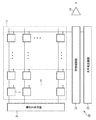
図7は、本実施形態による固体撮像装置の画素領域501のZ軸方向から見た平面図である。図7には、画素領域501を構成する3行×3列の画素回路401が示されているが、画素数は限定されないことは上述したとおりである。各画素回路401には、素子分離領域102により、略逆S字状の活性領域102aが画定されている。活性領域102a上には、画素回路を構成するトランジスタM1〜M6のゲート電極601〜606が配置されている。すなわち、図7における活性領域102aの下側から、複数のゲート電極601、602、603、604、605が、活性領域102aを横断するように、この順番で配置されている。ここで、ゲート電極601は第1の転送トランジスタM1のゲート電極であり、ゲート電極602は第2の転送トランジスタM2のゲート電極である。ゲート電極603はリセットトランジスタM3のゲート電極であり、ゲート電極604は増幅トランジスタM4のゲート電極である。ゲート電極605は選択トランジスタM5のゲート電極である。平面視において、ゲート電極604、605は隣り合っている。
FIG. 7 is a plan view of the
ゲート電極601の下側の活性領域102aは、フォトダイオードにより構成される光電変換部402である。ゲート電極601とゲート電極602との間の活性領域102aは、光電変換部402から転送される電荷を一時的に保持する電荷保持部403である。光電変換部402と電荷保持部403との間に配される第1の転送トランジスタM1が形成されている。ゲート電極602とゲート電極603との間の活性領域102aは、電荷電圧変換部404である。
The
活性領域102aは、光電変換部402と電源電圧線への接続部(ゲート電極603,604間の活性領域102a)との間で接続されており、この接続部上にOFDのトランジスタM6のゲート電極606が配置されている。電荷保持部403、ゲート電極601、602上には、遮光部材308が設けられている。図7において、黒の丸印は、上層の配線と接続するためのコンタクト部を模式的に表している。
The
図8は、本実施形態による固体撮像装置の画素領域および周辺領域の概略断面図である。すなわち、図8の左側の画素領域501は、図7のA−A’線の電荷保持部403から選択トランジスタM5に至る断面を示しており、点線よりも右側の周辺領域502は列増幅回路路等における隣接して設けられた任意の2つのトランジスタの断面を示している。図8には、X−Y平面に平行な断面図、Y−Z平面に平行な断面図が併せて示されている。
FIG. 8 is a schematic cross-sectional view of the pixel region and the peripheral region of the solid-state imaging device according to the present embodiment. That is, the
半導体基板100内には、P型半導体領域により構成されるウェル101と、素子分離領域102とが設けられている。画素領域501には、素子分離領域102により、図7に示すような略逆S字状の活性領域102aが画定されている。周辺領域502には、素子分離領域102により、活性領域102bが画定されている。
In the
画素領域501の活性領域102aの表面部には、N型半導体領域421およびP型半導体領域431、N型半導体領域422、N型半導体領域423、N型半導体領域424、N型半導体領域425が、互いに離間して設けられている。N型半導体領域421は、電荷保持部403を構成する不純物領域である。P型半導体領域431は、N型半導体領域421の表面保護層である。N型半導体領域422は、電荷電圧変換部404を構成する不純物領域(浮遊拡散領域)である。N型半導体領域423は、リセットトランジスタM3、増幅トランジスタM4のドレインを構成する不純物領域である。N型半導体領域424は、増幅トランジスタM4のソース、選択トランジスタM5のドレインを構成する不純物領域である。N型半導体領域425は、選択トランジスタM5のソースを構成する不純物領域であり、画素出力部407として機能する。
The N-
N型半導体領域421とN型半導体領域422との間の半導体基板100上には、ゲート絶縁膜103を介して、ゲート電極602が設けられている。これにより、N型半導体領域421、422により構成されるソース/ドレイン領域と、ゲート電極602とを有する第2の転送トランジスタM2が構成されている。また、N型半導体領域422とN型半導体領域423との間の半導体基板100上には、ゲート絶縁膜103を介して、ゲート電極603が設けられている。これにより、N型半導体領域422、423により構成されるソース/ドレイン領域と、ゲート電極603とを有するリセットトランジスタM3が構成されている。また、N型半導体領域423とN型半導体領域424との間の半導体基板100上には、ゲート絶縁膜103を介して、ゲート電極604が設けられている。これにより、N型半導体領域423、424により構成されるソース/ドレイン領域と、ゲート電極604とを有する増幅トランジスタM4が構成されている。また、N型半導体領域424とN型半導体領域425との間の半導体基板100上には、ゲート絶縁膜103を介して、ゲート電極605が設けられている。これにより、N型半導体領域424,425により構成されるソース/ドレイン領域と、ゲート電極605とを有する選択トランジスタM5が構成されている。
A
周辺領域502の活性領域102bの表面部には、N型半導体領域426、427、428が互いに離間して設けられている。N型半導体領域426とN型半導体領域427との間の半導体基板100上には、ゲート絶縁膜103を介して、ゲート電極607が設けられている。これにより、N型半導体領域426、427により構成されるソース/ドレイン領域と、ゲート電極607とを有する周辺トランジスタ617が構成される。また、N型半導体領域427とN型半導体領域428との間の半導体基板100上には、ゲート絶縁膜103を介して、ゲート電極608が設けられている。よって、N型半導体領域427、428により構成されるソース/ドレイン領域と、ゲート電極608とを有する周辺トランジスタ618が構成される。周辺トランジスタ617、618のN型半導体領域426、427、428、ゲート電極607、608の表面部には、配線抵抗、拡散層抵抗、コンタクト抵抗等を低減するための金属シリサイド膜432が設けられている。金属シリサイド膜432としては、コバルトシリサイドやチタンシリサイド等を適用可能である。
N-
画素領域501の半導体基板100上には、ゲート電極602、603、604、605の上面および側面を覆うように誘電体膜701、702が設けられている。誘電体膜701、702で覆われたゲート電極602、603、604、605の側面上には、サイドウォールスペーサ703a、704が設けられている。
周辺領域502に配置された周辺トランジスタ617、618の一対のゲート電極607、608の側面上には、サイドウォールスペーサ701aが設けられている。また、周辺領域502の半導体基板100上には、側面がサイドウォールスペーサ701aで覆われたゲート電極607、608の上面および側面を覆うように、誘電体膜703が設けられている。サイドウォールスペーサ701aおよび誘電体膜703で覆われたゲート電極607、608の側面上には、サイドウォールスペーサ704が設けられている。
半導体基板100上の全面には絶縁体膜301が設けられている。一対のゲート電極604、605の間隙は、絶縁体膜301によって埋め込まれておらず、ボイド801が形成されている。すなわち、第1および第2のゲート電極604、605、絶縁体膜301に囲まれた領域にボイド801が存在している。遮光部材308は平面視に垂直なZ軸方向において、ボイド801と絶縁体膜301を挟んで対向する位置には形成されていない。また、一対のゲート電極607、608の間隙は、絶縁体膜301によって埋め込まれておらず、ボイド802が形成されている。画素領域501の絶縁体膜301上には、電荷保持部403と第2の転送トランジスタM2のゲート電極602を覆うように、遮光部材308が設けられている。なお、図8には示されていないが、図2と同様に、絶縁体膜301上には、層間絶縁膜、層間絶縁膜および絶縁体膜301を貫通するコンタクトホール、コンタクトホールに接続された配線が設けられている。
An insulating
図9〜図11は、本実施形態による固体撮像装置の製造方法を示す工程断面図である。図9(a)において、半導体基板100の表面部に、例えばSTI法、LOCOS法等により、活性領域102a、102bを画定する素子分離領域102を形成する。次に、イオン注入法により、画素領域501および周辺領域502の所定の領域に、P型半導体領域で構成されるウェル101を形成する。イオン注入法により、画素領域501の電荷保持部403の形成領域に、N型半導体領域421およびP型半導体領域431を形成する。
9 to 11 are process cross-sectional views showing the method of manufacturing the solid-state imaging device according to the present embodiment. In FIG. 9A, the
半導体基板100の活性領域102a、102bの表面部に、例えば熱酸化法、CVD法を用いて、酸化シリコン膜等よりなるゲート絶縁膜103を形成する。ゲート絶縁膜103を形成した半導体基板100上の全面に、CVD法により、例えばポリシリコン膜を堆積する。次に、フォトリソグラフィおよびドライエッチングを用いて、ポリシリコン膜をパターニングし、ポリシリコン膜よりなるゲート電極602、603、604、605、607、608を形成する。イオン注入法により、画素領域501の半導体基板100内に、ゲート電極602、603、604、605に対して自己整合的に、N型半導体領域422、423、424、425を形成する。
A
なお、ここではゲート電極602〜608を形成する前にN型半導体領域421およびP型半導体領域431を形成する例を示しているが、ゲート電極602〜608を形成した後にN型半導体領域421およびP型半導体領域431を形成してもよい。この場合、N型半導体領域421およびP型半導体領域431は、N型半導体領域422、423、424,425と同様、ゲート電極602に対して自己整合的に形成することも可能である。
Although an example in which the N-
次に、ゲート電極602〜608が形成された半導体基板100上の全面に、CVD法等により、酸化シリコン膜等の誘電体膜701を形成する。誘電体膜701は、酸化シリコン層と窒化シリコン層との積層構造にすることで、反射防止膜として用いてもかまわない。フォトリソグラフィにより画素領域501を覆うとともに周辺領域502を露出するフォトレジスト膜(図示せず)を形成後、このフォトレジスト膜をマスクとして周辺領域502の誘電体膜701をエッチバックする。これにより、画素領域501に誘電体膜701を残すとともに、周辺領域502のゲート電極607、608の側面上に、誘電体膜701(第1の誘電体膜)よりなるサイドウォールスペーサ(第1のサイドウォールスペーサ)701aを形成する。次いで、例えばアッシングにより、マスクに用いたフォトレジスト膜(図示せず)を除去する。
Next, a
次に、図9(b)において、周辺領域502に、ゲート電極607、608およびサイドウォールスペーサ701aをマスクとしてイオン注入を行う。これにより、ゲート電極607、608およびサイドウォールスペーサ701aに対して自己整合的に、ソース/ドレイン領域となるN型半導体領域426、427、428を形成する。次いで、全面に、例えばCVD法等を用いて、誘電体膜702を成膜する。この誘電体膜702は、周辺領域502に金属シリサイド膜432を形成する際に画素領域501の保護膜として用いられる。誘電体膜702を成膜した後、フォトリソグラフィにより画素領域501を覆うとともに周辺領域502を露出するフォトレジスト膜(図示せず)を形成後、このフォトレジスト膜をマスクとして周辺領域502の誘電体膜702をエッチングする。これにより、誘電体膜702を、画素領域501に選択的に残存させる。次いで、例えばアッシングにより、マスクに用いたフォトレジスト膜(図示せず)を除去する。
Next, in FIG. 9B, ion implantation is performed on the
サリサイド(Self-ALIgned siliCIDE)プロセスにより、シリコンが露出している周辺領域502のゲート電極607、608およびN型半導体領域426の表面部に、金属シリサイド膜432を選択的に形成する。具体的には、例えばコバルト等の金属膜を堆積して熱処理を行い、この金属膜と接する部分のシリコンをシリサイド化した後、未反応の金属膜を除去する。これにより、金属シリサイド膜432が局所的に形成される。
A
次に、図10(a)に示されるように、全面に、例えばスパッタリング法、CVD法等を用いて、誘電体膜(第1の誘電体膜)703を成膜する。フォトリソグラフィにより周辺領域502を覆うとともに画素領域501を露出するフォトレジスト膜(図示せず)を形成後、このフォトレジスト膜をマスクとして画素領域501の誘電体膜703をエッチバックする。これにより、周辺領域502に誘電体膜703を残すとともに、誘電体膜701、702で覆われた画素領域501のゲート電極602〜605の側面上に、誘電体膜703よりなるサイドウォールスペーサ(第1のサイドウォールスペーサ)703aを形成する。次いで、例えばアッシングにより、マスクに用いたフォトレジスト膜(図示せず)を除去する。
Next, as shown in FIG. 10A, a dielectric film (first dielectric film) 703 is formed on the entire surface by, eg, sputtering or CVD. After forming a photoresist film (not shown) that covers the
次に、図10(b)に示されるように、全面に、例えばCVD法等を用いて、酸化シリコン膜等の第2の誘電体膜を成膜した後、この誘電体膜をエッチバックする。これにより、誘電体膜701、702、サイドウォールスペーサ703aで覆われたゲート電極602〜605の側面上に、サイドウォールスペーサ(第2のサイドウォールスペーサ)704を形成する。また、サイドウォールスペーサ701a、誘電体膜703で覆われたゲート電極607、608の側面上に、サイドウォールスペーサ704を形成する。この際、誘電体膜701、703を窒化シリコン膜とすることで、誘電体膜701、703をエッチングストッパ膜として用いてもよい。
Next, as shown in FIG. 10B, a second dielectric film such as a silicon oxide film is formed on the entire surface by, eg, CVD method, and then the dielectric film is etched back. .. Thus, sidewall spacers (second sidewall spacers) 704 are formed on the side surfaces of the
このとき、ゲート電極602〜608の側面を覆う膜の厚さとゲート電極602〜608間の間隔に応じて、サイドウォールスペーサ704間に狭い隙間が生じ、あるいは生じなくなる。例えば、ゲート電極602〜608の側面を覆う膜の厚さが0.2μmであるとすると、ゲート電極602〜608の間隔が0.3μmよりも狭い場合に、サイドウォールスペーサ704間に狭い隙間が発生する。このような狭い隙間は、例えば、隣り合う一対のゲート電極の間であって、これらゲート電極間の不純物領域にコンタクト部を設ける必要のない場所に発生し得る。例えば、図10(b)において、狭い隙間は、第1のゲート電極604および第2のゲート電極605の間と、第1のゲート電極607および第2のゲート電極608の間とにおいて発生している。ここで、狭い隙間に直接遮光部材308を成膜し、エッチングして取り除こうとすると、上述したように遮光部材308の残渣が発生する虞がある。後述するように、本実施形態によれば、狭い隙間にボイドを形成することで、エッチングの残渣の発生を防ぐことができる。なお、第1のゲート電極604と第2のゲート電極605との間の不純物領域には、図6に示すように、コンタクト部は設けられていない。一方、ゲート電極602〜608の間隔が0.4μmよりも大きい箇所には、このような狭い隙間は発生しない。
At this time, depending on the thickness of the film covering the side surfaces of the
次に、図11に示されるように、例えばプラズマCVD法等を用いて、酸化シリコン膜等の絶縁体膜301を成膜する。この際、第1のゲート電極604と第2のゲート電極605との間の空隙、および第1のゲート電極607と第2のゲート電極608との間の空隙において、絶縁体膜301が埋め込まれないように、ボイド801、802を形成する。ボイド801、802を残すように絶縁体膜301を形成することで、ゲート電極604、605間およびゲート電極607、608間の領域上の窪みが低減される。
Next, as shown in FIG. 11, an
具体的な成膜条件としては、TEOS−O2系やSiH4−O2系のガス種を用いた平行平板型プラズマCVD法など異方性や流動性の小さいCVD法を用いて成膜することが好ましい。これは、成膜速度が速くなることで、ゲート電極604とゲート電極605と絶縁体膜301との間に空隙であるボイド801が形成されやすくなる一方、ボイド801より十分狭い隙間が閉塞され、ボイド上の膜の窪みを低減することができるためである。
Specific film forming conditions, be formed by a TEOS-O2 system and SiH 4 -O parallel plate plasma CVD method small CVD method anisotropy and fluidity like using 2 based gas species Is preferred. This is because as the film formation speed increases,
本実施例では、ガス流量をTEOS:265sccm、O2:2.5sccmとし、圧力を360Paとした。また、RF出力を、上部電極720W、下部電極320Wとし、成膜時間を4secとして、500Å相当のプラズマCVD酸化膜を成膜した。 In this example, the gas flow rate was TEOS: 265 sccm, O 2 : 2.5 sccm, and the pressure was 360 Pa. Further, a plasma CVD oxide film equivalent to 500 Å was formed by setting RF output to the upper electrode 720W and the lower electrode 320W and forming the film for 4 seconds.
次に、絶縁体膜301上に、スパッタ法、CVD法等を用いて、タングステンまたはタングステンシリサイド等よりなる遮光部材308を形成する。さらに、フォトリソグラフィおよびドライエッチングを用いることにより、遮光部材308を所定の形状にパターニングする。
Next, a
パターニングによって、電荷保持部403、転送トランジスタのゲート電極601および第2の転送トランジスタ612のゲート電極602上における遮光部材308は残り、他の箇所はエッチングにより除去される。この際、ゲート電極604、605間、およびゲート電極607、608間の領域上の絶縁体膜301の表面の平坦性は、第1、第2実施形態と同様に向上し、この部分に遮光部材308のエッチング残渣が生じることを防ぐことができる。
By patterning, the light-shielding
また、ゲート電極602の側面上にサイドウォールスペーサ703a、704を積層することにより、ゲート電極602の段差を緩和することができる。これにより、遮光部材308の被覆性が向上し、遮光性能が向上する。さらに、増幅トランジスタM4の第1のゲート電極604と選択トランジスタM5の第2のゲート電極605の間には、ボイド801が形成される。空隙であるボイド801は、酸化シリコンや窒化シリコン等からなる誘電体膜703、704よりも誘電率が低い。このため、ゲート電極604、605間を誘電体膜703、704で埋め込む場合と比較してゲート電極604、605間の寄生容量を低減することができる。増幅トランジスタM4のゲート電極604の寄生容量が低減されることで、増幅回路の増幅効率の低下を抑制することができる。
Further, by stacking the
第1および第2実施形態と同様に、絶縁体膜301は遮光部材をエッチングする際にエッチストッパ膜としても機能する。Z軸方向(第1の方向)において、絶縁体膜301の膜厚をt、遮光部材308の膜厚をd1とし、遮光部材エッチング時のメインエッチ時間に対するオーバーエッチ時間の比をa、遮光部材エッチング時の遮光部材に対する絶縁体膜301のエッチング選択比をbとする。このとき、遮光部材エッチング時にエッチングされる絶縁体膜の厚さはa×b×d1である。
Similar to the first and second embodiments, the
絶縁体膜301の膜厚tがa×b×d1よりも薄いと、画素領域において遮光部材エッチング時に誘電体膜703の表面が露出する。誘電体膜703をフォトダイオードの反射防止膜として用いている場合、誘電体膜703がエッチングされて膜厚が変化すると、フォトダイオードの光学的特性が変化する恐れがある。そのため、絶縁体膜301の膜厚tはa×b×d1以上であることが好ましい。
When the film thickness t of the
誘電体膜703をフォトダイオードの反射防止膜として用いない場合は、絶縁体膜301の膜厚tと、誘電体膜703の膜厚t´の和がa×b×d1よりも薄ければよい。
When the
遮光部材308と配線が接触するとリークなどの原因となるため、絶縁体膜301の膜厚tは遮光部材と配線が接触しないような膜厚であることが好ましい。画素領域のゲート電極607〜608の膜厚が異なる場合には、大きい方のゲート電極の膜厚と、誘電体膜703の膜厚の和をd2、半導体基板100と配線との距離のうち最も小さい距離(層間絶縁膜の膜厚)をd3、ゲート絶縁膜103の厚さをd4としたとき、絶縁体膜301の膜厚tはd3−(d1+d2+d4)より薄いことが好ましい。
Since contact between the
遮光性の観点から、絶縁体膜301の膜厚は厚ければ厚いほど遮光部材308と半導体基板100との距離が広がり遮光性能が低下するため、絶縁体膜301の膜厚はできるだけ薄くするのが好ましい。
From the viewpoint of light shielding property, the thicker the insulating
具体的な例を以下に述べる。遮光部材308にタングステンを使用した場合、十分な遮光能力を得るためには、膜厚d1は0.1μm以上であることが好ましい。タングステンの透過率は0.1μm以上の厚さで0.2%以下となり十分な遮光能力を達成できる。
A specific example will be described below. When tungsten is used for the
遮光部材エッチング時のメインエッチ時間に対するオーバーエッチ時間の比aを0.1、遮光部材308に対する絶縁体膜301のエッチング選択比bが0.1であったとき、絶縁体膜301の膜厚tは少なくとも1nm以上である必要がある。実際は製造ばらつきなども考慮する必要があるため、絶縁体膜301の膜厚は5nm以上が好ましい。
When the ratio a of the over-etching time to the main etching time at the time of etching the light blocking member is 0.1 and the etching selection ratio b of the insulating
また、ゲート電極の膜厚d2を0.2μm、基板と配線との距離のうち最も小さい距離(層間絶縁膜の膜厚)d3を0.6μm、ゲート絶縁膜103の厚さを8.0nmとした場合、配線と接触しないためには絶縁体膜301の膜厚tは少なくとも0.3μmよりも薄くすることが好ましい。実際は層間絶縁膜厚、遮光部材308の膜厚の製造ばらつき、絶縁体膜301の膜厚tが厚くなることによる遮光性能の低下を考慮する必要があるため、実際の絶縁体膜301の膜厚tは0.1μmより小さいことが好ましい。
よって、絶縁体膜301の膜厚は、1nm以上かつ0.3μm未満であることが好ましく、より好ましくは、5nm以上かつ0.1μm未満であることが好ましい。
Further, the thickness d 2 of the gate electrode is 0.2 μm, the smallest distance (thickness of the interlayer insulating film) d 3 of the distance between the substrate and the wiring is 0.6 μm, and the thickness of the
Therefore, the thickness of the
このように、本実施形態によれば、ゲート電極の間に形成される絶縁体膜の表面の窪みを低減することができ、この領域上に形成される構造体の下地の平坦性を向上することができる。特に、ゲート電極間の領域上に形成される導電膜をエッチングにより除去する場合にあっては、絶縁体膜の窪みに導電膜の残渣を抑制し、製造歩留まりを向上させることができる。さらに、ゲート電極の側面上にサイドウォールスペーサを形成することにより、遮光性能を向上することができる。 As described above, according to this embodiment, it is possible to reduce the depressions on the surface of the insulator film formed between the gate electrodes, and improve the flatness of the base of the structure formed on this region. be able to. In particular, when the conductive film formed on the region between the gate electrodes is removed by etching, it is possible to suppress the residue of the conductive film in the recess of the insulating film and improve the manufacturing yield. Further, by forming the sidewall spacer on the side surface of the gate electrode, the light shielding performance can be improved.
本実施形態では、サイドウォールスペーサ間に狭い隙間が発生する条件として、ゲート電極間の間隔が0.3μmよりも狭い場合を例示したが、狭い隙間が発生するゲート電極間の間隔は、必ずしも0.3μmよりも狭い場合に限定されるものではない。ゲート電極の側面上に堆積される絶縁体膜の膜厚やサイドウォールスペーサの幅が変われば、これに応じてサイドウォールスペーサ間の隙間の幅も変わる。したがって、ボイドが残存するように絶縁体膜を形成する部位は、各固体撮像装置に求められるデザインルールやプロセス条件等に応じて、絶縁体膜上に形成される窪みの大きさを考慮しつつ、適宜設定することが好ましい。 In this embodiment, as an example of the condition that a narrow gap is generated between the sidewall spacers, the case where the gap between the gate electrodes is narrower than 0.3 μm is illustrated, but the gap between the gate electrodes where the narrow gap is generated is not always 0. It is not limited to the case of narrower than 0.3 μm. If the thickness of the insulator film deposited on the side surface of the gate electrode or the width of the sidewall spacers changes, the width of the gap between the sidewall spacers changes accordingly. Therefore, while considering the size of the depression formed on the insulator film, the portion where the insulator film is formed so that the voids remain remains in consideration of the design rules and process conditions required for each solid-state imaging device. It is preferable to set it appropriately.
また、本実施形態では、画素領域501のゲート電極601〜605を、誘電体膜701、702、サイドウォールスペーサ703a、704、絶縁体膜301で覆っている。しかし、ゲート電極601〜605を覆う絶縁体膜・誘電体膜の構成は、これに限定されるものではない。例えば、サイドウォールスペーサ703a、704による段差の緩和度合いに応じて、積層するサイドウォールスペーサの数を適宜増減してもよい。或いは、誘電体膜701、702のいずれかを形成しなくてもよい。周辺領域502についても同様である。
In this embodiment, the
さらに、本実施形態では、画素領域501における増幅トランジスタM4、選択トランジスタM5のゲート電極の間にボイドを形成する例を示したが、他のトランジスタM1〜M4、M6のゲート電極の間においてもボイドを形成しても良い。
Furthermore, in the present embodiment, an example is shown in which voids are formed between the gate electrodes of the amplification transistor M4 and the selection transistor M5 in the
(第4実施形態)
本発明の第4実施形態に係る撮像システムを説明する。撮像システムとして、デジタルスチルカメラ、デジタルカムコーダ、複写機、ファクシミリ、携帯電話、車載カメラ、観測衛星などがあげられる。図12に、第4実施形態に係る撮像システムの例としてデジタルスチルカメラのブロック図を示す。
(Fourth Embodiment)
An imaging system according to the fourth embodiment of the present invention will be described. Imaging systems include digital still cameras, digital camcorders, copiers, facsimiles, mobile phones, in-vehicle cameras, observation satellites, and the like. FIG. 12 shows a block diagram of a digital still camera as an example of the imaging system according to the fourth embodiment.
図12において、撮像システムは、レンズの保護のためのバリア1001、被写体の光学像を固体撮像装置1004に結像させるレンズ1002、レンズ1002を通った光量を可変するための絞り1003、メカニカルシャッタ1005を備える。撮像システムは上述の第1〜第3実施形態で説明した固体撮像装置1004をさらに備え、固体撮像装置1004はレンズ1002により結像された光学像を画像データとして変換する。ここで、固体撮像装置1004の半導体基板にはAD変換部が形成されているものとする。撮像システムはさらに信号処理部1007、タイミング発生部1008、全体制御・演算部1009、メモリ部1010、記録媒体制御I/F部1011、記録媒体1012、外部I/F部1013を備える。信号処理部1007は固体撮像装置1004より出力された撮像データに各種の補正やデータを圧縮する。タイミング発生部1008は固体撮像装置1004および信号処理部1007に各種タイミング信号を出力する。全体制御・演算部1009はデジタルスチルカメラ全体を制御し、メモリ部1010は画像データを一時的に記憶するためフレームメモリとして機能する。記録媒体制御I/F部1011は記録媒体に記録または読み出しを行う。記録媒体1012は着脱可能な半導体メモリ等から構成され、撮像データの記録または読み出しを行う。外部I/F部1013は外部コンピュータ等と通信するためのインターフェースである。ここで、タイミング信号などは撮像システムの外部から入力されてもよく、撮像システムは少なくとも固体撮像装置1004と、固体撮像装置1004から出力された撮像信号を処理する信号処理部1007とを有すればよい。
In FIG. 12, the imaging system includes a
(他の実施形態)
上述した実施形態は、本発明を実施するにあたっての具体例を示したものに過ぎず、これらによって本発明の技術的範囲が限定的に解釈されない。すなわち、本発明はその技術思想から逸脱することなく、様々な形で実施することができる。例えば、本発明は、トランジスタのゲート電極間の空隙のみならず、配線パターン間の微細スペースなど、遮光部材のエッチング残渣が生じる可能性のある回路構成に広く適用可能である。また、上述した実施形態では、信号電荷を電子とする固体撮像装置を例にして説明したが、本発明は、信号電荷を正孔とする固体撮像装置においても同様に適用することができる。なお、この場合、上述した半導体領域の導電型は、P型とN型とが逆になる。また、図6に示した固体撮像装置の画素回路の平面レイアウトは、一例を示したものであり、本発明を適用しうる固体撮像装置の画素回路の平面レイアウトは、これに限定されるものではない。さらに、画素回路の読み出し部の構成も、図6に示される例に限定されるものではない。
(Other embodiments)
The above-described embodiment merely shows specific examples for carrying out the present invention, and the technical scope of the present invention is not limitedly interpreted by these. That is, the present invention can be implemented in various forms without departing from the technical idea thereof. For example, the present invention can be widely applied not only to the space between the gate electrodes of the transistors but also to a circuit configuration in which an etching residue of the light shielding member may occur, such as a fine space between wiring patterns. Further, in the above-described embodiment, the solid-state imaging device having signal charges as electrons has been described as an example, but the present invention can be similarly applied to a solid-state imaging device having signal charges as holes. In this case, the conductivity type of the semiconductor region described above is opposite between the P type and the N type. The planar layout of the pixel circuit of the solid-state imaging device shown in FIG. 6 is an example, and the planar layout of the pixel circuit of the solid-state imaging device to which the present invention is applicable is not limited to this. Absent. Furthermore, the configuration of the readout unit of the pixel circuit is not limited to the example shown in FIG.
また、第3実施形態では、グローバル電子シャッタ機能を持つCMOSイメージセンサを例に挙げて本発明を説明したが、本発明を適用しうる固体撮像装置はCMOSイメージセンサに限定されるものではない。例えば、本発明は、CCDイメージセンサにも適用可能である。CCDイメージセンサでは、光電変換部における光電変換よって発生した電荷を読み出して転送するための読み出し部上に、遮光部材が配置される。この遮光部材が堆積される下地構造および製造方法に、上述の実施形態と同様の構造および製造方法を適用可能である。なお、本明細書において「電荷保持部」とは、固体撮像装置がCCDイメージセンサである場合においては、上述の読み出し部をも意味するものとする。 In addition, in the third embodiment, the present invention has been described by taking the CMOS image sensor having the global electronic shutter function as an example, but the solid-state imaging device to which the present invention can be applied is not limited to the CMOS image sensor. For example, the present invention can be applied to a CCD image sensor. In the CCD image sensor, a light shielding member is arranged on the reading unit for reading and transferring charges generated by photoelectric conversion in the photoelectric conversion unit. The same structure and manufacturing method as those of the above-described embodiments can be applied to the underlying structure and manufacturing method on which the light shielding member is deposited. In the present specification, the “charge holding unit” also means the above-mentioned reading unit when the solid-state imaging device is a CCD image sensor.
100 半導体基板
101 ウェル
102 素子分離領域
103 ゲート絶縁膜
201、202、601〜608 ゲート電極
203、204、205 不純物領域
301 絶縁体膜
303、701〜703 誘電体膜
302、801、802 ボイド
304〜307、701a、703a、704 サイドウォールスペーサ
308 遮光部材
421〜425 N型不純物領域
432 P型不純物領域
100
Claims (26)
第1の領域、第2の領域、第3の領域及び第4の領域を有する基板の上に、第1のトランジスタの第1のゲート電極と、前記第1のゲート電極に隣接する、第2のトランジスタの第2のゲート電極とを、前記第1のゲート電極が前記第1の領域の上に位置し、前記第2のゲート電極が前記第2の領域の上に位置し、前記第1のゲート電極と前記第2のゲート電極との間隙が前記第4の領域の上に位置するように形成する工程と、
前記第4の領域、前記第1のゲート電極及び前記第2のゲート電極を覆う絶縁体膜を成膜する工程と、
前記絶縁体膜の上に、前記第3の領域及び前記第4の領域を覆う遮光性の材料よりなる膜を成膜する工程と、
前記絶縁体膜を挟んでボイドの上に位置している前記遮光性の材料よりなる膜のうち、少なくとも前記第4の領域の上に位置する一部をエッチングで除去し、前記遮光性の材料よりなる膜から前記第3の領域の上に遮光部材を形成する工程と、
前記遮光部材、前記第1のゲート電極及び前記第2のゲート電極を覆う絶縁膜を形成する工程と、
前記絶縁膜を貫通して前記第1のトランジスタ及び前記第2のトランジスタのいずれかに接続するコンタクトプラグを形成する工程と、
前記絶縁膜の上に、前記コンタクトプラグに接続する配線を形成する工程と、
を有し、
前記遮光性の材料よりなる膜を成膜する工程において、前記絶縁体膜と前記第4の領域との間にボイドが存在する固体撮像装置の製造方法。 A method for manufacturing a solid-state imaging device, comprising:
A first gate electrode of a first transistor and a second gate electrode adjacent to the first gate electrode on a substrate having a first region, a second region, a third region and a fourth region. A second gate electrode of said transistor, said first gate electrode being located above said first region, said second gate electrode being located above said second region, said first gate electrode being located above said first region. Forming a gap between the gate electrode and the second gate electrode above the fourth region,
Forming an insulator film covering the fourth region, the first gate electrode and the second gate electrode;
Forming a film of a light-shielding material on the insulator film, the film covering the third region and the fourth region;
Of the film made of the light-shielding material located above the void with the insulator film interposed therebetween, at least a part of the film located above the fourth region is removed by etching, and the light-shielding material is formed. Forming a light blocking member on the third region from a film made of
Forming an insulating film covering the light shielding member, the first gate electrode and the second gate electrode;
Forming a contact plug penetrating the insulating film to connect to either the first transistor or the second transistor;
A step of forming a wiring connected to the contact plug on the insulating film,
Have
A method of manufacturing a solid-state imaging device, wherein a void exists between the insulator film and the fourth region in the step of forming a film made of the light-shielding material.
前記絶縁体膜が、a×b×d1≦tを満たすように形成される請求項1に記載の固体撮像装置の製造方法。 The ratio of the etching time of the insulating film to the etching time of the film of the light-shielding material is a, the etching selection ratio of the film of the light-shielding material to be the light-shielding member and the insulating film is b, When the thickness of the insulator film is t and the thickness of the light shielding member is d 1 ,
The method for manufacturing a solid-state imaging device according to claim 1, wherein the insulating film is formed so as to satisfy a×b×d 1 ≦t.
前記第1のトランジスタ及び前記第2のトランジスタは、前記周辺回路を構成する請求項1乃至3のいずれか1項に記載の固体撮像装置の製造方法。 The solid-state imaging device includes a peripheral circuit,
The method for manufacturing a solid-state imaging device according to claim 1, wherein the first transistor and the second transistor form the peripheral circuit.
前記画素回路は、
光電変換部からの電荷を電荷保持部に転送する第1の転送トランジスタと、
前記電荷保持部からの電荷を電荷電圧変換部に転送する第2の転送トランジスタと、
前記電荷電圧変換部の電位に応じた信号を出力する増幅トランジスタと、
を有し、
前記電荷保持部を含み、前記電荷保持部は前記遮光部材によって覆われている請求項1乃至4のいずれか1項に記載の固体撮像装置の製造方法。 The solid-state imaging device includes a pixel region having a plurality of pixel circuits,
The pixel circuit is
A first transfer transistor for transferring charges from the photoelectric conversion unit to the charge holding unit;
A second transfer transistor that transfers the charge from the charge holding unit to the charge-voltage conversion unit;
An amplification transistor that outputs a signal according to the potential of the charge-voltage converter,
Have
The method of manufacturing a solid-state imaging device according to claim 1, further comprising the charge holding portion, wherein the charge holding portion is covered with the light shielding member.
前記第1のゲート電極及び前記第2のゲート電極を覆う誘電体膜を成膜する工程と、
前記誘電体膜をエッチバックすることにより前記第1のゲート電極及び前記第2のゲート電極の側面上にサイドウォールスペーサを形成する工程と、
をさらに有する請求項1乃至6のいずれか1項に記載の固体撮像装置の製造方法。 Between the step of forming the first gate electrode and the second gate electrode and the step of forming the insulator film,
Forming a dielectric film covering the first gate electrode and the second gate electrode;
Forming sidewall spacers on side surfaces of the first gate electrode and the second gate electrode by etching back the dielectric film;
The method for manufacturing a solid-state imaging device according to claim 1, further comprising:
前記第1のゲート電極及び前記第2のゲート電極を覆う第1の誘電体膜を形成する工程と、
前記第1の誘電体膜をエッチングすることにより前記第1のゲート電極及び前記第2のゲート電極の側面上に第1のサイドウォールスペーサを形成する工程と、
前記第1のサイドウォールスペーサを覆う第2の誘電体膜を形成する工程と、
前記第2の誘電体膜をエッチングすることにより前記第1のサイドウォールスペーサの上に第2のサイドウォールスペーサを形成する工程と、
をさらに有する、請求項1乃至6のいずれか1項に記載の固体撮像装置の製造方法。 Between the step of forming the first gate electrode and the second gate electrode and the step of forming the insulator film,
Forming a first dielectric film covering the first gate electrode and the second gate electrode;
Forming a first sidewall spacer on a side surface of the first gate electrode and the second gate electrode by etching the first dielectric film;
Forming a second dielectric film covering the first sidewall spacers;
Forming a second sidewall spacer on the first sidewall spacer by etching the second dielectric film;
The method for manufacturing a solid-state imaging device according to claim 1, further comprising:
前記絶縁体膜を成膜する工程において、前記第1のサイドウォールスペーサと前記第2のサイドウォールスペーサとの間、前記絶縁体膜と前記第1のゲート電極の上面との間及び前記絶縁体膜と前記第2のゲート電極の上面との間に、前記第3の誘電体膜が位置する請求項8に記載の固体撮像装置の製造方法。 Between the step of forming the first sidewall spacer and the step of forming the second dielectric film, the first sidewall spacer, the first gate electrode, and the second gate electrode are covered. 3 further has a step of forming a dielectric film,
In the step of forming the insulator film, between the first sidewall spacer and the second sidewall spacer, between the insulator film and an upper surface of the first gate electrode, and the insulator. The method for manufacturing a solid-state imaging device according to claim 8, wherein the third dielectric film is located between a film and an upper surface of the second gate electrode.
前記第1の領域の上に位置する、第1のトランジスタの第1のゲート電極と、
前記第2の領域の上に位置し、前記第1のゲート電極に隣り合う、第2のトランジスタの第2のゲート電極と、
前記第3の領域、前記第4の領域、前記第1のゲート電極及び前記第2のゲート電極を覆う絶縁膜と、
前記絶縁膜と前記基板の間に配され、前記第3の領域、前記第4の領域、前記第1のゲート電極及び前記第2のゲート電極を覆う絶縁体膜と、
前記絶縁膜と前記第3の領域の間に設けられた遮光部材と、
前記絶縁膜の上に設けられた配線と、を備え、
前記絶縁体膜のうちの前記第3の領域を覆う部分が前記遮光部材と前記第3の領域の間に位置し、
前記第1のゲート電極と前記第2のゲート電極の間隙が前記第4の領域の上に位置し、前記絶縁体膜のうちの前記第4の領域を覆う部分と前記第4の領域の間にボイドが存在する、固体撮像装置。 A substrate having a first region, a second region, a third region and a fourth region,
A first gate electrode of a first transistor overlying the first region;
A second gate electrode of a second transistor located on the second region and adjacent to the first gate electrode;
An insulating film covering the third region, the fourth region, the first gate electrode and the second gate electrode,
An insulator film which is disposed between the insulating film and the substrate and covers the third region, the fourth region, the first gate electrode and the second gate electrode;
A light blocking member provided between the insulating film and the third region;
A wiring provided on the insulating film,
A portion of the insulating film covering the third region is located between the light blocking member and the third region,
Between the gap of the first gate electrode and the second gate electrode is located on the fourth region, said fourth region covering part and the fourth region of said insulator layer A solid-state imaging device in which a void exists.
前記ボイドは前記不純物領域の上に存在している請求項10乃至19のいずれか1項に記載の固体撮像装置。 The first transistor and the second transistor share an impurity region,
20. The solid-state imaging device according to claim 10, wherein the void exists on the impurity region.
光電変換部の電荷を電荷保持部に転送する第1の転送トランジスタと、
前記電荷保持部の電荷を電荷電圧変換部に転送する第2の転送トランジスタと、
前記電荷電圧変換部に接続されたゲート電極を有する第3トランジスタと、
を含み、
前記第1の転送トランジスタのゲート電極と、前記遮光部材は前記電荷保持部と、前記第2の転送トランジスタのゲート電極と、を覆う、請求項20に記載の固体撮像装置。 The pixel circuit is
A first transfer transistor for transferring charges of the photoelectric conversion unit to the charge holding unit;
A second transfer transistor for transferring the charge of the charge holding unit to the charge-voltage conversion unit;
A third transistor having a gate electrode connected to the charge-voltage converter,
Including
21. The solid-state imaging device according to claim 20, wherein the gate electrode of the first transfer transistor, the light shielding member covers the charge holding unit and the gate electrode of the second transfer transistor.
前記固体撮像装置が出力する信号を処理する信号処理部と、
を有する撮像システム。 A solid-state imaging device according to any one of claims 10 to 23,
A signal processing unit that processes a signal output by the solid-state imaging device;
Imaging system having.
前記CMOSイメージセンサが出力する信号を処理する信号処理部と、
を有する撮像システムであって、
前記CMOSイメージセンサは、
第1の領域、第2の領域、第3の領域及び第4の領域を有する基板と、
前記第1の領域の上に位置する、第1のトランジスタの第1のゲート電極と、
前記第2の領域の上に位置し、前記第1のゲート電極に隣り合う、第2のトランジスタの第2のゲート電極と、
前記第3の領域、前記第4の領域、前記第1のゲート電極及び前記第2のゲート電極を覆う絶縁膜と、
前記第3の領域、前記第4の領域、前記第1のゲート電極及び前記第2のゲート電極を覆う絶縁体膜と、
前記絶縁膜と前記第3の領域の間に設けられた遮光部材と、を備え、
前記絶縁膜と前記基板の間に配され、前記絶縁体膜のうちの前記第3の領域を覆う部分が前記遮光部材と前記第3の領域の間に位置し、
前記第1のゲート電極と前記第2のゲート電極の間の間隙が前記第4の領域の上に位置し、前記絶縁体膜のうちの前記第4の領域を覆う部分と前記第4の領域の間にボイドが存在する、撮像システム。 A CMOS image sensor having a global electronic shutter function,
A signal processing unit for processing a signal output from the CMOS image sensor;
An imaging system having:
The CMOS image sensor is
A substrate having a first region, a second region, a third region and a fourth region,
A first gate electrode of a first transistor overlying the first region;
A second gate electrode of a second transistor located on the second region and adjacent to the first gate electrode;
An insulating film covering the third region, the fourth region, the first gate electrode and the second gate electrode,
An insulator film covering the third region, the fourth region, the first gate electrode and the second gate electrode;
A light blocking member provided between the insulating film and the third region,
A portion of the insulator film, which is disposed between the insulating film and the substrate and covers the third region, is located between the light shielding member and the third region,
Said first gap between the gate electrode and the second gate electrode is located on the fourth region, said fourth region and said fourth region covering part of said insulator layer An imaging system in which there are voids between.
Priority Applications (4)
| Application Number | Priority Date | Filing Date | Title |
|---|---|---|---|
| US15/152,982 US9935140B2 (en) | 2015-05-19 | 2016-05-12 | Solid state imaging device, manufacturing method of solid state imaging device, and imaging system |
| CN201610320405.2A CN106169489B (en) | 2015-05-19 | 2016-05-16 | The manufacturing method and imaging system of solid-state imaging apparatus, solid-state imaging apparatus |
| EP16170126.3A EP3096355B1 (en) | 2015-05-19 | 2016-05-18 | Solid state imaging device, manufacturing method of solid state imaging device, and imaging system |
| US15/897,940 US10381389B2 (en) | 2015-05-19 | 2018-02-15 | Solid state imaging device, manufacturing method of solid state imaging device, and imaging system |
Applications Claiming Priority (2)
| Application Number | Priority Date | Filing Date | Title |
|---|---|---|---|
| JP2015101704 | 2015-05-19 | ||
| JP2015101704 | 2015-05-19 |
Publications (3)
| Publication Number | Publication Date |
|---|---|
| JP2016219792A JP2016219792A (en) | 2016-12-22 |
| JP2016219792A5 JP2016219792A5 (en) | 2019-05-23 |
| JP6727897B2 true JP6727897B2 (en) | 2020-07-22 |
Family
ID=57578618
Family Applications (1)
| Application Number | Title | Priority Date | Filing Date |
|---|---|---|---|
| JP2016081833A Active JP6727897B2 (en) | 2015-05-19 | 2016-04-15 | Solid-state imaging device, method of manufacturing solid-state imaging device, and imaging system |
Country Status (1)
| Country | Link |
|---|---|
| JP (1) | JP6727897B2 (en) |
Families Citing this family (4)
| Publication number | Priority date | Publication date | Assignee | Title |
|---|---|---|---|---|
| JP6957226B2 (en) * | 2017-06-20 | 2021-11-02 | キヤノン株式会社 | Photoelectric converters and equipment |
| JP2019075441A (en) * | 2017-10-13 | 2019-05-16 | キヤノン株式会社 | Photoelectric conversion device and equipment |
| KR102538174B1 (en) | 2017-12-26 | 2023-05-31 | 삼성전자주식회사 | Semiconductor device including via plug |
| KR102051752B1 (en) * | 2018-06-14 | 2020-01-09 | 매그나칩 반도체 유한회사 | Semiconductor Device and Method for Manufacturing Thereof |
Family Cites Families (12)
| Publication number | Priority date | Publication date | Assignee | Title |
|---|---|---|---|---|
| JPH11274300A (en) * | 1998-03-23 | 1999-10-08 | Nkk Corp | Manufacturing semiconductor element |
| JP2000150857A (en) * | 1998-11-18 | 2000-05-30 | Nec Corp | Solid-state imaging device and manufacture of it |
| JP2000216371A (en) * | 1999-01-26 | 2000-08-04 | Matsushita Electronics Industry Corp | Charge transfer device, and its manufacture |
| JP3782297B2 (en) * | 2000-03-28 | 2006-06-07 | 株式会社東芝 | Solid-state imaging device and manufacturing method thereof |
| JP2003282853A (en) * | 2002-03-27 | 2003-10-03 | Matsushita Electric Ind Co Ltd | Solid state imaging device, method for manufacturing the same, and method for manufacturing semiconductor device |
| JP4340248B2 (en) * | 2005-03-17 | 2009-10-07 | 富士通マイクロエレクトロニクス株式会社 | Method for manufacturing a semiconductor imaging device |
| JP2006295071A (en) * | 2005-04-14 | 2006-10-26 | Toshiba Corp | Semiconductor device manufacturing method |
| JP4993007B2 (en) * | 2010-07-26 | 2012-08-08 | 富士通セミコンダクター株式会社 | Solid-state imaging device |
| JP2012182426A (en) * | 2011-02-09 | 2012-09-20 | Canon Inc | Solid state image pickup device, image pickup system using solid state image pickup device and solis state image pickup device manufacturing method |
| JP5814625B2 (en) * | 2011-05-27 | 2015-11-17 | キヤノン株式会社 | Solid-state imaging device, imaging system using the same, and method for manufacturing solid-state imaging device |
| JP2013110285A (en) * | 2011-11-22 | 2013-06-06 | Sony Corp | Solid-state imaging device, manufacturing method and electronic apparatus |
| JP2014022421A (en) * | 2012-07-13 | 2014-02-03 | Sony Corp | Solid-state imaging element, method for manufacturing the same, and electronic device |
-
2016
- 2016-04-15 JP JP2016081833A patent/JP6727897B2/en active Active
Also Published As
| Publication number | Publication date |
|---|---|
| JP2016219792A (en) | 2016-12-22 |
Similar Documents
| Publication | Publication Date | Title |
|---|---|---|
| JP4340248B2 (en) | Method for manufacturing a semiconductor imaging device | |
| JP5305622B2 (en) | Method for manufacturing photoelectric conversion device | |
| JP5812692B2 (en) | Method for manufacturing solid-state imaging device | |
| JP5814625B2 (en) | Solid-state imaging device, imaging system using the same, and method for manufacturing solid-state imaging device | |
| US8298851B2 (en) | Method of manufacturing a solid-state imaging device with a silicide blocking layer and electronic apparatus | |
| JP2014199898A (en) | Solid-state imaging element and method of manufacturing the same, and electronic equipment | |
| JP4490407B2 (en) | CMOS image sensor and manufacturing method thereof | |
| JP2005347325A (en) | Solid-state imaging device and its manufacturing method | |
| JP2013110285A (en) | Solid-state imaging device, manufacturing method and electronic apparatus | |
| JP6727897B2 (en) | Solid-state imaging device, method of manufacturing solid-state imaging device, and imaging system | |
| JP4486043B2 (en) | CMOS image sensor and manufacturing method thereof | |
| US10381389B2 (en) | Solid state imaging device, manufacturing method of solid state imaging device, and imaging system | |
| JP6711597B2 (en) | Solid-state imaging device manufacturing method, solid-state imaging device, and imaging system having the same | |
| US8368161B2 (en) | Solid-state image capturing device, method of manufacturing solid-state image capturing device, and image capturing apparatus | |
| KR102067296B1 (en) | Solid-state imaging element and electronic device | |
| US9608033B2 (en) | Solid-state image sensor, method of manufacturing the same, and camera | |
| JP2006024786A (en) | Solid-state imaging device and its manufacturing method | |
| US10461119B2 (en) | Solid-state imaging device, imaging system, and method for manufacturing solid-state imaging device | |
| TWI525801B (en) | Image sensor with doped transfer gate | |
| JP5700945B2 (en) | Photoelectric conversion device and manufacturing method thereof | |
| JP5240146B2 (en) | Solid-state image sensor | |
| JP6039773B2 (en) | Method for manufacturing solid-state imaging device | |
| KR20090111292A (en) | Solid-state imaging device and method of manufacturing the same and electronic apparatus |
Legal Events
| Date | Code | Title | Description |
|---|---|---|---|
| RD05 | Notification of revocation of power of attorney |
Free format text: JAPANESE INTERMEDIATE CODE: A7425 Effective date: 20171214 |
|
| RD04 | Notification of resignation of power of attorney |
Free format text: JAPANESE INTERMEDIATE CODE: A7424 Effective date: 20180126 |
|
| A521 | Written amendment |
Free format text: JAPANESE INTERMEDIATE CODE: A523 Effective date: 20190411 |
|
| A621 | Written request for application examination |
Free format text: JAPANESE INTERMEDIATE CODE: A621 Effective date: 20190411 |
|
| A977 | Report on retrieval |
Free format text: JAPANESE INTERMEDIATE CODE: A971007 Effective date: 20200213 |
|
| A131 | Notification of reasons for refusal |
Free format text: JAPANESE INTERMEDIATE CODE: A131 Effective date: 20200317 |
|
| A521 | Written amendment |
Free format text: JAPANESE INTERMEDIATE CODE: A523 Effective date: 20200515 |
|
| TRDD | Decision of grant or rejection written | ||
| A01 | Written decision to grant a patent or to grant a registration (utility model) |
Free format text: JAPANESE INTERMEDIATE CODE: A01 Effective date: 20200602 |
|
| A61 | First payment of annual fees (during grant procedure) |
Free format text: JAPANESE INTERMEDIATE CODE: A61 Effective date: 20200701 |
|
| R151 | Written notification of patent or utility model registration |
Ref document number: 6727897 Country of ref document: JP Free format text: JAPANESE INTERMEDIATE CODE: R151 |