JP6726558B2 - Substrate processing method, substrate processing apparatus, and recording medium - Google Patents
Substrate processing method, substrate processing apparatus, and recording medium Download PDFInfo
- Publication number
- JP6726558B2 JP6726558B2 JP2016152862A JP2016152862A JP6726558B2 JP 6726558 B2 JP6726558 B2 JP 6726558B2 JP 2016152862 A JP2016152862 A JP 2016152862A JP 2016152862 A JP2016152862 A JP 2016152862A JP 6726558 B2 JP6726558 B2 JP 6726558B2
- Authority
- JP
- Japan
- Prior art keywords
- unit
- coating
- photosensitizer
- acid
- wafer
- Prior art date
- Legal status (The legal status is an assumption and is not a legal conclusion. Google has not performed a legal analysis and makes no representation as to the accuracy of the status listed.)
- Active
Links
Images


Classifications
-
- H—ELECTRICITY
- H10—SEMICONDUCTOR DEVICES; ELECTRIC SOLID-STATE DEVICES NOT OTHERWISE PROVIDED FOR
- H10P—GENERIC PROCESSES OR APPARATUS FOR THE MANUFACTURE OR TREATMENT OF DEVICES COVERED BY CLASS H10
- H10P76/00—Manufacture or treatment of masks on semiconductor bodies, e.g. by lithography or photolithography
- H10P76/20—Manufacture or treatment of masks on semiconductor bodies, e.g. by lithography or photolithography of masks comprising organic materials
- H10P76/204—Manufacture or treatment of masks on semiconductor bodies, e.g. by lithography or photolithography of masks comprising organic materials of organic photoresist masks
- H10P76/2041—Photolithographic processes
-
- G—PHYSICS
- G03—PHOTOGRAPHY; CINEMATOGRAPHY; ANALOGOUS TECHNIQUES USING WAVES OTHER THAN OPTICAL WAVES; ELECTROGRAPHY; HOLOGRAPHY
- G03F—PHOTOMECHANICAL PRODUCTION OF TEXTURED OR PATTERNED SURFACES, e.g. FOR PRINTING, FOR PROCESSING OF SEMICONDUCTOR DEVICES; MATERIALS THEREFOR; ORIGINALS THEREFOR; APPARATUS SPECIALLY ADAPTED THEREFOR
- G03F7/00—Photomechanical, e.g. photolithographic, production of textured or patterned surfaces, e.g. printing surfaces; Materials therefor, e.g. comprising photoresists; Apparatus specially adapted therefor
- G03F7/20—Exposure; Apparatus therefor
-
- G—PHYSICS
- G03—PHOTOGRAPHY; CINEMATOGRAPHY; ANALOGOUS TECHNIQUES USING WAVES OTHER THAN OPTICAL WAVES; ELECTROGRAPHY; HOLOGRAPHY
- G03F—PHOTOMECHANICAL PRODUCTION OF TEXTURED OR PATTERNED SURFACES, e.g. FOR PRINTING, FOR PROCESSING OF SEMICONDUCTOR DEVICES; MATERIALS THEREFOR; ORIGINALS THEREFOR; APPARATUS SPECIALLY ADAPTED THEREFOR
- G03F7/00—Photomechanical, e.g. photolithographic, production of textured or patterned surfaces, e.g. printing surfaces; Materials therefor, e.g. comprising photoresists; Apparatus specially adapted therefor
- G03F7/26—Processing photosensitive materials; Apparatus therefor
- G03F7/40—Treatment after imagewise removal, e.g. baking
Landscapes
- Physics & Mathematics (AREA)
- General Physics & Mathematics (AREA)
- Exposure Of Semiconductors, Excluding Electron Or Ion Beam Exposure (AREA)
- Photosensitive Polymer And Photoresist Processing (AREA)
- Exposure And Positioning Against Photoresist Photosensitive Materials (AREA)
- Materials For Photolithography (AREA)
Description
本開示は、基板処理方法、基板処理装置及び記録媒体に関する。 The present disclosure relates to a substrate processing method, a substrate processing apparatus, and a recording medium.
特許文献1には、シリコンウェハ上にレジスト膜を形成した後、レジスト膜に所望パターンを露光し、次いでレジスト膜がポジパターンを得るようなアルカリ現像液を用いて現像し、次いでレジスト膜がネガパターンを得るような有機溶剤を用いて現像するレジストパターン形成方法が開示されている。 In Patent Document 1, after forming a resist film on a silicon wafer, a desired pattern is exposed on the resist film, followed by development using an alkali developing solution so that the resist film obtains a positive pattern, and then the resist film is negative. A resist pattern forming method is disclosed in which development is performed by using an organic solvent that obtains a pattern.
本開示は、フォトリソグラフィーによるパターンの微細化に有効な基板処理方法、基板処理装置及び記録媒体を提供することを目的とする。 An object of the present disclosure is to provide a substrate processing method, a substrate processing apparatus, and a recording medium which are effective for pattern miniaturization by photolithography.
本開示に係る基板処理方法は、第一露光処理によって光増感剤を発生させる第一成分と、光増感剤からのエネルギーの供給に応じて酸を発生させる第二成分とを含む被膜を基板の表面に形成する被膜形成処理と、第一露光処理にて発生した光増感剤から第二成分にエネルギーを供給して酸を発生させるように、光増感剤を励起するための光を被膜に照射する第二露光処理と、第二露光処理にて発生した酸による触媒反応を促進するように被膜を加熱する第一加熱処理と、第一加熱処理における触媒反応が生じた箇所を溶解させる第一現像液を被膜に供給する第一現像処理と、第一現像処理の後に、被膜内に残留した光増感剤から第二成分にエネルギーを供給して酸を発生させるように、光増感剤を励起するための光を被膜に照射する第三露光処理と、第三露光処理にて発生した酸による触媒反応を促進するように被膜を加熱する第二加熱処理と、第二加熱処理における触媒反応が生じていない箇所を溶解させる第二現像液を被膜に供給する第二現像処理と、を含む。 The substrate processing method according to the present disclosure provides a coating film including a first component that generates a photosensitizer by the first exposure treatment and a second component that generates an acid in response to the supply of energy from the photosensitizer. Light for exciting the photosensitizer so that a film is formed on the surface of the substrate and the photosensitizer generated in the first exposure process supplies energy to the second component to generate an acid. The second exposure treatment for irradiating the coating with, the first heat treatment for heating the coating so as to promote the catalytic reaction by the acid generated in the second exposure treatment, and the portion where the catalytic reaction occurs in the first heat treatment. A first developing treatment for supplying a first developing solution to be dissolved to the coating, and after the first developing treatment, energy is generated from the photosensitizer remaining in the coating to the second component to generate an acid, A third exposure treatment of irradiating the coating with light for exciting the photosensitizer, a second heat treatment of heating the coating so as to promote a catalytic reaction by an acid generated in the third exposure treatment, and a second A second developing treatment in which a second developing solution that dissolves a portion in which a catalytic reaction has not occurred in the heat treatment is supplied to the coating film.
この基板処理方法によれば、酸による触媒反応(以下、「酸触媒反応」という。)が生じた箇所を溶解させる第一現像処理を行うことで得られたパターン(以下、「第一パターン」という。)に対し、酸触媒反応が生じていない箇所を溶解させる第二現像処理を更に行うことで、第一パターンを更に細分化したパターン(以下、「第二パターン」という。)が得られる。 According to this substrate processing method, a pattern (hereinafter, referred to as “first pattern”) obtained by performing a first development process for dissolving a portion where a catalytic reaction by an acid (hereinafter, referred to as “acid catalytic reaction”) is dissolved. The second development treatment for dissolving the portion in which the acid-catalyzed reaction has not occurred is further performed to obtain a pattern in which the first pattern is further subdivided (hereinafter, referred to as “second pattern”). ..
第一現像処理は、第二露光処理及び第一加熱処理の後に行われる。第二露光処理では、第一露光処理において露光された領域(以下、「第一領域」という。)の光増感剤が励起され、励起された光増感剤から第二成分にエネルギーが供給されることで、第一領域の酸が増殖する。第一加熱処理では、酸触媒反応が加熱によって促進される。第二露光処理により第一領域の酸が増殖しているので、第一加熱処理においては酸触媒反応が効率よく進行する。このため、被膜の過剰な加熱による溶解を抑制しつつ、酸触媒反応を促進することができる。酸触媒反応の促進により、第一領域とその他の領域とで、第一現像液に対する溶解性の差異が顕著になるので、第一パターンを高い信頼性で形成できる。 The first development process is performed after the second exposure process and the first heating process. In the second exposure process, the photosensitizer in the region exposed in the first exposure process (hereinafter referred to as “first region”) is excited, and energy is supplied from the excited photosensitizer to the second component. As a result, the acid in the first region grows. In the first heat treatment, the acid-catalyzed reaction is accelerated by heating. Since the acid in the first region is grown by the second exposure treatment, the acid-catalyzed reaction proceeds efficiently in the first heat treatment. Therefore, the acid-catalyzed reaction can be promoted while suppressing the dissolution of the coating film due to excessive heating. By promoting the acid-catalyzed reaction, the difference in solubility in the first developer between the first region and the other regions becomes noticeable, so that the first pattern can be formed with high reliability.
第二現像処理は、第三露光処理及び第二加熱処理の後に行われる。第三露光処理では、第一パターンのうち光増感剤が残留している領域(以下、「第二領域」という。)の酸が増殖する。第二加熱処理では、酸触媒反応が加熱によって促進される。第三露光処理により第二領域の酸が増殖しているので、第二加熱処理においても酸触媒反応が効率よく進行する。このため、被膜の過剰な加熱による溶解を抑制しつつ、酸触媒反応を促進することができる。酸触媒反応の促進により、第二領域とその他の領域とで、第二現像液に対する溶解性の差異が顕著になるので、第二パターンも高い信頼性で形成できる。 The second development process is performed after the third exposure process and the second heating process. In the third exposure process, the acid in the region where the photosensitizer remains in the first pattern (hereinafter, referred to as “second region”) grows. In the second heat treatment, the acid-catalyzed reaction is accelerated by heating. Since the acid in the second region is proliferated by the third exposure treatment, the acid-catalyzed reaction efficiently proceeds even in the second heat treatment. Therefore, the acid-catalyzed reaction can be promoted while suppressing the dissolution of the coating film due to excessive heating. By promoting the acid-catalyzed reaction, the difference in solubility in the second developing solution becomes remarkable between the second region and the other regions, so that the second pattern can be formed with high reliability.
従って、フォトリソグラフィーによるパターンの微細化に有効である。 Therefore, it is effective for pattern miniaturization by photolithography.
第二加熱処理では、第一加熱処理に比較して低い温度にて被膜を加熱してもよい。この場合、第二加熱処理における被膜の過剰な加熱が更に抑制されるので、第二パターンを更に高い信頼性で形成できる。 In the second heat treatment, the coating may be heated at a temperature lower than that in the first heat treatment. In this case, since excessive heating of the coating film in the second heat treatment is further suppressed, the second pattern can be formed with higher reliability.
第一現像液はアルカリ現像液であり、第二現像液は有機現像液であってもよい。光増感剤はカルボニル化合物を含有してもよい。 The first developer may be an alkaline developer and the second developer may be an organic developer. The photosensitizer may contain a carbonyl compound.
本開示に係る基板処理装置は、上記基板処理方法を実行するための装置であって、被膜を基板の表面に形成する被膜形成部と、光増感剤を励起するための光を被膜に照射する光照射部と、被膜を加熱する加熱部と、被膜に第一現像液を供給する第一現像液供給部と、被膜に第二現像液を供給する第二現像液供給部と、を備える。 A substrate processing apparatus according to the present disclosure is an apparatus for performing the above substrate processing method, and irradiates the film with a film forming unit that forms a film on the surface of a substrate and light for exciting a photosensitizer. And a heating unit for heating the film, a first developer supplying unit for supplying the first developing solution to the film, and a second developing solution supplying unit for supplying the second developing solution to the film. ..
本開示に係る記録媒体は、上記基板処理方法を装置に実行させるためのプログラムを記録した、コンピュータ読み取り可能な記録媒体である。 A recording medium according to the present disclosure is a computer-readable recording medium in which a program for causing the apparatus to execute the substrate processing method is recorded.
本開示によれば、フォトリソグラフィーによるパターンの微細化に有効な基板処理方法、基板処理装置及び記録媒体を提供することができる。 According to the present disclosure, it is possible to provide a substrate processing method, a substrate processing apparatus, and a recording medium that are effective for pattern miniaturization by photolithography.
以下、実施形態について図面を参照しつつ詳細に説明する。説明において、同一要素又は同一機能を有する要素には同一の符号を付し、重複する説明を省略する。 Hereinafter, embodiments will be described in detail with reference to the drawings. In the description, the same elements or elements having the same function will be denoted by the same reference symbols, without redundant description.
〔基板処理システム〕
基板処理システム1は、基板に対し、被膜の形成、当該被膜の露光、及び当該被膜の現像を施すシステムである。処理対象の基板は、例えば半導体のウェハWである。被膜は、例えば感光性のレジスト膜を含む。
[Substrate processing system]
The substrate processing system 1 is a system that forms a film on a substrate, exposes the film, and develops the film. The substrate to be processed is, for example, a semiconductor wafer W. The coating includes, for example, a photosensitive resist film.
基板処理システム1は、塗布・現像装置2と露光装置3とを備える。露光装置3は、ウェハWの表面に形成されたレジスト膜の露光処理を行う。具体的には、液浸露光等の方法によりレジスト膜の露光対象部分にエネルギー線を照射する。塗布・現像装置2は、露光装置3による露光処理の前に、ウェハWの表面にレジスト膜を形成する処理を行い、露光処理後にレジスト膜の現像処理を行う。
The substrate processing system 1 includes a coating/developing
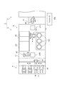
(塗布・現像装置)
以下、基板処理装置の一例として、塗布・現像装置2の構成を説明する。図1〜図3に示すように、塗布・現像装置2は、キャリアブロック4と、処理ブロック5と、インタフェースブロック6と、コントローラ100とを備える。
(Coating/developing device)
The configuration of the coating/developing
キャリアブロック4は、塗布・現像装置2内へのウェハWの導入及び塗布・現像装置2内からのウェハWの導出を行う。例えばキャリアブロック4は、ウェハW用の複数のキャリア11を支持可能であり、受け渡しアームA1を内蔵している。キャリア11は、例えば円形の複数枚のウェハWを収容する。受け渡しアームA1は、キャリア11からウェハWを取り出して処理ブロック5に渡し、処理ブロック5からウェハWを受け取ってキャリア11内に戻す。
The carrier block 4 introduces the wafer W into the coating/developing
処理ブロック5は、複数の処理モジュール14,15,16,17を有する。図2及び図3に示すように、処理モジュール14,15,16,17は、複数の液処理ユニットU1と、複数の熱処理ユニットU2と、これらのユニットにウェハWを搬送する搬送アームA3とを内蔵している。液処理ユニットU1は、処理液をウェハWの表面に塗布する。熱処理ユニットU2は、例えば熱板及び冷却板を内蔵しており、熱板によりウェハWを加熱し、加熱後のウェハWを冷却板により冷却して熱処理を行う。
The processing block 5 has a plurality of
処理モジュール14,15,16(被膜形成部)は、ウェハWの表面Waに上記被膜を形成する。被膜は、ウェハWの表面Wa上に形成される下層膜と、下層膜上に形成される感光性のレジスト膜と、レジスト膜上に形成される上層膜とを含む。なお、被膜は少なくともレジスト膜を含んでいればよいので、例えば被膜は下層膜を含んでいなくてもよく、上層膜を含んでいなくてもよく、下層膜及び上層膜の両方を含んでいなくてもよい。
The
処理モジュール14は、液処理ユニットU1及び熱処理ユニットU2によりウェハWの表面上に下層膜を形成する。処理モジュール14の液処理ユニットU1は、下層膜形成用の処理液をウェハW上に塗布する。処理モジュール14の熱処理ユニットU2は、下層膜の形成に伴う各種熱処理を行う。
The
処理モジュール15は、液処理ユニットU1及び熱処理ユニットU2により下層膜上にレジスト膜を形成する。
The
レジスト膜は、ベース材料と、露光装置3における露光処理(第一露光処理)によって光増感剤を発生させる第一成分と、光増感剤からのエネルギーの供給に応じて酸を発生させる第二成分とを含む。露光装置3における露光処理によって発生する光増感剤は、カルボニル化合物を含有してもよい。
The resist film is a base material, a first component that generates a photosensitizer by an exposure process (first exposure process) in the
ベース材料の具体例としては、重量平均分子量が1000〜200000である高分子化合物であって、酸触媒反応により、後述の現像液に対して可溶又は不溶となるものが挙げられる。ベース材料の重量平均分子量は、2000〜50000であってもよく、2000〜20000であってもよい。 Specific examples of the base material include high molecular weight compounds having a weight average molecular weight of 1,000 to 200,000, which are soluble or insoluble in a developing solution described below due to an acid-catalyzed reaction. The weight average molecular weight of the base material may be 2000 to 50000, or 2000 to 20000.
例えばベース材料は、極性基(例えば、酸性官能基)が酸不安定基で保護された高分子化合物である。このような高分子化合物は有機現像液に可溶であるが、アルカリ現像液には不溶又は難溶である。上記極性基が酸不安定基で保護された高分子化合物は、酸による触媒反応(以下、「酸触媒反応」ともいう。)によって酸不安定基が外れ(脱保護)、極性が付与され、アルカリ現像液に可溶であるが、有機現像液に不溶又は難溶となる。この場合、レジスト膜のうち酸触媒反応が生じていない部分は有機現像液により除去可能となり、酸触媒反応が生じた部分はアルカリ現像液により除去可能となる。すなわち、このような高分子化合物をベース材料として含むレジスト膜を有機現像液にて現像する場合、当該レジスト膜はネガ型レジストとして働き、当該レジスト膜をアルカリ現像液にて現像する場合、当該レジスト材料はポジ型レジスト材料として働く。 For example, the base material is a polymer compound in which a polar group (for example, an acidic functional group) is protected by an acid labile group. Such a polymer compound is soluble in an organic developing solution but insoluble or hardly soluble in an alkaline developing solution. In the polymer compound in which the polar group is protected with an acid labile group, the acid labile group is removed (deprotected) by a catalytic reaction with an acid (hereinafter, also referred to as “acid catalyzed reaction”), and polarity is imparted. It is soluble in alkaline developers but insoluble or poorly soluble in organic developers. In this case, the portion of the resist film where the acid catalyst reaction has not occurred can be removed with the organic developer, and the portion where the acid catalyst reaction has occurred can be removed with the alkali developer. That is, when a resist film containing such a polymer compound as a base material is developed with an organic developer, the resist film acts as a negative resist, and when the resist film is developed with an alkali developer, the resist film is The material acts as a positive resist material.
ベース材料のより具体的な例としては、フェノール樹脂、(メタ)アクリル樹脂、ポリビニルアセタール樹脂、ポリウレタン樹脂、ポリアミド樹脂、エポキシ樹脂、スチレン系樹脂、及びポリエステル樹脂等が挙げられる。高分子化合物は、フェノール樹脂、(メタ)アクリル樹脂、又はスチレン系樹脂であってもよく、(メタ)アクリル樹脂であってもよい。 More specific examples of the base material include phenol resin, (meth)acrylic resin, polyvinyl acetal resin, polyurethane resin, polyamide resin, epoxy resin, styrene resin, and polyester resin. The polymer compound may be a phenol resin, a (meth)acrylic resin, a styrene resin, or a (meth)acrylic resin.
第一成分の具体例としては、光増感剤前駆体が挙げられる。光増感剤前駆体は、露光装置3における露光処理によって光増感剤となる。例えば、光増感剤前駆体は、電離放射線又は400nm以下の波長を有する非電離放射線の照射によって光増感剤となる。光増感剤前駆体は、250nm以下の波長を有する非電離放射線の照射によって光増感剤となるものであってもよく、200nm以下の波長を有する非電離放射線の照射によって光増感剤となるものであってもよい。
Specific examples of the first component include a photosensitizer precursor. The photosensitizer precursor becomes a photosensitizer by the exposure process in the
光増感剤は、200nmを超える波長を有する非電離放射線によって励起されるものであってもよく、250nmを超える波長を有する非電離放射線によって励起されるものであってもよい。光増感剤を励起するための非電離放射線の波長は、光増感剤前駆体を光増感剤に変化させるための非電離放射線の波長に比較して長くてもよい。 The photosensitizer may be one that is excited by non-ionizing radiation having a wavelength of more than 200 nm, or one that is excited by non-ionizing radiation having a wavelength of more than 250 nm. The wavelength of non-ionizing radiation for exciting the photosensitizer may be longer than the wavelength of non-ionizing radiation for converting the photosensitizer precursor into a photosensitizer.
光増感剤前駆体は、カルボニル基を有する化合物(カルボニル化合物)を含有する光増感剤となるものであってもよい。カルボニル化合物としてはアルデヒド及びケトン等が挙げられる。 The photosensitizer precursor may be a photosensitizer containing a compound having a carbonyl group (carbonyl compound). Examples of the carbonyl compound include aldehyde and ketone.
光増感剤前駆体のより具体的な例としては、アルコール化合物が挙げられる。光増感剤前駆体は、第2級アルコール化合物であってもよい。なお、アルコール化合物は、アルコール性水酸基を有している化合物のみを指すものではなく、アルコール性水酸基の水素原子が置換されたケタール化合物及びアセタール化合物等であってもよい。 A more specific example of the photosensitizer precursor is an alcohol compound. The photosensitizer precursor may be a secondary alcohol compound. The alcohol compound is not limited to a compound having an alcoholic hydroxyl group, and may be a ketal compound or acetal compound in which a hydrogen atom of the alcoholic hydroxyl group is replaced.
第二成分の具体例としては、酸発生剤が挙げられる。酸発生剤は、電離放射線又は400nm以下の波長を有する非電離放射線の照射によって酸を発生する。酸発生剤は、250nm以下の波長を有する非電離放射線の照射によって酸を発生するものであってもよく、200nm以下の波長を有する非電離放射線の照射によって酸を発生するものであってもよい。 Specific examples of the second component include acid generators. The acid generator generates an acid upon irradiation with ionizing radiation or non-ionizing radiation having a wavelength of 400 nm or less. The acid generator may generate an acid by irradiation with non-ionizing radiation having a wavelength of 250 nm or less, or may generate an acid by irradiation of non-ionizing radiation having a wavelength of 200 nm or less. ..
酸発生剤は、励起された光増感剤からのエネルギーの供給によっても酸を発生する。 The acid generator also generates an acid by supplying energy from the excited photosensitizer.
酸発生剤のより具体的な例としては、オニウム塩化合物、ジアゾメタン化合物、及びスルホンイミド化合物等が挙げられる。また、オニウム塩化合物としては、例えば、スルホニウム塩化合物、テトラヒドロチオフェニウム塩化合物、及びヨードニウム塩化合物等が挙げられる。酸発生剤は、スルホニウム塩化合物、ヨードニウム塩化合物、スルホニルジアゾメタン、N−スルホニルオキシイミド、及びオキシム−O−スルホネート型酸発生剤からなる群より選択される少なくとも1種を含んでいてもよく、スルホニウム塩化合物及びヨードニウム塩化合物からなる群より選択される少なくとも1種を含んでいてもよく、ヨードニウム塩化合物を含んでいてもよい。 More specific examples of the acid generator include onium salt compounds, diazomethane compounds, sulfonimide compounds and the like. Examples of onium salt compounds include sulfonium salt compounds, tetrahydrothiophenium salt compounds, and iodonium salt compounds. The acid generator may include at least one selected from the group consisting of a sulfonium salt compound, an iodonium salt compound, a sulfonyldiazomethane, an N-sulfonyloxyimide, and an oxime-O-sulfonate type acid generator. It may contain at least one selected from the group consisting of a salt compound and an iodonium salt compound, and may contain an iodonium salt compound.
処理モジュール15の液処理ユニットU1は、レジスト膜形成用の処理液を下層膜の上に塗布する。処理モジュール15の熱処理ユニットU2は、レジスト膜の形成に伴う各種熱処理を行う。
The liquid processing unit U1 of the
処理モジュール16は、液処理ユニットU1及び熱処理ユニットU2によりレジスト膜上に上層膜を形成する。処理モジュール16の液処理ユニットU1は、上層膜形成用の処理液をレジスト膜の上に塗布する。処理モジュール16の熱処理ユニットU2は、上層膜の形成に伴う各種熱処理を行う。
The
処理モジュール17は、液処理ユニットU1及び熱処理ユニットU2により、露光後のレジスト膜の現像処理を行う。処理モジュール17の液処理ユニットU1は、露光済みのウェハWの表面上に現像液を塗布した後、これをリンス液により洗い流すことで、レジスト膜の現像処理を行う。処理モジュール17の熱処理ユニットU2(加熱部)は、現像処理に伴う各種熱処理を行う。例えば処理モジュール17の熱処理ユニットU2は、上記被膜を加熱する。加熱処理の具体例としては、現像処理前の加熱処理(PEB:Post Exposure Bake)、現像処理後の加熱処理(PB:Post Bake)等が挙げられる。
The
処理モジュール17は、液処理ユニットU1及び熱処理ユニットU2に加え、光照射ユニットU3(光照射部)及び直接搬送アームA6とを更に内蔵している。光照射ユニットU3は、上記光増感剤を励起するための光(以下、「励起光」という。)を被膜に照射する。直接搬送アームA6は、液処理ユニットU1、熱処理ユニットU2及び光照射ユニットU3を経ずにウェハWを搬送する。
The
処理ブロック5内におけるキャリアブロック4側には棚ユニットU10が設けられている。棚ユニットU10は、上下方向に並ぶ複数のセルに区画されている。棚ユニットU10の近傍には昇降アームA7が設けられている。昇降アームA7は、棚ユニットU10のセル同士の間でウェハWを昇降させる。 A shelf unit U10 is provided on the carrier block 4 side in the processing block 5. The shelf unit U10 is divided into a plurality of cells arranged in the vertical direction. A lifting arm A7 is provided near the shelf unit U10. The elevating arm A7 elevates and lowers the wafer W between the cells of the shelf unit U10.
処理ブロック5内におけるインタフェースブロック6側には棚ユニットU11が設けられている。棚ユニットU11は、上下方向に並ぶ複数のセルに区画されている。
A shelf unit U11 is provided on the
インタフェースブロック6は、露光装置3との間でウェハWの受け渡しを行う。例えばインタフェースブロック6は、受け渡しアームA8を内蔵しており、露光装置3に接続される。受け渡しアームA8は、棚ユニットU11に配置されたウェハWを露光装置3に渡し、露光装置3からウェハWを受け取って棚ユニットU11に戻す。
The
(現像ユニット)
続いて、処理モジュール17の液処理ユニットU1について詳細に説明する。処理モジュール15の液処理ユニットU1は、図4に示す現像ユニット20を含む。現像ユニット20は、回転保持部30と、現像液供給部40(第一現像液供給部)と、現像液供給部50(第二現像液供給部)と、リンス液供給部60とを備える。
(Development unit)
Next, the liquid processing unit U1 of the
回転保持部30は、ウェハWを保持して回転させる。回転保持部30は、例えば保持部31と回転駆動部32とを有する。保持部31は、表面Waを上にして水平に配置されたウェハWの中心部を支持し、当該ウェハWを例えば真空吸着等により保持する。回転駆動部32は、例えば電動モータ等を動力源としたアクチュエータであり、鉛直な軸線まわりに保持部31を回転させる。これにより、ウェハWも回転する。回転保持部30をウェハWにより回転させ、遠心力を生じさせることにより、後述の第一現像液、第二現像液又はリンス液を表面Waの中心側から外周側に塗り広げることが可能である。
The
現像液供給部40は、表面Wa上の被膜に第一現像液を供給する。第一現像液は、被膜のうち上記酸触媒反応が生じた箇所を溶解させる。第一現像液の具体例としては、アルカリ現像液が挙げられる。なお、「酸触媒反応が生じた」とは、第一現像液への溶解性に実質的な影響を及ぼす程度に酸触媒反応が生じたことを意味する。
The
例えば現像液供給部40は、ノズル41と、供給源42と、ノズル移動機構43とを有する。ノズル41は、ウェハWの表面Waに第一現像液を吐出する。例えばノズル41は、ウェハWの上方に配置され、第一現像液を下方に吐出する。供給源42は、例えばポンプ等(不図示)により、ノズル41に第一現像液を供給する。ノズル移動機構43は、ウェハWの上方の吐出位置と、ウェハWの上方から外れた退避位置との間でノズル41を移動させる。吐出位置は、例えばウェハWの回転中心の鉛直上方である。
For example, the developing
現像液供給部50は、表面Wa上の被膜に第二現像液を供給する。第二現像液は、被膜のうち上記酸触媒反応が生じていない箇所を溶解させる。第二現像液の具体例としては、有機現像液が挙げられる。なお、「酸触媒反応が生じていない」とは、第二現像液への溶解性に実質的な影響を及ぼさない程度に僅かな酸触媒反応が生じている場合を含む。
The
例えば現像液供給部50は、ノズル51と、供給源52と、ノズル移動機構53とを有する。ノズル51は、ウェハWの表面Waに第二現像液を吐出する。例えばノズル51は、ウェハWの上方に配置され、第二現像液を下方に吐出する。供給源52は、例えばポンプ等(不図示)により、ノズル51に第二現像液を供給する。ノズル移動機構53は、ウェハWの上方の吐出位置と、ウェハWの上方から外れた退避位置との間でノズル51を移動させる。吐出位置は、例えばウェハWの回転中心の鉛直上方である。
For example, the developing
リンス液供給部60は、表面Wa上の被膜にリンス液を供給する。リンス液は、現像液(第一現像液又は第二現像液)と、被膜のうち現像液により溶解した部分とを洗い流す。リンス液の具体例としては、純水が挙げられる。リンス液は界面活性剤を含有していてもよい。
The rinse
例えばリンス液供給部60は、ノズル61と、供給源62と、ノズル移動機構63とを有する。ノズル61は、ウェハWの表面Waにリンス液を吐出する。例えばノズル61は、ウェハWの上方に配置され、リンス液を下方に吐出する。供給源62は、例えばポンプ等(不図示)により、ノズル61にリンス液を供給する。ノズル移動機構63は、ウェハWの上方の吐出位置と、ウェハWの上方から外れた退避位置との間でノズル61を移動させる。吐出位置は、例えばウェハWの回転中心の鉛直上方である。
For example, the rinse
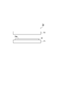
(光照射ユニット)
続いて、処理モジュール17の光照射ユニットU3について詳細に説明する。光照射ユニットU3は、図5に示すフラッド露光ユニット70を含む。フラッド露光ユニット70は、支持台71と光源72とを有する。
(Light irradiation unit)
Next, the light irradiation unit U3 of the
支持台71は、表面Waが上方に面した状態でウェハWを支持する。光源72は、支持台71により支持された表面Waに対し、上記励起光を照射する。上記励起光は、例えば200nmを超える波長を有する非電離放射線であり、250nmを超える波長を有する非電離放射線であってもよい。例えば光源72は、波長が365nmの紫外線を照射するUV−LEDを含んでいてもよい。
The
(コントローラ)
コントローラ100は、キャリアブロック4、処理ブロック5及びインタフェースブロック6を制御する。コントローラ100は、上記被膜をウェハWの表面Waに形成する被膜形成処理を実行するように処理モジュール14,15,16を制御することと、第一露光処理(露光装置3における露光処理)により発生した光増感剤から第二成分にエネルギーを供給して酸を発生させるように、光増感剤を励起するための光を被膜に照射する第二露光処理を実行するように処理モジュール17の光照射ユニットU3を制御することと、第二露光処理により発生した酸による触媒反応を促進するように被膜を加熱する第一加熱処理を実行するように処理モジュール17の熱処理ユニットU2を制御することと、第一現像液を被膜に供給する第一現像処理を実行するように処理モジュール17の液処理ユニットU1を制御することと、第一現像処理の後に、被膜内に残留した光増感剤から第二成分にエネルギーを供給して酸を発生させるように、光増感剤を励起するための光を被膜に照射する第三露光処理を実行するように処理モジュール17の光照射ユニットU3を制御することと、第三露光処理により発生した酸による触媒反応を促進するように被膜を加熱する第二加熱処理を実行するように処理モジュール17の熱処理ユニットU2を制御することと、第二現像液を被膜に供給する第二現像処理を実行するように処理モジュール17の液処理ユニットU1を制御することと、を実行するように構成されている。
(controller)
The
図6に例示するように、コントローラ100は、機能上のモジュール(以下、「機能モジュール」という。)として、搬送制御部111と、成膜制御部112と、フラッド露光制御部113と、PEB制御部114と、現像制御部115とを有する。
As illustrated in FIG. 6, the
搬送制御部111は、後述の基板処理手順に応じてウェハWを搬送するように、受け渡しアームA1,A8と、直接搬送アームA6と、昇降アームA7と、処理モジュール14,15,16,17の搬送アームA3とを制御する。成膜制御部112は、被膜形成処理を実行するように処理モジュール14,15,16の液処理ユニットU1及び熱処理ユニットU2を制御する。フラッド露光制御部113は、第二露光処理及び第三露光処理を実行するように処理モジュール17の光照射ユニットU3を制御する。PEB制御部114は、第一加熱処理及び第二加熱処理を実行するように処理モジュール17の熱処理ユニットU2を制御する。現像制御部115は、第一現像処理及び第二現像処理を実行するように処理モジュール17の液処理ユニットU1を制御する。
The
コントローラ100は、一つ又は複数の制御用コンピュータにより構成される。例えばコントローラ100は、図7に示す回路120を有する。回路120は、一つ又は複数のプロセッサ121と、メモリ122と、ストレージ123と、入出力ポート124と、タイマー125とを有する。
The
入出力ポート124は、受け渡しアームA1,A8と、搬送アームA3と、直接搬送アームA6と、昇降アームA7と、処理モジュール14,15,16の液処理ユニットU1及び熱処理ユニットU2と、処理モジュール17の液処理ユニットU1、熱処理ユニットU2及び光照射ユニットU3との間で電気信号の入出力を行う。タイマー125は、例えば一定周期の基準パルスをカウントすることで経過時間を計測する。
The input/
ストレージ123は、例えばハードディスク等、コンピュータによって読み取り可能な記録媒体を有する。記録媒体は、後述の基板処理手順をキャリアブロック4、処理ブロック5及びインタフェースブロック6に実行させるためのプログラムを記録している。記録媒体は、不揮発性の半導体メモリ、磁気ディスク及び光ディスク等の取り出し可能な媒体であってもよい。
The
メモリ122は、ストレージ123の記録媒体からロードしたプログラム及びプロセッサ121による演算結果を一時的に記録する。プロセッサ121は、メモリ122と協働して上記プログラムを実行することで、上述した各機能モジュールを構成する。なお、コントローラ100のハードウェア構成は、必ずしもプログラムにより各機能モジュールを構成するものに限られない。例えばコントローラ100の各機能モジュールは、専用の論理回路又はこれを集積したASIC(Application Specific Integrated Circuit)により構成されていてもよい。
The
〔基板処理方法〕
続いて、基板処理方法の一例として、コントローラ100の制御に応じて塗布・現像装置2が実行する基板処理手順を説明する。図8は、基板処理手順を示すフローチャートである。図9及び図10は、基板処理手順におけるウェハWの状態を示す模式図である。図9及び図10では、被膜Fのうち下層膜及び上層膜の図示を省略し、レジスト膜のみを図示している。
[Substrate processing method]
Next, as an example of the substrate processing method, a substrate processing procedure executed by the coating/developing
図8に示すように、基板処理手順は、ステップS01〜S09を順に含む。 As shown in FIG. 8, the substrate processing procedure includes steps S01 to S09 in order.
ステップS01では、コントローラ100による制御手順に従って、処理モジュール14,15,16が上記被膜形成処理を実行する。例えば、まず搬送制御部111が、キャリア11内のウェハWを棚ユニットU10に搬送するように受け渡しアームA1を制御し、このウェハWを処理モジュール14用のセルに配置するように昇降アームA7を制御し、このウェハWを処理モジュール14の各ユニットに搬送するように処理モジュール14の搬送アームA3を制御する。これに応じ、成膜制御部112は、ウェハWの表面Wa上に下層膜を形成するように処理モジュール14の液処理ユニットU1及び熱処理ユニットU2を制御する。
In step S01, the
その後、搬送制御部111は、下層膜が形成されたウェハWを棚ユニットU10に戻すように搬送アームA3を制御し、このウェハWを処理モジュール15用のセルに配置するように昇降アームA7を制御し、このウェハWを処理モジュール15の各ユニットに搬送するように処理モジュール15の搬送アームA3を制御する。これに応じ、成膜制御部112は、ウェハWの下層膜上にレジスト膜を形成するように処理モジュール15の液処理ユニットU1及び熱処理ユニットU2を制御する。
After that, the
その後、搬送制御部111は、ウェハWを棚ユニットU10に戻すように搬送アームA3を制御し、このウェハWを処理モジュール16用のセルに配置するように昇降アームA7を制御し、このウェハWを処理モジュール16の各ユニットに搬送するように処理モジュール16の搬送アームA3を制御する。これに応じ、成膜制御部112は、ウェハWのレジスト膜上に上層膜を形成するように処理モジュール16の液処理ユニットU1及び熱処理ユニットU2を制御する。
After that, the
その後、搬送制御部111は、ウェハWを棚ユニットU10に戻すように搬送アームA3を制御し、このウェハWを処理モジュール17用のセルに配置するように昇降アームA7を制御する。
After that, the
ステップS02では、コントローラ100による制御手順に従って、インタフェースブロック6がウェハWを露光装置3に送出する。具体的には、搬送制御部111が、棚ユニットU10のウェハWを棚ユニットU11に搬送するように直接搬送アームA6を制御し、このウェハWを露光装置3に送り出すように受け渡しアームA8を制御する。
In step S 02, the
ステップS03では、コントローラ100による制御手順に従って、インタフェースブロック6が、第一露光処理後のウェハWを露光装置3から受け入れる。具体的には、搬送制御部111が、第一露光処理後のウェハWを露光装置3から受け入れて棚ユニットU11に戻すように受け渡しアームA8を制御する。被膜Fのうち、第一露光処理が施された箇所には光増感剤Cが発生している(図9の(a)参照)。
In step S03, the
ステップS04では、コントローラ100による制御手順に従って、処理モジュール17が上記第二露光処理を実行する。具体的には、搬送制御部111が、棚ユニットU11のウェハWを光照射ユニットU3に搬送するように処理モジュール17の搬送アームA3を制御し、フラッド露光制御部113が、ウェハWの被膜Fに上記励起光を照射するように光照射ユニットU3を制御する。これにより、被膜Fの光増感剤Cが励起され、励起された光増感剤Cから上記第二成分にエネルギーが供給され、これに応じて第二成分が酸ACを発生させる(図9の(b)参照)。
In step S04, the
ステップS05では、コントローラ100による制御手順に従って、処理モジュール17が上記第一加熱処理を実行する。具体的には、搬送制御部111が、ウェハWを光照射ユニットU3から熱処理ユニットU2に搬送するように処理モジュール17の搬送アームA3を制御し、PEB制御部114が、被膜を第一温度にて加熱するように処理モジュール17の熱処理ユニットU2を制御する。第一温度は、例えば60〜200℃であり、70〜140℃であってもよい。第一加熱処理により、第二露光処理にて発生した酸による触媒反応が促進されるので、酸ACが存在していた箇所に、第一現像液に可溶な領域R1が形成される(図9の(c)参照)。
In step S05, the
ステップS06では、コントローラ100による制御手順に従って、処理モジュール17が上記第一現像処理を実行する。具体的には、搬送制御部111が、ウェハWを熱処理ユニットU2から液処理ユニットU1に搬送するように処理モジュール17の搬送アームA3を制御し、現像制御部115が、被膜Fに第一現像液を供給するように液処理ユニットU1を制御する。例えば現像制御部115は、ウェハWを回転させるように回転保持部30を制御し、ウェハWの回転中心の鉛直上方から被膜Fに第一現像液を供給するように現像液供給部40を制御する。これにより、被膜Fの領域R1(第一加熱処理における触媒反応が生じた箇所)が第一現像液に溶解する。
In step S06, the
その後、現像制御部115は、ウェハWの回転中心の鉛直上方から被膜Fにリンス液を供給するようにリンス液供給部60を制御する。これにより、被膜Fの領域R1が除去され、表面Wa上にレジストパターンP1(第一パターン)が形成される(図9の(d)参照)。
After that, the
ステップS07では、コントローラ100による制御手順に従って、処理モジュール17が上記第三露光処理を実行する。具体的には、搬送制御部111が、ウェハWを液処理ユニットU1から光照射ユニットU3に搬送するように処理モジュール17の搬送アームA3を制御し、フラッド露光制御部113が、ウェハWの被膜Fに上記励起光を照射するように光照射ユニットU3を制御する。これにより、被膜F内に残留した光増感剤Cが励起され、励起された光増感剤Cから上記第二成分にエネルギーが供給され、これに応じて第二成分が酸ACを発生させる(図10の(b)参照)。
In step S07, the
なお、被膜F内の光増感剤Cは、主としてレジストパターンP1の側部に残留している。このため、第三露光処理においては、レジストパターンP1の側部に集中して酸ACが発生する。 The photosensitizer C in the film F mainly remains on the side portion of the resist pattern P1. Therefore, in the third exposure process, the acid AC is concentrated on the side portion of the resist pattern P1.
ステップS08では、コントローラ100による制御手順に従って、処理モジュール17が上記第二加熱処理を実行する。具体的には、搬送制御部111が、ウェハWを光照射ユニットU3から熱処理ユニットU2に搬送するように処理モジュール17の搬送アームA3を制御し、PEB制御部114が、被膜を第二温度にて加熱するように処理モジュール17の熱処理ユニットU2を制御する。第二温度は、第一温度と同等であってもよく、第一温度より低くてもよい。第二加熱処理により、第三露光処理にて発生した酸による触媒反応が促進されるので、酸ACが集中している箇所(レジストパターンP1の側部)に、第二現像液に不溶な領域R2が形成される(図10の(c)参照)。
In step S08, the
ステップS09では、コントローラ100による制御手順に従って、処理モジュール17が上記第二現像処理を実行する。具体的には、搬送制御部111が、ウェハWを熱処理ユニットU2から液処理ユニットU1に搬送するように処理モジュール17の搬送アームA3を制御し、現像制御部115が、被膜Fに第二現像液を供給するように液処理ユニットU1を制御する。例えば現像制御部115は、ウェハWを回転させるように回転保持部30を制御し、ウェハWの回転中心の鉛直上方から被膜Fに第二現像液を供給するように現像液供給部50を制御する。これにより、被膜Fの領域R2以外の領域(第二加熱処理における触媒反応が生じていない箇所)が第二現像液に溶解する。
In step S09, the
その後、現像制御部115は、ウェハWの回転中心の鉛直上方から被膜Fにリンス液を供給するようにリンス液供給部60を制御する。これにより、被膜Fの領域R2以外の領域が除去され、レジストパターンP1を更に細分化したレジストパターンP2(第二パターン)が形成される(図10の(d)参照)。
After that, the
その後、搬送制御部111は、ウェハWを棚ユニットU10に戻すように処理モジュール17の搬送アームA3を制御し、このウェハWをキャリア11内に戻すように昇降アームA7及び受け渡しアームA1を制御する。以上で基板処理手順が完了する。
After that, the
〔本実施形態の効果〕
本実施形態に係る基板処理方法は、第一露光処理によって光増感剤Cを発生させる第一成分と、光増感剤Cからのエネルギーの供給に応じて酸ACを発生させる第二成分とを含む被膜FをウェハWの表面Waに形成する被膜形成処理と、第一露光処理にて発生した光増感剤Cから第二成分にエネルギーを供給して酸ACを発生させるように、光増感剤Cを励起するための光を被膜Fに照射する第二露光処理と、第二露光処理にて発生した酸ACによる触媒反応を促進するように被膜Fを加熱する第一加熱処理と、第一加熱処理における触媒反応が生じた箇所を溶解させる第一現像液を被膜Fに供給する第一現像処理と、第一現像処理の後に、被膜F内に残留した光増感剤Cから第二成分にエネルギーを供給して酸ACを発生させるように、光増感剤Cを励起するための光を被膜Fに照射する第三露光処理と、第三露光処理にて発生した酸ACによる触媒反応を促進するように被膜Fを加熱する第二加熱処理と、第二加熱処理における触媒反応が生じていない箇所を溶解させる第二現像液を被膜Fに供給する第二現像処理と、を含む。
[Effects of this embodiment]
The substrate processing method according to the present embodiment includes a first component that generates a photosensitizer C by a first exposure process, and a second component that generates an acid AC in response to the supply of energy from the photosensitizer C. A film forming process for forming a film F containing W on the surface Wa of the wafer W and a photosensitizer C generated in the first exposure process to supply energy to the second component to generate an acid AC. A second exposure treatment of irradiating the coating F with light for exciting the sensitizer C, and a first heat treatment of heating the coating F so as to promote the catalytic reaction by the acid AC generated in the second exposure treatment. From the photosensitizer C remaining in the coating F after the first developing treatment in which a first developing solution that dissolves the portion where the catalytic reaction has occurred in the first heat treatment is supplied to the coating F; A third exposure treatment of irradiating the coating F with light for exciting the photosensitizer C so that the acid AC is generated by supplying energy to the second component, and the acid AC generated in the third exposure treatment. A second heat treatment for heating the coating F so as to accelerate the catalytic reaction by the second heat treatment, and a second developing treatment for supplying the coating F with a second developing solution that dissolves a portion of the second heat treatment in which no catalytic reaction occurs. including.
この基板処理方法によれば、酸触媒反応が生じた箇所を溶解させる第一現像処理を行うことで得られたレジストパターンP1に対し、酸触媒反応が生じていない箇所を溶解させる第二現像処理を更に行うことで、レジストパターンP1を更に細分化したレジストパターンP2が得られる。 According to this substrate processing method, with respect to the resist pattern P1 obtained by performing the first development treatment for dissolving the portion where the acid catalyst reaction has occurred, the second development treatment for dissolving the portion where the acid catalyst reaction has not occurred By further performing the above step, a resist pattern P2 obtained by further subdividing the resist pattern P1 can be obtained.
第一現像処理は、第二露光処理及び第一加熱処理の後に行われる。第二露光処理では、第一露光処理において露光された領域(以下、「第一領域」という。)の光増感剤Cが励起され、励起された光増感剤Cから第二成分にエネルギーが供給されることで、第一領域の酸ACが増殖する。第一加熱処理では、酸触媒反応が加熱によって促進される。第二露光処理により第一領域の酸ACが増殖しているので、第一加熱処理においては酸触媒反応が効率よく進行する。このため、被膜Fの過剰な加熱による溶解を抑制しつつ、酸触媒反応を促進することができる。酸触媒反応の促進により、第一領域とその他の領域とで、第一現像液に対する溶解性の差異が顕著になるので、レジストパターンP1を高い信頼性で形成できる。 The first development process is performed after the second exposure process and the first heating process. In the second exposure process, the photosensitizer C in the region exposed in the first exposure process (hereinafter, referred to as “first region”) is excited, and the excited photosensitizer C is energized to the second component. Is supplied, the acid AC in the first region grows. In the first heat treatment, the acid-catalyzed reaction is accelerated by heating. Since the acid AC in the first region is proliferated by the second exposure treatment, the acid catalytic reaction efficiently proceeds in the first heat treatment. Therefore, the acid-catalyzed reaction can be promoted while suppressing the dissolution of the coating film F due to excessive heating. By promoting the acid-catalyzed reaction, the difference in solubility in the first developing solution between the first region and the other regions becomes remarkable, so that the resist pattern P1 can be formed with high reliability.
第二現像処理は、第三露光処理及び第二加熱処理の後に行われる。第三露光処理では、レジストパターンP1のうち光増感剤Cが残留している領域(以下、「第二領域」という。)の酸が増殖する。第二加熱処理では、酸触媒反応が加熱によって促進される。第三露光処理により第二領域の酸が増殖しているので、第二加熱処理においても酸触媒反応が効率よく進行する。このため、被膜Fの過剰な加熱による溶解を抑制しつつ、酸触媒反応を促進することができる。酸触媒反応の促進により、第二領域とその他の領域とで、第二現像液に対する溶解性の差異が顕著になるので、レジストパターンP2も高い信頼性で形成できる。従って、フォトリソグラフィーによるレジストパターンの微細化に有効である。 The second development process is performed after the third exposure process and the second heating process. In the third exposure process, the acid in the region of the resist pattern P1 where the photosensitizer C remains (hereinafter, referred to as “second region”) grows. In the second heat treatment, the acid-catalyzed reaction is accelerated by heating. Since the acid in the second region is proliferated by the third exposure treatment, the acid-catalyzed reaction efficiently proceeds even in the second heat treatment. Therefore, the acid-catalyzed reaction can be promoted while suppressing the dissolution of the coating film F due to excessive heating. By promoting the acid-catalyzed reaction, the difference in solubility in the second developer between the second region and the other regions becomes noticeable, so that the resist pattern P2 can be formed with high reliability. Therefore, it is effective for miniaturizing the resist pattern by photolithography.
第二加熱処理では、第一加熱処理に比較して低い温度にて被膜Fを加熱してもよい。この場合、第二加熱処理における被膜Fの過剰な加熱が更に抑制されるので、レジストパターンP2を更に高い信頼性で形成できる。 In the second heat treatment, the coating F may be heated at a lower temperature than the first heat treatment. In this case, since excessive heating of the coating film F in the second heat treatment is further suppressed, the resist pattern P2 can be formed with higher reliability.
以上、実施形態について説明したが、本発明は必ずしも上述した実施形態に限定されるものではなく、その要旨を逸脱しない範囲で様々な変更が可能である。処理対象の基板は半導体ウェハに限られず、例えばガラス基板、マスク基板、FPD(Flat Panel Display)等であってもよい。 Although the embodiments have been described above, the present invention is not necessarily limited to the above-described embodiments, and various modifications can be made without departing from the scope of the invention. The substrate to be processed is not limited to the semiconductor wafer, and may be, for example, a glass substrate, a mask substrate, an FPD (Flat Panel Display), or the like.
W…ウェハ(基板)、Wa…表面、2…塗布・現像装置(基板処理装置)、14,15,16…処理モジュール(被膜形成部)、U2…熱処理ユニット(加熱部)、U3…光照射ユニット(光照射部)、40…現像液供給部(第一現像液供給部)、50…現像液供給部(第二現像液供給部)、F…被膜、C…光増感剤、AC…酸。 W... Wafer (substrate), Wa... Surface, 2... Coating/developing device (substrate processing device), 14, 15, 16... Processing module (coating forming part), U2... Heat treatment unit (heating part), U3... Light irradiation Unit (light irradiation unit), 40... Developer solution supply unit (first developer solution supply unit), 50... Developer solution supply unit (second developer solution supply unit), F... Coating film, C... Photosensitizer, AC... acid.
Claims (6)
前記第一露光処理にて発生した前記光増感剤から前記第二成分に前記エネルギーを供給して酸を発生させるように、前記光増感剤を励起するための光を前記被膜に照射する第二露光処理と、
前記第二露光処理にて発生した酸による触媒反応を促進するように前記被膜を加熱する第一加熱処理と、
前記第一加熱処理における前記触媒反応が生じた箇所を溶解させる第一現像液を前記被膜に供給する第一現像処理と、
前記第一現像処理の後に、前記被膜内に残留した前記光増感剤から前記第二成分に前記エネルギーを供給して酸を発生させるように、前記光増感剤を励起するための光を前記被膜に照射する第三露光処理と、
前記第三露光処理にて発生した酸による前記触媒反応を促進するように前記被膜を加熱する第二加熱処理と、
前記第二加熱処理における前記触媒反応が生じていない箇所を溶解させる第二現像液を前記被膜に供給する第二現像処理と、を含む基板処理方法。 Forming a coating film on the surface of a substrate that includes a first component that generates a photosensitizer by a first exposure treatment and a second component that generates an acid in response to the supply of energy from the photosensitizer. Processing and
The film is irradiated with light for exciting the photosensitizer so that the photosensitizer generated in the first exposure process supplies the energy to the second component to generate an acid. A second exposure process,
A first heat treatment for heating the coating so as to promote a catalytic reaction by the acid generated in the second exposure treatment,
A first developing treatment for supplying to the coating a first developing solution that dissolves the portion where the catalytic reaction occurs in the first heat treatment,
After the first development treatment, light for exciting the photosensitizer is supplied from the photosensitizer remaining in the coating film so as to supply the energy to the second component to generate an acid. A third exposure treatment for irradiating the coating,
A second heat treatment for heating the coating so as to promote the catalytic reaction due to the acid generated in the third exposure treatment,
A second substrate processing method, comprising: a second developing process of supplying a second developing solution that dissolves a portion of the second heat treatment where the catalytic reaction has not occurred, to the coating.
前記被膜を前記基板の表面に形成する被膜形成部と、
前記光増感剤を励起するための光を前記被膜に照射する光照射部と、
前記被膜を加熱する加熱部と、
前記被膜に前記第一現像液を供給する第一現像液供給部と、
前記被膜に前記第二現像液を供給する第二現像液供給部と、を備える基板処理装置。 An apparatus for performing the substrate processing method according to claim 1.
A coating film forming portion for forming the coating film on the surface of the substrate,
A light irradiation unit for irradiating the coating with light for exciting the photosensitizer,
A heating unit for heating the coating,
A first developer supply unit for supplying the first developer to the film,
A substrate processing apparatus comprising: a second developing solution supply unit that supplies the second developing solution to the coating film.
Priority Applications (2)
| Application Number | Priority Date | Filing Date | Title |
|---|---|---|---|
| JP2016152862A JP6726558B2 (en) | 2016-08-03 | 2016-08-03 | Substrate processing method, substrate processing apparatus, and recording medium |
| KR1020170098548A KR102305412B1 (en) | 2016-08-03 | 2017-08-03 | Substrate processing method, substrate processing apparatus and recording medium |
Applications Claiming Priority (1)
| Application Number | Priority Date | Filing Date | Title |
|---|---|---|---|
| JP2016152862A JP6726558B2 (en) | 2016-08-03 | 2016-08-03 | Substrate processing method, substrate processing apparatus, and recording medium |
Publications (2)
| Publication Number | Publication Date |
|---|---|
| JP2018022032A JP2018022032A (en) | 2018-02-08 |
| JP6726558B2 true JP6726558B2 (en) | 2020-07-22 |
Family
ID=61166142
Family Applications (1)
| Application Number | Title | Priority Date | Filing Date |
|---|---|---|---|
| JP2016152862A Active JP6726558B2 (en) | 2016-08-03 | 2016-08-03 | Substrate processing method, substrate processing apparatus, and recording medium |
Country Status (2)
| Country | Link |
|---|---|
| JP (1) | JP6726558B2 (en) |
| KR (1) | KR102305412B1 (en) |
Families Citing this family (1)
| Publication number | Priority date | Publication date | Assignee | Title |
|---|---|---|---|---|
| WO2022255119A1 (en) * | 2021-06-01 | 2022-12-08 | 東京エレクトロン株式会社 | Photoresist composition, method for forming resist pattern, method for manufacturing semiconductor device, and substrate processing device |
Family Cites Families (8)
| Publication number | Priority date | Publication date | Assignee | Title |
|---|---|---|---|---|
| US5925410A (en) * | 1997-05-06 | 1999-07-20 | Micron Technology, Inc. | Vibration-enhanced spin-on film techniques for semiconductor device processing |
| JP3943741B2 (en) * | 1999-01-07 | 2007-07-11 | 株式会社東芝 | Pattern formation method |
| JP3800416B2 (en) * | 2001-10-18 | 2006-07-26 | 東京エレクトロン株式会社 | Coating processing method and coating processing apparatus |
| JP2005159295A (en) * | 2003-09-18 | 2005-06-16 | Nec Kagoshima Ltd | Substrate processing apparatus and processing method |
| JP4554665B2 (en) * | 2006-12-25 | 2010-09-29 | 富士フイルム株式会社 | PATTERN FORMATION METHOD, POSITIVE RESIST COMPOSITION FOR MULTIPLE DEVELOPMENT USED FOR THE PATTERN FORMATION METHOD, NEGATIVE DEVELOPMENT SOLUTION USED FOR THE PATTERN FORMATION METHOD, AND NEGATIVE DEVELOPMENT RINSE SOLUTION USED FOR THE PATTERN FORMATION METHOD |
| JP5988115B2 (en) * | 2013-02-20 | 2016-09-07 | 国立大学法人大阪大学 | Resist pattern forming method |
| US9519227B2 (en) * | 2014-02-24 | 2016-12-13 | Tokyo Electron Limited | Metrology for measurement of photosensitizer concentration within photo-sensitized chemically-amplified resist (PS-CAR) |
| JP6175455B2 (en) | 2015-01-22 | 2017-08-02 | 東京エレクトロン株式会社 | Resist pattern forming method |
-
2016
- 2016-08-03 JP JP2016152862A patent/JP6726558B2/en active Active
-
2017
- 2017-08-03 KR KR1020170098548A patent/KR102305412B1/en active Active
Also Published As
| Publication number | Publication date |
|---|---|
| JP2018022032A (en) | 2018-02-08 |
| KR102305412B1 (en) | 2021-09-27 |
| KR20180015595A (en) | 2018-02-13 |
Similar Documents
| Publication | Publication Date | Title |
|---|---|---|
| JP6585242B2 (en) | Substrate cleaning apparatus, substrate cleaning method, and storage medium | |
| US9454081B2 (en) | Line pattern collapse mitigation through gap-fill material application | |
| JP7085621B2 (en) | Substrate processing methods, substrate processing equipment, and computer-readable recording media | |
| JP7535933B2 (en) | Development method and substrate processing system | |
| TWI647740B (en) | Substrate processing method, substrate processing apparatus, and recording medium | |
| JP2014099583A (en) | Substrate cleaning device, substrate cleaning systems, substrate cleaning method, and storage medium | |
| JP6704258B2 (en) | Substrate processing method, substrate processing apparatus, and computer-readable recording medium | |
| JP6148210B2 (en) | Development method and computer-readable recording medium | |
| JP7507297B2 (en) | Liquid processing apparatus, liquid processing method, and computer-readable recording medium | |
| JP7738125B2 (en) | Development processing method, storage medium, and development processing device | |
| KR20190040898A (en) | Development processing apparatus, development processing method, and storage medium | |
| JP6215787B2 (en) | Development method, development apparatus, and computer-readable recording medium | |
| JP6726558B2 (en) | Substrate processing method, substrate processing apparatus, and recording medium | |
| JP6175455B2 (en) | Resist pattern forming method | |
| JP7556968B2 (en) | SUBSTRATE PROCESSING METHOD AND SUBSTRATE PROCESSING APPARATUS | |
| KR102917237B1 (en) | Substrate processing method, recording medium and substrate processing apparatus | |
| JP6145065B2 (en) | Substrate processing method, substrate processing apparatus, and recording medium | |
| JP6626734B2 (en) | Substrate processing apparatus, substrate processing method, and computer-readable recording medium | |
| WO2024241937A1 (en) | Development method and substrate processing system | |
| KR20250037538A (en) | Substrate processing device, substrate processing method, and substrate processing program | |
| JPH0750678B2 (en) | Wafer edge exposure method |
Legal Events
| Date | Code | Title | Description |
|---|---|---|---|
| A621 | Written request for application examination |
Free format text: JAPANESE INTERMEDIATE CODE: A621 Effective date: 20190611 |
|
| A977 | Report on retrieval |
Free format text: JAPANESE INTERMEDIATE CODE: A971007 Effective date: 20200305 |
|
| TRDD | Decision of grant or rejection written | ||
| A01 | Written decision to grant a patent or to grant a registration (utility model) |
Free format text: JAPANESE INTERMEDIATE CODE: A01 Effective date: 20200602 |
|
| A61 | First payment of annual fees (during grant procedure) |
Free format text: JAPANESE INTERMEDIATE CODE: A61 Effective date: 20200629 |
|
| R150 | Certificate of patent or registration of utility model |
Ref document number: 6726558 Country of ref document: JP Free format text: JAPANESE INTERMEDIATE CODE: R150 |
|
| R250 | Receipt of annual fees |
Free format text: JAPANESE INTERMEDIATE CODE: R250 |
|
| R250 | Receipt of annual fees |
Free format text: JAPANESE INTERMEDIATE CODE: R250 |
|
| R250 | Receipt of annual fees |
Free format text: JAPANESE INTERMEDIATE CODE: R250 |