JP6707835B2 - Anisotropic conductive film - Google Patents
Anisotropic conductive film Download PDFInfo
- Publication number
- JP6707835B2 JP6707835B2 JP2015211452A JP2015211452A JP6707835B2 JP 6707835 B2 JP6707835 B2 JP 6707835B2 JP 2015211452 A JP2015211452 A JP 2015211452A JP 2015211452 A JP2015211452 A JP 2015211452A JP 6707835 B2 JP6707835 B2 JP 6707835B2
- Authority
- JP
- Japan
- Prior art keywords
- conductive particles
- anisotropic conductive
- conductive film
- insulating adhesive
- less
- Prior art date
- Legal status (The legal status is an assumption and is not a legal conclusion. Google has not performed a legal analysis and makes no representation as to the accuracy of the status listed.)
- Active
Links
Images


Description
本発明は、異方性導電フィルムに関する。 The present invention relates to an anisotropic conductive film.
絶縁性樹脂バインダに導電粒子を分散させた異方性導電フィルムが、ICチップ等の電子部品を配線基板等に実装する際に広く使用されているが、このような異方性導電フィルムにおいては、導電粒子同士が連結もしくは凝集した状態で存在していることが知られている。このため、異方性導電フィルムを、電子機器の軽量小型化に伴い狭ピッチ化しているICチップの端子と配線基板の端子との接続に適用した場合、異方性導電フィルム中に連結もしくは凝集した状態で存在している導電粒子により、隣接する端子間で短絡が生ずる場合があった。 Anisotropic conductive films in which conductive particles are dispersed in an insulating resin binder are widely used when mounting electronic components such as IC chips on wiring boards and the like. In such anisotropic conductive films, It is known that conductive particles exist in a state of being connected or aggregated. Therefore, when the anisotropic conductive film is applied to the connection between the terminals of the IC chip and the terminals of the wiring board whose pitch is narrowed as the weight and size of electronic devices are reduced, the anisotropic conductive film is connected or aggregated in the anisotropic conductive film. Due to the conductive particles existing in this state, a short circuit may occur between adjacent terminals.
従来、このような狭ピッチ化に対応した異方性導電フィルムとして、フィルム中に導電粒子を規則配列させたものが提案されている。例えば、延伸可能なフィルムに粘着層を形成し、その粘着層表面に導電粒子を単層で密集充填した後、このフィルムを導電粒子間距離が所期の距離になるまで2軸延伸処理して導電粒子を規則配列させ、その後、導電粒子に対し異方性導電フィルムの構成要素となる絶縁性接着ベース層を押し当て、導電粒子を絶縁性接着ベース層に転写させて得た異方性導電フィルムが提案されている(特許文献1)。また、凹部を表面に有する転写型の凹部形成面に導電粒子を散布し、凹部形成面をスキージして凹部に導電粒子を保持させ、その上から転写用の粘着層が形成された粘着フィルムを押し当て、粘着層に導電粒子を一次転写させ、次に、粘着層に付着した導電粒子に対し、異方性導電フィルムの構成要素となる絶縁性接着ベース層を押し当て、導電粒子を絶縁性接着ベース層に転写させて得た異方性導電フィルムも提案されている(特許文献2)。これらの異方性導電フィルムについては、一般に、導電粒子側表面に、導電粒子を覆うように絶縁性接着カバー層が積層されている。 Heretofore, as an anisotropic conductive film corresponding to such a narrow pitch, a film in which conductive particles are regularly arranged is proposed. For example, an adhesive layer is formed on a stretchable film, the surface of the adhesive layer is densely packed with a single layer of conductive particles, and the film is biaxially stretched until the distance between the conductive particles reaches a desired distance. Anisotropic conductivity obtained by arranging conductive particles in a regular arrangement and then pressing the insulating adhesive base layer that is a component of the anisotropic conductive film against the conductive particles to transfer the conductive particles to the insulating adhesive base layer. A film has been proposed (Patent Document 1). In addition, conductive particles are dispersed on the transfer-type recess forming surface having a recess on the surface, the recess forming surface is squeegeeed to hold the conductive particles in the recess, and an adhesive film having a transfer adhesive layer formed thereon is formed. The conductive particles are first transferred to the adhesive layer by pressing, and then the insulating adhesive base layer, which is a component of the anisotropic conductive film, is pressed against the conductive particles attached to the adhesive layer to insulate the conductive particles. An anisotropic conductive film obtained by transferring to an adhesive base layer has also been proposed (Patent Document 2). In these anisotropic conductive films, an insulating adhesive cover layer is generally laminated on the surface of the conductive particles so as to cover the conductive particles.
しかしながら、導電粒子は静電気等により凝集して二次粒子化し易いため、導電粒子を一次粒子として常時単独で存在させることは困難である。このため、特許文献1や特許文献2の技術には以下のような問題が生ずる。即ち、特許文献1の場合には、延伸可能フィルムの全面に導電粒子を欠陥なく単層で密集充填することが難しく、導電粒子が凝集状態で延伸可能フィルムに充填され、ショートの原因となったり、充填されない領域(いわゆる「抜け」)が生じ、導通不良の原因になったりするという問題があった。また、特許文献2の場合、転写型の凹部が粒子径の大きな導電粒子で覆われると、その後のスキージにより取り除かれて、導電粒子を保持していない凹部が生じ、異方性導電フィルムに導電粒子の「抜け」が生じて導通不良の原因になったり、反対に凹部に多数の小さな導電粒子が押し込まれると、絶縁性接着ベース層に転写させた際、導電粒子の凝集が生じたり、また、凹部の底部側に位置している導電粒子が、絶縁性接着ベース層と接触していないため、絶縁性接着ベース層の表面に散らばり、規則配列が損なわれ、ショートや導通不良の原因になったりするという問題があった。 However, it is difficult for the conductive particles to always exist alone as the primary particles because the conductive particles easily aggregate due to static electricity or the like to form secondary particles. Therefore, the following problems occur in the techniques of Patent Document 1 and Patent Document 2. That is, in the case of Patent Document 1, it is difficult to densely fill the entire surface of the stretchable film with conductive particles in a single layer without defects, and the conductive particles are packed in the stretchable film in an aggregated state, which may cause a short circuit. However, there is a problem in that an unfilled region (so-called “removal”) occurs, which may cause conduction failure. Further, in the case of Patent Document 2, when the transfer-type recess is covered with the conductive particles having a large particle diameter, the transfer-type recess is removed by a squeegee thereafter to form a recess that does not hold the conductive particles, and the anisotropic conductive film is electrically conductive. If particles “drop out” occur and cause conduction failure, or conversely, a large number of small conductive particles are pressed into the recesses, when transferred to the insulating adhesive base layer, the conductive particles aggregate, or Since the conductive particles located on the bottom side of the recess are not in contact with the insulating adhesive base layer, the conductive particles are scattered on the surface of the insulating adhesive base layer, which damages the regular arrangement and causes a short circuit or poor conduction. There was a problem that
このように、特許文献1や2では、異方性導電フィルムに規則的パターンで配列されるべき導電粒子の「抜け」と「凝集」とをどのように制御すべきか、ということについては、十分に考慮されていないというのが実情である。 As described above, in Patent Documents 1 and 2, it is sufficient to know how to control “dropout” and “aggregation” of conductive particles to be arranged in a regular pattern on the anisotropic conductive film. The fact is that it is not taken into consideration.
本発明の目的は、以上の従来の技術の問題点を解決することであり、規則的パターンで配列されるべき導電粒子の「抜け」と「凝集」の観点から、ショートや導通不良の発生が大きく抑制された異方性導電フィルムを提供することである。 An object of the present invention is to solve the above-mentioned problems of the conventional techniques, and from the viewpoint of “missing” and “aggregation” of conductive particles to be arranged in a regular pattern, occurrence of a short circuit or poor conduction occurs. An object of the present invention is to provide a significantly suppressed anisotropic conductive film.
本発明者は、平面格子の格子点に導電粒子を配置する際に、異方性導電フィルムの基準領域に想定される平面格子パターンの全格子点に対する、「導電粒子が配置されていない格子点の割合」と「導電粒子が凝集して配置されている格子点の割合」とを制御することにより、上述の目的を達成できることを見出し、本発明を完成させるに至った。また、そのような異方性導電フィルムが、転写体の凹部に導電粒子を配置するのではなく、表面に柱状の凸部が形成された転写体の当該凸部の先端に導電粒子を付着させて転写を行うことにより製造できることを見出し、本発明の製造方法を完成させた。 The present inventor, when arranging the conductive particles at the lattice points of the plane lattice, with respect to all the lattice points of the plane lattice pattern assumed in the reference region of the anisotropic conductive film, "the lattice points where the conductive particles are not arranged" The inventors have found that the above-mentioned object can be achieved by controlling the "ratio of" and the "ratio of lattice points where conductive particles are aggregated and arranged", and have completed the present invention. In addition, such an anisotropic conductive film does not arrange the conductive particles in the concave portions of the transfer body, but attaches the conductive particles to the tips of the convex portions of the transfer body having the columnar convex portions formed on the surface. It was found that it can be produced by transferring by transfer, and completed the production method of the present invention.
即ち、本発明は、絶縁性接着ベース層に導電粒子が平面格子パターンの格子点に配置された構造の異方性導電フィルムであって、
異方性導電フィルムの基準領域に想定される平面格子パターンの全格子点に対する導電粒子が配置されていない格子点の割合が、20%未満であり、
該平面格子パターンの全格子点に対する複数の導電粒子が凝集して配置されている格子点の割合が、15%以下であり、抜けと凝集の合計が25%未満である異方性導電フィルムを提供する。
That is, the present invention is an anisotropic conductive film having a structure in which conductive particles in the insulating adhesive base layer are arranged at lattice points of a plane lattice pattern,
The ratio of the lattice points in which the conductive particles are not arranged to all the lattice points of the plane lattice pattern assumed in the reference region of the anisotropic conductive film is less than 20%,
An anisotropic conductive film having a ratio of lattice points in which a plurality of conductive particles are aggregated and arranged with respect to all lattice points of the plane lattice pattern is 15% or less, and a total of voids and aggregation is less than 25%. provide.
また、本発明は、絶縁性接着ベース層と絶縁性接着カバー層とが積層され、それらの界面近傍に導電粒子が平面格子パターンの格子点に配置された構造の異方性導電フィルムであって、
異方性導電フィルムの基準領域に想定される平面格子パターンの全格子点に対する導電粒子が配置されていない格子点の割合が、20%未満であり、
該平面格子パターンの全格子点に対する複数の導電粒子が凝集して配置されている格子点の割合が、5%以下である異方性導電フィルムを提供する。この場合も、抜けと凝集の合計は好ましくは25%未満である。
Further, the present invention is an anisotropic conductive film having a structure in which an insulating adhesive base layer and an insulating adhesive cover layer are laminated, and conductive particles are arranged in the vicinity of the interface between them at lattice points of a plane lattice pattern. ,
The ratio of the lattice points in which the conductive particles are not arranged to all the lattice points of the plane lattice pattern assumed in the reference region of the anisotropic conductive film is less than 20%,
Provided is an anisotropic conductive film in which the ratio of lattice points in which a plurality of conductive particles are aggregated and arranged with respect to all lattice points of the plane lattice pattern is 5% or less. Also in this case, the total of omission and aggregation is preferably less than 25%.
また、本発明は、絶縁性接着ベース層と絶縁性接着カバー層とが積層され、それらの界面近傍に導電粒子が平面格子パターンの格子点に配置された構造の異方性導電フィルムの製造方法であって、以下の工程(イ)〜(ホ):
<工程(イ)>
平面格子パターンの格子点に相当する柱状の凸部が表面に形成された転写体を用意する工程;
<工程(ロ)>
該転写体の凸部の少なくとも天面を微粘着層とする工程;
<工程(ハ)>
該転写体の凸部の微粘着層に導電粒子を付着させる工程;
<工程(ニ)>
該転写体の導電粒子が付着した側の表面に絶縁性接着ベース層を重ねて押圧することにより、絶縁性接着ベース層に導電粒子を転着させる工程;及び
<工程(ホ)>
導電粒子が転着した絶縁性接着ベース層に対し、導電粒子転着面側から絶縁性接着カバー層を積層する工程
を有する製造方法を提供する。
The present invention also provides a method for producing an anisotropic conductive film having a structure in which an insulating adhesive base layer and an insulating adhesive cover layer are laminated, and conductive particles are arranged in the vicinity of the interface between them at lattice points of a plane lattice pattern. The following steps (a) to (e):
<Process (a)>
A step of preparing a transfer body having columnar convex portions corresponding to lattice points of a plane lattice pattern formed on the surface;
<Process (b)>
A step of forming at least the top surface of the convex portion of the transfer member as a slight adhesive layer;
<Process (C)>
A step of attaching conductive particles to the slightly adhesive layer on the convex portion of the transfer member;
<Process (d)>
A step of transferring the conductive particles to the insulating adhesive base layer by stacking and pressing the insulating adhesive base layer on the surface of the transfer body on which the conductive particles adhere; and <step (e)>
Provided is a manufacturing method including a step of laminating an insulating adhesive cover layer from the conductive particle transfer surface side to an insulating adhesive base layer onto which conductive particles are transferred.
更に、本発明は、第1の電子部品の端子と、第2の電子部品の端子とが、本発明の異方性導電フィルムにより異方性導電接続された接続構造体を提供する。 Furthermore, the present invention provides a connection structure in which the terminals of the first electronic component and the terminals of the second electronic component are anisotropically conductively connected by the anisotropic conductive film of the present invention.
本発明の異方性導電フィルムにおいては、基準領域に想定される平面格子パターンの全格子点に対する「導電粒子が配置されていない格子点」の割合が20%未満に設定され、「複数の導電粒子が凝集して配置されている格子点」の割合が15%以下に設定され、しかも抜けと凝集の合計が25%未満に設定されている。このため、本発明の異方性導電フィルムを異方性導電接続に適用した場合、良好な初期導通抵抗値とエージング後の良好な導通信頼性とを実現でき、ショートの発生も抑制できる。また、COGのみならず、バンプ面積や距離が十分に大きい電子部品、例えばFOG等に対して、経済性に優れる。 In the anisotropic conductive film of the present invention, the ratio of "lattice points where conductive particles are not arranged" to all the lattice points of the plane lattice pattern assumed in the reference region is set to less than 20%, and "plurality of conductive layers" is set. The ratio of "lattice points where particles are aggregated and arranged" is set to 15% or less, and the total of voids and aggregation is set to less than 25%. Therefore, when the anisotropic conductive film of the present invention is applied to anisotropic conductive connection, a good initial conduction resistance value and a good conduction reliability after aging can be realized, and a short circuit can be suppressed. Further, not only COG but also an electronic component having a sufficiently large bump area and distance, such as FOG, is excellent in economic efficiency.
本発明の好ましい異方性導電フィルムにおいては、基準領域に想定される平面格子パターンの全格子点に対する「導電粒子が配置されていない格子点」の割合が20%未満に設定され、しかも「複数の導電粒子が凝集して配置されている格子点」の割合が5%以下である。このため、本発明の異方性導電フィルムを異方性導電接続に適用した場合、良好な初期導通抵抗値とエージング後の良好な導通信頼性とを実現でき、ショートの発生も抑制できる。 In the preferred anisotropic conductive film of the present invention, the ratio of “lattice points where conductive particles are not arranged” to all the lattice points of the plane lattice pattern assumed in the reference region is set to less than 20%, The ratio of “lattice points where the conductive particles are aggregated and arranged” is 5% or less. Therefore, when the anisotropic conductive film of the present invention is applied to anisotropic conductive connection, a good initial conduction resistance value and a good conduction reliability after aging can be realized, and a short circuit can be suppressed.
また、本発明の異方性導電フィルムの製造方法においては、平面格子パターンの格子点に相当する柱状の凸部が表面に形成された転写体を使用し、その凸部の天面に形成した微粘着層に導電粒子を付着させた後に、その導電粒子を絶縁性接着ベース層に転写する。このため、異方性導電フィルムの基準領域に想定される平面格子パターンの全格子点に対する「導電粒子が配置されていない格子点」の割合を20%未満とし且つ平面格子パターンの全格子点に対する「複数の導電粒子が凝集して配置されている格子点」の割合を5%以下にすることができる。よって、本発明の製造方法は、経済的に有利に異方性導電フィルムを製造することができ、この異方性導電フィルムを用いれば、狭ピッチ化したICチップと配線基板とを、ショートや導通不良の発生を大きく抑制しつつ、異方性導電接続が可能となる。 Further, in the method for producing an anisotropic conductive film of the present invention, a transfer body having columnar convex portions corresponding to the lattice points of the plane lattice pattern formed on the surface is used, and formed on the top surface of the convex portions. After attaching the conductive particles to the slightly adhesive layer, the conductive particles are transferred to the insulating adhesive base layer. Therefore, the ratio of “lattice points where conductive particles are not arranged” to all the lattice points of the plane lattice pattern assumed in the reference area of the anisotropic conductive film is set to less than 20% and all the lattice points of the plane lattice pattern are set. The ratio of “lattice points where a plurality of conductive particles are aggregated and arranged” can be set to 5% or less. Therefore, the production method of the present invention can economically produce an anisotropic conductive film, and by using this anisotropic conductive film, the IC chip and the wiring board having a narrow pitch can be short-circuited or short-circuited. Anisotropic conductive connection is possible while greatly suppressing the occurrence of conduction failure.
本発明の異方性導電フィルムは、絶縁性接着ベース層と絶縁性接着カバー層とが積層され、それらの界面近傍に導電粒子が平面格子パターンの格子点に配置された構造を有する。この異方性導電フィルムの基準領域に想定される平面格子パターンの全格子点に対する導電粒子が配置されていない格子点の割合は、20%未満であり、該平面格子パターンの全格子点に対する複数の導電粒子が凝集して配置されている格子点の割合は、15%以下であり、抜けと凝集の合計が25%未満である。以下、本発明の異方性導電フィルムを図面を参照しながら詳細に説明する。 The anisotropic conductive film of the present invention has a structure in which an insulating adhesive base layer and an insulating adhesive cover layer are laminated, and conductive particles are arranged in the vicinity of their interface at lattice points of a plane lattice pattern. The ratio of the lattice points in which the conductive particles are not arranged to all the lattice points of the plane lattice pattern assumed in the reference region of this anisotropic conductive film is less than 20%, and the plurality of lattice points to all the lattice points of the plane lattice pattern are plural. The ratio of the lattice points in which the conductive particles are arranged in agglomeration is 15% or less, and the total of voids and agglomeration is less than 25%. Hereinafter, the anisotropic conductive film of the present invention will be described in detail with reference to the drawings.
<異方性導電フィルム>
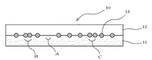
図1(断面図)と図2(平面透視図)に示すように、本発明の異方性導電フィルム10は、絶縁性接着ベース層11と絶縁性接着カバー層12とが積層され、それらの界面近傍に導電粒子13が平面格子パターン(図2の点線)の格子点に配置された構造を有する。図1及び図2では、平面格子パターンは、異方性導電フィルム10の長手方向とそれに直交する方向(短手方向)に沿って想定されているが、長手方向と短手方向とに対し全体が傾斜して想定されてもよい。ここで、矢印Aは、平面格子の格子点に導電粒子が配置されていない位置、いわゆる導電粒子が「抜け」ている位置を示している。なお、矢印Bは、導電粒子同士が接触して凝集している位置を示しており、矢印Cは、導電粒子同士が非接触で凝集している位置を示している。ここで、「非接触で凝集」するとは、導電粒子同士が導電粒子の平均粒子径の25%を超えない範囲で近接していることを意味する。
<Anisotropic conductive film>
As shown in FIG. 1 (cross-sectional view) and FIG. 2 (planar perspective view), an anisotropic
(導電粒子の「抜け」)
本発明の異方性導電フィルムにおいては、異方性導電フィルムの基準領域に想定される平面格子パターンの全格子点に対する「導電粒子が配置されていない格子点」(図2のA)の割合(導電粒子が抜けている格子の割合)を20%未満、好ましくは18%以下、より好ましくは10〜18%に設定する。これにより、本発明の異方性導電フィルムを異方性導電接続に適用した場合に、良好な初期導通性とエージング後の良好な導通信頼性とを実現でき、ショートの発生も抑制できる。
(“Ejection” of conductive particles)
In the anisotropic conductive film of the present invention, the ratio of “lattice points where conductive particles are not arranged” (A in FIG. 2) to all the lattice points of the plane lattice pattern assumed in the reference area of the anisotropic conductive film. The (rate of the lattice in which the conductive particles are missing) is set to less than 20%, preferably 18% or less, and more preferably 10 to 18%. Thereby, when the anisotropic conductive film of the present invention is applied to anisotropic conductive connection, good initial conductivity and good conductivity reliability after aging can be realized, and occurrence of short circuit can be suppressed.
(平面格子パターン)
平面格子パターンとしては、斜方格子、六方格子、正方格子、矩形格子、平行体格子が挙げられる。中でも、最密充填可能な六方格子が好ましい。
(Planar grid pattern)
Examples of the plane lattice pattern include an orthorhombic lattice, a hexagonal lattice, a square lattice, a rectangular lattice, and a parallel body lattice. Of these, a hexagonal lattice that allows close packing is preferable.
ここで、異方性導電フィルムの基準領域として、異方性導電フィルム全面を選択することも可能であるが、通常、異方性導電フィルムの平面中央部の以下の関係式(A)、好ましくは関係式(1)と、関係式(2)及び(3)とを満たす辺X及び辺Yからなる略方形の領域を基準領域として選択することが好ましい。 Here, although it is possible to select the entire surface of the anisotropic conductive film as the reference region of the anisotropic conductive film, usually, the following relational expression (A) at the center of the plane of the anisotropic conductive film, preferably It is preferable to select, as the reference region, a substantially rectangular region having sides X and Y satisfying relational expression (1) and relational expressions (2) and (3).

なお、接続面積を比較的大きく取れるFOG接続に適用する場合には、フィルム中の導電粒子の存在量を少なくすることが可能であり、そのような場合には、以下に示すように、XとYとの値をそれぞれ大きくすること、好ましくは20D以上とすることが好ましく、「X+Y」の数値も100Dから400D近傍の数値、最終的には400Dとすることが好ましい。 When applied to a FOG connection that can take a relatively large connection area, it is possible to reduce the amount of conductive particles present in the film. In such a case, as shown below, X and It is preferable to increase the values of Y and 20 D or more, respectively, and it is also preferable that the numerical value of “X+Y” is in the range of 100 D to 400 D, and finally 400 D.
式(A)及び(1)〜(3)、上記式において、Dは、導電粒子の平均粒子径である。導電粒子の平均粒子径は、画像型の粒度分布計により測定することができる。面観察から計測してもよい。また、辺Yは異方性導電フィルムの長手方向(図2参照)に対し±45°未満の範囲の直線であり、辺Xは辺Yに垂直な直線である。 In the formulas (A) and (1) to (3), the above formula, D is the average particle diameter of the conductive particles. The average particle diameter of the conductive particles can be measured by an image type particle size distribution meter. You may measure from surface observation. The side Y is a straight line in the range of less than ±45° with respect to the longitudinal direction of the anisotropic conductive film (see FIG. 2), and the side X is a straight line perpendicular to the side Y.
このように基準領域を規定することにより、基準領域を導電粒子が押圧されるバンプの形状に相似ないしは近似させることができ、結果的に、導電粒子の平面格子パターンからのズレの許容範囲を大きくすることができ、異方性導電接続を経済的に且つ安定して行えるようになる。換言すれば、この基準領域の最小の辺を導電粒子径の5倍以上とすることにより、この範囲内で想定される範囲内で導電粒子の位置ズレや抜け、近接があっても、いずれかのバンプで捕捉され、且つバンプ間スペースで過度に凝集することがないため、異方性導電接続を確実に行うことができる。 By defining the reference region in this way, the reference region can be made similar or approximate to the shape of the bump on which the conductive particles are pressed, and as a result, the allowable range of deviation of the conductive particles from the plane lattice pattern is increased. Therefore, anisotropic conductive connection can be made economically and stably. In other words, by setting the minimum side of the reference area to be 5 times or more the diameter of the conductive particles, even if the conductive particles are displaced, come off, or come close to each other within the range assumed within this range, Therefore, the anisotropic conductive connection can be surely performed because the bumps are not captured and are not excessively aggregated in the space between the bumps.
なお、最小の辺を導電粒子径の5倍以上とする理由は、一般的に、異方性導電接続されるバンプの少なくとも1辺において捕捉を確実にするため導電粒子の平均粒子径よりも大きくする必要があり、しかもバンプ間スペースについてもショート防止の理由から、導電粒子の平均粒子径の望ましくは2倍以上の大きさを設ける必要があるからである。換言すれば、一つの基準となる円形の導電粒子に着目したときに、この導電粒子の平均粒子径Dにその径の4倍の長さ(4D)を足した長さ(即ち5D)を直径とする同心円内で想定外の不良が生じなければ、上記の要件を満たすことができると考えられるからである。また、ファインピッチとする場合のバンプ間の最小距離が、一例として、導電粒子径の4倍未満となるからでもある。 The reason for setting the minimum side to be 5 times or more the conductive particle size is generally larger than the average particle size of the conductive particles in order to ensure capture on at least one side of the bumps that are anisotropically conductively connected. It is necessary to provide the space between the bumps preferably twice or more the average particle diameter of the conductive particles for the purpose of preventing short circuit. In other words, when focusing on one reference circular conductive particle, the diameter (that is, 5D) obtained by adding the average particle diameter D of this conductive particle to the length 4 times the diameter (4D) This is because it is considered that the above requirements can be satisfied if an unexpected defect does not occur within the concentric circle. This is also because the minimum distance between the bumps when the fine pitch is set is less than 4 times the diameter of the conductive particles, for example.
(導電粒子の凝集)
また、本発明の異方性導電フィルムにおいては、平面格子パターンの全格子点に対する複数の導電粒子が凝集して配置されている格子点(図2のB及びC)の割合は、好ましくは15%以下、より好ましくは5%以下である。0%になることが理論上最も好ましいことから、0.1%未満でもよい。凝集配置格子点の割合が5%以下であれば、本発明の異方性導電フィルムを異方性導電接続に適用した場合にも、より良好な初期導通性とエージング後の導通信頼性とを実現でき、ショートの発生もいっそう抑制できる。ここで、一つの格子点に対する導電粒子の凝集の程度は、ショート抑制の観点から小さい方が好ましく、2個を超えないことが好ましい。なお、図2のCのように、凝集している導電粒子同士が互いに接触していない場合には、その間隔は導電粒子の平均粒子径の25%以内が好ましく、より好ましくは15%以内である。
(Aggregation of conductive particles)
Further, in the anisotropic conductive film of the present invention, the ratio of the lattice points (B and C in FIG. 2) in which the plurality of conductive particles are aggregated and arranged to all the lattice points of the plane lattice pattern is preferably 15. % Or less, more preferably 5% or less. Since it is theoretically most preferable to be 0%, it may be less than 0.1%. When the proportion of aggregated arrangement lattice points is 5% or less, even when the anisotropic conductive film of the present invention is applied to anisotropic conductive connection, better initial conductivity and conductivity reliability after aging are obtained. It can be realized and the occurrence of short circuit can be further suppressed. Here, the degree of aggregation of the conductive particles with respect to one lattice point is preferably small from the viewpoint of suppressing short circuits, and preferably does not exceed two. In addition, as shown in C of FIG. 2, when the agglomerated conductive particles are not in contact with each other, the interval is preferably within 25% of the average particle diameter of the conductive particles, more preferably within 15%. is there.
(導電粒子の配置)
導電粒子は、フィルムの長手方向と垂直な方向に、11個以上連続で配置されていることが好ましく、13個以上連続で配置されていることがより好ましい。これは、バンプの長手方向に対して導電粒子の欠落が生じると、異方性導電接続に支障をきたすおそれが生じるためである。この場合、フィルムの長手方向に沿って連続した3列全てで上の条件を満たすことが好ましく、5列全てで上の条件を満たすことがより好ましい。これにより、バンプに捕捉される導電粒子数を一定以上にすることができ、安定な異方性導電接続を行うことができる。
(Arrangement of conductive particles)
It is preferable that 11 or more conductive particles are continuously arranged in the direction perpendicular to the longitudinal direction of the film, and it is more preferable that 13 or more conductive particles are continuously arranged. This is because if conductive particles are missing in the longitudinal direction of the bump, the anisotropic conductive connection may be hindered. In this case, it is preferable that all three rows which are continuous along the longitudinal direction of the film satisfy the above condition, and it is more preferable that all five rows satisfy the above condition. As a result, the number of conductive particles captured by the bumps can be set to a certain value or more, and stable anisotropic conductive connection can be performed.
導電粒子が凝集している場合、2個凝集した導電粒子の周囲には、2個連結した導電粒子の組みが3つ以下であることが好ましく、より好ましくは2つ以下、更により好ましくは1つ以下である。2個凝集した導電粒子が密集して存在すると、ショート発生の要因になるからである。 When the conductive particles are agglomerated, it is preferable that there are three or less sets of conductive particles connected to each other around the two agglomerated conductive particles, more preferably two or less, and even more preferably 1 or less. Less than three. The reason for this is that if the conductive particles agglomerated by two particles are present in a dense manner, it will cause a short circuit.
また、導電粒子の欠落は、フィルムの長手方向に4個以上連続するものと、フィルムの長手方向と垂直な方向に4個以上連続するものが交わっていないことが好ましく、4個以上連続する何れかの欠落が、一つ以上の格子点になる導電粒子を介して隣接していないことがより好ましく、4個以上連続する何れかの欠落が、二つ以上の格子点になる導電粒子を介して隣接していないことが更により好ましい。このような欠落の交わりは、一つの方向の欠落に対して3列まで同時に交わっても問題はない。欠落がこれ以上に連続していなければ、その近傍の導電粒子によってバンプに捕捉されるからである。 In addition, it is preferable that four or more continuous conductive particles in the longitudinal direction of the film do not intersect with four or more continuous conductive particles in the direction perpendicular to the longitudinal direction of the film. It is more preferable that the gaps are not adjacent to each other through the conductive particles that form one or more lattice points, and any gap that is continuous by 4 or more forms a gap between the conductive particles that form two or more lattice points. It is even more preferred that they are not adjacent. With regard to the intersections of such gaps, there is no problem even if up to three rows are intersected at the same time for the gaps in one direction. This is because, if the defects are not continuous more than this, the bumps are captured by the conductive particles in the vicinity thereof.
なお、このように連続する欠落が交わった領域が近傍に複数あることは、一般に好ましくないが、欠落した領域と同数以上の導電粒子の配列を介していれば異方性導電接続の安定性には問題はない。 In addition, it is generally not preferable that there are a plurality of regions in which continuous gaps are crossed in the vicinity as described above, but the stability of anisotropic conductive connection may be improved if an array of conductive particles equal to or more than the number of the gap regions is interposed. Is no problem.
(粒子面積占有率)
更に、異方性導電フィルムの基準領域の面積に対する、その面積中に存在する全導電粒子の粒子面積占有率は、FOG接続のように、バンプサイズやバンプ間距離が比較的大きいものに対しては、通常0.15%以上、好ましくは0.35%以上、より好ましくは1.4%以上が有効である。この場合の上限は35%以下が好ましく、32%以下がより好ましい。また、バンプサイズやバンプ間距離が比較的小さくなる場合(例えばCOG接続)には、更に好ましくは15〜35%、特に好ましくは16〜20%である。この範囲であれば、本発明の異方性導電フィルムを異方性導電接続に適用した場合にも、より良好な初期導通性とエージング後の導通信頼性とを実現でき、ショートの発生もいっそう抑制できる。ここで、粒子面積占有率は、基準領域の面積Sに対する、その基準領域内に存在する全導電粒子が占有する面積の割合である。全導電粒子が占有する面積とは、導電粒子の平均粒子径をRとし、導電粒子の数をnとした時に(R/2)2×π×nで表される。従って、粒子面積占有率(%)=[{(R/2)2×π×n}/S]×100で表される。
(Particle area occupation rate)
Further, the particle area occupancy ratio of all the conductive particles present in the area of the reference area of the anisotropic conductive film to the area where the bump size and the distance between the bumps are relatively large as in the FOG connection. Is usually 0.15% or more, preferably 0.35% or more, more preferably 1.4% or more. In this case, the upper limit is preferably 35% or less, more preferably 32% or less. Further, when the bump size or the distance between bumps is relatively small (for example, COG connection), it is more preferably 15 to 35%, particularly preferably 16 to 20%. Within this range, even when the anisotropic conductive film of the present invention is applied to anisotropic conductive connection, better initial conductivity and conductivity reliability after aging can be realized, and the occurrence of short circuits is further enhanced. Can be suppressed. Here, the particle area occupancy is the ratio of the area occupied by all the conductive particles existing in the reference area to the area S of the reference area. The area occupied by all conductive particles is represented by (R/2) 2 ×π×n, where R is the average particle diameter of the conductive particles and n is the number of conductive particles. Therefore, the particle area occupancy rate (%)=[{(R/2) 2 ×π×n}/S]×100.
ちなみに、導電粒子の平均粒子径が2μm、個数密度500個/mm2(0.0005個/μm2)、X=Y=200D、X+Y=400Dとした場合の計算上の粒子面積占有率は、0.157%となる。導電粒子の平均粒子径が3μm、個数密度500個/mm2(0.0005個/μm2)、X=Y=200D、X+Y=400Dとした場合の計算上の粒子面積占有率は、0.35325%となる。導電粒子の平均粒子径が3μm、個数密度2000個/mm2(0.002個/μm2)、X=Y=200D、X+Y=400Dとした場合の計算上の粒子面積占有率は、1.413%となる。また、導電粒子の平均粒子径が30μm、個数密度500個/mm2(0.0005個/μm2)、X=Y=200D、X+Y=400Dとした場合の計算上の粒子面積占有率は、35.325%となる。 Incidentally, when the average particle diameter of the conductive particles is 2 μm, the number density is 500 particles/mm 2 (0.0005 particles/μm 2 ), X=Y=200D, and X+Y=400D, the calculated particle area occupancy rate is It becomes 0.157%. When the average particle diameter of the conductive particles is 3 μm, the number density is 500 particles/mm 2 (0.0005 particles/μm 2 ), X=Y=200D, and X+Y=400D, the calculated particle area occupancy rate is 0. It becomes 35325%. When the average particle diameter of the conductive particles is 3 μm, the number density is 2000 particles/mm 2 (0.002 particles/μm 2 ), X=Y=200D, and X+Y=400D, the calculated particle area occupation ratio is 1. It becomes 413%. In addition, when the average particle diameter of the conductive particles is 30 μm, the number density is 500 particles/mm 2 (0.0005 particles/μm 2 ), X=Y=200D, and X+Y=400D, the calculated particle area occupancy rate is It becomes 35.325%.
(導電粒子)
導電粒子としては、公知の異方性導電フィルムにおいて使用されているものを適宜選択して使用することができる。例えば、ニッケル、銅、銀、金、パラジウムなどの金属粒子、ポリアミド、ポリベンゾグアナミン等の樹脂粒子の表面をニッケルなどの金属で被覆した金属被覆樹脂粒子等を挙げることができる。また、導電粒子の平均粒子径は、製造時の取り扱い性の観点から、好ましくは1〜30μm、より好ましくは1〜10μm、特に好ましくは2〜6μmである。平均粒子径は、前述したように、画像型粒度分布計により測定することができる。面観察から計測してもよい。
(Conductive particles)
As the conductive particles, those used in known anisotropic conductive films can be appropriately selected and used. Examples thereof include metal particles such as nickel, copper, silver, gold and palladium, metal coated resin particles obtained by coating the surface of resin particles such as polyamide and polybenzoguanamine with a metal such as nickel. The average particle diameter of the conductive particles is preferably 1 to 30 μm, more preferably 1 to 10 μm, and particularly preferably 2 to 6 μm, from the viewpoint of handleability during production. The average particle diameter can be measured by an image type particle size distribution meter, as described above. You may measure from surface observation.
異方性導電フィルム中の導電粒子の存在量は、平面格子パターンの格子ピッチ並びに導電粒子の平均粒子径に依存しており、通常は、300〜40000個/mm2である。 The amount of conductive particles present in the anisotropic conductive film depends on the lattice pitch of the plane lattice pattern and the average particle diameter of the conductive particles, and is usually 300 to 40,000 particles/mm 2 .
(隣接格子点間距離)
また、異方性導電フィルムに想定される平面格子パターンにおける隣接格子点間距離は、導電粒子の平均粒子径の好ましくは0.5倍より大きく、より好ましくは1倍以上、更に好ましくは1〜20倍である。この範囲であれば、本発明の異方性導電フィルムを異方性導電接続に適用した場合にも、より良好な初期導通性とエージング後の導通信頼性とを実現でき、ショートの発生もいっそう抑制できる。
(Distance between adjacent grid points)
The distance between adjacent lattice points in the plane lattice pattern assumed for the anisotropic conductive film is preferably larger than 0.5 times the average particle diameter of the conductive particles, more preferably 1 time or more, further preferably 1 to 20 times. Within this range, even when the anisotropic conductive film of the present invention is applied to anisotropic conductive connection, better initial conductivity and conductivity reliability after aging can be realized, and the occurrence of short circuits is further enhanced. Can be suppressed.
(絶縁性接着ベース層)
絶縁性接着ベース層11としては、公知の異方性導電フィルムにおいて絶縁性接着ベース層として使用されているものを適宜選択して使用することができる。例えば、アクリレート化合物と光ラジカル重合開始剤とを含む光ラジカル重合性樹脂層、アクリレート化合物と熱ラジカル重合開始剤とを含む熱ラジカル重合性樹脂層、エポキシ化合物と熱カチオン重合開始剤とを含む熱カチオン重合性樹脂層、エポキシ化合物と熱アニオン重合開始剤とを含む熱アニオン重合性樹脂層等、又はそれらの硬化樹脂層を使用することができる。また、これらの樹脂層には、必要に応じてシランカップリング剤、顔料、酸化防止剤、紫外線吸収剤等を適宜選択して含有させることができる。
(Insulating adhesive base layer)
As the insulating adhesive base layer 11, those used as an insulating adhesive base layer in a known anisotropic conductive film can be appropriately selected and used. For example, a photoradical polymerizable resin layer containing an acrylate compound and a photoradical polymerization initiator, a thermal radical polymerizable resin layer containing an acrylate compound and a thermal radical polymerization initiator, a heat containing an epoxy compound and a thermal cationic polymerization initiator. A cationically polymerizable resin layer, a thermally anionic polymerizable resin layer containing an epoxy compound and a thermally anionic polymerization initiator, or a cured resin layer thereof can be used. In addition, a silane coupling agent, a pigment, an antioxidant, an ultraviolet absorber, and the like can be appropriately selected and contained in these resin layers, if necessary.
なお、絶縁性接着ベース層11は、上述したような樹脂を含むコーティング組成物を塗布法により成膜し乾燥させることや、更に硬化させることにより、あるいは予め公知の手法によりフィルム化することにより形成することができる。 The insulating adhesive base layer 11 is formed by forming a coating composition containing a resin as described above by a coating method and drying it, further curing it, or forming a film by a known method in advance. can do.
このような絶縁性接着ベース層11の厚みは、好ましくは1〜30μm、より好ましくは2〜15μmである。 The thickness of such an insulating adhesive base layer 11 is preferably 1 to 30 μm, more preferably 2 to 15 μm.
(絶縁性接着カバー層)
絶縁性接着カバー層12としては、公知の異方性導電フィルムにおいて絶縁性接着カバー層として使用されているものを適宜選択して使用することができる。また、先に説明した絶縁性接着ベース層11と同じ材料から形成したものも使用することができる。
(Insulating adhesive cover layer)
As the insulating
なお、絶縁性接着カバー層12は、上述したような樹脂を含むコーティング組成物を塗布法により成膜し乾燥させることや、更に硬化させることにより、あるいは予め公知の手法によりフィルム化することにより形成することができる。
The insulating
このような絶縁性接着カバー層12の厚みは、好ましくは1〜30μm、より好ましくは2〜15μmである。
The thickness of such an insulating
更に、絶縁性接着ベース層11や絶縁性接着カバー層12には、必要に応じてシリカ微粒子、アルミナ、水酸化アルミニウム等の絶縁性フィラーを加えてもよい。絶縁性フィラーの配合量は、それらの層を構成する樹脂100質量部に対して3〜40質量部とすることが好ましい。これにより、異方性導電接続の際に絶縁接着剤層10が溶融しても、溶融した樹脂で導電粒子2が不要に移動することを抑制することができる。
Furthermore, the insulating adhesive base layer 11 and the insulating
(絶縁性接着ベース層と絶縁性接着カバー層との積層、導電粒子の埋め込み)
なお、導電粒子13を挟んで絶縁性接着ベース層11と絶縁性カバー層12とを積層する場合、公知の手法により行うことができる。この場合、導電粒子13は、これらの層の界面近傍に存在する。ここで、「界面近傍に存在」とは、導電粒子の一部が一方の層に食い込み、残部が他方の層に食い込んでいることを示している。また、導電粒子を絶縁性接着ベース層に埋め込んでもよい。この場合、絶縁性接着カバー層を積層しなくとも形成することができる。
(Lamination of insulating adhesive base layer and insulating adhesive cover layer, embedding of conductive particles)
In addition, when laminating the insulating adhesive base layer 11 and the insulating
<異方性導電フィルムの製造>
次に、絶縁性接着ベース層と絶縁性接着カバー層とが積層され、それらの界面近傍に導電粒子が平面格子パターンの格子点に配置された構造の本発明の異方性導電フィルムの製造方法を説明する。この製造方法は、以下の工程(イ)〜(ホ)を有する。図面を参照しながら、工程毎に詳細に説明する。なお、本発明は特にこの製造方法に限定されるものではない。
<Production of anisotropic conductive film>
Next, a method for producing an anisotropic conductive film of the present invention having a structure in which an insulating adhesive base layer and an insulating adhesive cover layer are laminated, and conductive particles are arranged in the vicinity of their interfaces at lattice points of a plane lattice pattern. Will be explained. This manufacturing method has the following steps (a) to (e). Each step will be described in detail with reference to the drawings. The present invention is not particularly limited to this manufacturing method.
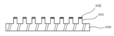
(工程(イ))
まず、図3Aに示すように、平面格子パターンの格子点に相当する柱状の凸部101が表面に形成されている転写体100を用意する。ここで、柱状とは、円柱状もしくは角柱状(三角柱、四角柱、六角柱等)である。この柱状は錐体を含む。好ましくは円柱状である。凸部101の高さは、異方性導電接続すべき端子ピッチ、端子巾、スペース巾、導電粒子の平均粒子径等に応じて決定することができるが、使用する導電粒子の平均粒子径の好ましくは1.2倍以上2倍未満である。また、凸部101の巾(半分の高さでの巾)は、導電粒子の平均粒子径の好ましくは0.7倍以上1.3倍以下である。この高さと巾がこれらの範囲であれば、脱落と抜けが連続的に発生することが避けられるという効果が得られる。
(Process (a))
First, as shown in FIG. 3A, a
更に、凸部101は、導電粒子が安定的に付着していられるようなレベルの平坦な天面を有する。
Furthermore, the
*転写体の具体例
この工程(イ)で用意すべき転写体は、公知の手法を利用して作成することができ、例えば、金属プレートを加工して原盤を作成し、それに硬化性樹脂を塗布し、硬化させて作成することができる。具体的には、平坦な金属板を切削加工して、凸部に対応した凹部を形成した転写体原盤も作成し、この原盤の凹部形成面に転写体を構成する樹脂組成物を塗布し、硬化させた後、原盤から引き離すことにより転写体が得られる。
*Specific example of transfer body The transfer body to be prepared in this step (a) can be prepared by using a known method. For example, a metal plate is processed to prepare a master, and a curable resin is added thereto. It can be prepared by coating and curing. Specifically, a flat metal plate is cut to create a transfer body master having recesses corresponding to the protrusions, and the resin composition constituting the transfer body is applied to the recess forming surface of the master, After curing, the transfer body is obtained by separating it from the master.
(工程(ロ))
次に、図3Bに示すように、表面に複数の凸部101が平面格子パターンで形成された転写体100の凸部101の少なくとも天面を微粘着層102とする。
(Process (b))
Next, as shown in FIG. 3B, at least the top surface of the
*転写体の微粘着層
微粘着層102は、異方性導電フィルムを構成する絶縁性接着ベース層に導電粒子が転着されるまで、導電粒子を一時的に保持できる粘着力を示す層であり、凸部101の少なくとも天面に形成される。従って、凸部101全体が微粘着性であってもよい。微粘着層102の厚みは、微粘着層102の材質、導電粒子の粒子径等に応じて適宜決定することができる。また、“微粘着”とは、絶縁性接着ベース層に導電粒子を転着する際に、絶縁性接着ベース層よりも粘着力が弱いという意味である。
*Slightly Adhesive Layer of Transfer Body The slightly
このような微粘着層102は、公知の異方性導電フィルムに使用されている微粘着層を適用することができる。例えば、シリコーン系の粘着剤組成物や絶縁性接着ベース層や絶縁性接着カバー層と同材質の粘着層を、凸部101の天面に塗布することにより形成することができる。
As such a slight
(工程(ハ))
次に、図3Cに示すように、転写体100の凸部101の微粘着層102に導電粒子103を付着させる。具体的には、転写体100の凸部101の上方から導電粒子103を散布し、微粘着層102に付着しなかった導電粒子103をブロアを用いて吹き飛ばせばよい。もしくは図3Cから面の方向を逆転させ、導電粒子を一面に敷き詰めた面に突起の天面を付着させてもよい。導電粒子に不要な応力を加えないためである。このように配置に必要な導電粒子のみを突起天面に付着させることで導電粒子を回収し再利用しやすくなり、開口部に導電粒子を充填し取り出す方法に比べ、経済性にも優れることになる。なお、開口部に導電粒子を充填し取り出す方法の場合、充填されなかった導電粒子には不要な応力がかかりやすくなることが懸念される。
(Process (C))
Next, as shown in FIG. 3C,
なお、図3Cでは、左半分の凸部101の巾を、右半分の凸部101よりも狭く調整している。この結果、左半分と右半分では、図3Cに示すように、導電粒子103の凝集の態様に相違点が生ずることがある。
In FIG. 3C, the width of the left half
(工程(ニ))
次に、図3Dに示すように、転写体100の導電粒子103が付着した側の表面を、異方性導電フィルムを構成すべき絶縁性接着ベース層104を重ねて押圧することにより、絶縁性接着ベース層104の片面に導電粒子103を転着させる(図3E)。この場合、転写体100を、その凸部101が下向きになるように絶縁性接着ベース層104に重ねて押圧することが好ましい。下向きにしてブロアすることで、凸部の天面に貼着されていない導電粒子を除去し易くさせるためである。
(Process (d))
Next, as shown in FIG. 3D, the surface of the
(工程(ホ))
図3Fに示すように、導電粒子103が転着した絶縁性接着ベース層104に対し、導電粒子転着面側から絶縁性接着カバー層105を積層する。これにより本発明の異方性導電フィルム200が得られる。
(Process (e))
As shown in FIG. 3F, the insulating
なお、この異方性導電フィルム200においては、平面格子パターンの一つの格子点に複数の導電粒子同士が水平方向に接触してあるいは近接して凝集配置される場合がある。これは、導電粒子を転写体の凸部の微粘着層に付着させる際に、凸部の幅(微粘着層の幅)と導電粒子の平均粒子径とが略同等の大きさのため、一つの凸部上に導電粒子が複数存在すること考え難いものの、余分な導電粒子が微粘着層の端部に付着したり、凸部から脱落しブロアーしきれなかったものが転写体の凸部間隙に残存する場合があり得るからである。
In addition, in this anisotropic
<接続構造体>
本発明の異方性導電フィルムは、第1の電子部品(例えば、ICチップ)の端子(例えばバンプ)と、第2の電子部品(例えば配線基板)の端子(例えばバンプ、パッド)との間に配置し、第1又は第2の電子部品側から熱圧着により本硬化させて異方性導電接続することにより、ショートや導通不良が抑制された、いわゆるCOG(chip on glass)やFOG(film on glass)等の接続構造体を与えることができる。
<Connection structure>
The anisotropic conductive film of the present invention is provided between a terminal (for example, a bump) of a first electronic component (for example, an IC chip) and a terminal (for example, a bump or pad) of a second electronic component (for example, a wiring board). , And the anisotropic conductive connection is performed by main curing by thermocompression bonding from the side of the first or second electronic component, so that short circuit and conduction failure are suppressed, so-called COG (chip on glass) and FOG (film). connection structure such as on glass) can be provided.
以下、本発明を具体的に説明する。 Hereinafter, the present invention will be specifically described.
実施例1
厚さ2mmのニッケルプレートを用意し、四方格子パターンで円柱状の凹部(内径5μm、深さ6μm)を形成し、転写体原盤とした。隣接凹部中心間距離は8μmであった。従って、凹部の密度は16000個/mm2であった。
Example 1
A nickel plate having a thickness of 2 mm was prepared, and cylindrical recesses (inner diameter 5 μm, depth 6 μm) were formed in a square lattice pattern to prepare a transfer body master. The distance between the centers of the adjacent recesses was 8 μm. Therefore, the density of the recesses was 16000/mm 2.
得られた転写体原盤に、フェノキシ樹脂(YP−50、新日鉄住金化学(株))60質量部、アクリレート樹脂(M208、東亞合成(株))29質量部、光重合開始剤(IRGCUR184、BASFジャパン(株))2質量部を含有する光重合性樹脂組成物を、乾燥厚みが30μmとなるようにPET(ポリエチレンテレフタレート)フィルム上に塗布し、80℃で5分間乾燥後、高圧水銀ランプにて1000mJ光照射することにより転写体を作成した。 On the obtained transfer master, 60 parts by mass of a phenoxy resin (YP-50, Nippon Steel & Sumikin Chemical Co., Ltd.), 29 parts by mass of an acrylate resin (M208, Toagosei Co., Ltd.), a photopolymerization initiator (IRGCUR184, BASF Japan Ltd.) were used. Co., Ltd.) A photopolymerizable resin composition containing 2 parts by mass was coated on a PET (polyethylene terephthalate) film so that the dry thickness was 30 μm, dried at 80° C. for 5 minutes, and then with a high pressure mercury lamp. A transfer member was prepared by irradiating with 1000 mJ light.
転写体を原盤から引き剥がし、凸部が外側になるように直径20cmのステンレス製のロールに巻き付け、このロールを、回転させながらエポキシ樹脂(jER828、三菱化学(株))70質量部とフェノキシ樹脂(YP−50、新日鉄住金化学(株))30質量部とを含有する微粘着剤組成物を、不織布に含浸させた粘着シートに接触させ、凸部の天面に微粘着剤組成物を付着させ、厚さ1μmの微粘着層を形成して転写体を得た。 Peel the transfer material from the master and wind it around a stainless steel roll with a diameter of 20 cm so that the protrusions are on the outside. While rotating this roll, 70 parts by mass of epoxy resin (jER828, Mitsubishi Chemical Corporation) and phenoxy resin are used. (YP-50, Nippon Steel & Sumikin Chemical Co., Ltd., 30 parts by mass) is brought into contact with a pressure-sensitive adhesive sheet impregnated with a non-woven fabric, and the slight pressure-sensitive adhesive composition is adhered to the top surface of the convex portion. Then, a slightly adhesive layer having a thickness of 1 μm was formed to obtain a transfer body.
この転写体の表面に、平均粒子径4μmの導電粒子(ニッケルメッキ樹脂粒子(AUL704、積水化学工業(株)))を散布した後、ブロアすることにより微粘着層に付着していないで導電粒子を除去した。 Conductive particles having an average particle diameter of 4 μm (nickel-plated resin particles (AUL704, Sekisui Chemical Co., Ltd.)) were sprayed on the surface of this transfer member, and then blown to prevent the conductive particles from adhering to the slightly adhesive layer. Was removed.
導電粒子が付着した転写体を、その導電粒子付着面から、絶縁性接着ベース層である厚さ5μmのシート状の熱硬化型の絶縁性接着フィルム(フェノキシ樹脂(YP−50、新日鉄住金化学(株))60質量部、エポキシ樹脂(jER828、三菱化学(株))40質量部、カチオン系硬化剤(SI−60L、三新化学工業(株))2質量部、及びシリカ微粒子(アエロジルRY200、日本アエロジル(株))20質量部を含有する絶縁性接着組成物から形成したフィルム)に対し、温度50℃、圧力0.5MPaで押圧することにより、絶縁性接着ベース層に導電粒子を転写させた。 From the surface where the conductive particles are adhered, the transfer body on which the conductive particles are adhered is a sheet-like thermosetting insulating adhesive film (phenoxy resin (YP-50, Nippon Steel & Sumikin Chemical ( Co., Ltd.) 60 parts by mass, epoxy resin (jER828, Mitsubishi Chemical Corporation) 40 parts by mass, cationic curing agent (SI-60L, Sanshin Chemical Industry Co., Ltd.) 2 parts by mass, and silica fine particles (Aerosil RY200, A film formed from an insulating adhesive composition containing 20 parts by mass of Nippon Aerosil Co., Ltd.) is pressed at a temperature of 50° C. and a pressure of 0.5 MPa to transfer the conductive particles to the insulating adhesive base layer. It was
得られた絶縁性接着ベース層の導電粒子転着面に、透明な絶縁性接着カバー層として厚さ15μmのシート状の別の絶縁性接着フィルム(フェノキシ樹脂(YP−50、新日鉄住金化学(株))60質量部、エポキシ樹脂(jER828、三菱化学(株))40質量部、及びカチオン系硬化剤(SI−60L、三新化学工業(株))2質量部を含有する絶縁性接着組成物から形成されたフィルム)を重ね、温度60℃、圧力2MPaで積層した。これにより異方性導電フィルムが得られた。 On the conductive particle transfer surface of the obtained insulating adhesive base layer, another sheet-like insulating adhesive film having a thickness of 15 μm as a transparent insulating adhesive cover layer (phenoxy resin (YP-50, Nippon Steel & Sumikin Chemical Co., Ltd. )) 60 parts by mass, an epoxy resin (jER828, Mitsubishi Chemical Co., Ltd.) 40 parts by mass, and a cationic curing agent (SI-60L, Sanshin Chemical Industry Co., Ltd.) 2 parts by mass of an insulating adhesive composition. Films formed from the above) were stacked and laminated at a temperature of 60° C. and a pressure of 2 MPa. As a result, an anisotropic conductive film was obtained.
実施例2
導電粒子の散布量とブロア回数とを実施例1の場合に比べてそれぞれ2倍とすること以外、実施例1を繰り返すことにより異方性導電フィルムを得た。
Example 2
An anisotropic conductive film was obtained by repeating Example 1 except that the amount of conductive particles sprayed and the number of blowers were each doubled as compared with the case of Example 1.
実施例3
転写体原盤の凹部の内径を3.6μm、隣接凹部中心間距離を6μmとして凹部の密度を28000個/mm2とし、且つ平均粒子径4μmの導電粒子に代えて平均粒子径3μmの導電粒子(AUL703、積水化学工業(株)))を使用すること以外、実施例1を繰り返すことにより異方性導電フィルムを得た。
Example 3
The inner diameter of the recesses of the master of the transfer body is 3.6 μm, the distance between the centers of adjacent recesses is 6 μm, the density of the recesses is 28,000 particles/mm 2, and conductive particles having an average particle diameter of 3 μm are used instead of the conductive particles having an average particle diameter of 4 μm (AUL703). , Sekisui Chemical Co., Ltd.) was repeated to obtain an anisotropic conductive film.
実施例4
導電粒子の散布量とブロア回数とを実施例3の場合に比べてそれぞれ2倍とすること以外、実施例3を繰り返すことにより異方性導電フィルムを得た。
Example 4
An anisotropic conductive film was obtained by repeating Example 3 except that the amount of conductive particles sprayed and the number of blowers were each doubled as compared with Example 3.
比較例1
転写体原盤の凹部の深さを4.4μm、凹部の内径を4.8μm、隣接凹部中心間距離を5.6μmとして凹部の密度を32000個/mm2とすること以外、実施例1を繰り返すことにより異方性導電フィルムを得た。
Comparative Example 1
Example 1 is repeated except that the depth of the recesses of the transfer body master is 4.4 μm, the inner diameter of the recesses is 4.8 μm, the distance between the centers of adjacent recesses is 5.6 μm, and the density of the recesses is 32000/mm 2. Thus, an anisotropic conductive film was obtained.
比較例2
転写体原盤の凹部の深さを3.3μm、凹部の内径を3.6μm、隣接凹部中心間距離を4.2μmとして凹部の密度を57000個/mm2とし、且つ平均粒子径4μmの導電粒子に代えて平均粒子径3μmの導電粒子(AUL703、積水化学工業(株))を使用すること以外、実施例1を繰り返すことにより異方性導電フィルムを得た。
Comparative example 2
Conductive particles having a recess depth of 3.3 μm, a recess inner diameter of 3.6 μm, a center-to-center distance between adjacent recesses of 4.2 μm, a recess density of 57,000 particles/mm 2 , and an average particle diameter of 4 μm. An anisotropic conductive film was obtained by repeating Example 1 except that conductive particles having an average particle diameter of 3 μm (AUL703, Sekisui Chemical Co., Ltd.) were used instead of.
<評価>
(導電粒子の「抜け」と「凝集」)
実施例1〜4及び比較例1〜2の異方性導電フィルムについて、その透明な絶縁性接着カバー層側から光学顕微鏡(MX50、オリンパス(株))で1cm四方の領域を観察し、想定される平面格子パターンにおいて導電粒子が付着していない格子点の全格子点に対する割合(抜け[%])と、2個以上の導電粒子が凝集している格子点の全格子点に対する割合とを調べた。得られた結果を表1に示す。
<Evaluation>
(“Elimination” and “Agglomeration” of conductive particles)
Regarding the anisotropic conductive films of Examples 1 to 4 and Comparative Examples 1 to 2, a 1 cm square area was observed with an optical microscope (MX50, Olympus Corporation) from the transparent insulating adhesive cover layer side, and it is assumed. The ratio of the lattice points where no conductive particles are attached to all the lattice points (missing [%]) and the ratio of the lattice points where two or more conductive particles are aggregated to all the lattice points It was The results obtained are shown in Table 1.
また、凝集した導電粒子同士の最大距離(凝集距離)を測定し、併せて表1に示した。なお、「凝集」方向は、いずれも異方性導電フィルムの水平方向であった。 Further, the maximum distance (aggregation distance) between the aggregated conductive particles was measured, and is also shown in Table 1. The "aggregation" direction was the horizontal direction of the anisotropic conductive film.
(粒子面積占有率)
導電粒子の平均粒子径と、転写体原盤の凹部密度(=転写体の凸部密度)とから、導電粒子の「抜け」と「凝集」とを考慮した上で、粒子面積占有率を計算した。得られた結果を表1に示す。
(Particle area occupation rate)
The particle area occupancy rate was calculated from the average particle diameter of the conductive particles and the concave density of the master of the transfer body (=the convex density of the transfer body) in consideration of the “dropout” and “aggregation” of the conductive particles. .. The results obtained are shown in Table 1.
(初期導通抵抗)
実施例及び比較例の異方性導電フィルムを用いて、バンプ間スペースが12μmで、高さ15μm、30×50μmの金バンプを有するICチップと、12μmスペースの配線が設けられたガラス基板とを180℃、60MPa、5秒という条件で異方性導電接続し、接続構造体を得た。得られた接続構造体について、抵抗測定器(デジタルマルチメーター7565、横河電気(株))を用いて初期導通抵抗値を測定した。得られた結果を表1に示す。0.5Ω以下であることが望まれる。
(Initial conduction resistance)
Using the anisotropic conductive films of Examples and Comparative Examples, an IC chip having a bump-to-bump space of 12 μm, a height of 15 μm, and 30×50 μm gold bumps, and a glass substrate provided with a wiring of 12 μm space were provided. Anisotropic conductive connection was performed under the conditions of 180° C., 60 MPa, and 5 seconds to obtain a connection structure. With respect to the obtained connection structure, the initial conduction resistance value was measured using a resistance meter (Digital Multimeter 7565, Yokogawa Electric Co., Ltd.). The results obtained are shown in Table 1. It is desired to be 0.5Ω or less.
(導通信頼性)
初期導通抵抗値の測定に使用した接続構造体を、温度85℃、湿度85%に設定されたエージング試験器中に投入し、500時間放置した後の導通抵抗値を、初期導通抵抗と同様に測定した。得られた結果を表1に示す。5Ω以下であることが望まれる。
(Continuity reliability)
The connection structure used for measuring the initial conduction resistance value was placed in an aging tester set to a temperature of 85° C. and a humidity of 85%, and the conduction resistance value after leaving for 500 hours was the same as the initial conduction resistance. It was measured. The results obtained are shown in Table 1. It is desired to be 5Ω or less.
(ショート発生率)
初期導通抵抗で使用したものと同じ接続構造体を作成し、隣接する配線間のショートの発生の有無を調べた。得られた結果を表1に示す。ショート発生率が50ppm以下であることが望まれる。
(Short rate)
The same connection structure as that used for the initial conduction resistance was created, and it was examined whether or not a short circuit occurred between adjacent wirings. The results obtained are shown in Table 1. It is desired that the short-circuit occurrence rate is 50 ppm or less.
表1の結果から、実施例1〜4の異方性導電フィルムを使用した接続構造体は、初期導通抵抗、導通信頼性、ショート発生率の各評価項目について、良好な結果を示したことがわかる。 From the results of Table 1, it was found that the connection structures using the anisotropic conductive films of Examples 1 to 4 showed good results for each evaluation item of initial conduction resistance, conduction reliability, and short-circuit occurrence rate. Recognize.
他方、比較例1、2の異方性導電フィルムの場合、導電粒子の「抜け」の割合は少ないものの「凝集」の割合が高すぎるため、ショートの発生率の評価が低いものであった。 On the other hand, in the case of the anisotropic conductive films of Comparative Examples 1 and 2, the percentage of “missing” of the conductive particles was small, but the percentage of “aggregation” was too high, and therefore the evaluation of the occurrence rate of short circuit was low.
実施例5
凹部密度が500個/mm2である転写原盤を使用するために隣接凹部中心間距離を調整すること以外、実施例2と同様にして転写体を作成し、更に異方性導電フィルムを作成した。得られた異方性導電フィルムについて、実施例2と同様に導電粒子の「抜け」と「凝集」とを測定し、更に粒子面積占有率を算出した。その結果、導電粒子の「抜け」と「凝集」とは実施例2と同等であった。また、粒子面積占有率は0.6%であった。
Example 5
A transfer member was prepared in the same manner as in Example 2 except that the distance between the centers of adjacent recesses was adjusted in order to use a transfer master having a recess density of 500/mm 2 , and further an anisotropic conductive film was prepared. .. With respect to the obtained anisotropic conductive film, “missing” and “aggregation” of conductive particles were measured in the same manner as in Example 2, and the particle area occupancy rate was calculated. As a result, the "dropout" and "aggregation" of the conductive particles were the same as in Example 2. The particle area occupation rate was 0.6%.
また、得られた異方性導電フィルムを、ガラス基板(ITOベタ電極)とフレキシブル配線基板(バンプ幅:200μm、L(ライン)/S(スペース)=1、配線高さ10μm)との間に挟み、接続バンプ長さが1mmとなるように、180℃、80MPa、5秒という条件で異方性導電し、評価用の接続構造体を得た。得られた接続構造体について、その「初期導通抵抗値」と、温度85℃で湿度85%RHの恒温槽に500時間投入した後の「導通信頼性」とを、デジタルマルチメータ(34401A、アジレント・テクノロジー株式会社製)を使用して電流1Aで4端子法にて導通抵抗を測定し、「初期導通抵抗値」の場合には、測定値が2Ω以下の場合を良好、2Ωを超えるものを不良と評価し、「導通信頼性」の場合には、測定値が5Ω以下の場合を良好、5Ω以上の場合を不良と評価した。その結果、実施例5の接続構造体は、いずれも「良好」と評価された。また、実施例2と同様に「ショート発生率」を測定したところ、実施例2と同様に良好な結果が得られた。
In addition, the obtained anisotropic conductive film was placed between a glass substrate (ITO solid electrode) and a flexible wiring substrate (bump width: 200 μm, L (line)/S (space)=1,
実施例6
凹部密度が2000個/mm2である転写原盤を使用するために隣接凹部中心間距離を調整すること以外、実施例2と同様にして転写体を作成し、更に異方性導電フィルムを作成した。得られた異方性導電フィルムについて、実施例2と同様に導電粒子の「抜け」と「凝集」とを測定し、更に粒子面積占有率を算出した。その結果、導電粒子の「抜け」と「凝集」とは実施例2と同等であった。また、粒子面積占有率は2.4%であった。
Example 6
A transfer member was prepared in the same manner as in Example 2 except that the distance between the centers of the adjacent recesses was adjusted in order to use a transfer master having a recess density of 2000/mm 2 , and further an anisotropic conductive film was prepared. .. With respect to the obtained anisotropic conductive film, “missing” and “aggregation” of conductive particles were measured in the same manner as in Example 2, and the particle area occupancy rate was calculated. As a result, the "dropout" and "aggregation" of the conductive particles were the same as in Example 2. The particle area occupancy rate was 2.4%.
また、得られた異方性導電フィルムを、実施例5と同様にガラス基板とフレキシブル配線基板との間に挟み異方性導電接続することにより評価用の接続構造体を得た。得られた接続構造体について、実施例5と同様に、「初期導通抵抗値」、「導通信頼性」、「ショート発生率」とを評価したところ、いずれも良好な結果が得られた。 In addition, the obtained anisotropic conductive film was sandwiched between a glass substrate and a flexible wiring substrate and anisotropically conductively connected in the same manner as in Example 5 to obtain a connection structure for evaluation. The obtained connection structure was evaluated for "initial conduction resistance value", "conduction reliability", and "short circuit occurrence rate" in the same manner as in Example 5, and good results were obtained.
本発明の好ましい異方性導電フィルムにおいては、基準領域に想定される平面格子パターンの全格子点に対する「導電粒子が配置されていない格子点」の割合が20%未満に設定され、しかも平面格子パターンの全格子点に対する「複数の導電粒子が凝集して配置されている格子点」の割合が5%以下である。このため、本発明の異方性導電フィルムを異方性導電接続に適用した場合、良好な初期導通性とエージング後の良好な導通信頼性とを実現でき、ショートの発生も抑制できるので、狭ピッチ化したICチップと配線基板とを、異方性導電接続する場合に有用である。 In the preferred anisotropic conductive film of the present invention, the ratio of "lattice points where conductive particles are not arranged" to all the lattice points of the plane lattice pattern assumed in the reference region is set to less than 20%, and the plane lattice is also used. The ratio of “lattice points where a plurality of conductive particles are aggregated and arranged” to all the lattice points of the pattern is 5% or less. Therefore, when the anisotropic conductive film of the present invention is applied to anisotropic conductive connection, good initial conductivity and good conductivity reliability after aging can be realized, and the occurrence of short circuits can be suppressed. This is useful when anisotropically conductively connecting a pitched IC chip and a wiring board.
10、200 異方性導電フィルム
11、104 絶縁性接着ベース層
12、105 絶縁性接着カバー層
13、103 導電粒子
100 転写体
101 凸部
102 微粘着層
A 導電粒子が抜けている格子点
B 導電粒子が互いに接して凝集している格子点
C 導電粒子が互いに離間して凝集している格子点
10, 200 Anisotropic
Claims (13)
<工程(イ)>
平面格子パターンの格子点に相当する柱状の凸部が表面に形成された転写体を用意する工程;
<工程(ロ)>
転写体の凸部の少なくとも天面を微粘着層とする工程;
<工程(ハ)>
該転写体の凸部の微粘着層に導電粒子を付着させる工程;
<工程(ニ)>
該転写体の導電粒子が付着した側の表面に絶縁性接着ベース層を重ねて押圧することにより、絶縁性接着ベース層に導電粒子を転着させる工程;及び
<工程(ホ)>
導電粒子が転着した絶縁性接着ベース層に対し、導電粒子転着面側から絶縁性接着カバー層を積層する工程
を有する製造方法。 The insulating adhesive base layer has a structure in which conductive particles are arranged at lattice points of a plane lattice pattern, and conductive particles are arranged at all lattice points of the plane lattice pattern assumed in the reference area of the anisotropic conductive film. The ratio of the non-existing grid points is less than 20%, and the ratio of the grid points in which the plurality of conductive particles are aggregated and arranged with respect to all the grid points of the planar lattice pattern is 15% or less. A method for producing an anisotropic conductive film , the total of which is less than 25% , comprising the following steps (a) to (e):
<Process (a)>
A step of preparing a transfer body having columnar convex portions corresponding to lattice points of a plane lattice pattern formed on the surface;
<Process (b)>
A step of forming a slight adhesive layer on at least the top surface of the convex portion of the transfer member;
<Process (C)>
A step of attaching conductive particles to the slightly adhesive layer on the convex portion of the transfer member;
<Process (d)>
A step of transferring the conductive particles to the insulating adhesive base layer by stacking and pressing the insulating adhesive base layer on the surface of the transfer body on which the conductive particles adhere; and <step (e)>
A method of manufacturing, comprising a step of laminating an insulating adhesive cover layer from the conductive particle transfer surface side to an insulating adhesive base layer on which conductive particles are transferred.
<工程(イ)>
平面格子パターンの格子点に相当する柱状の凸部が表面に形成された転写体を用意する工程;
<工程(ロ)>
転写体の凸部の少なくとも天面を微粘着層とする工程;
<工程(ハ)>
該転写体の凸部の微粘着層に導電粒子を付着させる工程;及び
<工程(ニ)>
該転写体の導電粒子が付着した側の表面に絶縁性接着ベース層を重ねて押圧することにより、絶縁性接着ベース層に導電粒子を転着させる工程
を有する製造方法。 The insulating adhesive base layer has a structure in which conductive particles are arranged at lattice points of a plane lattice pattern, and conductive particles are arranged at all lattice points of the plane lattice pattern assumed in the reference area of the anisotropic conductive film. The ratio of the non-existing grid points is less than 20%, and the ratio of the grid points in which the plurality of conductive particles are aggregated and arranged with respect to all the grid points of the planar lattice pattern is 15% or less. A method for producing an anisotropic conductive film having a total content of less than 25% , comprising the following steps (a) to (d):
<Process (a)>
A step of preparing a transfer body having columnar convex portions corresponding to lattice points of a plane lattice pattern formed on the surface;
<Process (b)>
A step of forming a slight adhesive layer on at least the top surface of the convex portion of the transfer member;
<Process (C)>
A step of attaching conductive particles to the slightly adhesive layer on the convex portion of the transfer member; and <step (d)>
A manufacturing method comprising a step of transferring conductive particles to the insulating adhesive base layer by stacking and pressing the insulating adhesive base layer on the surface of the transfer body on which the conductive particles are attached.
<工程(イ)>
平面格子パターンに相当する凸部が表面に形成された転写体を用意する工程;
<工程(ロ)>
転写体の凸部の少なくとも天面を微粘着層とする工程;
<工程(ハ)>
該転写体の凸部の微粘着層に導電粒子を付着させる工程;及び
<工程(ニ)>
該転写体の導電粒子が付着した側の表面に絶縁性接着ベース層を重ねて押圧することにより、絶縁性接着ベース層に導電粒子を転着させる工程
を有する製造方法。 An anisotropic conductive film having a structure in which conductive particles are arranged in a plane lattice pattern in the insulating adhesive base layer, and the conductive particles are not arranged for the plane lattice pattern assumed in the reference region of the anisotropic conductive film. Anisotropic conductivity having a ratio of less than 20%, a ratio of a plurality of conductive particles aggregated and arranged with respect to the planar lattice pattern is 15% or less, and a total of voids and agglomeration is less than 25%. A method for producing a film, comprising the following steps (a) to (d):
<Process (a)>
A step of preparing a transfer body on the surface of which projections corresponding to a plane lattice pattern are formed;
<Process (b)>
A step of forming a slight adhesive layer on at least the top surface of the convex portion of the transfer member;
<Process (C)>
A step of attaching conductive particles to the slightly adhesive layer on the convex portion of the transfer member; and <step (d)>
A manufacturing method comprising a step of transferring conductive particles to the insulating adhesive base layer by stacking and pressing the insulating adhesive base layer on the surface of the transfer body on which the conductive particles are attached.
Applications Claiming Priority (2)
| Application Number | Priority Date | Filing Date | Title |
|---|---|---|---|
| JP2014219790 | 2014-10-28 | ||
| JP2014219790 | 2014-10-28 |
Related Child Applications (1)
| Application Number | Title | Priority Date | Filing Date |
|---|---|---|---|
| JP2020088028A Division JP7067586B2 (en) | 2014-10-28 | 2020-05-20 | Anisotropic conductive film |
Publications (3)
| Publication Number | Publication Date |
|---|---|
| JP2016085984A JP2016085984A (en) | 2016-05-19 |
| JP2016085984A5 JP2016085984A5 (en) | 2018-11-29 |
| JP6707835B2 true JP6707835B2 (en) | 2020-06-10 |
Family
ID=55973228
Family Applications (3)
| Application Number | Title | Priority Date | Filing Date |
|---|---|---|---|
| JP2015211452A Active JP6707835B2 (en) | 2014-10-28 | 2015-10-28 | Anisotropic conductive film |
| JP2020088028A Active JP7067586B2 (en) | 2014-10-28 | 2020-05-20 | Anisotropic conductive film |
| JP2022074596A Active JP7348563B2 (en) | 2014-10-28 | 2022-04-28 | Anisotropic conductive film |
Family Applications After (2)
| Application Number | Title | Priority Date | Filing Date |
|---|---|---|---|
| JP2020088028A Active JP7067586B2 (en) | 2014-10-28 | 2020-05-20 | Anisotropic conductive film |
| JP2022074596A Active JP7348563B2 (en) | 2014-10-28 | 2022-04-28 | Anisotropic conductive film |
Country Status (1)
| Country | Link |
|---|---|
| JP (3) | JP6707835B2 (en) |
Families Citing this family (2)
| Publication number | Priority date | Publication date | Assignee | Title |
|---|---|---|---|---|
| JP2018006160A (en) * | 2016-07-01 | 2018-01-11 | 古河電気工業株式会社 | Wire with terminal and manufacturing method thereof |
| CN109964371B (en) | 2016-12-01 | 2021-03-12 | 迪睿合株式会社 | Anisotropic conductive film |
Family Cites Families (5)
| Publication number | Priority date | Publication date | Assignee | Title |
|---|---|---|---|---|
| US20010008169A1 (en) | 1998-06-30 | 2001-07-19 | 3M Innovative Properties Company | Fine pitch anisotropic conductive adhesive |
| JP3694825B2 (en) | 1999-11-18 | 2005-09-14 | 日本航空電子工業株式会社 | Conductive pattern forming method and connector, flexible printed wiring board, anisotropic conductive member |
| JP4865144B2 (en) | 2001-05-08 | 2012-02-01 | 旭化成株式会社 | Method for arranging particles in an adhesive layer |
| JP4130747B2 (en) * | 2002-03-28 | 2008-08-06 | 旭化成エレクトロニクス株式会社 | Anisotropic conductive adhesive sheet and manufacturing method thereof |
| JP2010033793A (en) | 2008-07-28 | 2010-02-12 | Tokai Rubber Ind Ltd | Method for manufacturing particle transfer film |
-
2015
- 2015-10-28 JP JP2015211452A patent/JP6707835B2/en active Active
-
2020
- 2020-05-20 JP JP2020088028A patent/JP7067586B2/en active Active
-
2022
- 2022-04-28 JP JP2022074596A patent/JP7348563B2/en active Active
Also Published As
| Publication number | Publication date |
|---|---|
| JP2020129559A (en) | 2020-08-27 |
| JP2022097589A (en) | 2022-06-30 |
| JP7067586B2 (en) | 2022-05-16 |
| JP2016085984A (en) | 2016-05-19 |
| JP7348563B2 (en) | 2023-09-21 |
Similar Documents
| Publication | Publication Date | Title |
|---|---|---|
| JP7140162B2 (en) | anisotropic conductive film | |
| JP6750205B2 (en) | Anisotropic conductive film | |
| KR102240963B1 (en) | Anisotropic conductive film, manufacturing method for same, and connection structure | |
| JP7348563B2 (en) | Anisotropic conductive film | |
| JP2023001188A (en) | Anisotropically conductive film | |
| JP6962404B2 (en) | Anisotropic conductive film | |
| JP6682804B2 (en) | Anisotropic conductive film |
Legal Events
| Date | Code | Title | Description |
|---|---|---|---|
| A521 | Request for written amendment filed |
Free format text: JAPANESE INTERMEDIATE CODE: A523 Effective date: 20181017 |
|
| A621 | Written request for application examination |
Free format text: JAPANESE INTERMEDIATE CODE: A621 Effective date: 20181017 |
|
| A977 | Report on retrieval |
Free format text: JAPANESE INTERMEDIATE CODE: A971007 Effective date: 20190621 |
|
| A131 | Notification of reasons for refusal |
Free format text: JAPANESE INTERMEDIATE CODE: A131 Effective date: 20190709 |
|
| A601 | Written request for extension of time |
Free format text: JAPANESE INTERMEDIATE CODE: A601 Effective date: 20190905 |
|
| A521 | Request for written amendment filed |
Free format text: JAPANESE INTERMEDIATE CODE: A523 Effective date: 20191105 |
|
| TRDD | Decision of grant or rejection written | ||
| A01 | Written decision to grant a patent or to grant a registration (utility model) |
Free format text: JAPANESE INTERMEDIATE CODE: A01 Effective date: 20200421 |
|
| A61 | First payment of annual fees (during grant procedure) |
Free format text: JAPANESE INTERMEDIATE CODE: A61 Effective date: 20200504 |
|
| R150 | Certificate of patent or registration of utility model |
Ref document number: 6707835 Country of ref document: JP Free format text: JAPANESE INTERMEDIATE CODE: R150 |
|
| R250 | Receipt of annual fees |
Free format text: JAPANESE INTERMEDIATE CODE: R250 |