JP6704724B2 - Display device - Google Patents
Display device Download PDFInfo
- Publication number
- JP6704724B2 JP6704724B2 JP2015245376A JP2015245376A JP6704724B2 JP 6704724 B2 JP6704724 B2 JP 6704724B2 JP 2015245376 A JP2015245376 A JP 2015245376A JP 2015245376 A JP2015245376 A JP 2015245376A JP 6704724 B2 JP6704724 B2 JP 6704724B2
- Authority
- JP
- Japan
- Prior art keywords
- substrate
- insulating film
- display device
- insulating
- region
- Prior art date
- Legal status (The legal status is an assumption and is not a legal conclusion. Google has not performed a legal analysis and makes no representation as to the accuracy of the status listed.)
- Active
Links
Images


Classifications
-
- G—PHYSICS
- G02—OPTICS
- G02F—OPTICAL DEVICES OR ARRANGEMENTS FOR THE CONTROL OF LIGHT BY MODIFICATION OF THE OPTICAL PROPERTIES OF THE MEDIA OF THE ELEMENTS INVOLVED THEREIN; NON-LINEAR OPTICS; FREQUENCY-CHANGING OF LIGHT; OPTICAL LOGIC ELEMENTS; OPTICAL ANALOGUE/DIGITAL CONVERTERS
- G02F1/00—Devices or arrangements for the control of the intensity, colour, phase, polarisation or direction of light arriving from an independent light source, e.g. switching, gating or modulating; Non-linear optics
- G02F1/01—Devices or arrangements for the control of the intensity, colour, phase, polarisation or direction of light arriving from an independent light source, e.g. switching, gating or modulating; Non-linear optics for the control of the intensity, phase, polarisation or colour
- G02F1/13—Devices or arrangements for the control of the intensity, colour, phase, polarisation or direction of light arriving from an independent light source, e.g. switching, gating or modulating; Non-linear optics for the control of the intensity, phase, polarisation or colour based on liquid crystals, e.g. single liquid crystal display cells
- G02F1/133—Constructional arrangements; Operation of liquid crystal cells; Circuit arrangements
- G02F1/1333—Constructional arrangements; Manufacturing methods
- G02F1/133345—Insulating layers
-
- G—PHYSICS
- G02—OPTICS
- G02F—OPTICAL DEVICES OR ARRANGEMENTS FOR THE CONTROL OF LIGHT BY MODIFICATION OF THE OPTICAL PROPERTIES OF THE MEDIA OF THE ELEMENTS INVOLVED THEREIN; NON-LINEAR OPTICS; FREQUENCY-CHANGING OF LIGHT; OPTICAL LOGIC ELEMENTS; OPTICAL ANALOGUE/DIGITAL CONVERTERS
- G02F1/00—Devices or arrangements for the control of the intensity, colour, phase, polarisation or direction of light arriving from an independent light source, e.g. switching, gating or modulating; Non-linear optics
- G02F1/01—Devices or arrangements for the control of the intensity, colour, phase, polarisation or direction of light arriving from an independent light source, e.g. switching, gating or modulating; Non-linear optics for the control of the intensity, phase, polarisation or colour
- G02F1/13—Devices or arrangements for the control of the intensity, colour, phase, polarisation or direction of light arriving from an independent light source, e.g. switching, gating or modulating; Non-linear optics for the control of the intensity, phase, polarisation or colour based on liquid crystals, e.g. single liquid crystal display cells
- G02F1/133—Constructional arrangements; Operation of liquid crystal cells; Circuit arrangements
- G02F1/1333—Constructional arrangements; Manufacturing methods
- G02F1/1345—Conductors connecting electrodes to cell terminals
- G02F1/13452—Conductors connecting driver circuitry and terminals of panels
-
- G—PHYSICS
- G02—OPTICS
- G02F—OPTICAL DEVICES OR ARRANGEMENTS FOR THE CONTROL OF LIGHT BY MODIFICATION OF THE OPTICAL PROPERTIES OF THE MEDIA OF THE ELEMENTS INVOLVED THEREIN; NON-LINEAR OPTICS; FREQUENCY-CHANGING OF LIGHT; OPTICAL LOGIC ELEMENTS; OPTICAL ANALOGUE/DIGITAL CONVERTERS
- G02F1/00—Devices or arrangements for the control of the intensity, colour, phase, polarisation or direction of light arriving from an independent light source, e.g. switching, gating or modulating; Non-linear optics
- G02F1/01—Devices or arrangements for the control of the intensity, colour, phase, polarisation or direction of light arriving from an independent light source, e.g. switching, gating or modulating; Non-linear optics for the control of the intensity, phase, polarisation or colour
- G02F1/13—Devices or arrangements for the control of the intensity, colour, phase, polarisation or direction of light arriving from an independent light source, e.g. switching, gating or modulating; Non-linear optics for the control of the intensity, phase, polarisation or colour based on liquid crystals, e.g. single liquid crystal display cells
- G02F1/133—Constructional arrangements; Operation of liquid crystal cells; Circuit arrangements
- G02F1/1333—Constructional arrangements; Manufacturing methods
- G02F1/133308—Support structures for LCD panels, e.g. frames or bezels
-
- G—PHYSICS
- G02—OPTICS
- G02F—OPTICAL DEVICES OR ARRANGEMENTS FOR THE CONTROL OF LIGHT BY MODIFICATION OF THE OPTICAL PROPERTIES OF THE MEDIA OF THE ELEMENTS INVOLVED THEREIN; NON-LINEAR OPTICS; FREQUENCY-CHANGING OF LIGHT; OPTICAL LOGIC ELEMENTS; OPTICAL ANALOGUE/DIGITAL CONVERTERS
- G02F1/00—Devices or arrangements for the control of the intensity, colour, phase, polarisation or direction of light arriving from an independent light source, e.g. switching, gating or modulating; Non-linear optics
- G02F1/01—Devices or arrangements for the control of the intensity, colour, phase, polarisation or direction of light arriving from an independent light source, e.g. switching, gating or modulating; Non-linear optics for the control of the intensity, phase, polarisation or colour
- G02F1/13—Devices or arrangements for the control of the intensity, colour, phase, polarisation or direction of light arriving from an independent light source, e.g. switching, gating or modulating; Non-linear optics for the control of the intensity, phase, polarisation or colour based on liquid crystals, e.g. single liquid crystal display cells
- G02F1/133—Constructional arrangements; Operation of liquid crystal cells; Circuit arrangements
- G02F1/1333—Constructional arrangements; Manufacturing methods
- G02F1/1335—Structural association of cells with optical devices, e.g. polarisers or reflectors
- G02F1/133509—Filters, e.g. light shielding masks
- G02F1/133512—Light shielding layers, e.g. black matrix
-
- G—PHYSICS
- G02—OPTICS
- G02F—OPTICAL DEVICES OR ARRANGEMENTS FOR THE CONTROL OF LIGHT BY MODIFICATION OF THE OPTICAL PROPERTIES OF THE MEDIA OF THE ELEMENTS INVOLVED THEREIN; NON-LINEAR OPTICS; FREQUENCY-CHANGING OF LIGHT; OPTICAL LOGIC ELEMENTS; OPTICAL ANALOGUE/DIGITAL CONVERTERS
- G02F1/00—Devices or arrangements for the control of the intensity, colour, phase, polarisation or direction of light arriving from an independent light source, e.g. switching, gating or modulating; Non-linear optics
- G02F1/01—Devices or arrangements for the control of the intensity, colour, phase, polarisation or direction of light arriving from an independent light source, e.g. switching, gating or modulating; Non-linear optics for the control of the intensity, phase, polarisation or colour
- G02F1/13—Devices or arrangements for the control of the intensity, colour, phase, polarisation or direction of light arriving from an independent light source, e.g. switching, gating or modulating; Non-linear optics for the control of the intensity, phase, polarisation or colour based on liquid crystals, e.g. single liquid crystal display cells
- G02F1/133—Constructional arrangements; Operation of liquid crystal cells; Circuit arrangements
- G02F1/1333—Constructional arrangements; Manufacturing methods
- G02F1/1339—Gaskets; Spacers; Sealing of cells
-
- G—PHYSICS
- G02—OPTICS
- G02F—OPTICAL DEVICES OR ARRANGEMENTS FOR THE CONTROL OF LIGHT BY MODIFICATION OF THE OPTICAL PROPERTIES OF THE MEDIA OF THE ELEMENTS INVOLVED THEREIN; NON-LINEAR OPTICS; FREQUENCY-CHANGING OF LIGHT; OPTICAL LOGIC ELEMENTS; OPTICAL ANALOGUE/DIGITAL CONVERTERS
- G02F1/00—Devices or arrangements for the control of the intensity, colour, phase, polarisation or direction of light arriving from an independent light source, e.g. switching, gating or modulating; Non-linear optics
- G02F1/01—Devices or arrangements for the control of the intensity, colour, phase, polarisation or direction of light arriving from an independent light source, e.g. switching, gating or modulating; Non-linear optics for the control of the intensity, phase, polarisation or colour
- G02F1/13—Devices or arrangements for the control of the intensity, colour, phase, polarisation or direction of light arriving from an independent light source, e.g. switching, gating or modulating; Non-linear optics for the control of the intensity, phase, polarisation or colour based on liquid crystals, e.g. single liquid crystal display cells
- G02F1/133—Constructional arrangements; Operation of liquid crystal cells; Circuit arrangements
- G02F1/1333—Constructional arrangements; Manufacturing methods
- G02F1/1343—Electrodes
- G02F1/134309—Electrodes characterised by their geometrical arrangement
-
- G—PHYSICS
- G02—OPTICS
- G02F—OPTICAL DEVICES OR ARRANGEMENTS FOR THE CONTROL OF LIGHT BY MODIFICATION OF THE OPTICAL PROPERTIES OF THE MEDIA OF THE ELEMENTS INVOLVED THEREIN; NON-LINEAR OPTICS; FREQUENCY-CHANGING OF LIGHT; OPTICAL LOGIC ELEMENTS; OPTICAL ANALOGUE/DIGITAL CONVERTERS
- G02F1/00—Devices or arrangements for the control of the intensity, colour, phase, polarisation or direction of light arriving from an independent light source, e.g. switching, gating or modulating; Non-linear optics
- G02F1/01—Devices or arrangements for the control of the intensity, colour, phase, polarisation or direction of light arriving from an independent light source, e.g. switching, gating or modulating; Non-linear optics for the control of the intensity, phase, polarisation or colour
- G02F1/13—Devices or arrangements for the control of the intensity, colour, phase, polarisation or direction of light arriving from an independent light source, e.g. switching, gating or modulating; Non-linear optics for the control of the intensity, phase, polarisation or colour based on liquid crystals, e.g. single liquid crystal display cells
- G02F1/133—Constructional arrangements; Operation of liquid crystal cells; Circuit arrangements
- G02F1/1333—Constructional arrangements; Manufacturing methods
- G02F1/1343—Electrodes
- G02F1/13439—Electrodes characterised by their electrical, optical, physical properties; materials therefor; method of making
-
- G—PHYSICS
- G02—OPTICS
- G02F—OPTICAL DEVICES OR ARRANGEMENTS FOR THE CONTROL OF LIGHT BY MODIFICATION OF THE OPTICAL PROPERTIES OF THE MEDIA OF THE ELEMENTS INVOLVED THEREIN; NON-LINEAR OPTICS; FREQUENCY-CHANGING OF LIGHT; OPTICAL LOGIC ELEMENTS; OPTICAL ANALOGUE/DIGITAL CONVERTERS
- G02F1/00—Devices or arrangements for the control of the intensity, colour, phase, polarisation or direction of light arriving from an independent light source, e.g. switching, gating or modulating; Non-linear optics
- G02F1/01—Devices or arrangements for the control of the intensity, colour, phase, polarisation or direction of light arriving from an independent light source, e.g. switching, gating or modulating; Non-linear optics for the control of the intensity, phase, polarisation or colour
- G02F1/13—Devices or arrangements for the control of the intensity, colour, phase, polarisation or direction of light arriving from an independent light source, e.g. switching, gating or modulating; Non-linear optics for the control of the intensity, phase, polarisation or colour based on liquid crystals, e.g. single liquid crystal display cells
- G02F1/133—Constructional arrangements; Operation of liquid crystal cells; Circuit arrangements
- G02F1/1333—Constructional arrangements; Manufacturing methods
- G02F1/1345—Conductors connecting electrodes to cell terminals
- G02F1/13454—Drivers integrated on the active matrix substrate
-
- G—PHYSICS
- G02—OPTICS
- G02F—OPTICAL DEVICES OR ARRANGEMENTS FOR THE CONTROL OF LIGHT BY MODIFICATION OF THE OPTICAL PROPERTIES OF THE MEDIA OF THE ELEMENTS INVOLVED THEREIN; NON-LINEAR OPTICS; FREQUENCY-CHANGING OF LIGHT; OPTICAL LOGIC ELEMENTS; OPTICAL ANALOGUE/DIGITAL CONVERTERS
- G02F1/00—Devices or arrangements for the control of the intensity, colour, phase, polarisation or direction of light arriving from an independent light source, e.g. switching, gating or modulating; Non-linear optics
- G02F1/01—Devices or arrangements for the control of the intensity, colour, phase, polarisation or direction of light arriving from an independent light source, e.g. switching, gating or modulating; Non-linear optics for the control of the intensity, phase, polarisation or colour
- G02F1/13—Devices or arrangements for the control of the intensity, colour, phase, polarisation or direction of light arriving from an independent light source, e.g. switching, gating or modulating; Non-linear optics for the control of the intensity, phase, polarisation or colour based on liquid crystals, e.g. single liquid crystal display cells
- G02F1/133—Constructional arrangements; Operation of liquid crystal cells; Circuit arrangements
- G02F1/1333—Constructional arrangements; Manufacturing methods
- G02F1/1345—Conductors connecting electrodes to cell terminals
- G02F1/13458—Terminal pads
-
- H—ELECTRICITY
- H10—SEMICONDUCTOR DEVICES; ELECTRIC SOLID-STATE DEVICES NOT OTHERWISE PROVIDED FOR
- H10K—ORGANIC ELECTRIC SOLID-STATE DEVICES
- H10K50/00—Organic light-emitting devices
- H10K50/80—Constructional details
- H10K50/84—Passivation; Containers; Encapsulations
- H10K50/842—Containers
- H10K50/8426—Peripheral sealing arrangements, e.g. adhesives, sealants
-
- H—ELECTRICITY
- H10—SEMICONDUCTOR DEVICES; ELECTRIC SOLID-STATE DEVICES NOT OTHERWISE PROVIDED FOR
- H10K—ORGANIC ELECTRIC SOLID-STATE DEVICES
- H10K59/00—Integrated devices, or assemblies of multiple devices, comprising at least one organic light-emitting element covered by group H10K50/00
- H10K59/10—OLED displays
- H10K59/12—Active-matrix OLED [AMOLED] displays
- H10K59/131—Interconnections, e.g. wiring lines or terminals
-
- H—ELECTRICITY
- H10—SEMICONDUCTOR DEVICES; ELECTRIC SOLID-STATE DEVICES NOT OTHERWISE PROVIDED FOR
- H10K—ORGANIC ELECTRIC SOLID-STATE DEVICES
- H10K71/00—Manufacture or treatment specially adapted for the organic devices covered by this subclass
-
- H—ELECTRICITY
- H10—SEMICONDUCTOR DEVICES; ELECTRIC SOLID-STATE DEVICES NOT OTHERWISE PROVIDED FOR
- H10K—ORGANIC ELECTRIC SOLID-STATE DEVICES
- H10K77/00—Constructional details of devices covered by this subclass and not covered by groups H10K10/80, H10K30/80, H10K50/80 or H10K59/80
- H10K77/10—Substrates, e.g. flexible substrates
-
- G—PHYSICS
- G02—OPTICS
- G02F—OPTICAL DEVICES OR ARRANGEMENTS FOR THE CONTROL OF LIGHT BY MODIFICATION OF THE OPTICAL PROPERTIES OF THE MEDIA OF THE ELEMENTS INVOLVED THEREIN; NON-LINEAR OPTICS; FREQUENCY-CHANGING OF LIGHT; OPTICAL LOGIC ELEMENTS; OPTICAL ANALOGUE/DIGITAL CONVERTERS
- G02F1/00—Devices or arrangements for the control of the intensity, colour, phase, polarisation or direction of light arriving from an independent light source, e.g. switching, gating or modulating; Non-linear optics
- G02F1/01—Devices or arrangements for the control of the intensity, colour, phase, polarisation or direction of light arriving from an independent light source, e.g. switching, gating or modulating; Non-linear optics for the control of the intensity, phase, polarisation or colour
- G02F1/13—Devices or arrangements for the control of the intensity, colour, phase, polarisation or direction of light arriving from an independent light source, e.g. switching, gating or modulating; Non-linear optics for the control of the intensity, phase, polarisation or colour based on liquid crystals, e.g. single liquid crystal display cells
- G02F1/133—Constructional arrangements; Operation of liquid crystal cells; Circuit arrangements
- G02F1/1333—Constructional arrangements; Manufacturing methods
- G02F1/133368—Cells having two substrates with different characteristics, e.g. different thickness or material
-
- G—PHYSICS
- G02—OPTICS
- G02F—OPTICAL DEVICES OR ARRANGEMENTS FOR THE CONTROL OF LIGHT BY MODIFICATION OF THE OPTICAL PROPERTIES OF THE MEDIA OF THE ELEMENTS INVOLVED THEREIN; NON-LINEAR OPTICS; FREQUENCY-CHANGING OF LIGHT; OPTICAL LOGIC ELEMENTS; OPTICAL ANALOGUE/DIGITAL CONVERTERS
- G02F1/00—Devices or arrangements for the control of the intensity, colour, phase, polarisation or direction of light arriving from an independent light source, e.g. switching, gating or modulating; Non-linear optics
- G02F1/01—Devices or arrangements for the control of the intensity, colour, phase, polarisation or direction of light arriving from an independent light source, e.g. switching, gating or modulating; Non-linear optics for the control of the intensity, phase, polarisation or colour
- G02F1/13—Devices or arrangements for the control of the intensity, colour, phase, polarisation or direction of light arriving from an independent light source, e.g. switching, gating or modulating; Non-linear optics for the control of the intensity, phase, polarisation or colour based on liquid crystals, e.g. single liquid crystal display cells
- G02F1/133—Constructional arrangements; Operation of liquid crystal cells; Circuit arrangements
- G02F1/1333—Constructional arrangements; Manufacturing methods
- G02F1/133388—Constructional arrangements; Manufacturing methods with constructional differences between the display region and the peripheral region
-
- G—PHYSICS
- G02—OPTICS
- G02F—OPTICAL DEVICES OR ARRANGEMENTS FOR THE CONTROL OF LIGHT BY MODIFICATION OF THE OPTICAL PROPERTIES OF THE MEDIA OF THE ELEMENTS INVOLVED THEREIN; NON-LINEAR OPTICS; FREQUENCY-CHANGING OF LIGHT; OPTICAL LOGIC ELEMENTS; OPTICAL ANALOGUE/DIGITAL CONVERTERS
- G02F1/00—Devices or arrangements for the control of the intensity, colour, phase, polarisation or direction of light arriving from an independent light source, e.g. switching, gating or modulating; Non-linear optics
- G02F1/01—Devices or arrangements for the control of the intensity, colour, phase, polarisation or direction of light arriving from an independent light source, e.g. switching, gating or modulating; Non-linear optics for the control of the intensity, phase, polarisation or colour
- G02F1/13—Devices or arrangements for the control of the intensity, colour, phase, polarisation or direction of light arriving from an independent light source, e.g. switching, gating or modulating; Non-linear optics for the control of the intensity, phase, polarisation or colour based on liquid crystals, e.g. single liquid crystal display cells
- G02F1/133—Constructional arrangements; Operation of liquid crystal cells; Circuit arrangements
- G02F1/1333—Constructional arrangements; Manufacturing methods
- G02F1/1335—Structural association of cells with optical devices, e.g. polarisers or reflectors
- G02F1/133509—Filters, e.g. light shielding masks
- G02F1/133514—Colour filters
- G02F1/133519—Overcoatings
-
- G—PHYSICS
- G02—OPTICS
- G02F—OPTICAL DEVICES OR ARRANGEMENTS FOR THE CONTROL OF LIGHT BY MODIFICATION OF THE OPTICAL PROPERTIES OF THE MEDIA OF THE ELEMENTS INVOLVED THEREIN; NON-LINEAR OPTICS; FREQUENCY-CHANGING OF LIGHT; OPTICAL LOGIC ELEMENTS; OPTICAL ANALOGUE/DIGITAL CONVERTERS
- G02F1/00—Devices or arrangements for the control of the intensity, colour, phase, polarisation or direction of light arriving from an independent light source, e.g. switching, gating or modulating; Non-linear optics
- G02F1/01—Devices or arrangements for the control of the intensity, colour, phase, polarisation or direction of light arriving from an independent light source, e.g. switching, gating or modulating; Non-linear optics for the control of the intensity, phase, polarisation or colour
- G02F1/13—Devices or arrangements for the control of the intensity, colour, phase, polarisation or direction of light arriving from an independent light source, e.g. switching, gating or modulating; Non-linear optics for the control of the intensity, phase, polarisation or colour based on liquid crystals, e.g. single liquid crystal display cells
- G02F1/133—Constructional arrangements; Operation of liquid crystal cells; Circuit arrangements
- G02F1/136—Liquid crystal cells structurally associated with a semi-conducting layer or substrate, e.g. cells forming part of an integrated circuit
- G02F1/1362—Active matrix addressed cells
- G02F1/136286—Wiring, e.g. gate line, drain line
-
- G—PHYSICS
- G02—OPTICS
- G02F—OPTICAL DEVICES OR ARRANGEMENTS FOR THE CONTROL OF LIGHT BY MODIFICATION OF THE OPTICAL PROPERTIES OF THE MEDIA OF THE ELEMENTS INVOLVED THEREIN; NON-LINEAR OPTICS; FREQUENCY-CHANGING OF LIGHT; OPTICAL LOGIC ELEMENTS; OPTICAL ANALOGUE/DIGITAL CONVERTERS
- G02F1/00—Devices or arrangements for the control of the intensity, colour, phase, polarisation or direction of light arriving from an independent light source, e.g. switching, gating or modulating; Non-linear optics
- G02F1/01—Devices or arrangements for the control of the intensity, colour, phase, polarisation or direction of light arriving from an independent light source, e.g. switching, gating or modulating; Non-linear optics for the control of the intensity, phase, polarisation or colour
- G02F1/13—Devices or arrangements for the control of the intensity, colour, phase, polarisation or direction of light arriving from an independent light source, e.g. switching, gating or modulating; Non-linear optics for the control of the intensity, phase, polarisation or colour based on liquid crystals, e.g. single liquid crystal display cells
- G02F1/133—Constructional arrangements; Operation of liquid crystal cells; Circuit arrangements
- G02F1/136—Liquid crystal cells structurally associated with a semi-conducting layer or substrate, e.g. cells forming part of an integrated circuit
- G02F1/1362—Active matrix addressed cells
- G02F1/1368—Active matrix addressed cells in which the switching element is a three-electrode device
-
- G—PHYSICS
- G02—OPTICS
- G02F—OPTICAL DEVICES OR ARRANGEMENTS FOR THE CONTROL OF LIGHT BY MODIFICATION OF THE OPTICAL PROPERTIES OF THE MEDIA OF THE ELEMENTS INVOLVED THEREIN; NON-LINEAR OPTICS; FREQUENCY-CHANGING OF LIGHT; OPTICAL LOGIC ELEMENTS; OPTICAL ANALOGUE/DIGITAL CONVERTERS
- G02F2201/00—Constructional arrangements not provided for in groups G02F1/00 - G02F7/00
- G02F2201/12—Constructional arrangements not provided for in groups G02F1/00 - G02F7/00 electrode
- G02F2201/121—Constructional arrangements not provided for in groups G02F1/00 - G02F7/00 electrode common or background
-
- G—PHYSICS
- G02—OPTICS
- G02F—OPTICAL DEVICES OR ARRANGEMENTS FOR THE CONTROL OF LIGHT BY MODIFICATION OF THE OPTICAL PROPERTIES OF THE MEDIA OF THE ELEMENTS INVOLVED THEREIN; NON-LINEAR OPTICS; FREQUENCY-CHANGING OF LIGHT; OPTICAL LOGIC ELEMENTS; OPTICAL ANALOGUE/DIGITAL CONVERTERS
- G02F2201/00—Constructional arrangements not provided for in groups G02F1/00 - G02F7/00
- G02F2201/12—Constructional arrangements not provided for in groups G02F1/00 - G02F7/00 electrode
- G02F2201/123—Constructional arrangements not provided for in groups G02F1/00 - G02F7/00 electrode pixel
-
- H—ELECTRICITY
- H10—SEMICONDUCTOR DEVICES; ELECTRIC SOLID-STATE DEVICES NOT OTHERWISE PROVIDED FOR
- H10K—ORGANIC ELECTRIC SOLID-STATE DEVICES
- H10K2102/00—Constructional details relating to the organic devices covered by this subclass
- H10K2102/301—Details of OLEDs
- H10K2102/351—Thickness
-
- H—ELECTRICITY
- H10—SEMICONDUCTOR DEVICES; ELECTRIC SOLID-STATE DEVICES NOT OTHERWISE PROVIDED FOR
- H10K—ORGANIC ELECTRIC SOLID-STATE DEVICES
- H10K50/00—Organic light-emitting devices
- H10K50/80—Constructional details
-
- H—ELECTRICITY
- H10—SEMICONDUCTOR DEVICES; ELECTRIC SOLID-STATE DEVICES NOT OTHERWISE PROVIDED FOR
- H10K—ORGANIC ELECTRIC SOLID-STATE DEVICES
- H10K59/00—Integrated devices, or assemblies of multiple devices, comprising at least one organic light-emitting element covered by group H10K50/00
- H10K59/10—OLED displays
- H10K59/12—Active-matrix OLED [AMOLED] displays
- H10K59/1201—Manufacture or treatment
-
- Y—GENERAL TAGGING OF NEW TECHNOLOGICAL DEVELOPMENTS; GENERAL TAGGING OF CROSS-SECTIONAL TECHNOLOGIES SPANNING OVER SEVERAL SECTIONS OF THE IPC; TECHNICAL SUBJECTS COVERED BY FORMER USPC CROSS-REFERENCE ART COLLECTIONS [XRACs] AND DIGESTS
- Y02—TECHNOLOGIES OR APPLICATIONS FOR MITIGATION OR ADAPTATION AGAINST CLIMATE CHANGE
- Y02E—REDUCTION OF GREENHOUSE GAS [GHG] EMISSIONS, RELATED TO ENERGY GENERATION, TRANSMISSION OR DISTRIBUTION
- Y02E10/00—Energy generation through renewable energy sources
- Y02E10/50—Photovoltaic [PV] energy
- Y02E10/549—Organic PV cells
-
- Y—GENERAL TAGGING OF NEW TECHNOLOGICAL DEVELOPMENTS; GENERAL TAGGING OF CROSS-SECTIONAL TECHNOLOGIES SPANNING OVER SEVERAL SECTIONS OF THE IPC; TECHNICAL SUBJECTS COVERED BY FORMER USPC CROSS-REFERENCE ART COLLECTIONS [XRACs] AND DIGESTS
- Y02—TECHNOLOGIES OR APPLICATIONS FOR MITIGATION OR ADAPTATION AGAINST CLIMATE CHANGE
- Y02P—CLIMATE CHANGE MITIGATION TECHNOLOGIES IN THE PRODUCTION OR PROCESSING OF GOODS
- Y02P70/00—Climate change mitigation technologies in the production process for final industrial or consumer products
- Y02P70/50—Manufacturing or production processes characterised by the final manufactured product
Landscapes
- Physics & Mathematics (AREA)
- Nonlinear Science (AREA)
- Optics & Photonics (AREA)
- Crystallography & Structural Chemistry (AREA)
- Chemical & Material Sciences (AREA)
- General Physics & Mathematics (AREA)
- Mathematical Physics (AREA)
- Engineering & Computer Science (AREA)
- Microelectronics & Electronic Packaging (AREA)
- Devices For Indicating Variable Information By Combining Individual Elements (AREA)
- Geometry (AREA)
- Manufacturing & Machinery (AREA)
- Liquid Crystal (AREA)
- Electroluminescent Light Sources (AREA)
Description
本発明の実施形態は、表示装置に関する。 Embodiments of the present invention relate to a display device.
近年、携帯電話やPDA(personal digital assistant)等の携帯情報端末機器では性能面や、デザイン性等の観点から、表示面に占める表示領域の割合がより大きい表示装置の要求が高まっている。例えば、より一層の狭額縁化を実現する表示装置が提案されている。 In recent years, in mobile information terminal devices such as mobile phones and PDAs (personal digital assistants), there is an increasing demand for a display device having a larger display area in the display surface from the viewpoints of performance and design. For example, a display device has been proposed that realizes a further narrower frame.
従来、電極を有する基板の表示領域周辺に駆動部が実装される構造が知られている。このような駆動部を搭載する実装方式を有する表示装置においては、入力信号や電圧を駆動部に入力するための配線基板としてフレキシブル・プリント基板(FPC)が用いられることがある。しかし、歩留まりの向上や狭額縁化を考慮し、FPCを用いずに、アレイ基板の下面側に形成された配線部を、アレイ基板を貫通するコンタクトホールを通して、アレイ基板の上面側に形成された駆動部と電気的に接続する方法が検討されている。 Conventionally, there is known a structure in which a driving unit is mounted around a display area of a substrate having electrodes. In a display device having a mounting method in which such a driving unit is mounted, a flexible printed circuit board (FPC) may be used as a wiring board for inputting an input signal or voltage to the driving unit. However, in consideration of the improvement of yield and the narrowing of the frame, the wiring portion formed on the lower surface side of the array substrate is formed on the upper surface side of the array substrate through the contact hole penetrating the array substrate without using the FPC. A method of electrically connecting to the drive unit is being studied.
本実施形態の目的は、小型化及び狭額縁化が可能な表示装置を提供することにある。 An object of the present embodiment is to provide a display device that can be downsized and have a narrow frame.
第1領域と、前記第1領域に隣接する第2領域と、前記第1領域及び前記第2領域に配置され前記第2領域に形成された第1貫通部を有する絶縁基板と、前記絶縁基板の上方に形成されたパッド電極と、前記パッド電極と電気的に接続された信号配線と、を有する第1基板と、接続配線を有し、前記絶縁基板の下方に位置する配線基板と、前記第1貫通部内に設けられ、前記パッド電極と前記接続配線とを電気的に接続する導電材料と、を備え、前記第2領域の前記絶縁基板は、前記第1領域の前記絶縁基板よりも薄い表示装置が提供される。 An insulating substrate having a first region, a second region adjacent to the first region, a first penetrating portion formed in the second region and arranged in the first region and the second region, and the insulating substrate A first substrate having a pad electrode formed above the pad electrode and a signal wiring electrically connected to the pad electrode; a wiring substrate having a connection wiring and located below the insulating substrate; A conductive material that is provided in the first penetrating portion and electrically connects the pad electrode and the connection wiring, and the insulating substrate in the second region is thinner than the insulating substrate in the first region. A display device is provided.
以下、本実施形態について、図面を参照しながら説明する。なお、開示はあくまで一例に過ぎず、当業者において、発明の主旨を保っての適宜変更について容易に想到し得るものについては、当然に本発明の範囲に含有されるものである。また、図面は、説明をより明確にするため、実際の態様に比べて、各部の幅、厚さ、形状等について模式的に表される場合があるが、あくまで一例であって、本発明の解釈を限定するものではない。また、本明細書と各図において、既出の図に関して前述したものと同一又は類似した機能を発揮する構成要素には同一の参照符号を付し、重複する詳細な説明を適宜省略することがある。 Hereinafter, the present embodiment will be described with reference to the drawings. It should be noted that the disclosure is merely an example, and a person having ordinary skill in the art can easily think of appropriate modifications while keeping the gist of the invention, and are naturally included in the scope of the invention. Further, in order to make the description clearer, the drawings may schematically show the width, thickness, shape, etc. of each part as compared with the actual mode, but this is merely an example, and It does not limit the interpretation. Further, in the present specification and the drawings, components having the same or similar functions as those described above with reference to the drawings already described are denoted by the same reference numerals, and redundant detailed description may be appropriately omitted. ..
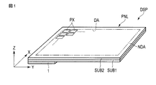
まず、本実施形態に係る表示装置について詳細に説明する。図1は、本実施形態に係る表示装置DSPの構成を概略的に示す斜視図である。図1は、第1方向Xと、第1方向Xに垂直な第2方向Yと、第1方向X及び第2方向Yに垂直な第3方向Zによって規定される三次元空間を示している。なお、第1方向X及び第2方向Yは、互いに直交しているが、90°以外の角度で交差していてもよい。また、本実施形態において、表示装置が液晶表示装置である場合について説明する。 First, the display device according to the present embodiment will be described in detail. FIG. 1 is a perspective view schematically showing the configuration of the display device DSP according to the present embodiment. FIG. 1 shows a three-dimensional space defined by a first direction X, a second direction Y perpendicular to the first direction X, and a third direction Z perpendicular to the first direction X and the second direction Y. . The first direction X and the second direction Y are orthogonal to each other, but may intersect at an angle other than 90°. Further, in the present embodiment, a case where the display device is a liquid crystal display device will be described.
図1に示すように、表示装置DSPは、アクティブマトリクス型の液晶表示パネルPNLと、配線基板1とを備えている。液晶表示パネルPNLは、平板状の第1基板SUB1と、第1基板SUB1に対向配置された平板状の第2基板SUB2と、第1基板SUB1と第2基板SUB2との間に挟持された液晶層(後述する液晶層LQ)と、を備えている。なお、本実施形態に係る液晶表示パネルPNLは、反射型の液晶表示パネルである。 As shown in FIG. 1, the display device DSP includes an active matrix type liquid crystal display panel PNL and a wiring board 1. The liquid crystal display panel PNL includes a flat plate-shaped first substrate SUB1, a flat plate-shaped second substrate SUB2 arranged to face the first substrate SUB1, and a liquid crystal sandwiched between the first substrate SUB1 and the second substrate SUB2. A layer (a liquid crystal layer LQ described later). The liquid crystal display panel PNL according to this embodiment is a reflective liquid crystal display panel.
本実施形態においては、第3方向Zの正の向き、あるいは、第1基板SUB1から第2基板SUB2に向かう方向を上又は上方と定義し、第3方向Zの負の向き、あるいは、第2基板SUB2から第1基板SUB1に向かう方向を下又は下方と定義する。 In the present embodiment, the positive direction in the third direction Z or the direction from the first substrate SUB1 to the second substrate SUB2 is defined as upward or upward, and the negative direction in the third direction Z or the second direction The direction from the substrate SUB2 to the first substrate SUB1 is defined as downward or downward.
液晶表示パネルPNLは、画像を表示する表示領域DAと、表示領域DAを囲む額縁状の非表示領域NDAと、を備えている。液晶表示パネルPNLは、表示領域DAにおいて、複数の画素PXを備えている。複数の画素PXは、第1方向X及び第2方向Yに並べられ、マトリクス状に設けられている。 The liquid crystal display panel PNL includes a display area DA for displaying an image and a frame-shaped non-display area NDA surrounding the display area DA. The liquid crystal display panel PNL includes a plurality of pixels PX in the display area DA. The plurality of pixels PX are arranged in the first direction X and the second direction Y and arranged in a matrix.
一例では、第1基板SUB1の第1方向Xに平行な側縁の長さは、第2基板SUB2の第1方向Xに平行な側縁の長さと略等しい。また、第1基板SUB1の第2方向Yに平行な側縁の長さは、第2基板SUB2の第2方向Yに平行な側縁の長さと略等しい。つまり、第1基板SUB1のX−Y平面に平行な面積は、第2基板SUB2のX−Y平面に平行な面積と略等しい。本実施形態において、第1基板SUB1の各側縁は、第3方向Zにおいて、第2基板SUB2の各側縁と揃っている。 In one example, the length of the side edge of the first substrate SUB1 parallel to the first direction X is substantially equal to the length of the side edge of the second substrate SUB2 parallel to the first direction X. The length of the side edge of the first substrate SUB1 parallel to the second direction Y is substantially equal to the length of the side edge of the second substrate SUB2 parallel to the second direction Y. That is, the area of the first substrate SUB1 parallel to the XY plane is substantially equal to the area of the second substrate SUB2 parallel to the XY plane. In the present embodiment, each side edge of the first substrate SUB1 is aligned with each side edge of the second substrate SUB2 in the third direction Z.
配線基板1は、液晶表示パネルPNLの下方に配置されている。一例では、配線基板1の第1方向Xに平行な側縁の長さは、第1基板SUB1及び第2基板SUB2の第1方向Xに平行な側縁の長さより短い、もしくは同等である。また、配線基板1の第2方向Yに平行な側縁の長さは、第1基板SUB1及び第2基板SUB2の第2方向Yに平行な側縁の長さより短い、もしくは同等である。配線基板1は、非表示領域NDA及び表示領域DAに位置している。本実施形態において、配線基板1の第1方向Xに平行な一側縁は、第3方向Zにおいて、液晶表示パネルPNLの一端と揃っている。なお、配線基板1は、液晶表示パネルPNLと対向する領域よりも外側にはみ出すことはない。液晶表示パネルPNL及び配線基板1は、互いに電気的に接続されている。 The wiring board 1 is arranged below the liquid crystal display panel PNL. In one example, the length of the side edge of the wiring board 1 parallel to the first direction X is shorter than or equal to the length of the side edge of the first substrate SUB1 and the second substrate SUB2 parallel to the first direction X. In addition, the length of the side edge of the wiring board 1 parallel to the second direction Y is shorter than or equal to the length of the side edge of the first substrate SUB1 and the second substrate SUB2 parallel to the second direction Y. The wiring board 1 is located in the non-display area NDA and the display area DA. In the present embodiment, one side edge of the wiring board 1 parallel to the first direction X is aligned with one end of the liquid crystal display panel PNL in the third direction Z. The wiring board 1 does not extend outside the region facing the liquid crystal display panel PNL. The liquid crystal display panel PNL and the wiring board 1 are electrically connected to each other.
図2は、図1に示した表示装置DSPの第1基板SUB1を示す概略平面図である。
図2に示すように、第1基板SUB1は、表示領域DAにおいて、第1方向Xに延出し第2方向Yに並んだ複数のゲート配線G、第2方向Yに延出し第1方向Xに並んだ複数のソース配線S、各画素PXにおいてゲート配線G及びソース配線Sと電気的に接続された薄膜トランジスタTr等を備えている。各画素PXは、例えば、隣り合う2本のゲート配線Gと隣り合う2本のソース配線Sとによって区画されている。薄膜トランジスタTrは、スイッチング素子として機能する。
FIG. 2 is a schematic plan view showing the first substrate SUB1 of the display device DSP shown in FIG.
As shown in FIG. 2, the first substrate SUB1 includes a plurality of gate lines G extending in the first direction X and arranged in the second direction Y, extending in the second direction Y, and extending in the second direction Y in the display area DA. A plurality of lined source lines S, a thin film transistor Tr electrically connected to the gate line G and the source line S in each pixel PX, and the like are provided. Each pixel PX is partitioned by, for example, two adjacent gate lines G and two adjacent source lines S. The thin film transistor Tr functions as a switching element.
非表示領域NDAに位置する第1基板SUB1の一端部SUB1eには、複数のパッド電極PDと、複数のコンタクトホールCHaと、が形成されている。パッド電極PDの各々は、コンタクトホールCHaと重なる位置に形成されている。各ソース配線S及びゲート配線Gは、非表示領域NDAに引き出され、それぞれパッド電極PDと電気的に接続されている。配線基板1の少なくとも一部は、図中に破線で示したように、第1基板SUB1の一端部SUB1eに重なって配置されている。配線基板1は、後述するように、コンタクトホールCHa内の図示されない導電材料を通じて、パッド電極PDと電気的に接続される。 A plurality of pad electrodes PD and a plurality of contact holes CHa are formed in the one end portion SUB1e of the first substrate SUB1 located in the non-display area NDA. Each pad electrode PD is formed at a position overlapping the contact hole CHa. The source lines S and the gate lines G are drawn out to the non-display area NDA and electrically connected to the pad electrodes PD. At least a part of the wiring board 1 is arranged so as to overlap the one end portion SUB1e of the first substrate SUB1 as shown by a broken line in the drawing. The wiring board 1 is electrically connected to the pad electrode PD through a conductive material (not shown) in the contact hole CHa, as described later.
図3は、図1に示した表示装置DSPの表示領域DAを示す断面図である。なお、図3は、一例として、Twisted Nematic(TN)モードを用いた反射型の液晶表示装置を示している。 FIG. 3 is a cross-sectional view showing the display area DA of the display device DSP shown in FIG. Note that FIG. 3 illustrates, as an example, a reflective liquid crystal display device using the Twisted Nematic (TN) mode.
図3に示すように、第1基板SUB1は、支持基板5、遮光マスク(遮光体)LS、第1絶縁基板10、薄膜トランジスタTr、反射層4、画素電極PE、第1配向膜AL1等を備えている。支持基板5は、例えば、ガラス基板である。遮光マスクLSは、支持基板5の上に配置されている。遮光マスクLSは、レーザー光を遮蔽する。本実施形態において、遮光マスクLSは、レーザー光を反射する材料を用いて形成され、例えば、エキシマレーザー光を反射する材料で形成されている。第1絶縁基板10は、支持基板5及び遮光マスクLSの上方に配置されている。すなわち、遮光マスクLSは、支持基板5と第1絶縁基板10との間に位置している。第1絶縁基板10は、有機絶縁材料を用いて形成され、例えばポリイミドを用いて形成される。第1絶縁基板10は、第1絶縁膜11によって覆われている。
As shown in FIG. 3, the first substrate SUB1 includes a
薄膜トランジスタTrは、第1絶縁膜11の上方に形成されている。図示した例では、薄膜トランジスタTrはトップゲート型に構成されているが、ボトムゲート型であっても良い。薄膜トランジスタTrは、第1絶縁膜11の上に形成された半導体層SCを備えている。半導体層SCは、第2絶縁膜12によって覆われている。また、第2絶縁膜12は、第1絶縁膜11の上にも配置されている。
The thin film transistor Tr is formed above the first insulating
薄膜トランジスタTrのゲート電極WGは、第2絶縁膜12の上に形成され、半導体層SCの直上に位置している。ゲート電極WGは、ゲート配線Gに電気的に接続され(あるいは、ゲート配線Gと一体的に形成され)、第3絶縁膜13によって覆われている。また、第3絶縁膜13は、第2絶縁膜12の上にも配置されている。
The gate electrode WG of the thin film transistor Tr is formed on the second insulating
このような第1絶縁膜11、第2絶縁膜12、及び、第3絶縁膜13は、例えば、シリコン酸化物やシリコン窒化物等の無機系材料によって形成されている。
The first insulating
薄膜トランジスタTrのソース電極WS及びドレイン電極WDは、第3絶縁膜13の上に形成されている。また、ソース配線Sも同様に第3絶縁膜13の上に形成されている。ソース電極WSは、ソース配線Sに電気的に接続されている(あるいは、ソース配線Sと一体的に形成されている)。ソース電極WS及びドレイン電極WDは、それぞれ第2絶縁膜12及び第3絶縁膜13を貫通するコンタクトホールCH1、CH2を通して半導体層SCと電気的に接続されている。薄膜トランジスタTrは、第4絶縁膜14によって覆われている。第4絶縁膜14は、第3絶縁膜13の上にも配置されている。このような第4絶縁膜14は、例えば、透明な樹脂等の有機系材料によって形成されている。
The source electrode WS and the drain electrode WD of the thin film transistor Tr are formed on the third insulating
反射層4は、例えば、第4絶縁膜14の上に形成されている。反射層4は、アルミニウムや銀等の反射率が高い金属材料で形成される。なお、反射層4の表面(つまり、第2基板SUB2側の面)は、光散乱性を付与するための凹凸面であることが望ましい。
The
画素電極PEは、第4絶縁膜14の上に形成されるが、図示した例では、反射層4に重なっている。なお、反射層4は、画素電極PEと対向する位置に形成されていれば良く、画素電極PEと反射層4との間に他の絶縁膜が介在していても良い。画素電極PEは、第4絶縁膜14を貫通するコンタクトホールCH3を通して薄膜トランジスタTrのドレイン電極WDにコンタクトしている。画素電極PEは、例えば、インジウム・ティン・オキサイド(ITO)やインジウム・ジンク・オキサイド(IZO)等の透明な導電材料によって形成されている。画素電極PEは、第1配向膜AL1によって覆われている。
Although the pixel electrode PE is formed on the fourth insulating
一方、第2基板SUB2は、第1基板SUB1の上方に位置し、第1基板SUB1に対向配置されている。第2基板SUB2は、第2絶縁基板30、遮光層BM、カラーフィルタCF、オーバーコート層OC、共通電極CE、第2配向膜AL2等を備えている。第2絶縁基板30は、ガラス基板や樹脂基板等の光透過性を有する材料を用いて形成されている。
On the other hand, the second substrate SUB2 is located above the first substrate SUB1 and is arranged to face the first substrate SUB1. The second substrate SUB2 includes a second insulating
遮光層BMは、第2絶縁基板30の第1基板SUB1に対向する側に形成されている。遮光層BMは、各画素PXを区画するように形成されており、第1基板SUB1に設けられたゲート配線Gやソース配線S、さらには薄膜トランジスタTr等の配線部やコンタクトホールCH3等に対向するように形成されている。遮光層BMは、遮光性の金属材料や黒色の樹脂材料によって形成されている。
The light shielding layer BM is formed on the side of the second insulating
カラーフィルタCFは、第2絶縁基板30の第1基板SUB1に対向する側に形成され、その一部が遮光層BMに重なっている。カラーフィルタCFは、互いに異なる複数の色、例えば赤色、青色、緑色にそれぞれ着色された樹脂材料によって形成されている。赤色のカラーフィルタは赤色画素に対応して配置され、緑色のカラーフィルタは緑色画素に対応して配置され、青色のカラーフィルタは青色画素に対応して配置されている。なお、カラーフィルタCFは、さらに、白色あるいは透明のカラーフィルタを含んでいても良い。異なる色のカラーフィルタCF間の境界は、遮光層BMと対向している。
The color filter CF is formed on the side of the second insulating
オーバーコート層OCは、カラーフィルタCFを覆っている。オーバーコート層OCは、透明な樹脂材料によって形成されている。 The overcoat layer OC covers the color filter CF. The overcoat layer OC is formed of a transparent resin material.
共通電極CEは、オーバーコート層OCの第1基板SUB1と対向する側に形成されている。このような共通電極CEは、例えば、ITOやIZO等の透明な導電材料によって形成されている。共通電極CEは、第2配向膜AL2によって覆われている。 The common electrode CE is formed on the side of the overcoat layer OC facing the first substrate SUB1. Such a common electrode CE is made of, for example, a transparent conductive material such as ITO or IZO. The common electrode CE is covered with the second alignment film AL2.
上述したような第1基板SUB1と第2基板SUB2において、第1配向膜AL1及び第2配向膜AL2は、互いに対向して配置されている。このとき、第1基板SUB1と第2基板SUB2の間には、図示しないスペーサにより、所定のセルギャップが形成される。第1基板SUB1と第2基板SUB2とは、セルギャップが形成された状態で図示しないシール材によって貼り合わせられている。液晶層LQは第1配向膜AL1と第2配向膜AL2の間に封入されている。第2絶縁基板30の外面30Bには、偏光板PLを含む光学素子ODが配置されている。このような光学素子ODは、表示面側に位置している。
In the first substrate SUB1 and the second substrate SUB2 as described above, the first alignment film AL1 and the second alignment film AL2 are arranged to face each other. At this time, a predetermined cell gap is formed between the first substrate SUB1 and the second substrate SUB2 by a spacer (not shown). The first substrate SUB1 and the second substrate SUB2 are attached to each other with a sealing material (not shown) in the state where the cell gap is formed. The liquid crystal layer LQ is enclosed between the first alignment film AL1 and the second alignment film AL2. An optical element OD including a polarizing plate PL is arranged on the
図4は、図1に示した表示装置DSPの非表示領域NDAを含んだ断面図である。なお、ここでは、第2基板SUB2は、図3に示した第2基板SUB2の構造と略同一であるため、その詳細な構造についての説明は省略する。また、本実施形態においては、第2基板SUB2から第1基板SUB1を見ることを平面視と定義する。 FIG. 4 is a cross-sectional view including the non-display area NDA of the display device DSP shown in FIG. Since the second substrate SUB2 has substantially the same structure as the second substrate SUB2 shown in FIG. 3, a detailed description of the structure will be omitted. Further, in the present embodiment, viewing the first substrate SUB1 from the second substrate SUB2 is defined as a plan view.
図4に示すように、第1基板SUB1及び第2基板SUB2は、シール材SLによって貼り合わせられている。液晶層LQは、第1基板SUB1及び第2基板SUB2と、シール材SLによって囲まれた領域内に備えられている。シール材SLは、非表示領域NDAに形成されている。 As shown in FIG. 4, the first substrate SUB1 and the second substrate SUB2 are bonded together by a seal material SL. The liquid crystal layer LQ is provided in a region surrounded by the first substrate SUB1 and the second substrate SUB2 and the sealing material SL. The seal material SL is formed in the non-display area NDA.
支持基板5及び遮光マスクLSは、非表示領域NDAにおいて、第1基板SUB1の端部まで延在しておらず途切れている。つまり、支持基板5及び遮光マスクLSは、図2に示したような、第1基板SUB1の一端部SUB1e側の側縁まで延在して形成されていない。ここで、第1基板SUB1は、第1領域AR1及び第2領域AR2を有している。第1領域AR1は、平面視で、支持基板5及び遮光マスクLSが配置されている領域に相当し、第2領域AR2は、平面視で、支持基板5及び遮光マスクLSが配置されていない領域に相当する。支持基板5及び遮光マスクLSは、平面視で、シール材SLの一部と重なっている。シール材SLは、第1領域AR1と第2領域AR2との境界を跨いで形成されている。
In the non-display area NDA, the
第1絶縁基板10は、第1領域AR1において厚さW1を有しており、第2領域AR2において厚さW2を有している。厚さW2は、厚さW1よりも小さい。本実施形態においては、例えば、厚さW1は約10μmであり、厚さW2は、0μmより大きく、1μm以下である。
The first insulating
パッド電極PDは、第1絶縁基板10の上方に形成されている。図示した例では、パッド電極PDと第1絶縁基板10の層間に、第1絶縁膜11と、第2絶縁膜12と、第3絶縁膜13と、が配置されている。ここで、第1絶縁基板10とパッド電極PDとの間に配置される絶縁膜を絶縁膜ILとする。図示した例では、第1絶縁膜11、第2絶縁膜12、及び第3絶縁膜13は、絶縁膜ILに相当する。また、図示した例では、パッド電極PDは、電極P1及びP2が積層されることによって構成されている。電極P1は、例えば、透明導電材料としてのITOを用いて形成される。電極P2は、例えば、金属材料等の導電材料を用いて形成される。電極P2は、例えば、島状に形成されている。第1絶縁基板10及び絶縁膜ILには、パッド電極PDまで貫通するコンタクトホールCHaが形成されている。パッド電極PDは、コンタクトホールCHaと対向する位置に形成されている。パッド電極PD及びコンタクトホールCHaは、平面視で、第1基板SUB1の第2領域AR2に形成されている。また、コンタクトホールCHaは、平面視で、シール材SLと重なる位置に形成されている。なお、本実施形態においては、コンタクトホールCHaは、第1絶縁基板10及び絶縁膜ILを、パッド電極PDまで貫通する貫通部に相当する。
The pad electrode PD is formed above the first insulating
信号配線6は、図示した例では、第3絶縁膜13の上に形成され、パッド電極PDと同層に形成されている。信号配線6は、パッド電極PDと電気的に接続されている。信号配線6及びパッド電極PDは、それぞれ別々に形成されていても良いし、一体的に形成されていても良い。図示した例では、信号配線6は、パッド電極PDの電極P2と一体的に形成されている。信号配線6は、図2に示したゲート配線Gやソース配線S、電源線や各種制御用配線等に相当する。第4絶縁膜14は、信号配線6、パッド電極PD、第3絶縁膜13を覆っている。
In the illustrated example, the
なお、図示した例では、信号配線6及びパッド電極PDは、ソース配線Sと同層に配置されているが、他の層に配置されていても良い。また、信号配線6及びパッド電極PDが互いに異なる層に配置され、信号配線6及びパッド電極PDの間の層間絶縁膜に形成されたコンタクトホールを介して両者が電気的に接続されていても良い。
In the illustrated example, the
配線基板1は、コア基板200と、コア基板200の液晶表示パネルPNLと対向する側の面に配置された接続配線100と、コア基板200の液晶表示パネルPNLと対向する側の面とは反対側の面に配置された駆動部2と、を備えている。
The wiring board 1 is opposite to the
駆動部2は、コア基板200に形成されたスルーホール110を介して接続配線100と電気的に接続されている。駆動部2は、液晶表示パネルPNLを駆動するのに必要な信号を供給する信号供給源等として機能する。なお、駆動部2の位置は、特に制限されるものではなく、コア基板200の液晶表示パネルPNLと対向する側の面に配置されていても良い。
The
液晶表示パネルPNL及び配線基板1は、導電材料である異方性導電膜3を介して互いに電気的に接続されると共に接着されている。すなわち、異方性導電膜3は、接着剤中に分散された導電粒子(後述する導電粒子CP)を含んでいる。このため、配線基板1と液晶表示パネルPNLとの間に異方性導電膜3を介在させた状態で、配線基板1及び液晶表示パネルPNLを第3方向Zに上下から加圧し、加熱することによって、両者が電気的及び物理的に接続される。異方性導電膜3は、液晶表示パネルPNLと配線基板1との間で、第1絶縁基板10の下面からコンタクトホールCHaの内部に亘って充填され、パッド電極PDと接し、電気的に接続されている。また、異方性導電膜3は、接続配線100と接し、電気的に接続されている。これにより、接続配線100は、異方性導電膜3を介して、パッド電極PD及び信号配線6と電気的に接続されている。なお、本実施形態において、接続配線100の異方性導電膜3に接する側の面は、平坦である。
The liquid crystal display panel PNL and the wiring board 1 are electrically connected and bonded to each other via an anisotropic
また、シール材SLは、平面視で、コンタクトホールCHaと重なる位置に形成されている。このため、上記のように位置するシール材SLは、配線基板1と液晶表示パネルPNLとの良好な接続に寄与することができる。 Further, the sealing material SL is formed at a position overlapping the contact hole CHa in plan view. Therefore, the sealing material SL positioned as described above can contribute to a good connection between the wiring board 1 and the liquid crystal display panel PNL.
図5は、図4に示した表示装置DSPの一部を拡大して示す断面図であり、配線基板1、異方性導電膜3、第1絶縁基板10、絶縁膜IL、及びパッド電極PDの構成を示す図である。
図5に示すように、異方性導電膜3に含まれる導電粒子CP1は、コンタクトホールCHaにおいて、パッド電極PDと接続配線100との間に介在している。配線基板1が液晶表示パネルPNLに圧着される際に、導電粒子CP1が接続配線100とパッド電極PDとの間で押しつぶされ、両者を電気的に接続することができる。このとき、接続配線100とパッド電極PDとの間の高さhは、導電粒子CP1を十分に押しつぶす程に小さくなる。また、図示した例では、第2領域AR2のうち、異方性導電膜3に含まれる導電粒子CP2は、コンタクトホールCHaの外側において、第1絶縁基板10と接続配線100との間に介在している。このとき、導電粒子CP2は、第1絶縁基板10と接続配線100との間に噛みこんでいても良い。本実施形態において、導電粒子CP2が噛みこむとは、配線基板1と液晶表示パネルPNLとが圧着される際に、導電粒子CP2にかかる圧力に対して、導電粒子CP2がそれ以上押しつぶされない状態を指す。導電粒子CP1及びCP2は、例えば、全体が金属製であってもよく、樹脂材料をニッケルや金等の金属材料でコーティングしたものであっても良い。
FIG. 5 is an enlarged cross-sectional view showing a part of the display device DSP shown in FIG. 4. The wiring substrate 1, the anisotropic
As shown in FIG. 5, the conductive particles CP1 included in the anisotropic
なお、導電粒子CPは、配線基板1と液晶表示パネルPNLとの間において、第3方向Zに2個以上が重なって導通することはない。また、例えば、第1方向X及び第2方向Yについては、隣り合う導電粒子CPの間に異方性導電膜3を形成する接着剤(絶縁体)が入り込むため、導電粒子CP同士が第1方向X及び第2方向Yで互いに導通することはほとんどない。
It should be noted that, between the wiring substrate 1 and the liquid crystal display panel PNL, two or more conductive particles CP do not overlap each other in the third direction Z and become conductive. Further, for example, in the first direction X and the second direction Y, the adhesive (insulator) that forms the anisotropic
本実施形態によれば、第2領域AR2における第1絶縁基板10は、第1領域AR1における第1絶縁基板10より薄い。このため、導電粒子CP2が、接続配線100と第1絶縁基板10との間に介在し押しつぶされていても、コンタクトホールCH1aと対向する位置でのパッド電極PDと接続配線100との間の高さhは、導電粒子CP1を十分に押しつぶす程に小さくなる。つまり、接続配線100とパッド電極PDとの間の導電粒子CP1は、導電粒子CP2が接続配線100と第1絶縁基板10との間に噛みこむ以前に押しつぶされる。したがって、接続配線100とパッド電極PDの接続の歩留りを向上することが可能となる。
According to the present embodiment, the first insulating
また、本実施形態によれば、表示装置DSPにおいて、配線基板1が、液晶表示パネルPNLの下方(表示面とは反対の背面側)に配置され、配線基板1及び液晶表示パネルPNLは、コンタクトホールCHa内の導電材料(上記の例では異方性導電膜3)を介して電気的に接続されている。また、駆動部2は、液晶表示パネルPNLの下方に配置されている。そのため、駆動部2や配線基板1を配置するために、第1基板SUB1の実装部の面積を拡大する必要がなく、第1基板SUB1と第2基板SUB2とを略同等の面積で形成することが可能となる。また、第1基板SUB1と第2基板SUB2とが対向する領域内で、アクティブエリアACTを拡大することが可能となる。つまり、本実施形態の表示装置DSPの表示面において、アクティブエリアACTに寄与する面積の割合が向上し、狭額縁化することが可能である。
Further, according to the present embodiment, in the display device DSP, the wiring board 1 is arranged below the liquid crystal display panel PNL (on the back side opposite to the display surface), and the wiring board 1 and the liquid crystal display panel PNL are in contact with each other. The holes CHa are electrically connected through the conductive material (anisotropic
また、第1基板SUB1の第2基板SUB2と対向する側から配線基板1までを電気的に接続するための長尺のフレキシブル・プリント回路基板が不要であり、折り曲げたフレキシブル・プリント回路基板を収容するためのスペースも不要となる。このため、表示装置DSPを小型化することが可能となる。さらには、表示装置DSPを組み込んだ電子機器を小型化することも可能となる。
さらに、フレキシブル・プリント回路基板を折り曲げて収容した際の配線の断線を回避することができるため、表示装置DSPの信頼性を向上することが可能となる。
In addition, a long flexible printed circuit board for electrically connecting the side of the first substrate SUB1 facing the second substrate SUB2 to the wiring board 1 is unnecessary, and the folded flexible printed circuit board is accommodated. There is no need for a space to do so. Therefore, the display device DSP can be downsized. Further, it is possible to downsize an electronic device incorporating the display device DSP.
Furthermore, since it is possible to avoid disconnection of the wiring when the flexible printed circuit board is folded and housed, it is possible to improve the reliability of the display device DSP.
さらに、コンタクトホールCHaは、シール材SLと対向する位置に形成される。シール材SLは、ファイバー等の固形物を含んでいるため、シール材SLが介在する額縁領域PRPにおいては、アクティブエリアACTと比較して、液晶表示パネルPNLの第3方向Zにかかる力に対して強度を向上することができる。つまり、配線基板1を液晶表示パネルPNLに圧着する際に、第3方向Zにかかる力による液晶表示パネルPNLの破損を抑制することが可能である。 Further, the contact hole CHa is formed at a position facing the sealing material SL. Since the sealing material SL contains solid matter such as fibers, in the frame region PRP in which the sealing material SL is interposed, as compared with the active area ACT, with respect to the force applied in the third direction Z of the liquid crystal display panel PNL. Strength can be improved. That is, it is possible to suppress damage to the liquid crystal display panel PNL due to the force applied in the third direction Z when the wiring board 1 is pressure-bonded to the liquid crystal display panel PNL.
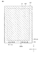
図6は、上記実施形態に係る第1基板SUB1を示す平面図であり、第1領域AR1及び第2領域AR2の位置関係等を示す図である。
図6において、第1領域AR1は、斜線で示されている。支持基板5及び遮光マスクLSは、第1領域AR1の全面に亘って配置されている。第2領域AR2は、第1領域AR1に隣接し、第1基板SUB1の一端部SUB1e側の非表示領域NDAにおいて、第1方向Xに延出している。複数のパッド電極PD及びコンタクトホールCHaは、第2領域AR2において、第1方向Xに並んで配置されている。
FIG. 6 is a plan view showing the first substrate SUB1 according to the above embodiment, and is a view showing the positional relationship between the first area AR1 and the second area AR2.
In FIG. 6, the first area AR1 is indicated by diagonal lines. The
なお、図4に示したような第1絶縁基板10は、液晶表示パネルPNLの全面に亘って配置されている。また、上述したように、厚さW2は、厚さW1より小さい。すなわち、パッド電極PD及びコンタクトホールCHaは、上記第1絶縁基板10のうち厚みの小さい領域に位置している。
The first insulating
次に、本実施形態の表示装置DSPの製造工程について、図7から図10を用いて説明する。図7乃至図10は、本実施形態の配線基板1の液晶表示パネルPNLへの圧着方法を説明するための概略断面図である。図7乃至図10に示されるパッド電極PDより上層の構造は、図4に示した液晶表示パネルPNLにおける、パッド電極PDより上層の構造と等しい。 Next, a manufacturing process of the display device DSP according to the present embodiment will be described with reference to FIGS. 7 to 10 are schematic cross-sectional views for explaining a method of crimping the wiring board 1 of the present embodiment to the liquid crystal display panel PNL. The structure above the pad electrode PD shown in FIGS. 7 to 10 is the same as the structure above the pad electrode PD in the liquid crystal display panel PNL shown in FIG.
図7は、上記実施形態に係る第1基板SUB1と第2基板SUB2とを貼り合わせる第1の工程を説明するための断面図である。
図7に示すように、まず、支持基板5上に遮光マスクLSが形成される。遮光マスクLSは、第1基板SUB1の第1領域AR1に形成される。支持基板5及び遮光マスクLS上に有機絶縁膜を成膜することによって第1絶縁基板10が形成される。その後、第1絶縁膜11、第2絶縁膜12、第3絶縁膜13、パッド電極PD、信号配線6、第4絶縁膜14、第1配向膜AL1等を順次形成して、第1基板SUB1が形成される。一方で、第2基板SUB2が形成される。
FIG. 7 is a cross-sectional view for explaining the first step of bonding the first substrate SUB1 and the second substrate SUB2 according to the above embodiment.
As shown in FIG. 7, first, the light shielding mask LS is formed on the
その後、第1基板SUB1又は第2基板SUB2にシール材SLを形成し、シール材SLによって囲まれた内側に液晶材料を滴下した後に、第1基板SUB1と第2基板SUB2とを貼り合わせる。 After that, the sealing material SL is formed on the first substrate SUB1 or the second substrate SUB2, the liquid crystal material is dropped inside the area surrounded by the sealing material SL, and then the first substrate SUB1 and the second substrate SUB2 are bonded together.
次に、第1絶縁基板10から支持基板5を部分的に剥離するために、支持基板5の背面側からレーザー光LLを照射する。ここで、本実施形態においては、例えば、支持基板5はガラスによって形成され、第1絶縁基板10はポリイミドによって形成されている。支持基板5の背面側からレーザー光LLが照射されると、第2領域AR2において、レーザー光LLは、第1絶縁基板10の面10Aに到達する。第1絶縁基板10は、支持基板5と第1絶縁基板10との間の界面で、レーザー光LLを吸収して分解する。これにより、支持基板5及び第1絶縁基板10の界面に空間が生じる。この時、第1領域AR1においては、遮光マスクLSが配置されており、レーザー光LLが第1絶縁基板10の面10Aに到達しないため、第1絶縁基板10と遮光マスクLSとの界面は剥離しない。
Next, in order to partially peel the supporting
図8は、図7の第1の工程に続く、支持基板5を第1絶縁基板10から部分的に剥離し、第1絶縁基板10に第1コンタクトホールCHa1を形成する第2の工程を説明するための断面図である。
図8に示すように、レーザー光が照射された後、第1領域AR1においては、支持基板5は、遮光マスクLSを介して第1絶縁基板10に固定されているが、第2領域AR2においては、支持基板5は、第1絶縁基板10から浮いた状態である。その後、第1領域AR1及び第2領域AR2の境界で支持基板5を切断することにより、第2領域AR2において支持基板5が取り除かれる。なお、支持基板5を切断する位置は、遮光マスクLSの端と対向する位置に限定されるものではない。例えば、支持基板5を切断する位置は、遮光マスクLSの端から距離を置いた位置であって、遮光マスクLSと対向しない位置であってもよい。
FIG. 8 illustrates a second step following the first step of FIG. 7 in which the
As shown in FIG. 8, after being irradiated with the laser light, the
第2領域AR2において、支持基板5が第1絶縁基板10から剥離された後、第1絶縁基板10に第1コンタクトホールCHa1を形成する工程が行われる。すなわち、第1基板SUB1の下方側から、シール材SLと重なる領域に向けてレーザー光が照射されることによって、第1絶縁基板10に絶縁膜ILまで貫通した第1コンタクトホールCHa1が形成される。本実施形態においては、例えば、258nm以下の波長域を有するレーザー光を用いるのが好ましい。第1コンタクトホールCHa1は、第1貫通部として機能している。
After the
図9は、図8の第2の工程に続く、第2領域AR2において第1絶縁基板10を薄膜化しつつ、絶縁膜ILに第2コンタクトホールCHa2を形成する第3の工程を説明するための断面図である。
次いで、絶縁膜ILに第2コンタクトホールCHa2を形成する工程が行われる。絶縁膜ILが第1コンタクトホールCHa1の内部でアッシング処理によって削られることにより、第2コンタクトホールCHa2が形成される。第2コンタクトホールCHa2は、第1コンタクトホールCHa1に重なる位置に形成されている。第2コンタクトホールCHa2は、第1コンタクトホールCHa1につながっている。第2コンタクトホールCHa2は、第2貫通部として機能している。すなわち、コンタクトホールCHaは、第1絶縁基板10に形成された第1コンタクトホールCHa1と絶縁膜ILに形成された第2コンタクトホールCHa2とによって構成されている。アッシング処理に用いられるガスとしては、例えば、六フッ化硫黄(SF6)が用いられる。
FIG. 9 is a view for explaining a third step following the second step of FIG. 8 for forming the second contact hole CHa2 in the insulating film IL while thinning the first insulating
Next, a step of forming the second contact hole CHa2 in the insulating film IL is performed. The second contact hole CHa2 is formed by shaving the insulating film IL inside the first contact hole CHa1 by an ashing process. The second contact hole CHa2 is formed at a position overlapping the first contact hole CHa1. The second contact hole CHa2 is connected to the first contact hole CHa1. The second contact hole CHa2 functions as a second penetrating portion. That is, the contact hole CHa is composed of the first contact hole CHa1 formed in the first insulating
また、第2コンタクトホールCHa2が形成される工程と同一工程で、第2領域AR2において第1絶縁基板10が薄膜化される。つまり、第2コンタクトホールCHa2を形成するためのアッシング処理により、第2領域AR2において露出した第1絶縁基板10も削られる。第1絶縁基板10は、第1領域AR1においては、支持基板5及び遮光マスクLSによって覆われているため削られない。そのため、第1領域AR1における第1絶縁基板10の厚さW1より、第2領域AR2における第2絶縁基板10の厚さW2が小さくなる。
In addition, in the same step as the step of forming the second contact hole CHa2, the first insulating
ここで、絶縁膜ILがアッシング処理のガスに対して反応する速度と、第1絶縁基板10がアッシング処理のガスに対して反応する速度は異なっている。また、例えば、絶縁膜ILと第1絶縁基板10とでは、第1絶縁基板10の方がアッシング処理による削れ始めの時間が遅い。そのため、絶縁膜IL及び第1絶縁基板10のそれぞれのアッシング処理に対する反応速度を考慮し、両者のアッシング処理前の膜厚を設定することにより、第2領域AR2において、絶縁膜ILがパッド電極PDまで貫通して削られる時間に、第1絶縁基板10を所望の厚さW2まで削ることが可能となる。
Here, the speed at which the insulating film IL reacts with the ashing gas and the speed at which the first insulating
本実施形態では、上記のように、絶縁膜ILの第2コンタクトホールCHa2を形成する工程と、第1絶縁基板10の薄膜化の工程が同時に行われる。これにより、レーザー光による第1絶縁基板10の薄膜化の工程を必要とせず、製造工程を増やさずに第1絶縁基板10を薄膜化することが可能である。また、これにより製造コストを抑制することができる。
In the present embodiment, as described above, the step of forming the second contact hole CHa2 of the insulating film IL and the step of thinning the first insulating
図10は、図9の第3の工程に続く、配線基板1を液晶表示パネルPNLに圧着する第4の工程を説明するための断面図である。
図10に示すように、第1基板SUB1に、コンタクトホールCHaが形成された後、異方性導電膜3を用いて、配線基板1を液晶表示パネルPNLに圧着する工程が行われる。すなわち、配線基板1と液晶表示パネルPNLとの間であってコンタクトホールCHaと対向する位置に、異方性導電膜3を配置し、配線基板1の下方及び液晶表示パネルPNLの上方から、図9に示した矢印の方向に圧力を加え加熱する。これにより、異方性導電膜3が溶融してコンタクトホールCHa内に浸潤するとともに、異方性導電膜3に含まれる導電粒子がパッド電極PDに接触し、配線基板1及び液晶表示パネルPNLが電気的及び物理的に接続される。
以上の工程により、配線基板1が液晶表示パネルPNLに圧着される。
以上説明したように、本実施形態によれば、小型化及び狭額縁化が可能な表示装置を得ることができる。
FIG. 10 is a cross-sectional view for explaining a fourth step of crimping the wiring substrate 1 to the liquid crystal display panel PNL, which is subsequent to the third step of FIG.
As shown in FIG. 10, after the contact hole CHa is formed in the first substrate SUB1, a process of pressure-bonding the wiring substrate 1 to the liquid crystal display panel PNL is performed using the anisotropic
Through the above steps, the wiring board 1 is pressure bonded to the liquid crystal display panel PNL.
As described above, according to this embodiment, it is possible to obtain a display device that can be downsized and have a narrow frame.
次に、上記実施形態の変形例1について説明する。
図11は、上記実施形態に係る表示装置DSPの変形例1の一部を拡大して示す断面図であり、配線基板1、異方性導電膜3、第1絶縁基板10、絶縁膜IL、及びパッド電極PDの構成を示す図である。図11に示した構成は、図5と比較して、接続配線100が、凸部Tを有している点で相違している。
Next, a first modification of the above embodiment will be described.
FIG. 11 is a cross-sectional view showing a part of Modification 1 of the display device DSP according to the above embodiment in an enlarged manner. The wiring substrate 1, the anisotropic
接続配線100は、凸部Tを有している。接続配線100の凸部Tは、コンタクトホールCHaと平面視で重なる位置に形成されている。凸部Tは、第1基板SUB1側に突出している。凸部Tは、少なくとも一部がコンタクトホールCHa内に設けられている。凸部Tは、例えば、接続配線100の上にメッキ等の手法を用いて形成される。
The
導電粒子CP1は、コンタクトホールCHaにおいて、パッド電極PD及び凸部Tとの間に介在している。上記のように、接続配線100が凸部Tを有することにより、コンタクトホールCH11において、接続配線100の凸部Tがパッド電極PDとの間に設けられているより多くの数の導電粒子CP1を押しつぶすことが可能となる。このため、小さい圧着力で、接続配線100とパッド電極PDとをより確実に電気的に接続することができる。したがって、製品歩留まり、製造歩留まり及び信頼性を向上することが可能となる。
このような変形例1においても、上記した実施形態と同様の効果が得られる。
The conductive particles CP1 are interposed between the pad electrode PD and the protrusion T in the contact hole CHa. As described above, since the
Also in such a modified example 1, the same effect as that of the above-described embodiment can be obtained.
図12は、上記実施形態に係る表示装置DSPの変形例2を示す断面図である。図12に示した例では、表示装置として、有機エレクトロルミネッセンス(EL)表示装置を示している。
まず、表示素子部120における表示装置の構造を説明する。なお、上記の構成例と同一の構成については同一の参照符号を付して詳細な説明を省略する。
FIG. 12 is a cross-sectional view showing Modification Example 2 of the display device DSP according to the above embodiment. In the example shown in FIG. 12, an organic electroluminescence (EL) display device is shown as the display device.
First, the structure of the display device in the
図12に示すように、第1基板SUB1は、支持基板5、遮光マスクLS、第1絶縁基板10、スイッチング素子SW1、SW2、SW3、有機EL素子OLED1、OLED2、OLED3等を備えている。遮光マスクLSは、支持基板5及び第1絶縁基板10との間に位置している。スイッチング素子SW1乃至SW3は、第1絶縁膜11の上に形成されている。反射層4は、第4絶縁膜14の上に形成されている。
As shown in FIG. 12, the first substrate SUB1 includes a
有機EL素子OLED1乃至OLED3は、第4絶縁膜14の上に形成されている。図示した例では、有機EL素子OLED1はスイッチング素子SW1と電気的に接続され、有機EL素子OLED2はスイッチング素子SW2と電気的に接続され、有機EL素子OLED3はスイッチング素子SW3と電気的に接続されている。有機EL素子OLED1乃至OLED3は、いずれも第2基板SUB2の側に向かって白色光を放射するトップエミッションタイプとして構成されている。このような有機EL素子OLED1乃至OLED3は、いずれも同一構造である。
The organic EL elements OLED1 to OLED3 are formed on the fourth insulating
有機EL素子OLED1は、反射層4の上に形成された陽極PE1を備えている。陽極PE1は、スイッチング素子SW1のドレイン電極WDとコンタクトし、スイッチング素子SW1と電気的に接続されている。同様に、有機EL素子OLED2はスイッチング素子SW2と電気的に接続された陽極PE2を備え、有機EL素子OLED3はスイッチング素子SW3と電気的に接続された陽極PE3を備えている。
The organic EL element OLED1 includes an anode PE1 formed on the
有機EL素子OLED1乃至OLED3は、さらに、有機発光層ORG及び共通電極(陰極)CEを備えている。有機発光層ORGは、陽極PE1乃至PE3の上にそれぞれ位置している。共通電極CEは、有機発光層ORGの上に位置している。図示した例では、有機EL素子OLED1乃至OLED3は、それぞれリブ15によって区画されている。なお、図示しないが、有機EL素子OLED1乃至OLED3は、透明な封止膜によって封止されていることが望ましい。
表示素子部120とは、第1基板SUB1のうち、複数のスイッチング素子及び有機EL素子OLEDが並んだ領域に相当し、実質的に画像を表示する表示領域である。
The organic EL elements OLED1 to OLED3 further include an organic light emitting layer ORG and a common electrode (cathode) CE. The organic light emitting layer ORG is located on each of the anodes PE1 to PE3. The common electrode CE is located on the organic light emitting layer ORG. In the illustrated example, the organic EL elements OLED1 to OLED3 are partitioned by the
The
第2基板SUB2は、第2絶縁基板30の内面30A側に、カラーフィルタ層220等を備えている。カラーフィルタ層220は、カラーフィルタCF1、カラーフィルタCF2、及び、カラーフィルタCF3を備えている。カラーフィルタCF1は、有機EL素子OLED1と対向し、白色のうちの青色波長の光を透過する青色カラーフィルタである。カラーフィルタCF2は、有機EL素子OLED2と対向し、白色のうちの緑色波長の光を透過する緑色カラーフィルタである。カラーフィルタCF3は、有機EL素子OLED3と対向し、白色のうちの赤色波長の光を透過する赤色カラーフィルタである。
このような第1基板SUB1の表示素子部120と第2基板SUB2とは、透明な接着剤41によって接着されている。
The second substrate SUB2 includes a
The
このような表示装置においては、有機EL素子OLED1乃至OLED3のそれぞれが発光した際、それぞれの放射光(白色光)は、カラーフィルタCF1、カラーフィルタCF2、カラーフィルタCF3を介してそれぞれ外部に出射される。このとき、有機EL素子OLED1から放射された白色光のうち、青色波長の光がカラーフィルタCF1を透過する。また、有機EL素子OLED2から放射された白色光のうち、緑色波長の光がカラーフィルタCF2を透過する。また、有機EL素子OLED3から放射された白色光のうち、赤色波長の光がカラーフィルタCF3を透過する。これにより、カラー表示が実現される。 In such a display device, when each of the organic EL elements OLED1 to OLED3 emits light, each emitted light (white light) is emitted to the outside via the color filter CF1, the color filter CF2, and the color filter CF3. It At this time, of the white light emitted from the organic EL element OLED1, light of a blue wavelength passes through the color filter CF1. Further, of the white light emitted from the organic EL element OLED2, light of a green wavelength passes through the color filter CF2. Further, of the white light emitted from the organic EL element OLED3, the light of the red wavelength is transmitted through the color filter CF3. As a result, color display is realized.
次に、額縁領域PRPにおける表示装置の構造を説明する。
第1基板SUB1は、支持基板5、遮光マスクLS、第1絶縁基板10、パッド電極PD、信号配線6等を備えている。第1絶縁基板10は、第1領域AR1において、厚さW1を有しており、第2領域AR2において、厚さW2を有している。厚さW2は、厚さW1よりも小さい。第1絶縁基板10、第1絶縁膜11、第2絶縁膜12、及び第3絶縁膜13には、パッド電極PDまで貫通したコンタクトホールCHbが形成されている。コンタクトホールCHbは、上述した第1貫通部及び第2貫通部を有する貫通部に相当する。信号配線6は、第3絶縁膜13の上に配置され、パッド電極PDと同層に配置されている。配線基板1は、第1基板SUB1の背面側に位置している。パッド電極PD及び配線基板1の接続配線100は、異方性導電膜3を介して互いに電気的に接続されている。
このような表示装置の変形例2である有機EL表示装置においても、上記したのと同様の効果が得られる。
Next, the structure of the display device in the frame region PRP will be described.
The first substrate SUB1 includes a
Also in the organic EL display device which is the second modification of such a display device, the same effect as described above can be obtained.
次に、比較例の表示装置について説明する。
図13は、上記実施形態の表示装置DSPの比較例を示す断面図であり、配線基板1、異方性導電膜3、第1絶縁基板10、絶縁膜IL、及びパッド電極PDの構成を示す図である。
Next, a display device of a comparative example will be described.
FIG. 13 is a cross-sectional view showing a comparative example of the display device DSP of the above-described embodiment, showing the configurations of the wiring substrate 1, the anisotropic
図13に示すように、比較例の表示装置は、図5に示した実施形態と比較して、第2領域AR2における第1絶縁基板10の厚さW2が、第2領域AR1における第1絶縁基板10の厚さW1と同等の大きさである点で相違している。
As shown in FIG. 13, in the display device of the comparative example, as compared with the embodiment shown in FIG. 5, the thickness W2 of the first insulating
具体的には、導電粒子CP2が接続配線100と第1絶縁基板10との間に噛みこんだ際に、パッド電極PDと接続配線100との間の高さhは、図5に示した高さhよりも大きい。この時、導電粒子CP1は、パッド電極PD及び接続配線100に接していない。つまり、図13に示した比較例においては、高さhは、導電粒子CP1を押しつぶす程十分に小さくなっていない。また、このとき、パッド電極PDの周辺で、導電粒子CP1が流動し、導電粒子CP1の密度が低下している。このため、厚さW1と厚さW2が等しい比較例では、接続配線100とパッド電極PDの接続の歩留りを向上が可能な表示装置DSPを得ることは困難なものである。
Specifically, when the conductive particles CP2 are caught between the
なお、本発明のいくつかの実施形態を説明したが、これらの実施形態は、例として提示したものであり、発明の範囲を限定することは意図していない。これらの新規な実施形態は、その他の様々な形態で実施されることが可能であり、発明の要旨を逸脱しない範囲で、種々の省略、置き換え、変更を行うことができる。これらの実施形態やその変形は、発明の範囲や要旨に含まれるとともに、特許請求の範囲に記載された発明とその均等の範囲に含まれる。 Although some embodiments of the present invention have been described, these embodiments are presented as examples and are not intended to limit the scope of the invention. These novel embodiments can be implemented in various other forms, and various omissions, replacements, and changes can be made without departing from the spirit of the invention. These embodiments and modifications thereof are included in the scope and the gist of the invention, and are also included in the invention described in the claims and an equivalent range thereof.
例えば、上記絶縁膜ILは、第1絶縁膜11、第2絶縁膜12及び第3絶縁膜13で形成されているが、これに限定されるものではなく、種々変形可能である。例えば、絶縁膜ILは、単一層の絶縁膜、2層の絶縁膜、又は4層以上の絶縁膜で形成されていてもよい。
また、上記絶縁膜ILは、第1絶縁基板10とパッド電極PDとの間に介在していなくともよい。この場合、パッド電極PDは第1絶縁基板10の上に形成される。
For example, the insulating film IL is formed of the first insulating
The insulating film IL does not have to be interposed between the first insulating
DSP…表示装置、SUB1…第1基板、SUB2…第2基板、
LQ…液晶層、SL…シール材、
CHa1…第1コンタクトホール、CHa2…第2コンタクトホール、
AR1…第1領域、AR2…第2領域、
10…第1絶縁基板、PD…パッド電極、6…信号配線、
100…接続配線、1…配線基板、3…異方性導電膜、
W1、W2…厚さ、11…第1絶縁膜、12…第2絶縁膜、13…第3絶縁膜、
IL…層間絶縁膜、5…支持基板、
DSP... Display device, SUB1... First substrate, SUB2... Second substrate,
LQ... liquid crystal layer, SL... sealing material,
CHa1...first contact hole, CHa2...second contact hole,
AR1... first area, AR2... second area,
10... First insulating substrate, PD... Pad electrode, 6... Signal wiring,
100... Connection wiring, 1... Wiring substrate, 3... Anisotropic conductive film,
W1, W2... Thickness, 11... First insulating film, 12... Second insulating film, 13... Third insulating film,
IL... interlayer insulating film, 5... support substrate,
Claims (12)
接続配線を有し、前記絶縁基板の下方に位置する配線基板と、
前記第1貫通部内に設けられ、前記パッド電極と前記接続配線とを電気的に接続する導電材料と、を備え、
前記第2領域の前記絶縁基板は、前記第1領域の前記絶縁基板よりも薄い表示装置。 An insulating substrate having a first region, a second region adjacent to the first region, a first penetrating portion formed in the second region and arranged in the first region and the second region, and the insulating substrate A first substrate having a pad electrode formed above the pad and a signal wiring electrically connected to the pad electrode,
A wiring board having a connection wiring and located below the insulating substrate;
A conductive material which is provided in the first penetrating portion and electrically connects the pad electrode and the connection wiring,
In the display device, the insulating substrate in the second region is thinner than the insulating substrate in the first region.
前記絶縁膜は、前記第1貫通部と重なる位置に第2貫通部を有する請求項1に記載の表示装置。 The first substrate further includes an insulating film between the insulating substrate and the pad electrode,
The display device according to claim 1, wherein the insulating film has a second penetrating portion at a position overlapping with the first penetrating portion.
前記第1絶縁膜と前記第2絶縁膜とは互いに異なる材料で形成される請求項3に記載の表示装置。 The insulating film includes at least a first insulating film and a second insulating film,
The display device according to claim 3, wherein the first insulating film and the second insulating film are formed of different materials.
前記支持基板は、前記第1領域に配置される請求項1に記載の表示装置。 The first substrate further includes a support substrate,
The display device according to claim 1, wherein the support substrate is arranged in the first region.
前記第1基板と前記第2基板との間に保持された液晶層と、
前記第1基板と前記第2基板とを貼り合わせるシール材と、を備え、
前記シール材は、前記第1貫通部と重なる位置に形成される請求項1に記載の表示装置。 A second substrate located above the first substrate and arranged to face the first substrate;
A liquid crystal layer held between the first substrate and the second substrate,
A sealing material for bonding the first substrate and the second substrate together,
The display device according to claim 1, wherein the sealing material is formed at a position overlapping the first penetrating portion.
前記第1電極は、透明導電層である、請求項1に記載の表示装置。 The pad electrode includes a first electrode in contact with the conductive material,
The display device according to claim 1, wherein the first electrode is a transparent conductive layer.
前記第2電極は、金属材料を用いて形成される、請求項7に記載の表示装置。 The pad electrode comprises a second electrode disposed on the first electrode,
The display device according to claim 7, wherein the second electrode is formed using a metal material.
Priority Applications (3)
| Application Number | Priority Date | Filing Date | Title |
|---|---|---|---|
| JP2015245376A JP6704724B2 (en) | 2015-12-16 | 2015-12-16 | Display device |
| US15/364,497 US10126581B2 (en) | 2015-12-16 | 2016-11-30 | Display device |
| CN201611159544.8A CN106997126B (en) | 2015-12-16 | 2016-12-15 | Display device |
Applications Claiming Priority (1)
| Application Number | Priority Date | Filing Date | Title |
|---|---|---|---|
| JP2015245376A JP6704724B2 (en) | 2015-12-16 | 2015-12-16 | Display device |
Publications (3)
| Publication Number | Publication Date |
|---|---|
| JP2017111298A JP2017111298A (en) | 2017-06-22 |
| JP2017111298A5 JP2017111298A5 (en) | 2019-01-24 |
| JP6704724B2 true JP6704724B2 (en) | 2020-06-03 |
Family
ID=59066920
Family Applications (1)
| Application Number | Title | Priority Date | Filing Date |
|---|---|---|---|
| JP2015245376A Active JP6704724B2 (en) | 2015-12-16 | 2015-12-16 | Display device |
Country Status (3)
| Country | Link |
|---|---|
| US (1) | US10126581B2 (en) |
| JP (1) | JP6704724B2 (en) |
| CN (1) | CN106997126B (en) |
Families Citing this family (5)
| Publication number | Priority date | Publication date | Assignee | Title |
|---|---|---|---|---|
| JP2017151257A (en) * | 2016-02-24 | 2017-08-31 | 株式会社ジャパンディスプレイ | Display device |
| JP2017156700A (en) * | 2016-03-04 | 2017-09-07 | 株式会社ジャパンディスプレイ | Display device |
| KR102316563B1 (en) * | 2017-05-22 | 2021-10-25 | 엘지디스플레이 주식회사 | Organic Light-Emitting Display device having an upper substrate formed by a metal and Method of fabricating the same |
| CN108663841B (en) * | 2018-05-08 | 2021-05-28 | 昆山龙腾光电股份有限公司 | Liquid crystal display device and manufacturing method thereof |
| US11940848B2 (en) | 2020-08-14 | 2024-03-26 | Apple Inc. | Electronic devices with borderless displays |
Family Cites Families (15)
| Publication number | Priority date | Publication date | Assignee | Title |
|---|---|---|---|---|
| JP3607412B2 (en) * | 1996-05-14 | 2005-01-05 | アルプス電気株式会社 | Manufacturing method of coordinate input device |
| JPH10104651A (en) | 1996-09-27 | 1998-04-24 | Toshiba Corp | Display device |
| JPH10189863A (en) | 1996-12-20 | 1998-07-21 | Ricoh Co Ltd | Mounting board |
| JP2003316284A (en) * | 2002-04-24 | 2003-11-07 | Sanyo Electric Co Ltd | Display device |
| TWI362231B (en) * | 2003-11-21 | 2012-04-11 | Semiconductor Energy Lab | Display device |
| KR101287813B1 (en) * | 2005-03-31 | 2013-07-26 | 가부시키가이샤 한도오따이 에네루기 켄큐쇼 | Wireless chip and electronic device having wireless chip |
| JP2009237410A (en) | 2008-03-28 | 2009-10-15 | Mitsubishi Electric Corp | Liquid crystal panel, liquid crystal display and method for manufacturing liquid crystal panel |
| TWM351407U (en) * | 2008-10-07 | 2009-02-21 | Minlad Invest Ltd | Structure for resistance type touch panel |
| JP5757083B2 (en) * | 2010-12-01 | 2015-07-29 | セイコーエプソン株式会社 | Thin film transistor forming substrate, semiconductor device, electric device |
| JP2012220635A (en) * | 2011-04-06 | 2012-11-12 | Sony Corp | Display device and electronic apparatus |
| KR101957998B1 (en) * | 2012-06-20 | 2019-07-03 | 삼성디스플레이 주식회사 | Display panel and method of fabricating the same |
| US9504124B2 (en) * | 2013-01-03 | 2016-11-22 | Apple Inc. | Narrow border displays for electronic devices |
| JP6231778B2 (en) | 2013-06-05 | 2017-11-15 | キヤノン株式会社 | Electrical device and radiation inspection equipment |
| KR102184447B1 (en) * | 2014-04-10 | 2020-12-01 | 삼성디스플레이 주식회사 | Liquid crystal display and method of measuring of capacitance of liquid crystal display |
| US9904130B2 (en) * | 2014-05-22 | 2018-02-27 | Sharp Kabushiki Kaisha | Connecting wire |
-
2015
- 2015-12-16 JP JP2015245376A patent/JP6704724B2/en active Active
-
2016
- 2016-11-30 US US15/364,497 patent/US10126581B2/en active Active
- 2016-12-15 CN CN201611159544.8A patent/CN106997126B/en active Active
Also Published As
| Publication number | Publication date |
|---|---|
| JP2017111298A (en) | 2017-06-22 |
| CN106997126A (en) | 2017-08-01 |
| CN106997126B (en) | 2020-09-01 |
| US20170176808A1 (en) | 2017-06-22 |
| US10126581B2 (en) | 2018-11-13 |
Similar Documents
| Publication | Publication Date | Title |
|---|---|---|
| CN106886109B (en) | Display device | |
| JP6704724B2 (en) | Display device | |
| US10342133B2 (en) | Display device having a first area, a second area adjacent to the first area, and a third area adjacent to the second area | |
| US9854668B2 (en) | Display device | |
| CN106918961B (en) | Display device | |
| US9786686B2 (en) | Display device | |
| CN107579092B (en) | Display device | |
| JP2018120123A (en) | Display and inter-substrate conduction structure | |
| JP2018017984A (en) | Electronic device | |
| JP2018124437A (en) | Display | |
| JP2018025757A (en) | Electronic apparatus and method for producing the same | |
| CN107154418B (en) | Display device | |
| JP2018017975A (en) | Method of manufacturing electronic device | |
| JP2016126041A (en) | Display device | |
| JP2017161887A (en) | Display device | |
| CN107123663B (en) | Display device | |
| JP2019003097A (en) | Display | |
| JP2016091001A (en) | Display device | |
| JP2019032410A (en) | Display | |
| WO2019187567A1 (en) | Electro-optic device and method for manufacturing same | |
| JP2019135514A (en) | Display device and method for manufacturing display device | |
| JP2018025604A (en) | Display | |
| JP2005106973A (en) | Electrooptical device and its manufacturing method, stacked body for the electrooptical device and electronic equipment |
Legal Events
| Date | Code | Title | Description |
|---|---|---|---|
| A521 | Request for written amendment filed |
Free format text: JAPANESE INTERMEDIATE CODE: A523 Effective date: 20181205 |
|
| A621 | Written request for application examination |
Free format text: JAPANESE INTERMEDIATE CODE: A621 Effective date: 20181205 |
|
| A977 | Report on retrieval |
Free format text: JAPANESE INTERMEDIATE CODE: A971007 Effective date: 20190918 |
|
| A131 | Notification of reasons for refusal |
Free format text: JAPANESE INTERMEDIATE CODE: A131 Effective date: 20191105 |
|
| A521 | Request for written amendment filed |
Free format text: JAPANESE INTERMEDIATE CODE: A523 Effective date: 20191211 |
|
| TRDD | Decision of grant or rejection written | ||
| A01 | Written decision to grant a patent or to grant a registration (utility model) |
Free format text: JAPANESE INTERMEDIATE CODE: A01 Effective date: 20200428 |
|
| A61 | First payment of annual fees (during grant procedure) |
Free format text: JAPANESE INTERMEDIATE CODE: A61 Effective date: 20200513 |
|
| R150 | Certificate of patent or registration of utility model |
Ref document number: 6704724 Country of ref document: JP Free format text: JAPANESE INTERMEDIATE CODE: R150 |
|
| R250 | Receipt of annual fees |
Free format text: JAPANESE INTERMEDIATE CODE: R250 |