JP6704538B2 - Power converter - Google Patents
Power converter Download PDFInfo
- Publication number
- JP6704538B2 JP6704538B2 JP2019557660A JP2019557660A JP6704538B2 JP 6704538 B2 JP6704538 B2 JP 6704538B2 JP 2019557660 A JP2019557660 A JP 2019557660A JP 2019557660 A JP2019557660 A JP 2019557660A JP 6704538 B2 JP6704538 B2 JP 6704538B2
- Authority
- JP
- Japan
- Prior art keywords
- semiconductor switching
- attenuator
- switching element
- power
- main circuit
- Prior art date
- Legal status (The legal status is an assumption and is not a legal conclusion. Google has not performed a legal analysis and makes no representation as to the accuracy of the status listed.)
- Active
Links
Images


Classifications
-
- H—ELECTRICITY
- H02—GENERATION; CONVERSION OR DISTRIBUTION OF ELECTRIC POWER
- H02M—APPARATUS FOR CONVERSION BETWEEN AC AND AC, BETWEEN AC AND DC, OR BETWEEN DC AND DC, AND FOR USE WITH MAINS OR SIMILAR POWER SUPPLY SYSTEMS; CONVERSION OF DC OR AC INPUT POWER INTO SURGE OUTPUT POWER; CONTROL OR REGULATION THEREOF
- H02M1/00—Details of apparatus for conversion
- H02M1/14—Arrangements for reducing ripples from dc input or output
- H02M1/15—Arrangements for reducing ripples from dc input or output using active elements
-
- H—ELECTRICITY
- H02—GENERATION; CONVERSION OR DISTRIBUTION OF ELECTRIC POWER
- H02M—APPARATUS FOR CONVERSION BETWEEN AC AND AC, BETWEEN AC AND DC, OR BETWEEN DC AND DC, AND FOR USE WITH MAINS OR SIMILAR POWER SUPPLY SYSTEMS; CONVERSION OF DC OR AC INPUT POWER INTO SURGE OUTPUT POWER; CONTROL OR REGULATION THEREOF
- H02M1/00—Details of apparatus for conversion
- H02M1/44—Circuits or arrangements for compensating for electromagnetic interference in converters or inverters
-
- H—ELECTRICITY
- H02—GENERATION; CONVERSION OR DISTRIBUTION OF ELECTRIC POWER
- H02M—APPARATUS FOR CONVERSION BETWEEN AC AND AC, BETWEEN AC AND DC, OR BETWEEN DC AND DC, AND FOR USE WITH MAINS OR SIMILAR POWER SUPPLY SYSTEMS; CONVERSION OF DC OR AC INPUT POWER INTO SURGE OUTPUT POWER; CONTROL OR REGULATION THEREOF
- H02M1/00—Details of apparatus for conversion
- H02M1/08—Circuits specially adapted for the generation of control voltages for semiconductor devices incorporated in static converters
- H02M1/088—Circuits specially adapted for the generation of control voltages for semiconductor devices incorporated in static converters for the simultaneous control of series or parallel connected semiconductor devices
-
- H—ELECTRICITY
- H02—GENERATION; CONVERSION OR DISTRIBUTION OF ELECTRIC POWER
- H02M—APPARATUS FOR CONVERSION BETWEEN AC AND AC, BETWEEN AC AND DC, OR BETWEEN DC AND DC, AND FOR USE WITH MAINS OR SIMILAR POWER SUPPLY SYSTEMS; CONVERSION OF DC OR AC INPUT POWER INTO SURGE OUTPUT POWER; CONTROL OR REGULATION THEREOF
- H02M1/00—Details of apparatus for conversion
- H02M1/32—Means for protecting converters other than automatic disconnection
- H02M1/34—Snubber circuits
-
- H—ELECTRICITY
- H02—GENERATION; CONVERSION OR DISTRIBUTION OF ELECTRIC POWER
- H02M—APPARATUS FOR CONVERSION BETWEEN AC AND AC, BETWEEN AC AND DC, OR BETWEEN DC AND DC, AND FOR USE WITH MAINS OR SIMILAR POWER SUPPLY SYSTEMS; CONVERSION OF DC OR AC INPUT POWER INTO SURGE OUTPUT POWER; CONTROL OR REGULATION THEREOF
- H02M7/00—Conversion of ac power input into dc power output; Conversion of dc power input into ac power output
- H02M7/42—Conversion of dc power input into ac power output without possibility of reversal
- H02M7/44—Conversion of dc power input into ac power output without possibility of reversal by static converters
- H02M7/48—Conversion of dc power input into ac power output without possibility of reversal by static converters using discharge tubes with control electrode or semiconductor devices with control electrode
- H02M7/53—Conversion of dc power input into ac power output without possibility of reversal by static converters using discharge tubes with control electrode or semiconductor devices with control electrode using devices of a triode or transistor type requiring continuous application of a control signal
- H02M7/537—Conversion of dc power input into ac power output without possibility of reversal by static converters using discharge tubes with control electrode or semiconductor devices with control electrode using devices of a triode or transistor type requiring continuous application of a control signal using semiconductor devices only, e.g. single switched pulse inverters
-
- H—ELECTRICITY
- H02—GENERATION; CONVERSION OR DISTRIBUTION OF ELECTRIC POWER
- H02M—APPARATUS FOR CONVERSION BETWEEN AC AND AC, BETWEEN AC AND DC, OR BETWEEN DC AND DC, AND FOR USE WITH MAINS OR SIMILAR POWER SUPPLY SYSTEMS; CONVERSION OF DC OR AC INPUT POWER INTO SURGE OUTPUT POWER; CONTROL OR REGULATION THEREOF
- H02M1/00—Details of apparatus for conversion
- H02M1/32—Means for protecting converters other than automatic disconnection
- H02M1/34—Snubber circuits
- H02M1/342—Active non-dissipative snubbers
-
- H—ELECTRICITY
- H02—GENERATION; CONVERSION OR DISTRIBUTION OF ELECTRIC POWER
- H02M—APPARATUS FOR CONVERSION BETWEEN AC AND AC, BETWEEN AC AND DC, OR BETWEEN DC AND DC, AND FOR USE WITH MAINS OR SIMILAR POWER SUPPLY SYSTEMS; CONVERSION OF DC OR AC INPUT POWER INTO SURGE OUTPUT POWER; CONTROL OR REGULATION THEREOF
- H02M3/00—Conversion of dc power input into dc power output
- H02M3/02—Conversion of dc power input into dc power output without intermediate conversion into ac
- H02M3/04—Conversion of dc power input into dc power output without intermediate conversion into ac by static converters
- H02M3/10—Conversion of dc power input into dc power output without intermediate conversion into ac by static converters using discharge tubes with control electrode or semiconductor devices with control electrode
- H02M3/145—Conversion of dc power input into dc power output without intermediate conversion into ac by static converters using discharge tubes with control electrode or semiconductor devices with control electrode using devices of a triode or transistor type requiring continuous application of a control signal
- H02M3/155—Conversion of dc power input into dc power output without intermediate conversion into ac by static converters using discharge tubes with control electrode or semiconductor devices with control electrode using devices of a triode or transistor type requiring continuous application of a control signal using semiconductor devices only
- H02M3/156—Conversion of dc power input into dc power output without intermediate conversion into ac by static converters using discharge tubes with control electrode or semiconductor devices with control electrode using devices of a triode or transistor type requiring continuous application of a control signal using semiconductor devices only with automatic control of output voltage or current, e.g. switching regulators
- H02M3/158—Conversion of dc power input into dc power output without intermediate conversion into ac by static converters using discharge tubes with control electrode or semiconductor devices with control electrode using devices of a triode or transistor type requiring continuous application of a control signal using semiconductor devices only with automatic control of output voltage or current, e.g. switching regulators including plural semiconductor devices as final control devices for a single load
-
- H—ELECTRICITY
- H02—GENERATION; CONVERSION OR DISTRIBUTION OF ELECTRIC POWER
- H02M—APPARATUS FOR CONVERSION BETWEEN AC AND AC, BETWEEN AC AND DC, OR BETWEEN DC AND DC, AND FOR USE WITH MAINS OR SIMILAR POWER SUPPLY SYSTEMS; CONVERSION OF DC OR AC INPUT POWER INTO SURGE OUTPUT POWER; CONTROL OR REGULATION THEREOF
- H02M7/00—Conversion of ac power input into dc power output; Conversion of dc power input into ac power output
- H02M7/42—Conversion of dc power input into ac power output without possibility of reversal
- H02M7/44—Conversion of dc power input into ac power output without possibility of reversal by static converters
- H02M7/48—Conversion of dc power input into ac power output without possibility of reversal by static converters using discharge tubes with control electrode or semiconductor devices with control electrode
- H02M7/53—Conversion of dc power input into ac power output without possibility of reversal by static converters using discharge tubes with control electrode or semiconductor devices with control electrode using devices of a triode or transistor type requiring continuous application of a control signal
- H02M7/537—Conversion of dc power input into ac power output without possibility of reversal by static converters using discharge tubes with control electrode or semiconductor devices with control electrode using devices of a triode or transistor type requiring continuous application of a control signal using semiconductor devices only, e.g. single switched pulse inverters
- H02M7/5387—Conversion of dc power input into ac power output without possibility of reversal by static converters using discharge tubes with control electrode or semiconductor devices with control electrode using devices of a triode or transistor type requiring continuous application of a control signal using semiconductor devices only, e.g. single switched pulse inverters in a bridge configuration
-
- Y—GENERAL TAGGING OF NEW TECHNOLOGICAL DEVELOPMENTS; GENERAL TAGGING OF CROSS-SECTIONAL TECHNOLOGIES SPANNING OVER SEVERAL SECTIONS OF THE IPC; TECHNICAL SUBJECTS COVERED BY FORMER USPC CROSS-REFERENCE ART COLLECTIONS [XRACs] AND DIGESTS
- Y02—TECHNOLOGIES OR APPLICATIONS FOR MITIGATION OR ADAPTATION AGAINST CLIMATE CHANGE
- Y02B—CLIMATE CHANGE MITIGATION TECHNOLOGIES RELATED TO BUILDINGS, e.g. HOUSING, HOUSE APPLIANCES OR RELATED END-USER APPLICATIONS
- Y02B70/00—Technologies for an efficient end-user side electric power management and consumption
- Y02B70/10—Technologies improving the efficiency by using switched-mode power supplies [SMPS], i.e. efficient power electronics conversion e.g. power factor correction or reduction of losses in power supplies or efficient standby modes
Description
本発明は、電力変換装置に関し、より特定的には、オンオフ制御される半導体スイッチング素子を有する電力変換装置に関する。 The present invention relates to a power conversion device, and more particularly to a power conversion device having a semiconductor switching element that is on/off controlled.
GaN(Gallium Nitride)−FET(Field Effect Transistor)等のワイドバンドギャップ半導体を用いたスイッチング素子は、ターンオンする電圧閾値がシリコンを用いたスイッチング素子と比較して低い。加えて、ワイドバンドギャップ半導体を用いたスイッチング素子は、高速スイッチング動作が特徴であり、シリコンを用いたスイッチング素子と比較してスイッチングノイズの影響による誤動作が発生しやすい傾向にある。 A switching element using a wide bandgap semiconductor such as GaN (Gallium Nitride)-FET (Field Effect Transistor) has a lower turn-on voltage threshold than a switching element using silicon. In addition, a switching element using a wide bandgap semiconductor is characterized by a high-speed switching operation, and malfunctions due to the influence of switching noise tend to occur more easily than a switching element using silicon.
これらの要因から、ワイドギャップ半導体スイッチング素子では、ターンオフ直後にターンオンとターンオフを周期的に長期間にわたって繰り返す、連鎖的誤動作現象が一般的に知られている。 Due to these factors, in the wide-gap semiconductor switching element, a chained malfunction phenomenon is generally known in which turn-on and turn-off are repeated periodically for a long period immediately after turn-off.
一方で、一般的な半導体スイッチング素子のターンオフ時に発生する電圧のリンギングへの対策が従来から検討されている。例えば、国際公開第2015/049736号(特許文献1)には、インバータ等のレグと並列にCRスナバ回路を接続することで、パワーデバイスのパッケージが有する寄生インダクタンスに起因するリンギングを抑制する技術が開示されている。 On the other hand, measures against the ringing of the voltage generated at the turn-off of a general semiconductor switching element have been conventionally studied. For example, in WO 2015/049736 (Patent Document 1), there is a technique of suppressing ringing due to parasitic inductance of a power device package by connecting a CR snubber circuit in parallel with a leg of an inverter or the like. It is disclosed.
リンギングは、半導体スイッチング素子のターンオフ時に、主にパワーデバイスのパッケージが有する寄生インダクタンスに蓄積されたエネルギによって、端子間電圧(例えば、FETのソース・ドレイン間電圧)が振動する現象である。すなわち、リンギングと、上記連鎖的誤動作現象とは、その発生原因及び発生メカニズムが異なる。 Ringing is a phenomenon in which the voltage between terminals (for example, the voltage between the source and drain of an FET) oscillates when the semiconductor switching element is turned off, mainly due to the energy stored in the parasitic inductance of the package of the power device. That is, the ringing and the chained malfunction phenomenon have different causes and mechanisms.
従って、特許文献1に記載された構成を、連鎖的誤動作現象が懸念される半導体スイッチング素子を有する電力変換装置に適用しても、効果的に連鎖的誤動作現象を抑制できない虞がある。
Therefore, even if the configuration described in
本発明はこのような課題を解決するためになされたものであって、本発明の目的は、半導体スイッチング素子を有する電力変換装置において、半導体スイッチング素子を高速にオンオフさせても、安定的に定常動作が可能な構成を提供することである。 The present invention has been made to solve such a problem, and an object of the present invention is to provide a power converter having a semiconductor switching element, which is stable and steady even when the semiconductor switching element is turned on and off at high speed. It is to provide an operable configuration.
本発明のある局面では、電力変化装置は、高電圧側の第1の電力線と、低電圧側の第2の電力線と、直流コンデンサと、複数の半導体スイッチング素子を有するレグと、減衰器とを備える。直流コンデンサは、第1及び第2の電力線の間に接続される。レグは、第1及び第2の電力線の間に、直流コンデンサと並列に接続される。複数の半導体スイッチング素子は、負荷と接続された出力端を経由して第1及び第2の電力線の間に直列接続される。減衰器は、主回路ループに接続される。主回路ループは、直流コンデンサ、第1及び第2の電力線、複数の半導体スイッチング素子のうちのオン状態の半導体スイッチング素子、出力端、並びに、複数の半導体スイッチング素子のうちのオフ状態の半導体スイッチング素子のドレインソース間寄生容量によって形成される。減衰器は、主回路ループの寄生成分による共振を減衰させるように構成される。 In one aspect of the present invention, a power converter includes a first power line on a high voltage side, a second power line on a low voltage side, a DC capacitor, a leg having a plurality of semiconductor switching elements, and an attenuator. Prepare The DC capacitor is connected between the first and second power lines. The leg is connected in parallel with the DC capacitor between the first and second power lines. The plurality of semiconductor switching elements are connected in series between the first and second power lines via the output end connected to the load. The attenuator is connected to the main circuit loop. The main circuit loop includes a DC capacitor, first and second power lines, a semiconductor switching element in an ON state of the plurality of semiconductor switching elements, an output terminal, and a semiconductor switching element in an OFF state of the plurality of semiconductor switching elements. Is formed by the parasitic capacitance between the drain and the source of. The attenuator is configured to damp resonance due to parasitic components of the main circuit loop.
本発明によれば、主回路ループの寄生成分によって形成された共振回路の共振周波数におけるアドミタンスを低下させて電圧変動の減衰効果を高めることにより、半導体スイッチング素子の連鎖的誤動作現象を抑制することができる。この結果、半導体スイッチング素子を高速にオンオフさせても、電力変換装置を安定的に定常動作させることが可能となる。 According to the present invention, the admittance at the resonance frequency of the resonance circuit formed by the parasitic component of the main circuit loop is reduced to enhance the damping effect of the voltage fluctuation, thereby suppressing the chain malfunction phenomenon of the semiconductor switching element. it can. As a result, even if the semiconductor switching element is turned on and off at high speed, the power converter can be stably operated in a steady state.
以下に、本発明の実施の形態について、図面を参照して詳細に説明する。なお、以下では、図中の同一又は相当部分には同一符号を付して、その説明は原則的に繰返さないものとする。 Embodiments of the present invention will be described below in detail with reference to the drawings. In the following, the same or corresponding parts in the drawings will be denoted by the same reference numerals, and the description thereof will not be repeated in principle.
実施の形態1.
まず、本実施の形態が適用される電力変換装置の基本的な構成を図1及び図2を用いて説明する。
First, a basic configuration of a power conversion device to which this embodiment is applied will be described with reference to FIGS. 1 and 2.
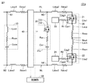
図1を参照して、電力変換装置100は、高電圧側の電力線PL及び低電圧側の電力線NLと、直流コンデンサ10と、レグ20と、ゲートドライバ23,24とを備える。高電圧側の電力線PL及び低電圧側の電力線NLは、図示しない直流電源の正極側及び負極側と接続される。直流コンデンサ10は、電力線PL上のノードN1及び電力線NL上のノードN2の間に接続される。
Referring to FIG. 1,
レグ20は、ノードNoutを介して、電力線PL及びNLの間に直列に接続された、半導体スイッチング素子21及び22を有する。ノードNoutは、レグ20の「出力端」に相当し、図示しないインダクタ及び/又はコンデンサ等を介して負荷に接続される。
The
半導体スイッチング素子21は、スイッチS1と、スイッチS1に対して逆並列に接続されたダイオードD1とを含む。スイッチS1の制御電極(ゲート)は、ゲート抵抗R1を介してゲートドライバ23に接続される。同様に、半導体スイッチング素子22は、スイッチS2と、スイッチS2に対して逆並列に接続されたダイオードD2とを含む。スイッチS2の制御電極(ゲート)は、ゲート抵抗R2を介してゲートドライバ24に接続される。ゲート抵抗R1及びR2は、通常、抵抗素子を配置することによって形成される。
The
ゲートドライバ23及び24は、スイッチS1及びS2をオンオフするための駆動信号を出力する。一般的には、駆動信号は、同一のレグ20を構成する半導体スイッチング素子21及び22を相補にオンオフするための電圧パルスとして生成される。なお、本明細書では、スイッチS1のオンオフについて、半導体スイッチング素子21のオンオフとも称する。同様に、スイッチS2のオンオフについて、半導体スイッチング素子22のオンオフとも称する。
The
半導体スイッチング素子21,22は、ゲートドライバ23及び24からの駆動信号によってオンオフ制御可能な、MOS(Metal Oxide Semiconductor)−FET又はIGBT(Insulated Gate Bipolar Transistor)等によって構成することができる。又、半導体スイッチング素子21,22は、シリコン材料を用いて構成されてもよく、炭化珪素(NiC)や窒化ガリウム(GaN)、酸化ガリウム(Ga2O3)、ダイヤモンド等のワイドバンドギャップ半導体を用いて構成することも可能である。The
図2には、図1に示した基本構成の等価回路図が示される。図2中には、回路内の寄生成分がさらに表記されている。 FIG. 2 shows an equivalent circuit diagram of the basic configuration shown in FIG. In FIG. 2, parasitic components in the circuit are further shown.
図2を参照して、電力線PL上のノードN1及び電力線NL上のノードN2の間には、直流コンデンサ10及び配線群によって、容量成分Ccon、抵抗成分Rcon、及び、誘導成分Lconが存在する。誘導成分Lcon及び抵抗成分Rconは、直流コンデンサ10のESL(Equivalent Series Inductance)及びESR(Equivalent Series Resistance)に相当する。
Referring to FIG. 2, between the node N1 on the power line PL and the node N2 on the power line NL, a capacitance component Ccon, a resistance component Rcon, and an inductive component Lcon exist due to the
又、ノードN1と、電力線PLと接続される半導体スイッチング素子21のドレイン端子との間には、抵抗成分Rdcp及び誘導成分Ldcpが存在する。同様に、ノードN2と、電力線NLと接続された半導体スイッチング素子22のソース端子との間には、抵抗成分Rdcn及び誘導成分Ldcnが存在する。
A resistance component Rdcp and an induction component Ldcp exist between the node N1 and the drain terminal of the
ノードNoutと、ノードNoutと接続された半導体スイッチング素子21のソース端子との間には、抵抗成分Racp及び誘導成分Lacpが存在する。同様に、ノードNoutと、ノードNoutと接続された半導体スイッチング素子22のドレイン端子との間には、抵抗成分Racn及び誘導成分Lacnが存在する。
A resistance component Racp and an inductive component Lacp exist between the node Nout and the source terminal of the
さらに、半導体スイッチング素子21の容量成分は、ドレイン−ソース間寄生容量Cds1と、ドレイン−ゲート間寄生容量Cdg1と、ゲート−ソース間寄生容量Cgs1とで表される。図2に示されるように、Cdg1及びCgs1の直列回路が、Cds1と並列に接続された構成となる。
Furthermore, the capacitance component of the
同様に、半導体スイッチング素子22の容量成分は、ドレイン−ソース間寄生容量Cds2と、ドレイン−ゲート間寄生容量Cdg2と、ゲート−ソース間寄生容量Cgs2とで表される。そして、Cdg2及びCgs2の直列回路がCds2と並列に接続された構成となる。
Similarly, the capacitance component of the
図2に示されるように、電力変換装置100の基本構成により、半導体スイッチング素子21のオン時には、直流コンデンサ10、電力線PL、半導体スイッチング素子21(オン状態)、ノードNout、半導体スイッチング素子22のドレイン−ソース間寄生容量Cds2、及び、電力線NLによって主回路ループMLP1が構成される。一方で、半導体スイッチング素子22のオン時には、直流コンデンサ10、電力線PL、半導体スイッチング素子21のドレイン−ソース間寄生容量Cds1、ノードNout、半導体スイッチング素子22(オン状態)、及び、電力線NLによって主回路ループMLP2が構成される。通常、半導体スイッチング素子21及び22の特性は共通に設計されるので、以下では、主回路ループMLP1及びMLP2を包括的に表記する場合には、主回路ループMLPとも称する。
As shown in FIG. 2, when the
主回路ループMLPは、図2中に示した寄生成分による共振回路を形成する。このため、半導体スイッチング素子21又は22のターンオフ時に、当該共振回路の共振周波数近傍の電圧変動が生じると、当該電圧変動が持続することにより、ターンオフ後にターンオン及びターンオフを周期的に繰り返す、連鎖的誤動作現象が発生する虞がある。当該連鎖的誤動作現象は、特に、ターンオンする電圧閾値が低い半導体スイッチング素子で起こり易い。又、高速スイッチングする半導体スイッチング素子についても、スイッチング周波数が寄生成分による共振周波数に近付く傾向にあるため、連鎖的誤動作現象が起こり易くなる。これらの観点から、半導体スイッチング素子21,22が、上述のワイドギャップ半導体を用いて構成されるときに、連鎖的誤動作現象が発生し易くなることが理解される。
The main circuit loop MLP forms a resonance circuit due to the parasitic component shown in FIG. For this reason, when the
本発明の実施の形態1による電力変換装置の構成について、図3〜図6を用いて説明する。 The configuration of the power converter according to the first embodiment of the present invention will be described with reference to FIGS.
図3は、実施の形態1による電力変換装置の構成の第1の例を示す回路図である。
図3を参照して、実施の形態1の第1の例に係る電力変換装置100aは、図1及び図2に示された基本構成に加えて、連鎖的誤動作を抑制するための減衰器30aをさらに備える。FIG. 3 is a circuit diagram showing a first example of the configuration of the power conversion device according to the first embodiment.
Referring to FIG. 3,
減衰器30aは、電力線PL上のノードN3と、電力線NL上のノードN4との間に接続される。すなわち、減衰器30aは、レグ20及び直流コンデンサ10に対して並列接続される。
ノードN3は、ノードN1及び半導体スイッチング素子21のドレイン端子の間に位置する。同様に、ノードN4は、ノードN2及び半導体スイッチング素子22のソース端子の間に位置する。これにより、図2に示した抵抗成分Rdcpと誘導成分Ldcpとは、ノードN3を境に、抵抗成分Rdcp1及びRdcp2(Rdcp=Rdcp1+Rdcp2)と、誘導成分Ldcp1及びLdcp2(Ldcp=Ldcp1+Ldcp2)とに分割される。同様に、図2に示した抵抗成分Rdcnと誘導成分Ldcnとは、ノードN4を境に、抵抗成分Rdcn1及びRdcn2(Rdcn=Rdcn1+Rdcn2)と、誘導成分Ldcn1及びLdcn2(Ldcn=Ldcn1+Ldcn2)とに分割される。
The node N3 is located between the node N1 and the drain terminal of the
図4には、図3に示された減衰器30aの構成例が示される。
図4を参照して、減衰器30aは、いわゆるスナバ回路を構成する、抵抗素子Rsn及びコンデンサCsnの直列回路を有する。抵抗素子Rsn及びコンデンサCsnは、ノードN3及びN4の間に電気的に接続される。なお、以下では、抵抗素子Rsnの抵抗値についてもRsnと表記し、コンデンサCsnの容量値についてもCsnと表記する。FIG. 4 shows a configuration example of the
Referring to FIG. 4, the
減衰器30aは、直流コンデンサ10のESL(Equivalent Series Inductance)を含むループインダクタンスと、半導体スイッチング素子21,22とを含む主回路ループMLP1,MLP2(図2)による共振を減衰するために、主回路ループMLP1及びMLP2に対して電気的に接続される。
The
主回路ループMLP1及びMLP2に対して並列接続される減衰器30aは、カットオフ周波数fcが、主回路ループMLPの共振周波数frよりも低くなるように構成される。
The
主回路ループMLPの共振周波数frは、半導体スイッチング素子21及び22のドレイン−ソース間容量について、Cds1=Cds2=Cdsとすると、下記の式(1)で示される。
The resonance frequency fr of the main circuit loop MLP is represented by the following formula (1), where Cds1=Cds2=Cds is set for the drain-source capacitances of the
fr=1/(2・π・√(Lr・Cds)) …(1)
但し、Lr=Lcon+Ldcp+Lacp+Lacn+Ldcn
又、減衰器30aのカットオフ周波数fcは、下記の式(2)で示される。fr=1/(2·π·√(Lr·Cds)) (1)
However, Lr=Lcon+Ldcp+Lacp+Lacn+Ldcn
The cutoff frequency fc of the
fc=1/(2・π・Rsn・Csn) …(2)
即ち、減衰器30aの回路定数Rsn及びCsnが、fc<frとなるように決められることにより、主回路ループMLPの共振周波数におけるアドミタンスを低下することができる。この結果、ターンオフ時に主回路ループMLP内に生じた電圧変動の減衰効果を高めることで、半導体スイッチング素子21,22の連鎖的誤動作現象を抑制することが可能となる。fc=1/(2·π·Rsn·Csn) (2)
That is, by determining the circuit constants Rsn and Csn of the
図5は、実施の形態1による電力変換装置の構成の第2の例を示す回路図である。
図5を参照して、実施の形態1の第2の例に係る電力変換装置100bは、図3に示された電力変換装置100aと比較して、減衰器30aに代えて減衰器30bを備える点で異なる。減衰器30bは、レグ20及び直流コンデンサ10に対して直列接続される。例えば、減衰器30bは、電力線PLに介挿接続される。これにより、図2に示した抵抗成分Rdcpと誘導成分Ldcpとは、減衰器30bを境に、抵抗成分Rdcp1及びRdcp2(Rdcp=Rdcp1+Rdcp2)と、誘導成分Ldcp1及びLdcp2(Ldcp=Ldcp1+Ldcp2)とに分割される。FIG. 5 is a circuit diagram showing a second example of the configuration of the power conversion device according to the first embodiment.
Referring to FIG. 5,
図6には、図5に示された減衰器30bの構成例が示される。
図6を参照して、減衰器30bは、トランスTrと、磁気スナバ34とを含む。トランスTrは、電力線PLと直列接続された一次巻線41、及び、一次巻線41と磁気的に結合する二次巻線42を有する。一次巻線41及び二次巻線42の間は、電気的に絶縁される。磁気スナバ34は、二次巻線42と直列に接続され、例えば、リアクタンスを可変制御可能な可飽和リアクトルや、高周波域で抵抗成分が支配的となるフェライトビーズ等によって構成することができる。FIG. 6 shows a configuration example of the
Referring to FIG. 6, the
減衰器30bについては、トランスを用いない構成とすることも可能である。この場合には、リアクタンスを可変制御可能な可飽和リアクトル、又は、高周波域で抵抗成分が支配的となるフェライトビーズ等を、減衰器30bとして電力線PL又はNL上に直列に接続することができる。又は、高周波域で抵抗成分が支配的となる様な特性を有するフェライト材等で製作されたリング状のコアを、電力線PL又はNLを周回するように配置することによって、減衰器30bを構成することも可能である。
The
主回路ループMLPに対して直列接続される減衰器30bは、主回路ループMLPの共振周波数frにおけるインピーダンスが、半導体スイッチング素子21,22のスイッチング周波数におけるインピーダンスよりも高くなるように構成される。言い換えると、このような周波数特性が実現されるように、磁気スナバ34が選定される。
The
減衰器30bの配置により、半導体スイッチング素子21,22のスイッチングによる主回路ループMLPでの電力損失を抑制するとともに、主回路ループMLPの共振周波数におけるアドミタンスを低下することができる。この結果、通常のスイッチング動作における効率を低下させることなく、ターンオフ時に主回路ループMLP内に生じた電圧変動の減衰効果を高めることで、半導体スイッチング素子21,22の連鎖的誤動作現象を抑制することが可能となる。
By disposing the
なお、減衰器30bは、主回路ループMLPに対して直列接続されるのであれば、電力線NLに介挿接続されてもよく、直流コンデンサ10と電力線PL又はNLとの間に接続されてもよい。さらに、減衰器30bは、半導体スイッチング素子21と電力線PLの間、半導体スイッチング素子21或いは22とノードNoutとの間、又は、半導体スイッチング素子22及び電力線NLの間に、接続されてもよい。又、減衰器30bは、複数個所に配置されてもよい。即ち、減衰器30bは、電力線PL及びNLの少なくとも一方に設けることができる。
It should be noted that the
このように実施の形態1に係る電力変換装置100a,100bでは、主回路ループMLPに対して並列接続される減衰器30a、及び、主回路ループMLPに対して直列接続される減衰器30bの少なくとも一方が配置される。即ち、減衰器30a及び30bの両方を、主回路ループMLPに対して接続することも可能である。
As described above, in the
これにより、主回路ループMLPの共振周波数におけるアドミタンスを低下させて電圧変動の減衰効果を高めることにより、半導体スイッチング素子21,22の連鎖的誤動作現象を抑制することが可能となる。この結果、レグを構成する半導体スイッチング素子を高速にオンオフさせても、電力変換装置を安定的に定常動作させることが可能となる。
As a result, the admittance at the resonance frequency of the main circuit loop MLP is reduced to enhance the damping effect of the voltage fluctuation, so that the chain malfunction phenomenon of the
なお、上述のように、本実施の形態において半導体スイッチング素子21,22の半導体材料は制限されるものではないが、GaN等のワイドギャップ半導体が用いられた、低電圧閾値及び高速スイッチングを特徴とする半導体スイッチング素子についても、連鎖的誤動作の発生を効果的に抑制することが可能となる。
As described above, the semiconductor material of the
実施の形態2.
図7は、実施の形態2による電力変換装置の構成の第1の例を示す回路図である。
FIG. 7 is a circuit diagram showing a first example of the configuration of the power conversion device according to the second embodiment.
図7を参照して、実施の形態2の第1の例に係る電力変換装置101aは、図3及び図4に示された電力変換装置100aと比較して、検出部40及び制御部50をさらに備える点、並びに、減衰器30aに代えて減衰器31aを備える点で異なる。
Referring to FIG. 7,
検出部40は、電力線PL,NLの電圧及び/又は電流を検出するように構成される。例えば、検出部40によって、直流コンデンサ10の電圧、及び/又は、直流コンデンサ10とレグ20との間の電流を検出することが可能である。
The
減衰器31aは、減衰器30a(図4)と比較して、抵抗素子Rsn及びコンデンサCsnと直列に接続された補助スイッチ素子35を含む。補助スイッチ素子35は、スイッチS3と、スイッチS3に対して逆並列に接続されたダイオードD3とを含む。
The
スイッチS3は、制御部50からの制御信号に従ってオンオフされる。以下では、スイッチS3のオンオフを補助スイッチ素子35のオンオフとも称する。補助スイッチ素子35は、トランジスタ(例えば、MOS−FET)等によって構成することができる。
The switch S3 is turned on/off according to a control signal from the
制御部50には、検出部40による検出値が入力される。従って、制御部50は、検出部40による電圧及び/又は電流の検出値に従って、減衰器31a中の補助スイッチ素子35の制御信号を生成する。
The detection value of the
減衰器31aは、補助スイッチ素子35のオン時には、主回路ループMLPに対して、実施の形態1で説明した減衰器30aと同等に機能する。一方で、補助スイッチ素子35のオフ時には、減衰器31a中の抵抗素子Rsn及びコンデンサCsnの電流通過が遮断される。即ち、補助スイッチ素子35のオフ期間では、減衰器31aによる電力損失が発生しない。
When the
制御部50は、例えば、検出部40によって検出された電圧及び/又は電流が、予め定められた閾値よりも大きいときに、補助スイッチ素子35をオンする一方で、それ以外では、補助スイッチ素子35をオフするように、補助スイッチ素子35の制御信号を生成する。一般的に、半導体スイッチング素子21,22の連鎖的誤動作は、大電圧及び大電流のスイッチング時に発生する可能性が高いので、当該閾値は、半導体スイッチング素子21,22の特性に応じて、連鎖的誤動作が発生し易い動作領域(電圧/電流)の境界に対応させて予め定めることができる。
For example, the
或いは、検出部40は、図8に示す変形例のように配置することも可能である。
図8を参照して、検出部40は、電力線NL及びノードNoutから図示しない負荷に供給される電圧及び/又は電流を検出することが可能である。図8の検出部40の配置個所以外の点は、図7と同様であるので、詳細な説明は繰り返さない。Alternatively, the
With reference to FIG. 8, the
即ち、制御部50は、検出部40によって検出された電圧及び/又は電流(すなわち、レグ20から負荷へ供給される電圧及び/又は電流)に基づいて、例えば、予め定められた閾値との比較に従って、減衰器31a中の補助スイッチ素子35のオンオフを制御することができる。
That is, the
実施の形態2の第1の例に係る電力変換装置101aによれば、連鎖的誤動作が発生しない動作条件では、主回路ループMLPに対して並列接続された減衰器31aを、電流経路から切り離すことができる。この結果、実施の形態1に係る電力変換装置による連鎖的誤動作の抑制効果に加えて、減衰器31aによる電力損失を、減衰器30aと比較して、低減することができる。
According to the
図9は、実施の形態2による電力変換装置の構成の第2の例を示す回路図である。
図9を参照して、実施の形態2の第2の例に係る電力変換装置101bは、図5及び図6に示された電力変換装置100bと比較して、検出部40及び制御部50をさらに備える点、及び、減衰器30bに代えて減衰器31bを備える点で異なる。減衰器31bは、主回路ループに対して直列接続される限り任意の個所に配置できるが、図9の例では、電力線NLに介挿接続される。減衰器31bは、減衰器30bと同様に、電力線PL及びNLの少なくとも一方に設けることができる。FIG. 9 is a circuit diagram showing a second example of the configuration of the power conversion device according to the second embodiment.
With reference to FIG. 9, a
減衰器31bは、減衰器30b(図6)と比較して、二次巻線42及び磁気スナバ34に対して直列接続された補助スイッチ素子35を含む。補助スイッチ素子35は、制御部50からの制御信号に従ってオンオフされる。補助スイッチ素子35は、トランジスタ(例えば、MOS−FET)等によって構成することができる。
The
減衰器31bは、補助スイッチ素子35のオン時には、主回路ループMLPに対して、実施の形態1で説明した減衰器30bと同等に機能する。一方で、補助スイッチ素子35のオフ時には、減衰器31b中の磁気スナバ34の電流通過が遮断されるので、磁気スナバ34による電力損失が発生しなくなる。
When the
尚、上述したように、トランスを用いずに、可飽和リアクトル又はフェライトビーズ等を電力線PL又はNL上に直列に接続することで減衰器30bを構成した場合には、補助スイッチ素子35を、当該減衰器30bの構成要素と並列に電力線PL又はNLと接続することで、減衰器31bを構成することが可能である。この場合には、補助スイッチ素子35のオン時に、当該減衰器30bの構成要素をバイパスした経路を、電力線PL又はNLにおいて形成することで、当該構成要素での電力損失が発生しなくなる。
As described above, when the
検出部40は、図7と同様に配置されて、電力線PL,NLの電圧及び/又は電流を検出するように構成される。制御部50には、検出部40による検出値が入力される。
The
或いは、検出部40は、図10に示す変形例のように配置することも可能である。
図10を参照して、検出部40は、図8と同様に、電力線NL及びノードNoutから図示しない負荷に供給される電圧及び/又は電流を検出することが可能である。図10の検出部40の配置個所以外の点は、図8と同様であるので、詳細な説明は繰り返さない。Alternatively, the
With reference to FIG. 10, the
図9及び図10において、制御部50は、図7及び図8と同様に、検出部40による電圧及び/又は電流の検出値に基づいて、例えば、検出値と予め定められた閾値との比較に従って、減衰器31b中の補助スイッチ素子35の制御信号を生成する。
9 and 10, the
従って、実施の形態2の第2の例に係る電力変換装置101bによれば、連鎖的誤動作が発生しない動作条件では、主回路ループMLPに対して直列接続された減衰器31bにおいて、磁気スナバ34の電流を遮断できる。この結果、実施の形態1に係る電力変換装置による連鎖的誤動作の抑制効果に加えて、減衰器31bによる電力損失を、減衰器30bと比較して、低減することができる。
Therefore, according to the
このように、実施の形態2に係る電力変換装置101a,101bでは、主回路ループMLPに対して並列接続される減衰器31a、及び、主回路ループMLPに対して直列接続される減衰器31bの少なくとも一方が配置される。即ち、減衰器31a及び31bの両方を、主回路ループMLPに対して接続することも可能である。
As described above, in the
この結果、実施の形態2に係る電力変換装置100a,100bによる効果に加えて、連鎖的誤動作を抑制するための減衰器31a,31bに電流が生じる期間を、連鎖的誤動作が発生する可能性が高い動作状態である期間に限定するので、電力損失を低減して、高効率の電力変換を実行することが可能である。
As a result, in addition to the effect of the
実施の形態2については、半導体スイッチング素子21,22について、連鎖的誤動作が発生する動作状態(動作領域)が予め把握されている場合に、特に有効に適用することができる。
The second embodiment can be particularly effectively applied to the
実施の形態2の変形例.
図11は、実施の形態2の変形例による電力変換装置の構成の第1の例を示す回路図である。Modification of the second embodiment.
FIG. 11 is a circuit diagram showing a first example of the configuration of the power conversion device according to the modification of the second embodiment.
図11を参照して、減衰器31a及び制御部50が配置された電力変換装置101aにおいて、検出部40は、半導体スイッチング素子22と、ノードNoutとの間に配置される。これにより、検出部40は、半導体スイッチング素子22に流れる電流を直接検出することができる。或いは、検出部40は、ノードN4と半導体スイッチング素子22との間に配置されてもよい。
Referring to FIG. 11, in
制御部50には、検出部40による検出値(半導体スイッチング素子22の通過電流)に加えて、ゲートドライバ24から出力される半導体スイッチング素子22の駆動信号(電圧パルス)がさらに入力される。
The
制御部50は、駆動信号に従って判断された半導体スイッチング素子22のオフ期間において、半導体スイッチング素子22に順方向の電流が生じているときに、連鎖的誤動作が発生していると判断して、減衰器31a内の補助スイッチ素子35をオンすることができる。一方で、それ以外の期間、即ち、駆動信号に従って判断された半導体スイッチング素子22のオン期間、及び、半導体スイッチング素子22のオフ期間中に半導体スイッチング素子22に順方向電流が生じていないときには、補助スイッチ素子35をオフ状態とすることができる。
The
尚、図11では、半導体スイッチング素子22の電流を検出するように検出部40を配置する例を示したが、半導体スイッチング素子21の電流を直接検出するように、半導体スイッチング素子21及びノードNoutの間、又は、ノードN3及び半導体スイッチング素子21の間に検出部40を配置することも可能である。この場合には、制御部50には、ゲートドライバ23から出力される駆動信号(電圧パルス)がさらに入力される。さらに、制御部50は、駆動信号に従って判断された半導体スイッチング素子21のオフ期間において、半導体スイッチング素子21に順方向の電流が生じているときに、減衰器31a内の補助スイッチ素子35をオンするとともに、それ以外の期間では補助スイッチ素子35をオフ状態とすることができる。
Note that, although FIG. 11 shows an example in which the
図12は、実施の形態2の変形例による電力変換装置の構成の第2の例を示す回路図である。 FIG. 12 is a circuit diagram showing a second example of the configuration of the power conversion device according to the modification of the second embodiment.
図12を参照して、減衰器31a及び制御部50が配置された電力変換装置101aにおいて、検出部40は半導体スイッチング素子22のドレイン−ソース間と並列に配置される。これにより、検出部40は、半導体スイッチング素子22の印加電圧を直接検出することができる。さらに、検出部40は、図7と同様に、電力線PL,NLの間にも配置される。これにより、直流コンデンサ10の電圧が検出される。
Referring to FIG. 12, in
図11と同様に、制御部50には、検出部40による検出値(半導体スイッチング素子22への印加電圧、及び、直流コンデンサ10の電圧)に加えて、ゲートドライバ24から出力される駆動信号(電圧パルス)がさらに入力される。
Similar to FIG. 11, the
制御部50は、駆動信号に従って判断された半導体スイッチング素子22のオフ期間において、半導体スイッチング素子22のドレイン−ソース間電圧が直流コンデンサ10の電圧よりも小さい場合に、連鎖的誤動作が発生していると判断して、補助スイッチ素子35をオン状態とすることができる。一方で、制御部50は、それ以外の期間において、補助スイッチ素子35をオフ状態とすることができる。即ち、駆動信号に従って判断された半導体スイッチング素子22のオン期間には、補助スイッチ素子35はオフ状態に維持される。
When the drain-source voltage of the
或いは、検出部40は、電力線PL,NL間に加えて、半導体スイッチング素子21のドレイン−ソース間と並列に配置することも可能である。この場合には、検出部40は、半導体スイッチング素子21の印加電圧を直接検出することが可能となる。この場合には、制御部50には、ゲートドライバ23から出力される駆動信号(電圧パルス)がさらに入力される。さらに、制御部50は、駆動信号に従って判断された半導体スイッチング素子21のオフ期間において、半導体スイッチング素子22のドレイン−ソース間電圧が直流コンデンサ10の電圧よりも小さい場合に、減衰器31a内の補助スイッチ素子35をオンするとともに、それ以外の期間では補助スイッチ素子35をオフ状態とすることができる。
Alternatively, the
尚、図11及び図12では、半導体スイッチング素子21及び22の一方のみに対応して検出部40を配置したが、半導体スイッチング素子21及び22の両方に対応して検出部40を配置することも可能である。この場合には、制御部50は、ゲートドライバ23及び24から出力された駆動信号に基づいて判断された、半導体スイッチング素子21,22のオフ期間における半導体スイッチング素子21,22の電圧又は電流に従って、連鎖的誤動作が発生していると判断した場合に、補助スイッチ素子35をオン状態とすることができる。
Although the
このように、実施の形態2の変形例によれば、半導体スイッチング素子21,22の電流又は電圧の検出値に基づいて、実際に、半導体スイッチング素子21,22のオフ期間中に連鎖的誤動作が発生していると判断されるような電圧挙動又は電流挙動が検知された場合に限って、補助スイッチ素子35がオンされて、主回路ループMLPの共振周波数におけるアドミタンスの低減が図られる。この結果、実施の形態2で説明した効果に加えて、減衰器31a,31bの作動を最低限として、電力損失をさらに低減することが可能となる。
As described above, according to the modification of the second embodiment, a chained malfunction actually occurs during the off period of the
又、減衰器31a及び制御部50が配置された電力変換装置101b(図9及び図10)に対しても、図11及び図12で説明した変形例を適用することが可能である。具体的には、半導体スイッチング素子21及び/又は22の電圧又は電流を検出するように検出部40を配置することによって、制御部50は、半導体スイッチング素子21,22のオフ期間中に連鎖的誤動作が発生していると判断されるような電圧挙動又は電流挙動が検知された場合に限って、減衰器31b中の補助スイッチ素子35をオンすることができる。
Further, the modified examples described in FIGS. 11 and 12 can be applied to the
実施の形態3.
実施の形態3では、複数のレグが並列接続された電力変換装置における連鎖的誤動作の抑制について説明する。
In the third embodiment, suppression of chain malfunction in a power conversion device in which a plurality of legs are connected in parallel will be described.
図13は、実施の形態3が適用される電力変換装置の基本構成を示す回路図である。
図13を参照して、電力変換装置102は、高電圧側の電力線PL及び低電圧側の電力線NLと、直流コンデンサ10と、複数のレグ20a及び20bと、ゲートドライバ23,24とを備える。高電圧側の電力線PL及び低電圧側の電力線NLは、図示しない直流電源の正極側及び負極側と接続される。FIG. 13 is a circuit diagram showing the basic configuration of the power conversion device to which the third embodiment is applied.
Referring to FIG. 13,
レグ20aは、ノードNoutaを介して、電力線PL上のノードNx及び電力線NL上のノードNyの間に直列に接続された、半導体スイッチング素子21a及び22aを有する。半導体スイッチング素子21aは、スイッチS1aと、スイッチS1aに対して逆並列に接続されたダイオードD1aとを含む。スイッチS1aの制御電極(ゲート)は、ゲート抵抗R1aを介してゲートドライバ23に接続される。同様に、半導体スイッチング素子22aは、スイッチS2aと、スイッチS2aに対して逆並列に接続されたダイオードD2aとを含む。スイッチS2aの制御電極(ゲート)は、ゲート抵抗R2aを介してゲートドライバ24に接続される。
The
同様に、レグ20bは、ノードNoutbを介して、電力線PL(ノードNx)及び電力線NL(ノードNy)の間に直列に接続された、半導体スイッチング素子21b及び22bを有する。半導体スイッチング素子21bは、半導体スイッチング素子21と同様に構成されて、スイッチS1bと、スイッチS1bに対して逆並列に接続されたダイオードD1bとを含む。スイッチS1bの制御電極(ゲート)は、ゲート抵抗R1bを介してゲートドライバ23に接続される。
Similarly, the
同様に、半導体スイッチング素子22bは、半導体スイッチング素子22と同様に構成されて、スイッチS2bと、スイッチS2bに対して逆並列に接続されたダイオードD2bとを含む。スイッチS2bの制御電極(ゲート)は、ゲート抵抗R2bを介してゲートドライバ24に接続される。
Similarly, the
スイッチS1a及びS1bは、ゲート抵抗R1a及びR2aを介して共通のゲートドライバ23と接続され、スイッチS2a及びS2bは、ゲート抵抗R1b及びR2bを介して共通のゲートドライバ24と接続される。これにより、並列接続された半導体スイッチング素子21a及び21bは共通にオンオフ制御される。同様に、半導体スイッチング素子22a及び22bは共通にオンオフ制御される。
The switches S1a and S1b are connected to the
このように、複数のレグ20a及び20bは、電力線PL及びNLに対して並列接続されて、共通にオンオフ制御される。又、ノードNouta及びNoutbは、レグ20a及び20bの「出力端」に相当し、図示しないインダクタ及び/又はコンデンサ等を介して負荷に接続される。
In this way, the plurality of
図14には、図3に示した構成の等価回路図が示される。図14中には、回路内の寄生成分がさらに表記されている。 FIG. 14 shows an equivalent circuit diagram of the configuration shown in FIG. In FIG. 14, parasitic components in the circuit are further shown.
図14を参照して、レグ20aでは、半導体スイッチング素子21aにおいて、ドレイン−ソース間寄生容量Cds1a、ドレイン−ゲート間寄生容量Cdg1a、及び、ゲート−ソース間寄生容量Cgs1aが容量成分として存在する。Cdg1a及びCgs1aの直列回路が、Cds1aと並列に接続された構成となる。同様に、半導体スイッチング素子22aでは、ドレイン−ソース間寄生容量Cds2a、ドレイン−ゲート間寄生容量Cdg2a、及び、ゲート−ソース間寄生容量Cgs2aが容量成分として存在する。Cdg2a及びCgs2aの直列回路が、Cds2aと並列に接続された構成となる。
Referring to FIG. 14, in the
同様に、レグ20bでは、半導体スイッチング素子21bにおいて、ドレイン−ソース間寄生容量Cds1b、ドレイン−ゲート間寄生容量Cdg1b、及び、ゲート−ソース間寄生容量Cgs1bが容量成分として存在する。Cdg1b及びCgs1bの直列回路が、Cds1bと並列に接続された構成となる。同様に、半導体スイッチング素子22bでは、ドレイン−ソース間寄生容量Cds2b、ドレイン−ゲート間寄生容量Cdg2b、及び、ゲート−ソース間寄生容量Cgs2bが容量成分として存在する。Cdg2b及びCgs2bの直列回路が、Cds2bと並列に接続された構成となる。
Similarly, in the
図3に加えて、ノードNxと、半導体スイッチング素子21aのドレイン端子との間には、抵抗成分Rdcpa及び誘導成分Ldcpaが存在し、ノードNxと、半導体スイッチング素子22aのドレイン端子との間には、抵抗成分Rdcpb及び誘導成分Ldcpbが存在する。又、ノードNyと、半導体スイッチング素子22aのソース端子との間には、抵抗成分Rdcna及び誘導成分Ldcnaが存在し、ノードNyと、半導体スイッチング素子22bのソース端子との間には、抵抗成分Rdcnb及び誘導成分Ldcnbが存在する。
In addition to FIG. 3, a resistance component Rdcpa and an induction component Ldcpa exist between the node Nx and the drain terminal of the
同様に、図3に加えて、ノードNoutaと、半導体スイッチング素子21aのソース端子との間には、抵抗成分Racpa及び誘導成分Lacpaが存在し、ノードNoutbと、半導体スイッチング素子22aのドレイン端子との間には、抵抗成分Racna及び誘導成分Lacnaが存在する。同様に、ノードNoutbと、半導体スイッチング素子21bのソース端子との間には、抵抗成分Racpb及び誘導成分Lacpbが存在し、ノードNoutbと、半導体スイッチング素子22bのドレイン端子との間には、抵抗成分Racnb及び誘導成分Lacnbが存在する。
Similarly, in addition to FIG. 3, a resistance component Racpa and an induction component Lacapa exist between the node Nouta and the source terminal of the
上述のように、半導体スイッチング素子21a及び21bは、ゲートドライバ23からの駆動信号によって共通にオンオフし、半導体スイッチング素子22a及び22bは、ゲートドライバ24からの駆動信号によって共通にオンオフする。
As described above, the
半導体スイッチング素子21a及び21bのオン時には、半導体スイッチング素子22a及び22bはオフされるので、直流コンデンサ10、電力線PL、半導体スイッチング素子21a,22a(オン状態)、ノードNouta,Noutb、半導体スイッチング素子22a,22bのドレイン−ソース間寄生容量Cds2a,Cds2b、及び、電力線NLによって、図2での主回路ループMLP1に相当する主回路ループが形成される。
Since the
一方で、半導体スイッチング素子22a及び22bのオン時には、半導体スイッチング素子21a及び21bはオフされるので、直流コンデンサ10、電力線PL、半導体スイッチング素子21a,21bのドレイン−ソース間寄生容量Cds1a,Cds1b、ノードNout,半導体スイッチング素子22a,22b(オン状態)、及び、電力線NLによって、図2での主回路ループMLP2に相当する主回路ループが形成される。
On the other hand, when the
複数のアームを並列接続した構成においても、上述の主回路ループは、図13中に示した寄生成分による共振回路を形成することが理解される。但し、実施の形態3での当該共振回路では、Ldcpa+Lacpa及びLdcpb+Lacpb、並びに、Ldcna+Lacna及びLdcnb+Lacnbが並列接続されるとともに、Cds2a及びCds2b、又は、Cds1a及びCds1bが並列接続されることを考慮して、式(1)と同様の考え方で共振周波数fr♯を求めることができる。 It is understood that even in a configuration in which a plurality of arms are connected in parallel, the main circuit loop described above forms a resonance circuit due to the parasitic component shown in FIG. However, in the resonant circuit according to the third embodiment, it is considered that Ldcpa+Lacpa and Ldcpb+Lacpb, and Ldcna+Lacna and Ldcnb+Lacnb are connected in parallel, and Cds2a and Cds2b, or Cds1a and Cds1b are connected in parallel. The resonance frequency fr# can be obtained in the same way as in (1).
図15は、実施の形態3による電力変換装置の構成の第1の例を示す回路図である。
図15を参照して、実施の形態3の第1の例に係る電力変換装置102aは、図13及び図14に示された基本構成に加えて、図3と同様の減衰器30aをさらに備える。FIG. 15 is a circuit diagram showing a first example of the configuration of the power conversion device according to the third embodiment.
Referring to FIG. 15,
減衰器30aは、図3と同様に、電力線PL上のノードN3と、電力線NL上のノードN4との間に接続される。減衰器30aは、複数のレグ20a,20b及び直流コンデンサ10に対して並列接続される。
The
ノードN3は、ノードN1及びNxの間に位置し、ノードN4は、ノードN2及びNyの間に位置する。図3と同様に、電力線PLの抵抗成分Rdcpと誘導成分Ldcpとは、ノードN3を境に、抵抗成分Rdcp1及びRdcp2(Rdcp=Rdcp1+Rdcp2)と、誘導成分Ldcp1及びLdcp2(Ldcp=Ldcp1+Ldcp2)とに分割される。同様に、電力線NLの抵抗成分Rdcnと誘導成分Ldcnとは、ノードN4を境に、抵抗成分Rdcn1及びRdcn2(Rdcn=Rdcn1+Rdcn2)と、誘導成分Ldcn1及びLdcn2(Ldcn=Ldcn1+Ldcn2)とに分割される。 The node N3 is located between the nodes N1 and Nx, and the node N4 is located between the nodes N2 and Ny. Similar to FIG. 3, the resistance component Rdcp and the induction component Ldcp of the power line PL are divided into the resistance components Rdcp1 and Rdcp2 (Rdcp=Rdcp1+Rdcp2) and the induction components Ldcp1 and Ldcp2 (Ldcp=Ldcp1+Ldcp2) with the node N3 as a boundary. To be done. Similarly, the resistance component Rdcn and the induction component Ldcn of the power line NL are divided into the resistance components Rdcn1 and Rdcn2 (Rdcn=Rdcn1+Rdcn2) and the induction components Ldcn1 and Ldcn2 (Ldcn1+Ldcn2) with the node N4 as a boundary.
図15に示すように接続された減衰器30aのカットオフ周波数fcを上記共振周波数fr♯よりも低くすることによって、ターンオフ時に主回路ループMLP内に生じた電圧変動の減衰効果を高めることができる。
By setting the cutoff frequency fc of the
この結果、実施の形態3によれば、複数のレグ20a,20bが並列接続された構成においても、半導体スイッチング素子21a,21b,22a,22bの連鎖的誤動作現象を抑制することが可能となる。
As a result, according to the third embodiment, it is possible to suppress the chain malfunction phenomenon of the
図16は、実施の形態3による電力変換装置の構成の第2の例を示す回路図である。
図16を参照して、実施の形態3の第2の例に係る電力変換装置102bは、図13及び図14に示された基本構成に加えて、図5と同様の減衰器30bをさらに備える。FIG. 16 is a circuit diagram showing a second example of the configuration of the power conversion device according to the third embodiment.
Referring to FIG. 16, a
減衰器30bは、レグ20a,20bの両方、及び、直列コンデンサに対して直列接続される。例えば、減衰器31b1を電力線PLに介挿接続することで、図5と同様に、抵抗成分Rdcpと誘導成分Ldcpとは、減衰器30bを境に、抵抗成分Rdcp1及びRdcp2(Rdcp=Rdcp1+Rdcp2)と、誘導成分Ldcp1及びLdcp2(Ldcp=Ldcp1+Ldcp2)とに分割される。
The
図16に示すように接続された減衰器30bは、上記共振周波数fr♯におけるインピーダンスが、半導体スイッチング素子21a,22a,21b,22bのスイッチング周波数におけるインピーダンスよりも高くなるように構成される。これにより、半導体スイッチング素子21a,22a,21b,22bのスイッチングによる主回路ループでの電力損失を抑制するとともに、共振周波数fr♯における主回路ループのアドミタンスを低下することができる。
The
この結果、実施の形態3によれば、複数のレグ20a,20bが並列接続された構成においても、通常のスイッチング動作における効率を低下させることなく、半導体スイッチング素子21a,21b,22a,22bの連鎖的誤動作現象を抑制することが可能となる。
As a result, according to the third embodiment, even in the configuration in which the plurality of
なお、減衰器30bは、レグ20a,20bの両方に対して直列接続されるのであれば、電力線NLに介挿接続されてもよく、直流コンデンサ10と電力線PL又はNLとの間に接続されてもよい。
The
実施の形態3の変形例.
図17は、実施の形態3の変形例による電力変換装置の構成の第1の例を示す回路図である。Modification of the third embodiment.
FIG. 17 is a circuit diagram showing a first example of the configuration of the power conversion device according to the modification of the third embodiment.
図17を参照して、実施の形態3の変形例の第1の例に係る電力変換装置103aは、図15の電力変換装置102aと比較して、減衰器30aが、並列接続された複数のレグ毎に配置される点で異なる。
Referring to FIG. 17, a
図17の構成例では、ノードN5及びN6の間に、レグ20aと並列に減衰器30a1が接続されるとともに、ノードN7及びN8の間に、レグ20bと並列に減衰器30a2が接続される。
In the configuration example of FIG. 17, the attenuator 30a1 is connected in parallel with the
図17において、ノードNxはノードN5及びN7の間に位置しており、ノードNyはノードN6及びN8の間に位置している。電力線PLの抵抗成分Rdcpと誘導成分Ldcpとは、ノードN5及びNxを境に、抵抗成分Rdcp1〜Rdcp3(Rdcp=Rdcp1+Rdcp2+Rdcp3)と、誘導成分Ldcp1〜Ldcp3(Ldcp=Ldcp1+Ldcp2+Ldcp3)とに分割される。同様に、電力線NLの抵抗成分Rdcnと誘導成分Ldcnとは、ノードN6及びNyを境に、抵抗成分Rdcn1〜Rdcn3(Rdcn=Rdcn1+Rdcn2+Rdcn3)と、誘導成分Ldcn1〜Ldcn3(Ldcn=Ldcn1+Ldcn2+Ldcn3)とに分割される。 In FIG. 17, the node Nx is located between the nodes N5 and N7, and the node Ny is located between the nodes N6 and N8. The resistance component Rdcp and the inductive component Ldcp of the power line PL are divided into resistance components Rdcp1 to Rdcp3 (Rdcp=Rdcp1+Rdcp2+Rdcp3) and inductive components Ldcp1 to Ldcp3+Ldcp2+Ldcp2+Ldcp2 with the nodes N5 and Nx as boundaries. Similarly, the resistance component Rdcn and the inductive component Ldcn of the power line NL are divided into the resistance components Rdcn1 to Rdcn3 (Rdcn=Rdcn1+Rdcn2+Rdcn3) and the inductive components Ldcn1 to Ldcn3+Ldcn+Ldn1+Ldcn+Ldn1+Ldn1+Ldn1+Ldn1+Ldn1+Ldn1+Ldn1+Ldn1+Ldn1+Ldn1+Ldn1+Ldcn+Ldn1+Ldn1+Ldn1+Ldcn+Ldn1+Ldn1+Ldcn+Ldn1+Ldcn+Ldn1+Ldcn+Ldcn+Ldcn. It
減衰器30a1,30a2の各々の回路構成及びカットオフ周波数fcについては、図15における減衰器30aと同様に構成することができる。
The circuit configuration and cutoff frequency fc of each of the attenuators 30a1 and 30a2 can be configured similarly to the
このように、複数のレグ毎に減衰器30aを配置することにより、実施の形態3(図15)と比較して、複数のレグ20a,20bの半導体スイッチング素子21a,21b,22a,22bの連鎖的誤動作現象の抑制効果を高めることができる。
As described above, by disposing the
図18は、実施の形態3の変形例による電力変換装置の構成の第2の例を示す回路図である。 FIG. 18 is a circuit diagram showing a second example of the configuration of the power conversion device according to the modification of the third embodiment.
図18を参照して、実施の形態3の変形例の第2の例に係る電力変換装置103bは、図16の電力変換装置102bと比較して、減衰器30bが、並列接続された複数のレグ毎に配置される点で異なる。
Referring to FIG. 18, a
図18の構成例では、ノードNx(電力線PL)及びレグ20a(半導体スイッチング素子21aのドレイン)の間に減衰器30b1が接続されるとともに、ノードNx(電力線PL)及びレグ20b(半導体スイッチング素子21bのドレイン)の間に減衰器30b2が接続される。
In the configuration example of FIG. 18, the attenuator 30b1 is connected between the node Nx (power line PL) and the
減衰器30b1,30b2の各々の回路構成及びインピーダンスの周波数特性については、図16における減衰器30bと同様に構成することができる。尚、減衰器30b1は、ノードNy(電力線NL)及びレグ20a(半導体スイッチング素子22aのソース)の間に接続されてもよい。同様に、減衰器30b2は、ノードNy(電力線NL)及びレグ20b(半導体スイッチング素子22bのソース)の間に接続されてもよい。
The circuit configuration of each of the attenuators 30b1 and 30b2 and the frequency characteristic of impedance can be configured similarly to the
このように、複数のレグ毎に減衰器30bを配置することにより、実施の形態3(図16)と比較して、複数のレグ20a,20bの半導体スイッチング素子21a,21b,22a,22bの連鎖的誤動作現象の抑制効果を高めることができる。
As described above, by disposing the
実施の形態3及びその変形例において、減衰器30a,30a1,30a2の各々については、検出部40及び制御部50の配置とともに、実施の形態2で説明した、補助スイッチ素子35を含む減衰器31aに置換することが可能である。同様に、減衰器30b,30b1,30b2の各々についても、検出部40及び制御部50の配置とともに、実施の形態2で説明した、補助スイッチ素子35を含む減衰器31bに置換することが可能である。
In each of the
尚、図13〜図18では、複数のレグ間で並列接続された半導体スイッチング素子が、共通のゲートドライバにより、個別のゲート抵抗を経由して駆動される構成を例示した。但し、当該並列接続された半導体スイッチング素子が共通にオンオフされる限り、各半導体スイッチング素子が、個別のゲートドライバにより、個別のゲート抵抗を経由して駆動される構成とすることも可能である。或いは、並列接続された半導体スイッチング素子は、共通のゲートドライブにより、共通のゲート抵抗を経由して駆動することも可能である。 13 to 18 exemplify a configuration in which semiconductor switching elements connected in parallel between a plurality of legs are driven by a common gate driver via individual gate resistors. However, as long as the semiconductor switching elements connected in parallel are commonly turned on/off, each semiconductor switching element may be driven by an individual gate driver via an individual gate resistor. Alternatively, the semiconductor switching elements connected in parallel can be driven by a common gate drive via a common gate resistor.
尚、以上で説明した各実施の形態及びその変形例において、半導体スイッチング素子21及び22の一方については、スイッチを含まずにダイオードで構成することも可能である。なお、電力変換装置100a,100bは、さらに、フルブリッジや3レグインバータ等の構成に適用することも可能である。
In addition, in each of the embodiments and the modifications thereof described above, one of the
各実施の形態及びその変形例で説明したように、減衰器はレグ20(20a,20b)及び直流コンデンサに対して、並列接続(30a,31a)することも直列接続(30b,31b)することも可能である。但し、電力損失を考慮すると、大電流のケースでは並列接続による減衰器30a,31aを用いることが有利であり、その一方で、高電圧のケースでは直列接続による減衰器30b,31bを用いることが有利である。
As described in each embodiment and its modification, the attenuator may be connected in parallel (30a, 31a) or in series (30b, 31b) to the leg 20 (20a, 20b) and the DC capacitor. Is also possible. However, considering the power loss, it is advantageous to use the
又、以上で説明した複数の実施の形態について、明細書内で言及されていない組み合わせを含めて、不整合や矛盾が生じない範囲内で、各実施の形態で説明された構成を適宜組合わせることは出願当初から予定されている点についても、確認的に記載する。 In addition, regarding the plurality of embodiments described above, the configurations described in the respective embodiments are appropriately combined, including combinations not mentioned in the specification, within a range that does not cause inconsistency or contradiction. This is also a confirmatory statement regarding the points planned from the beginning of the application.
今回開示された実施の形態はすべての点で例示であって制限的なものではないと考えられるべきである。本発明の範囲は上記した説明ではなくて請求の範囲によって示され、請求の範囲と均等の意味及び範囲内でのすべての変更が含まれることが意図される。 The embodiments disclosed this time are to be considered as illustrative in all points and not restrictive. The scope of the present invention is shown not by the above description but by the scope of the claims, and is intended to include meanings equivalent to the scope of the claims and all modifications within the scope.
10 直流コンデンサ、20,20a,20b レグ、21,22 半導体スイッチング素子、23,24 ゲートドライバ、30a,30a1,30a2,30b,30b1,30b2,31a,31b 減衰器、34 磁気スナバ、35 補助スイッチ素子、40 検出部、41 一次巻線、42 二次巻線、50 制御部、100,100a,100b,101a,101b 電力変換装置、Cdg1,Cdg1a,Cdg1b,Cdg2,Cdg2a,Cdg2b ドレイン−ゲート間寄生容量、Cds1,Cds1a,Cds1b,Cds2,Cds2a,Cds2b ドレイン−ソース間寄生容量、Cgs1,Cgs1a,Cgs1b,Cgs2,Cgs2a,Cgs2b ゲート−ソース間寄生容量、Csn コンデンサ(減衰器)、D1〜D3 ダイオード、MLP1,MLP2 主回路ループ、N1〜N6,No,Nout,Nx,Ny ノード、NL,PL 電力線、R1 ゲート抵抗、Rsn 抵抗素子(減衰器)、S1,S2,S3 スイッチ、Tr トランス。
10 DC Capacitors, 20, 20a,
Claims (15)
低電圧側の第2の電力線と、
前記第1及び第2の電力線の間に接続された直流コンデンサと、
前記第1及び第2の電力線の間に、前記直流コンデンサと並列に接続されたレグとを備え、
前記レグは、負荷と接続された出力端を経由して前記第1及び第2の電力線の間に直列接続された、ワイドバンドギャップ半導体を用いて構成される複数の半導体スイッチング素子を有し、
前記直流コンデンサ、前記第1及び第2の電力線、前記複数の半導体スイッチング素子のうちのオン状態の半導体スイッチング素子、前記出力端、並びに、前記複数の半導体スイッチング素子のうちのオフ状態の半導体スイッチング素子のドレインソース間寄生容量によって形成される主回路ループに接続されて、前記主回路ループの寄生成分による共振によって発生する電圧変動を減衰させるための減衰器をさらに備え、
前記減衰器は、前記オン状態の半導体スイッチング素子のターンオフ時に、前記主回路ループの共振周波数における前記電圧変動が、当該半導体スイッチング素子がターンオンする電圧閾値以下となるようなインピーダンス特性を有する、電力変換装置。 The first power line on the high voltage side,
A second power line on the low voltage side,
A DC capacitor connected between the first and second power lines,
A leg connected in parallel with the direct current capacitor between the first and second power lines,
The leg is connected in series between the previous SL first and second power line via an output connected to the load, a plurality of semiconductor switching elements constructed of a wide band gap semiconductor ,
The DC capacitor, the first and second power lines, the semiconductor switching element in the ON state of the plurality of semiconductor switching elements, the output end, and the semiconductor switching element in the OFF state of the plurality of semiconductor switching elements of being connected to the main circuit loop formed by the drain-source parasitic capacitance, further example Bei an attenuator for attenuating the voltage fluctuation caused by resonance due to parasitic components of the main circuit loop,
The attenuator has an impedance characteristic such that, when the semiconductor switching element in the ON state is turned off, the voltage fluctuation at the resonance frequency of the main circuit loop is equal to or less than a voltage threshold at which the semiconductor switching element is turned on. apparatus.
前記減衰器は、前記主回路ループの共振周波数におけるインピーダンスが、前記複数の半導体スイッチング素子のスイッチング周波数におけるインピーダンスよりも高くなるように構成される、請求項1記載の電力変換装置。 The attenuator is connected in series with the leg and the DC capacitor on at least one of the first and second power lines,
The attenuator impedance at the resonant frequency of the main circuit loop, the plurality of semiconductor switching configured to be higher than the impedance at the switching frequency of the device, according to claim 1 Symbol placement of the power converter.
低電圧側の第2の電力線と、
前記第1及び第2の電力線の間に接続された直流コンデンサと、
前記第1及び第2の電力線の間に、前記直流コンデンサと並列に接続されたレグとを備え、
前記レグは、負荷と接続された出力端を経由して前記第1及び第2の電力線の間に直列接続された、ワイドバンドギャップ半導体を用いて構成される複数の半導体スイッチング素子を有し、
前記直流コンデンサ、前記第1及び第2の電力線、前記複数の半導体スイッチング素子のうちのオン状態の半導体スイッチング素子、前記出力端、並びに、前記複数の半導体スイッチング素子のうちのオフ状態の半導体スイッチング素子のドレインソース間寄生容量によって形成される主回路ループに接続されて、前記主回路ループの寄生成分による共振を減衰させるための減衰器をさらに備え、
前記減衰器は、前記第1及び第2の電力線の少なくとも一方において、前記レグ及び前記直流コンデンサと直列に接続され、
前記減衰器は、前記主回路ループの共振周波数におけるインピーダンスが、前記複数の半導体スイッチング素子のスイッチング周波数におけるインピーダンスよりも高くなるように構成される、電力変換装置。 The first power line on the high voltage side,
A second power line on the low voltage side,
A DC capacitor connected between the first and second power lines,
A leg connected in parallel with the direct current capacitor between the first and second power lines,
The leg is connected in series between the previous SL first and second power line via an output connected to the load, a plurality of semiconductor switching elements constructed of a wide band gap semiconductor ,
The DC capacitor, the first and second power lines, the semiconductor switching element in the ON state of the plurality of semiconductor switching elements, the output end, and the semiconductor switching element in the OFF state of the plurality of semiconductor switching elements Further comprising an attenuator connected to the main circuit loop formed by the drain-source parasitic capacitance of the main circuit loop for attenuating resonance due to a parasitic component of the main circuit loop,
The attenuator is connected in series with the leg and the DC capacitor on at least one of the first and second power lines,
The power converter, wherein the attenuator is configured such that impedance at a resonance frequency of the main circuit loop is higher than impedances at switching frequencies of the plurality of semiconductor switching elements.
前記電力変換装置は、
前記第1及び第2の電力線の間と、前記出力端及び前記第2の電力線の間との少なくとも一方に配置された検出部と、
前記検出部による電圧又は電流の検出値に基づいて、前記補助スイッチ素子のオンオフを制御する制御部とをさらに備える、請求項1〜6のいずれか1項に記載の電力変換装置。 The attenuator has an auxiliary switch element for blocking the current passage of the attenuator,
The power conversion device,
A detector disposed between at least one of the first and second power lines and between the output end and the second power line;
The detection unit based on a detection value of the voltage or current by, further comprising a controller for controlling on and off of the auxiliary switching device, the power conversion device according to any one of claims 1-6.
前記電力変換装置は、
前記複数の半導体スイッチング素子のうちの1つの半導体スイッチング素子の電圧又は電流を検出するために配置された検出部と、
前記1つの半導体スイッチング素子のオンオフを制御する駆動信号と、前記検出部による前記電圧又は電流の検出値とを用いて、前記補助スイッチ素子のオンオフを制御する制御部とをさらに備える、請求項1〜6のいずれか1項に記載の電力変換装置。 The attenuator has an auxiliary switch element for blocking the current passage of the attenuator,
The power conversion device,
A detector arranged to detect the voltage or current of one semiconductor switching element of the plurality of semiconductor switching elements;
The control unit that further controls ON/OFF of the auxiliary switching device using a drive signal that controls ON/OFF of the one semiconductor switching device and a detected value of the voltage or current by the detection unit. The power conversion device according to any one of claims 6 to 10.
前記制御部は、前記駆動信号に基づいて定められる前記1つの半導体スイッチング素子のオフ期間中に、前記検出値によって前記1つの半導体スイッチング素子に順方向電流が検出されると、前記補助スイッチ素子をオフ状態からオン状態に変化させる、請求項9記載の電力変換装置。 The detection unit is arranged to detect a current of the one semiconductor switching element,
When a forward current is detected in the one semiconductor switching element by the detection value during the off period of the one semiconductor switching element determined based on the drive signal, the control section causes the auxiliary switching element to operate. The power conversion device according to claim 9 , wherein the power conversion device changes from an off state to an on state.
前記制御部は、前記駆動信号に基づいて定められる前記1つの半導体スイッチング素子のオフ期間中に、前記検出値によって前記1つの半導体スイッチング素子のドレインソース間電圧が前記直流コンデンサの電圧よりも低いことが検出されると、前記補助スイッチ素子をオフ状態からオン状態に変化させる、請求項9記載の電力変換装置。 The detection unit is arranged to detect a drain-source voltage of the one semiconductor switching element,
The controller is configured such that a drain-source voltage of the one semiconductor switching element is lower than a voltage of the DC capacitor according to the detection value during an off period of the one semiconductor switching element determined based on the drive signal. The power conversion device according to claim 9 , wherein the auxiliary switch element is changed from an off state to an on state when is detected.
高電圧側の第1の電力線と、
低電圧側の第2の電力線と、
前記第1及び第2の電力線の間に接続された直流コンデンサと、
前記第1及び第2の電力線の間に、前記直流コンデンサと並列に接続されたレグとを備え、
前記レグは、負荷と接続された出力端を経由して前記第1及び第2の電力線の間に直列接続された、ワイドバンドギャップ半導体を用いて構成される複数の半導体スイッチング素子を有し、
前記直流コンデンサ、前記第1及び第2の電力線、前記複数の半導体スイッチング素子のうちのオン状態の半導体スイッチング素子、前記出力端、並びに、前記複数の半導体スイッチング素子のうちのオフ状態の半導体スイッチング素子のドレインソース間寄生容量によって形成される主回路ループに接続されて、前記主回路ループの寄生成分による共振を減衰させるための減衰器をさらに備え、
前記減衰器は、当該減衰器の電流通過を遮断するための補助スイッチ素子を有し、
前記電力変換装置は、
前記複数の半導体スイッチング素子のうちの1つの半導体スイッチング素子の電圧又は電流を検出するために配置された検出部と、
前記1つの半導体スイッチング素子のオンオフを制御する駆動信号と、前記検出部による前記電圧又は電流の検出値とを用いて、前記補助スイッチ素子のオンオフを制御する制御部とをさらに備え、
前記検出部は、前記1つの半導体スイッチング素子の電流を検出するように配置され、
前記制御部は、前記駆動信号に基づいて定められる前記1つの半導体スイッチング素子のオフ期間中に、前記検出値によって前記1つの半導体スイッチング素子に順方向電流が検出されると、前記補助スイッチ素子をオフ状態からオン状態に変化させる、電力変換装置。 A power conversion device,
The first power line on the high voltage side,
A second power line on the low voltage side,
A DC capacitor connected between the first and second power lines,
A leg connected in parallel with the direct current capacitor between the first and second power lines,
The leg is connected in series between the previous SL first and second power line via an output connected to the load, a plurality of semiconductor switching elements constructed of a wide band gap semiconductor ,
The DC capacitor, the first and second power lines, the semiconductor switching element in the ON state of the plurality of semiconductor switching elements, the output end, and the semiconductor switching element in the OFF state of the plurality of semiconductor switching elements Further comprising an attenuator connected to the main circuit loop formed by the drain-source parasitic capacitance of the main circuit loop for attenuating resonance due to a parasitic component of the main circuit loop,
The attenuator has an auxiliary switch element for blocking the current passage of the attenuator,
The power conversion device,
A detector arranged to detect the voltage or current of one semiconductor switching element of the plurality of semiconductor switching elements;
A drive unit for controlling on/off of the one semiconductor switching device, and a control unit for controlling on/off of the auxiliary switching device by using a detection value of the voltage or current by the detection unit,
The detection unit is arranged to detect a current of the one semiconductor switching element,
When a forward current is detected in the one semiconductor switching element by the detection value during the off period of the one semiconductor switching element determined based on the drive signal, the control section causes the auxiliary switching element to operate. A power converter that changes from an off state to an on state.
高電圧側の第1の電力線と、
低電圧側の第2の電力線と、
前記第1及び第2の電力線の間に接続された直流コンデンサと、
前記第1及び第2の電力線の間に、前記直流コンデンサと並列に接続されたレグとを備え、
前記レグは、負荷と接続された出力端を経由して前記第1及び第2の電力線の間に直列接続された、ワイドバンドギャップ半導体を用いて構成される複数の半導体スイッチング素子を有し、
前記直流コンデンサ、前記第1及び第2の電力線、前記複数の半導体スイッチング素子のうちのオン状態の半導体スイッチング素子、前記出力端、並びに、前記複数の半導体スイッチング素子のうちのオフ状態の半導体スイッチング素子のドレインソース間寄生容量によって形成される主回路ループに接続されて、前記主回路ループの寄生成分による共振を減衰させるための減衰器をさらに備え、
前記減衰器は、当該減衰器の電流通過を遮断するための補助スイッチ素子を有し、
前記電力変換装置は、
前記複数の半導体スイッチング素子のうちの1つの半導体スイッチング素子の電圧又は電流を検出するために配置された検出部と、
前記1つの半導体スイッチング素子のオンオフを制御する駆動信号と、前記検出部による前記電圧又は電流の検出値とを用いて、前記補助スイッチ素子のオンオフを制御する制御部とをさらに備え、
前記検出部は、前記1つの半導体スイッチング素子のドレインソース間電圧を検出するように配置され、
前記制御部は、前記駆動信号に基づいて定められる前記1つの半導体スイッチング素子のオフ期間中に、前記検出値によって前記1つの半導体スイッチング素子のドレインソース間電圧が前記直流コンデンサの電圧よりも低いことが検出されると、前記補助スイッチ素子をオフ状態からオン状態に変化させる、電力変換装置。 A power conversion device,
The first power line on the high voltage side,
A second power line on the low voltage side,
A DC capacitor connected between the first and second power lines,
A leg connected in parallel with the direct current capacitor between the first and second power lines,
The leg is connected in series between the previous SL first and second power line via an output connected to the load, a plurality of semiconductor switching elements constructed of a wide band gap semiconductor ,
The DC capacitor, the first and second power lines, the semiconductor switching element in the ON state of the plurality of semiconductor switching elements, the output end, and the semiconductor switching element in the OFF state of the plurality of semiconductor switching elements Further comprising an attenuator connected to the main circuit loop formed by the drain-source parasitic capacitance of the main circuit loop for attenuating resonance due to a parasitic component of the main circuit loop,
The attenuator has an auxiliary switch element for blocking the current passage of the attenuator,
The power conversion device,
A detector arranged to detect the voltage or current of one semiconductor switching element of the plurality of semiconductor switching elements;
A drive unit for controlling ON/OFF of the one semiconductor switching device, and a control unit for controlling ON/OFF of the auxiliary switching device by using a detection value of the voltage or current by the detection unit,
The detection unit is arranged to detect a drain-source voltage of the one semiconductor switching element,
The controller is configured such that a drain-source voltage of the one semiconductor switching element is lower than a voltage of the DC capacitor according to the detected value during an off period of the one semiconductor switching element determined based on the drive signal. Is detected, the power conversion device that changes the auxiliary switch element from an off state to an on state.
前記複数個のレグは、前記第1及び第2の電力線の間に並列に接続され、
前記減衰器は、前記第1及び第2の電力線、前記複数個のレグ中の前記オン状態の半導体スイッチング素子、前記出力端、並びに、前記複数個のレグ中の前記オフ状態の半導体スイッチング素子のドレインソース間寄生容量によって形成される前記主回路ループに接続されて、前記主回路ループの寄生成分による共振を減衰させる、請求項1〜13のいずれか1項に記載の電力変換装置。 A plurality of legs are provided,
The plurality of legs are connected in parallel between the first and second power lines,
The attenuator includes the first and second power lines, the ON-state semiconductor switching elements in the plurality of legs, the output end, and the OFF-state semiconductor switching elements in the plurality of legs. is connected to the main circuit loop formed by the drain-source parasitic capacitance attenuates the resonance due to parasitic components of the main circuit loop, the power conversion device according to any one of claims 1 to 13.
Applications Claiming Priority (3)
| Application Number | Priority Date | Filing Date | Title |
|---|---|---|---|
| JP2018101270 | 2018-05-28 | ||
| JP2018101270 | 2018-05-28 | ||
| PCT/JP2019/019558 WO2019230430A1 (en) | 2018-05-28 | 2019-05-16 | Power conversion device |
Publications (2)
| Publication Number | Publication Date |
|---|---|
| JP6704538B2 true JP6704538B2 (en) | 2020-06-03 |
| JPWO2019230430A1 JPWO2019230430A1 (en) | 2020-06-18 |
Family
ID=68696892
Family Applications (1)
| Application Number | Title | Priority Date | Filing Date |
|---|---|---|---|
| JP2019557660A Active JP6704538B2 (en) | 2018-05-28 | 2019-05-16 | Power converter |
Country Status (5)
| Country | Link |
|---|---|
| US (1) | US11323025B2 (en) |
| EP (1) | EP3806313A4 (en) |
| JP (1) | JP6704538B2 (en) |
| CN (1) | CN112166550A (en) |
| WO (1) | WO2019230430A1 (en) |
Families Citing this family (1)
| Publication number | Priority date | Publication date | Assignee | Title |
|---|---|---|---|---|
| JP7359298B2 (en) | 2020-05-07 | 2023-10-11 | 株式会社豊田自動織機 | power converter |
Family Cites Families (22)
| Publication number | Priority date | Publication date | Assignee | Title |
|---|---|---|---|---|
| JP3646421B2 (en) | 1996-08-13 | 2005-05-11 | 富士電機機器制御株式会社 | Snubber circuit for power converter |
| US6522108B2 (en) * | 2001-04-13 | 2003-02-18 | Vlt Corporation | Loss and noise reduction in power converters |
| CN102187557B (en) * | 2008-08-21 | 2014-12-24 | 三菱电机株式会社 | Driving circuit for power semiconductor element |
| US20120049834A1 (en) * | 2009-05-07 | 2012-03-01 | The Curators Of The University Of Missouri | Circuit and method to suppress the parasitic resonance from a dc/dc converter |
| JP2011182591A (en) * | 2010-03-02 | 2011-09-15 | Panasonic Corp | Semiconductor device |
| JP2012048985A (en) * | 2010-08-26 | 2012-03-08 | Panasonic Electric Works Co Ltd | Lighting device and lighting fixture using the same |
| WO2012046521A1 (en) * | 2010-10-05 | 2012-04-12 | 三菱電機株式会社 | Power conversion device |
| JP5333485B2 (en) | 2011-03-04 | 2013-11-06 | 株式会社デンソー | Power converter |
| CN104054245B (en) * | 2012-03-05 | 2017-10-03 | 富士电机株式会社 | Power conversion device |
| WO2013132727A1 (en) * | 2012-03-05 | 2013-09-12 | 富士電機株式会社 | Dc-dc conversion device |
| JP2014036552A (en) * | 2012-08-10 | 2014-02-24 | Japan Organization For Employment Of The Elderly Persons With Disabilities & Job Seekers | Charging circuit and charging method for the same |
| JP6151110B2 (en) * | 2013-07-01 | 2017-06-21 | 株式会社日立製作所 | Power converter |
| WO2015049736A1 (en) | 2013-10-02 | 2015-04-09 | 三菱電機株式会社 | Cr snubber circuit |
| US9590531B2 (en) * | 2014-02-14 | 2017-03-07 | Majid Pahlevaninezhad | ZVS voltage source inverter with reduced output current ripple |
| JP2015154626A (en) * | 2014-02-17 | 2015-08-24 | 三菱電機株式会社 | Power conversion device and snubber capacitor |
| KR20180019610A (en) * | 2015-06-23 | 2018-02-26 | 티엠4 인코포레이티드 | Physical topology for power converters |
| JP6627351B2 (en) * | 2015-09-15 | 2020-01-08 | 日産自動車株式会社 | Switching circuit device |
| WO2017115539A1 (en) * | 2015-12-29 | 2017-07-06 | 三菱電機株式会社 | Power conversion system |
| US20170310207A1 (en) * | 2016-04-26 | 2017-10-26 | Silicon Power Corporation | Circuit for alleviating high frequency switching noise and voltage overshooting in semiconductor components arrays and returning energy therefrom |
| JP6437959B2 (en) * | 2016-06-30 | 2018-12-12 | トヨタ自動車株式会社 | Power converter |
| JP2018026937A (en) * | 2016-08-09 | 2018-02-15 | 日立オートモティブシステムズ株式会社 | Power converter |
| US10193544B2 (en) * | 2017-04-21 | 2019-01-29 | Ford Global Technologies, Llc | Minimizing ringing in wide band gap semiconductor devices |
-
2019
- 2019-05-16 WO PCT/JP2019/019558 patent/WO2019230430A1/en unknown
- 2019-05-16 EP EP19810179.2A patent/EP3806313A4/en active Pending
- 2019-05-16 US US17/047,703 patent/US11323025B2/en active Active
- 2019-05-16 CN CN201980033251.0A patent/CN112166550A/en active Pending
- 2019-05-16 JP JP2019557660A patent/JP6704538B2/en active Active
Also Published As
| Publication number | Publication date |
|---|---|
| CN112166550A (en) | 2021-01-01 |
| US20210119530A1 (en) | 2021-04-22 |
| WO2019230430A1 (en) | 2019-12-05 |
| EP3806313A4 (en) | 2021-07-21 |
| US11323025B2 (en) | 2022-05-03 |
| JPWO2019230430A1 (en) | 2020-06-18 |
| EP3806313A1 (en) | 2021-04-14 |
Similar Documents
| Publication | Publication Date | Title |
|---|---|---|
| US8547711B2 (en) | LLC converter active snubber circuit and method of operation thereof | |
| JP5682269B2 (en) | Gate drive circuit and semiconductor device | |
| KR100233786B1 (en) | Fluorescent lamp operating circuit, particularly for compact fluorescent lamp | |
| JP6610679B2 (en) | Power converter | |
| CA2759210A1 (en) | Gate driver for enhancement-mode and depletion-mode wide bandgap semiconductor jfets | |
| US10693386B2 (en) | Current protected integrated transformer driver for isolating a DC-DC convertor | |
| JP2004536543A (en) | Isolated drive circuit used in switch mode power converter | |
| CA2719002A1 (en) | Method and apparatus for extending zero-voltage switching range in a dc to dc converter | |
| US9948289B2 (en) | System and method for a gate driver | |
| US6108219A (en) | DC power converter circuit | |
| CN109462323B (en) | Power semiconductor device coupled to load capable of flowing load current | |
| WO2015045531A1 (en) | Insulated gate semiconductor device | |
| US10778087B2 (en) | Method and switching arrangement for changing a switching state of a switching half-bridge | |
| JP6704538B2 (en) | Power converter | |
| US11469684B2 (en) | Active damping of soft switching resonant converters | |
| Varajao et al. | Driving GaN HEMT High-Voltage Half-Bridge with a Single-Channel Non-Isolated Gate Driver with Truly Differential Inputs | |
| JP6964565B2 (en) | Power converter and its control method | |
| JP2003235269A (en) | Noise reducing apparatus for power converter | |
| JP7301784B2 (en) | Snubber circuits and power supplies | |
| US6577518B2 (en) | Integrated controller for synchronous rectifiers | |
| US6417629B1 (en) | Push-pull based voltage-clamping electronic ballast | |
| JP5862232B2 (en) | Overvoltage protection circuit | |
| JP6621141B2 (en) | Active snubber circuit | |
| JP2021145528A (en) | Snubber circuit and power supply unit | |
| TWM592614U (en) | Active damp circuit for dead-zone oscillation |
Legal Events
| Date | Code | Title | Description |
|---|---|---|---|
| A521 | Request for written amendment filed |
Free format text: JAPANESE INTERMEDIATE CODE: A523 Effective date: 20191023 |
|
| A621 | Written request for application examination |
Free format text: JAPANESE INTERMEDIATE CODE: A621 Effective date: 20191023 |
|
| A871 | Explanation of circumstances concerning accelerated examination |
Free format text: JAPANESE INTERMEDIATE CODE: A871 Effective date: 20191023 |
|
| A975 | Report on accelerated examination |
Free format text: JAPANESE INTERMEDIATE CODE: A971005 Effective date: 20191108 |
|
| A131 | Notification of reasons for refusal |
Free format text: JAPANESE INTERMEDIATE CODE: A131 Effective date: 20200128 |
|
| A521 | Request for written amendment filed |
Free format text: JAPANESE INTERMEDIATE CODE: A523 Effective date: 20200316 |
|
| TRDD | Decision of grant or rejection written | ||
| A01 | Written decision to grant a patent or to grant a registration (utility model) |
Free format text: JAPANESE INTERMEDIATE CODE: A01 Effective date: 20200414 |
|
| A61 | First payment of annual fees (during grant procedure) |
Free format text: JAPANESE INTERMEDIATE CODE: A61 Effective date: 20200512 |
|
| R150 | Certificate of patent or registration of utility model |
Ref document number: 6704538 Country of ref document: JP Free format text: JAPANESE INTERMEDIATE CODE: R150 |
|
| R250 | Receipt of annual fees |
Free format text: JAPANESE INTERMEDIATE CODE: R250 |