JP6691307B2 - Light emitting device - Google Patents

Light emitting device Download PDF

Info

Publication number
JP6691307B2
JP6691307B2 JP2018145598A JP2018145598A JP6691307B2 JP 6691307 B2 JP6691307 B2 JP 6691307B2 JP 2018145598 A JP2018145598 A JP 2018145598A JP 2018145598 A JP2018145598 A JP 2018145598A JP 6691307 B2 JP6691307 B2 JP 6691307B2
Authority
JP
Japan
Prior art keywords
emitting device
light emitting
light
cover
substrate
Prior art date
Legal status (The legal status is an assumption and is not a legal conclusion. Google has not performed a legal analysis and makes no representation as to the accuracy of the status listed.)
Active
Application number
JP2018145598A
Other languages
Japanese (ja)
Other versions
JP2018186298A5 (en
JP2018186298A (en
Inventor
正哲 鈴木
正哲 鈴木
Current Assignee (The listed assignees may be inaccurate. Google has not performed a legal analysis and makes no representation or warranty as to the accuracy of the list.)
TS Tech Co Ltd
Original Assignee
TS Tech Co Ltd
Priority date (The priority date is an assumption and is not a legal conclusion. Google has not performed a legal analysis and makes no representation as to the accuracy of the date listed.)
Filing date
Publication date
Application filed by TS Tech Co Ltd filed Critical TS Tech Co Ltd
Priority to JP2018145598A priority Critical patent/JP6691307B2/en
Publication of JP2018186298A publication Critical patent/JP2018186298A/en
Publication of JP2018186298A5 publication Critical patent/JP2018186298A5/ja
Application granted granted Critical
Publication of JP6691307B2 publication Critical patent/JP6691307B2/en
Active legal-status Critical Current
Anticipated expiration legal-status Critical

Links

Images

Description

本発明は、発光素子が実装された基板を有する発光装置に関する。   The present invention relates to a light emitting device having a substrate on which a light emitting element is mounted.

従来から、車両室内の照明等に、LED(Light Emitting Diode)を備えた発光装置が広汎に利用されている。   2. Description of the Related Art Conventionally, a light emitting device including an LED (Light Emitting Diode) has been widely used for lighting in a vehicle interior.

この種の発光装置として、ケース部とこれに嵌合するカバー部を備え、前記ケース部と前記カバー部の間に形成される室に砲弾型のLEDランプと接続端子を支持するプリント基板を配設すると共に、前記ケース部と前記カバー部とで前記プリント基板を挟持する技術的思想が提案されている(特許文献1参照)。   As a light emitting device of this type, a case portion and a cover portion fitted to the case portion are provided, and a printed circuit board supporting a shell type LED lamp and a connection terminal is arranged in a chamber formed between the case portion and the cover portion. A technical idea has been proposed in which the printed circuit board is sandwiched between the case portion and the cover portion while being installed (see Patent Document 1).

また、この特許文献1には、前記LEDランプから発光された光を導光する棒状の導光体を内部に挿入可能な筒部を前記ケース部に設け、前記筒部の内面に、前記導光体を位置決めするための突起を形成することにより、前記導光体と前記LEDランプの距離を一定に保つ技術的思想についても開示されている。   In addition, in this Patent Document 1, a cylindrical portion into which a rod-shaped light guide body that guides the light emitted from the LED lamp can be inserted is provided in the case portion, and the cylindrical portion is provided on the inner surface of the cylindrical portion. The technical idea of keeping the distance between the light guide and the LED lamp constant by forming a protrusion for positioning the light body is also disclosed.

特開2009−239255号公報JP, 2009-239255, A

本発明は、上記特許文献1に関連するものであり、発光素子の温度上昇を抑えることができる発光装置を提供することを目的とする。   The present invention relates to Patent Document 1 described above, and an object of the present invention is to provide a light emitting device capable of suppressing a temperature rise of a light emitting element.

本発明に係る発光装置は、基板と、前記基板の一方の面に実装された発光素子と、前記基板を保持するための支持部材と、を備える発光装置であって、前記発光素子を覆う板状のカバー部本体と、前記カバー部本体に設けられ、前記発光素子から発光された光を導く導光体を装着可能な筒部と、を有するカバー部を備え、前記カバー部本体は、板状のベース部と、前記ベース部から前記基板側に突出した突出部と、前記突出部の突出端面に設けられた突起部と、を有し、前記支持部材には、前記基板の他方の面が接触する接触面から前記ベース部側に延出した第1の面と、前記第1の面から前記基板とは前記第1の面を挟んだ反対側に延出した第2の面と、を含む支持部材側段差部が設けられ、前記カバー部本体には、前記突出部と前記突起部とによってカバー部側段差が形成され、前記基板は、前記カバー部側段差部が前記支持部材側段差部に係合した状態で前記突起部と前記接触面とで挟持され、前記筒部は、前記ベース部における前記基板に対向する内面とは反対側の外面に設けられ、前記ベース部における前記発光素子に対向する部位には、前記筒部の内孔に連通する貫通孔が形成され、前記カバー部側段差は、前記貫通孔に隣接して配置されていることを特徴とする。
A light emitting device according to the present invention is a light emitting device including a substrate, a light emitting element mounted on one surface of the substrate, and a support member for holding the substrate, the plate covering the light emitting element. A cover portion main body, and a cover portion provided on the cover portion main body, and a tubular portion to which a light guide body for guiding the light emitted from the light emitting element can be attached, the cover portion main body being a plate. -Shaped base portion, a protruding portion protruding from the base portion toward the substrate side, and a protruding portion provided on a protruding end surface of the protruding portion, and the supporting member has the other surface of the substrate. A first surface extending from the contact surface that contacts the base portion side, and a second surface that extends from the first surface to the opposite side of the substrate from the first surface, the support member side step portion is provided comprising, on the cover body, the said projecting portion projecting Covered side step portion formed by the said substrate, the cover-side step portion is held by the protrusion and the contact surface and in engagement with the support member side stepped portion, the cylindrical portion A through hole that is provided on an outer surface of the base portion opposite to the inner surface facing the substrate and that faces the light emitting element in the base portion is formed to communicate with an inner hole of the tubular portion. The cover portion-side step portion is arranged adjacent to the through hole.

上記の発光装置において、前記カバー部側段差は、前記貫通孔を挟むように複数設けられていることが好ましい。
In the above light emitting device, it is preferable that a plurality of the cover-side stepped portions are provided so as to sandwich the through hole.

上記の発光装置において、前記カバー部側段差は、前記カバー部の短手方向に沿った方向で前記貫通孔を挟むように配置されていることが好ましい。
In the above light emitting device, it is preferable that the cover portion side step portion is arranged so as to sandwich the through hole in a direction along a lateral direction of the cover portion.

上記の発光装置において、前記カバー部は、複数の前記カバー部側段差を互いに連結する領域を有することが好ましい。
In the above light emitting device, it is preferable that the cover portion has a region that connects the plurality of cover-side stepped portions to each other.

上記の発光装置において、複数の前記カバー部側段差を互いに連結する領域には、凹部が形成されていることが好ましい。
上記の発光装置において、前記凹部は、前記カバー部の短手方向に沿って複数設けられ、互いに隣り合う前記凹部の間隔は、前記貫通孔の直径よりも小さいことが好ましい。
上記の発光装置において、前記支持部材は、前記第2の面から前記ベース部の前記外面側に延出した側壁部を有し、前記支持部材の前記側壁部には、係合孔が形成され、前記カバー部の側面のうち前記カバー部側段差に隣接する位置には、前記係合孔を形成する壁面に係合する係合突起が設けられていることが好ましい。
上記の発光装置において、前記係合突起は、前記貫通孔を挟むように複数設けられていることが好ましい。
上記の発光装置において、前記係合突起は、前記カバー部側段差の延在方向に沿って複数設けられていることが好ましい。
In the above light-emitting device, it is preferable that a recess is formed in a region connecting the plurality of cover-side stepped portions to each other.
In the above light-emitting device, it is preferable that a plurality of the recesses are provided along a lateral direction of the cover portion, and an interval between the recesses adjacent to each other is smaller than a diameter of the through hole.
In the above light emitting device, the support member has a side wall portion extending from the second surface to the outer surface side of the base portion, and an engagement hole is formed in the side wall portion of the support member. , a position adjacent to the cover portion side step portion of the side surfaces of the cover portion, it is preferable that the engaging protrusion for engaging the wall surface forming the engagement hole is provided.
In the above light emitting device, it is preferable that a plurality of the engagement protrusions are provided so as to sandwich the through hole.
In the above light emitting device, it is preferable that a plurality of the engagement protrusions are provided along an extending direction of the cover portion side step portion .

本発明の実施の形態に係る発光装置の斜視図である。It is a perspective view of the light-emitting device which concerns on embodiment of this invention. 図1に示す発光装置の分解斜視図である。FIG. 2 is an exploded perspective view of the light emitting device shown in FIG. 1. 図2に示す発光装置を構成するケースの平面図である。It is a top view of the case which comprises the light-emitting device shown in FIG. 図2に示す発光装置のカバー部を背面側から視た斜視図である。It is the perspective view which looked at the cover part of the light-emitting device shown in Drawing 2 from the back side. 前記カバー部を構成する筒部の内部に導光体を装着する手順を説明するための断面説明図である。It is a section explanatory view for explaining the procedure of mounting a light guide inside the cylinder which constitutes the cover part. 前記カバー部を装着する前の状態における図1のVI−VI線に沿った断面図である。FIG. 6 is a cross-sectional view taken along line VI-VI in FIG. 1 in a state before the cover part is attached. 前記カバー部を装着した後の状態における図1のVII−VII線に沿った断面図である。It is sectional drawing which followed the VII-VII line of FIG. 1 in the state after attaching the said cover part. 図1のVIII−VIII線に沿った断面図である。It is sectional drawing which followed the VIII-VIII line of FIG. 図1に示す発光装置を車体パネルに配設した状態を示す一部断面平面図である。FIG. 2 is a partial cross-sectional plan view showing a state in which the light emitting device shown in FIG. 1 is arranged on a vehicle body panel. 本発明の変形例に係るカバー部及び導光体を備えた発光装置の分解斜視図である。It is a disassembled perspective view of the light-emitting device provided with the cover part and the light guide which concern on the modification of this invention. 本発明の変形例に係るカバー部及び導光体を備えた発光装置の断面図である。It is sectional drawing of the light-emitting device provided with the cover part and the light guide which concern on the modification of this invention.

以下、本発明に係る発光装置について、好適な実施の形態を挙げ、添付の図面を参照しながら詳細に説明する。   Hereinafter, a light emitting device according to the present invention will be described in detail with reference to the accompanying drawings, with reference to preferred embodiments.

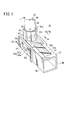
本実施の形態に係る発光装置10は、車両室内の照明に用いられ、図1及び図2に示すように、光源としての発光素子12と、前記発光素子12が実装されて平面視で長方形状に形成された基板14と、前記基板14のうち前記発光素子12が実装された面(以下、実装面と称することがある。)16に装着されて前記発光素子12に電気的に接続された電子部品18と、前記基板14に接続される一対の接続端子(ターミナル)20a、20bと、前記基板14等が収容されるケース(支持部材)22と、前記ケース22に装着されるカバー部24と、前記発光素子12から発光された光を導く導光体25とを備える。   The light emitting device 10 according to the present embodiment is used for illumination in a vehicle interior, and as shown in FIGS. 1 and 2, a light emitting element 12 serving as a light source, and a rectangular shape in plan view in which the light emitting element 12 is mounted. And a surface of the substrate 14 on which the light emitting element 12 is mounted (hereinafter, also referred to as a mounting surface) 16 and are electrically connected to the light emitting element 12. The electronic component 18, a pair of connection terminals (terminals) 20a and 20b connected to the board 14, a case (supporting member) 22 in which the board 14 and the like are housed, and a cover portion 24 attached to the case 22. And a light guide 25 that guides the light emitted from the light emitting element 12.

発光素子12としては、例えば、LEDが用いられるが、有機EL等を用いることも可能である。このようなLEDや有機ELは、公知のものを利用することができる。発光素子12は、基板14の長手方向中央よりもやや一端部側に偏在している。   As the light emitting element 12, for example, an LED is used, but it is also possible to use an organic EL or the like. Known LEDs and organic ELs can be used. The light emitting element 12 is unevenly distributed on the one end side rather than the longitudinal center of the substrate 14.

電子部品18は、発光素子12への電源の供給制御等を行うためのものであって、抵抗器やダイオード等が例示される。前記電子部品18は、基板14の短手方向の略中央であって、長手方向中央よりもやや他端部側に偏在している。   The electronic component 18 is for controlling the supply of power to the light emitting element 12, and is exemplified by a resistor and a diode. The electronic component 18 is located substantially at the center in the lateral direction of the substrate 14 and slightly unevenly located on the other end side from the center in the longitudinal direction.

基板14の長手方向に沿って電子部品18よりも他端側に近接して一対の貫通孔26a、26bが形成されている。前記貫通孔26a、26bには前記接続端子20a、20bの一端部が挿入されるものであって、その離間間隔は、任意に設定可能である。この場合、これら貫通孔26a、26bに前記接続端子20a、20bを挿入して固定した状態で、該接続端子20a、20b同士が接触しない程度の間隔が好ましい。なお、基板14の裏面28には、図示しないが、導体が面状、例えば、箔状に配設されており、発光素子12、電子部品18及び接続端子20a、20bは、前記導体を介して電気的に接続される。放熱効果を得るためである。   A pair of through holes 26a and 26b are formed along the longitudinal direction of the substrate 14 closer to the other end side than the electronic component 18. One ends of the connection terminals 20a and 20b are inserted into the through holes 26a and 26b, and the distance between them can be set arbitrarily. In this case, it is preferable that the connection terminals 20a and 20b are inserted and fixed in the through holes 26a and 26b, and the connection terminals 20a and 20b are not in contact with each other. Although not shown, conductors are arranged in a plane shape, for example, in a foil shape on the back surface 28 of the substrate 14, and the light emitting element 12, the electronic component 18, and the connection terminals 20a and 20b are connected via the conductor. It is electrically connected. This is to obtain a heat dissipation effect.

図2及び図8から諒解されるように、接続端子20aの両端面は、平坦に形成されている。但し、前記接続端子20aの両端部の形状は、特に限定されず、例えば、先細りのテーパ状に形成されていてもよい。この場合、接続端子20aの一端部を前記貫通孔26aに挿入し易くなると共に、接続端子20aの他端部を後述する電力供給用の外部コネクタに装着し易くなる。   As is clear from FIGS. 2 and 8, both end surfaces of the connection terminal 20a are formed flat. However, the shape of both ends of the connection terminal 20a is not particularly limited, and may be, for example, a tapered shape. In this case, one end of the connection terminal 20a can be easily inserted into the through hole 26a, and the other end of the connection terminal 20a can be easily attached to an external connector for power supply described later.

接続端子20aは、断面矩形状の細長い金属棒(金属板)で構成され、基板14の貫通孔26aに挿入された状態で、基板14に半田付けされる溶着部(図8参照)30と、前記溶着部30に連なる弧状の湾曲部32と、前記湾曲部32に連なり且つ他方の端部側に延伸するリード部34とを有する。   The connection terminal 20a is composed of an elongated metal rod (metal plate) having a rectangular cross section, and a welding portion (see FIG. 8) 30 that is soldered to the substrate 14 in a state of being inserted into the through hole 26a of the substrate 14, The arc-shaped curved portion 32 is connected to the welded portion 30, and the lead portion 34 is connected to the curved portion 32 and extends to the other end side.

接続端子20aの厚みT1(図8参照)は、湾曲部32を撓ませることが可能な程度の厚みに設定されている。これにより、湾曲部32を撓ませて溶着部30とリード部34との位置関係を調整することが可能となる。実際、リード部34は、図示しない電力供給用の外部コネクタに接続されるものであって、これにより、外部から発光素子12に電力を供給することができる。なお、貫通孔26bに挿入される接続端子20bは、接続端子20aと同一構成であるため、その詳細な説明を省略する。   The thickness T1 (see FIG. 8) of the connection terminal 20a is set to a thickness that allows the bending portion 32 to bend. This makes it possible to bend the bending portion 32 and adjust the positional relationship between the welding portion 30 and the lead portion 34. In fact, the lead portion 34 is connected to an external connector for power supply (not shown), which allows power to be supplied to the light emitting element 12 from the outside. Since the connection terminal 20b inserted into the through hole 26b has the same configuration as the connection terminal 20a, detailed description thereof will be omitted.

図3に示すように、ケース22は、幅広で一方向に延在し、基板14が収容されるケース本体36と、幅狭で前記ケース本体36に接続されるコネクタ部38とを有する。ケース本体36とコネクタ部38とは樹脂等で一体的に構成される。   As shown in FIG. 3, the case 22 includes a case body 36 that is wide and extends in one direction to accommodate the substrate 14, and a connector portion 38 that is narrow and connected to the case body 36. The case body 36 and the connector portion 38 are integrally formed of resin or the like.

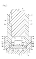
図6を参照して、ケース本体36は、平面視で略長方形状に形成された底部40と、前記底部40の短手方向の両端部に設けられた一対の第1段差部42a、42bと、前記一対の第1段差部42a、42bのそれぞれに連なる一対の第2段差部44a、44bと、前記一対の第2段差部44a、44bのそれぞれに連なる一対の側壁部46a、46bと、前記底部40に立設されて該側壁部46a、46bの上端部近傍まで延在する壁部48と、前記壁部48に対向して前記底部40に立設される分厚い壁部50とを有する。   Referring to FIG. 6, the case main body 36 includes a bottom portion 40 formed in a substantially rectangular shape in a plan view, and a pair of first step portions 42a and 42b provided at both ends in the lateral direction of the bottom portion 40. A pair of second step portions 44a, 44b connected to each of the pair of first step portions 42a, 42b, and a pair of side wall portions 46a, 46b connected to each of the pair of second step portions 44a, 44b, It has a wall portion 48 standing on the bottom portion 40 and extending to the vicinity of the upper end portions of the side wall portions 46a, 46b, and a thick wall portion 50 facing the wall portion 48 and standing on the bottom portion 40.

第1段差部42a、42bは、側壁部46a、46bに沿って延びており、その一端部が壁部48に接し、その他端部は壁部50に接している。各第1段差部42a、42bは、底部40の内面(基板14との対向面)40aに連なる第1垂直面43a、43bと、前記第1垂直面43a、43bのそれぞれに連なる第1上面45a、45bを有する。   The first step portions 42a and 42b extend along the side wall portions 46a and 46b, one end of which is in contact with the wall portion 48, and the other end is in contact with the wall portion 50. Each of the first step portions 42a, 42b has a first vertical surface 43a, 43b continuous with the inner surface 40a of the bottom portion 40 (a surface facing the substrate 14) and a first upper surface 45a continuous with the first vertical surface 43a, 43b. , 45b.

第1垂直面43a、43bの幅(第1段差部42a、42bの高さ)W1は、基板14の厚さT2と同程度の幅に設定されている。これにより、第1上面45a、45bに基板14を載置した状態で、基板14と底部40の間に適度な隙間Sが形成されることとなる。これにより、発光素子12及び電子部品18から発生した熱を該隙間Sに拡散させることができるので、基板14の裏面28全体を底部40に接触させる場合と比較して、発光素子12及び電子部品18の温度上昇を抑えることができる。   The width (height of the first step portions 42a, 42b) W1 of the first vertical surfaces 43a, 43b is set to be approximately the same as the thickness T2 of the substrate 14. As a result, an appropriate gap S is formed between the substrate 14 and the bottom portion 40 with the substrate 14 placed on the first upper surfaces 45a and 45b. As a result, the heat generated from the light emitting element 12 and the electronic component 18 can be diffused into the gap S, so that the light emitting element 12 and the electronic component 12 can be compared with the case where the entire back surface 28 of the substrate 14 is brought into contact with the bottom portion 40. The temperature rise of 18 can be suppressed.

第2段差部44a、44bは、側壁部46a、46bに沿って延びており、その一端部が壁部48に接し、その他端部はコネクタ部38に接している。各第2段差部44a、44bは、第1上面45a、45bのそれぞれに連なる第2垂直面47a、47bと、前記第2垂直面47a、47bのそれぞれに連なる第2上面49a、49bを有する。   The second step portions 44a and 44b extend along the side wall portions 46a and 46b, one end portion of which is in contact with the wall portion 48, and the other end portion thereof is in contact with the connector portion 38. Each of the second step portions 44a, 44b has a second vertical surface 47a, 47b connected to each of the first upper surfaces 45a, 45b and a second upper surface 49a, 49b connected to each of the second vertical surfaces 47a, 47b.

第2垂直面47a、47bの幅(第2段差部44a、44bの高さ)W2は、基板14の厚さT2よりも大きく設定されている。これにより、第1上面45a、45bに基板14を載置した状態で、第2上面49a、49bが基板14の実装面16よりも上方に位置することとなる。   The width (height of the second step portions 44a, 44b) W2 of the second vertical surfaces 47a, 47b is set to be larger than the thickness T2 of the substrate 14. As a result, the second upper surfaces 49a and 49b are located above the mounting surface 16 of the substrate 14 with the substrate 14 placed on the first upper surfaces 45a and 45b.

第2垂直面47a、47b同士の間隔は、基板14の短手方向の幅と略同一に設定されている。これにより、基板14の短手方向の移動を制限することができる。   The interval between the second vertical surfaces 47a and 47b is set to be substantially the same as the width of the substrate 14 in the lateral direction. Thereby, the movement of the substrate 14 in the lateral direction can be restricted.

図2に示すように、側壁部46aには所定間隔離間した複数(図では2つ)の装着孔(第2係合部)52a、52bが形成され、同様に側壁部46bにも装着孔(第2係合部)52c、52dが形成されている。装着孔52a、52bと装着孔52c、52dは、四角形状に開口し、この構成は後述するカバー部24の装着爪(第1係合部)70a、70bと、装着爪(第1係合部)70c、70dのそれぞれの形状に対応する。   As shown in FIG. 2, a plurality of (two in the figure) mounting holes (second engaging portions) 52a and 52b are formed in the side wall portion 46a at predetermined intervals, and similarly, the side wall portion 46b is also mounted with mounting holes (second engaging portions). Second engaging portions) 52c and 52d are formed. The mounting holes 52a and 52b and the mounting holes 52c and 52d are opened in a quadrangular shape, and this configuration has mounting claws (first engaging parts) 70a and 70b and a mounting claw (first engaging part) of the cover part 24 described later. ) Corresponding to the respective shapes of 70c and 70d.

装着孔52a、52bと装着孔52c、52dは、側壁部46a、46bの中央よりもやや上方に位置している。これにより、カバー部24をケース22に装着する際に、装着孔52a、52bと装着孔52c、52dのそれぞれを側壁部46a、46bの中央よりも下方に位置する場合と比較して、装着爪70a、70bと装着爪70c、70dにて外方に押される側壁部46a、46bの弾性変形量を小さくすることができるので、より小さい力で該カバー部24を該ケース22に装着することができる。   The mounting holes 52a, 52b and the mounting holes 52c, 52d are located slightly above the center of the side wall portions 46a, 46b. As a result, when the cover portion 24 is mounted on the case 22, the mounting holes 52a and 52b and the mounting holes 52c and 52d are located below the center of the side wall portions 46a and 46b, respectively. Since it is possible to reduce the amount of elastic deformation of the side walls 46a and 46b that are pushed outward by the 70a and 70b and the mounting claws 70c and 70d, it is possible to mount the cover portion 24 on the case 22 with a smaller force. it can.

また、側壁部46aの装着孔52a、52bは、ケース22の長手方向において、側壁部46aの一端から装着孔52aまでの間隔、装着孔52aと装着孔52bの間隔、及び、装着孔52bから側壁部46aの他端までの間隔が等しくなるように配置されている。側壁部46bの装着孔52cは、装着孔52aに対向しており、側壁部46bの装着孔52dは、装着孔52bに対向している。これにより、ケース22の長手方向に装着孔52a、52bと装着孔52c、52dを偏って位置する場合と比較して、該カバー部24をバランス良く保持することができる。   In addition, the mounting holes 52a and 52b of the side wall portion 46a are arranged such that, in the longitudinal direction of the case 22, the distance from one end of the side wall portion 46a to the mounting hole 52a, the distance between the mounting hole 52a and the mounting hole 52b, and the side wall from the mounting hole 52b. It is arranged so that the interval to the other end of the portion 46a is equal. The mounting hole 52c of the side wall portion 46b faces the mounting hole 52a, and the mounting hole 52d of the side wall portion 46b faces the mounting hole 52b. As a result, the cover portion 24 can be held in a well-balanced manner as compared with the case where the mounting holes 52a and 52b and the mounting holes 52c and 52d are located in a deviated position in the longitudinal direction of the case 22.

各側壁部46a、46bの外面には、装着孔52a、52bと装着孔52c、52d間に位置し、且つ、車体パネルPに設けられた後述の固定部200a、200bに係合する固定爪54a、54bがそれぞれ形成されている(図9参照)。各固定爪54a、54bは、ケース22の長手方向に沿って延在し、略直方体形状に構成された基部55a、55bと一体的に形成され、且つ、上端部から外方に向かって下傾するテーパ部57a、57bを含む。   On the outer surface of each of the side wall portions 46a and 46b, a fixing claw 54a that is located between the mounting holes 52a and 52b and the mounting holes 52c and 52d and that engages with fixing portions 200a and 200b (described later) provided on the vehicle body panel P. , 54b are respectively formed (see FIG. 9). Each of the fixing claws 54a and 54b extends along the longitudinal direction of the case 22, is integrally formed with the bases 55a and 55b having a substantially rectangular parallelepiped shape, and is inclined downward from the upper end toward the outside. It includes tapered portions 57a and 57b.

壁部48及び壁部50の高さは、ケース22にカバー部24を装着した状態で、ケース22とカバー部24とが面一になるような高さに設定されている(図1及び図8参照)。   The heights of the wall portion 48 and the wall portion 50 are set such that the case 22 and the cover portion 24 are flush with each other when the cover portion 24 is attached to the case 22 (FIGS. 1 and 2). 8).

壁部50は、平面視で略T字状に形成されており、コネクタ部38の内部迄到達する長さを有する。壁部50の上面の略中央には、長手方向に沿って延びた一対の配置溝56a、56bが形成されている(図3参照)。配置溝56a、56bの溝幅は、それぞれ上述した接続端子20a、20bのリード部34の幅と略同一の幅に設定されており、配置溝56a、56bの溝深さは、該リード部34の厚みT1と略同一の深さに設定されている(図8参照)。   The wall portion 50 is formed in a substantially T shape in a plan view and has a length reaching the inside of the connector portion 38. A pair of arrangement grooves 56a and 56b extending in the longitudinal direction are formed at approximately the center of the upper surface of the wall 50 (see FIG. 3). The groove widths of the arrangement grooves 56a and 56b are set to be substantially the same as the widths of the lead portions 34 of the connection terminals 20a and 20b described above, and the groove depths of the arrangement grooves 56a and 56b are the same as those of the lead portions 34. The thickness is set to be substantially the same as the thickness T1 (see FIG. 8).

図1から諒解されるように、コネクタ部38は、四角筒状に形成されており、その内部には、それぞれの接続端子20a、20bのリード部34が収納され、また、このコネクタ部38の筒体内部には、図示しない電力供給用の外部コネクタが挿入可能である。本実施の形態では、コネクタ部38の垂直方向の厚みはケース本体36よりも大きく形成される。コネクタ部38を構成する壁部53には、長方形状の切欠部58が形成され、前記切欠部58の幅は、後述するカバー延在部64の幅に対応している(図2参照)。   As can be seen from FIG. 1, the connector portion 38 is formed in a rectangular tube shape, and the lead portions 34 of the respective connection terminals 20a and 20b are housed inside the connector portion 38. An external connector for power supply (not shown) can be inserted into the inside of the cylinder. In the present embodiment, the vertical thickness of the connector portion 38 is formed larger than that of the case main body 36. A rectangular cutout portion 58 is formed in the wall portion 53 that constitutes the connector portion 38, and the width of the cutout portion 58 corresponds to the width of a cover extending portion 64 described later (see FIG. 2).

以上のように構成されたケース22では、底部40、第1段差部42a、42b、第2段差部44a、44b、側壁部46a、46b、壁部48、及び壁部50で囲まれた空間とコネクタ部38の切欠部58とによって、カバー部24が装着可能な空間(室)59が形成されることとなる。   In the case 22 configured as described above, a space surrounded by the bottom portion 40, the first step portions 42a and 42b, the second step portions 44a and 44b, the side wall portions 46a and 46b, the wall portion 48, and the wall portion 50. The notch 58 of the connector 38 forms a space (chamber) 59 in which the cover 24 can be mounted.

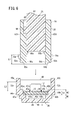
図2及び図4に示すように、カバー部24は、例えば、射出成形によって樹脂等で一体的に構成されており、平面視で略長方形状のカバー部本体60と、前記カバー部本体60の他端部から幅狭に延在するカバー延在部64と、前記カバー部本体60に形成されて導光体25を内部に装着可能な筒部80とを有する。   As shown in FIGS. 2 and 4, the cover part 24 is integrally formed of resin or the like by injection molding, for example, and has a substantially rectangular shape in plan view, and the cover part body 60. It has a cover extending portion 64 extending narrowly from the other end portion, and a tubular portion 80 formed in the cover portion main body 60 and capable of mounting the light guide 25 therein.

カバー部本体60は、その外形形状を構成するベース部61と、前記ベース部61の短手方向両端部から長手方向に沿って下方に突出した一対の突出部62a、62bと、前記一対の突出部62a、62bに形成された一対の突起部68a、68bとを有する。   The cover portion main body 60 includes a base portion 61 that forms the outer shape thereof, a pair of protruding portions 62a and 62b that protrude downward from both ends in the lateral direction of the base portion 61 along the longitudinal direction, and the pair of protruding portions. It has a pair of protrusions 68a and 68b formed on the portions 62a and 62b.

前記突出部62a、62bの突出量は、上述した側壁部46a、46bの高さに対応して規定される。突起部68a、68bの長さは、突出部62a、62bの長さと同一に設定され、その突出量は、上述した第2垂直面47a、47bの幅W2と基板14の厚さT2の差(W2−T2)と同程度に設定されている(図6参照)。   The amount of protrusion of the protrusions 62a and 62b is defined according to the height of the side wall portions 46a and 46b described above. The lengths of the protrusions 68a and 68b are set to be the same as the lengths of the protrusions 62a and 62b, and the protrusion amount is the difference between the width W2 of the second vertical surfaces 47a and 47b and the thickness T2 of the substrate 14 ( W2-T2) and is set to the same level (see FIG. 6).

各突出部62a、62bの外側面には、上述した装着孔52a、52bと装着孔52c、52dに嵌合可能な装着爪70a、70bと装着爪70c、70dがそれぞれ互いに離間して設けられ、その離間間隔は、上述した装着孔52a、52bと装着孔52c、52dの離間間隔と同一に設定されている。装着爪70a、70b、70c、70dは、略直方体状であるが、その下端部は下方に向かうに従って徐々に先細りするテーパ状に形成されている。   Mounting claws 70a, 70b and mounting claws 70c, 70d that can be fitted into the above-described mounting holes 52a, 52b and mounting holes 52c, 52d are provided separately from each other on the outer surface of each of the projecting portions 62a, 62b, The spacing is set to be the same as the spacing between the mounting holes 52a and 52b and the mounting holes 52c and 52d described above. The mounting claws 70a, 70b, 70c, 70d have a substantially rectangular parallelepiped shape, but the lower end portion thereof is formed in a tapered shape that gradually tapers downward.

この場合、本実施の形態では、図6に示すように、突起部68a、68bの下端面69a、69bから装着爪70a、70bと装着爪70c、70dの上端面までの距離L1は、ケース本体36の第1上面45a、45bに基板14を載置した状態において、基板14の実装面16から装着孔52a、52bと装着孔52c、52dの上端部までの距離L2よりも若干大きく設定されている。その理由については後述する。   In this case, in the present embodiment, as shown in FIG. 6, the distance L1 from the lower end surfaces 69a and 69b of the protrusions 68a and 68b to the upper ends of the mounting claws 70a and 70b and the mounting claws 70c and 70d is the case body. In a state where the board 14 is placed on the first upper surfaces 45a and 45b of 36, the distance L2 from the mounting surface 16 of the board 14 to the upper ends of the mounting holes 52a and 52b and the mounting holes 52c and 52d is set to be slightly larger than the distance L2. There is. The reason will be described later.

ベース部61とカバー延在部64の境界部には、下方に突出した端子保持部72が形成されている(図4参照)。端子保持部72の下端面73と突起部68a、68bの下端面69a、69bとは、それぞれが一体に接続して平坦面を形成している。   A terminal holding portion 72 protruding downward is formed at a boundary portion between the base portion 61 and the cover extending portion 64 (see FIG. 4). The lower end surface 73 of the terminal holding portion 72 and the lower end surfaces 69a and 69b of the protrusions 68a and 68b are integrally connected to each other to form a flat surface.

端子保持部72の下端面73には、一対の凹部74a、74bがカバー部本体60の短手方向に所定間隔離間して形成され、その離間間隔は、上述した壁部50に設けられた配置溝56a、56bの離間間隔に対応している。   A pair of concave portions 74a and 74b are formed on the lower end surface 73 of the terminal holding portion 72 at a predetermined interval in the lateral direction of the cover body 60, and the distance between the recesses 74a and 74b is provided in the wall portion 50 described above. It corresponds to the spacing between the grooves 56a and 56b.

カバー延在部64の下面のうち端子保持部72に隣接する部位には、前記電力供給用の外部コネクタを保持するための溝76が形成されている。   A groove 76 for holding the external connector for power supply is formed in a portion of the lower surface of the cover extending portion 64 adjacent to the terminal holding portion 72.

筒部80は、略円筒状であってベース部61の一端部側に位置しており、筒部80の内部(内孔)は、ベース部61の下端面に開口している。筒部80には、その周方向に沿って4つの肉厚部位82a、82b、82c、82dが互いに離間して形成されている。なお、各肉厚部位82a、82b、82c、82dは、筒部80の軸線方向全体に亘って延在しており、その筒部80の周方向に沿った長さは略同一に設定されている。   The tubular portion 80 has a substantially cylindrical shape and is located on one end side of the base portion 61, and the inside (inner hole) of the tubular portion 80 is open to the lower end surface of the base portion 61. Four thick portions 82a, 82b, 82c, 82d are formed on the cylindrical portion 80 so as to be spaced from each other along the circumferential direction. Each of the thick portions 82a, 82b, 82c, 82d extends over the entire axial direction of the tubular portion 80, and the lengths of the tubular portion 80 along the circumferential direction are set to be substantially the same. There is.

肉厚部位82aと肉厚部位82cは、ベース部61の長手方向に沿って並んでおり、肉厚部位82bと肉厚部位82dは、ベース部61の短手方向に沿って並んでいる。   The thick portion 82a and the thick portion 82c are arranged along the longitudinal direction of the base portion 61, and the thick portion 82b and the thick portion 82d are arranged along the lateral direction of the base portion 61.

図6に示すように、肉厚部位82bの内周面の下端部には第1ストッパ部86aが形成され、肉厚部位82dの内周面の下端部には前記第1ストッパ部86aに対向して第1ストッパ部86bが形成されている。また、肉厚部位82bの内周面の上端側には、筒部80の軸線方向に延在して該筒部80の上端面に開口した係止溝88が形成されている。なお、係止溝88は、筒部80の上端面に開口していなくてもよい。つまり、係止溝88の上端部は、筒部80の上端面よりもやや下方に位置していても構わない。各第1ストッパ部86a、86bは、略直方体状に形成され、その上端面は平坦に形成されている。   As shown in FIG. 6, a first stopper portion 86a is formed at the lower end of the inner peripheral surface of the thick portion 82b, and a first stopper portion 86a is formed at the lower end of the inner peripheral surface of the thick portion 82d so as to face the first stopper portion 86a. Then, the first stopper portion 86b is formed. Further, on the upper end side of the inner peripheral surface of the thick portion 82b, a locking groove 88 is formed which extends in the axial direction of the tubular portion 80 and is open to the upper end surface of the tubular portion 80. The locking groove 88 does not have to be opened in the upper end surface of the tubular portion 80. That is, the upper end portion of the locking groove 88 may be located slightly below the upper end surface of the tubular portion 80. Each of the first stopper portions 86a and 86b is formed in a substantially rectangular parallelepiped shape, and the upper end surface thereof is formed flat.

図5に示すように、肉厚部位82aの内周面には、筒部80の軸線方向に沿って延びた溝部90aが形成され、その溝部90aは、筒部80の上端よりもやや下方の位置からその下端まで延在している。これにより、肉厚部位82aの内周面の上端部に後述する導光体25の凸部96aが当接(係止)可能な第2ストッパ部92aが形成されることとなる。   As shown in FIG. 5, a groove portion 90a extending along the axial direction of the tubular portion 80 is formed on the inner peripheral surface of the thick portion 82a, and the groove portion 90a is located slightly below the upper end of the tubular portion 80. It extends from the position to its lower edge. As a result, the second stopper portion 92a is formed at the upper end of the inner peripheral surface of the thick portion 82a, with which the convex portion 96a of the light guide 25, which will be described later, can abut (lock).

肉厚部位82cの内周面には、前記溝部90aと同一形状の溝部90bが該溝部90aに対向して形成されている。これにより、肉厚部位82cの内周面の上端部に後述する導光体25の凸部96bが当接(係止)可能な第2ストッパ部92bが形成されることとなる。なお、第2ストッパ部92a、92bのそれぞれは、上端に向かうに従って先細りのテーパ状に形成され、その下端面は平坦に形成されている。   A groove portion 90b having the same shape as the groove portion 90a is formed on the inner peripheral surface of the thick portion 82c so as to face the groove portion 90a. As a result, the second stopper portion 92b with which the convex portion 96b of the light guide 25 described later can abut (lock) is formed at the upper end portion of the inner peripheral surface of the thick portion 82c. Each of the second stopper portions 92a and 92b is formed in a taper shape that tapers toward the upper end, and the lower end surface thereof is formed flat.

導光体25は、透明体であって、樹脂材料で一体的に構成されている。また、図2、図5、及び、図6に示すように、導光体25は、円柱状に形成された導光体本体94と、前記導光体本体94の外周面に形成されて上述した一対の溝部90a、90bのそれぞれに挿入可能な一対の凸部96a、96bと、前記導光体本体94の外周面に形成されて該導光体本体94の軸線方向に延びた略直方体状の係止用突起98とを有する。   The light guide 25 is a transparent body and is integrally formed of a resin material. In addition, as shown in FIGS. 2, 5, and 6, the light guide 25 is formed on the light guide body 94 formed in a columnar shape, and on the outer peripheral surface of the light guide body 94. A pair of convex portions 96a and 96b that can be inserted into the pair of groove portions 90a and 90b, respectively, and a substantially rectangular parallelepiped shape that is formed on the outer peripheral surface of the light guide body 94 and extends in the axial direction of the light guide body 94. Locking projection 98.

導光体本体94の外径は、筒部80の内径に対応している。各凸部96a、96bは、略直方体状であるが、その下端部は下方に向かうに従って徐々に先細りするテーパ状に形成され、その上端面は平坦に形成されている。また、各凸部96a、96bは、溝部90a、90bに挿入可能な大きさに設定される。   The outer diameter of the light guide body 94 corresponds to the inner diameter of the tubular portion 80. Each of the convex portions 96a and 96b has a substantially rectangular parallelepiped shape, but the lower end portion thereof is formed in a taper shape that gradually tapers downward, and the upper end surface thereof is formed flat. Further, each of the convex portions 96a and 96b is set to a size that can be inserted into the groove portions 90a and 90b.

なお、導光体本体94の下端面から凸部96a、96bの上端面までの距離L3は、第1ストッパ部86a、86bの上端面から第2ストッパ部92a、92bの下端面までの距離L4と略同一の長さに設定されている。この理由は後述する。   The distance L3 from the lower end surface of the light guide body 94 to the upper end surfaces of the convex portions 96a and 96b is the distance L4 from the upper end surfaces of the first stopper portions 86a and 86b to the lower end surfaces of the second stopper portions 92a and 92b. And the length is set to be almost the same. The reason for this will be described later.

係止用突起98の幅(導光体本体94の軸線方向及び半径方向に直交する方向に沿った長さ)は、上述した係止溝88の溝幅と略同一に設定されている。これにより、係止用突起98を係止溝88に挿入した状態で、前記係止用突起98が前記係止溝88の一対の溝側面のそれぞれに接触するので、筒部80の周方向において導光体25を筒部80に確実に位置決めすることができる。よって、筒部80に対する導光体25の誤組を防止することができる。また、導光体25を筒部80の内部に装着した状態で、該導光体25が筒部80の周方向に回転することを好適に防止することができる。   The width of the locking projection 98 (the length along the direction orthogonal to the axial direction and the radial direction of the light guide body 94) is set to be substantially the same as the groove width of the locking groove 88 described above. As a result, in a state where the locking projection 98 is inserted into the locking groove 88, the locking projection 98 comes into contact with each of the pair of groove side surfaces of the locking groove 88, so that in the circumferential direction of the tubular portion 80. The light guide 25 can be reliably positioned in the tubular portion 80. Therefore, it is possible to prevent erroneous assembly of the light guide 25 with respect to the tubular portion 80. Further, it is possible to preferably prevent the light guide 25 from rotating in the circumferential direction of the cylinder 80 in a state where the light guide 25 is mounted inside the cylinder 80.

次に、本実施形態に係る発光装置10を組み立てる手順について説明する。先ず、基板14の一方の面(実装面16)に発光素子12と電子部品18をそれぞれ実装すると共に、基板14の貫通孔26a、26bに接続端子20a、20bのそれぞれの溶着部30を挿入し、該溶着部30を半田付けにより基板14に固定する。   Next, a procedure for assembling the light emitting device 10 according to the present embodiment will be described. First, the light emitting element 12 and the electronic component 18 are mounted on one surface (mounting surface 16) of the board 14, and the welding portions 30 of the connection terminals 20a and 20b are inserted into the through holes 26a and 26b of the board 14, respectively. The welded portion 30 is fixed to the substrate 14 by soldering.

その後、前記発光素子12等が実装された基板14をケース22内に進入させる。このとき、図6に示すように、基板14の裏面28が第1上面45a、45bに接触すると共に、基板14の側面が第2垂直面47a、47bに接触し、壁部50の配置溝56a、56b内に接続端子20a、20bのそれぞれのリード部34が収納されることとなる。これにより、基板14と接続端子20a、20bがケース22内に位置決めされる。   After that, the substrate 14 on which the light emitting device 12 and the like are mounted is inserted into the case 22. At this time, as shown in FIG. 6, the back surface 28 of the substrate 14 contacts the first upper surfaces 45a and 45b, the side surface of the substrate 14 contacts the second vertical surfaces 47a and 47b, and the arrangement groove 56a of the wall portion 50 is formed. , 56b, the lead portions 34 of the connection terminals 20a, 20b are housed. As a result, the board 14 and the connection terminals 20a and 20b are positioned in the case 22.

また、導光体25を筒部80の内部に装着する。具体的には、図5に示すように、係止用突起98が係止溝88に挿入されるようにカバー部24に対する導光体25の向きを調節した上で、該導光体25を筒部80の内部に進入させる。そうすると、導光体本体94の外周面と筒部80の内周面とが接触した状態で、凸部96a、96bのテーパ面が第2ストッパ部92a、92bのテーパ面に接触するに至る。   Further, the light guide 25 is mounted inside the tubular portion 80. Specifically, as shown in FIG. 5, after adjusting the direction of the light guide 25 with respect to the cover portion 24 so that the locking projection 98 is inserted into the locking groove 88, the light guide 25 is fixed. It is made to enter the inside of the tubular portion 80. Then, in a state where the outer peripheral surface of the light guide body 94 and the inner peripheral surface of the tubular portion 80 are in contact with each other, the tapered surfaces of the convex portions 96a and 96b come into contact with the tapered surfaces of the second stopper portions 92a and 92b.

続いて、導光体25をベース部61が位置する側に押圧すると、肉厚部位82a、82cが互いに離間する方向(筒部80の半径方向外方)に弾性変形しながら導光体25が筒部80の内部にさらに進入し、導光体本体94の下端面が第1ストッパ部86a、86bの上端面に当接することとなる。このとき、弾性変形していた肉厚部位82a、82cは原形に復帰し、係止用突起98は係止溝88に配置され、凸部96a、96bは溝部90a、90bに配置される。   Subsequently, when the light guide 25 is pressed toward the side where the base portion 61 is located, the light guide 25 is elastically deformed in a direction in which the thick portions 82a and 82c are separated from each other (outward in the radial direction of the tubular portion 80). Further, the lower end surface of the light guide main body 94 comes into contact with the upper end surfaces of the first stopper portions 86a and 86b by further entering the inside of the tubular portion 80. At this time, the elastically deformed thick portions 82a and 82c return to the original shape, the locking projection 98 is arranged in the locking groove 88, and the convex portions 96a and 96b are arranged in the groove portions 90a and 90b.

なお、上述したように、導光体本体94の下端面から凸部96a、96bの上端面までの距離L3が第1ストッパ部86a、86bの上端面から第2ストッパ部92a、92bの下端面までの距離L4と略同一に設定されているので、この状態において、凸部96aの上端面が第2ストッパ部92aの下端面に当接すると共に凸部96bの上端面が第2ストッパ部92bの下端面に当接する。その結果、導光体25は、筒部80の内部に位置決め保持される(図6参照)。なお、このとき、導光体本体94の一部は、筒部80から突出している。   Note that, as described above, the distance L3 from the lower end surface of the light guide body 94 to the upper end surfaces of the protrusions 96a and 96b is determined from the upper end surfaces of the first stopper portions 86a and 86b to the lower end surfaces of the second stopper portions 92a and 92b. Since it is set to be substantially the same as the distance L4 up to, the upper end surface of the convex portion 96a contacts the lower end surface of the second stopper portion 92a and the upper end surface of the convex portion 96b corresponds to the second stopper portion 92b in this state. Abut on the lower end surface. As a result, the light guide 25 is positioned and held inside the tubular portion 80 (see FIG. 6). At this time, a part of the light guide body 94 projects from the tubular portion 80.

続いて、カバー部24をケース22に装着する。具体的には、カバー部24をケース22に近接すると、カバー部24の突出部62a、62bの外側面とケース本体36の側壁部46a、46bの内面とが互いに接触した状態で突出部62a、62bの下端がケース本体36内に進入し、このため装着爪70a、70bと、装着爪70c、70dが側壁部46a、46bに接触するに至る。   Then, the cover portion 24 is attached to the case 22. Specifically, when the cover portion 24 approaches the case 22, the protruding portions 62a and 62b of the cover portion 24 and the inner surfaces of the side wall portions 46a and 46b of the case main body 36 are in contact with each other and the protruding portion 62a, The lower end of 62b enters the case main body 36, so that the mounting claws 70a, 70b and the mounting claws 70c, 70d come into contact with the side wall portions 46a, 46b.

そして、カバー部24をケース本体36の底部40側に押圧すると、側壁部46a、46bが互いに離間する方向に弾性変形すると共に、その反力で突出部62a、62bが互いに近接する方向に弾性変形しながら、突出部62a、62bがケース本体36内にさらに進入する。   When the cover portion 24 is pressed toward the bottom portion 40 of the case main body 36, the side walls 46a and 46b are elastically deformed in the direction of separating from each other, and the reaction force elastically deforms the protrusions 62a and 62b in the direction of approaching each other. Meanwhile, the protrusions 62a and 62b further enter into the case body 36.

その後、突起部68a、68bの下端面69a、69bが基板14の実装面16に接触すると共に、突出部62a、62bの下端面が第2上面49a、49bに接触することとなる。なお、上述したように、下端面69a、69bから装着爪70a、70bと装着爪70c、70dの上端面までの距離L1が実装面16から装着孔52a、52b、と装着孔52c、52dの上端部までの距離L2よりも大きく設定されているため、この状態において、装着爪70a、70b、70c、70dは未だ装着孔52a、52b、52c、52dに嵌合していない。   Then, the lower end surfaces 69a and 69b of the protrusions 68a and 68b contact the mounting surface 16 of the substrate 14, and the lower end surfaces of the protrusions 62a and 62b contact the second upper surfaces 49a and 49b. As described above, the distance L1 from the lower end surfaces 69a, 69b to the upper ends of the mounting claws 70a, 70b and the mounting claws 70c, 70d is determined by the mounting surface 16 to the upper ends of the mounting holes 52a, 52b and the mounting holes 52c, 52d. Since it is set to be larger than the distance L2 to the portion, in this state, the mounting claws 70a, 70b, 70c, 70d are not yet fitted in the mounting holes 52a, 52b, 52c, 52d.

次いで、カバー部24を底部40側にさらに押し込むと、ケース本体36及びカバー部24が若干撓むので、カバー部24がケース本体36内にさらに進入し、装着爪70a、70b、70c、70dが装着孔52a、52b、52c、52dに嵌合することとなる(図6参照)。このとき、弾性変形していた突出部62a、62b及び側壁部46a、46bは原形に復帰する。その結果、カバー部24は、突起部68a、68bの下端面69a、69bで基板14の実装面16を押圧した(実装面16に当接した)状態でケース22に装着される。このとき、端子保持部72の下端面73は、接続端子20a、20bのそれぞれのリード部34に当接することとなる(図8参照)。   Then, when the cover portion 24 is further pushed into the bottom portion 40 side, the case body 36 and the cover portion 24 are slightly bent, so that the cover portion 24 further enters the case body 36 and the mounting claws 70a, 70b, 70c, 70d are removed. It will be fitted in the mounting holes 52a, 52b, 52c, 52d (see FIG. 6). At this time, the elastically deformed protrusions 62a and 62b and the side wall portions 46a and 46b are restored to their original shapes. As a result, the cover portion 24 is attached to the case 22 in a state in which the mounting surface 16 of the substrate 14 is pressed (contacted with the mounting surface 16) by the lower end surfaces 69a and 69b of the protrusions 68a and 68b. At this time, the lower end surface 73 of the terminal holding portion 72 comes into contact with the respective lead portions 34 of the connection terminals 20a and 20b (see FIG. 8).

以上のようにして組み立てられた発光装置10は、図9に示すように、図示しない車両の車体パネルPの所定の位置に配設される。具体的には、筒部80における基板14が位置する側とは反対側の開口部が鉛直下方に指向すると共に、車体パネルPに形成された窓部Hと導光体本体94とが対向するように車体パネルPの裏面側(図9の二点鎖線の位置)に発光装置10をセットし、該発光装置10を車体パネルPに接近させる。これにより、先ず、車体パネルPの裏面側に設けられた樹脂製の固定部200a、200bが発光装置10の固定爪54a、54bのテーパ部57a、57bに接触する。   The light emitting device 10 assembled as described above is arranged at a predetermined position of a vehicle body panel P of a vehicle (not shown) as shown in FIG. Specifically, the opening of the tubular portion 80 on the side opposite to the side on which the substrate 14 is located is directed vertically downward, and the window H formed in the vehicle body panel P and the light guide body 94 face each other. As described above, the light emitting device 10 is set on the back surface side of the vehicle body panel P (the position of the chain double-dashed line in FIG. 9), and the light emitting device 10 is brought close to the vehicle body panel P. As a result, first, the resin-made fixing portions 200a and 200b provided on the back surface side of the vehicle body panel P come into contact with the tapered portions 57a and 57b of the fixing claws 54a and 54b of the light emitting device 10.

次いで、発光装置10をさらに車体パネルP側に押圧すると、固定部200a、200bが互いに離間する方向に弾性変形しながら、発光装置10が車体パネルP側に進行し、筒部80が車体パネルPの裏面に当接すると共に導光体本体94の一部が窓部Hに嵌まり込むと共に車両室内に露出する。このとき、弾性変形していた固定部200a、200bは原形に復帰する。その結果、発光装置10は、車体パネルPと固定部200a、200bによって挟圧されるので、車体パネルPに対してしっかりと固定される。   Next, when the light emitting device 10 is further pressed toward the vehicle body panel P, the light emitting device 10 advances toward the vehicle body panel P side while the fixing portions 200a and 200b are elastically deformed in the direction in which the fixing portions 200a and 200b are separated from each other, and the tubular portion 80 moves toward the vehicle body panel P. While being in contact with the back surface of the light guide body 94, a part of the light guide body 94 is fitted into the window portion H and is exposed in the vehicle compartment. At this time, the elastically deformed fixing portions 200a and 200b return to the original shape. As a result, the light emitting device 10 is pinched by the vehicle body panel P and the fixing portions 200a and 200b, so that the light emitting device 10 is firmly fixed to the vehicle body panel P.

本実施の形態に係る発光装置10によれば、ケース本体36の第1上面45a、45bに基板14の裏面28を当接させた状態でカバー部24の突起部68a、68bの下端面69a、69bを基板14の実装面16に押し付けて(圧接させて)いるので、ケース22に対して基板14を確実に保持することができる。これにより、発光素子12と筒部80の間隔を一定にすることができる。   According to the light emitting device 10 according to the present embodiment, the lower end surfaces 69a of the protrusions 68a and 68b of the cover portion 24 in the state where the back surface 28 of the substrate 14 is in contact with the first upper surfaces 45a and 45b of the case body 36, Since 69b is pressed (pressed against) the mounting surface 16 of the substrate 14, the substrate 14 can be reliably held with respect to the case 22. Thereby, the distance between the light emitting element 12 and the tubular portion 80 can be made constant.

また、導光体25を筒部80の内部に装着した状態で導光体本体94の下端面が第1ストッパ部86a、86bの上端面に当接しているので、導光体25の基板14に向かう側の移動が阻止される。これにより、導光体25が筒部80の内部に位置決めされる。   Further, since the lower end surface of the light guide body 94 is in contact with the upper end surfaces of the first stopper portions 86a and 86b in a state where the light guide body 25 is mounted inside the tubular portion 80, the substrate 14 of the light guide body 25 is provided. The movement toward the side is blocked. As a result, the light guide 25 is positioned inside the tubular portion 80.

さらに、この状態で、凸部96a、96bの上端面が第2ストッパ部92a、92bの下端面に当接しているので、導光体25における基板14が位置する側とは反対側の移動が阻止される。これにより、例えば、筒部80における基板14が位置する側とは反対側の開口部が鉛直下方に指向するように発光装置10の向きを設定した場合であっても、筒部80に対する導光体25の位置がずれることはない。これにより、発光装置10の向きによらず、発光素子12と導光体25の距離を一定に保持することができる。   Furthermore, in this state, since the upper end surfaces of the convex portions 96a and 96b are in contact with the lower end surfaces of the second stopper portions 92a and 92b, the movement of the light guide 25 on the side opposite to the side on which the substrate 14 is located can be prevented. Be blocked. Thereby, for example, even when the orientation of the light emitting device 10 is set so that the opening of the tubular portion 80 on the side opposite to the side where the substrate 14 is located is directed vertically downward, the light guide to the tubular portion 80 is performed. The position of the body 25 does not shift. As a result, the distance between the light emitting element 12 and the light guide 25 can be kept constant regardless of the orientation of the light emitting device 10.

本実施の形態では、第1ストッパ部86a、86bと第2ストッパ部92a、92bを利用して導光体25を筒部80の内部に位置決め保持しているので、筒部80の壁部に前記導光体25を保持するための孔を形成する必要がない。そのため、発光素子12から発光された光が該孔を介して外部に漏れるような問題も起きない。よって、部品点数の増加を招くことなく発光装置10の品質を向上させることができる。   In the present embodiment, the light guide 25 is positioned and held inside the tubular portion 80 by using the first stopper portions 86a and 86b and the second stopper portions 92a and 92b, so that the wall portion of the tubular portion 80 is held. It is not necessary to form a hole for holding the light guide 25. Therefore, there is no problem that the light emitted from the light emitting element 12 leaks to the outside through the hole. Therefore, the quality of the light emitting device 10 can be improved without increasing the number of components.

本実施の形態では、第2ストッパ部92a、92bに当接可能な凸部96a、96bを導光体本体94の外面に一体的に形成しているので、導光体25を筒部80の内部に挿入する際に、前記凸部96a、96bを前記第2ストッパ部92a、92bに押し当てて肉厚部位82a、82cを筒部80の半径方向外方に撓ませることができる。これにより、前記導光体25を前記筒部80の内部に一層容易に挿入することができる。   In the present embodiment, since the convex portions 96a and 96b capable of contacting the second stopper portions 92a and 92b are integrally formed on the outer surface of the light guide body 94, the light guide 25 is fixed to the tubular portion 80. When inserted inside, the convex portions 96a and 96b can be pressed against the second stopper portions 92a and 92b to bend the thick portions 82a and 82c outward in the radial direction of the tubular portion 80. Thereby, the light guide 25 can be inserted into the cylindrical portion 80 more easily.

また、導光体25の凸部96a、96bのテーパ面を第2ストッパ部92a、92bのテーパ面に接触させた状態で導光体25をベース部61側に押圧しているので、肉厚部位82a、82cを筒部80の半径方向外方に容易に撓ませることができる。従って、導光体25を筒部80の内部にさらに容易に挿入することができる。   In addition, since the light guide 25 is pressed toward the base 61 while the tapered surfaces of the convex portions 96a and 96b of the light guide 25 are in contact with the tapered surfaces of the second stoppers 92a and 92b, the thickness is increased. The parts 82a and 82c can be easily bent outward in the radial direction of the tubular portion 80. Therefore, the light guide 25 can be inserted into the cylindrical portion 80 more easily.

さらに、一対の第1ストッパ部86a、86bをベース部61の短手方向に対向して配置すると共に、一対の第2ストッパ部92a、92bをベース部61の長手方向に対向して配置しているので、例えば、第1ストッパ部86a及び第2ストッパ部92aを1つずつ設けた場合(第1ストッパ部86b及び第2ストッパ部92bを省略した場合)と比較して導光体25を筒部80にバランス良く位置決め保持することができる。また、カバー部24を射出成形により成形する場合に、筒部80の内部に配置される中子を適当な大きさに分割することで、該中子を該筒部80の内部から容易に取り出すことができる。   Further, the pair of first stopper portions 86a and 86b are arranged to face each other in the lateral direction of the base portion 61, and the pair of second stopper portions 92a and 92b are arranged to face each other in the longitudinal direction of the base portion 61. Therefore, for example, as compared with the case where the first stopper portion 86a and the second stopper portion 92a are provided one by one (the first stopper portion 86b and the second stopper portion 92b are omitted), The portion 80 can be positioned and held with good balance. Further, when the cover portion 24 is molded by injection molding, the core arranged inside the tubular portion 80 is divided into appropriate sizes, so that the core can be easily taken out from the inside of the tubular portion 80. be able to.

本実施の形態に係る発光装置10によれば、カバー部24の一対の突出部62a、62bが発光素子12を挟むようにして基板14の実装面16を押圧すると共に、前記突出部62a、62bのそれぞれに設けられた装着爪70a、70bと装着爪70c、70dが、側壁部46a、46bのそれぞれに形成された装着孔52a、52bと装着孔52c、52dに嵌合するので、発光素子12と筒部80の間隔を一定に保持することができる。   According to the light emitting device 10 of the present embodiment, the pair of protrusions 62a and 62b of the cover portion 24 presses the mounting surface 16 of the substrate 14 so as to sandwich the light emitting element 12, and the protrusions 62a and 62b respectively. Since the mounting claws 70a, 70b and the mounting claws 70c, 70d provided on the above are fitted into the mounting holes 52a, 52b and the mounting holes 52c, 52d formed in the side wall portions 46a, 46b, respectively, the light emitting element 12 and the cylinder The interval between the parts 80 can be kept constant.

また、本実施の形態では、カバー部24をケース22に装着した状態で、カバー部24の突起部68a、68bの外側面がケース本体36の第2垂直面47a、47bに接触しているので、カバー部24と基板14がその短手方向に相対移動することを好適に抑えることができる。これにより、発光素子12の光軸を筒部80の軸線上に位置させることができる。   Further, in the present embodiment, the outer surfaces of the protrusions 68a and 68b of the cover portion 24 are in contact with the second vertical surfaces 47a and 47b of the case body 36 when the cover portion 24 is attached to the case 22. The relative movement of the cover portion 24 and the substrate 14 in the lateral direction can be appropriately suppressed. Thereby, the optical axis of the light emitting element 12 can be located on the axis of the tubular portion 80.

さらにまた、本実施の形態では、端子保持部72の下端面73が配置溝56a、56bに収納された接続端子20a、20bのそれぞれのリード部34に当接しているので、接続端子20a、20bをケース22に対して好適に保持することができる。   Furthermore, in the present embodiment, since the lower end surface 73 of the terminal holding portion 72 is in contact with the respective lead portions 34 of the connection terminals 20a and 20b housed in the arrangement grooves 56a and 56b, the connection terminals 20a and 20b are provided. Can be suitably held with respect to the case 22.

これにより、接続端子20a、20bを保持するための部品を設ける必要がないので、発光装置10全体を有効に小型化及び軽量化することができる。また、接続端子20a、20bのそれぞれは、溶着部30を介して基板14に固定されているので、該接続端子20a、20bを保持することにより、基板14の保持が一層安定する。   Accordingly, it is not necessary to provide a component for holding the connection terminals 20a and 20b, so that the entire light emitting device 10 can be effectively reduced in size and weight. Further, since each of the connection terminals 20a and 20b is fixed to the substrate 14 via the welded portion 30, holding the connection terminals 20a and 20b further stabilizes the holding of the substrate 14.

ところで、通常、ケース22には寸法公差がある。そのため、発光素子12や接続端子20a、20b等が実装された基板14をケース22内に位置決めした際に、例えば、接続端子20a、20bの各リード部34が配置溝56a、56bから若干浮き出ることがある。   By the way, the case 22 usually has a dimensional tolerance. Therefore, when the substrate 14 on which the light emitting element 12 and the connection terminals 20a and 20b are mounted is positioned in the case 22, for example, the lead portions 34 of the connection terminals 20a and 20b slightly protrude from the arrangement grooves 56a and 56b. There is.

このような場合であっても、本実施の形態に係る発光装置10によれば、接続端子20a、20bのそれぞれに湾曲部32を設けているので、カバー部24をケース22に装着した際に、湾曲部32を撓ませることにより、溶着部30に余計な応力をかけることなく、接続端子20a、20bを保持することが可能となる。これにより、溶着部30の接続不良を好適に抑えることができる。   Even in such a case, according to the light emitting device 10 according to the present embodiment, since the curved portions 32 are provided on each of the connection terminals 20a and 20b, when the cover portion 24 is attached to the case 22. By bending the bending portion 32, it is possible to hold the connection terminals 20a and 20b without applying extra stress to the welding portion 30. Thereby, the poor connection of the welded portion 30 can be suppressed appropriately.

また、端子保持部72の下端面73に一対の凹部74a、74bを形成しているので、接続端子20a、20bの湾曲部32がカバー部24に当たり、該カバー部24をケース22に装着し難くなることを防止することができる。さらに、端子保持部72の下端面73に一対の凹部74a、74bを形成せずに、前記湾曲部32と該下端面73の間に該湾曲部32が該下端面73に当たらないように空間を設ける場合と比較して、発光装置10全体をコンパクトにすることができる。   Further, since the pair of recesses 74a and 74b are formed on the lower end surface 73 of the terminal holding portion 72, the curved portions 32 of the connection terminals 20a and 20b hit the cover portion 24, and it is difficult to attach the cover portion 24 to the case 22. Can be prevented. Further, a space is formed between the curved portion 32 and the lower end surface 73 so that the curved portion 32 does not hit the lower end surface 73 without forming a pair of recesses 74a and 74b on the lower end surface 73 of the terminal holding portion 72. The entire light emitting device 10 can be made compact as compared with the case where the light emitting device 10 is provided.

さらに、本実施の形態では、発光素子12が実装される基板14の実装面16に電子部品18を配設しているので、電子部品18を基板14の裏面28に実装する場合と比較して、発光装置10全体を好適に小型化及び軽量化することができる。   Further, in the present embodiment, since the electronic component 18 is arranged on the mounting surface 16 of the substrate 14 on which the light emitting element 12 is mounted, compared with the case where the electronic component 18 is mounted on the back surface 28 of the substrate 14. Therefore, the entire light emitting device 10 can be suitably reduced in size and weight.

本実施の形態に係る発光装置10において、カバー部24及び導光体25に代え、図10及び図11に示すようなカバー部100及び導光体102を用いてもよい。この変形例において、上記実施形態の構成要素と同一の構成要素には同一の参照符号を付し、詳細な説明を省略する。   In the light emitting device 10 according to the present embodiment, the cover part 100 and the light guide body 102 as shown in FIGS. 10 and 11 may be used instead of the cover part 24 and the light guide body 25. In this modification, the same components as those of the above embodiment are designated by the same reference numerals, and detailed description thereof will be omitted.

図10及び図11に示すように、カバー部100は、筒部104の構成が上述した筒部80と異なる。具体的には、上述した肉厚部位82aの溝部90aを省略して肉厚部位82aの内周面の上端に第2ストッパ部106aを突設すると共に、肉厚部位82cの溝部90bを省略して肉厚部位82cの内周面の上端に第2ストッパ部106bを突設している。なお、各第2ストッパ部106a、106bは、上端に向かうに従って徐々に先細りするテーパ状に形成されている。   As shown in FIGS. 10 and 11, the cover portion 100 is different in the configuration of the tubular portion 104 from the above-described tubular portion 80. Specifically, the groove portion 90a of the thick portion 82a is omitted, the second stopper portion 106a is provided at the upper end of the inner peripheral surface of the thick portion 82a, and the groove portion 90b of the thick portion 82c is omitted. A second stopper portion 106b is provided at the upper end of the inner peripheral surface of the thick portion 82c. Note that each of the second stopper portions 106a and 106b is formed in a tapered shape that gradually tapers toward the upper end.

筒部104では、上述した実施の形態と同様に、肉厚部位82bの内周面の下端部に第1ストッパ部86aが形成され、肉厚部位82dの内周面の下端部に第1ストッパ部86bが形成されている。また、導光体102では、上述した導光体25の凸部96a、96bが省略されている。   In the cylindrical portion 104, as in the above-described embodiment, the first stopper portion 86a is formed at the lower end portion of the inner peripheral surface of the thick portion 82b, and the first stopper portion 86a is formed at the lower end portion of the inner peripheral surface of the thick portion 82d. The portion 86b is formed. Further, in the light guide body 102, the convex portions 96a and 96b of the light guide body 25 described above are omitted.

この場合、導光体102を筒部104の内部に装着した状態で、導光体本体94の下端面が第1ストッパ部86a、86bの上端面に当接すると共に導光体本体94の上端面が第2ストッパ部106a、106bの下端面に当接することにより、導光体102が筒部104の内部に位置決め保持することができる。また、本変形例によれば、導光体本体94の外周面に上述した凸部96a、96bを設ける必要がないので、導光体102を簡易な構成にすることができる。その結果、発光装置10の製造コストの低減を図ることができる。   In this case, the lower end surface of the light guide body 94 abuts on the upper end surfaces of the first stopper portions 86a and 86b and the upper end surface of the light guide body 94 in a state where the light guide body 102 is mounted inside the tubular portion 104. By contacting the lower end surfaces of the second stopper portions 106a and 106b with each other, the light guide body 102 can be positioned and held inside the cylindrical portion 104. Further, according to this modification, since it is not necessary to provide the above-described convex portions 96a and 96b on the outer peripheral surface of the light guide body 94, the light guide 102 can have a simple configuration. As a result, the manufacturing cost of the light emitting device 10 can be reduced.

本実施の形態は、上述した構成に限らず、例えば、発光装置10は、複数の発光素子12を基板14に実装して構成されていても構わない。   The present embodiment is not limited to the configuration described above, and for example, the light emitting device 10 may be configured by mounting a plurality of light emitting elements 12 on the substrate 14.

本実施の形態に係る発光装置10は、突起部68a、68bの下端面69a、69bから装着爪70a、70b、70c、70dの上端面までの距離L1を、基板14の実装面16から装着孔52a、52b、52c、52dの上端部までの距離L2と同一に設定してもよい。この場合、基板14は、突起部68a、68bによって殆ど押圧されないが、突起部68a、68bの下端面69a、69bと基板14の実装面16との接触抵抗によって、基板14をケース本体36に対して保持することができる。   In the light emitting device 10 according to the present embodiment, the distance L1 from the lower end surfaces 69a, 69b of the protrusions 68a, 68b to the upper end surfaces of the mounting claws 70a, 70b, 70c, 70d is set from the mounting surface 16 of the substrate 14 to the mounting hole. The distance L2 to the upper ends of 52a, 52b, 52c and 52d may be set to be the same. In this case, the substrate 14 is hardly pressed by the protrusions 68a and 68b, but the contact resistance between the lower end surfaces 69a and 69b of the protrusions 68a and 68b and the mounting surface 16 of the substrate 14 causes the substrate 14 to move against the case body 36. Can be held.

本実施の形態では、装着爪70a、70b、70c、70dに代えてカバー部24の突出部62a、62bに装着孔を形成し、装着孔52a、52b、52c、52dに代えてケース本体36の側壁部46a、46bに装着爪を設けてもよい。この場合にもカバー部24をケース22に対して容易に装着することができる。   In the present embodiment, mounting holes are formed in the projecting portions 62a and 62b of the cover part 24 in place of the mounting claws 70a, 70b, 70c, and 70d, and the mounting holes 52a, 52b, 52c, and 52d are replaced by the case main body 36. Mounting claws may be provided on the side walls 46a and 46b. Also in this case, the cover portion 24 can be easily attached to the case 22.

装着孔52a〜52d、装着爪70a〜70d、及び、固定爪54a、54bの数量・位置・形状は、適宜変更可能である。また、第1ストッパ部86a、86b、第2ストッパ部92a、92b、106a、106b、及び、凸部96a、96bの数量・位置・形状は、適宜変更可能である。   The numbers, positions, and shapes of the mounting holes 52a to 52d, the mounting claws 70a to 70d, and the fixed claws 54a and 54b can be appropriately changed. Further, the numbers, positions, and shapes of the first stopper portions 86a, 86b, the second stopper portions 92a, 92b, 106a, 106b, and the convex portions 96a, 96b can be appropriately changed.

本実施の形態に係る筒部80は、樹脂材料で構成される例に限らず、任意の材料で構成してよい。例えば、筒部80は、鉄等の金属材料で構成してもよい。この場合、例えば、筒部80の厚みを調節する(筒部80を肉薄に形成する)ことにより、導光体25を筒部80の内部に挿入する際に該筒部80を半径方向外方に好適に撓ませることが可能である。なお、筒部104についても同様に任意の材料で構成してよい。   The tubular portion 80 according to the present embodiment is not limited to the example made of the resin material, and may be made of any material. For example, the tubular portion 80 may be made of a metal material such as iron. In this case, for example, by adjusting the thickness of the tubular portion 80 (making the tubular portion 80 thin), when the light guide 25 is inserted into the tubular portion 80, the tubular portion 80 is radially outward. It is possible to bend it appropriately. The cylindrical portion 104 may be similarly made of any material.

本発明は上記した実施形態に限らず、本発明の要旨を逸脱することなく、種々の構成を採り得ることは当然可能である。本発明に係る発光装置は、車両室内の照明用に限定されない。   The present invention is not limited to the above-described embodiment, and it is naturally possible to adopt various configurations without departing from the gist of the present invention. The light emitting device according to the present invention is not limited to lighting for a vehicle interior.

10…発光装置 12…発光素子
14…基板 16…実装面
18…電子部品 20a、20b…接続端子
22…ケース(支持部材) 24、100…カバー部
25、102…導光体 28…裏面
30…溶着部(固定部) 32…湾曲部
34…リード部 42a、42b…第1段差部
44a、44b…第2段差部 45a、45b…第1上面
46a、46b…側壁部 47a、47b…第2垂直面
52a、52b、52c、52d…装着孔(第2係合部)
54a、54b…固定爪 60…カバー部本体
61…ベース部 62a、62b…突出部
68a、68b…突起部
70a、70b、70c、70d…装着爪(第1係合部)
72…端子保持部 74a、74b…凹部
80、104…筒部 86a、86b…第1ストッパ部
88…係止溝
92a、92b、106a、106b…第2ストッパ部
94…導光体本体 96a、96b…凸部
98…係止用突起
10 ... Light emitting device 12 ... Light emitting element 14 ... Substrate 16 ... Mounting surface 18 ... Electronic components 20a, 20b ... Connection terminals 22 ... Case (supporting member) 24, 100 ... Cover part 25, 102 ... Light guide 28 ... Back surface 30 ... Welded portion (fixed portion) 32 ... Curved portion 34 ... Lead portions 42a, 42b ... First step portion 44a, 44b ... Second step portion 45a, 45b ... First upper surface 46a, 46b ... Side wall portion 47a, 47b ... Second vertical Surfaces 52a, 52b, 52c, 52d ... Mounting holes (second engaging portions)
54a, 54b ... Fixed claw 60 ... Cover part body 61 ... Base part 62a, 62b ... Projection parts 68a, 68b ... Projection parts 70a, 70b, 70c, 70d ... Mounting claw (first engaging part)
72 ... Terminal holding part 74a, 74b ... Recessed part 80, 104 ... Cylindrical part 86a, 86b ... 1st stopper part 88 ... Locking groove 92a, 92b, 106a, 106b ... 2nd stopper part 94 ... Light guide body 96a, 96b … Protrusions 98… Locking protrusions

Claims (9)

基板と、前記基板の一方の面に実装された発光素子と、前記基板を保持するための支持部材と、を備える発光装置であって、
前記発光素子を覆う板状のカバー部本体と、前記カバー部本体に設けられ、前記発光素子から発光された光を導く導光体を装着可能な筒部と、を有するカバー部を備え、
前記カバー部本体は、
板状のベース部と、
前記ベース部から前記基板側に突出した突出部と、
前記突出部の突出端面に設けられた突起部と、を有し、
前記支持部材には、前記基板の他方の面が接触する接触面から前記ベース部側に延出した第1の面と、前記第1の面から前記基板とは前記第1の面を挟んだ反対側に延出した第2の面と、を含む支持部材側段差部が設けられ、
前記カバー部本体には、前記突出部と前記突起部とによってカバー部側段差が形成され、
前記基板は、前記カバー部側段差部が前記支持部材側段差部に係合した状態で前記突起部と前記接触面とで挟持され、
前記筒部は、前記ベース部における前記基板に対向する内面とは反対側の外面に設けられ、
前記ベース部における前記発光素子に対向する部位には、前記筒部の内孔に連通する貫通孔が形成され、
前記カバー部側段差は、前記貫通孔に隣接して配置されている、
ことを特徴とする発光装置。
A light emitting device comprising a substrate, a light emitting element mounted on one surface of the substrate, and a supporting member for holding the substrate,
A plate-shaped cover portion main body that covers the light emitting element; and a cover portion that is provided in the cover portion main body and has a tubular portion to which a light guide body that guides light emitted from the light emitting element can be attached
The cover body is
A plate-shaped base part,
A protruding portion protruding from the base portion to the substrate side,
A protrusion provided on the protruding end surface of the protrusion,
In the support member, a first surface extending from the contact surface with which the other surface of the substrate contacts to the base portion side, and the substrate from the first surface sandwich the first surface. A supporting member side step portion including a second surface extending to the opposite side,
The said cover body, the cover unit side step part is formed with the projecting portion by said protrusion,
The substrate is sandwiched between the protrusion and the contact surface in a state where the cover portion side step portion is engaged with the support member side step portion,
The tubular portion is provided on an outer surface of the base portion opposite to an inner surface facing the substrate,
A through hole communicating with the inner hole of the tubular portion is formed in a portion of the base portion facing the light emitting element ,
The cover portion side step portion is arranged adjacent to the through hole,
A light-emitting device characterized by the above.
請求項1記載の発光装置において、
前記カバー部側段差は、前記貫通孔を挟むように複数設けられている、
ことを特徴とする発光装置。
The light emitting device according to claim 1,
The cover portion side step portion is provided in plural so as to sandwich the through hole,
A light-emitting device characterized by the above.
請求項2記載の発光装置において、
前記カバー部側段差は、前記カバー部の短手方向に沿った方向で前記貫通孔を挟むように配置されている、
ことを特徴とする発光装置。
The light emitting device according to claim 2,
The cover portion side step portion is arranged so as to sandwich the through hole in a direction along a lateral direction of the cover portion,
A light-emitting device characterized by the above.
請求項3記載の発光装置において、
前記カバー部は、複数の前記カバー部側段差を互いに連結する領域を有する、
ことを特徴とする発光装置。
The light emitting device according to claim 3,
The cover part has a region connecting the plurality of cover part side step parts to each other.
A light-emitting device characterized by the above.
請求項4記載の発光装置において、
複数の前記カバー部側段差を互いに連結する領域には、凹部が形成されている、
ことを特徴とする発光装置。
The light emitting device according to claim 4,
The region connecting a plurality of the cover portion side step part to each other, recesses are formed,
A light-emitting device characterized by the above.
請求項5記載の発光装置において、
前記凹部は、前記カバー部の短手方向に沿って複数設けられ、
互いに隣り合う前記凹部の間隔は、前記貫通孔の直径よりも小さい、
ことを特徴とする発光装置。
The light emitting device according to claim 5,
A plurality of the recesses are provided along the lateral direction of the cover portion,
The interval between the recesses adjacent to each other is smaller than the diameter of the through hole,
A light-emitting device characterized by the above.
請求項1〜6のいずれか1項に記載の発光装置において、
前記支持部材は、前記第2の面から前記ベース部の前記外面側に延出した側壁部を有し、
前記支持部材の前記側壁部には、係合孔が形成され、
前記カバー部の側面のうち前記カバー部側段差に隣接する位置には、前記係合孔を形成する壁面に係合する係合突起が設けられている、
ことを特徴とする発光装置。
The light emitting device according to any one of claims 1 to 6,
The support member has a side wall portion extending from the second surface to the outer surface side of the base portion,
An engagement hole is formed in the side wall portion of the support member,
An engagement protrusion that engages with a wall surface that forms the engagement hole is provided at a position adjacent to the cover portion-side step portion on the side surface of the cover portion ,
A light-emitting device characterized by the above.
請求項7記載の発光装置において、
前記係合突起は、前記貫通孔を挟むように複数設けられている、
ことを特徴とする発光装置。
The light emitting device according to claim 7,
A plurality of the engagement protrusions are provided so as to sandwich the through hole.
A light-emitting device characterized by the above.
請求項7又は8に記載の発光装置において、
前記係合突起は、前記カバー部側段差の延在方向に沿って複数設けられている、
ことを特徴とする発光装置。
The light emitting device according to claim 7 or 8,
A plurality of the engaging protrusions are provided along the extending direction of the step portion on the cover portion side ,
A light-emitting device characterized by the above.
JP2018145598A 2018-08-02 2018-08-02 Light emitting device Active JP6691307B2 (en)

Priority Applications (1)

Application Number Priority Date Filing Date Title
JP2018145598A JP6691307B2 (en) 2018-08-02 2018-08-02 Light emitting device

Applications Claiming Priority (1)

Application Number Priority Date Filing Date Title
JP2018145598A JP6691307B2 (en) 2018-08-02 2018-08-02 Light emitting device

Related Parent Applications (1)

Application Number Title Priority Date Filing Date
JP2017026576A Division JP6383029B2 (en) 2017-02-16 2017-02-16 Light emitting device

Publications (3)

Publication Number Publication Date
JP2018186298A JP2018186298A (en) 2018-11-22
JP2018186298A5 JP2018186298A5 (en) 2019-01-31
JP6691307B2 true JP6691307B2 (en) 2020-04-28

Family

ID=64355286

Family Applications (1)

Application Number Title Priority Date Filing Date
JP2018145598A Active JP6691307B2 (en) 2018-08-02 2018-08-02 Light emitting device

Country Status (1)

Country Link
JP (1) JP6691307B2 (en)

Families Citing this family (1)

* Cited by examiner, † Cited by third party
Publication number Priority date Publication date Assignee Title
EP4053892A4 (en) * 2019-10-30 2023-11-29 Kyocera Corporation Light-emitting element mounting package and light-emitting device

Family Cites Families (14)

* Cited by examiner, † Cited by third party
Publication number Priority date Publication date Assignee Title
JP2598381Y2 (en) * 1992-04-30 1999-08-09 ミツミ電機株式会社 Remote control light receiving module
JP3592365B2 (en) * 1994-06-30 2004-11-24 浜松ホトニクス株式会社 Resin molded receptacle and method of manufacturing the same
JP4097927B2 (en) * 2001-11-01 2008-06-11 株式会社小糸製作所 Vehicle lamp
JP2003322770A (en) * 2002-05-07 2003-11-14 Matsushita Electric Ind Co Ltd Optical transmission and reception module and mounting method thereof
CN2667511Y (en) * 2003-11-06 2004-12-29 富士康(昆山)电脑接插件有限公司 Optical fiber connector
JP2006030813A (en) * 2004-07-21 2006-02-02 Citizen Electronics Co Ltd Optical fiber module
JP5417844B2 (en) * 2008-03-06 2014-02-19 豊田合成株式会社 LED lamp device and manufacturing method of LED lamp device
JP4692604B2 (en) * 2008-09-29 2011-06-01 豊田合成株式会社 Light source device for vehicle interior
JP5257144B2 (en) * 2009-02-27 2013-08-07 豊田合成株式会社 Light emitting device and manufacturing method thereof
JP5620222B2 (en) * 2010-10-18 2014-11-05 テイ・エス テック株式会社 Light emitting device
JP5592229B2 (en) * 2010-10-18 2014-09-17 テイ・エス テック株式会社 Light emitting device
JP5837662B2 (en) * 2014-09-18 2015-12-24 テイ・エス テック株式会社 Light emitting device
JP6096865B2 (en) * 2015-11-05 2017-03-15 テイ・エス テック株式会社 Light emitting device
JP6383029B2 (en) * 2017-02-16 2018-08-29 テイ・エス テック株式会社 Light emitting device

Also Published As

Publication number Publication date
JP2018186298A (en) 2018-11-22

Similar Documents

Publication Publication Date Title
JP5620222B2 (en) Light emitting device
JP5990576B2 (en) Light emitting device
JP5592229B2 (en) Light emitting device
EP1936263B1 (en) Fixing structure assembly for light emitting diode
JP6096865B2 (en) Light emitting device
JP5687599B2 (en) LED light
JP4634980B2 (en) LED unit
JP6383029B2 (en) Light emitting device
JP5837662B2 (en) Light emitting device
JP6691307B2 (en) Light emitting device
US7125280B1 (en) Electrical connector assembly
JP2016141250A (en) Lighting fixtures for vehicle
JP2018156794A (en) Lighting device
KR101699433B1 (en) The led lamp device used in a vehicle interior light
JP7410873B2 (en) electronic unit
JP6955662B2 (en) Lighting device
JP2018156796A (en) Lighting device
JP2019091554A (en) Led light and assembly method of the same
KR101687769B1 (en) The led lamp device used in a vehicle interior light
JP2022050782A (en) Lamp device and manufacturing method of the same
JP2019160815A5 (en)

Legal Events

Date Code Title Description
A621 Written request for application examination

Free format text: JAPANESE INTERMEDIATE CODE: A621

Effective date: 20180903

A521 Request for written amendment filed

Free format text: JAPANESE INTERMEDIATE CODE: A523

Effective date: 20181212

A977 Report on retrieval

Free format text: JAPANESE INTERMEDIATE CODE: A971007

Effective date: 20190719

A131 Notification of reasons for refusal

Free format text: JAPANESE INTERMEDIATE CODE: A131

Effective date: 20190903

A521 Request for written amendment filed

Free format text: JAPANESE INTERMEDIATE CODE: A523

Effective date: 20191105

TRDD Decision of grant or rejection written
A01 Written decision to grant a patent or to grant a registration (utility model)

Free format text: JAPANESE INTERMEDIATE CODE: A01

Effective date: 20200310

A61 First payment of annual fees (during grant procedure)

Free format text: JAPANESE INTERMEDIATE CODE: A61

Effective date: 20200323

R150 Certificate of patent or registration of utility model

Ref document number: 6691307

Country of ref document: JP

Free format text: JAPANESE INTERMEDIATE CODE: R150

R250 Receipt of annual fees

Free format text: JAPANESE INTERMEDIATE CODE: R250

R250 Receipt of annual fees

Free format text: JAPANESE INTERMEDIATE CODE: R250