JP6677696B2 - Lens-free image sensor using phase shift hologram - Google Patents
Lens-free image sensor using phase shift hologram Download PDFInfo
- Publication number
- JP6677696B2 JP6677696B2 JP2017214953A JP2017214953A JP6677696B2 JP 6677696 B2 JP6677696 B2 JP 6677696B2 JP 2017214953 A JP2017214953 A JP 2017214953A JP 2017214953 A JP2017214953 A JP 2017214953A JP 6677696 B2 JP6677696 B2 JP 6677696B2
- Authority
- JP
- Japan
- Prior art keywords
- phase
- green
- phase shift
- hologram image
- pixel
- Prior art date
- Legal status (The legal status is an assumption and is not a legal conclusion. Google has not performed a legal analysis and makes no representation as to the accuracy of the status listed.)
- Active
Links
- 230000010363 phase shift Effects 0.000 title claims description 78
- 239000000463 material Substances 0.000 claims description 16
- 238000003384 imaging method Methods 0.000 claims description 9
- 230000009466 transformation Effects 0.000 claims 5
- 239000000284 extract Substances 0.000 claims 3
- 238000001093 holography Methods 0.000 description 22
- 238000000034 method Methods 0.000 description 13
- 238000006243 chemical reaction Methods 0.000 description 6
- 239000000758 substrate Substances 0.000 description 4
- 238000004364 calculation method Methods 0.000 description 3
- 238000013461 design Methods 0.000 description 2
- 238000010586 diagram Methods 0.000 description 2
- 230000000694 effects Effects 0.000 description 2
- 238000004519 manufacturing process Methods 0.000 description 2
- 238000012986 modification Methods 0.000 description 2
- 230000004048 modification Effects 0.000 description 2
- 230000005693 optoelectronics Effects 0.000 description 2
- 239000004065 semiconductor Substances 0.000 description 2
- 238000011161 development Methods 0.000 description 1
- 238000005516 engineering process Methods 0.000 description 1
- 238000005259 measurement Methods 0.000 description 1
- 238000012545 processing Methods 0.000 description 1
Images


Classifications
-
- G—PHYSICS
- G03—PHOTOGRAPHY; CINEMATOGRAPHY; ANALOGOUS TECHNIQUES USING WAVES OTHER THAN OPTICAL WAVES; ELECTROGRAPHY; HOLOGRAPHY
- G03H—HOLOGRAPHIC PROCESSES OR APPARATUS
- G03H1/00—Holographic processes or apparatus using light, infrared or ultraviolet waves for obtaining holograms or for obtaining an image from them; Details peculiar thereto
- G03H1/0005—Adaptation of holography to specific applications
-
- G—PHYSICS
- G03—PHOTOGRAPHY; CINEMATOGRAPHY; ANALOGOUS TECHNIQUES USING WAVES OTHER THAN OPTICAL WAVES; ELECTROGRAPHY; HOLOGRAPHY
- G03H—HOLOGRAPHIC PROCESSES OR APPARATUS
- G03H1/00—Holographic processes or apparatus using light, infrared or ultraviolet waves for obtaining holograms or for obtaining an image from them; Details peculiar thereto
- G03H1/04—Processes or apparatus for producing holograms
- G03H1/0443—Digital holography, i.e. recording holograms with digital recording means
-
- G—PHYSICS
- G03—PHOTOGRAPHY; CINEMATOGRAPHY; ANALOGOUS TECHNIQUES USING WAVES OTHER THAN OPTICAL WAVES; ELECTROGRAPHY; HOLOGRAPHY
- G03H—HOLOGRAPHIC PROCESSES OR APPARATUS
- G03H1/00—Holographic processes or apparatus using light, infrared or ultraviolet waves for obtaining holograms or for obtaining an image from them; Details peculiar thereto
- G03H1/26—Processes or apparatus specially adapted to produce multiple sub- holograms or to obtain images from them, e.g. multicolour technique
- G03H1/2645—Multiplexing processes, e.g. aperture, shift, or wavefront multiplexing
-
- H—ELECTRICITY
- H04—ELECTRIC COMMUNICATION TECHNIQUE
- H04N—PICTORIAL COMMUNICATION, e.g. TELEVISION
- H04N9/00—Details of colour television systems
- H04N9/01—Circuitry for demodulating colour component signals modulated spatially by colour striped filters by phase separation
-
- G—PHYSICS
- G03—PHOTOGRAPHY; CINEMATOGRAPHY; ANALOGOUS TECHNIQUES USING WAVES OTHER THAN OPTICAL WAVES; ELECTROGRAPHY; HOLOGRAPHY
- G03H—HOLOGRAPHIC PROCESSES OR APPARATUS
- G03H1/00—Holographic processes or apparatus using light, infrared or ultraviolet waves for obtaining holograms or for obtaining an image from them; Details peculiar thereto
- G03H1/04—Processes or apparatus for producing holograms
- G03H1/0443—Digital holography, i.e. recording holograms with digital recording means
- G03H2001/045—Fourier or lensless Fourier arrangement
-
- G—PHYSICS
- G03—PHOTOGRAPHY; CINEMATOGRAPHY; ANALOGOUS TECHNIQUES USING WAVES OTHER THAN OPTICAL WAVES; ELECTROGRAPHY; HOLOGRAPHY
- G03H—HOLOGRAPHIC PROCESSES OR APPARATUS
- G03H1/00—Holographic processes or apparatus using light, infrared or ultraviolet waves for obtaining holograms or for obtaining an image from them; Details peculiar thereto
- G03H1/04—Processes or apparatus for producing holograms
- G03H1/0443—Digital holography, i.e. recording holograms with digital recording means
- G03H2001/0454—Arrangement for recovering hologram complex amplitude
- G03H2001/0458—Temporal or spatial phase shifting, e.g. parallel phase shifting method
-
- G—PHYSICS
- G03—PHOTOGRAPHY; CINEMATOGRAPHY; ANALOGOUS TECHNIQUES USING WAVES OTHER THAN OPTICAL WAVES; ELECTROGRAPHY; HOLOGRAPHY
- G03H—HOLOGRAPHIC PROCESSES OR APPARATUS
- G03H2226/00—Electro-optic or electronic components relating to digital holography
- G03H2226/11—Electro-optic recording means, e.g. CCD, pyroelectric sensors
-
- H—ELECTRICITY
- H04—ELECTRIC COMMUNICATION TECHNIQUE
- H04N—PICTORIAL COMMUNICATION, e.g. TELEVISION
- H04N23/00—Cameras or camera modules comprising electronic image sensors; Control thereof
- H04N23/50—Constructional details
- H04N23/55—Optical parts specially adapted for electronic image sensors; Mounting thereof
Landscapes
- General Physics & Mathematics (AREA)
- Physics & Mathematics (AREA)
- Engineering & Computer Science (AREA)
- Computing Systems (AREA)
- Theoretical Computer Science (AREA)
- Signal Processing (AREA)
- Multimedia (AREA)
- Solid State Image Pick-Up Elements (AREA)
- Holo Graphy (AREA)
- Transforming Light Signals Into Electric Signals (AREA)
- Color Television Image Signal Generators (AREA)
- Studio Devices (AREA)
- Optical Filters (AREA)
Description
本発明は、イメージセンサに関し、特に、位相シフトのホログラムを用いたレンズフリーイメージセンサに関するものである。 The present invention relates to an image sensor, and more particularly, to a lens-free image sensor using a phase-shift hologram.
技術の進展に伴い、カメラを備えた電子機器が非常に人気となっている。しかしながら、従来のカメラのモジュラー型レンズ、a.k.a.密着イメージセンサ(CIS)デバイスは、一般的に、入射光を取り込み、取り込んだ光をデジタル画像に変換する。しかしながら、従来の画像化技術の制限により、画像は、レンズで形成され、且つモジュラー型レンズは、カメラ内の利用可能な空間の大部分を占める。携帯型電子機器のサイズは、ますます小型化されてきているため、大きなサイズのモジュラー型レンズは、これらの電子機器に適さない。 With the development of technology, electronic devices equipped with cameras have become very popular. However, a modular lens of a conventional camera, a. k. a. Contact image sensor (CIS) devices typically capture incident light and convert the captured light into a digital image. However, due to the limitations of conventional imaging techniques, images are formed with lenses, and modular lenses occupy most of the available space in the camera. As portable electronic devices are becoming smaller and smaller, large sized modular lenses are not suitable for these electronic devices.
従って、カメラの大きさを減少するレンズフリーイメージセンサの需要がある。 Accordingly, there is a need for a lens-free image sensor that reduces the size of a camera.
位相シフトのホログラムを用いたレンズフリーイメージセンサを提供する。 Provided is a lens-free image sensor using a phase shift hologram.
イメージセンサが提供される。イメージセンサは、入射光を受光する複数の光電素子を含む。光電素子は、複数のユニットセル内に配置され、各ユニットセルは、第1の光電素子および第2の光電素子を含む。各ユニットセルの第1の光電素子は、第1の位相の第1の画素を撮像し、各ユニットセルの第2の光電素子は、第2の位相の第2の画素を撮像し、第1の位相は、第2の位相と異なる。 An image sensor is provided. The image sensor includes a plurality of photoelectric elements that receive incident light. The photoelectric element is arranged in a plurality of unit cells, each unit cell including a first photoelectric element and a second photoelectric element. The first photoelectric element of each unit cell captures a first pixel of a first phase, the second photoelectric element of each unit cell captures a second pixel of a second phase, and Is different from the second phase.
以下の説明は、本発明を実施するベストモードが開示されている。この説明は、本発明の一般原理を例示する目的のためのもので本発明を限定するものではない。 The following description discloses the best mode for implementing the present invention. This description is for the purpose of illustrating the general principles of the invention and is not intended to limit the invention.
図1は、位相シフトデジタルホログラフィ装置の概略図である。図1に示されるように、位相シフトデジタルホログラフィ装置100は、レーザー光源110、ビームエミッタ111、ビームスプリッタ101と103、ピエゾ(piezoelectric transducer;PZT)鏡102、ミラー104、およびセンサアレイ120を含む。レーザー光源110から出射したレーザー光は、ビームエミッタ111で更に増強され、ビームエミッタ111から出射した光は、ビームスプリッタ101によって物体光と参照光に分けられる。参照光は、光を位相変調するPZT鏡102によって反射される。一定の位相を参照光にシフトすることにより、異なるホログラムが物体波の複素振幅を求めるために得られる。
FIG. 1 is a schematic diagram of a phase shift digital holography device. As shown in FIG. 1, the phase shift
例えば、参照波の初期位相は、ゼロであり、各ステップでπ/2ずつ変化する。4ステップ位相シフトデジタルホログラフィのアルゴリズムが用いられる場合、0、π/2、π、および3π/2などの異なる位相の干渉パターンの強度は、式(1)〜(4)でそれぞれ表されることができる:

位相0、π/2、π、および3π/2の干渉パターンの強度を得た後、物体光の複素振幅は、以下の式で与えられる。
物体光の複素振幅は、デジタル逆伝播を行うことによってΨ0から物体面の物体光の振幅分布を求める(retrieve)ことができるため、複素ホログラムと呼ぶこともある。 Complex amplitude of the object beam, obtains the amplitude distribution of the object light of the object plane from the [psi 0 by performing digital backpropagation (the retrieve) it is possible, sometimes referred to as a complex hologram.
よって、参照光の複素振幅は、物体波を計算するために分かっていなければならない。通常、参照光は、平面波または球面波であるため、その位相は、測定なしでも知られている。当業者にとっては、異なる位相で物体波を用いて物体像(object image)を再構成する技術が理解されるだろう。従って、詳細はここでは省略する。 Therefore, the complex amplitude of the reference light must be known in order to calculate the object wave. Usually, since the reference light is a plane wave or a spherical wave, its phase is also known without measurement. Those skilled in the art will appreciate techniques for reconstructing an object image using object waves at different phases. Therefore, the details are omitted here.
留意すべきことは、図1の実施形態に示された位相シフトデジタルホログラフィ装置100は、位相を各ステップで変えなければならず、位相を変える、干渉パターンの強度の計算をする、且つ物体像の再構成をするのに時間がかかる。従って、現在市場で販売されている携帯型電子機器に装置100を用いるのは、実用的でない。
It should be noted that the phase shift
しかしながら、位相シフトデジタルホログラフィのアルゴリズムの位相遅延の概念は、本発明のイメージセンサに用いられることができる。図2Aは、本発明の実施形態に係るイメージセンサの側面図である。説明の目的のために、イメージセンサ200は、例えば、モノカラーのイメージセンサである。図2に示されるように、イメージセンサ200は、センサアレイ220を含む。センサアレイ220は、入射光を受光する複数の光電素子221を含む。光電素子221は、半導体製造プロセスによって基板230(図2Cおよび図2Dに示されるように)の上に実装されることができる。留意すべきことは、イメージセンサ200にレンズは用いられず、且つ説明の目的のために、図2Aのセンサアレイ220は、センサアレイの光電素子の相対的な高さ(即ち、厚さ)を示さないことである。
However, the concept of phase delay in the algorithm of phase shift digital holography can be used in the image sensor of the present invention. FIG. 2A is a side view of the image sensor according to the embodiment of the present invention. For the purpose of explanation, the
図2Bは、図2Aの実施形態に係る、イメージセンサの上面図である。図2Cは、図2Aの実施形態に係るイメージセンサの斜視図である。 FIG. 2B is a top view of the image sensor according to the embodiment of FIG. 2A. FIG. 2C is a perspective view of the image sensor according to the embodiment of FIG. 2A.
図2Bに示されるように、センサアレイ220は、複数のユニットセル250を含み、各ユニットセルは、2×2のアレイに配置された4つの光電素子を有する。例えば、光電素子251、252、253、および254は、異なる高さであり、各光電素子251、252、253、および254の高さは、対応するホログラムの特定の位相を表している。光電素子251〜254の高さは、以下の式を用いて計算することができる。
λは、特定の波長を示し、nは、光電素子の材料の屈折率を示し、且つδmは、与えられた位相値、例えば、0、π/2、π、および3π/2を示している。留意すべきことは、センサアレイ220の全ての光電素子は、同じ材料で実装されることができるため、同じ屈折率を有することができる。特に、4ステップ位相シフトデジタルホログラフィ法は、イメージセンサ200の構造に用いられる。例えば、光電素子251〜254の高さは、位相δ0、δ1、δ2、およびδ3にそれぞれ対応するd0、d1、d2、およびd3である。δ0、δ1、δ2、およびδ3の値は、それぞれ0、π/2、π、および3π/2である。高さd0〜d4が式(6)と整合するため、d0、d1、d2、およびd3の値は、0、λ/4n、λ/2n、および3λ/4nとしてそれぞれ計算されることができる。光電素子251〜254の高さの違いは、図2Cに示されている。留意すべきことは、ユニットセル250は、センサアレイに繰り返し配置され、各ユニットセル250の各光電素子は、4つの異なる位相の個別の位相の画素を撮像することができる。例えば、各ユニットセル250の光電素子251、252、253、および254は、第1の位相の第1の画素、第2の位相の第2の画素、第3の位相の第3の画素、および第4の位相の第4の画素をそれぞれ撮像することができる。第1の画素、第2の画素、第3の画素、および第4の画素は、各ユニットセル250の光電素子251〜254によって撮像されるため、第1の画素、第2の画素、第3の画素、および第4の画素の位置は、実質的に同じである。例えば、δ0のホログラム画像は、各ユニットセル250の光電素子251の撮像された画素から得られることができる。同様に、δ1、δ2、およびδ3のホログラム画像は、各ユニットセル250の光電素子251、252、253の撮像された画素からそれぞれ得られることができる。
λ indicates a specific wavelength, n indicates the refractive index of the material of the photoelectric device, and δ m indicates a given phase value, for example, 0, π / 2, π, and 3π / 2. I have. It should be noted that all photoelectric elements of the
4つの位相のホログラム画像を得た後、フーリエ領域(domain)の物体波は、式(5)を用いて得ることができる。次いで、逆フーリエ変換が物体波に行われ、空間領域の物体像を再構成する。また、フーリエ領域の物体波を空間領域の物体像に変換する変換関数H(x、y)は、予め推定されることができ、よって、物体波と変換関数との畳み込みが物体像を得るために行われることができる。 After obtaining a hologram image of four phases, an object wave in the Fourier domain can be obtained using equation (5). Next, an inverse Fourier transform is performed on the object wave to reconstruct an object image in the spatial domain. Further, a conversion function H (x, y) for converting an object wave in the Fourier domain into an object image in the spatial domain can be estimated in advance, and convolution of the object wave and the conversion function is to obtain an object image. Can be done.
図2Dは、本発明のもう1つの実施形態に係る、イメージセンサの斜視図である。他の実施形態では、ユニットセル250の光電素子251〜254の位置は、図2Bのそれらと同じであるが、図2Dに示されるように、ユニットセル250の光電素子251〜254の高さは、同じである。例えば、光電素子251〜254は、異なる屈折率を有する異なる材料からできている。具体的に言うと、各光電素子の材料の屈折率は、以下の式に従わなければならない。
式(7)に示すように、高さdは、一定であり、屈折率nmは、可変である。4ステップ位相シフトホログラフィがここで用いられることもできる例えば、4ステップ位相シフトホログラフィ法の位相は、π/4、3π/4、5π/8、および7π/8である。高さdが0.5λと等しいとした場合、光電素子251〜254の材料の屈折率は、0.5〜1.2の範囲である。
As shown in equation (7), the height d is constant, and the refractive index nm is variable. Four-step phase shift holography can also be used here, for example, the phases of the four-step phase shift holography method are π / 4, 3π / 4, 5π / 8, and 7π / 8. If the height d is equal to 0.5λ, the refractive index of the material of the
図3は、本発明の実施形態に係る、イメージセンサに用いる4ステップ位相シフトデジタルホログラフィ法のフローチャートである。ステップS310では、異なる位相の4つの位相シフトのホログラム画像が得られる。例えば、図2Cまたは図2Dに示される画像センサ200を用いることができる。説明の目的のために、図2Cのイメージセンサが次の実施形態に用いられる。具体的に言うと、4つの位相シフトのホログラム画像が位相0、π/2、π、および3π/2に対応する。
FIG. 3 is a flowchart of a four-step phase shift digital holography method used for an image sensor according to an embodiment of the present invention. In step S310, hologram images of four phase shifts having different phases are obtained. For example, the
ステップS320では、フーリエ変換の物体波は、異なる位相の4つの位相シフトのホログラム画像に基づいて計算される。例えば、0、π/2、π、および3π/2などの異なる位相のホログラムの強度は、式(1)〜(4)を用いて計算されることができ、物体波は式(5)を用いて計算されることができる。しかしながら、物体波の計算を簡易化するために、物体波φ0は、以下の式を用いておおよそ計算されることができる。
ステップS330では、物体像は、物体波に基づいて再構成される。例えば、物体波φ0は、フーリエ領域にあり、物体像は、空間領域にあり、よって、逆フーリエ変換が物体波φ0に施され、物体像を再構成する。また、フーリエ領域の物体波を空間領域の物体像に変換する変換関数H(x、y)は、予め推定されることができ、よって、物体波と変換関数との畳み込みが物体像を得るために行われることができる。 In step S330, the object image is reconstructed based on the object wave. For example, the object wave φ 0 is in the Fourier domain, and the object image is in the spatial domain, so that an inverse Fourier transform is applied to the object wave φ 0 to reconstruct the object image. Further, a conversion function H (x, y) for converting an object wave in the Fourier domain into an object image in the spatial domain can be estimated in advance, and convolution of the object wave and the conversion function is to obtain an object image. Can be done.
図4Aは、本発明のもう1つの実施形態に係る、イメージセンサの上面図である。図4Bは、図4Aの実施形態に係る、イメージセンサの斜視図である。図2Bの実施形態に示されるように、各ユニットセルは、2×2のアレイに配置された4つの光電素子を含む。図4Aに示されるように、もう1つの実施形態では、センサアレイ220は、複数のマクロユニットセルを含み、各マクロユニットセルは、2×2のユニットセルアレイで配置された4つのユニットセルを含む。具体的に言うと、各マクロユニットセルは、4×4のアレイで配置された16の光電素子を含む。
FIG. 4A is a top view of an image sensor according to another embodiment of the present invention. FIG. 4B is a perspective view of the image sensor according to the embodiment of FIG. 4A. As shown in the embodiment of FIG. 2B, each unit cell includes four photoelectric elements arranged in a 2 × 2 array. As shown in FIG. 4A, in another embodiment, the
例えば、マクロユニットセル450は、ユニットセル410、420、430、および440を含み、各ユニットセルは、4つの光電素子を含み、各ユニットセルの各光電素子は、4つの異なる位相の個別の位相の画素を撮像する。ユニットセル410、420、430、および440の光電素子の高さは、例えば、位相0、π/2、π、および3π/2が用いられている、上述のような4ステップ位相シフトホログラフィ法に従う。また、マクロユニットセル450のユニットセル410、420、430、および440の2つは、回転される。具体的に言うと、モアレ効果が各撮像されたホログラム画像、およびイメージセンサの対応する斜視図に生じるのを防ぐために、ユニットセル430は、ユニットセル410に対して反時計回りに90度回転され、ユニットセル440は、ユニットセル420に対して時計回りに90度回転される。
For example,
留意すべきことは、図4Aに示されたユニットセル430と440の回転は一例であり、本発明を限定するものではない。マクロユニットセル450の1つ以上のユニットセルは、モアレ効果を防ぐために、所定の配置(例えば、1つ以上の所定の角度)に回転されることができる。
It should be noted that the rotation of
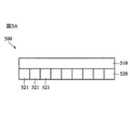
図5Aは、本発明の実施形態に係る、カラーイメージセンサの側面図である。カラーイメージセンサ500は、フィルターアレイ510およびセンサアレイ520を含む。フィルターアレイ510は、赤色フィルター511、緑色フィルター512、および青色フィルター513などの複数のカラーフィルターを含む。例えば、2つの緑色フィルター、1つの赤色フィルター、および1つの青色フィルターは、ベイヤーパターンの2×2のカラーフィルターアレイに配置される。センサアレイ520は、フィルターアレイ510によって入射光を受光する複数の光電素子521を含む。光電素子521は、複数のユニットセル内に配置される。説明の目的のために、図5Aのセンサアレイ520は、センサアレイ520の光電素子の相対的な高さを示していない。
FIG. 5A is a side view of the color image sensor according to the embodiment of the present invention. The
図5Bは、図5Aの実施形態に係る、カラーイメージセンサの上面図である。図5Cは、図5Aの実施形態に係る、カラーイメージセンサの斜視図である。図5Bに示されるように、2×2のアレイに配置されたユニットセル530、540、550、および560は、フィルターアレイ510の2×2のカラーフィルターアレイに対応する2×2のアレイに配置される。従って、ユニットセル530、540、550、および560は、緑色光、青色光、および赤色光を受光し、緑色光は、フィルターアレイ510の2×2のカラーフィルターアレイをそれぞれ通過する。具体的に言うと、マクロユニットセル570の4つのユニットセル530、540、550、および560は、0、π/2、π、および3π/2などの4つの異なる位相の緑色、青色、赤色、および緑色画素を撮像するように構成される。ユニットセル530、540、550、および560の光電素子531〜534、541〜544、551〜554、および561〜564の高さの設計は、センサアレイ520の光電素子が同じ材料でできているとき、上述の式(6)に従うことができる。従って、詳細はここでは省略する。しかしながら、式(6)は、固定波長で単色用に設計されている。
FIG. 5B is a top view of the color image sensor according to the embodiment of FIG. 5A. FIG. 5C is a perspective view of the color image sensor according to the embodiment of FIG. 5A. As shown in FIG. 5B, the
λR、λG、およびλBが赤色光、緑色光、および青色光の波長をそれぞれ表すとした場合、赤色光、緑色光、および青色光の中で赤色光が最長波長を有し、青色光が最短波長を有するため、波長間の関係は、λR>λG>λBであると結論されることができる。よって、センサアレイ520の光電素子が同じ材料でできている場合、赤色光を受光するユニットセル550の光電素子551〜554は、マクロユニットセル570の他のユニットセルの光電素子よりも相対的に大きい高さを有する。即ち、各ユニットセルの光電素子の高さは、受光した光の波長に比例する。
Assuming that λ R , λ G , and λ B represent the wavelengths of red light, green light, and blue light, respectively, red light has the longest wavelength among red light, green light, and blue light; Since light has the shortest wavelength, it can be concluded that the relationship between wavelengths is λ R > λ G > λ B. Therefore, when the photoelectric elements of the
例えば、図5Cに示すように、赤色光を受光するユニットセル550の光電素子551〜554の高さは、同一場所に配置された緑色光を受光するユニットセル530の光電素子531〜534(即ち、同じ位相)の高さよりも相対的に高い。
For example, as shown in FIG. 5C, the height of the
図5Dは、図5Aの実施形態に係る詳細な側面図の部分である。図5Eは、図5Aの実施形態に係る詳細な側面図のもう1つの部分である。図5Dの側面図は、緑色光を受光するユニットセル530の光電素子531〜532と、赤色光を受光するユニットセル550の光電素子551〜552の相対的な高さを示している。同じ位相では、光電素子551は、光電素子531より大きな高さを有し、光電素子552は、光電素子532より大きな高さを有する。
FIG. 5D is a portion of a detailed side view according to the embodiment of FIG. 5A. FIG. 5E is another portion of the detailed side view according to the embodiment of FIG. 5A. The side view of FIG. 5D shows the relative heights of the
図5Eの側面図は、緑色光を受光するユニットセル530の光電素子531〜532と、青色光を受光するユニットセル540の光電素子541〜542の相対的な高さを示している。同じ位相では、光電素子531は、光電素子541より大きな高さを有し、光電素子532は、光電素子542より大きな高さを有する。
The side view of FIG. 5E shows the relative heights of the
マクロユニットセル570は、センサアレイ520に繰り返し配置されるため、4つの位相シフトのホログラム画像は、センサアレイ520のマクロユニットセルの各ユニットセル530、540、550、および560によって撮像された画素を組み合わせることによって得られ、よって、全ての16の位相シフトのホログラム画像を得ることができる。留意すべきことは、ユニットセル530によって撮像された緑色の位相シフトのホログラム画像は、ユニットセル560によって撮像されたホログラム画像と異なることである。例えば、全ての16の位相シフトのホログラム画像は、(Rδ0、Rδ1、Rδ2、Rδ3)、(G1δ0、G1δ1、G1δ2、G1δ3)、(Bδ0、Bδ1、Bδ2、Bδ3)、および(G2δ0、G2δ1、G2δ2、G2δ3)であることができる。緑色の位相シフトのホログラム画像(G2δ0、G2δ1、G2δ2、G2δ3)は、ユニットセル560によって撮像される。
Since the
図6は、本発明の実施形態に係る、カラーイメージセンサに用いる4ステップ位相シフトデジタルホログラフィ法のフローチャートである。図3のフローチャートと異なり、図6のフローチャートは、カラーイメージセンサに用いられるものである。ステップS610では、異なるカラーチャネルおよび異なる位相の16の位相シフトのホログラム画像が得られる。例えば、図5に示されたイメージセンサ500がもちいられることができる。16の位相シフトのホログラム画像は、上述のように、(Rδ0、Rδ1、Rδ2、Rδ3)、(G1δ0、G1δ1、G1δ2、G1δ3)、(Bδ0、Bδ1、Bδ2、Bδ3)、および(G2δ0、G2δ1、G2δ2、G2δ3)である。
FIG. 6 is a flowchart of a four-step phase shift digital holography method used for a color image sensor according to an embodiment of the present invention. Unlike the flowchart of FIG. 3, the flowchart of FIG. 6 is used for a color image sensor. In step S610, hologram images with 16 different phase shifts of different color channels and different phases are obtained. For example, the
ステップS620では、フーリエ領域の各カラーチャネルの物体波は、異なるカラーチャネルおよび異なる位相の16のホログラム画像に基づいて計算される。 In step S620, the object wave of each color channel in the Fourier domain is calculated based on 16 hologram images of different color channels and different phases.
ステップS630では、各カラーチャネルの物体像は、各カラーチャネルの物体波に基づいて再構成される。特に、カラーイメージセンサの1つの赤色チャネル、1つの青色チャネル、および2つの緑色チャネルなどの4つのカラーチャネルがあり、単一のカラーチャネルの物体波の計算および物体像の構成の動作は、図3の実施形態において参照でき、詳細はここでは繰り返されない。 In step S630, the object image of each color channel is reconstructed based on the object wave of each color channel. In particular, there are four color channels, such as one red channel, one blue channel, and two green channels of a color image sensor, and the operation of object wave calculation and object image configuration for a single color channel is illustrated in FIG. 3, and details are not repeated here.
従って、1つの赤色チャネル、1つの青色チャネル、および2つの緑色チャネルを表す4つの物体像は、ステップS330の後に得られ、カラーイメージセンサ500に結合された画像信号処理装置(図示されていない)は、4つの物体像を用いて元のカラーイメージを再構成することができる。
Accordingly, four object images representing one red channel, one blue channel, and two green channels are obtained after step S330 and are image signal processing devices (not shown) coupled to
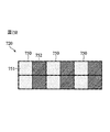
図7Aは、本発明の実施形態に係る、イメージセンサの側面図である。説明の目的のために、例えば、イメージセンサ700は、単色イメージセンサである。図7Aに示されるように、イメージセンサ700は、センサアレイ720を含む。センサアレイ720は、入射光を受光する複数の光電素子721を含む。光電素子721は、半導体製造プロセスによって基板730の上に実装されることができる。留意すべきことは、イメージセンサ700にレンズは用いられず、且つ説明の目的のために、図7Aのセンサアレイ720は、センサアレイの光電素子の相対的な高さ(即ち、厚さ)を示さないことである。
FIG. 7A is a side view of the image sensor according to the embodiment of the present invention. For illustrative purposes, for example,
図7Bは、図7Aの実施形態に係る、イメージセンサの上面図である。
図7Cは、図7Aの実施形態に係るイメージセンサの斜視図である。
FIG. 7B is a top view of the image sensor according to the embodiment of FIG. 7A.
FIG. 7C is a perspective view of the image sensor according to the embodiment of FIG. 7A.
図7Bに示されるように、センサアレイ720は、複数のユニットセル750を含み、各ユニットセルは、2×1アレイに配置された2つの光電素子を有する。例えば、光電素子751と752は、異なる高さであり、各光電素子751と752の高さは、対応するホログラムの特定の位相を表している。例えば、2ステップの直交位相シフトホログラフィ法がセンサアレイ720に用いられ、2つの異なる位相は、0とπ/2であることができる。位相0とπ/2の干渉パターンの強度を得た後、物体光の複素振幅は、以下の式で与えられる。
例えば、光電素子751と752の高さは、以下の式によって計算されることができる:
λは、特定の波長を示し、nは、光電素子の材料の屈折率を示し、且つδmは、与えられた位相値、例えば、0、およびπ/2(またはπおよび3π/2)を示している。留意すべきことは、センサアレイ720の全ての光電素子は、同じ材料で実装されることができるため、同じ屈折率を有することができる。特に、2ステップ位相シフトデジタルホログラフィ法は、イメージセンサ700の構造に用いられる。例えば、光電素子752と752の高さは、位相δ0とδ1にそれぞれ対応するd0とd1である。δ0、およびδ1の値は、それぞれ0とπ/2(またはπおよび3π/2)である。高さd0〜d1が式(10)と整合するため、d0とd1の値は、0とλ/4nとしてそれぞれ計算されることができる。光電素子751と752の高さの違いは、図7Cに示されている。留意すべきことは、ユニットセル750は、センサアレイ720に繰り返し配置され、各ユニットセル750の各光電素子は、2つの異なる位相の個別の位相の画素を撮像することができる。例えば、各ユニットセル750の光電素子751と752は、第1の位相の第1の画素、第2の位相の第2の画素をそれぞれ撮像することができる。第1の画素および第4の画素は、各ユニットセル750の光電素子751と752によって撮像されるため、第1の画素および第2の画素は、実質的に同じである。例えば、δ0のホログラム画像は、各ユニットセル750の光電素子751の撮像された画素から得られることができる。同様に、δ1のホログラム画像は、各ユニットセル750の光電素子752の撮像された画素からそれぞれ得られることができる。
λ indicates a specific wavelength, n indicates the refractive index of the material of the photoelectric device, and δ m indicates a given phase value, for example, 0, and π / 2 (or π and 3π / 2). Is shown. It should be noted that all photoelectric elements of
2つの位相のホログラム画像を得た後、フーリエ領域(domain)の物体波は、式(9)を用いて得ることができる。次いで、逆フーリエ変換が物体波に行われ、空間領域の物体像を再構成する。また、フーリエ領域の物体波を空間領域の物体像に変換する変換関数H(x、y)は、予め推定されることができ、よって、物体波と変換関数との畳み込みが物体像を得るために行われることができる。 After obtaining the two-phase hologram image, the object wave in the Fourier domain can be obtained using equation (9). Next, an inverse Fourier transform is performed on the object wave to reconstruct an object image in the spatial domain. Further, a conversion function H (x, y) for converting an object wave in the Fourier domain into an object image in the spatial domain can be estimated in advance, and convolution of the object wave and the conversion function is to obtain an object image. Can be done.
図7Dは、本発明のもう1つの実施形態に係る、イメージセンサの斜視図である。他の実施形態では、ユニットセル750の光電素子751と752の位置は、図7Bのそれらと同じであるが、図7Dに示されるように、ユニットセル750の光電素子751と752の高さは、同じである。例えば、光電素子751と752は、異なる屈折率を有する異なる材料からできている。具体的に言うと、各光電素子の材料の屈折率は、以下の式に従わなければならない。
式(11)に示すように、高さdは、一定であり、屈折率nmは、可変である。2ステップ位相シフトホログラフィがここで用いられることもできる例えば、2ステップ位相シフトホログラフィ法の位相は、0とπ/2(またはπと3π/2)である。高さdが0.5λと等しいとした場合、光電素子751と752の材料の屈折率は、式(11)を用いて計算されることができる。
As shown in the equation (11), the height d is constant, and the refractive index nm is variable. Two-step phase shift holography can also be used here, for example, the phases of the two-step phase shift holography method are 0 and π / 2 (or π and 3π / 2). Assuming that the height d is equal to 0.5λ, the refractive index of the material of the
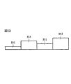
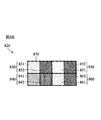
図8Aは、本発明のもう1つの実施形態に係る、カラーイメージセンサの側面図である。カラーイメージセンサ800は、フィルターアレイ810およびセンサアレイ820を含む。フィルターアレイ810は、赤色フィルター、緑色フィルター、および青色フィルターなどの複数のカラーフィルターを含む。例えば、2つの緑色フィルター、1つの赤色フィルター、および1つの青色フィルターは、ベイヤーパターンの2×2のカラーフィルターアレイに配置される。センサアレイ820は、フィルターアレイ810によって光を受光する複数のユニットセル821を含む。説明の目的のために、図8Aのセンサアレイ820は、センサアレイ820の光電素子の相対的な高さを示していない。
FIG. 8A is a side view of a color image sensor according to another embodiment of the present invention. The
図8Bは、図8Aの実施形態に係る、カラーイメージセンサの上面図である。図7Bに示されるように、ユニットセル830、840、850、および860は、緑色光、青色光、赤色光、および緑色光をそれぞれ受光する。各ユニットセル830、840、850、および860は、2つの光電素子を有し、対応するカラーフィルターを有する。例えば、ユニットセル830、840、850、および860は、フィルターアレイ810によって緑色光、青色光、赤色光、および緑色光を受光する。特に、ベイヤーパターンの方式のマクロユニットセル870は、ユニットセル830、840、850、および860を用いて形成されることができる。
FIG. 8B is a top view of the color image sensor according to the embodiment of FIG. 8A. As shown in FIG. 7B,
実施形態では、2ステップ位相シフトホログラフィ法が用いられる。例えば、各ユニットセルの2つの光電素子は、例えば0およびπ/2などの異なる位相の画素を受けるように設計された異なる高さを有する。 In the embodiment, a two-step phase shift holography method is used. For example, the two photoelectric elements of each unit cell have different heights designed to receive pixels of different phases, eg, 0 and π / 2.
ユニットセル830、840、850、および860の光電素子831〜832、841〜842、851〜853、および861〜862の高さの設計は、センサアレイ820の光電素子が同じ材料でできているとき、上述の式(6)に従うことができる。従って、詳細はここでは省略する。しかしながら、式(6)は、固定波長で単色用に設計されている。
The height design of the
λR、λG、およびλBが赤色光、緑色光、および青色光の波長をそれぞれ表すとした場合、赤色光、緑色光、および青色光の中で赤色光が最長波長を有し、青色光が最短波長を有するため、波長間の関係は、λR>λG>λBであると結論されることができる。よって、センサアレイ820の光電素子が同じ材料でできている場合、赤色光を受光するユニットセル850の光電素子851〜852は、マクロユニットセル870の他のユニットセルの光電素子よりも相対的に大きい高さを有する。
Assuming that λ R , λ G , and λ B represent the wavelengths of red light, green light, and blue light, respectively, red light has the longest wavelength among red light, green light, and blue light; Since light has the shortest wavelength, it can be concluded that the relationship between wavelengths is λ R > λ G > λ B. Therefore, when the photoelectric elements of the
図5のセンサアレイ520と比較すると、マクロユニットセルのサイズがセンサアレイ820で4×2であり、マクロユニットセルのサイズがセンサアレイ520で4×4であるため、垂直方向の解像度は、センサアレイ820を用いたとき、2倍である。しかしながら、センサアレイ820を用いて物体波を得る演算量の複雑さは、高くなっている。例えば、2ステップ位相シフトホログラフィ法の物体波は、以下の式を用いて計算されることができる。
このことから、レンズフリーイメージセンサが提供される。4ステップ位相シフトホログラフィのアルゴリズムの異なる位相で設計された、異なる高さを有する光電素子をセンサアレイ内に配置することにより、物体像は、光電素子によって撮像された位相シフトのホログラム画像を用いて再構成されることができる。従って、モジュラー型レンズは、レンズフリーイメージセンサを用いたカメラモジュールに必要でないため、全体的なカメラモジュールのコストを減少することができ、カメラモジュールの厚さは、薄くすることができる。 For this reason, a lens-free image sensor is provided. By arranging photoelectric elements having different heights, designed in different phases of the four-step phase shift holography algorithm, in the sensor array, the object image is formed using a phase-shifted hologram image captured by the photoelectric elements. Can be reconfigured. Therefore, the modular lens is not necessary for the camera module using the lens-free image sensor, so that the cost of the entire camera module can be reduced and the thickness of the camera module can be reduced.
本発明は、例として及び望ましい実施の形態によって記述されているが、本発明は開示された実施形態に限定されるものではない。逆に、当業者には自明の種々の変更及び同様の配置をカバーするものである。よって、添付の特許請求の範囲は、最も広義な解釈が与えられ、全てのこのような変更及び同様の配置を含むべきである。 Although the invention has been described by way of example and by way of preferred embodiments, the invention is not limited to the disclosed embodiments. On the contrary, it is intended to cover various modifications and similar arrangements obvious to one skilled in the art. Accordingly, the appended claims should be accorded the broadest interpretation and should include all such modifications and similar arrangements.
100 位相シフトデジタルホログラフィ装置
101、103 ビームスプリッタ
102 ピエゾ鏡
104 ミラー
110 レーザー光源
111 ビームエミッタ
120 センサアレイ
200 イメージセンサ
220 センサアレイ
221 光電素子
230 基板
250 ユニットセル
251、252、253、254 光電素子
410、420、430、440 ユニットセル
411〜414 光電素子
421〜424 光電素子
431〜434 光電素子
441〜444 光電素子
450 マクロセルユニット
500 カラーイメージセンサ
510 フィルターアレイ
511 赤色フィルター
512 緑色フィルター
513 青色フィルター
520 センサアレイ
521 光電素子
530、540、550、560 ユニットセル
531〜534 光電素子
541〜544 光電素子
551〜554 光電素子
561〜564 光電素子
570 マクロユニットセル
700 イメージセンサ
720 センサアレイ
721 光電素子
730 基板
750 ユニットセル
751 光電素子
752 光電素子
800 カラーイメージセンサ
810 フィルターアレイ
820 センサアレイ
821 ユニットセル
830、840、850、860 ユニットセル
831〜832 光電素子
841〜842 光電素子
851〜853 光電素子
861〜862 光電素子
870 マクロユニットセル
Claims (11)
前記光電素子は、複数のユニットセル内に配置され、各前記ユニットセルは、第1の光電素子および第2の光電素子を含み、
各前記ユニットセルの前記第1の光電素子は、第1の位相の第1の画素を撮像し、各前記ユニットセルの前記第2の光電素子は、第2の位相の第2の画素を撮像し、
前記第1の位相は、前記第2の位相と異なり、
各前記ユニットセルは、第3の位相の第3の画素を撮像する第3の光電素子および第4の位相の第4の画素を撮像する第4の光電素子を更に含み、
前記第1の位相、前記第2の位相、前記第3の位相、および前記第4の位相は異なり、
各前記ユニットセルの前記第1の光電素子、前記第2の光電素子、前記第3の光電素子、および前記第4の光電素子は、特定の材料でできており、且つ異なる高さであり、
前記第1の位相、前記第2の位相、前記第3の位相、および前記第4の位相は、それぞれ0、π/2、π、および3π/2であるイメージセンサ。 Including a plurality of photoelectric elements for receiving incident light,
The photoelectric device is disposed in a plurality of unit cells, each of the unit cells includes a first photoelectric device and a second photoelectric device,
The first photoelectric element of each of the unit cells captures a first pixel of a first phase, and the second photoelectric element of each of the unit cells captures a second pixel of a second phase And
The first phase, Unlike the second phase,
Each of the unit cells further includes a third photoelectric element for imaging a third pixel in a third phase and a fourth photoelectric element for imaging a fourth pixel in a fourth phase;
The first phase, the second phase, the third phase, and the fourth phase are different,
The first photoelectric element, the second photoelectric element, the third photoelectric element, and the fourth photoelectric element of each of the unit cells are made of a specific material and have different heights,
The first phase, the second phase, the third phase, and the fourth phase, respectively 0, [pi / 2, [pi, and 3 [pi] / 2 der Ru image sensor.
物体波は、前記第1の位相シフトのホログラム画像および前記第2の位相シフトのホログラム画像に基づいて計算され、物体像は、逆変換を前記物体波に行うことにより再構成される請求項1に記載のイメージセンサ。 The hologram image of the first phase shift and the hologram image of the second phase shift are obtained by combining the first pixel of the first phase and the second pixel of the second phase captured by the unit cell. It is obtained by combining each,
The object wave is calculated based on the hologram image of the first phase shift and the hologram image of the second phase shift, and the object image is reconstructed by performing an inverse transform on the object wave. An image sensor according to claim 1.
物体波は、前記第1の位相シフトのホログラム画像、前記第2の位相シフトのホログラム画像、前記第3の位相シフトのホログラム画像、および前記第4の位相シフトのホログラム画像に基づいて計算され、物体像は、逆変換を前記物体波に行うことにより再構成される請求項1に記載のイメージセンサ。 The hologram image of the first phase shift, the hologram image of the second phase shift, the hologram image of the third phase shift, and the hologram image of the fourth phase shift are the first phase photographed by the unit cell. By combining the first pixel, the second pixel of the second phase, the third pixel of the third phase, and the fourth pixel of the fourth phase, respectively. ,
The object wave is calculated based on the hologram image of the first phase shift, the hologram image of the second phase shift, the hologram image of the third phase shift, and the hologram image of the fourth phase shift, The image sensor according to claim 1 , wherein an object image is reconstructed by performing an inverse transformation on the object wave.
前記入射光から赤色光を抽出する赤色フィルター、および
前記入射光から青色光を抽出する青色フィルターを含むフィルターアレイを更に含む請求項1に記載のイメージセンサ。 A first green filter and a second green filter that extract green light from incident light;
The image sensor according to claim 1, further comprising: a filter array including a red filter that extracts red light from the incident light, and a blue filter that extracts blue light from the incident light.
各前記マクロユニットセルの前記第1のユニットセル、前記第2のユニットセル、前記第3のユニットセル、および前記第4のユニットセルは、前記第1の緑色フィルター、前記第2の緑色フィルター、前記赤色フィルター、および前記青色フィルターによって、前記緑色光、前記緑色光、前記赤色光、および前記青色光をそれぞれ受光し、
前記第1の緑色フィルター、前記第2の緑色フィルター、前記赤色フィルター、および前記青色フィルターは、ベイヤーパターンに配置され、
各前記マクロユニットセルの前記第1のユニットセル、前記第2のユニットセル、前記第3のユニットセル、および前記第4のユニットセルの前記第1の光電素子と前記第2の光電素子の高さは、前記緑色光、前記緑色光、前記赤色光、および前記青色光の波長にそれぞれ比例する請求項5に記載のイメージセンサ。 The unit cells are arranged in a plurality of macro unit cells, each of the macro unit cells being a first unit cell, a second unit cell, a third unit cell arranged in a 2 × 2 array, and Including a fourth unit cell,
The first unit cell, the second unit cell, the third unit cell, and the fourth unit cell of each of the macro unit cells include the first green filter, the second green filter, The green light, the green light, the red light, and the blue light are received by the red filter and the blue filter, respectively.
The first green filter, the second green filter, the red filter, and the blue filter are arranged in a Bayer pattern,
The height of the first photoelectric element and the second photoelectric element of each of the first unit cell, the second unit cell, the third unit cell, and the fourth unit cell of each of the macro unit cells. The image sensor according to claim 5 , wherein the length is proportional to the wavelengths of the green light, the green light, the red light, and the blue light, respectively.
各前記マクロユニットセルの前記第1のユニットセル、前記第2のユニットセル、前記第3のユニットセル、および前記第4のユニットセルは、前記第1の緑色フィルター、前記第2の緑色フィルター、前記赤色フィルター、および前記青色フィルターによって、前記緑色光、前記緑色光、前記赤色光、および前記青色光をそれぞれ受光し、
各前記ユニットセルは、第3の位相の第3の画素を撮像する第3の光電素子および第4の位相の第4の画素を撮像する第4の光電素子を更に含み、
前記第1の位相、前記第2の位相、前記第3の位相、および前記第4の位相は異なる請求項5に記載のイメージセンサ。 The unit cells are arranged in a plurality of macro unit cells, each of the macro unit cells being a first unit cell, a second unit cell, a third unit cell arranged in a 2 × 2 array, and Including a fourth unit cell,
The first unit cell, the second unit cell, the third unit cell, and the fourth unit cell of each of the macro unit cells include the first green filter, the second green filter, The green light, the green light, the red light, and the blue light are received by the red filter and the blue filter, respectively.
Each of the unit cells further includes a third photoelectric element for imaging a third pixel in a third phase and a fourth photoelectric element for imaging a fourth pixel in a fourth phase;
The image sensor according to claim 5 , wherein the first phase, the second phase, the third phase, and the fourth phase are different.
第5の緑色位相シフトのホログラム画像、第6の緑色位相シフトのホログラム画像、第7の緑色位相シフトのホログラム画像、および第8の緑色位相シフトのホログラム画像は、前記第2のユニットセルによって撮像された前記第1の位相の前記第1の画素、前記第2の位相の前記第2の画素、前記第3の位相の前記第3の画素、および前記第4の位相の前記第4の画素をそれぞれ組み合わせることによって得られ、
第1の赤色位相シフトのホログラム画像、第2の赤色位相シフトのホログラム画像、第3の赤色位相シフトのホログラム画像、および第4の赤色位相シフトのホログラム画像は、前記第3のユニットセルによって撮像された前記第1の位相の前記第1の画素、前記第2の位相の前記第2の画素、前記第3の位相の前記第3の画素、および前記第4の位相の前記第4の画素をそれぞれ組み合わせることによって得られ、
第1の青色位相シフトのホログラム画像、第2の青色位相シフトのホログラム画像、第3の青色位相シフトのホログラム画像、および第4の青色位相シフトのホログラム画像は、前記第4のユニットセルによって撮像された前記第1の位相の前記第1の画素、前記第2の位相の前記第2の画素、前記第3の位相の前記第3の画素、および前記第4の位相の前記第4の画素をそれぞれ組み合わせることによって得られる請求項7に記載のイメージセンサ。 A first green phase shift hologram image, a second green phase shift hologram image, a third green phase shift hologram image, and a fourth green phase shift hologram image are captured by the first unit cell. The first pixel of the first phase, the second pixel of the second phase, the third pixel of the third phase, and the fourth pixel of the fourth phase Are obtained by combining
A fifth green phase shift hologram image, a sixth green phase shift hologram image, a seventh green phase shift hologram image, and an eighth green phase shift hologram image are captured by the second unit cell. The first pixel of the first phase, the second pixel of the second phase, the third pixel of the third phase, and the fourth pixel of the fourth phase Are obtained by combining
A hologram image of a first red phase shift, a hologram image of a second red phase shift, a hologram image of a third red phase shift, and a hologram image of a fourth red phase shift are captured by the third unit cell. The first pixel of the first phase, the second pixel of the second phase, the third pixel of the third phase, and the fourth pixel of the fourth phase Are obtained by combining
The first blue phase shift hologram image, the second blue phase shift hologram image, the third blue phase shift hologram image, and the fourth blue phase shift hologram image are captured by the fourth unit cell. The first pixel of the first phase, the second pixel of the second phase, the third pixel of the third phase, and the fourth pixel of the fourth phase The image sensor according to claim 7 , obtained by combining
第2の緑色の物体波は、前記第6の緑色の位相シフトのホログラム画像、前記第6の緑色の位相シフトのホログラム画像、前記第7の緑色の位相シフトのホログラム画像、および前記第8の緑色の位相シフトのホログラム画像に基づいて計算され、第2の緑色の物体像は、前記逆変換を前記第2の緑色の物体波に行うことにより再構成され、
赤色の物体波は、前記第1の赤色の位相シフトのホログラム画像、前記第2の赤色の位相シフトのホログラム画像、前記第3の赤色の位相シフトのホログラム画像、および前記第4の赤色の位相シフトのホログラム画像に基づいて計算され、赤色の物体像は、前記逆変換を前記赤色の物体波に行うことにより再構成され、
青色の物体波は、前記第1の青色の位相シフトのホログラム画像、前記第2の青色の位相シフトのホログラム画像、前記第3の青色の位相シフトのホログラム画像、および前記第4の青色の位相シフトのホログラム画像に基づいて計算され、青色の物体像は、前記逆変換を前記青色の物体波に行うことにより再構成される請求項8に記載のイメージセンサ。 The first green object wave includes the first green phase shift hologram image, the second green phase shift hologram image, the third green phase shift hologram image, and the fourth green phase shift hologram image. Calculated based on the hologram image of the green phase shift, a first green object image is reconstructed by performing an inverse transformation on the first green object wave;
The second green object wave includes the hologram image of the sixth green phase shift, the hologram image of the sixth green phase shift, the hologram image of the seventh green phase shift, and the eighth hologram image. Calculated based on the hologram image of the green phase shift, a second green object image is reconstructed by performing the inverse transformation on the second green object wave;
The red object wave is a hologram image of the first red phase shift, a hologram image of the second red phase shift, a hologram image of the third red phase shift, and the fourth red phase Calculated based on the hologram image of the shift, the red object image is reconstructed by performing the inverse transformation on the red object wave,
The blue object wave includes the hologram image of the first blue phase shift, the hologram image of the second blue phase shift, the hologram image of the third blue phase shift, and the fourth blue phase shift. 9. The image sensor according to claim 8 , wherein the blue object image is calculated based on the shifted hologram image and reconstructed by performing the inverse transformation on the blue object wave.
前記光電素子は、複数のユニットセル内に配置され、各前記ユニットセルは、第1の光電素子および第2の光電素子を含み、 The photoelectric device is disposed in a plurality of unit cells, each of the unit cells includes a first photoelectric device and a second photoelectric device,
各前記ユニットセルの前記第1の光電素子は、第1の位相の第1の画素を撮像し、各前記ユニットセルの前記第2の光電素子は、第2の位相の第2の画素を撮像し、 The first photoelectric element of each of the unit cells captures a first pixel of a first phase, and the second photoelectric element of each of the unit cells captures a second pixel of a second phase And
前記第1の位相は、前記第2の位相と異なり、 The first phase is different from the second phase,
各前記ユニットセルは、第3の位相の第3の画素を撮像する第3の光電素子および第4の位相の第4の画素を撮像する第4の光電素子を更に含み、 Each of the unit cells further includes a third photoelectric element for imaging a third pixel in a third phase and a fourth photoelectric element for imaging a fourth pixel in a fourth phase;
前記第1の位相、前記第2の位相、前記第3の位相、および前記第4の位相は異なり、 The first phase, the second phase, the third phase, and the fourth phase are different,
各前記ユニットセルの前記第1の光電素子、前記第2の光電素子、前記第3の光電素子、および前記第4の光電素子は、異なる材料でできており、且つ同じ高さであり、 The first photoelectric element, the second photoelectric element, the third photoelectric element, and the fourth photoelectric element of each of the unit cells are made of different materials and have the same height;
前記第1の位相、前記第2の位相、前記第3の位相、および前記第4の位相は、それぞれπ/4、3π/4、5π/8、および7π/8であるイメージセンサ。 The image sensor wherein the first phase, the second phase, the third phase, and the fourth phase are π / 4, 3π / 4, 5π / 8, and 7π / 8, respectively.
Applications Claiming Priority (2)
| Application Number | Priority Date | Filing Date | Title |
|---|---|---|---|
| US15/669,548 US10423122B2 (en) | 2017-08-04 | 2017-08-04 | Lens-free image sensor using phase-shifting hologram |
| US15/669,548 | 2017-08-04 |
Publications (2)
| Publication Number | Publication Date |
|---|---|
| JP2019033467A JP2019033467A (en) | 2019-02-28 |
| JP6677696B2 true JP6677696B2 (en) | 2020-04-08 |
Family
ID=65229527
Family Applications (1)
| Application Number | Title | Priority Date | Filing Date |
|---|---|---|---|
| JP2017214953A Active JP6677696B2 (en) | 2017-08-04 | 2017-11-07 | Lens-free image sensor using phase shift hologram |
Country Status (4)
| Country | Link |
|---|---|
| US (1) | US10423122B2 (en) |
| JP (1) | JP6677696B2 (en) |
| CN (1) | CN109388049B (en) |
| TW (1) | TWI661283B (en) |
Families Citing this family (2)
| Publication number | Priority date | Publication date | Assignee | Title |
|---|---|---|---|---|
| US11317039B1 (en) * | 2021-01-06 | 2022-04-26 | Visera Technologies Company Limited | Image-sensing device |
| TWI811109B (en) * | 2022-09-16 | 2023-08-01 | 國立中正大學 | Hologram detection method |
Family Cites Families (17)
| Publication number | Priority date | Publication date | Assignee | Title |
|---|---|---|---|---|
| JP4188870B2 (en) | 2004-04-06 | 2008-12-03 | 三星電子株式会社 | Hologram medium recording / reproducing apparatus and hologram medium reproducing apparatus |
| JP4455215B2 (en) * | 2004-08-06 | 2010-04-21 | キヤノン株式会社 | Imaging device |
| TWI382753B (en) * | 2007-12-17 | 2013-01-11 | Omnivision Tech Inc | Reflowable camera module with integrated flash |
| JP2010152176A (en) * | 2008-12-25 | 2010-07-08 | Mitsubishi Electric Corp | Projection type display device |
| US9007433B2 (en) | 2009-10-20 | 2015-04-14 | The Regents Of The University Of California | Incoherent lensfree cell holography and microscopy on a chip |
| TWI515885B (en) * | 2009-12-25 | 2016-01-01 | 新力股份有限公司 | Semiconductor device and method of manufacturing the same, and electronic apparatus |
| JP5644177B2 (en) * | 2010-05-07 | 2014-12-24 | ソニー株式会社 | Solid-state imaging device, manufacturing method thereof, and electronic apparatus |
| US10108145B2 (en) | 2012-08-31 | 2018-10-23 | National University Corporation Kyoto Institute Of Technology | Digital holography device and digital holography play method |
| US9549099B2 (en) | 2013-03-12 | 2017-01-17 | Apple Inc. | Hybrid image sensor |
| EP2778601A1 (en) * | 2013-03-15 | 2014-09-17 | Siemens Healthcare Diagnostics Inc. | Optical metrology by light beam analysis |
| US9224881B2 (en) | 2013-04-04 | 2015-12-29 | Omnivision Technologies, Inc. | Layers for increasing performance in image sensors |
| US10061125B2 (en) * | 2014-03-04 | 2018-08-28 | California Institute Of Technology | Directional optical receiver |
| CN104252844B (en) | 2014-09-23 | 2017-04-05 | 京东方科技集团股份有限公司 | Image element circuit and its driving method, organic electroluminescence display panel and display device |
| TWI552594B (en) | 2014-10-27 | 2016-10-01 | 聯詠科技股份有限公司 | Color filter array for image sensing device and manufacturing method thereof |
| JP6686323B2 (en) | 2015-08-13 | 2020-04-22 | 大日本印刷株式会社 | Hologram structure |
| KR102414030B1 (en) | 2015-11-18 | 2022-06-29 | 에스케이하이닉스 주식회사 | Image sensor |
| JP2017110991A (en) * | 2015-12-16 | 2017-06-22 | セイコーエプソン株式会社 | Measurement system, measurement method, robot control method, robot, robot system, and picking device |
-
2017
- 2017-08-04 US US15/669,548 patent/US10423122B2/en active Active
- 2017-11-07 JP JP2017214953A patent/JP6677696B2/en active Active
-
2018
- 2018-05-04 TW TW107115257A patent/TWI661283B/en active
- 2018-06-05 CN CN201810570330.2A patent/CN109388049B/en active Active
Also Published As
| Publication number | Publication date |
|---|---|
| US20190041794A1 (en) | 2019-02-07 |
| JP2019033467A (en) | 2019-02-28 |
| TWI661283B (en) | 2019-06-01 |
| CN109388049B (en) | 2021-01-01 |
| CN109388049A (en) | 2019-02-26 |
| US10423122B2 (en) | 2019-09-24 |
| TW201910941A (en) | 2019-03-16 |
Similar Documents
| Publication | Publication Date | Title |
|---|---|---|
| US11209664B2 (en) | 3D imaging system and method | |
| EP3129813B1 (en) | Low-power image change detector | |
| JP6725526B2 (en) | Imager with image to create spatially encoded image in a distributed manner | |
| JP2018504577A (en) | Epi-illumination Fourier typography imaging for thick film samples | |
| US20110193956A1 (en) | Apparatus and a method for performing a difference measurement of an object image | |
| KR101592380B1 (en) | Non-rigidly coupled, overlapping, non-feedback, optical systems for spatial filtering of fourier transform optical patterns | |
| JPWO2018221025A1 (en) | Imaging device, image processing device, imaging system, image processing method, and recording medium | |
| JP6677696B2 (en) | Lens-free image sensor using phase shift hologram | |
| JP7373015B2 (en) | Imaging method | |
| FR3071342A1 (en) | BAYER MATRIX IMAGE SENSOR | |
| EP2681604B1 (en) | High-resolution imaging system | |
| WO2021003380A1 (en) | Calibration-free phase shifting procedure for self-interference holography | |
| KR102578652B1 (en) | Image-sensing device | |
| KR20180119428A (en) | Apparatus and method for hologram image acquisition | |
| EP3777129B1 (en) | Airborne image sensor taking matrix pictures by temporal shifting and multi-spectral summation | |
| CN114208145A (en) | Image pickup apparatus and method | |
| Jacquot et al. | Digital holography with improved resolution by spatial sampling of holograms | |
| TW202217236A (en) | Three-dimensional measurement device | |
| JP2021184002A (en) | Imaging element for incoherent digital hologram, imaging apparatus, and manufacturing method of the imaging element | |
| FR2860119A1 (en) | Object scenes representation producing device for monitoring surroundings of e.g. aircraft, has filtering unit arranged in intermediate image plane and having two color frames with two different filtering characteristics | |
| De Leon et al. | Spectral characterization of a volume holographic imaging system |
Legal Events
| Date | Code | Title | Description |
|---|---|---|---|
| A621 | Written request for application examination |
Free format text: JAPANESE INTERMEDIATE CODE: A621 Effective date: 20171107 |
|
| A131 | Notification of reasons for refusal |
Free format text: JAPANESE INTERMEDIATE CODE: A131 Effective date: 20190129 |
|
| A02 | Decision of refusal |
Free format text: JAPANESE INTERMEDIATE CODE: A02 Effective date: 20190924 |
|
| A521 | Request for written amendment filed |
Free format text: JAPANESE INTERMEDIATE CODE: A523 Effective date: 20200107 |
|
| A521 | Request for written amendment filed |
Free format text: JAPANESE INTERMEDIATE CODE: A821 Effective date: 20200109 |
|
| A911 | Transfer to examiner for re-examination before appeal (zenchi) |
Free format text: JAPANESE INTERMEDIATE CODE: A911 Effective date: 20200128 |
|
| TRDD | Decision of grant or rejection written | ||
| A01 | Written decision to grant a patent or to grant a registration (utility model) |
Free format text: JAPANESE INTERMEDIATE CODE: A01 Effective date: 20200225 |
|
| A61 | First payment of annual fees (during grant procedure) |
Free format text: JAPANESE INTERMEDIATE CODE: A61 Effective date: 20200313 |
|
| R150 | Certificate of patent or registration of utility model |
Ref document number: 6677696 Country of ref document: JP Free format text: JAPANESE INTERMEDIATE CODE: R150 |
|
| R250 | Receipt of annual fees |
Free format text: JAPANESE INTERMEDIATE CODE: R250 |