JP6671850B2 - Display device and control method thereof - Google Patents
Display device and control method thereof Download PDFInfo
- Publication number
- JP6671850B2 JP6671850B2 JP2015048727A JP2015048727A JP6671850B2 JP 6671850 B2 JP6671850 B2 JP 6671850B2 JP 2015048727 A JP2015048727 A JP 2015048727A JP 2015048727 A JP2015048727 A JP 2015048727A JP 6671850 B2 JP6671850 B2 JP 6671850B2
- Authority
- JP
- Japan
- Prior art keywords
- panel
- control
- transmittance
- light
- display device
- Prior art date
- Legal status (The legal status is an assumption and is not a legal conclusion. Google has not performed a legal analysis and makes no representation as to the accuracy of the status listed.)
- Expired - Fee Related
Links
- 238000000034 method Methods 0.000 title claims description 41
- 238000009826 distribution Methods 0.000 claims description 101
- 238000009499 grossing Methods 0.000 claims description 56
- 238000002834 transmittance Methods 0.000 claims description 52
- 238000005259 measurement Methods 0.000 claims description 5
- 230000001678 irradiating effect Effects 0.000 claims description 4
- 239000004973 liquid crystal related substance Substances 0.000 description 100
- 238000004364 calculation method Methods 0.000 description 32
- 238000010586 diagram Methods 0.000 description 12
- 230000006870 function Effects 0.000 description 6
- 230000000694 effects Effects 0.000 description 5
- 239000002131 composite material Substances 0.000 description 3
- 230000009977 dual effect Effects 0.000 description 3
- 230000005540 biological transmission Effects 0.000 description 2
- 230000007812 deficiency Effects 0.000 description 2
- 230000015572 biosynthetic process Effects 0.000 description 1
- 230000001771 impaired effect Effects 0.000 description 1
- 238000003786 synthesis reaction Methods 0.000 description 1
Images


Landscapes
- Liquid Crystal (AREA)
- Liquid Crystal Display Device Control (AREA)
- Control Of Indicators Other Than Cathode Ray Tubes (AREA)
Description
本発明は、表示装置及びその制御方法に関するものである。 The present invention relates to a display device and a control method thereof.
従来、液晶が1枚で構成された透過型の液晶表示装置では、バックライト光が漏れることで、コントラストが低減してしまう課題があった。
コントラストの向上を図る1つの方法として、従来の液晶(以降、1次液晶と称する)とバックライトの間にさらに液晶(以降、2次液晶と称する)を挟んだ2重構成にする技術があった。これにより、2枚の表示階調数の積に等しい階調数を表現できるため、コントラストを改善することが可能となった(特許文献1)。
コントラストの向上を図る別の方法として、画面を複数のバックライト制御エリアに分割し、画像データの特徴量に基づいてバックライトの輝度と液晶の透過率を制御する技術があった。これにより、エリア毎にバックライト光を制御することで黒浮きを抑制し、コントラストを改善することが可能となった(特許文献2)。
液晶の透過率を制御する理由を以下に説明する。バックライトの点灯状態をエリア毎に制御すると、バックライトの輝度分布が発生する。画像の輝度を忠実に再現することが求められる表示装置においては、出力輝度がバックライトの輝度分布の影響をうけるため、バックライトの輝度分布は画像の輝度再現性に影響する。このため、輝度分布を平滑化処理する必要があった。特許文献2では、これに鑑みて輝度分布の平滑化処理を液晶の透過率に加味して制御していた。
Conventionally, in a transmissive liquid crystal display device including a single liquid crystal, there is a problem in that contrast is reduced due to leakage of backlight light.
As one method of improving the contrast, there is a technique of forming a double structure in which a liquid crystal (hereinafter, referred to as a secondary liquid crystal) is further interposed between a conventional liquid crystal (hereinafter, referred to as a primary liquid crystal) and a backlight. Was. As a result, the number of gradations equal to the product of the two display gradation numbers can be expressed, so that the contrast can be improved (Patent Document 1).
As another method of improving the contrast, there is a technique of dividing a screen into a plurality of backlight control areas and controlling the luminance of the backlight and the transmittance of the liquid crystal based on the feature amount of the image data. Thus, by controlling the backlight light for each area, it is possible to suppress the floating of black and improve the contrast (Patent Document 2).
The reason for controlling the transmittance of the liquid crystal will be described below. When the lighting state of the backlight is controlled for each area, a luminance distribution of the backlight occurs. In a display device that is required to faithfully reproduce the luminance of an image, the output luminance is affected by the luminance distribution of the backlight, and the luminance distribution of the backlight affects the luminance reproducibility of the image. For this reason, it was necessary to smooth the luminance distribution. In Patent Document 2, in view of this, the brightness distribution smoothing process is controlled in consideration of the transmittance of the liquid crystal.
さらに、前述したバックライトの輝度分布だけではなく、液晶パネルにムラがあると、出力輝度の均一性が損なわれるために表示品位が低下する課題があった。液晶パネルのムラは、一般に液晶分子の厚さなどが原因で発生することが多く、液晶パネル毎にムラの特性が異なっていた。1枚の液晶パネルとバックライトで構成された表示装置における、液晶パネルのムラ補正処理の一つとして、出力輝度が最も暗い画素に合わせて補正処理をする方法があった。しかしながら、液晶パネルが複数枚重ね合わされた構造の表示装置では、液晶パネル毎に独立でムラ補正処理をすると、液晶パネル透過後の出力輝度は、重ね合わせた液晶パネルの毎数分輝度低下する。画像の輝度を忠実に再現することが求められる表示装置においては、輝度低下分をバックライト制御値の上昇で補正する必要があった。そこで、複数の液晶パネルを重ねた表示装置において、出力輝度の均一性を維持する1つの方法として、最表面以外に白黒パネルを配置し、白黒パネルに対して輝度ムラを補正する技術があった(特許文献3)。 Furthermore, when there is unevenness in the liquid crystal panel as well as in the above-described backlight luminance distribution, there is a problem that the display quality deteriorates because the uniformity of the output luminance is impaired. In general, the unevenness of a liquid crystal panel often occurs due to the thickness of liquid crystal molecules and the like, and the characteristics of the unevenness differ from one liquid crystal panel to another. As one of the unevenness correction processes of a liquid crystal panel in a display device including one liquid crystal panel and a backlight, there is a method of performing a correction process in accordance with a pixel having the lowest output luminance. However, in a display device having a structure in which a plurality of liquid crystal panels are superimposed, if unevenness correction processing is performed independently for each liquid crystal panel, the output luminance after passing through the liquid crystal panels is reduced by the number of the superposed liquid crystal panels. In a display device that is required to faithfully reproduce the luminance of an image, it is necessary to correct a decrease in luminance by increasing a backlight control value. Therefore, in a display device in which a plurality of liquid crystal panels are superimposed, as one method for maintaining the uniformity of the output luminance, there is a technique of disposing a black and white panel other than the outermost surface and correcting luminance unevenness with respect to the black and white panel. (Patent Document 3).
しかしながら、特許文献3ではバックライトが全エリア点灯している状態での技術であるため、バックライトのエリア制御による高コントラスト化ができなかった。本発明は、上記の事情に鑑みてなされたもので、液晶パネルの2重構造とバックライトのエリア制御で構成された表示装置において、液晶パネルのムラの改善と、バックライトのエリア制御による高コントラスト化を両立させる技術を提供することを目的とする。 However, in Patent Literature 3, since the backlight is lit in all areas, high contrast cannot be achieved by controlling the area of the backlight. The present invention has been made in view of the above circumstances, and in a display device having a dual structure of a liquid crystal panel and area control of a backlight, it is possible to improve unevenness of the liquid crystal panel and to achieve high performance by controlling the area of the backlight. It is an object of the present invention to provide a technique for achieving both contrast enhancement.
本発明は、
光の透過率を制御可能な第1パネルと、
前記第1パネルの背面側に設けられ、光の透過率を制御可能な第2パネルと、
前記第2パネルの背面側に設けられ、独立に輝度を制御可能な複数の制御エリアからなる発光手段と、
各制御エリアに対応する画像データの各分割エリアにおける特徴量に基づき前記各制御エリアの制御値を設定する設定手段と、
前記画像データに基づき前記第1パネルの透過率を制御する第1制御手段と、
前記各制御エリアの制御値に基づき、前記第2パネルの透過率を制御する第2制御手段と、
を備え、
前記発光手段は設定された制御値に基づいて前記各制御エリアの発光を制御し、
前記第2制御手段は、前記各制御エリアについて、前記発光手段から前記第2パネルに照射される照射光の輝度分布を前記各制御エリアの制御値に基づき算出し、前記照射光が前記第2パネルを透過することによって前記第1パネルに照射される光の輝度分布を平滑化するための第1平滑化ゲインを前記照射光の輝度分布に基づき算出し、前記第1平滑化ゲインに基づき前記第2パネルの透過率を制御する
ことを特徴とする表示装置
である。
The present invention
A first panel capable of controlling light transmittance;
A second panel provided on the back side of the first panel and capable of controlling light transmittance;
A light-emitting means provided on the back side of the second panel and comprising a plurality of control areas capable of independently controlling luminance;
Setting means for setting a control value of each control area based on a feature amount in each divided area of image data corresponding to each control area,
First control means for controlling the transmittance of the first panel based on the image data;
Second control means for controlling the transmittance of the second panel based on the control value of each control area;
With
The light emitting means controls light emission of each of the control areas based on a set control value,
The second control means, for each control area, the brightness distribution from the light emitting means irradiating light irradiated to the second panel based-out out calculated the the control value of the control area, the irradiation light is the A first smoothing gain for smoothing a luminance distribution of light irradiated on the first panel by transmitting the light through the second panel is calculated based on the luminance distribution of the irradiated light, and the first smoothing gain is calculated as the first smoothing gain. A display device, wherein the transmittance of the second panel is controlled based on the control signal.
本発明は、
光の透過率を制御可能な第1パネルと、
前記第1パネルの背面側に設けられ、光の透過率を制御可能な第2パネルと、
前記第2パネルの背面側に設けられ、独立に輝度を制御可能な複数の制御エリアからなる発光手段と、
を備えた表示装置の制御方法であって、
各制御エリアに対応する画像データの各分割エリアにおける特徴量に基づき前記各制御エリアの制御値を設定する設定工程と、
前記画像データに基づき前記第1パネルの透過率を制御する第1制御工程と、
前記各制御エリアの制御値に基づき、前記第2パネルの透過率を制御する第2制御工程と、
を有し、
前記発光手段は設定された制御値に基づいて前記各制御エリアの発光を制御し、
前記第2制御工程で、前記各制御エリアについて、前記発光手段から前記第2パネルに照射される照射光の輝度分布を前記各制御エリアの制御値に基づき算出し、前記照射光が前記第2パネルを透過することによって前記第1パネルに照射される光の輝度分布を平滑化するための第1平滑化ゲインを前記照射光の輝度分布に基づき算出し、前記第1平滑化ゲインに基づき前記第2パネルの透過率を制御する
ことを特徴とする表示装置の制御方法
である。
The present invention
A first panel capable of controlling light transmittance;
A second panel provided on the back side of the first panel and capable of controlling light transmittance;
A light-emitting means provided on the back side of the second panel and comprising a plurality of control areas capable of independently controlling luminance;
A control method of a display device comprising:
A setting step of setting a control value of each control area based on a feature amount in each divided area of image data corresponding to each control area,
A first control step of controlling the transmittance of the first panel based on the image data;
A second control step of controlling a transmittance of the second panel based on a control value of each control area;
Has,
The light emitting means controls light emission of each of the control areas based on a set control value,
In the second control step, said each control area, the brightness distribution from the light emitting means irradiating light irradiated to the second panel based-out out calculated the the control value of the control area, the irradiation light is the A first smoothing gain for smoothing a luminance distribution of light irradiated on the first panel by transmitting the light through the second panel is calculated based on the luminance distribution of the irradiated light, and the first smoothing gain is calculated as the first smoothing gain. And controlling the transmittance of the second panel based on the control signal.
本発明によれば、液晶パネルの2重構造とバックライトのエリア制御で構成された表示装置において、液晶パネルのムラの改善と、バックライトのエリア制御による高コントラスト化を両立できる。 ADVANTAGE OF THE INVENTION According to this invention, in the display apparatus comprised by the dual structure of the liquid crystal panel and the area control of a backlight, the improvement of the unevenness of a liquid crystal panel and the high contrast by the area control of a backlight can be compatible.
(実施例1)
実施例1における表示装置の機能を示したブロック図を図1に示し、表示装置の構成を図2に示す。
図1の表示装置1は、特徴量取得部101、制御値算出部102、輝度分布算出部103、平滑化処理部104、合成ムラ補正ゲイン保存部105、2次液晶開口率決定部106、バックライト部107、2次液晶部108、1次液晶部109から構成される。
(Example 1)
FIG. 1 is a block diagram illustrating the functions of the display device according to the first embodiment, and FIG. 2 illustrates the configuration of the display device.
The display device 1 in FIG. 1 includes a feature
図1の構成で、特徴量取得部101は、入力画像データを取得して複数の分割エリアに分割し、各分割エリア内の画像の特徴量を取得する。実施例1では、特徴量取得部101は、特徴量として分割エリア内の画像の画素値の最大値(以降、最大画素値)を取得する。最大画素値は制御値算出部102へ送信される。
制御値算出部102は、特徴量取得部101から各分割エリアの特徴量(ここでは最大画素値)を取得し、特徴量に基づき各分割エリアに対応する制御エリアのバックライト制御値を算出する。制御値算出部102は、算出したバックライト制御値を輝度分布算出部103とバックライト部107へ送信する。
In the configuration of FIG. 1, the feature
The control
輝度分布算出部103は、制御値算出部102から制御エリア毎のバックライト制御値を取得し、バックライト全体の輝度分布を算出する。輝度分布算出部103は、算出した輝度分布の情報を平滑化処理部104へ送信する。
平滑化処理部104は、輝度分布算出部103から輝度分布情報を取得し、輝度分布情報に基づき、輝度分布を相殺して平滑化するための平滑化ゲイン(第1平滑化ゲイン)を算出する。算出した平滑化ゲイン情報は2次液晶開口率決定部106へ送信される。
The luminance
The smoothing
合成ムラ補正ゲイン保存部105は、1次液晶と2次液晶のムラ補正ゲインを合成した合成ムラ補正ゲインを保持し、2次液晶開口率決定部106へ送信する。合成ムラ補正ゲインは、2次液晶(第2パネル)へ入射した光が2次液晶及び1次液晶(第1パネル)を透過して1次液晶から出射する際の光の透過率の画素毎のばらつきの情報(ムラ情報)である。実施例1では、合成ムラ補正ゲインは、予め測定により求められ、合成ムラ補正ゲイン保存部105に格納されているものとする。また、合成ムラ補正ゲイン保存部105は、合成ムラ補正ゲインの測定時に、2次液晶の透過光の輝度分布の最小値が基準の輝度より小さい場合に、バックライト制御値を増加補正するために用いられる調整ゲインの情報をも記憶している。調整ゲインの情報は、制御値算出部102に出力され、制御値算出部102は、画像の特徴量に基づき算出した調整ゲインに調整ゲインを乗じて最終的なバックライト制御値とする。合成ムラ補正ゲイン及び調整ゲインについての詳細は後述する。
The combined unevenness correction
2次液晶開口率決定部106は、平滑化処理部104の平滑化ゲイン情報と合成ムラ補正ゲイン保存部105の合成ムラ補正ゲインを取得し、2次液晶部108の開口率(透過率)を決定する。2次液晶開口率情報は、2次液晶部108へ送信される。
バックライト部107は、2次液晶部108の背面側に設けられ、独立に輝度を制御可能な複数の制御エリアからなる発光手段である。バックライト部107は、制御値算出部102にて制御エリア毎に算出されたバックライト制御値を取得し、バックライト制御値で各制御エリアの光源を点灯させる。
The secondary liquid crystal aperture
The
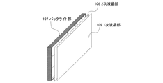
2次液晶部108は、1次液晶部109の背面側に設けられ、光の透過率を制御可能な第2パネル(2次液晶)である。2次液晶部108は、2次液晶開口率決定部106で決定された画素毎の開口率に基づき画素毎に開口率(透過率)が制御される。
1次液晶部109は、光の透過率を制御可能な第1パネル(1次液晶)と、画像データに基づき第1パネルの透過率を制御する第1制御手段と、を含む機能ブロックである。1次液晶部109は、入力画像データに基づき、画素毎に開口率(透過率)が制御される。
実施例1における表示装置の構成は、図2に示すように1次液晶部109を表示面とし
、1次液晶部109の背面に2次液晶部108が配置され、2次液晶部108の背面にバックライト部107が配置される。
The secondary
The primary
In the configuration of the display device according to the first embodiment, as shown in FIG. 2, the primary
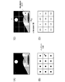
以下に実施例1における表示装置の処理内容について、図3(A)に示すモノクロの8ビット入力画像データを例に説明する。実施例1では、同ピクセルサイズのモノクロ液晶2枚と白色バックライトで構成されているものとする。さらに、入力画像データの画素値が255のときに、出力画像の輝度が基準輝度となるように制御される。基準輝度はここでは200cd/m2とする。基準輝度のことを、出力設定輝度値と称し、LSetで表す。ガンマは1.0であるものとする。さらに、1次液晶と2次液晶のコントラスト比は、いずれも100:1で構成されているものとする。 Hereinafter, the processing contents of the display device according to the first embodiment will be described using the monochrome 8-bit input image data illustrated in FIG. 3A as an example. In the first embodiment, it is assumed that the backlight unit includes two monochrome liquid crystals having the same pixel size and a white backlight. Further, when the pixel value of the input image data is 255, control is performed so that the luminance of the output image becomes the reference luminance. Here, the reference luminance is 200 cd / m 2 . The reference luminance is referred to as an output setting luminance value and is represented by LSet. Gamma is assumed to be 1.0. Further, the contrast ratio between the primary liquid crystal and the secondary liquid crystal is assumed to be 100: 1.
実施例1では、図3(B)に示すようにバックライトの制御エリアが縦方向に3、横方向に4のエリアに分割されており、特徴量取得エリアも同様のエリアに分割されているものとする。このときの入力画像データと特徴量取得エリアの関係を図3(C)に示し、以降の説明においては、入力画像データを図3(C)中の線分ABで切断した一次元データをもとに説明する。図3(C)中の線分AB間で切断したときの一次元の画素値分布を図4に示し、特徴量取得部101でのエリア毎の出力結果を図3(D)に示す。
In the first embodiment, as shown in FIG. 3B, the control area of the backlight is divided into 3 areas in the vertical direction and 4 areas in the horizontal direction, and the feature amount acquisition area is also divided into similar areas. Shall be. FIG. 3C shows the relationship between the input image data and the feature amount acquisition area at this time. In the following description, one-dimensional data obtained by cutting the input image data along the line segment AB in FIG. This will be explained. FIG. 4 shows a one-dimensional pixel value distribution when cutting is performed between the line segments AB in FIG. 3C, and FIG. 3D shows an output result for each area by the feature
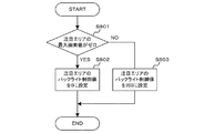
実施例1におけるバックライト制御値算出方法について一例を示す。実施例1では、エリア毎に最大画素値がゼロか否かによって、バックライト制御値を2種類に決定する。バックライト制御値と出力設定輝度値とは相関関係があるため、実施例1では便宜上、バックライト制御値を0又は200の2段階で設定する。以下に、バックライト制御値算出方法の手順を図5に示すフロー図を用いて説明する。ステップS801にて、注目エリアの最大画素値がゼロか否かを判定する。最大画素値がゼロの場合には、ステップS802にてバックライト制御値をゼロに設定し、ゼロでない場合には、ステップS803にて、200に設定する。以上のステップを経るとエリア毎のバックライト制御値が図6(A)として得られる。 An example of a method of calculating a backlight control value according to the first embodiment will be described. In the first embodiment, two types of backlight control values are determined depending on whether or not the maximum pixel value is zero for each area. Since the backlight control value and the output setting luminance value have a correlation, in the first embodiment, the backlight control value is set in two stages of 0 or 200 for convenience. Hereinafter, the procedure of the backlight control value calculation method will be described with reference to the flowchart shown in FIG. In step S801, it is determined whether the maximum pixel value of the attention area is zero. If the maximum pixel value is zero, the backlight control value is set to zero in step S802; otherwise, it is set to 200 in step S803. After the above steps, the backlight control value for each area is obtained as FIG.
実施例1におけるバックライト輝度分布の算出方法について一例を示す。実施例1では、図3(B)に示すようにバックライト光源はエリアの中心に位置し、バックライト制御値によって発光するエリア毎のバックライト輝度分布は、ガウス分布に従うものとする。さらに、画面全体でのバックライト輝度分布は光の重ね合わせの原理に従い、エリア毎のバックライト輝度分布を足す(重ね合わせる)ことで表現できるものとする。このとき、線分ABで発生するエリア毎のバックライト輝度分布と全エリアでのバックライト輝度分布は、それぞれ図6(B)の1001と1002に示す分布を持つ。エリア内のバックライト輝度分布が平滑になればバックライトの輝度分布に依存しなくなるため、エリア内での輝度再現性を維持できる。エリア内での輝度再現性を維持できる輝度分布(以降、バックライト平滑化輝度分布と称する)は図6(B)の1003に示す輝度分布となる。バックライト平滑化輝度分布は、図6(A)に示すバックライト制御値に基づき決まる。なお、エリア毎のバックライトのピーク輝度が出力設定輝度値超過を許容している理由の一つは、全エリアのバックライト輝度分布を算出した際に、エリアの縁で輝度が不足するのを防ぐためである。もう一つの理由は後述する合成ムラ補正後の出力輝度低減に伴う輝度値低下を防ぐためである。 An example of a method for calculating a backlight luminance distribution in the first embodiment will be described. In the first embodiment, as shown in FIG. 3B, the backlight light source is located at the center of the area, and the backlight luminance distribution for each area that emits light according to the backlight control value follows a Gaussian distribution. Further, the backlight luminance distribution over the entire screen can be expressed by adding (overlapping) the backlight luminance distribution for each area in accordance with the principle of light superposition. At this time, the backlight luminance distribution for each area generated by the line segment AB and the backlight luminance distribution for all areas have distributions indicated by 1001 and 1002 in FIG. 6B, respectively. If the backlight luminance distribution in the area becomes smooth, it will not depend on the luminance distribution of the backlight, so that the luminance reproducibility in the area can be maintained. A luminance distribution that can maintain luminance reproducibility in the area (hereinafter, referred to as a backlight smoothed luminance distribution) is a luminance distribution indicated by 1003 in FIG. The backlight smoothed luminance distribution is determined based on the backlight control values shown in FIG. One of the reasons that the peak luminance of the backlight for each area allows the output setting luminance value to be exceeded is that when the backlight luminance distribution of all areas is calculated, the lack of luminance at the edge of the area is considered. This is to prevent it. Another reason is to prevent a decrease in luminance value due to a decrease in output luminance after the correction of combining unevenness described later.
実施例1におけるバックライト輝度分布平滑化処理について、はじめに目的を述べる。バックライト輝度分布平滑化処理では、図6(B)の1002に示した全エリアのバックライト輝度分布を図6(B)の1003に示すバックライト平滑化輝度分布にするためのゲインを算出することが目的である。以降、前述したゲインをバックライト輝度平滑化ゲインと称する。 First, the purpose of the backlight luminance distribution smoothing process in the first embodiment will be described. In the backlight luminance distribution smoothing processing, a gain is calculated for converting the backlight luminance distribution of all areas shown by 1002 in FIG. 6B into the backlight smoothed luminance distribution shown by 1003 in FIG. That is the purpose. Hereinafter, the above-mentioned gain is referred to as a backlight luminance smoothing gain.
次いで、バックライト輝度平滑化ゲインを算出するまでの処理手順を、図7に示すフロー図を用いて詳細を説明する。なお、算出方法で数式を扱うため、ここでは、2次液晶の画素位置をYとして定義する。
ステップS1101にて、平滑化処理部104は、輝度分布算出部103から算出した全エリアのバックライト輝度分布をLReal(Y)として取得する。取得した全エリアのバックライト輝度分布は前述したように、エリア毎のバックライト輝度分布を足し合わせて図6(B)の1002となる。
次に、ステップS1102にて、平滑化処理部104は、バックライト平滑化輝度分布をLFlat(Y)として取得する。ここで、前述したように、バックライト制御値と出力設定輝度値には相関があるため、バックライト平滑化輝度分布は全エリアにわたり、200cd/m2で設定されて図6(B)の1003となる。
Next, a processing procedure until a backlight luminance smoothing gain is calculated will be described in detail with reference to a flowchart shown in FIG. In addition, since a mathematical expression is used in the calculation method, the pixel position of the secondary liquid crystal is defined as Y here.
In step S1101, the smoothing
Next, in step S1102, the smoothing
最後に、ステップS1103にて、平滑化処理部104は、全エリアのバックライト輝度分布とバックライト平滑化輝度分布からバックライト輝度平滑化ゲインを算出する。バックライト輝度平滑化ゲインをBlGain(Y)とすると、バックライト輝度平滑化ゲインは式101で算出することができる。
BlGain(Y)=LFlat(Y)/LReal(Y)・・・・式101
式101で算出されたゲインの分布を図6(C)の1201に示す。
以上の処理手順を踏まえると、バックライト平滑化輝度分布は、図6(B)の1003となる。
Finally, in step S1103, the smoothing
BlGain (Y) = LFFlat (Y) / LReal (Y)
The distribution of the gain calculated by
Based on the above processing procedure, the backlight smoothed luminance distribution becomes 1003 in FIG.
実施例1における合成ムラ補正ゲイン保存部105が保持する合成ムラ補正ゲインの算出方法について処理手順を図8に示すフロー図を用いて詳細を説明する。ここで説明する合成ムラ補正ゲインの算出は、表示装置1の組み立て時や工場出荷時等に実施され、算出結果が合成ムラ補正ゲイン保存部105に保存された上で、表示装置1が出荷される。ただし、表示装置1が合成ムラ補正ゲインを取得する方法はこれに限らない。使用過程にある表示装置1に対し、外部から合成ムラ補正ゲインの情報を供給することによって表示装置1が合成ムラ補正ゲインを取得する構成でも良い。この場合、例えばUSBメモリやCD−ROM等の可搬記憶媒体を表示装置1に接続して当該可搬記憶媒体に記憶された合成ムラ補正ゲインの情報を読み出すことができる。また、合成ムラ補正ゲインの情報を記憶した外部装置と表示装置1とをUSBケーブルやLANケーブル等の有線や赤外線やBluetooth(登録商標)、無線LAN等の無線で接続し、当該外部装置から合成ムラ補正ゲインを取得することもできる。
The processing procedure of the method of calculating the combined unevenness correction gain held by the combined unevenness correction
図9にムラ補正ゲインを算出するための構成例を示す。図9に示すように表示装置1401と2次元輝度分布測定器1402とムラ補正ゲイン算出装置1403で構成される。なお、ここでは、2次元輝度分布測定器1402とムラ補正ゲイン算出装置1403は表示装置1401に対し外部装置として説明するが、ムラ補正ゲイン算出装置1403の機能を表示装置1401が有する構成でも良い。その場合、図1の表示装置1の構成において、ムラ補正ゲイン算出装置1403の機能を有するブロックがさらに備わる構成となる。当該ムラ補正ゲイン算出装置1403に相当する機能ブロックから出力される合成ムラ補正ゲインの情報は、合成ムラ補正ゲイン保存部105に格納され、保持される。ムラ補正ゲイン算出装置1403の機能を表示装置が有する構成では、使用過程にある表示装置において、1次液晶や2次液晶のムラに経年変化が生じた場合でも、最新のムラの状態を反映させた合成ムラ補正ゲインを用いて表示制御をすることが可能になる。そのため、長期間にわたってムラの少ない表示を行うことが可能になる。
FIG. 9 shows a configuration example for calculating the unevenness correction gain. As shown in FIG. 9, a display device 1401, a two-dimensional luminance distribution measuring device 1402, and an unevenness correction
図8のフローチャートにおいて、初めに、ステップS1301にて、ムラ補正ゲイン算
出装置1403は、表示装置1401から出力される輝度分布(以降、出力輝度分布と称する)を取得する。2次元輝度分布測定器1402は、出力輝度分布を2次元で取得する。
In the flowchart of FIG. 8, first, in step S1301, the unevenness correction
ここで、出力輝度分布取得時の入力画像データと、2次液晶の開口率設定について詳細を説明する。精度の高いムラ補正ゲインを生成するためには、輝度のバラつきの振り幅を最大にする必要があるため、出力輝度分布取得時には輝度値が最大となる所定の画像データ(ここでは、全画面白の画像データ)を入力する。一方、2次液晶の開口率としてはバックライト輝度平滑化ゲインを設定する必要がある。これは、バックライトの輝度分布が平滑化されないと、バックライトの輝度分布が合成ムラ補正ゲインに重畳されてしまい、精度の高いムラ補正ゲインを生成できないからである。上記手順により取得した出力輝度分布は1次液晶と2次液晶の合成ムラのみが重畳されて出力されるため、この輝度分布のバラつきが合成ムラと等しくなる。上記手順によって取得した表示装置の出力輝度分布のうち、図3(C)中の線分AB間における出力輝度分布を図10(A)の1501に示し、LOut(Y)とする。 Here, the input image data at the time of obtaining the output luminance distribution and the setting of the aperture ratio of the secondary liquid crystal will be described in detail. In order to generate a highly accurate unevenness correction gain, it is necessary to maximize the variation width of the luminance variation. Therefore, when acquiring the output luminance distribution, predetermined image data (in this case, full-screen white Image data). On the other hand, it is necessary to set a backlight luminance smoothing gain as the aperture ratio of the secondary liquid crystal. This is because if the luminance distribution of the backlight is not smoothed, the luminance distribution of the backlight is superimposed on the combined unevenness correction gain, and a highly accurate unevenness correction gain cannot be generated. Since the output luminance distribution obtained by the above procedure is output with only the combined unevenness of the primary liquid crystal and the secondary liquid crystal superimposed, the variation in the brightness distribution is equal to the combined unevenness. Among the output luminance distributions of the display device obtained by the above procedure, the output luminance distribution between the line segments AB in FIG. 3C is shown as 1501 in FIG.
次いで、ステップS1302にて、ムラ補正ゲイン算出装置1403は、表示装置の出力輝度分布の中での最小輝度値を取得する。最小輝度値をLOutMinとすると、図10(A)よりLOutMin=200cd/m2となる。
次いで、ステップS1303にて、ムラ補正ゲイン算出装置1403は、出力輝度分布と最小輝度値から合成ムラ補正ゲインを算出する。合成ムラ補正ゲインをMrGain(Y)とすると、合成ムラ補正ゲインは式102で算出することができる。
MrGain(Y)= LOutMin/LOut(Y)・・・・式102
式102で算出された実施例1における合成ムラ補正ゲインの分布を図10(B)の1601に示す。
次いで、ステップS1304にて、ムラ補正ゲイン算出装置1403は、出力輝度分布の最小輝度値と出力設定輝度値を比較し、値が一致するときは処理を終了し、一致しなければ、ステップ1305へ進む。図10(A)の例では、最小輝度値は200であり、出力設定輝度値と一致しているので、ステップS1304で処理終了となる。ここでは、ムラ補正ゲイン算出装置1403が合成ムラ補正ゲインMrGain(Y)を算出して合成ムラ補正ゲイン保存部105に格納する例を説明した。しかし、出力輝度分布LOut(Y)と最小輝度値LOutMinの情報を合成ムラ補正ゲイン保存部105に格納しても良い。この場合、表示装置1において、式102に基づく合成ムラ補正ゲインMrGain(Y)の算出を行うようにすればよい。
Next, in step S1302, the unevenness correction
Next, in step S1303, the unevenness correction
MrGain (Y) = LOutMin / LOut (Y)
The distribution of the combined unevenness correction gain in Example 1 calculated by
Next, in step S1304, the unevenness correction
一方、最小輝度値と出力設定輝度値とが一致していない場合、前述のステップS803で決定したバックライト制御値でバックライト部107を制御すると、輝度に過不足が発生し、輝度再現性が維持されない。そこで、この場合、ムラ補正ゲイン算出装置1403は、ステップ1305において、最小輝度値を出力設定調整ゲインと一致させるための調整ゲインを算出する。以下に処理の詳細を説明する。ムラ補正ゲイン算出装置1403は、出力輝度分布の最小値であるLOutMinと出力設定輝度値であるLSetからバックライト制御値の過不足を低減するための調整ゲインを算出する。このときの調整ゲインをAdGainとすると、式103で算出することができる。
AdGain = LSet/LOutMin・・・・式103
算出された調整ゲインAdGainは、合成ムラ補正ゲインとともに、合成ムラ補正ゲイン保存部105に保存される。調整ゲインAdGainは、制御値算出部102に出力
される。制御値算出部102は、合成ムラ補正ゲイン保存部105から調整ゲインAdGainが入力される場合には、調整ゲインAdGainを前述のステップS803で設定した200に乗算して、最終的なバックライト制御値とする。こうすることにより、バックライト輝度の過不足を低減することができ、輝度再現性を維持することができる。
On the other hand, when the minimum luminance value does not match the output setting luminance value, when the
AdGain = LSet /
The calculated adjustment gain AdGain is stored in the combined unevenness correction
実施例1における2次液晶開口率決定方法について詳細を説明する。2次液晶開口率決定部106は、2次液晶開口率を、合成ムラ補正ゲインとバックライト輝度平滑化ゲインを乗算することで決定する。実施例1における2次液晶開口率の分布を図11(A)の1701に示す。1702には、前述したバックライト輝度平滑化ゲインの分布を示す。以上の手順で算出した2次液晶開口率を用いると、2次液晶透過後の輝度分布は図11(B)の1801に示すように輝度値が出力設定輝度値である200cd/m2を最小とする輝度分布が得られる。ここで、2次液晶透過後の輝度値にバラつきが発生している理由は、1次液晶の液晶ムラを補正するための輝度値が出力設定輝度値に重畳されているためである。
The method for determining the aperture ratio of the secondary liquid crystal in the first embodiment will be described in detail. The secondary liquid crystal aperture
実施例1での効果について説明する。図4に示す線分AB間での画素値分布を入力すると、これまでの処理手順により、表示装置から出力される輝度分布は、図12(A)の1901となる。図12(A)より、画素値255の部分は、200cd/m2で得られ、画素値128の部分は、100cd/m2で得ることができる。同様の処理を画像データ全体に対して実行すると、図3(A)の画像を入力したときの出力画像は、図12(B)のように、輝度再現性を維持しつつ、液晶のムラを平滑化することができる。さらに、エリア内の画素値が全てゼロのときには、バックライトを非点灯させているため、画面内でのコントラストを改善することができる。
The effect of the first embodiment will be described. When the pixel value distribution between the line segments AB shown in FIG. 4 is input, the luminance distribution output from the display device is 1901 in FIG. 12 from (A), part of the
以上が実施例1の詳細である。以上の構成により、2重液晶とバックライトのエリア制御で構成された表示装置において、バックライトの輝度分布と1次液晶と2次液晶のムラの平滑化処理を2次液晶側で実行するため、輝度の再現性が維持できる。さらに、2次液晶側の開口率だけを補正しているため、1次液晶側の信号処理は容易になる。また実施例1では、入力画像データについて、モノクロ画像について説明したが、カラー画像に対応して、カラー液晶で構成された2重液晶とカラーバックライトで構成してもよい。しかし、バックライトの輝度分布を2次液晶側で平滑化処理する観点から、白色バックライト使用時には、2次液晶にモノクロ液晶を使用し、RGBカラーバックライト使用時には、カラー液晶を使用するのが望ましい。また実施例1では、バックライトエリアの分割数は4×3の12分割であったが、分割数はこれに限定するものではない。 The above is the details of the first embodiment. With the above configuration, in the display device configured with the area control of the dual liquid crystal and the backlight, the luminance distribution of the backlight and the smoothing processing of the unevenness of the primary liquid crystal and the secondary liquid crystal are performed on the secondary liquid crystal side. , And the reproducibility of luminance can be maintained. Further, since only the aperture ratio on the secondary liquid crystal side is corrected, signal processing on the primary liquid crystal side becomes easy. In the first embodiment, the input image data is described as a monochrome image. However, the input image data may be configured with a double liquid crystal composed of a color liquid crystal and a color backlight corresponding to a color image. However, from the viewpoint of smoothing the luminance distribution of the backlight on the secondary liquid crystal side, it is preferable to use a monochrome liquid crystal for the secondary liquid crystal when using a white backlight, and to use a color liquid crystal when using an RGB color backlight. desirable. Further, in the first embodiment, the number of divisions of the backlight area is 4 × 3 = 12, but the number of divisions is not limited to this.
(実施例2)
実施例1では、2次液晶開口率をバックライトの輝度分布平滑化ゲインと液晶ムラの平滑化ゲインの乗算で決定し、輝度再現性の維持と液晶ムラを低減していた。実施例2では上記効果に加えて、さらなる高コントラスト化を実現することを目的とする。実施例1では、バックライト点灯エリア内の入力信号が黒の画素部分は、図12(A)より2cd/m2となっており、1次液晶のコントラスト比のみで黒画素の輝度(以降、黒輝度)が決定されていた。そこで、実施例2における2次液晶開口率決定部は、入力画像データの黒画素部分に対して、2次液晶の画素に該当する開口率をゼロに設定する。
実施例2の表示装置の構成を図13に示す。図13の表示装置1は、実施例1で示した表示装置1における2次液晶開口率決定部106に対して、入力画像データを入力した構成となる。
(Example 2)
In the first embodiment, the secondary liquid crystal aperture ratio is determined by multiplying the luminance distribution smoothing gain of the backlight by the liquid crystal unevenness smoothing gain, thereby maintaining the luminance reproducibility and reducing the liquid crystal unevenness. Embodiment 2 aims at realizing further higher contrast in addition to the above effects. In the first embodiment, the pixel portion where the input signal is black in the backlight lighting area is 2 cd / m 2 as shown in FIG. 12A, and the luminance of the black pixel (hereinafter, referred to as “only”) is the contrast ratio of the primary liquid crystal. Black luminance) was determined. Therefore, the secondary liquid crystal aperture ratio determining unit in the second embodiment sets the aperture ratio corresponding to the pixel of the secondary liquid crystal to zero for the black pixel portion of the input image data.
FIG. 13 shows the configuration of the display device according to the second embodiment. The display device 1 of FIG. 13 has a configuration in which input image data is input to the secondary liquid crystal aperture
実施例2での効果について説明する。実施例1では、図11(A)に示すように、2次液晶の開口率を算出したが、実施例2では入力画像データの黒画像データの位置の画素の開口率を最小値(ここではゼロ)に設定するため、2次液晶の開口率は図14(A)のよ
うになる。この処理によって、出力画像の黒輝度は、2次液晶と1次液晶のコントラスト比の積から0.02cd/m2と算出できるため、さらなる黒輝度の低減を実現することができる。
The effect of the second embodiment will be described. In the first embodiment, as shown in FIG. 11A, the aperture ratio of the secondary liquid crystal is calculated. In the second embodiment, the aperture ratio of the pixel at the position of the black image data of the input image data is set to the minimum value (here, To set to (zero), the aperture ratio of the secondary liquid crystal is as shown in FIG. By this processing, the black luminance of the output image can be calculated as 0.02 cd / m 2 from the product of the contrast ratio of the secondary liquid crystal and the primary liquid crystal, so that it is possible to further reduce the black luminance.
(その他の実施例)
本発明は、上述の実施形態の1以上の機能を実現するプログラムを、ネットワーク又は記憶媒体を介してシステム又は装置に供給し、そのシステム又は装置のコンピュータにおける1つ以上のプロセッサーがプログラムを読出し実行する処理でも実現可能である。また、1以上の機能を実現する回路(例えば、ASIC)によっても実現可能である。
(Other Examples)
The present invention supplies a program for realizing one or more functions of the above-described embodiments to a system or an apparatus via a network or a storage medium, and one or more processors in a computer of the system or the apparatus read and execute the program. This processing can be realized. Further, it can also be realized by a circuit (for example, an ASIC) that realizes one or more functions.
101:特徴量取得部、102:制御値算出部、105:合成ムラ補正保存部、106:2次液晶開口率決定部、107:バックライト部、108:2次液晶部、109:1次液晶部 101: feature quantity acquisition unit, 102: control value calculation unit, 105: composite unevenness correction storage unit, 106: secondary liquid crystal aperture ratio determination unit, 107: backlight unit, 108: secondary liquid crystal unit, 109: primary liquid crystal Department
Claims (18)
前記第1パネルの背面側に設けられ、光の透過率を制御可能な第2パネルと、
前記第2パネルの背面側に設けられ、独立に輝度を制御可能な複数の制御エリアからなる発光手段と、
各制御エリアに対応する画像データの各分割エリアにおける特徴量に基づき前記各制御エリアの制御値を設定する設定手段と、
前記画像データに基づき前記第1パネルの透過率を制御する第1制御手段と、
前記各制御エリアの制御値に基づき、前記第2パネルの透過率を制御する第2制御手段と、
を備え、
前記発光手段は設定された制御値に基づいて前記各制御エリアの発光を制御し、
前記第2制御手段は、前記各制御エリアについて、前記発光手段から前記第2パネルに照射される照射光の輝度分布を前記各制御エリアの制御値に基づき算出し、前記照射光が前記第2パネルを透過することによって前記第1パネルに照射される光の輝度分布を平滑化するための第1平滑化ゲインを前記照射光の輝度分布に基づき算出し、前記第1平滑化ゲインに基づき前記第2パネルの透過率を制御する
ことを特徴とする表示装置。 A first panel capable of controlling light transmittance;
A second panel provided on the back side of the first panel and capable of controlling light transmittance;
A light-emitting means provided on the back side of the second panel and comprising a plurality of control areas capable of independently controlling luminance;
Setting means for setting a control value of each control area based on a feature amount in each divided area of image data corresponding to each control area,
First control means for controlling the transmittance of the first panel based on the image data;
Second control means for controlling the transmittance of the second panel based on the control value of each control area;
With
The light emitting means controls light emission of each of the control areas based on a set control value,
The second control means, for each control area, the brightness distribution from the light emitting means irradiating light irradiated to the second panel based-out out calculated the the control value of the control area, the irradiation light is the A first smoothing gain for smoothing a luminance distribution of light irradiated on the first panel by transmitting the light through the second panel is calculated based on the luminance distribution of the irradiated light, and the first smoothing gain is calculated as the first smoothing gain. A display device for controlling the transmittance of the second panel based on the control signal.
前記第2制御手段は、前記記憶手段から取得した前記ムラ情報にさらに基づいて、前記第2パネルの透過率を制御する
ことを特徴とする請求項1に記載の表示装置。 Storage for storing non-uniformity information, which is information on variation in light transmittance of each pixel when light incident on the second panel passes through the second panel and the first panel and exits from the first panel. Further comprising means,
The display device according to claim 1, wherein the second control unit controls the transmittance of the second panel based on the unevenness information acquired from the storage unit.
請求項1又は2に記載の表示装置。 The second control means controls a transmittance of a region of the second panel corresponding to a black region, which is a region of a black pixel of the image data, to a predetermined transmittance, and controls a transmittance of another region of the second panel. The display device according to claim 1, wherein the transmittance is controlled to be higher than the predetermined transmittance.
請求項2に記載の表示装置。 The non-uniformity information is obtained when the transmittance of the first panel is controlled based on predetermined image data and the transmittance of the second panel is controlled based on the first smoothing gain. 3. The display device according to claim 2, further comprising information obtained by measuring a luminance distribution of the transmitted light by an external measurement unit. 4.
請求項4に記載の表示装置。 The display device according to claim 4, wherein the unevenness information includes information of a second smoothing gain, which is calculated based on the brightness distribution measured by the measuring unit, for canceling and smoothing the brightness distribution.
請求項5に記載の表示装置。 The display device according to claim 5, wherein the second control means controls the transmittance of the second panel based on the first smoothing gain and the second smoothing gain.
請求項5又は6に記載の表示装置。 The unevenness information is information on an adjustment gain calculated based on the minimum luminance in the luminance distribution measured by the measuring unit and a reference luminance corresponding to a control value used for controlling the light emitting unit at the time of the measurement. The display device according to claim 5, comprising:
請求項7に記載の表示装置。 The display device according to claim 7, wherein the setting unit sets a control value of each of the control areas based on the feature amount and the unevenness information.
請求項8に記載の表示装置。 9. The control unit according to claim 8, wherein the setting unit corrects a control value set based on the feature amount based on the adjustment gain such that a minimum luminance in a luminance distribution of transmitted light of the second panel becomes equal to the reference luminance. 10. Display device.
請求項1〜9のいずれか1項に記載の表示装置。 10. The apparatus according to claim 1, wherein the second control unit controls a transmittance of a region of the second panel corresponding to a black region that is a region of a black pixel of the image data to a minimum value. 11. Display device.
前記第1パネルの背面側に設けられ、光の透過率を制御可能な第2パネルと、
前記第2パネルの背面側に設けられ、独立に輝度を制御可能な複数の制御エリアからなる発光手段と、
を備えた表示装置の制御方法であって、
各制御エリアに対応する画像データの各分割エリアにおける特徴量に基づき前記各制御エリアの制御値を設定する設定工程と、
前記画像データに基づき前記第1パネルの透過率を制御する第1制御工程と、
前記各制御エリアの制御値に基づき、前記第2パネルの透過率を制御する第2制御工程と、
を有し、
前記発光手段は設定された制御値に基づいて前記各制御エリアの発光を制御し、
前記第2制御工程で、前記各制御エリアについて、前記発光手段から前記第2パネルに照射される照射光の輝度分布を前記各制御エリアの制御値に基づき算出し、前記照射光が前記第2パネルを透過することによって前記第1パネルに照射される光の輝度分布を平滑化するための第1平滑化ゲインを前記照射光の輝度分布に基づき算出し、前記第1平滑化ゲインに基づき前記第2パネルの透過率を制御する
ことを特徴とする表示装置の制御方法。 A first panel capable of controlling light transmittance;
A second panel provided on the back side of the first panel and capable of controlling light transmittance;
A light-emitting means provided on the back side of the second panel and comprising a plurality of control areas capable of independently controlling luminance;
A control method of a display device comprising:
A setting step of setting a control value of each control area based on a feature amount in each divided area of image data corresponding to each control area,
A first control step of controlling the transmittance of the first panel based on the image data;
A second control step of controlling a transmittance of the second panel based on a control value of each control area;
Has,
The light emitting means controls light emission of each of the control areas based on a set control value,
In the second control step, said each control area, the brightness distribution from the light emitting means irradiating light irradiated to the second panel based-out out calculated the the control value of the control area, the irradiation light is the A first smoothing gain for smoothing a luminance distribution of light irradiated on the first panel by transmitting the light through the second panel is calculated based on the luminance distribution of the irradiated light, and the first smoothing gain is calculated as the first smoothing gain. Controlling the transmittance of the second panel based on the control method.
前記第2制御工程では、前記記憶手段から取得した前記ムラ情報にさらに基づいて、前記第2パネルの透過率を制御する
ことを特徴とする請求項11に記載の表示装置の制御方法。 The display device may be configured such that unevenness, which is information on variation in light transmittance of each pixel when light incident on the second panel passes through the second panel and the first panel and exits from the first panel. Further comprising storage means for storing information;
The method according to claim 11, wherein in the second control step, the transmittance of the second panel is controlled further based on the unevenness information acquired from the storage unit.
ことを特徴とする請求項11又は12に記載の表示装置の制御方法。 In the second control step, the transmittance of the area of the second panel corresponding to the black area which is the area of the black pixel of the image data is controlled to a predetermined transmittance, and the transmittance of the other area of the second panel is controlled. The method according to claim 11, wherein the transmittance is controlled to be higher than the predetermined transmittance.
請求項12に記載の表示装置の制御方法。 The non-uniformity information is obtained when the transmittance of the first panel is controlled based on predetermined image data and the transmittance of the second panel is controlled based on the first smoothing gain. The control method for a display device according to claim 12, further comprising information obtained by measuring the luminance distribution of the transmitted light of the light source by an external measuring means.
請求項14に記載の表示装置の制御方法。 15. The control of the display device according to claim 14, wherein the unevenness information includes information of a second smoothing gain calculated based on the brightness distribution measured by the measurement unit and for canceling and smoothing the brightness distribution. Method.
請求項15に記載の表示装置の制御方法。 The method according to claim 15, wherein in the second control step, the transmittance of the second panel is controlled based on the first smoothing gain and the second smoothing gain.
請求項15又は16に記載の表示装置の制御方法。 The unevenness information is information on an adjustment gain calculated based on the minimum luminance in the luminance distribution measured by the measuring unit and a reference luminance corresponding to a control value used for controlling the light emitting unit at the time of the measurement. The control method for a display device according to claim 15, wherein the control method includes:
請求項11〜17のいずれか1項に記載の表示装置の制御方法。 18. The method according to claim 11, wherein in the second control step, the transmittance of a region of the second panel corresponding to a black region which is a region of a black pixel of the image data is controlled to a minimum value. A method for controlling a display device.
Priority Applications (1)
| Application Number | Priority Date | Filing Date | Title |
|---|---|---|---|
| JP2015048727A JP6671850B2 (en) | 2015-03-11 | 2015-03-11 | Display device and control method thereof |
Applications Claiming Priority (1)
| Application Number | Priority Date | Filing Date | Title |
|---|---|---|---|
| JP2015048727A JP6671850B2 (en) | 2015-03-11 | 2015-03-11 | Display device and control method thereof |
Publications (3)
| Publication Number | Publication Date |
|---|---|
| JP2016170221A JP2016170221A (en) | 2016-09-23 |
| JP2016170221A5 JP2016170221A5 (en) | 2018-04-19 |
| JP6671850B2 true JP6671850B2 (en) | 2020-03-25 |
Family
ID=56983574
Family Applications (1)
| Application Number | Title | Priority Date | Filing Date |
|---|---|---|---|
| JP2015048727A Expired - Fee Related JP6671850B2 (en) | 2015-03-11 | 2015-03-11 | Display device and control method thereof |
Country Status (1)
| Country | Link |
|---|---|
| JP (1) | JP6671850B2 (en) |
Families Citing this family (5)
| Publication number | Priority date | Publication date | Assignee | Title |
|---|---|---|---|---|
| JP6493690B2 (en) | 2016-08-31 | 2019-04-03 | 昭和電工株式会社 | SiC epitaxial wafer, manufacturing method thereof, large pit defect detection method, defect identification method |
| JP7038478B2 (en) * | 2016-09-26 | 2022-03-18 | エルジー ディスプレイ カンパニー リミテッド | Image display device, local brightness value estimator and image display method |
| WO2021033073A1 (en) * | 2019-08-19 | 2021-02-25 | 3M Innovative Properties Company | Display system |
| JP7094474B2 (en) * | 2020-06-08 | 2022-07-01 | 三菱電機株式会社 | Brightness adjustment device, display device and brightness adjustment method |
| TWI746201B (en) * | 2020-10-06 | 2021-11-11 | 瑞軒科技股份有限公司 | Display device and image correction method |
Family Cites Families (17)
| Publication number | Priority date | Publication date | Assignee | Title |
|---|---|---|---|---|
| JP4839672B2 (en) * | 2005-02-03 | 2011-12-21 | 株式会社ニコン | Display device |
| JP5180436B2 (en) * | 2006-01-10 | 2013-04-10 | 株式会社ジャパンディスプレイイースト | Display device |
| JP4201026B2 (en) * | 2006-07-07 | 2008-12-24 | ソニー株式会社 | Liquid crystal display device and driving method of liquid crystal display device |
| JP2008051912A (en) * | 2006-08-23 | 2008-03-06 | Sharp Corp | Liquid crystal display |
| JP5110360B2 (en) * | 2006-10-17 | 2012-12-26 | Nltテクノロジー株式会社 | LIQUID CRYSTAL DISPLAY DEVICE, ITS ELECTRONIC DEVICE, IMAGE SENDING ADJUSTMENT DEVICE, IMAGE SWITCHING DEVICE, IMAGE DIAGNOSIS DEVICE |
| JP2008122536A (en) * | 2006-11-09 | 2008-05-29 | Sharp Corp | Liquid crystal display device, method for driving liquid crystal display device, and television receiver |
| JP4955486B2 (en) * | 2007-08-30 | 2012-06-20 | シャープ株式会社 | Liquid crystal display |
| JP2009128733A (en) * | 2007-11-27 | 2009-06-11 | Sony Corp | Liquid crystal display, control circuit, liquid crystal display control method, and computer program |
| EP2263117B1 (en) * | 2008-04-01 | 2011-08-17 | Koninklijke Philips Electronics N.V. | High contrast liquid crystal display with adjustable white color point |
| JP4471019B2 (en) * | 2008-04-15 | 2010-06-02 | ソニー株式会社 | Illumination device and display device |
| JP2011022360A (en) * | 2009-07-16 | 2011-02-03 | Funai Electric Co Ltd | Liquid crystal display device |
| US9864243B2 (en) * | 2010-05-14 | 2018-01-09 | Dolby Laboratories Licensing Corporation | High dynamic range displays using filterless LCD(s) for increasing contrast and resolution |
| EP2702446A4 (en) * | 2011-04-28 | 2014-10-15 | Dolby Lab Licensing Corp | Dual panel display with cross bef collimator and polarization-preserving diffuser |
| JP6050932B2 (en) * | 2011-09-30 | 2016-12-21 | 新生電子株式会社 | Display device |
| US9224323B2 (en) * | 2013-05-06 | 2015-12-29 | Dolby Laboratories Licensing Corporation | Systems and methods for increasing spatial or temporal resolution for dual modulated display systems |
| JP2015031874A (en) * | 2013-08-05 | 2015-02-16 | キヤノン株式会社 | Display device, control method of display device, and program |
| JP2015031879A (en) * | 2013-08-05 | 2015-02-16 | キヤノン株式会社 | Display device, control method of display device, and program |
-
2015
- 2015-03-11 JP JP2015048727A patent/JP6671850B2/en not_active Expired - Fee Related
Also Published As
| Publication number | Publication date |
|---|---|
| JP2016170221A (en) | 2016-09-23 |
Similar Documents
| Publication | Publication Date | Title |
|---|---|---|
| JP6671850B2 (en) | Display device and control method thereof | |
| US10475403B2 (en) | Display device and control method thereof with brightness and transmittance control | |
| US9489725B2 (en) | Method and device for expanding a dynamic range of display device | |
| JP6305972B2 (en) | Electronic display adjustment based on light sensing | |
| WO2011001673A1 (en) | Image display device, control device for same, and integrated circuit | |
| JP2007034251A (en) | Display apparatus and display method | |
| US9336750B2 (en) | Backlight control method and device and liquid crystal display device | |
| US10218948B2 (en) | Image displaying system, controlling method of image displaying system, and storage medium | |
| US20120057084A1 (en) | Liquid crystal display | |
| US20150035870A1 (en) | Display apparatus and control method for same | |
| US9810944B2 (en) | Techniques for dual modulation with light conversion | |
| JP2016157098A5 (en) | ||
| WO2010129361A2 (en) | Color seamlessness across tiled multi-projector displays | |
| EP3115990A1 (en) | Image display apparatus and control method thereof | |
| US20180149322A1 (en) | Information-processing apparatus and information-processing method | |
| US20190272794A1 (en) | Field sequential image display device and image display method | |
| US10554941B2 (en) | Projector device and method for correcting color in projector device | |
| US9123303B2 (en) | Display device, display method, and program | |
| US20180240419A1 (en) | Information processing apparatus and information processing method | |
| JP2013015630A (en) | Image display device, image display method, and image processing device | |
| US20190287470A1 (en) | Field sequential image display device and image display method | |
| JP2018010129A (en) | Display device and method for controlling the same | |
| WO2015173948A1 (en) | Image correction device, display device, and image correction method | |
| WO2018070013A1 (en) | Control device and program | |
| JP2015154163A (en) | Projection type display device and control method of the same |
Legal Events
| Date | Code | Title | Description |
|---|---|---|---|
| A521 | Request for written amendment filed |
Free format text: JAPANESE INTERMEDIATE CODE: A523 Effective date: 20180306 |
|
| A621 | Written request for application examination |
Free format text: JAPANESE INTERMEDIATE CODE: A621 Effective date: 20180306 |
|
| A977 | Report on retrieval |
Free format text: JAPANESE INTERMEDIATE CODE: A971007 Effective date: 20181116 |
|
| RD02 | Notification of acceptance of power of attorney |
Free format text: JAPANESE INTERMEDIATE CODE: A7422 Effective date: 20181116 |
|
| A131 | Notification of reasons for refusal |
Free format text: JAPANESE INTERMEDIATE CODE: A131 Effective date: 20190108 |
|
| A521 | Request for written amendment filed |
Free format text: JAPANESE INTERMEDIATE CODE: A523 Effective date: 20190221 |
|
| A131 | Notification of reasons for refusal |
Free format text: JAPANESE INTERMEDIATE CODE: A131 Effective date: 20190820 |
|
| A521 | Request for written amendment filed |
Free format text: JAPANESE INTERMEDIATE CODE: A523 Effective date: 20190827 |
|
| TRDD | Decision of grant or rejection written | ||
| A01 | Written decision to grant a patent or to grant a registration (utility model) |
Free format text: JAPANESE INTERMEDIATE CODE: A01 Effective date: 20200204 |
|
| A61 | First payment of annual fees (during grant procedure) |
Free format text: JAPANESE INTERMEDIATE CODE: A61 Effective date: 20200304 |
|
| R151 | Written notification of patent or utility model registration |
Ref document number: 6671850 Country of ref document: JP Free format text: JAPANESE INTERMEDIATE CODE: R151 |
|
| LAPS | Cancellation because of no payment of annual fees |