JP6658833B2 - Flow sensor - Google Patents
Flow sensor Download PDFInfo
- Publication number
- JP6658833B2 JP6658833B2 JP2018175280A JP2018175280A JP6658833B2 JP 6658833 B2 JP6658833 B2 JP 6658833B2 JP 2018175280 A JP2018175280 A JP 2018175280A JP 2018175280 A JP2018175280 A JP 2018175280A JP 6658833 B2 JP6658833 B2 JP 6658833B2
- Authority
- JP
- Japan
- Prior art keywords
- molded body
- resin molded
- chip
- fluid
- hole
- Prior art date
- Legal status (The legal status is an assumption and is not a legal conclusion. Google has not performed a legal analysis and makes no representation as to the accuracy of the status listed.)
- Active
Links
- 229920005989 resin Polymers 0.000 claims description 58
- 239000011347 resin Substances 0.000 claims description 58
- 238000001514 detection method Methods 0.000 claims description 57
- 239000012530 fluid Substances 0.000 claims description 52
- 238000003780 insertion Methods 0.000 description 12
- 230000037431 insertion Effects 0.000 description 12
- 230000017525 heat dissipation Effects 0.000 description 8
- 238000012545 processing Methods 0.000 description 8
- 239000012790 adhesive layer Substances 0.000 description 6
- 238000004519 manufacturing process Methods 0.000 description 6
- 239000012778 molding material Substances 0.000 description 6
- 238000005520 cutting process Methods 0.000 description 5
- 230000007613 environmental effect Effects 0.000 description 5
- 238000000465 moulding Methods 0.000 description 5
- 239000012528 membrane Substances 0.000 description 4
- 238000012937 correction Methods 0.000 description 3
- 238000005260 corrosion Methods 0.000 description 3
- 230000007797 corrosion Effects 0.000 description 3
- 238000007789 sealing Methods 0.000 description 3
- XUIMIQQOPSSXEZ-UHFFFAOYSA-N Silicon Chemical compound [Si] XUIMIQQOPSSXEZ-UHFFFAOYSA-N 0.000 description 2
- 239000011248 coating agent Substances 0.000 description 2
- 238000000576 coating method Methods 0.000 description 2
- 238000010586 diagram Methods 0.000 description 2
- 239000000463 material Substances 0.000 description 2
- 238000000034 method Methods 0.000 description 2
- 238000007747 plating Methods 0.000 description 2
- 239000004065 semiconductor Substances 0.000 description 2
- 229910052710 silicon Inorganic materials 0.000 description 2
- 239000010703 silicon Substances 0.000 description 2
- 239000000758 substrate Substances 0.000 description 2
- 238000012546 transfer Methods 0.000 description 2
- 238000011144 upstream manufacturing Methods 0.000 description 2
- RYGMFSIKBFXOCR-UHFFFAOYSA-N Copper Chemical compound [Cu] RYGMFSIKBFXOCR-UHFFFAOYSA-N 0.000 description 1
- 230000015572 biosynthetic process Effects 0.000 description 1
- 238000009529 body temperature measurement Methods 0.000 description 1
- 238000002485 combustion reaction Methods 0.000 description 1
- 238000004891 communication Methods 0.000 description 1
- 229910052802 copper Inorganic materials 0.000 description 1
- 239000010949 copper Substances 0.000 description 1
- 238000009826 distribution Methods 0.000 description 1
- 230000000694 effects Effects 0.000 description 1
- 239000003822 epoxy resin Substances 0.000 description 1
- 238000005530 etching Methods 0.000 description 1
- 230000020169 heat generation Effects 0.000 description 1
- 239000002184 metal Substances 0.000 description 1
- 229910052751 metal Inorganic materials 0.000 description 1
- 238000012986 modification Methods 0.000 description 1
- 230000004048 modification Effects 0.000 description 1
- 230000002093 peripheral effect Effects 0.000 description 1
- 229920000647 polyepoxide Polymers 0.000 description 1
- 238000004382 potting Methods 0.000 description 1
- 230000001681 protective effect Effects 0.000 description 1
- 239000003566 sealing material Substances 0.000 description 1
Images


Description
本発明は、流量センサに関するものである。 The present invention relates to a flow sensor.
従来、流量センサとして、例えば特許文献1に記載のものが知られている。 BACKGROUND ART Conventionally, as a flow sensor, for example, a sensor described in Patent Literature 1 is known.
特許文献1に記載の流量センサは、半導体センサ素子と、制御回路と、これらを搭載するリードと、制御回路などを封止するモールド材と、を備えている。そして、制御回路を支持するリードは、その端面がモールド材から外部に露出されている。このような流量センサは、例えば吸気管に取り付けられ、吸気管内を流れる流体(空気)の量(吸気量)の検出に用いられる。 The flow sensor described in Patent Literature 1 includes a semiconductor sensor element, a control circuit, a lead for mounting the same, and a molding material for sealing the control circuit and the like. The end of the lead supporting the control circuit is exposed to the outside from the molding material. Such a flow sensor is attached to, for example, an intake pipe, and is used for detecting the amount of fluid (air) (intake amount) flowing in the intake pipe.
上記した流量センサでは、制御回路を支持するリードの端面がモールド材から外部に露出されているため、端面を吸気管内に配置することで端面を流体に晒し、制御回路の動作による熱を外部雰囲気(吸気管を流れる流体)に逃がすことができる。 In the flow rate sensor described above, since the end surface of the lead supporting the control circuit is exposed to the outside from the molding material, the end surface is exposed to the fluid by disposing the end surface in the intake pipe, and the heat generated by the operation of the control circuit is transferred to the external atmosphere. (Fluid flowing through the intake pipe).
しかしながら、各リードは、それぞれリードフレームの一部として構成されており、モールド材の成形後に、モールド材から露出するタイバーをカットすることで、各リードが分離されている。制御回路を支持するリードの端面は切断面であるため、耐環境性(例えば耐食性)向上のためのメッキなどが施されていない。したがって、流体に含まれる水分などにより、端面に腐食が生じる虞がある。リードに腐食が発生すると、リードが劣化して例えばモールド材との界面に隙間が生じ、制御回路などの信頼性が低下してしまう。また、耐環境性を向上するには、タイバーカット後に、切断面をコーティングしなければならない。 However, each lead is configured as a part of a lead frame, and each lead is separated by cutting a tie bar exposed from the molding material after the molding of the molding material. Since the end surface of the lead supporting the control circuit is a cut surface, it is not plated for improving environmental resistance (for example, corrosion resistance). Therefore, the end face may be corroded by moisture contained in the fluid. When the lead is corroded, the lead is deteriorated, for example, a gap is formed at the interface with the molding material, and the reliability of the control circuit and the like is reduced. Further, in order to improve environmental resistance, the cut surface must be coated after the tie bar cut.
本発明は上記問題点に鑑み、放熱性を向上しつつ、製造工程を増やさずに耐環境性を向上できる流量センサを提供することを目的とする。 The present invention has been made in view of the above problems, and an object of the present invention is to provide a flow sensor capable of improving environmental resistance without increasing a manufacturing process while improving heat dissipation.
上記目的を達成する為に、本発明は、主通路(100)を流れる流体を内部に導く副通路(15)を有し、主通路を構成する管部材(101)に取り付けられる樹脂部材(16,17)と、
副通路に導かれた流体の流量を検出するセンシング部(20)が形成された流量検出チップ(11)と、
流量検出チップ(11)と電気的に接続された回路チップ(12)と、
回路チップ(12)が搭載された搭載面(13a)及び該搭載面と反対の裏面(13b)を有し、搭載面(13a)における回路チップ(12)とは異なる位置に流量検出チップ(11)が接続されたリードフレーム(13,23a,23b)と、
リードフレーム(13,23a,23b)における搭載面及び裏面の両側に配置され、センシング部(20)を露出させつつ、回路チップ(12)を封止する樹脂成形体(14)と、を備え、
樹脂成形体(14)は、リードフレーム(13,23a)の裏面(13b)の一部が底をなし、該樹脂成形体(14)の外面に開口する孔部(28)を有しており、
リードフレーム(13,23a)は、孔部(28)を介して、副通路(15)を流れる流体に晒され、
孔部(28)の開口は、回路チップ(12)の直下とは異なる位置に配置され、リードフレーム(13,23a)から離れるにつれて広くなっており、
リードフレーム(13,23a,23b)の切断面は流体に晒されないように樹脂部材(16,17)によって流体とは隔離され、孔部(28)から切断面が露出しないように孔部(28)が設けられていることを特徴とする。
In order to achieve the above object, the present invention provides a resin member (16) having a sub-passage (15) for guiding a fluid flowing through a main passage (100) to the inside, and attached to a pipe member (101) constituting the main passage. , 17),
A flow rate detection chip (11) provided with a sensing unit (20) for detecting a flow rate of the fluid guided to the sub-passage ;
A circuit chip (12) electrically connected to the flow detection chip (11);
It has a mounting surface on which a circuit chip (12) is mounted (13a) and said mounting surface opposite to the back surface (13b), the flow rate detection chip in position different from the mounting surface circuit chip definitive in (13a) (12) ( 11) to which a lead frame (13 , 23a, 23b ) is connected ;
A resin molded body (14) disposed on both sides of the mounting surface and the back surface of the lead frame (13 , 23a, 23b ) to seal the circuit chip (12) while exposing the sensing part (20);
The resin molded body (14) has a hole (28) which is formed on a part of the back surface (13b) of the lead frame ( 13, 23a) as a bottom and opens on the outer surface of the resin molded body (14). ,
The lead frame (13, 23a) is exposed to the fluid flowing through the auxiliary passage (15) through the hole (28) ,
Opening of the hole portion (28) is disposed at a position different from the right under the circuit chip (12), and Tsu a wider as distance from the lead frame (13,23A),
The cut surfaces of the lead frames (13, 23a, 23b) are isolated from the fluid by the resin members (16, 17) so as not to be exposed to the fluid, and the holes (28) are not exposed from the holes (28). ) Is provided .
これによれば、樹脂成形体(14)に設けた孔部(28)により、リードフレーム(13,23a)の裏面(13b)の一部が露出されている。したがって、裏面(13b)の露出部分を、流体に晒すことができる。換言すれば、裏面(13b)の露出部分に流体を当てることができる。これにより、回路チップ(12)の動作による熱を、流体に逃がすことができる。すなわち、放熱性を向上することができる。また、裏面(13b)は、タイバーカット後の切断面ではないため、製造工程を増やさずに耐環境性を向上することができる。換言すれば、製造工程を増やさずに、樹脂成形体(14)の封止性を保って、回路チップ(12)などの信頼性低下を抑制することができる。 According to this, a part of the back surface (13b) of the lead frame (13, 23a) is exposed by the hole (28) provided in the resin molded body (14). Therefore, the exposed portion of the back surface (13b) can be exposed to the fluid. In other words, the fluid can be applied to the exposed portion of the back surface (13b). Thereby, heat generated by the operation of the circuit chip (12) can be released to the fluid. That is, heat dissipation can be improved. Further, since the back surface (13b) is not a cut surface after the tie bar cutting, environmental resistance can be improved without increasing the number of manufacturing steps. In other words, without increasing the number of manufacturing steps, the sealing performance of the resin molded body (14) can be maintained, and a decrease in the reliability of the circuit chip (12) and the like can be suppressed.
以下、本発明の実施の形態を、図面を参照して説明する。なお、以下に示す各実施形態において、共通乃至関連する要素には同一の符号を付与するものとする。 Hereinafter, embodiments of the present invention will be described with reference to the drawings. In each of the embodiments described below, common or related elements are given the same reference numerals.
(第1実施形態)
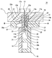
本実施形態に係る流量センサは、流体との伝熱を利用して、流体の流量を検出するものである。本実施形態では、その一例として、車両の内燃機関(図示せず)に吸入される空気流(吸気流)の流量を検出するために、図1に示すように、その一部が吸気管101内に突出するように、プラグイン方式によって着脱可能に取り付けられた流量センサ10の例を示す。なお、符号100は、吸気管101に形成された、流体(空気)が流れる主通路を示す。
(1st Embodiment)
The flow rate sensor according to the present embodiment detects the flow rate of a fluid using heat transfer with the fluid. In the present embodiment, as an example, in order to detect the flow rate of an air flow (intake flow) taken into an internal combustion engine (not shown) of the vehicle, as shown in FIG. 1 shows an example of a
先ず、図1及び図2を用いて、流量センサ10の概略構成を説明する。
First, a schematic configuration of the
この流量センサ10は、要部として、センシング部20を有する流量検出チップ11と、回路チップ12と、回路チップ12を支持する搭載部23aを含むリードフレーム13と、回路チップ12などを封止する1次樹脂成形体14と、を備えている。さらに、流体を主通路100からセンシング部20に導く副通路15を形成する副通路形成部材16と、上記した各要素を吸気管101に取り付けるための2次樹脂成形体17と、を備えている。なお、1次樹脂成形体14が、特許請求の範囲に記載の樹脂成形体に相当する。
The
流量検出チップ11としては、周知構成のものを採用することができる。この流量検出チップ11は、例えばシリコン基板からなり、表面11a側に薄肉部としてのメンブレンが形成されている。なお、メンブレンの直下部分は、エッチングにより除去され、裏面11bに開口する空洞部となっている。センシング部20は、少なくとも一部がメンブレンに形成されており、センシング部20を構成する後述のヒータ抵抗40や流量検出抵抗41a〜41d(図6参照)も、メンブレンに形成されている。この流量検出チップ11は、裏面11b側を1次樹脂成形体14の後述する支持部14bに対向させた状態で、接着層21を介して1次樹脂成形体14に固定されている。なお、表面11aが特許請求の範囲に記載の第1主面、裏面11bが特許請求の範囲に記載の第2主面に相当する。
As the flow
回路チップ12としても、周知構成のもの、例えばシリコンなどの半導体基板に素子が形成されたものを採用することができる。この回路チップ12には、流量検出チップ11から出力された検出信号の処理回路が形成されている。また、センシング部20を構成するヒータ抵抗40などの電源回路や、ヒータ抵抗40の通電状態を制御する回路などが形成されている。この回路チップ12は、接着層22を介して、リードフレーム13の搭載部23aに固定されている。
As the
リードフレーム13は、銅などからなる金属板の表面に耐食性加工(例えばメッキ)を施してなり、搭載部23aとリード23bを有している。搭載部23aは、上記の通り、回路チップ12を支持する機能を果たしている。回路チップ12は、リードフレーム13(搭載部23a)の表面13aに固定されている。さらに本実施形態では、搭載部23aが、回路チップ12に形成された回路と、流量検出チップ11に形成されたセンシング部20などとの電気的な接続を中継する機能を果たしている。この搭載部23aと回路チップ12の図示しないパッドとが、ワイヤ24を介して電気的に接続され、同じく搭載部23aと流量検出チップ11の図示しないパッドとが、ワイヤ25を介して電気的に接続されている。このように、回路チップ12は、ワイヤ24、搭載部23a、及びワイヤ25を介して、流量検出チップ11と電気的に接続されている。なお、表面13aが特許請求の範囲に記載の搭載面に相当する。
The
一方、リード23bは、外部接続端子としての機能を果たすものであり、例えば、該リード23bを介して、回路チップ12の処理回路で処理された信号が、外部機器に出力されるようになっている。リード23bは、ワイヤ26を介して回路チップ12と電気的に接続されている。このリード23bは、1次樹脂成形体14の成形後、タイバーカットにより、搭載部23aとは電気的に分離されている。なお、本実施形態では、吸気管101の主通路100内に配置されない位置を、タイバーカットの位置としており、タイバーカット部分は、2次樹脂成形体17により封止されている。
On the other hand, the lead 23b functions as an external connection terminal. For example, a signal processed by the processing circuit of the
1次樹脂成形体14は、少なくとも回路チップ12及び該回路チップ12と他部材とを電気的に接続する部分、本実施形態ではワイヤ24,26を保護するものである。この1次樹脂成形体14は、例えばエポキシ樹脂を用いてトランスファー法により、リードフレーム13、リードフレーム13に固定された回路チップ12、及びワイヤ24,26と一体的に成形されている。
The primary resin molded
1次樹脂成形体14のうち、図2に示す被覆部14aが、回路チップ12とワイヤ24,26を被覆・保護する機能を果たす部分となっている。また、1次樹脂成形体14が、被覆部14aだけでなく、流量検出チップ11を支持する支持部14bを有している。この支持部14bは被覆部14aと一体的に形成されている。流量検出チップ11は、1次樹脂成形体14の形成後、支持部14bに、接着層21を介して固定される。支持部14bは、流量検出チップ11の厚さ方向において、流量検出チップ11が回路チップ12とほぼ同じ位置となるような、流量検出チップ11の搭載面を有して形成されている。
In the primary resin molded
なお、搭載部23aのうち、後述する孔部28により露出された裏面13bの一部と、表面13aの一部が、1次樹脂成形体14から露出されている。そして、流量検出チップ11に一端が接続されたワイヤ25の他端が、搭載部23aの表面13aにおける露出部分に接続されている。このワイヤ25は、ポッティング等により設けられた例えばゲルからなる保護部材27によって被覆されている。保護部材27は、流量検出チップ11の表面11aのうち、ワイヤ25が接続されたパッドの周辺部分のみを被覆しており、センシング部20は、保護部材27及び1次樹脂成形体14から露出されている。この保護部材27は、支持部14bに流量検出チップ11を固定し、ワイヤ25により、流量検出チップ11と搭載部23aとを接続した後、配置される。
In the mounting
一方、リード23bは、ワイヤ26が接続された一端の周辺のみが1次樹脂成形体14によって被覆されており、それ以外の部分は、1次樹脂成形体14から外部に突出している。
On the other hand, the lead 23b is covered only with the primary resin molded
副通路形成部材16は、主通路100を流れる流体を、流量検出チップ11のセンシング部20に導く副通路15を形成している部材である。この副通路形成部材16は、PBTやPPSなどの樹脂を成形してなり、ケース30とカバー31の2つから成り立っている。ケース30は、略矩形平板状とされた基部30aと、基部30aの一面に立設された平板に、通路なす溝が形成された副通路形成部30bと、を有している。ケース30にカバー31が組み付けられると、副通路形成部30bとカバー31とにより、副通路15が形成されるようになっている。
The sub
副通路形成部材16のうち、少なくとも副通路形成部30b及びカバー31、すなわち副通路15の形成部分は、主通路100を形成する吸気管101に形成された取り付け孔より、吸気管101内に挿入配置される。本実施形態では、図1に示すように、基部30aにおける副通路形成部30bと反対の面が、吸気管101の外面と面一となるように配置される。
Of the
ケース30の基部30aには、流量検出チップ11のセンシング部20を副通路15内に挿入配置させるための差込口32が形成されている。この差込口32は、平板状をなす基部30aを、厚さ方向に貫通して形成されている。また、差込口32には、1次構造体18が差し込まれる。この1次構造体18は、流量検出チップ11、回路チップ12、及びリードフレーム13が、1次樹脂成形体14及び接着層21,22により一体化されたものである。
The base 30 a of the
2次樹脂成形体17は、流量センサ10を吸気管101に取り付けるための部分であり、図1及び図2に示すように、1次樹脂成形体14の被覆部14a及び副通路形成部材16の基部30aに密着している。また、2次樹脂成形体17は、リード23bの一部を被覆している。この2次樹脂成形体17は、1次構造体18を副通路形成部材16の差込口32に挿入した状態で、1次構造体18及び副通路形成部材16と一体的に樹脂成形することで形成される。
The secondary resin molded
この2次樹脂成形体17は、平板状の基部17aと、基部17aにおける副通路形成部材16側と反対の面に立設された環状の壁部17bを有している。上記したリード23bの一方の端部は、壁部17bが取り囲む空間に突出しており、外部機器との接続が可能となっている。また、2次樹脂成形体17の基部17aと副通路形成部材16の基部30aとのお互いの対向面は、基部17a側が基部30a側を内包する関係となっている。このため、流量センサ10を吸気管101の取り付け穴に挿入する際に、副通路形成部材16の基部30aまでが取り付け穴に挿入され、2次樹脂成形体17の基部17aは、その縁部が吸気管101の外面に接触し、挿入方向における位置が決定されるようになっている。
The secondary resin molded
次に、上記した流量センサ10の製造方法の一例を簡単に説明する。
Next, an example of a method of manufacturing the above-described
先ず、リードフレーム13の表面13aにおいて、搭載部23aの所定位置に、接着層22を介して回路チップ12を固定する。そして、ワイヤ24,26を接続する。次いで、1次樹脂成形体14を形成した後、リードフレーム13の図示しないタイバーをカットするとともに、支持部14bに、接着層21を介して流量検出チップ11を固定する。そして、ワイヤ25を接続した後、該ワイヤ25を保護部材27により被覆する。次いで、別途準備したケース30に対し、副通路15にセンシング部20が位置するように、差込口32を形成する部分に1次構造体18を配置する。そして、カバー31をケース30に組み付けて副通路形成部材16を形成する。このとき、シール材を用いて、1次構造体18を副通路形成部材16に固定する。なお、副通路形成部材16を形成した後、差込口32から1次構造体18を挿入しても良い。最後に、1次構造体18と副通路形成部材16の一体物をインサート部品として、2次樹脂成形体17を成形する。以上により、図2に示す流量センサ10を得ることができる。
First, the
次に、流量センサ10の特徴部分の構成と効果について、図2及び図3を用いて説明する。
Next, the configuration and effect of the characteristic portion of the
図2及び図3に示すように、1次樹脂成形体14に、孔部28が形成されている。この孔部28は、回路チップ12が固定されたリードフレーム13の部分、すなわち搭載部23aの裏面13bの一部を底とし、1次樹脂成形体14の外面に開口している。すなわち、孔部28により、搭載部23aの裏面13bの一部が、1次樹脂成形体14の外部に露出されている。そして、孔部28を通じて、搭載部23aの裏面13bの一部が流体に晒されるようになっている。なお、この孔部28は、1次樹脂成形体14の成形時に形成される。また、本実施形態では、図2に示すように、搭載部23aにおいて、回路チップ12が配置された側の端部と反対の端部近傍が、露出されている。
As shown in FIGS. 2 and 3, a
本実施形態では、副通路形成部材16を構成するケース30の基部30aに、差込口32に1次構造体18を挿入配置した状態で孔部28と連通する開口部33が形成されている。この開口部33は、差込口32に繋がっており、1次構造体18を差込口32に挿入配置すると、開口部33が孔部28と連通するようになっている。一方、開口部33は、副通路形成部材16を形成した状態で、基部30aにおけるカバー31側の面にも開口し、この開口部分から、主通路100を流れる流体が導入可能となっている。
In the present embodiment, an
また、孔部28により露出された搭載部23aの露出部分の面積が、搭載部23aの側面のうち、主通路100を流れる流体の流れ方向に対する端面の面積よりも大きくなっている。なお、本実施形態では、該端面の面積が図2に示す搭載部23aの断面積とほぼ一致している。
The area of the exposed portion of the mounting
このように、本実施形態に係る流量センサ10によれば、1次樹脂成形体14に孔部28が形成されており、この孔部28によってリードフレーム13における搭載部23aの裏面13bの一部が、1次樹脂成形体14の外部に露出されている。したがって、裏面13bの露出部分を、外部雰囲気、すなわち流体に晒すことができる。換言すれば、裏面13bの露出部分に流体を当てることができる。これにより、回路チップ12の動作による熱を、流体に逃がすことができる。すなわち、放熱性を向上することができる。
As described above, according to the
また、裏面13bは、タイバーカット後の切断面ではないため、メッキなどの耐食性加工が施された状態となっている。したがって、タイバーカット後にコーティングが不要であり、製造工程を増やさずに耐環境性を向上することができる。換言すれば、製造工程を増やさずに、1次樹脂成形体14の封止性を保って、回路チップ12などの信頼性低下を抑制することができる。
Also, since the
また、主通路100を流れる流体の流れ方向に対する搭載部23aの端面の面積よりも、搭載部23aの露出部分の面積のほうが大きくなっている。これによれば、露出部分の面積が、搭載部23aの端面の面積以下とされる構造に較べて、放熱性を向上することができる。
The area of the exposed portion of the mounting
(第2実施形態)
本実施形態において、上記実施形態に示した流量センサ10と共通する部分についての説明は割愛する。本実施形態の第1の特徴は、図4に示すように、リードフレーム13における搭載部23aの裏面13bにおいて、回路チップ12とオーバーラップするオーバーラップ領域29の少なくとも一部が、孔部28により、1次樹脂成形体14の外部に露出されていることにある。第2の特徴は、オーバーラップ領域29の全域が、孔部28により、1次樹脂成形体14の外部に露出されていることにある。それ以外の構成は、第1実施形態に示した流量センサ10と同じである。なお、オーバーラップ領域29とは、投影領域とも言い換えることができる。
(2nd Embodiment)
In the present embodiment, the description of the portions common to the
このように、本実施形態では、オーバーラップ領域29の少なくとも一部が、孔部28により、1次樹脂成形体14の外部に露出されている。したがって、リードフレーム13の搭載部23aのうち、特に回路チップ12に近い部分が流体に晒される。換言すれば、熱源に近い位置に流体を当てることができる。このため、回路チップ12の動作による熱を、効率よく流体に逃すことができる。すなわち、放熱性をより向上することができる。
As described above, in the present embodiment, at least a part of the
特に本実施形態では、図4に示すように、オーバーラップ領域29の全域が、孔部28により露出されており、オーバーラップ領域29の全域が流体に晒されるため、放熱性をさらに向上することができる。
In particular, in this embodiment, as shown in FIG. 4, the entire area of the
(第3実施形態)
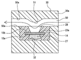
本実施形態において、上記実施形態に示した流量センサ10と共通する部分についての説明は割愛する。本実施形態の特徴は、図5に示すように、流量検出チップ11及び回路チップ12が、雰囲気温度を検出する温度検出部としての測温抵抗42,43をそれぞれ有している。その上で、図6に示すように、副通路15と孔部28とが互いに連通していることにある。なお、図5に示す回路図は、実際の回路構成のうち、特徴部分のみを抽出して図示している。実際は、ヒータ抵抗40の通電状態を制御する回路などが存在するが、周知であり、図示を省略する。
(Third embodiment)
In the present embodiment, the description of the portions common to the
図5に示すように、流量検出チップ11の薄肉部には、センシング部20を構成するヒータ抵抗40及び流量検出抵抗41a〜41が形成されている。ヒータ抵抗40は、自身の発熱により、主通路100を流れる流体の流れ方向に温度分布を形成する機能を果たす。
As shown in FIG. 5, a
平面長方形の流量検出チップ11は、自身の短手方向が、流量センサ10が吸気管101に取り付けられた状態で、主通路100を流れる流体の流れに沿う方向となっている。そして、ヒータ抵抗40は、流量検出チップ11の短手方向において、流量検出チップ11の薄肉部の中心に位置しており、短手方向において、ヒータ抵抗40を挟んで等距離に、流量検出抵抗41b,41cが配置されている。なお、流量検出抵抗41bが、流体の通常時の流れにおいて上流側、流量検出抵抗41cが下流側となっている。また、ヒータ抵抗40を挟んで等距離、且つ、流量検出抵抗41b,41cよりもヒータ抵抗40に対して遠い位置に、流量検出抵抗41a,41dが配置されている。なお、流量検出抵抗41aが、流体の通常時の流れにおいて上流側、流量検出抵抗41dが下流側となっている。
The
各流量検出抵抗41a〜41は、同じ材料を用いて同じパターン形状で形成されている。すなわち、いずれも同じ温度係数を有するとともに、同じ温度で同じ抵抗値を示す。そして、4つの流量検出抵抗41a〜41dによりフルブリッジ回路が構成されている。具体的には、流量検出抵抗41a,41cの接続点に、回路チップ12に形成された電源回路44が接続されている。また、流量検出抵抗41d,41bの接続点に、グランドが接続されている。そして、流量検出抵抗41a,41dの接続点の電位と、流量検出抵抗41c,41bの接続点の電位が、回路チップ12に形成された信号処理回路46に入力されるようになっている。なお、ヒータ抵抗40は、上記した電源回路44とグランドとの間に接続されている。また、電源回路44は、定電圧を供給する。
The flow
また、流量検出チップ11には、外部雰囲気の温度を検出するための第1測温抵抗42が形成されている。この第1測温抵抗42は、ヒータ抵抗40の熱の影響を受けないように、流量検出チップ11の長手方向において、ヒータ抵抗40と離れた位置に形成されている。一方、回路チップ12には、外部雰囲気の温度を検出するための第2測温抵抗43が形成されている。これら2つの測温抵抗42,43が、特許請求の範囲に記載の温度検出部に相当する。
Further, the flow
2つの測温抵抗42,43は、図5に示すように、電源回路44とグランドとの間に、第1測温抵抗42をグランド側として直列配置されている。そして、第1測温抵抗42と第2測温抵抗43の接続点の電位(中点電圧)が、回路チップ12に形成された温度補正回路45に入力されるようになっている。これら2つの測温抵抗42,43は、異なる温度係数を有する材料を用いて形成されている。このように温度係数が異なるため、雰囲気の温度変化により測温抵抗42,43の中点電圧が変化する。温度補正回路45は、2つの測温抵抗42,43の中点電圧の値を雰囲気温度に換算し、この換算温度に基づく信号を信号処理回路46に出力する。信号処理回路46は、フルブリッジ回路から出力された信号を、上記換算温度に基づく信号を用いて補正する。そして、補正された信号は、リード23bを介して外部に出力される。
As shown in FIG. 5, the two
本実施形態では、図6に示すように、副通路形成部材16に形成された副通路15と、1次樹脂成形体14に形成された孔部28とが、互いに連通している。したがって、副通路15を流れる流体の一部が、開口部33を介して孔部28に導入され、搭載部23aの裏面13bの露出部位が、流体に晒される。このため、回路チップ12の動作による熱を、流体に逃すことができる。すなわち、放熱性を向上することができる。
In the present embodiment, as shown in FIG. 6, the sub-passage 15 formed in the
また、孔部28と副通路15が連通することで、回路チップ12と流量検出チップ11の温度差が小さくなる。すなわち、2つの測温抵抗42,43がほぼ同じ外部雰囲気の温度を検出できるようになる。このように、回路チップ12と流量検出チップ11の温度をほぼ同じにすることで、実際の温度と測温抵抗42,43の中点電圧とのずれが小さくなり、温度検出の精度を向上することができる。そして、中点電圧に基づく温度補正の精度を向上することができる。
In addition, the communication between the
(第4実施形態)
本実施形態において、上記実施形態に示した流量センサ10と共通する部分についての説明は割愛する。本実施形態の第1の特徴は、図7(a),(b)に示すように、副通路形成部材16が、自身の外面に、主通路100を流れる流体の流れ方向に沿って形成された溝部50を有している。そして、この溝部50が、孔部28と連通していることにある。
(Fourth embodiment)
In the present embodiment, the description of the portions common to the
図7(a)は、ケース30にカバー31を組み付ける前であって、上記した1次構造体18をケース30に組み付ける前の状態を示している。図7に示す例では、ケース30の基部30aのうち、副通路形成部30bが立設された側の面に、吸気管101に配置された状態で、主通路100における流体の流れ方向に沿うように、溝部50が形成されている。この溝部50は、その長手方向中央において、差込口32と連通している。溝部50は、基部30aのうち、副通路形成部30bが立設された側の面に対し、所定深さを有して形成されている。したがって、ケース30の差込口32に1次構造体18を挿入配置し、カバー31をケース30に組み付けた状態で、孔部28が溝部50と連通する。また、図7(b)に示すように、溝部50に沿って流体が流れるため、溝部50を流れる流体の一部が、溝部50に連通する孔部28に導入される。
FIG. 7A shows a state before the
このように、図7(a),(b)に例示する流量センサ10によれば、主通路100を流れる流体が、溝部50から孔部28内に導入されやすくなる。そして、裏面13bにおける搭載部23aの露出部分に流体を当てることができる。これにより、回路チップ12の動作による熱を、流体に逃がすことができる。すなわち、放熱性を向上することができる。
As described above, according to the
また、第2の特徴は、図8に示すように、副通路形成部材16において、溝部50の側壁50aのうち、1次樹脂成形体14の外面に開口する孔部28との対向部分に、孔部28に向けて突出する突起部51を有することにある。図8に示す例では、突起部51が、流体の流れ方向において、孔部28の開口部の中央を頂点とする弧状をなしている。溝部50を流れる流体は側壁50aに沿って流れるため、図8に示すように、突起部51に沿って流れる流体が、孔部28に導入されやすくなる。
The second feature is that, as shown in FIG. 8, in the
このように、図8に例示する流量センサ10によれば、突起部51の存在により、溝部50を流れる流体が、孔部28に導入されやすくなる。すなわち、裏面13bにおける搭載部23aの露出部分に流体が当たり易くなる。これにより、放熱性をさらに向上することができる。
As described above, according to the
以上、本発明の好ましい実施形態について説明したが、本発明は上述した実施形態になんら制限されることなく、本発明の主旨を逸脱しない範囲において、種々変形して実施することが可能である。 As described above, the preferred embodiments of the present invention have been described. However, the present invention is not limited to the above-described embodiments, and can be variously modified and implemented without departing from the gist of the present invention.
本実施形態では、流量検出チップ11が、1次樹脂成形体14の支持部14bに固定され、ワイヤ25が保護部材27により被覆される例を示した。しかしながら、それ以外の構成も可能である。例えば、リードフレーム13に流量検出チップが固定された構成としても良い。また、流量検出チップと回路チップが、リードフレームを介さずにワイヤによって電気的に接続され、該ワイヤが1次樹脂成形体14により被覆される構成としても良い。すなわち、搭載部23aが、流量検出チップ11と回路チップ12の電気的な中継機能を果たさない構成を採用することもできる。
In the present embodiment, an example has been described in which the flow
10・・・流量センサ、11・・・流量検出チップ、11a・・・表面(第1主面)、11b・・・裏面(第2主面)、12・・・回路チップ、13・・・リードフレーム、13a・・・表面(搭載面)、13b・・・裏面、14・・・1次樹脂成形体(樹脂成形体)、15・・・副通路、16・・・副通路形成部材、17・・・2次樹脂成形体、20・・・センシング部、23a・・・搭載部、28・・・孔部、29・・・オーバーラップ領域、50・・・溝部、50a・・・側壁、51・・・突起部、100・・・主通路、101・・・吸気管 Reference numeral 10: flow sensor, 11: flow detection chip, 11a: front surface (first main surface), 11b: back surface (second main surface), 12: circuit chip, 13 ... Lead frame, 13a front surface (mounting surface), 13b back surface, 14 primary resin molded body (resin molded body), 15 sub-passage, 16 sub-passage forming member, 17 ... secondary resin molded body, 20 ... sensing part, 23a ... mounting part, 28 ... hole, 29 ... overlap area, 50 ... groove, 50a ... side wall , 51: Projection, 100: Main passage, 101: Intake pipe
Claims (1)
前記副通路に導かれた流体の流量を検出するセンシング部(20)が形成された流量検出チップ(11)と、
前記流量検出チップ(11)と電気的に接続された回路チップ(12)と、
前記回路チップ(12)が搭載された搭載面(13a)及び該搭載面と反対の裏面(13b)を有し、前記搭載面(13a)における前記回路チップ(12)とは異なる位置に前記流量検出チップ(11)が接続されたリードフレーム(13,23a,23b)と、
前記リードフレーム(13,23a,23b)における搭載面及び裏面の両側に配置され、前記センシング部(20)を露出させつつ、前記回路チップ(12)を封止する樹脂成形体(14)と、を備え、
前記樹脂成形体(14)は、前記リードフレーム(13,23a)の裏面(13b)の一部が底をなし、該樹脂成形体(14)の外面に開口する孔部(28)を有しており、
前記リードフレーム(13,23a)は、前記孔部(28)を介して、前記副通路(15)を流れる流体に晒され、
前記孔部(28)の開口は、前記回路チップ(12)の直下とは異なる位置に配置され、前記リードフレーム(13,23a)から離れるにつれて広くなっており、
前記リードフレーム(13,23a,23b)の切断面は前記流体に晒されないように前記樹脂部材(16,17)によって前記流体とは隔離され、前記孔部(28)から前記切断面が露出しないように前記孔部(28)が設けられていることを特徴とする流量センサ。 A resin member (16, 17) having a sub-passage (15) for guiding a fluid flowing through the main passage (100) to the inside, and attached to a pipe member (101) constituting the main passage;
A flow rate detection chip (11) provided with a sensing unit (20) for detecting a flow rate of the fluid guided to the auxiliary passage ;
A circuit chip (12) electrically connected to the flow rate detection chip (11);
Said circuit having a chip (12) is mounted on the mounting surface (13a) and said mounting surface opposite to the back surface (13b), wherein the position different from the circuit chip definitive on the mounting surface (13a) (12) A lead frame (13 , 23a, 23b ) to which the flow rate detection chip (11) is connected ;
A resin molded body (14) disposed on both sides of a mounting surface and a back surface of the lead frame (13 , 23a, 23b ) to seal the circuit chip (12) while exposing the sensing portion (20); With
The resin molded body (14) has a hole (28) that is formed on a part of the back surface (13b) of the lead frame ( 13, 23a) as a bottom and opens on the outer surface of the resin molded body (14). And
The lead frame (13, 23a) is exposed to the fluid flowing through the sub-passage (15) through the hole (28) ,
Opening of the hole (28), the arranged positions different from the right under the circuit chip (12), and Tsu a wider as distance from the lead frame (13,23A),
The cut surfaces of the lead frames (13, 23a, 23b) are isolated from the fluid by the resin members (16, 17) so as not to be exposed to the fluid, and the cut surfaces are not exposed from the holes (28). A flow sensor characterized in that the hole (28) is provided as described above .
Priority Applications (1)
| Application Number | Priority Date | Filing Date | Title |
|---|---|---|---|
| JP2018175280A JP6658833B2 (en) | 2018-09-19 | 2018-09-19 | Flow sensor |
Applications Claiming Priority (1)
| Application Number | Priority Date | Filing Date | Title |
|---|---|---|---|
| JP2018175280A JP6658833B2 (en) | 2018-09-19 | 2018-09-19 | Flow sensor |
Related Parent Applications (1)
| Application Number | Title | Priority Date | Filing Date |
|---|---|---|---|
| JP2017112958A Division JP6406396B2 (en) | 2017-06-07 | 2017-06-07 | Flow sensor |
Publications (2)
| Publication Number | Publication Date |
|---|---|
| JP2018197764A JP2018197764A (en) | 2018-12-13 |
| JP6658833B2 true JP6658833B2 (en) | 2020-03-04 |
Family
ID=64662611
Family Applications (1)
| Application Number | Title | Priority Date | Filing Date |
|---|---|---|---|
| JP2018175280A Active JP6658833B2 (en) | 2018-09-19 | 2018-09-19 | Flow sensor |
Country Status (1)
| Country | Link |
|---|---|
| JP (1) | JP6658833B2 (en) |
Families Citing this family (2)
| Publication number | Priority date | Publication date | Assignee | Title |
|---|---|---|---|---|
| US11143535B2 (en) * | 2017-09-05 | 2021-10-12 | Hitachi Automotive Systems, Ltd. | Thermal-type flowmeter |
| WO2020080214A1 (en) | 2018-10-19 | 2020-04-23 | 三菱瓦斯化学株式会社 | Thermosetting resin composition, prepreg, resin sheet, metal foil clad laminated sheet, and printed wiring board |
-
2018
- 2018-09-19 JP JP2018175280A patent/JP6658833B2/en active Active
Also Published As
| Publication number | Publication date |
|---|---|
| JP2018197764A (en) | 2018-12-13 |
Similar Documents
| Publication | Publication Date | Title |
|---|---|---|
| US10371552B2 (en) | Physical quantity detection device | |
| US7219544B2 (en) | Thermal-type flow rate sensor and manufacturing method thereof | |
| US20060112763A1 (en) | Flow rate measuring apparatus | |
| EP2789994B1 (en) | Airflow measuring apparatus | |
| US9945706B2 (en) | Thermal-type air flow meter | |
| JP6658833B2 (en) | Flow sensor | |
| JP2006010426A (en) | Sensor device and its manufacturing method | |
| WO2017110541A1 (en) | Air flow rate measurement device | |
| JP6406396B2 (en) | Flow sensor | |
| JP5870748B2 (en) | Flow sensor | |
| JP6043833B2 (en) | Thermal flow meter | |
| JP6134840B2 (en) | Thermal flow meter | |
| JP6156523B2 (en) | Flow sensor | |
| JP6458104B2 (en) | Thermal flow meter | |
| US10900820B2 (en) | Air flow rate measurement device having a segmented board portion at an upstream side to suppress flow disturbances | |
| JP2002318146A (en) | Air flow rate measuring device and its manufacturing method | |
| JP6215502B2 (en) | Thermal flow meter | |
| JP7317103B2 (en) | Physical quantity measuring device | |
| JP2017150929A (en) | Physical quantity detector | |
| JP6602744B2 (en) | Sensor device and manufacturing method thereof | |
| JP2019168303A (en) | Temperature sensor |
Legal Events
| Date | Code | Title | Description |
|---|---|---|---|
| A521 | Request for written amendment filed |
Free format text: JAPANESE INTERMEDIATE CODE: A523 Effective date: 20181011 |
|
| A621 | Written request for application examination |
Free format text: JAPANESE INTERMEDIATE CODE: A621 Effective date: 20181011 |
|
| A131 | Notification of reasons for refusal |
Free format text: JAPANESE INTERMEDIATE CODE: A131 Effective date: 20191015 |
|
| A521 | Request for written amendment filed |
Free format text: JAPANESE INTERMEDIATE CODE: A523 Effective date: 20191211 |
|
| TRDD | Decision of grant or rejection written | ||
| A01 | Written decision to grant a patent or to grant a registration (utility model) |
Free format text: JAPANESE INTERMEDIATE CODE: A01 Effective date: 20200107 |
|
| A61 | First payment of annual fees (during grant procedure) |
Free format text: JAPANESE INTERMEDIATE CODE: A61 Effective date: 20200120 |
|
| R151 | Written notification of patent or utility model registration |
Ref document number: 6658833 Country of ref document: JP Free format text: JAPANESE INTERMEDIATE CODE: R151 |
|
| R250 | Receipt of annual fees |
Free format text: JAPANESE INTERMEDIATE CODE: R250 |
|
| R250 | Receipt of annual fees |
Free format text: JAPANESE INTERMEDIATE CODE: R250 |