JP6651834B2 - Voltage-controlled oscillator, electronic device, and moving object - Google Patents
Voltage-controlled oscillator, electronic device, and moving object Download PDFInfo
- Publication number
- JP6651834B2 JP6651834B2 JP2015247052A JP2015247052A JP6651834B2 JP 6651834 B2 JP6651834 B2 JP 6651834B2 JP 2015247052 A JP2015247052 A JP 2015247052A JP 2015247052 A JP2015247052 A JP 2015247052A JP 6651834 B2 JP6651834 B2 JP 6651834B2
- Authority
- JP
- Japan
- Prior art keywords
- voltage
- variable capacitance
- temperature compensation
- sensitivity
- capacitance element
- Prior art date
- Legal status (The legal status is an assumption and is not a legal conclusion. Google has not performed a legal analysis and makes no representation as to the accuracy of the status listed.)
- Active
Links
Images


Description
本発明は、制御電圧に従って発振周波数が制御される電圧制御発振器に関する。さらに、本発明は、そのような電圧制御発振器を用いた電子機器及び移動体等に関する。 The present invention relates to a voltage controlled oscillator whose oscillation frequency is controlled according to a control voltage. Further, the present invention relates to an electronic device, a moving object, and the like using such a voltage controlled oscillator.
例えば、温度補償型水晶発振器(TCXO)において、外部から印加される制御電圧に従って発振周波数が制御される機能を有する場合には、そのような機能を有さない場合と比較して、精度が劣化する傾向にあった。しかしながら、近年においては高精度化の要求が高まり、外部から印加される制御電圧に従って発振周波数が制御される機能を有する発振器に対しても、そのような機能を有さない発振器と同等の精度が求められるようになっている。 For example, when a temperature-compensated crystal oscillator (TCXO) has a function of controlling the oscillation frequency according to a control voltage applied from the outside, the accuracy is deteriorated as compared with a case without such a function. I tended to. However, in recent years, the demand for higher accuracy has increased, and even for an oscillator having a function of controlling the oscillation frequency according to a control voltage applied from the outside, the same accuracy as an oscillator having no such function is provided. It has become required.
関連する技術として、特許文献1には、入力端子に印加される制御電圧に応じて発振周波数を変化させるAFC(Automatic Frequency Control)回路を備えた温度補償型水晶発振器が開示されている。一般に、温度補償電圧は、AFC回路に入力される制御電圧が圧電振動子において基本周波数で発振する基準電圧値である場合に、最も温度補償が有効に行われるように調整されている。 As a related technique, Patent Document 1 discloses a temperature-compensated crystal oscillator including an AFC (Automatic Frequency Control) circuit that changes an oscillation frequency according to a control voltage applied to an input terminal. Generally, the temperature compensation voltage is adjusted so that the temperature compensation is performed most effectively when the control voltage input to the AFC circuit is a reference voltage value that oscillates at the fundamental frequency in the piezoelectric vibrator.
従って、AFC回路に基準電圧値と異なる制御電圧が入力された場合には、発振回路側の等価容量値が変化するので、必要とされる温度補償電圧が、基本周波数を基準とする温度補償電圧とは異なった値になる。その結果、温度補償が不足したり、あるいは、温度補償が効き過ぎてしまうといった現象が起こり、精度の高い温度補償が実現できないという問題を有していた。 Therefore, when a control voltage different from the reference voltage value is input to the AFC circuit, the equivalent capacitance value on the oscillation circuit side changes, and the required temperature compensation voltage becomes the temperature compensation voltage based on the fundamental frequency. Will be different. As a result, a phenomenon occurs in which the temperature compensation is insufficient or the temperature compensation is too effective, and there is a problem that highly accurate temperature compensation cannot be realized.
この問題を解決するために、特許文献1の図1には、発振回路12と、第1温度補償電圧発生回路30と、エンコーダー38と、第2温度補償電圧発生回路44と、AFC回路54とを有する温度補償型発振回路10が示されている。発振回路12に含まれているインバーターの入力端子及び出力端子の各々には、第1可変容量素子16と、第2可変容量素子18とが並列に接続されている。
In order to solve this problem, FIG. 1 of Patent Document 1 discloses an
第1温度補償電圧発生回路30は、温度補償電圧を第1可変容量素子16の第1の端子及び第2温度補償電圧発生回路44に出力する。AFC回路54は、入力端子に印加される制御電圧に応じて、発振回路12の発振周波数を調整する出力電圧を第2可変容量素子18の第2の端子に出力すると共に、増幅度補正信号を第2温度補償電圧発生回路44に出力する。第2温度補償電圧発生回路44は、温度補償電圧を増幅度補正信号に基づいて増幅した補助温度補償電圧を第1可変容量素子16の第2の端子に出力する。
The first temperature compensation
従って、第1可変容量素子16には、温度補償電圧が印加されると共に、補助温度補償電圧が印加されることになる。それにより、第1可変容量素子16を感度のリニアリティが良好な状態で使用することが可能な制御電圧の範囲が制限されてしまう。また、第1可変容量素子16は、温度補償のために高い感度を有しているので、制御電圧に含まれているノイズ成分によって発振信号の位相ノイズが増加するおそれがある。 Accordingly, the temperature compensation voltage is applied to the first variable capacitance element 16, and the auxiliary temperature compensation voltage is applied to the first variable capacitance element 16. As a result, the range of the control voltage at which the first variable capacitance element 16 can be used with good sensitivity linearity is limited. In addition, since the first variable capacitance element 16 has high sensitivity for temperature compensation, the phase noise of the oscillation signal may increase due to a noise component included in the control voltage.
そこで、上記の点に鑑み、本発明の第1の目的は、制御電圧に従って発振周波数が制御される電圧制御発振器において、可変容量素子を感度のリニアリティが良好な状態で使用することが可能な制御電圧の範囲を拡大することである。また、本発明の第2の目的は、制御電圧に従って発振周波数が制御される電圧制御発振器において、発振信号の位相ノイズを低減することである。さらに、本発明の第3の目的は、そのような電圧制御発振器を用いた電子機器及び移動体等を提供することである。 In view of the above, a first object of the present invention is to provide a voltage-controlled oscillator whose oscillation frequency is controlled according to a control voltage, in which a variable capacitance element can be used in a state in which the sensitivity linearity is good. It is to expand the range of the voltage. A second object of the present invention is to reduce the phase noise of an oscillation signal in a voltage controlled oscillator whose oscillation frequency is controlled according to a control voltage. Further, a third object of the present invention is to provide an electronic device, a moving object, and the like using such a voltage controlled oscillator.
以上の課題の少なくとも一部を解決するために、本発明の第1の観点に係る電圧制御発振器は、振動体の第1の電極と第2の電極とに接続されて発振動作を行う発振部と、振動体の第1又は第2の電極に接続されて発振周波数を調節する第1の可変容量素子と、温度センサーから出力される検出信号に従って、第1の可変容量素子の容量値を制御する第1の温度補償電圧を生成する第1の温度補償電圧生成回路と、振動体の第1又は第2の電極に接続されて発振周波数を調節する第2の可変容量素子と、周波数制御信号に従って、第2の可変容量素子の容量値を制御する周波数制御電圧を生成する周波数制御電圧生成回路と、振動体の第1又は第2の電極に接続されて発振周波数を調節する第3の可変容量素子と、周波数制御電圧の変化によって生じる温度補償量の変化を補正するために、第1の温度補償電圧及び周波数制御電圧に基づいて、第3の可変容量素子の容量値を制御する第2の温度補償電圧を生成する第2の温度補償電圧生成回路とを備える。 In order to solve at least a part of the above-described problems, a voltage-controlled oscillator according to a first aspect of the present invention includes an oscillation unit that is connected to a first electrode and a second electrode of a vibrating body and performs an oscillation operation A first variable capacitance element connected to the first or second electrode of the vibrating body to adjust the oscillation frequency, and a capacitance value of the first variable capacitance element is controlled according to a detection signal output from the temperature sensor. A first temperature compensation voltage generating circuit for generating a first temperature compensation voltage to be applied, a second variable capacitance element connected to the first or second electrode of the vibrating body to adjust the oscillation frequency, and a frequency control signal A frequency control voltage generating circuit for generating a frequency control voltage for controlling the capacitance value of the second variable capacitance element, and a third variable for connecting to the first or second electrode of the vibrator to adjust the oscillation frequency. The capacitance element and the frequency control voltage change A second temperature compensation voltage for controlling a capacitance value of the third variable capacitance element based on the first temperature compensation voltage and the frequency control voltage in order to correct a change in the temperature compensation amount caused by the second temperature compensation voltage. And a temperature compensation voltage generation circuit.
本発明の第1の観点によれば、第1の温度補償電圧に従って発振周波数を調節する第1の可変容量素子、及び、周波数制御電圧に従って発振周波数を調節する第2の可変容量素子とは別個に、第2の温度補償電圧に従って発振周波数を調節する第3の可変容量素子が設けられ、第2の温度補償電圧生成回路が、第1の温度補償電圧及び周波数制御電圧に基づいて第2の温度補償電圧を生成する。それにより、第1の可変容量素子を感度のリニアリティが良好な状態で使用することが可能な制御電圧の範囲を拡大することができる。 According to the first aspect of the present invention, a first variable capacitance element for adjusting an oscillation frequency according to a first temperature compensation voltage and a second variable capacitance element for adjusting an oscillation frequency according to a frequency control voltage are provided separately. A third variable capacitance element that adjusts the oscillation frequency in accordance with the second temperature compensation voltage, and wherein the second temperature compensation voltage generation circuit generates a second variable capacitance element based on the first temperature compensation voltage and the frequency control voltage. Generate a temperature compensation voltage. Thereby, the range of the control voltage in which the first variable capacitance element can be used in a state where the sensitivity linearity is good can be expanded.
ここで、第2の温度補償電圧が、第1及び第2の可変容量素子に印加されないことが望ましい。その場合には、第2の温度補償電圧が第3の可変容量素子のみに印加されるので、第1及び第2の可変容量素子を感度のリニアリティが良好な状態で使用することができる。 Here, it is desirable that the second temperature compensation voltage is not applied to the first and second variable capacitance elements. In that case, since the second temperature compensation voltage is applied only to the third variable capacitance element, the first and second variable capacitance elements can be used in a state where the sensitivity linearity is good.
また、第3の可変容量素子の感度が、第1の可変容量素子の感度よりも低く、且つ、第2の可変容量素子の感度よりも低くても良い。その場合には、第2の温度補償電圧にノイズ成分が含まれていたとしても、それに起因する発振信号の位相ノイズを低減することができる。 Further, the sensitivity of the third variable capacitance element may be lower than the sensitivity of the first variable capacitance element and lower than the sensitivity of the second variable capacitance element. In that case, even if a noise component is included in the second temperature compensation voltage, the phase noise of the oscillation signal caused by the noise component can be reduced.
さらに、第3の可変容量素子の感度のリニアリティ幅が、第1の可変容量素子の感度のリニアリティ幅よりも広く、且つ、第2の可変容量素子の感度のリニアリティ幅よりも広くても良い。その場合には、第3の可変容量素子を感度のリニアリティが良好な状態で使用することができる。 Further, the sensitivity linearity width of the third variable capacitance element may be wider than the sensitivity linearity width of the first variable capacitance element, and may be wider than the sensitivity linearity width of the second variable capacitance element. In that case, the third variable capacitance element can be used in a state where the sensitivity linearity is good.
以上において、第2の温度補償電圧生成回路が、周波数制御電圧に応じた増幅率で第1の温度補償電圧を増幅することにより、第2の温度補償電圧を生成するようにしても良い。それにより、周波数制御電圧の変化によって生じる第1の可変容量素子の感度の変化を補正するように、第3の可変容量素子の容量値を変化させることができる。 In the above, the second temperature compensation voltage generating circuit may generate the second temperature compensation voltage by amplifying the first temperature compensation voltage with an amplification factor according to the frequency control voltage. Thereby, the capacitance value of the third variable capacitance element can be changed so as to correct the change in sensitivity of the first variable capacitance element caused by the change in the frequency control voltage.
本発明の第2の観点に係る電子機器は、上記いずれかの電圧制御発振器を備える。また、本発明の第3の観点に係る移動体は、上記いずれかの電圧制御発振器を備える。本発明の第2又は第3の観点によれば、周波数制御信号を用いて発振周波数を調節する際の温度補償特性が改善された電圧制御発振器によって生成される正確なクロック信号で動作する電子機器又は移動体を提供することができる。 An electronic device according to a second aspect of the present invention includes any one of the above-described voltage controlled oscillators. A moving object according to a third aspect of the present invention includes any one of the above-described voltage controlled oscillators. According to the second or third aspect of the present invention, an electronic device that operates with an accurate clock signal generated by a voltage controlled oscillator with improved temperature compensation characteristics when adjusting an oscillation frequency using a frequency control signal Alternatively, a moving object can be provided.
以下、本発明の実施形態について、図面を参照しながら詳細に説明する。なお、同一の構成要素には同一の参照符号を付して、重複する説明を省略する。以下の実施形態においては、電圧制御発振器の一例として、水晶振動体を用いた温度補償型電圧制御水晶発振器(VCTCXO)について説明する。 Hereinafter, embodiments of the present invention will be described in detail with reference to the drawings. The same components are denoted by the same reference numerals, and redundant description will be omitted. In the following embodiments, a temperature-compensated voltage-controlled crystal oscillator (VCTCXO) using a crystal resonator will be described as an example of a voltage-controlled oscillator.
<電圧制御発振器>
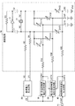
図1は、本発明の一実施形態に係る電圧制御発振器の構成例を示す図である。図1に示すように、この電圧制御発振器は、発振回路10と、基準電圧生成回路20と、第1の温度補償電圧生成回路30と、周波数制御電圧生成回路40と、第2の温度補償電圧生成回路50とを含んでも良い。あるいは、発振回路10〜第2の温度補償電圧生成回路50の一部が、半導体装置(IC)に内蔵されて、電圧制御発振器を構成しても良い。
<Voltage controlled oscillator>
FIG. 1 is a diagram illustrating a configuration example of a voltage controlled oscillator according to an embodiment of the present invention. As shown in FIG. 1, the voltage controlled oscillator includes an
発振回路10は、水晶振動体11と、インバーター12と、キャパシターC1〜C30と、抵抗R0〜R30と、第1群の可変容量素子CV11及びCV12と、第2群の可変容量素子CV21及びCV22と、第3群の可変容量素子CV31及びCV32とを含んでも良い。
The
あるいは、各群の可変容量素子において一方の可変容量素子を省略しても良い。その場合には、例えば、第1の可変容量素子CV11又はCV12と、第2の可変容量素子CV21又はCV22と、第3の可変容量素子CV31又はCV32とが、発振回路10に設けられることになる。
Alternatively, one of the variable capacitance elements in each group may be omitted. In that case, for example, the first variable capacitance element CV11 or CV12, the second variable capacitance element CV21 or CV22, and the third variable capacitance element CV31 or CV32 are provided in the
ここで、インバーター12、キャパシターC1及びC2、及び、抵抗R0は、水晶振動体11の第1の電極(ノードN1)と第2の電極(ノードN2)とに接続されて発振動作を行う発振部を構成する。キャパシターC1は、水晶振動体11の第1の電極(ノードN1)とインバーター12の入力端子との間に接続されている。キャパシターC2は、水晶振動体11の第2の電極(ノードN2)とインバーター12の出力端子との間に接続されている。抵抗R0は、インバーター12の出力端子と入力端子との間に接続されている。
Here, the
なお、インバーター12の替りに、例えば、バイポーラトランジスター1石で構成されるベース接地型の反転増幅回路を用いても良い。その場合には、キャパシターC1が、ノードN1とトランジスターのベースとの間に接続され、キャパシターC2が、ノードN2とトランジスターのコレクターとの間に接続され、抵抗R0が、トランジスターのコレクターとベースとの間に接続される。
Note that, instead of the
可変容量素子CV11、CV21、CV31の各々は、水晶振動体11の第1の電極(ノードN1)に接続された第1の端子を有し、発振回路10の発振周波数を調節する。また、可変容量素子CV12、CV22、CV32の各々は、水晶振動体11の第2の電極(ノードN2)に接続された第1の端子を有し、発振回路10の発振周波数を調節する。
Each of the variable capacitance elements CV11, CV21, and CV31 has a first terminal connected to a first electrode (node N1) of the
キャパシターC10は、第1群の可変容量素子CV11及びCV12の第2の端子と基準電圧VSSの配線との間に接続されている。キャパシターC20は、第2群の可変容量素子CV21及びCV22の第2の端子と基準電圧VSSの配線との間に接続されている。キャパシターC30は、第3群の可変容量素子CV31及びCV32の第2の端子と基準電位VSSの配線との間に接続されている。 The capacitor C10 is connected between the second terminals of the first group of variable capacitance elements CV11 and CV12 and the wiring of the reference voltage VSS. The capacitor C20 is connected between the second terminals of the second group of variable capacitance elements CV21 and CV22 and the wiring of the reference voltage VSS. The capacitor C30 is connected between the second terminals of the third group of variable capacitance elements CV31 and CV32 and the wiring of the reference potential VSS.
第1群の可変容量素子CV11及びCV12、第2群の可変容量素子CV21及びCV22、及び、第3群の可変容量素子CV31及びCV32の各々は、例えば、MOS構造を有するキャパシター、又は、可変容量ダイオード(バラクタダイオード)で構成され、第1の端子と第2の端子との間に印加される電圧に従って容量値が変化する。 Each of the first group of variable capacitance elements CV11 and CV12, the second group of variable capacitance elements CV21 and CV22, and the third group of variable capacitance elements CV31 and CV32 is, for example, a capacitor having a MOS structure or a variable capacitance. It is composed of a diode (varactor diode), and the capacitance value changes according to the voltage applied between the first terminal and the second terminal.
図2は、図1に示す可変容量素子の例としてMOS構造を有するキャパシターを示す図である。図2に示すキャパシターは、PチャネルMOSトランジスターで構成され、第1の端子13に接続されたゲート(G)と、基準電位VSSの配線に接続されたソース(S)及びドレイン(D)と、第2の端子14に接続されたバックゲート(Nウエル)とを有している。キャパシターの容量値は、MOSトランジスターのゲート長、ゲート幅、及び、ゲート絶縁膜の厚み等に依存する。
FIG. 2 is a diagram showing a capacitor having a MOS structure as an example of the variable capacitance element shown in FIG. The capacitor shown in FIG. 2 is composed of a P-channel MOS transistor, and has a gate (G) connected to the
キャパシターの第1の端子13と第2の端子14との間の電圧を上昇させてゆくと、バックゲートに形成される空乏層が次第に拡大して、キャパシターの容量値が次第に大きくなる。そして、電圧がある程度上昇すると、バックゲートに帯電する電荷の量が飽和して、キャパシターの容量値が飽和する。以下においては、一例として、キャパシターの第1の端子13が図1に示すノードN1又はN2に接続され、キャパシターの第2の端子14が図1に示す抵抗R10、R20、又は、R30に接続された場合について説明する。
As the voltage between the
再び図1を参照すると、インバーター12は反転増幅動作を行い、出力端子に生成される発振信号が、水晶振動体11等を介して入力端子にフィードバックされる。その際に、水晶振動体11は、インバーター12によって印加される交流電圧によって振動する。その振動は固有の共振周波数において大きく励起されて、水晶振動体11が負性抵抗として動作する。その結果、発振回路10は、主に水晶振動体11の共振周波数によって決定される発振周波数で発振する。ただし、可変容量素子CV11〜CV32の容量値を変更することによって、発振回路10の発振周波数を微調整することができる。
Referring to FIG. 1 again, the
基準電圧生成回路20は、例えば、バンドギャップリファレンス回路等を含み、電源電圧(VDD−VSS)が供給されて第1の基準電圧V1〜第3の基準電圧V3を生成する。第1の基準電圧V1は、抵抗R1を介してノードN1に供給され、第2の基準電圧V2は、抵抗R2を介してノードN2に供給される。第3の基準電圧V3は、第1の温度補償電圧生成回路30及び第2の温度補償電圧生成回路50に供給される。
The reference
第1の温度補償電圧生成回路30は、温度センサーから出力される検出信号に従って、第1群の可変容量素子CV11及びCV12の容量値を制御する第1の温度補償電圧VCOMPを生成する。第1の温度補償電圧VCOMPは、抵抗R10を介して第1群の可変容量素子CV11及びCV12の第2の端子に供給されると共に、第2の温度補償電圧生成回路50に供給される。
The first temperature compensation
図3は、図1に示す第1の温度補償電圧生成回路の構成例を示すブロック図である。図3に示すように、第1の温度補償電圧生成回路30は、温度センサー31と、ADコンバーター32と、1次電圧生成回路33と、3次電圧生成回路34と、加算回路35とを含んでも良い。
FIG. 3 is a block diagram showing a configuration example of the first temperature compensation voltage generation circuit shown in FIG. As shown in FIG. 3, the first temperature compensation
温度センサー31は、例えば、PN接合ダイオード、トランジスター、又は、サーミスターと、増幅回路とを含み、電圧制御発振器周辺の温度を検出して検出信号を出力する。ADコンバーター32は、温度センサー31から出力されるアナログの検出信号をデジタルの温度データに変換する。
The
1次電圧生成回路33及び3次電圧生成回路34は、例えば、水晶振動体11の共振周波数の温度依存性を相殺する温度特性を有する1次電圧及び3次電圧を表す電圧データを温度データに対応してそれぞれ格納する格納部と、DAコンバーターとを有している。1次電圧生成回路33及び3次電圧生成回路34は、ADコンバーター32から出力される温度データに対応する電圧データを格納部から読み出し、電圧データを1次電圧及び3次電圧にそれぞれ変換して出力する。
The primary
加算回路35は、1次電圧生成回路33から出力される1次電圧と3次電圧生成回路34から出力される3次電圧とを加算して、第1の温度補償電圧VCOMPを生成する。第1の温度補償電圧VCOMPは、発振回路10が基準温度(例えば、25℃)において基準周波数f0で発振する場合に、第3の基準電圧V3と略等しくなるように設定される。
The
第1の温度補償電圧VCOMPが第3の基準電圧V3よりも低くなると、第1群の可変容量素子CV11及びCV12の容量値が増大して発振周波数が低下する。一方、第1の温度補償電圧VCOMPが第3の基準電圧V3よりも高くなると、第1群の可変容量素子CV11及びCV12の容量値が低下して発振周波数が上昇する。 When the first temperature compensation voltage VCOMP becomes lower than the third reference voltage V3, the capacitance values of the first group of variable capacitance elements CV11 and CV12 increase, and the oscillation frequency decreases. On the other hand, when the first temperature compensation voltage VCOMP becomes higher than the third reference voltage V3, the capacitance values of the first group of variable capacitance elements CV11 and CV12 decrease, and the oscillation frequency increases.
あるいは、ADコンバーター32を用いずに、アナログ回路のみで第1の温度補償電圧生成回路30を構成しても良い。その場合に、1次電圧生成回路33及び3次電圧生成回路34は、温度センサー31から出力されるアナログの検出信号に基づいて、水晶振動体11の共振周波数の温度依存性を相殺する温度特性を有する1次電圧及び3次電圧をそれぞれ生成する。
Alternatively, the first temperature compensation
再び図1を参照すると、周波数制御電圧生成回路40は、例えば、増幅回路等を含み、入力端子41に印加される周波数制御信号CONTに従って、第2群の可変容量素子CV21及びCV22の容量値を制御する周波数制御電圧VAFCを生成する。周波数制御信号CONTは、アナログ信号(制御電圧)でも良いし、デジタル信号でも良い。
Referring to FIG. 1 again, the frequency control
デジタル信号をシリアル伝送する場合には、例えば、SPI規格又はI2C規格等を用いることができる。周波数制御電圧生成回路40は、シリアル伝送を行うためのシリアルクロック信号と、発振周波数を制御するためのシリアルの制御データと、半導体装置(チップ)を選択するためのチップセレクト信号とを受信して、制御データを周波数制御電圧VAFCに変換しても良い。
When digital signals are transmitted serially, for example, the SPI standard or the I2C standard can be used. The frequency control
周波数制御電圧VAFCは、抵抗R20を介して第2群の可変容量素子CV21及びCV22の第2の端子に供給される。それにより、図1に示す電圧制御発振器を備えた電子機器等は、周波数制御信号CONTを用いて、発振回路10の発振周波数を必要に応じて偏移させたり変調したりすることができる。
The frequency control voltage VAFC is supplied to the second terminals of the second group of variable capacitance elements CV21 and CV22 via the resistor R20. Thereby, an electronic device or the like including the voltage-controlled oscillator shown in FIG. 1 can shift or modulate the oscillation frequency of the
発振回路10を基準周波数f0で発振させる場合に、周波数制御電圧VAFCが所定の値に設定される。そのとき、第2群の可変容量素子CV21及びCV22の容量値は基準容量値になる。また、発振回路10を基準周波数f0よりも低い周波数で発振させる場合には、周波数制御電圧VAFCが所定の値よりも低く設定される。そのとき、第2群の可変容量素子CV21及びCV22の容量値は基準容量値よりも大きくなる。一方、発振回路10を基準周波数f0よりも高い周波数で発振させる場合には、周波数制御電圧VAFCが所定の値よりも高く設定される。そのとき、第2群の可変容量素子CV21及びCV22の容量値は基準容量値よりも小さくなる。
When oscillating the
第1の温度補償電圧生成回路30の格納部に格納されている電圧データは、周波数制御電圧VAFCが所定の値である場合に、発振回路10が所定の温度範囲において基準周波数f0と略等しい周波数で発振するように設定されている。しかしながら、周波数制御電圧VAFCが所定の値よりも低くなって第2群の可変容量素子CV21及びCV22の容量値が基準容量値よりも大きくなると、温度補償が不足する。一方、周波数制御電圧VAFCが所定の値よりも高くなって第2群の可変容量素子CV21及びCV22の容量値が基準容量値よりも小さくなると、温度補償が過剰になる。そこで、これを補正するために、第2の温度補償電圧生成回路50が設けられている。
The voltage data stored in the storage unit of the first temperature compensation
第2の温度補償電圧生成回路50は、周波数制御電圧VAFCの変化によって生じる温度補償量の変化を補正するために、第1の温度補償電圧VCOMP及び周波数制御電圧VAFCに基づいて、第3群の可変容量素子CV31及びCV32の容量値を制御する第2の温度補償電圧VATRを生成する。第2の温度補償電圧VATRは、抵抗R30を介して第3群の可変容量素子CV31及びCV32の第2の端子に供給される。
The second temperature compensation
図4は、図1に示す第2の温度補償電圧生成回路の構成例を示す回路図である。図4に示すように、第2の温度補償電圧生成回路50は、増幅回路としてのオペアンプ51〜53と、抵抗R51〜R57と、NチャネルMOSトランジスターQN1とを含んでいる。オペアンプ51〜53は、第3の基準電圧V3を基準として増幅動作を行う。
FIG. 4 is a circuit diagram showing a configuration example of the second temperature compensation voltage generation circuit shown in FIG. As shown in FIG. 4, the second temperature compensation
オペアンプ51は、抵抗R51を介して反転入力端子に入力される周波数制御電圧VAFCを反転増幅する。オペアンプ51の反転入力端子と電源電位VDDの配線との間には、オペアンプ51の出力信号のDCレベルを調節するための抵抗R52が接続されている。また、オペアンプ51の出力端子と反転入力端子との間には、抵抗R53が接続されている。オペアンプ51の電圧増幅率は、抵抗R51及びR53によって設定される。
The
図4に示すように、抵抗R52及びR53の抵抗値を可変にしても良い。例えば、第2の温度補償電圧生成回路50は、抵抗R52及びR53の抵抗値を設定するための設定データを格納する格納部を有しており、設定データに従って抵抗R52及びR53の抵抗値を設定する。
As shown in FIG. 4, the resistance values of the resistors R52 and R53 may be variable. For example, the second temperature compensation
オペアンプ52は、抵抗R54を介して反転入力端子に入力されるオペアンプ51の出力信号を反転増幅し、増幅された信号を増幅率補正信号として出力する。オペアンプ52の出力端子と反転入力端子との間には、抵抗R55が接続されている。オペアンプ52の電圧増幅率は、抵抗R54及びR55によって設定される。
The
オペアンプ53は、非反転入力端子に入力される第1の温度補償電圧VCOMPを増幅し、増幅された電圧を第2の温度補償電圧VATRとして出力する。オペアンプ53の反転入力端子と第3の基準電圧V3の配線との間には、抵抗R56が接続されている。また、オペアンプ53の出力端子と反転入力端子との間には、抵抗R57及びトランジスターQN1が並列に接続されている。オペアンプ53の電圧増幅率は、抵抗R56及びR57と、トランジスターQN1とによって設定される。
The
トランジスターQN1は、オペアンプ53の反転入力端子に接続されたドレイン(D)と、オペアンプ53の出力端子に接続されたソース(S)と、オペアンプ52から出力される増幅率補正信号が印加されるゲート(G)とを有している。トランジスターQN1のオン抵抗は、ゲート電圧によって変化する。
The transistor QN1 has a drain (D) connected to the inverting input terminal of the
即ち、増幅率補正信号の電圧を上昇させると、トランジスターQN1のオン抵抗が低下して、オペアンプ53の電圧増幅率が低下する。一方、増幅率補正信号の電圧を低下させると、トランジスターQN1のオン抵抗が上昇して、オペアンプ53の電圧増幅率が上昇する。
That is, when the voltage of the amplification factor correction signal is increased, the on-resistance of the transistor QN1 decreases, and the voltage amplification factor of the
従って、トランジスターQN1は、増幅率補正信号に従って第2の温度補償電圧生成回路50の電圧増幅率αを調整する増幅率調整回路を構成している。第2の温度補償電圧生成回路50の電圧増幅率αは、第1の温度補償電圧VCOMPの第3の基準電圧V3に対する差分D1と、第2の温度補償電圧VATRの第3の基準電圧V3に対する差分D2とによって表される(α=D2/D1)。
Therefore, the transistor QN1 forms an amplification factor adjustment circuit that adjusts the voltage amplification factor α of the second temperature compensation
オペアンプ52から出力される増幅率補正信号の電圧は、周波数制御電圧VAFCの上昇に伴って上昇する。従って、周波数制御電圧VAFCの上昇に伴って第2の温度補償電圧生成回路50の電圧増幅率αが低下する。ここで、周波数制御電圧VAFCが所定の値であるときに第2の温度補償電圧生成回路50の電圧増幅率αが基準増幅率α0となるように、抵抗R51〜R57の抵抗値が設定される。
The voltage of the amplification factor correction signal output from the
このように、第2の温度補償電圧生成回路50は、周波数制御電圧VAFCに応じた電圧増幅率αで第1の温度補償電圧VCOMPを増幅することにより、第2の温度補償電圧VATRを生成する。それにより、周波数制御電圧VAFCの変化によって生じる第1群の可変容量素子CV11及びCV12の感度(電圧変化に対する容量変化率の割合)の変化を補正するように、第3群の可変容量素子CV31及びCV32の容量値を変化させることができる。
As described above, the second temperature compensation
第2の温度補償電圧VATRが第3の基準電圧V3よりも低くなると、第3群の可変容量素子CV31及びCV32の容量値が増大して発振周波数が低下する。一方、第2の温度補償電圧VATRが第3の基準電圧V3よりも高くなると、第3群の可変容量素子CV31及びCV32の容量値が低下して発振周波数が上昇する。 When the second temperature compensation voltage VATR becomes lower than the third reference voltage V3, the capacitance values of the third group of variable capacitance elements CV31 and CV32 increase, and the oscillation frequency decreases. On the other hand, when the second temperature compensation voltage VATR becomes higher than the third reference voltage V3, the capacitance values of the third group of variable capacitance elements CV31 and CV32 decrease, and the oscillation frequency increases.
図5は、図1に示す電圧制御発振器における温度補償動作の例を説明するための模式図である。図5において、横軸は温度を表しており、縦軸は周波数を表している。また、図5(a)は、周波数制御電圧VAFCが所定の値である場合を示し、図5(b)は、周波数制御電圧VAFCが所定の値よりも低い場合を示し、図5(c)は、周波数制御電圧VAFCが所定の値よりも高い場合を示している。ただし、水晶振動体11の共振周波数は、基準温度における共振周波数が縦軸の周波数f0〜f2に一致するように移動したものである。
FIG. 5 is a schematic diagram for explaining an example of a temperature compensation operation in the voltage controlled oscillator shown in FIG. In FIG. 5, the horizontal axis represents temperature, and the vertical axis represents frequency. FIG. 5A shows a case where the frequency control voltage VAFC has a predetermined value, FIG. 5B shows a case where the frequency control voltage VAFC is lower than the predetermined value, and FIG. Shows a case where the frequency control voltage VAFC is higher than a predetermined value. However, the resonance frequency of the
図5(a)を参照すると、周波数制御電圧VAFCが所定の値である場合には、第2群の可変容量素子CV21及びCV22の容量値が基準容量値になる。従って、第1群の可変容量素子CV11及びCV12の感度が基準感度になると共に、第3群の可変容量素子CV31及びCV32の感度が基準感度になる。 Referring to FIG. 5A, when the frequency control voltage VAFC has a predetermined value, the capacitance value of the second group of variable capacitance elements CV21 and CV22 becomes the reference capacitance value. Accordingly, the sensitivity of the first group of variable capacitance elements CV11 and CV12 becomes the reference sensitivity, and the sensitivity of the third group of variable capacitance elements CV31 and CV32 becomes the reference sensitivity.
その際に、第2の温度補償電圧生成回路50は、第1の温度補償電圧VCOMPを基準増幅率α0で増幅して得られた第2の温度補償電圧VATRを第3群の可変容量素子CV31及びCV32の第2の端子に印加する。この例においては、第2の温度補償電圧生成回路50の基準増幅率α0と第3群の可変容量素子CV31及びCV32の感度との積が、第1群の可変容量素子CV11及びCV12の感度と略等しく設定されている。
At that time, the second temperature compensation
それにより、第3群の可変容量素子CV31及びCV32による温度補償量が、第1群の可変容量素子CV11及びCV12による温度補償量と略等しくなる。その結果、水晶振動体11の共振周波数の温度補償が適切に行われて、発振回路10の発振周波数が所定の温度範囲において基準周波数f0に調整される。
As a result, the amount of temperature compensation by the third group of variable capacitance elements CV31 and CV32 becomes substantially equal to the amount of temperature compensation by the first group of variable capacitance elements CV11 and CV12. Consequently, the temperature compensation of the resonance frequency of the
図5(b)を参照すると、周波数制御電圧VAFCが所定の値よりも低い場合には、第2群の可変容量素子CV21及びCV22の容量値が基準容量値よりも大きくなる。従って、第1群の可変容量素子CV11及びCV12の感度が基準感度よりも低くなると共に、第3群の可変容量素子CV31及びCV32の感度が基準感度よりも低くなって、温度補償量が不足する。 Referring to FIG. 5B, when the frequency control voltage VAFC is lower than a predetermined value, the capacitance values of the second group of variable capacitance elements CV21 and CV22 become larger than the reference capacitance value. Therefore, the sensitivities of the first group of variable capacitance elements CV11 and CV12 are lower than the reference sensitivity, and the sensitivities of the third group of variable capacitance elements CV31 and CV32 are lower than the reference sensitivity. .
その際に、第2の温度補償電圧生成回路50は、第1の温度補償電圧VCOMPを基準増幅率α0よりも大きい電圧増幅率で増幅して得られた第2の温度補償電圧VATRを第3群の可変容量素子CV31及びCV32の第2の端子に印加する。それにより、第3群の可変容量素子CV31及びCV32による温度補償量は、第1群の可変容量素子CV11及びCV12による温度補償量よりも大きくなる。その結果、第1群の可変容量素子CV11及びCV12による温度補償量の不足が補正されて、発振回路10の発振周波数が所定の温度範囲において周波数f1(<f0)に調整される。
At that time, the second temperature compensation
図5(c)を参照すると、周波数制御電圧VAFCが所定の値よりも高い場合には、第2群の可変容量素子CV21及びCV22の容量値が基準容量値よりも小さくなる。従って、第1群の可変容量素子CV11及びCV12の感度が基準感度よりも高くなると共に、第3群の可変容量素子CV31及びCV32の感度が基準感度よりも高くなって、温度補償量が過剰になる。 Referring to FIG. 5C, when the frequency control voltage VAFC is higher than a predetermined value, the capacitance values of the second group of variable capacitance elements CV21 and CV22 are smaller than the reference capacitance value. Accordingly, the sensitivities of the first group of variable capacitance elements CV11 and CV12 are higher than the reference sensitivity, and the sensitivities of the third group of variable capacitance elements CV31 and CV32 are higher than the reference sensitivity. Become.
その際に、第2の温度補償電圧生成回路50は、第1の温度補償電圧VCOMPを基準増幅率α0よりも小さい電圧増幅率で増幅して得られた第2の温度補償電圧VATRを第3群の可変容量素子CV31及びCV32の第2の端子に印加する。それにより、第3群の可変容量素子CV31及びCV32による温度補償量は、第1群の可変容量素子CV11及びCV12による温度補償量よりも小さくなる。その結果、第1群の可変容量素子CV11及びCV12による温度補償量の過剰が補正されて、発振回路10の発振周波数が所定の温度範囲において周波数f2(>f0)に調整される。
At that time, the second temperature compensation
図6は、図1に示す可変容量素子に印加される制御電圧(温度補償電圧)の範囲を従来技術と比較しながら説明するための図である。図6において、横軸は、可変容量素子に対する印加電圧(V)を表しており、縦軸は、可変容量素子の感度(ppm/V)を表している。 FIG. 6 is a diagram for explaining a range of a control voltage (temperature compensation voltage) applied to the variable capacitance element shown in FIG. 1 while comparing with a conventional technique. 6, the horizontal axis represents the applied voltage (V) to the variable capacitance element, and the vertical axis represents the sensitivity (ppm / V) of the variable capacitance element.
図6(a)は、特許文献1に開示されている温度補償型発振回路10の第1可変容量素子16に印加される制御電圧に対する第1可変容量素子16の感度を示している。第1可変容量素子16は、所定の電圧範囲において最大の感度(例えば、約50ppm/V)を有しており、制御電圧が所定の電圧範囲から外れると、感度が低下してリニアリティが悪化する。
FIG. 6A shows the sensitivity of the first variable capacitance element 16 to the control voltage applied to the first variable capacitance element 16 of the temperature compensated
特許文献1においては、第1可変容量素子16の第1の端子に温度補償電圧が印加されると共に、同一の第1可変容量素子16の第2の端子に補助温度補償電圧が印加されるので、温度補償電圧と補助温度補償電圧との差である制御電圧が所定の電圧範囲から外れ易くなる。 In Patent Document 1, the temperature compensation voltage is applied to the first terminal of the first variable capacitance element 16 and the auxiliary temperature compensation voltage is applied to the second terminal of the same first variable capacitance element 16. In addition, the control voltage, which is the difference between the temperature compensation voltage and the auxiliary temperature compensation voltage, tends to be out of the predetermined voltage range.
従って、感度のリニアリティが良好な状態で使用することが可能な制御電圧の範囲が制限されてしまう。また、第1可変容量素子16は、温度補償のために高い感度を有しているので、制御電圧に含まれているノイズ成分によって発振信号の位相ノイズが増加するおそれがある。 Therefore, the range of the control voltage that can be used with good sensitivity linearity is limited. In addition, since the first variable capacitance element 16 has high sensitivity for temperature compensation, the phase noise of the oscillation signal may increase due to a noise component included in the control voltage.
図6(b)は、本願の図1に示す第1群の可変容量素子CV11及びCV12に印加される制御電圧に対する第1群の可変容量素子CV11及びCV12の感度を示している。第1群の可変容量素子CV11及びCV12は、所定の電圧範囲において最大の感度(例えば、約50ppm/V)を有しており、制御電圧が所定の電圧範囲から外れると、感度が低下してリニアリティが悪化する。ただし、第1群の可変容量素子CV11及びCV12には、第1の温度補償電圧VCOMPのみが印加されるので、制御電圧が所定の電圧範囲から外れ難くなる。 FIG. 6B shows the sensitivity of the first group of variable capacitance elements CV11 and CV12 to the control voltage applied to the first group of variable capacitance elements CV11 and CV12 shown in FIG. 1 of the present application. The first group of variable capacitance elements CV11 and CV12 have the maximum sensitivity (for example, about 50 ppm / V) in a predetermined voltage range, and the sensitivity decreases when the control voltage deviates from the predetermined voltage range. Linearity deteriorates. However, since only the first temperature compensation voltage VCOMP is applied to the first group of variable capacitance elements CV11 and CV12, it is difficult for the control voltage to deviate from the predetermined voltage range.
図6(c)は、本願の図1に示す第3群の可変容量素子CV31及びCV32に印加される制御電圧に対する第3群の可変容量素子CV31及びCV32の感度を示している。第3群の可変容量素子CV31及びCV32は、所定の電圧範囲において最大の感度(例えば、約25ppm/V)を有しており、制御電圧が所定の電圧範囲から外れると、感度が低下してリニアリティが悪化する。ただし、第3群の可変容量素子CV31及びCV32には、第2の温度補償電圧VATRのみが印加されるので、制御電圧が所定の電圧範囲から外れ難くなる。 FIG. 6C shows the sensitivity of the third group of variable capacitance elements CV31 and CV32 to the control voltage applied to the third group of variable capacitance elements CV31 and CV32 shown in FIG. 1 of the present application. The variable capacitance elements CV31 and CV32 of the third group have the maximum sensitivity (for example, about 25 ppm / V) in a predetermined voltage range, and the sensitivity decreases when the control voltage deviates from the predetermined voltage range. Linearity deteriorates. However, since only the second temperature compensation voltage VATR is applied to the third group of variable capacitance elements CV31 and CV32, the control voltage does not easily fall out of the predetermined voltage range.
このように、本実施形態によれば、第1の温度補償電圧VCOMPに従って発振周波数を調節する第1群の可変容量素子CV11及びCV12、及び、周波数制御電圧VAFCに従って発振周波数を調節する第2群の可変容量素子CV21及びCV22とは別個に、第2の温度補償電圧VATRに従って発振周波数を調節する第3群の可変容量素子CV31及びCV32が設けられている。 As described above, according to the present embodiment, the first group of variable capacitance elements CV11 and CV12 for adjusting the oscillation frequency according to the first temperature compensation voltage VCOMP, and the second group for adjusting the oscillation frequency according to the frequency control voltage VAFC. A third group of variable capacitance elements CV31 and CV32 for adjusting the oscillation frequency according to the second temperature compensation voltage VATR is provided separately from the variable capacitance elements CV21 and CV22.
また、第2の温度補償電圧生成回路50が、第1の温度補償電圧VCOMP及び周波数制御電圧VAFCに基づいて第2の温度補償電圧VATRを生成する。それにより、第1群の可変容量素子CV11及びCV12を感度のリニアリティが良好な状態で使用することが可能な制御電圧の範囲を拡大することができる。
Further, the second temperature compensation
ここで、第2の温度補償電圧VATRが、第1群の可変容量素子CV11及びCV12、及び、第2群の可変容量素子CV21及びCV22に印加されないことが望ましい。その場合には、第2の温度補償電圧VATRが第3群の可変容量素子CV31及びCV32のみに印加されるので、第1群の可変容量素子CV11及びCV12、及び、第2群の可変容量素子CV21及びCV22を感度のリニアリティが良好な状態で使用することができる。 Here, it is desirable that the second temperature compensation voltage VATR is not applied to the first group of variable capacitance elements CV11 and CV12 and the second group of variable capacitance elements CV21 and CV22. In this case, since the second temperature compensation voltage VATR is applied only to the third group of variable capacitance elements CV31 and CV32, the first group of variable capacitance elements CV11 and CV12 and the second group of variable capacitance elements CV21 and CV22 can be used with good sensitivity linearity.
また、第3群の可変容量素子CV31及びCV32の感度が、第1群の可変容量素子CV11及びCV12の感度よりも低く、且つ、第2群の可変容量素子CV21及びCV22の感度よりも低くても良い。 Also, the sensitivity of the third group of variable capacitance elements CV31 and CV32 is lower than the sensitivity of the first group of variable capacitance elements CV11 and CV12, and lower than the sensitivity of the second group of variable capacitance elements CV21 and CV22. Is also good.
その場合には、第2の温度補償電圧VATRにノイズ成分が含まれていたとしても、それに起因する発振信号の位相ノイズを低減することができる。例えば、第2の温度補償電圧VATRに残留ノイズやコモンモードノイズ等が含まれていたとしても、第3群の可変容量素子CV31及びCV32の感度が低ければ、発振信号の位相に与える影響が低減される。 In this case, even if the second temperature compensation voltage VATR includes a noise component, the phase noise of the oscillation signal caused by the noise component can be reduced. For example, even if the second temperature compensation voltage VATR contains residual noise, common mode noise, and the like, if the sensitivity of the third group of variable capacitance elements CV31 and CV32 is low, the influence on the phase of the oscillation signal is reduced. Is done.
さらに、第3群の可変容量素子CV31及びCV32の感度のリニアリティ幅が、第1群の可変容量素子CV11及びCV12の感度のリニアリティ幅よりも広く、且つ、第2群の可変容量素子CV21及びCV22の感度のリニアリティ幅よりも広くても良い。その場合には、第3群の可変容量素子CV31及びCV32を感度のリニアリティが良好な状態で使用することができる。なお、本願において、感度のリニアリティ幅とは、可変容量素子の感度が最大感度の所定の割合以上(例えば、80%以上)となるような印加電圧の幅のことをいう。 Further, the sensitivity linearity width of the third group of variable capacitance elements CV31 and CV32 is wider than the sensitivity linearity width of the first group of variable capacitance elements CV11 and CV12, and the second group of variable capacitance elements CV21 and CV22. May be wider than the sensitivity linearity range. In this case, the variable capacitance elements CV31 and CV32 of the third group can be used in a state where the linearity of sensitivity is good. In the present application, the sensitivity linearity width refers to a width of an applied voltage at which the sensitivity of the variable capacitance element is equal to or more than a predetermined ratio of the maximum sensitivity (for example, 80% or more).
<電子機器>
次に、本発明の一実施形態に係る電圧制御発振器を用いた電子機器について説明する。
図7は、本発明の一実施形態に係る電子機器の第1の構成例を示すブロック図である。この電子機器は、本発明の一実施形態に係る電圧制御発振器110と、CPU120と、操作部130と、ROM(リードオンリー・メモリー)140と、RAM(ランダムアクセス・メモリー)150と、通信部160と、表示部170と、音声出力部180とを含んでいる。なお、図7に示す構成要素の一部を省略又は変更しても良いし、あるいは、図7に示す構成要素に他の構成要素を付加しても良い。
<Electronic equipment>
Next, an electronic device using the voltage controlled oscillator according to one embodiment of the present invention will be described.
FIG. 7 is a block diagram illustrating a first configuration example of an electronic device according to an embodiment of the present invention. The electronic device includes a voltage controlled
電圧制御発振器110は、周波数制御信号によって制御される発振周波数で発振動作を行うことにより、クロック信号を生成する。電圧制御発振器110によって生成されるクロック信号は、CPU120等を介して、電子機器の各部に供給される。
The voltage controlled
CPU120は、電圧制御発振器110から供給されるクロック信号に同期して動作し、ROM140等に記憶されているプログラムに従って、各種の信号処理や制御処理を行う。例えば、CPU120は、操作部130から供給される操作信号に応じて各種の信号処理を行ったり、外部との間でデータ通信を行うために通信部160を制御する。あるいは、CPU120は、表示部170に各種の画像を表示させるための画像信号を生成したり、音声出力部180に各種の音声を出力させるための音声信号を生成する。
The
操作部130は、例えば、操作キーやボタンスイッチ等を含む入力装置であり、ユーザーによる操作に応じた操作信号をCPU120に出力する。ROM140は、CPU120が各種の信号処理や制御処理を行うためのプログラムやデータ等を記憶している。また、RAM150は、CPU120の作業領域として用いられ、ROM140から読み出されたプログラムやデータ、操作部130を用いて入力されたデータ、又は、CPU120がプログラムに従って実行した演算結果等を一時的に記憶する。
The
通信部160は、例えば、アナログ回路及びデジタル回路で構成され、CPU120と外部装置との間のデータ通信を行う。表示部170は、例えば、LCD(液晶表示装置)等を含み、CPU120から供給される画像信号に基づいて各種の情報を表示する。また、音声出力部180は、例えば、スピーカー等を含み、CPU120から供給される音声信号に基づいて音声を出力する。
The
上記の電子機器としては、例えば、携帯電話機等の移動端末、スマートカード、電卓、電子辞書、電子ゲーム機器、デジタルスチルカメラ、デジタルムービー、テレビ、テレビ電話、防犯用テレビモニター、ヘッドマウント・ディスプレイ、パーソナルコンピューター、プリンター、ネットワーク機器、カーナビゲーション装置、測定機器、及び、医療機器(例えば、電子体温計、血圧計、血糖計、心電図計測装置、超音波診断装置、及び、電子内視鏡)等が該当する。 Examples of the electronic device include a mobile terminal such as a mobile phone, a smart card, a calculator, an electronic dictionary, an electronic game device, a digital still camera, a digital movie, a television, a videophone, a security television monitor, a head mounted display, Personal computers, printers, network devices, car navigation devices, measuring devices, and medical devices (eg, electronic thermometers, sphygmomanometers, blood glucose meters, electrocardiogram measuring devices, ultrasonic diagnostic devices, and electronic endoscopes) I do.
図8は、本発明の一実施形態に係る電子機器の第2の構成例を示すブロック図である。この例においては、時計及びタイマーについて説明する。本発明の一実施形態に係る時計は、本発明の一実施形態に係る電圧制御発振器110と、分周器111と、操作部130と、表示部170と、音声出力部180と、計時部190とを含んでいる。また、本発明の一実施形態に係るタイマーは、音声出力部180の替りに制御部200を含んでいる。なお、図8に示す構成要素の一部を省略又は変更しても良いし、あるいは、図8に示す構成要素に他の構成要素を付加しても良い。
FIG. 8 is a block diagram illustrating a second configuration example of the electronic device according to the embodiment of the present invention. In this example, a clock and a timer will be described. The timepiece according to one embodiment of the present invention includes a voltage controlled
分周器111は、例えば、複数のフリップフロップ等で構成され、電圧制御発振器110から供給されるクロック信号を分周して、計時用の分周クロック信号を生成する。計時部190は、例えば、カウンター等で構成され、分周器111から供給される分周クロック信号に基づいて計時動作を行って、現在時刻やアラーム時刻を表す表示信号や、アラーム音を発生するためのアラーム信号を生成する。
The
操作部130は、計時部190に現在時刻やアラーム時刻を設定するために用いられる。表示部170は、計時部190から供給される表示信号に従って、現在時刻やアラーム時刻を表示する。音声出力部180は、計時部190から供給されるアラーム信号に従って、アラーム音を発生する。
The
タイマーの場合には、アラーム機能の替りにタイマー機能が設けられる。即ち、計時部190は、現在時刻が設定時刻に一致したことを表すタイマー信号を生成する。制御部200は、計時部190から供給されるタイマー信号に従って、タイマーに接続されている機器をオン又はオフさせる。
In the case of a timer, a timer function is provided instead of the alarm function. That is, the
本実施形態によれば、周波数制御信号を用いて発振周波数を調節する際の温度補償特性が改善された電圧制御発振器110によって生成される正確なクロック信号で動作する電子機器を提供することができる。
According to the present embodiment, it is possible to provide an electronic device that operates with an accurate clock signal generated by the voltage controlled
<移動体>
次に、本発明の一実施形態に係る電圧制御発振器を用いた移動体について説明する。移動体としては、例えば、自動車、自走式ロボット、自走式搬送機器、列車、船舶、飛行機、又は、人工衛星等が該当する。
<Mobile>
Next, a moving object using the voltage controlled oscillator according to one embodiment of the present invention will be described. Examples of the moving object include an automobile, a self-propelled robot, a self-propelled transport device, a train, a ship, an airplane, and an artificial satellite.
図9は、本発明の一実施形態に係る移動体の構成例を示すブロック図である。図9に示すように、この移動体は、本発明の一実施形態に係る電圧制御発振器110を含み、さらに、電子制御式燃料噴射装置210、電子制御式ABS装置220、又は、電子制御式一定速度走行装置230等の各種の電子制御式装置を搭載している。なお、図9に示す構成要素の一部を省略又は変更しても良いし、あるいは、図9に示す構成要素に他の構成要素を付加しても良い。
FIG. 9 is a block diagram illustrating a configuration example of a moving object according to an embodiment of the present invention. As shown in FIG. 9, the moving object includes a voltage controlled
電圧制御発振器110は、周波数制御信号によって制御される発振周波数で発振動作を行うことにより、クロック信号を生成する。電圧制御発振器110によって生成されるクロック信号は、電子制御式燃料噴射装置210、電子制御式ABS装置220、又は、電子制御式一定速度走行装置230等に供給される。
The
電子制御式燃料噴射装置210は、電圧制御発振器110から供給されるクロック信号に同期して動作し、ガソリンエンジン等の予混合燃焼機関において、所定のタイミングで液体の燃料を吸入空気に霧状に噴射する。電子制御式ABS(アンチロック・ブレーキ・システム)装置220は、電圧制御発振器110から供給されるクロック信号に同期して動作し、ブレーキをかけるように操作が行われた際に、ブレーキを徐々に強力に駆動して、移動体が滑り始めたらブレーキを一旦緩めてから再び駆動することを繰り返す。電子制御式一定速度走行装置230は、電圧制御発振器110から供給されるクロック信号に同期して動作し、移動体の速度を監視しながら、移動体の速度が一定となるようにアクセル又はブレーキ等を制御する。
The electronically controlled
本実施形態によれば、周波数制御信号を用いて発振周波数を調節する際の温度補償特性が改善された電圧制御発振器110によって生成される正確なクロック信号で動作する移動体を提供することができる。
According to the present embodiment, it is possible to provide a moving object that operates with an accurate clock signal generated by the voltage controlled
上記の実施形態においては、水晶振動体を用いた電圧制御発振器について説明したが、本発明は、以上説明した実施形態に限定されるものではなく、水晶以外の圧電体等を用いた発振器にも適用することができる。このように、当該技術分野において通常の知識を有する者によって、本発明の技術的思想内で多くの変形が可能である。 In the above embodiment, the voltage controlled oscillator using the crystal vibrator has been described.However, the present invention is not limited to the embodiment described above, and may be applied to an oscillator using a piezoelectric body or the like other than crystal. Can be applied. Thus, many modifications can be made by a person having ordinary skill in the art within the spirit of the invention.
10…発振回路、11…水晶振動体、12…インバーター、20…基準電圧生成回路、30…第1の温度補償電圧生成回路、31…温度センサー、32…ADコンバーター、33…1次電圧生成回路、34…3次電圧生成回路、35…加算回路、40…周波数制御電圧生成回路、41…入力端子、50…第2の温度補償電圧生成回路、51〜53…オペアンプ、110…電圧制御発振器、111…分周器、120…CPU、130…操作部、140…ROM、150…RAM、160…通信部、170…表示部、180…音声出力部、190…計時部、200…制御部、210…電子制御式燃料噴射装置、220…電子制御式ABS装置、230…電子制御式一定速度走行装置、C1〜C30…キャパシター、R0〜R57…抵抗、CV11〜CV32…可変容量素子、QN1…NチャネルMOSトランジスター
DESCRIPTION OF
Claims (7)
前記振動体の第1又は第2の電極に接続されて発振周波数を調節する第1〜第3の可変容量素子と、
温度センサーから出力される検出信号に従って、前記第1の可変容量素子の容量値を制御する第1の温度補償電圧を生成する第1の温度補償電圧生成回路と、
周波数制御信号に従って、前記第2の可変容量素子の容量値を制御する周波数制御電圧を生成する周波数制御電圧生成回路と、
前記第1の温度補償電圧及び前記周波数制御電圧に基づいて、前記第3の可変容量素子の容量値を制御する第2の温度補償電圧を生成し、前記周波数制御電圧の変化によって生じる温度補償量の変化を低減する第2の温度補償電圧生成回路と、を備える電圧制御発振器。 An oscillating unit connected to the first electrode and the second electrode of the vibrator to perform an oscillating operation;
First to third variable capacitance elements connected to the first or second electrode of the vibrator to adjust the oscillation frequency;
A first temperature compensation voltage generation circuit that generates a first temperature compensation voltage that controls a capacitance value of the first variable capacitance element according to a detection signal output from the temperature sensor;
A frequency control voltage generation circuit that generates a frequency control voltage that controls a capacitance value of the second variable capacitance element according to a frequency control signal;
A second temperature compensation voltage for controlling a capacitance value of the third variable capacitance element is generated based on the first temperature compensation voltage and the frequency control voltage, and a temperature compensation amount generated by a change in the frequency control voltage And a second temperature-compensated voltage generation circuit that reduces the change in the voltage.
Priority Applications (1)
| Application Number | Priority Date | Filing Date | Title |
|---|---|---|---|
| JP2015247052A JP6651834B2 (en) | 2015-12-18 | 2015-12-18 | Voltage-controlled oscillator, electronic device, and moving object |
Applications Claiming Priority (1)
| Application Number | Priority Date | Filing Date | Title |
|---|---|---|---|
| JP2015247052A JP6651834B2 (en) | 2015-12-18 | 2015-12-18 | Voltage-controlled oscillator, electronic device, and moving object |
Publications (3)
| Publication Number | Publication Date |
|---|---|
| JP2017112557A JP2017112557A (en) | 2017-06-22 |
| JP2017112557A5 JP2017112557A5 (en) | 2018-12-20 |
| JP6651834B2 true JP6651834B2 (en) | 2020-02-19 |
Family
ID=59079839
Family Applications (1)
| Application Number | Title | Priority Date | Filing Date |
|---|---|---|---|
| JP2015247052A Active JP6651834B2 (en) | 2015-12-18 | 2015-12-18 | Voltage-controlled oscillator, electronic device, and moving object |
Country Status (1)
| Country | Link |
|---|---|
| JP (1) | JP6651834B2 (en) |
Families Citing this family (1)
| Publication number | Priority date | Publication date | Assignee | Title |
|---|---|---|---|---|
| JP2023073611A (en) | 2021-11-16 | 2023-05-26 | セイコーエプソン株式会社 | Circuit device and oscillator |
Family Cites Families (4)
| Publication number | Priority date | Publication date | Assignee | Title |
|---|---|---|---|---|
| JP2010130141A (en) * | 2008-11-26 | 2010-06-10 | Epson Toyocom Corp | Voltage controlled temperature compensation piezoelectric oscillator |
| JP5299628B2 (en) * | 2009-03-18 | 2013-09-25 | セイコーエプソン株式会社 | Temperature compensated voltage generation circuit, temperature compensated oscillation circuit |
| JP2015104074A (en) * | 2013-11-27 | 2015-06-04 | セイコーエプソン株式会社 | Oscillation circuit, oscillator, electronic apparatus and mobile object |
| JP6414382B2 (en) * | 2013-12-25 | 2018-10-31 | セイコーエプソン株式会社 | OSCILLATOR CIRCUIT, OSCILLATOR, ELECTRONIC DEVICE, AND MOBILE |
-
2015
- 2015-12-18 JP JP2015247052A patent/JP6651834B2/en active Active
Also Published As
| Publication number | Publication date |
|---|---|
| JP2017112557A (en) | 2017-06-22 |
Similar Documents
| Publication | Publication Date | Title |
|---|---|---|
| CN107026644B (en) | Oscillator, electronic apparatus, and moving object | |
| US9252789B2 (en) | Oscillator circuit, vibratory device, electronic apparatus, moving object, method of adjusting vibratory device, and sensitivity adjustment circuit | |
| JP6536780B2 (en) | Semiconductor circuit device, oscillator, electronic device and moving body | |
| JP6540943B2 (en) | Semiconductor circuit device, oscillator, electronic device and moving body | |
| US9065383B2 (en) | Oscillation circuit, semiconductor integrated circuit device, vibrating device, electronic apparatus, and moving object | |
| US10797643B2 (en) | Oscillation circuit, microcomputer and electronic device | |
| JP2013211654A (en) | Oscillator, electronic apparatus and temperature compensation method for oscillator | |
| US20150145611A1 (en) | Oscillator circuit, oscillator, electronic apparatus, and moving object | |
| US9621106B2 (en) | Oscillation circuit, oscillator, electronic apparatus and moving object | |
| US10461693B2 (en) | Circuit device, oscillator, electronic apparatus, and moving object | |
| JP2013038737A (en) | Temperature compensated crystal oscillator | |
| US20150084711A1 (en) | Oscillation circuit, electronic apparatus, moving object, and method for manufacturing oscillation circuit | |
| JP2016174210A (en) | Oscillator, electronic equipment, and mobile body | |
| US9106237B2 (en) | Oscillation circuit, electronic apparatus, and moving object | |
| JP6651834B2 (en) | Voltage-controlled oscillator, electronic device, and moving object | |
| JP2017103660A (en) | Circuit arrangement, oscillator, electronic apparatus, and movable body | |
| US20190158021A1 (en) | Temperature-compensated crystal oscillator, and electronic device using the same | |
| JP5253318B2 (en) | Oscillator | |
| JP2017103662A (en) | Circuit arrangement, oscillator, electronic apparatus, and movable body | |
| JP2018082379A (en) | Oscillation circuit, circuit device, oscillator, electronic equipment, and mobile body | |
| JP6540942B2 (en) | Oscillator circuit, oscillator, electronic device and moving body | |
| JPH03126303A (en) | Temperature compensation crystal oscillator | |
| JP2013146016A (en) | Temperature compensation crystal oscillator |
Legal Events
| Date | Code | Title | Description |
|---|---|---|---|
| RD05 | Notification of revocation of power of attorney |
Free format text: JAPANESE INTERMEDIATE CODE: A7425 Effective date: 20180906 |
|
| A521 | Written amendment |
Free format text: JAPANESE INTERMEDIATE CODE: A523 Effective date: 20181109 |
|
| A621 | Written request for application examination |
Free format text: JAPANESE INTERMEDIATE CODE: A621 Effective date: 20181109 |
|
| RD03 | Notification of appointment of power of attorney |
Free format text: JAPANESE INTERMEDIATE CODE: A7423 Effective date: 20181116 |
|
| A977 | Report on retrieval |
Free format text: JAPANESE INTERMEDIATE CODE: A971007 Effective date: 20190809 |
|
| A131 | Notification of reasons for refusal |
Free format text: JAPANESE INTERMEDIATE CODE: A131 Effective date: 20190820 |
|
| A521 | Written amendment |
Free format text: JAPANESE INTERMEDIATE CODE: A523 Effective date: 20190930 |
|
| TRDD | Decision of grant or rejection written | ||
| A01 | Written decision to grant a patent or to grant a registration (utility model) |
Free format text: JAPANESE INTERMEDIATE CODE: A01 Effective date: 20191224 |
|
| A61 | First payment of annual fees (during grant procedure) |
Free format text: JAPANESE INTERMEDIATE CODE: A61 Effective date: 20200106 |
|
| R150 | Certificate of patent or registration of utility model |
Ref document number: 6651834 Country of ref document: JP Free format text: JAPANESE INTERMEDIATE CODE: R150 |