JP6641135B2 - Imaging device and imaging device - Google Patents

Imaging device and imaging device Download PDF

Info

Publication number
JP6641135B2
JP6641135B2 JP2015183246A JP2015183246A JP6641135B2 JP 6641135 B2 JP6641135 B2 JP 6641135B2 JP 2015183246 A JP2015183246 A JP 2015183246A JP 2015183246 A JP2015183246 A JP 2015183246A JP 6641135 B2 JP6641135 B2 JP 6641135B2
Authority
JP
Japan
Prior art keywords
unit
signal
pixel
signal processing
photoelectric conversion
Prior art date
Legal status (The legal status is an assumption and is not a legal conclusion. Google has not performed a legal analysis and makes no representation as to the accuracy of the status listed.)
Active
Application number
JP2015183246A
Other languages
Japanese (ja)
Other versions
JP2017060000A5 (en
JP2017060000A (en
Inventor
石井 美絵
美絵 石井
Current Assignee (The listed assignees may be inaccurate. Google has not performed a legal analysis and makes no representation or warranty as to the accuracy of the list.)
Canon Inc
Original Assignee
Canon Inc
Priority date (The priority date is an assumption and is not a legal conclusion. Google has not performed a legal analysis and makes no representation as to the accuracy of the date listed.)
Filing date
Publication date
Priority to JP2015183246A priority Critical patent/JP6641135B2/en
Application filed by Canon Inc filed Critical Canon Inc
Priority to KR1020187010064A priority patent/KR102057157B1/en
Priority to DE112016004211.6T priority patent/DE112016004211T5/en
Priority to CN201680053357.3A priority patent/CN108028898B/en
Priority to GB2114259.1A priority patent/GB2596028B/en
Priority to GB1806110.1A priority patent/GB2558124B/en
Priority to PCT/JP2016/003900 priority patent/WO2017047010A1/en
Priority to US15/750,547 priority patent/US10514526B2/en
Priority to GB2117991.6A priority patent/GB2598525B/en
Priority to RU2018113465A priority patent/RU2679011C1/en
Priority to GB2114264.1A priority patent/GB2596030B/en
Priority to CN202010802387.8A priority patent/CN112040118B/en
Priority to GB2114260.9A priority patent/GB2596029B/en
Publication of JP2017060000A publication Critical patent/JP2017060000A/en
Publication of JP2017060000A5 publication Critical patent/JP2017060000A5/ja
Priority to US16/596,086 priority patent/US11048063B2/en
Priority to JP2019229351A priority patent/JP6955543B2/en
Publication of JP6641135B2 publication Critical patent/JP6641135B2/en
Application granted granted Critical
Priority to US17/329,608 priority patent/US11493729B2/en
Priority to US17/963,612 priority patent/US11719908B2/en
Active legal-status Critical Current
Anticipated expiration legal-status Critical

Links

Images

Description

本発明は、撮像素子及び撮像装置に関するものである。   The present invention relates to an imaging device and an imaging device.

近年、CMOS撮像素子などを用いた撮像装置において、様々なニーズに対応するべく高機能化、多機能化が進んでいる。CMOS撮像素子は、多画素化、高速撮像化が進み、より高速に画素信号を読み出せる方式への要求が高まっている。   2. Description of the Related Art In recent years, image pickup apparatuses using a CMOS image pickup element or the like have been increasingly sophisticated and multifunctional to meet various needs. In the CMOS image sensor, the number of pixels and the speed of imaging have been increased, and there has been an increasing demand for a system capable of reading out pixel signals at higher speed.

例えば、高速読み出しを行う方式としては、特許文献1に記載されているように、列毎にアナログ/デジタル変換回路(以下、列ADC)を配置し、デジタル出力を行う方式が近年普及している。列ADCを導入することで、撮像素子の外部への画素信号の伝送をデジタルで行うことが可能となり、デジタル信号伝送の技術向上に伴い、高速読み出しが可能となる。   For example, as a method of performing high-speed reading, a method of arranging an analog / digital conversion circuit (hereinafter, column ADC) for each column and performing digital output has been widespread in recent years, as described in Patent Document 1. . By introducing the column ADC, it is possible to digitally transmit a pixel signal to the outside of the imaging element, and high-speed reading can be performed with the improvement of digital signal transmission technology.

一方、多機能化の例としては、例えば光の強度分布のみならず、光の入射方向や距離情報をも取得可能な撮像装置が提案されている。特許文献2では、撮像素子から得られた信号を用いて焦点検出が可能な撮像素子について開示されている。1つのマイクロレンズに対応するフォトダイオード(以下、PD)を2つに分割することによって、各PDが撮影レンズの異なる瞳面の光を受光するように構成されている。そして、2つのPDの出力を比較することによって、焦点検出を行っている。また、単位画素を構成する2つのPDからの出力信号を加算することで、通常の撮像画像を得ることもできる。   On the other hand, as an example of multifunctionalization, an imaging device capable of acquiring not only the light intensity distribution but also the light incident direction and distance information has been proposed. Patent Literature 2 discloses an image sensor capable of performing focus detection using a signal obtained from the image sensor. By dividing a photodiode (hereinafter, PD) corresponding to one microlens into two, each PD is configured to receive light on a different pupil plane of the photographing lens. Then, focus detection is performed by comparing the outputs of the two PDs. Further, by adding output signals from two PDs constituting a unit pixel, a normal captured image can be obtained.

特開2005−278135号公報JP 2005-278135 A 特許第3774597号公報Japanese Patent No. 3774597

しかし、特許文献2に開示されているような撮像素子において焦点検出を行う場合、全てのPDの信号を読み出す必要があるため、PDの信号を読み出すのに必要な時間が長くなり、フレームレートが下がってしまうという課題がある。特許文献1のように列ADCを用いた読み出し方式により信号読み出し時間を高速化しても、今後更なる多画素化、高フレームレート化が進むことが予想され、信号読み出し時間の更なる短縮が望まれる。   However, when performing focus detection in an image sensor as disclosed in Patent Document 2, it is necessary to read out all PD signals, so that the time required to read out the PD signals becomes longer, and the frame rate becomes lower. There is a problem that it goes down. Even if the signal reading time is shortened by the reading method using the column ADC as in Patent Document 1, further increase in the number of pixels and frame rate are expected to progress in the future, and further reduction in the signal reading time is desired. It is.

本発明は上述した課題に鑑みてなされたものであり、その目的は、1フレーム内で、撮影画像データと焦点検出情報の両方の取得を高速に行うことが可能な撮像素子を提供することである。   The present invention has been made in view of the above-described problem, and an object of the present invention is to provide an imaging device capable of performing high-speed acquisition of both captured image data and focus detection information within one frame. is there.

本発明に係わる撮像素子は、1つのマイクロレンズと複数の光電変換部とを有する単位画素が行列状に複数配列された画素部と、前記画素部全体の単位画素から出力された信号を保持する信号保持部と、前記信号保持部により保持された信号を処理する信号処理部であって、前記信号保持部により保持された信号に撮像画像を生成するための信号処理を行う撮像画像用信号処理部と、前記信号保持部により保持された信号に焦点検出のための信号処理を行う焦点検出用信号処理部とを有する信号処理部と、前記信号処理部で処理された信号を出力する出力部と、を備えることを特徴とする。
また、本発明に係わる撮像装置は、撮像素子と、該撮像素子から読み出された信号を処理して画像を生成する画像処理手段と、前記読み出された信号を処理して焦点検出を行う焦点検出手段とを備え、前記撮像素子が、1つのマイクロレンズと複数の光電変換部とを有する単位画素が行列状に複数配列された画素部と、前記画素部全体の単位画素から出力された信号を保持する信号保持部と、前記信号保持部により保持された信号を処理する信号処理部であって、前記信号保持部により保持された信号に撮像画像を生成するための信号処理を行う撮像画像用信号処理部と、前記信号保持部により保持された信号に焦点検出のための信号処理を行う焦点検出用信号処理部とを有する信号処理部と、前記信号処理部で処理された信号を出力する出力部と、を有することを特徴とする。
An image sensor according to the present invention holds a pixel unit in which a plurality of unit pixels each having one microlens and a plurality of photoelectric conversion units are arranged in a matrix, and holds signals output from unit pixels in the entire pixel unit. A signal holding unit, and a signal processing unit that processes a signal held by the signal holding unit , the signal processing for a picked-up image performing signal processing for generating a picked-up image on the signal held by the signal holding unit A signal processing unit having a signal processing unit for performing signal processing for focus detection on the signal held by the signal holding unit, and an output unit for outputting the signal processed by the signal processing unit And the following.
In addition, an imaging device according to the present invention performs an imaging device, an image processing unit that processes a signal read from the imaging device to generate an image, and performs focus detection by processing the read signal. A focus detection unit, wherein the imaging element is output from a pixel unit in which a plurality of unit pixels each having one microlens and a plurality of photoelectric conversion units are arranged in a matrix, and unit pixels of the entire pixel unit. A signal holding unit for holding a signal, and a signal processing unit for processing the signal held by the signal holding unit, wherein the signal processing unit performs signal processing for generating a captured image on the signal held by the signal holding unit An image signal processing unit, a signal processing unit having a focus detection signal processing unit that performs signal processing for focus detection on the signal held by the signal holding unit, and a signal processed by the signal processing unit. Output to output And having a part, a.

本発明によれば、像画像データと焦点検出情報の両方を撮像素子内で高速に取得して出力することができる。 According to the present invention, it is possible to output both an imaging image data and the focus detection information acquired at high speed in the imaging element.

本発明の第1の実施形態に係わる撮像装置の構成を示すブロック図。FIG. 1 is a block diagram illustrating a configuration of an imaging device according to a first embodiment of the present invention. 第1の実施形態の撮像素子の構成を説明する図。FIG. 2 is a diagram illustrating a configuration of an image sensor according to the first embodiment. 撮影レンズの射出瞳から出射された光束が単位画素に入射する概念図。FIG. 4 is a conceptual diagram in which a light beam emitted from an exit pupil of a photographing lens enters a unit pixel. 第1の実施形態の撮像素子の構成を示すブロック図。FIG. 2 is a block diagram illustrating a configuration of the image sensor according to the first embodiment. 第1の実施形態の撮像素子の画素回路及び読み出し回路を説明する図。FIG. 2 is a diagram illustrating a pixel circuit and a readout circuit of the image sensor according to the first embodiment. 第1の実施形態の撮像素子の信号読み出し動作を示すタイミングチャート。5 is a timing chart illustrating a signal read operation of the image sensor according to the first embodiment. 第1の実施形態の撮像素子における信号処理部の構成を説明する図。FIG. 2 is a diagram illustrating a configuration of a signal processing unit in the image sensor according to the first embodiment. 第2の実施形態の画素領域における焦点検出用信号出力領域を示した図。FIG. 10 is a diagram illustrating a focus detection signal output area in a pixel area according to the second embodiment. 第3の実施形態の撮像素子の構成を説明する図。FIG. 9 is a diagram illustrating a configuration of an image sensor according to a third embodiment. 第3の実施形態の撮像素子の画素回路及び読み出し回路を説明する図。FIG. 9 is a diagram illustrating a pixel circuit and a readout circuit of an image sensor according to a third embodiment. 第4の実施形態の撮像素子の全体構成図。FIG. 9 is an overall configuration diagram of an image sensor according to a fourth embodiment. 第4の実施形態の撮像素子の全体構成図。FIG. 9 is an overall configuration diagram of an image sensor according to a fourth embodiment. 第5の実施形態の撮像素子の全体構成図。FIG. 13 is an overall configuration diagram of an image sensor according to a fifth embodiment.

以下、本発明の実施形態について、添付図面を参照して詳細に説明する。   Hereinafter, embodiments of the present invention will be described in detail with reference to the accompanying drawings.

(第1の実施形態)
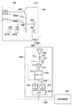
図1は、本発明の第1の実施形態の撮像素子を有する撮像装置の構成を示すブロック図である。撮像素子100は、受光部102、読み出し部103、制御部104、信号処理部105、出力部106を備えて構成される。受光部102は、複数の単位画素が行列状に配置されており、撮影レンズ101により結像された光学像を受光する。受光部102の構成については後述する。読出し部103は、制御部104の制御信号を受けて、受光部102から出力される画素信号をA/D変換し、信号処理部105に送る。
(First embodiment)
FIG. 1 is a block diagram illustrating a configuration of an imaging device having an imaging element according to the first embodiment of the present invention. The image sensor 100 includes a light receiving unit 102, a reading unit 103, a control unit 104, a signal processing unit 105, and an output unit 106. The light receiving unit 102 has a plurality of unit pixels arranged in a matrix, and receives an optical image formed by the imaging lens 101. The configuration of the light receiving unit 102 will be described later. The reading unit 103 receives the control signal from the control unit 104, A / D converts the pixel signal output from the light receiving unit 102, and sends the signal to the signal processing unit 105.

信号処理部105は、A/D変換された画像信号に対して、信号の加算、減算、乗算等の演算処理や、出力部106を介して撮像素子100から外部に出力する信号の選択処理などを行う。また、信号処理部105では、基準レベル調整等の各種補正やデータの並べ替えなども行う。これらの処理は、制御部104からの制御信号を受けて実行される。信号処理部105の詳細は後述するが、信号処理部105においては、受光部102から得られた画素信号に対して、撮像画像用の信号処理と焦点検出用の信号処理を行い、それらを出力部106に送る。出力部106は、信号処理部105により処理された画素信号を撮像素子100の外部に出力する。   The signal processing unit 105 performs arithmetic processing such as addition, subtraction, and multiplication of the A / D-converted image signal, and selection processing of a signal output from the image sensor 100 to the outside via the output unit 106. I do. The signal processing unit 105 also performs various corrections such as reference level adjustment, rearranges data, and the like. These processes are executed in response to a control signal from the control unit 104. Although the details of the signal processing unit 105 will be described later, the signal processing unit 105 performs signal processing for a captured image and signal processing for focus detection on the pixel signal obtained from the light receiving unit 102, and outputs them. Sent to the unit 106. The output unit 106 outputs the pixel signal processed by the signal processing unit 105 to the outside of the image sensor 100.

画像処理部107は、撮像素子100の出力部106から撮像画像用の信号を受け取り、欠陥画素の補正、ノイズリダクション、色変換、ホワイトバランス補正、画像補正等の画像処理や、解像度変換処理、画像圧縮処理などを行い、静止画像や動画像を生成する。位相差検出部108は、出力部106からの焦点検出用の信号を受けて、焦点検出を行うための位相差評価値を算出する。   The image processing unit 107 receives a signal for a captured image from the output unit 106 of the image sensor 100, and performs image processing such as correction of defective pixels, noise reduction, color conversion, white balance correction, image correction, resolution conversion processing, and image processing. A compression process or the like is performed to generate a still image or a moving image. The phase difference detection unit 108 receives a signal for focus detection from the output unit 106 and calculates a phase difference evaluation value for performing focus detection.

全体制御・演算部109は、撮像素子100や撮像装置全体の統括的な駆動及び制御を行う。表示部110は撮影後の画像やライブビュー画像、各種設定画面等を表示する。記録部111及びメモリ部112は、全体制御・演算部109から出力された画像信号等を記録保持する不揮発性メモリあるいはメモリカード等の記録媒体である。操作部113は撮像装置に備え付けられた操作部材によりユーザーの命令を受け付け、全体制御・演算回路106にその命令を入力する。レンズ制御部114は、位相差検出部108で算出された位相差評価値に基づいて光学系駆動情報を算出し、撮影レンズ101のフォーカスレンズ位置を制御する。   The overall control / arithmetic unit 109 performs overall driving and control of the imaging device 100 and the entire imaging device. The display unit 110 displays an image after photographing, a live view image, various setting screens, and the like. The recording unit 111 and the memory unit 112 are a recording medium such as a nonvolatile memory or a memory card that records and holds the image signal and the like output from the overall control / arithmetic unit 109. The operation unit 113 receives a user command from an operation member provided in the imaging apparatus, and inputs the command to the overall control / arithmetic circuit 106. The lens control unit 114 calculates optical system drive information based on the phase difference evaluation value calculated by the phase difference detection unit 108, and controls the focus lens position of the imaging lens 101.

次に、本実施形態の撮像装置における撮影レンズ101、マイクロレンズアレイ、撮像素子100の受光部102の関係と、画素の定義、及び瞳分割方式による焦点検出の原理について説明する。   Next, the relationship between the photographing lens 101, the microlens array, the light receiving unit 102 of the image sensor 100, the definition of pixels, and the principle of focus detection by the pupil division method in the image pickup apparatus of the present embodiment will be described.

図2は、撮像素子100の受光部102とマイクロレンズアレイを光軸方向(Z方向)から観察した図である。本実施形態では、マイクロレンズアレイを形成する個々のマイクロレンズ202を1つの画素と定義し、これを単位画素200とする。また、1つのマイクロレンズ202に対してフォトダイオード(PD)からなる2つの光電変換部がX軸方向に並んで配置されており、それぞれ光電変換部201A,201Bと定義する。   FIG. 2 is a diagram in which the light receiving unit 102 and the microlens array of the image sensor 100 are observed from the optical axis direction (Z direction). In this embodiment, each microlens 202 forming the microlens array is defined as one pixel, and this is defined as a unit pixel 200. In addition, two photoelectric conversion units including a photodiode (PD) are arranged side by side in the X-axis direction for one microlens 202, and are defined as photoelectric conversion units 201A and 201B, respectively.

図3は、撮影レンズ101を通過した光が1つのマイクロレンズ202を通過して撮像素子100の受光部102の単位画素200で受光される様子を光軸(Z軸)に対して垂直な方向(Y軸方向)から観察した図である。302,303は撮影レンズの射出瞳を表す。301はレンズ絞りである。射出瞳を通過した光は、光軸を中心として単位画素200に入射する。図3に示すように瞳領域302を通過する光束はマイクロレンズ202を通過して光電変換部201Aで受光され、瞳領域303を通過する光束はマイクロレンズ202を通して光電変換部201Bで受光される。したがって、光電変換部201A,201Bはそれぞれ撮影レンズの射出瞳の異なる領域の光を受光する。   FIG. 3 shows how light passing through the imaging lens 101 passes through one microlens 202 and is received by the unit pixel 200 of the light receiving unit 102 of the image sensor 100 in a direction perpendicular to the optical axis (Z axis). It is the figure observed from (Y-axis direction). Reference numerals 302 and 303 represent exit pupils of the photographing lens. Reference numeral 301 denotes a lens stop. The light that has passed through the exit pupil enters the unit pixel 200 about the optical axis. As shown in FIG. 3, a light beam passing through the pupil region 302 passes through the microlens 202 and is received by the photoelectric conversion unit 201A, and a light beam passing through the pupil region 303 is received by the photoelectric conversion unit 201B through the microlens 202. Therefore, the photoelectric conversion units 201A and 201B receive light in different areas of the exit pupil of the photographing lens.

撮影レンズ101からの光を瞳分割する光電変換部201Aの信号をX軸方向に並ぶ複数の単位画素200から取得し、これらの出力信号群で構成した被写体像をA像とする。同様に瞳分割する光電変換部201Bの信号をX軸方向に並ぶ複数の単位画素200から取得し、これらの出力信号群で構成した被写体像をB像とする。   A signal from the photoelectric conversion unit 201A that pupil-divides light from the photographing lens 101 is acquired from a plurality of unit pixels 200 arranged in the X-axis direction, and a subject image formed by these output signal groups is set as an A image. Similarly, a signal of the photoelectric conversion unit 201B that performs pupil division is obtained from a plurality of unit pixels 200 arranged in the X-axis direction, and a subject image formed by these output signal groups is set as a B image.

A像とB像に対して相関演算を実施し、像のずれ量(瞳分割位相差)を検出する。さらに像のずれ量に対して撮影レンズ101の焦点位置と光学系から決まる変換係数を乗じることで、画面内の任意の被写体位置に対応した焦点位置を算出することができる。ここで算出された焦点位置情報に基づいて撮影レンズ101のフォーカス位置を制御することで撮像面位相差AF(オートフォーカス)が可能となる。また、A像信号とB像信号との足し合わせをA+B像信号とすることで、このA+B像信号を通常の撮影画像に用いることができる。   The correlation calculation is performed on the A image and the B image to detect the image shift amount (pupil division phase difference). Further, by multiplying the image shift amount by a conversion coefficient determined by the focal position of the photographing lens 101 and the optical system, a focal position corresponding to an arbitrary subject position on the screen can be calculated. By controlling the focus position of the photographing lens 101 based on the focus position information calculated here, the imaging surface phase difference AF (autofocus) can be performed. Further, by adding the A image signal and the B image signal to an A + B image signal, the A + B image signal can be used for a normal captured image.

次に、撮像素子100の受光部102と読み出し部103の構成を図4、図5を用いて説明する。図4は、撮像素子100の受光部102と読出し部103の構成例を示すブロック図である。   Next, the configurations of the light receiving unit 102 and the reading unit 103 of the image sensor 100 will be described with reference to FIGS. FIG. 4 is a block diagram illustrating a configuration example of the light receiving unit 102 and the reading unit 103 of the image sensor 100.

受光部102は、画素部401と駆動回路部402とを有する。画素部401には複数の単位画素200が、水平方向(行方向)および垂直方向(列方向)に行列状に複数配列されている。図4においては単位画素200を2行3列の計6個図示しているが、実際は数百万、数千万の単位画素200が配置されている。駆動回路部402は画素部401を駆動するための電源回路、TG、走査回路などを含む。駆動回路部402によって駆動されて読み出された画素信号は、読み出し部103へ出力される。駆動回路部402は、図1の制御部104からの制御を受けて駆動される。読み出し部103には、画素部401からの画素信号が入力され、アナログデジタル変換(A/D変換)が行われる。なお、読出し部103は複数の読み出し回路、例えば1列に1つの読み出し回路を備えて構成される。   The light receiving unit 102 includes a pixel unit 401 and a driving circuit unit 402. In the pixel portion 401, a plurality of unit pixels 200 are arranged in a matrix in a horizontal direction (row direction) and a vertical direction (column direction). Although FIG. 4 shows a total of six unit pixels 200 in two rows and three columns, actually millions or tens of millions of unit pixels 200 are arranged. The driving circuit portion 402 includes a power supply circuit for driving the pixel portion 401, a TG, a scanning circuit, and the like. The pixel signal driven and read by the drive circuit unit 402 is output to the reading unit 103. The drive circuit unit 402 is driven under the control of the control unit 104 in FIG. The pixel signal from the pixel unit 401 is input to the reading unit 103, and analog-digital conversion (A / D conversion) is performed. Note that the reading unit 103 includes a plurality of reading circuits, for example, one reading circuit in one column.

図5は、撮像素子100の単位画素200、及び読み出し部103を構成する読み出し回路509の一例を示す図である。単位画素200において、フォトダイオード(PD)からなる光電変換部201Aには転送スイッチ502Aが接続され、光電変換部201Bには転送スイッチ502Bが接続される。光電変換部201A,201Bで発生した電荷は、それぞれ転送スイッチ502A,502Bを介して共通のフローティングディフュージョン部(FD)504に転送され、一時的に保存される。FD504に転送された電荷は、選択スイッチ506がオンされると、ソースフォロワアンプを形成する増幅MOSトランジスタ(SF)505を介して電荷に対応した電圧として列出力線507に出力される。列出力線507には電流源508が接続されている。   FIG. 5 is a diagram illustrating an example of the unit pixel 200 of the imaging element 100 and the readout circuit 509 included in the readout unit 103. In the unit pixel 200, a transfer switch 502A is connected to the photoelectric conversion unit 201A including a photodiode (PD), and a transfer switch 502B is connected to the photoelectric conversion unit 201B. The charges generated in the photoelectric conversion units 201A and 201B are transferred to a common floating diffusion unit (FD) 504 via transfer switches 502A and 502B, respectively, and are temporarily stored. When the selection switch 506 is turned on, the charge transferred to the FD 504 is output to the column output line 507 as a voltage corresponding to the charge via an amplification MOS transistor (SF) 505 forming a source follower amplifier. A current source 508 is connected to the column output line 507.

リセットスイッチ503は、FD504の電位、及び転送スイッチ502A,502Bを介して光電変換部201A,201Bの電位をVDDにリセットする。転送スイッチ502A,502B、リセットスイッチ503、選択スイッチ506は、それぞれ周辺の駆動回路部402に接続されている信号線を介して、制御信号PTXA、PTXB、PRES、PSELにより制御される。   The reset switch 503 resets the potential of the FD 504 and the potential of the photoelectric conversion units 201A and 201B to VDD via the transfer switches 502A and 502B. The transfer switches 502A and 502B, the reset switch 503, and the selection switch 506 are controlled by control signals PTXA, PTXB, PRES, and PSEL via signal lines connected to the peripheral drive circuit unit 402, respectively.

次に、読み出し回路509の回路構成について説明する。アンプ510は、列出力線507に現れた信号を増幅し、容量512は信号電圧を保持するために用いられる。容量512への書き込みは、制御信号PSHによりオン、オフされるスイッチ511により制御される。比較器513の一方の入力には、不図示のスロープ電圧発生回路から供給された参照電圧であるVslopeが入力され、他方の入力には、容量512に書き込まれたアンプ510の出力が入力される。比較器513はアンプ510の出力と参照電圧Vslopeを比較し、その大小関係によってローレベル、ハイレベルの2値のいずれかを出力する。具体的には、Vslopeがアンプ510の出力に対して小さい時にはローレベル、大きい時にはハイレベルを出力する。参照電圧Vslopeの遷移開始と同時にCLK(クロック)が動き出し、カウンタ514は比較器513の出力がハイレベルの時にCLKに対応してカウントアップし、比較器513の出力がローレベルに反転すると同時にカウントの信号を停止する。   Next, a circuit configuration of the reading circuit 509 is described. The amplifier 510 amplifies the signal appearing on the column output line 507, and the capacitor 512 is used to hold a signal voltage. Writing to the capacitor 512 is controlled by a switch 511 which is turned on / off by a control signal PSH. One input of the comparator 513 receives a reference voltage Vslope supplied from a slope voltage generating circuit (not shown), and the other input receives an output of the amplifier 510 written in the capacitor 512. . The comparator 513 compares the output of the amplifier 510 with the reference voltage Vslope and outputs one of a low level and a high level according to the magnitude relation. Specifically, when Vslope is smaller than the output of the amplifier 510, a low level is output, and when Vslope is higher, a high level is output. When the output of the comparator 513 is at the high level, the counter 514 counts up in response to the CLK when the output of the comparator 513 is at the high level, and counts at the same time when the output of the comparator 513 is inverted to the low level. Stop the traffic light.

メモリ516には、FD504のリセットレベルの信号(以下、「N信号」)をAD変換したデジタル信号が保持され、メモリ517には、光電変換部201Aや光電変換部201Bの信号をFD504のN信号に重畳した信号(以下「S信号」)をAD変換したデジタル信号が保持される。メモリ516,517のどちらに書き込まれるかはスイッチ515により振り分けられる。メモリ516,517に保持された信号はCDS回路518にてS信号からN信号を差し引いた差分が算出される。そして、駆動回路部402の制御により、デジタル信号出力線519を介して信号処理部105へ出力される。   The memory 516 holds a digital signal obtained by AD-converting the reset level signal (hereinafter, “N signal”) of the FD 504, and the memory 517 stores the signal of the photoelectric conversion unit 201A or 201B in the N signal of the FD 504. A digital signal obtained by AD-converting a signal (hereinafter, referred to as “S signal”) superimposed on the digital signal is held. Which of the memories 516 and 517 is written is determined by the switch 515. For the signals held in the memories 516 and 517, the CDS circuit 518 calculates a difference obtained by subtracting the N signal from the S signal. Then, under the control of the drive circuit unit 402, the signal is output to the signal processing unit 105 via the digital signal output line 519.

なお、読み出し回路509は画素の各列に対して1つ配置され、画素信号は行単位で読み出される。この場合、選択スイッチ506は行単位で制御され、選択された行の画素信号が一括して列出力線507に出力される。この読み出し回路509の数が多いほど、画素部401の画素信号を高速に信号処理部105に読み出すことができる。   Note that one read circuit 509 is provided for each column of pixels, and pixel signals are read in units of rows. In this case, the selection switch 506 is controlled in units of rows, and the pixel signals of the selected row are output to the column output line 507 collectively. As the number of the readout circuits 509 increases, the pixel signals of the pixel portion 401 can be read out to the signal processing portion 105 at higher speed.

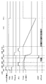
図6は、図5に示す回路構成を有する撮像素子100の単位画素200からの電荷読み出し動作の一例を示すタイミングチャートである。各駆動パルスのタイミング、参照電圧Vslope、CLK、水平走査信号を模式的に示している。また、各タイミングにおける列出力線の電位Vlも併せて示している。   FIG. 6 is a timing chart showing an example of the operation of reading out charges from the unit pixels 200 of the image sensor 100 having the circuit configuration shown in FIG. The timing of each drive pulse, the reference voltages Vslope, CLK, and the horizontal scanning signal are schematically shown. The potential Vl of the column output line at each timing is also shown.

光電変換部201Aからの信号の読み出しに先立って、リセットスイッチ503の信号線PRESがHiとなる(t600)。これによって、SF(ソースフォロワアンプ)505のゲートがリセット電源電圧にリセットされる。時刻t601で制御信号PSELをHiとし、SF505を動作状態とする。そして、t602で制御信号PRESをLoとすることでFD504のリセットを解除する。このときのFD504の電位を列出力線507にリセット信号レベル(N信号)として読み出し、読み出し回路509に入力する。   Prior to reading of a signal from the photoelectric conversion unit 201A, the signal line PRES of the reset switch 503 becomes Hi (t600). As a result, the gate of the SF (source follower amplifier) 505 is reset to the reset power supply voltage. At time t601, the control signal PSEL is set to Hi, and the SF 505 is set to the operating state. Then, the reset of the FD 504 is released by setting the control signal PRES to Lo at t602. The potential of the FD 504 at this time is read out to the column output line 507 as a reset signal level (N signal), and is input to the reading circuit 509.

時刻t603、t604で制御信号PSHをHi、Loとしてスイッチ511をオン、オフすることで、列出力線507に読み出されたN信号はアンプ510で所望のゲインで増幅されたのち容量512に保持される。容量512に保持されたN信号の電位は比較器513の一方に入力される。時刻t604でスイッチ511がオフされた後、時刻t605からt607まで、不図示のスロープ電圧発生回路により、参照電圧Vslopeを時刻と共に初期値から減少させていく。参照電圧Vslopeの遷移開始と共に、CLK(クロック)をカウンタ514に供給する。CLKの数に応じてカウンタ514の値は増加していく。そして、比較器513に入力した参照電圧VslopeがN信号と同じレベルになると、比較器513の出力COMPはローレベルとなり、同時にカウンタ514の動作も停止する(時刻t606)。この、カウンタ514の動作が停止した時の値が、N信号がAD変換された値となり、スイッチ515により、カウンタ514とメモリ516が接続され、N信号のデジタル値がN信号用メモリ516に保持される。   At time t603 and t604, the control signal PSH is set to Hi and Lo to turn on and off the switch 511, so that the N signal read out to the column output line 507 is amplified by the amplifier 510 with a desired gain and then stored in the capacitor 512. Is done. The potential of the N signal held in the capacitor 512 is input to one of the comparators 513. After the switch 511 is turned off at time t604, from time t605 to t607, the slope voltage generation circuit (not shown) decreases the reference voltage Vslope from the initial value with time. When the transition of the reference voltage Vslope starts, CLK (clock) is supplied to the counter 514. The value of the counter 514 increases according to the number of CLKs. Then, when the reference voltage Vslope input to the comparator 513 becomes the same level as the N signal, the output COMP of the comparator 513 becomes low level, and at the same time, the operation of the counter 514 stops (time t606). The value when the operation of the counter 514 is stopped becomes the value obtained by AD-converting the N signal. The counter 514 and the memory 516 are connected by the switch 515, and the digital value of the N signal is held in the N-signal memory 516. Is done.

次に、デジタル化されたN信号をN信号メモリ516に保持した後の時刻t607、t608で制御信号PTXAを順次Hi、Loとして光電変換部201Aに蓄積された光電荷をFD504に転送する。すると、電荷量に応じたFD504の電位変動が列出力線507に信号レベル(光成分+リセットノイズ成分(N信号))として読み出され、読み出し回路509に入力される。入力された信号(S(A)+N)はアンプ510で所望のゲインで増幅されたのち、時刻t609、t610で制御信号PSHを順次Hi、Loとしてスイッチ511をオン、オフするタイミングで容量512に保持される。容量512に保持された電位は比較器513の一方に入力される。時刻t610でスイッチ511がオフされた後、時刻t611からt613まで、スロープ電圧発生回路により、参照電圧Vslopeを時刻と共に初期値から減少させていく。参照電圧Vslopeの遷移開始と共に、CLKをカウンタ514に供給する。CLKの数に応じてカウンタ514の値は増加していく。そして、比較器513に入力した参照電圧VslopeがS信号と同じレベルになると、比較器513の出力COMPはローレベルとなり、同時にカウンタ514の動作も停止する(時刻t612)。この、カウンタ514の動作が停止した時の値が、S(A)+N信号がAD変換された値となる。そして、スイッチ515により、カウンタ514とメモリ517が接続され、S(A)+N信号のデジタル値がS信号用メモリ517に保持される。メモリ516及びメモリ517に保持された信号からCDS回路518により差動信号レベル(光成分)が算出され、リセットノイズ成分が除去されたS(A)信号が得られる。S(A)信号は、制御部104の制御により順次信号処理部105に送られる。   Next, at times t607 and t608 after the digitized N signal is stored in the N signal memory 516, the control signal PTXA is sequentially set to Hi and Lo, and the optical charge accumulated in the photoelectric conversion unit 201A is transferred to the FD 504. Then, the potential variation of the FD 504 according to the charge amount is read out to the column output line 507 as a signal level (light component + reset noise component (N signal)) and input to the reading circuit 509. The input signal (S (A) + N) is amplified by the amplifier 510 with a desired gain, and then at time t609 and t610, the control signal PSH is sequentially set to Hi and Lo to turn on and off the switch 511 and then to the capacitor 512 at the timing. Will be retained. The potential held in the capacitor 512 is input to one of the comparators 513. After the switch 511 is turned off at time t610, the reference voltage Vslope is reduced from the initial value with time by the slope voltage generation circuit from time t611 to t613. When the transition of the reference voltage Vslope starts, CLK is supplied to the counter 514. The value of the counter 514 increases according to the number of CLKs. Then, when the reference voltage Vslope input to the comparator 513 becomes the same level as the S signal, the output COMP of the comparator 513 becomes low level, and the operation of the counter 514 stops at the same time (time t612). The value when the operation of the counter 514 is stopped is a value obtained by AD-converting the S (A) + N signal. Then, the counter 514 and the memory 517 are connected by the switch 515, and the digital value of the S (A) + N signal is held in the S signal memory 517. The CDS circuit 518 calculates the differential signal level (light component) from the signals held in the memories 516 and 517, and obtains the S (A) signal from which the reset noise component has been removed. The S (A) signal is sequentially sent to the signal processing unit 105 under the control of the control unit 104.

以上が、単位画素200の光電変換部201Aからの信号を読み出す動作である。単位画素200のもう一方の光電変換部201Bからの信号を読み出す場合も同様に図6のタイミングチャートに従って駆動すればよい。ただし、この場合はt607、t608において制御信号PTXAの代わりにPTXBを順次Hi、Loする。すなわち、図6のt600からt613の駆動を1回目に制御信号PTXAをHi、Loして画素信号S(A)を読出し、続いて2回目に制御信号PTXBをHi、Loして画素信号S(B)を読み出すことで、1行の読み出しが完了する。これを全行分繰り返すことで、全画素の画素信号S(A)、S(B)の読み出しが完了する。   The above is the operation of reading the signal from the photoelectric conversion unit 201A of the unit pixel 200. Similarly, when reading a signal from the other photoelectric conversion unit 201B of the unit pixel 200, driving may be performed according to the timing chart of FIG. However, in this case, PTXB is sequentially Hi and Lo instead of the control signal PTXA at t607 and t608. That is, the control signal PTXA is set to Hi and Lo for the first time to drive the pixel signal S (A) from t600 to t613 in FIG. 6, and the control signal PTXB is set to Hi and Lo for the second time to drive the pixel signal S ( By reading B), reading of one row is completed. By repeating this for all rows, the reading of the pixel signals S (A) and S (B) of all pixels is completed.

図7は、撮像素子100の信号処理部105及び出力部106の構成例を示す図である。信号処理部105は撮像画像用信号処理部701と焦点検出用信号処理部702を有する。読み出し部103から出力された画素信号はデジタル信号出力線519を介して信号処理部105に入力される。入力された信号は制御部104からの制御に従って処理される。なお、撮像画像用信号処理部701と焦点検出用信号処理部702は、それぞれ不図示のメモリを備えるものとする。   FIG. 7 is a diagram illustrating a configuration example of the signal processing unit 105 and the output unit 106 of the image sensor 100. The signal processing unit 105 includes a captured image signal processing unit 701 and a focus detection signal processing unit 702. The pixel signal output from the reading unit 103 is input to the signal processing unit 105 via the digital signal output line 519. The input signal is processed under the control of the control unit 104. Note that the captured image signal processing unit 701 and the focus detection signal processing unit 702 each include a memory (not shown).

撮像画像用信号処理部701では、読み出された信号から、撮像画像用信号を算出する。すなわち、単位画素200の光電変換部201A、及び光電変換部201Bの画素信号S(A)、S(B)を受けて、混合処理を行い、S(A+B)信号を算出する。そして、画素信号S(A+B)を撮像画像用信号出力線703を介して出力部106に送る。撮像画像用信号処理部701において、2つの光電変換部の画素信号S(A)、S(B)を混合処理して出力部106から撮像素子100の外部に出力することで、撮像素子100の外部への信号伝送量を減らすことができる。なお、画素信号S(A)とS(B)の演算は、単位画素の両方の信号がそろった段階で可能となる。先に読み出された画素信号S(A)はメモリで保持しておき、画素信号S(B)が読み出され、撮像画像用信号処理部701に入力されると、順次S(A)+S(B)が演算され、出力部106から出力される。   The captured image signal processing unit 701 calculates a captured image signal from the read signal. That is, upon receiving the pixel signals S (A) and S (B) of the photoelectric conversion unit 201A and the photoelectric conversion unit 201B of the unit pixel 200, a mixing process is performed to calculate an S (A + B) signal. Then, the pixel signal S (A + B) is sent to the output unit 106 via the captured image signal output line 703. In the captured image signal processing unit 701, the pixel signals S (A) and S (B) of the two photoelectric conversion units are mixed and output from the output unit 106 to the outside of the image sensor 100, so that the image sensor 100 The amount of signal transmission to the outside can be reduced. The calculation of the pixel signals S (A) and S (B) can be performed when both signals of the unit pixel are completed. The previously read pixel signal S (A) is stored in a memory, and when the pixel signal S (B) is read and input to the captured image signal processing unit 701, the pixel signal S (A) + S (B) is calculated and output from the output unit 106.

なお、撮像画像用信号処理部では更に単位画素200同士の信号を混合、平均化処理してもよい。例えば、赤(R)、緑(G)、青(B)のベイヤ―配列のカラーフィルタが設けられた一般的な構成の画素部において、隣接する同色画素の信号を混合平均化演算して出力部106に送れば、更に信号伝送量を減らすことができる。また、画素部全ての信号を出力部106に出力するのではなく、必要な領域のみの信号を出力してもよい。これらの処理は制御部104により制御される。   Note that the captured image signal processing unit may further mix and average the signals of the unit pixels 200. For example, in a pixel portion having a general configuration in which color filters of a Bayer array of red (R), green (G), and blue (B) are provided, signals of adjacent pixels of the same color are mixed and averaged and output. Sending to unit 106 can further reduce the amount of signal transmission. Further, instead of outputting all the signals of the pixel portion to the output unit 106, signals of only a necessary region may be output. These processes are controlled by the control unit 104.

続いて、焦点検出用信号処理部702の処理について説明する。焦点検出用信号処理部702では、読み出された信号から、焦点検出用信号を算出して出力する。位相差検出を行うためには、前述した通り、画素信号S(A)とS(B)がそれぞれ必要である。しかし、画素部401の全ての画素の画素信号S(A)とS(B)を出力部106から撮像素子100の外部に出力するとなると信号伝送量が膨大になり、高速読み出しに望ましくない。   Subsequently, the processing of the focus detection signal processing unit 702 will be described. The focus detection signal processing unit 702 calculates and outputs a focus detection signal from the read signal. To detect the phase difference, the pixel signals S (A) and S (B) are required as described above. However, when the pixel signals S (A) and S (B) of all the pixels of the pixel unit 401 are output from the output unit 106 to the outside of the image sensor 100, the signal transmission amount becomes enormous, which is not desirable for high-speed reading.

そこで、焦点検出用信号処理部702において演算処理を行い、信号量を減らして出力部106から出力する。例えば、画素信号S(A)、S(B)をそれぞれベイヤ加算して輝度値Y値を算出して、輝度信号Y(A)、Y(B)を出力する。焦点検出演算は、信号をY値に変換してから演算することもあり、撮像素子100から出力する前にY値を演算することで、信号伝送量を1/4に減らすことができる。なお、Y値の演算にはベイヤ単位の信号が必要になるため、演算に必要な信号が揃うまで、焦点検出用信号処理部702に入力された画素信号をメモリに保持しておく。つまり、R・G行の信号が読み出された後、G・B行の信号が読み出されるので、R・G行の画素信号S(A)とS(B)はメモリに保持しておき、G・B行の信号が読み出されたら順次輝度信号Y(A)、Y(B)を演算し、信号線704を介して出力部106から出力する。   Therefore, arithmetic processing is performed in the focus detection signal processing unit 702 to reduce the signal amount and output the signal from the output unit 106. For example, a luminance value Y value is calculated by Bayer addition of the pixel signals S (A) and S (B), and the luminance signals Y (A) and Y (B) are output. The focus detection calculation may be performed after converting the signal into a Y value, and by calculating the Y value before outputting the signal from the image sensor 100, the signal transmission amount can be reduced to 4. Note that since the calculation of the Y value requires a signal in Bayer units, the pixel signals input to the focus detection signal processing unit 702 are held in the memory until the signals necessary for the calculation are completed. That is, since the signals on the G and B rows are read after the signals on the R and G rows are read out, the pixel signals S (A) and S (B) on the R and G rows are stored in the memory, When the signals in the G and B rows are read, the luminance signals Y (A) and Y (B) are sequentially calculated and output from the output unit 106 via the signal line 704.

また、更に焦点検出用信号処理部702において相関演算を行い、その演算値を信号線704から出力部106に出力してもよい。なお、相関演算を用いた位相差検出は公知の手法により実施可能である。相関演算値のみの出力であれば、その演算時の領域分割数に依存するものの、出力する信号量は大幅に減らすことができる。   Further, a correlation operation may be performed in the focus detection signal processing unit 702, and the operation value may be output to the output unit 106 from the signal line 704. The phase difference detection using the correlation operation can be performed by a known method. If only the correlation operation value is output, the output signal amount can be significantly reduced although it depends on the number of area divisions at the time of the operation.

以上のように、撮像画像用信号処理部701と焦点検出用信号処理部702を備える撮像素子100において、必要な信号のみを撮像素子100の外部に出力する信号処理を行う。これにより、信号伝送量を減らすことができ、撮像画像データと焦点検出情報を共に高速に得ることができる。   As described above, in the imaging device 100 including the captured image signal processing unit 701 and the focus detection signal processing unit 702, signal processing for outputting only necessary signals to the outside of the imaging device 100 is performed. As a result, the amount of signal transmission can be reduced, and both the captured image data and the focus detection information can be obtained at high speed.

なお、本実施形態においては、撮像画像用信号処理部701と焦点検出用信号処理部702それぞれにメモリを備える構成とした。しかし、これらの前段にメモリを備えて、各処理部における演算に必要な信号が揃った段階で、撮像画像用信号処理部701と焦点検出用信号処理部702に信号を送る構成であってもよい。   In this embodiment, each of the captured image signal processing unit 701 and the focus detection signal processing unit 702 includes a memory. However, a configuration is also possible in which a memory is provided in the preceding stage and signals are sent to the captured image signal processing unit 701 and the focus detection signal processing unit 702 when the signals necessary for calculation in each processing unit are prepared. Good.

また、本実施形態の説明において、焦点検出用信号として、輝度信号Y(A)、及びY(B)を出力したが、出力部106からは輝度信号Y(A)のみを出力してもよい。具体的には、撮像画像用信号処理部701からは、撮像画像用信号、すなわち画素信号S(A+B)が出力されている。そのため、撮像素子100の外部に出力された後、位相差検出部108などで画素信号S(A+B)から輝度信号Y(A+B)を演算し、輝度信号Y(A)の減算処理を行い、輝度信号Y(B)を算出することで、焦点検出用信号を得てもよい。このように、焦点検出用信号処理部702からは輝度信号Y(A)のみを出力することによって、信号伝送量を更に減らすことができる。   In the description of the present embodiment, the luminance signals Y (A) and Y (B) are output as focus detection signals. However, the output unit 106 may output only the luminance signal Y (A). . Specifically, the captured image signal processing unit 701 outputs a captured image signal, that is, a pixel signal S (A + B). Therefore, after being output to the outside of the image sensor 100, the luminance signal Y (A + B) is calculated from the pixel signal S (A + B) by the phase difference detection unit 108 or the like, and the luminance signal Y (A) is subtracted. The signal for focus detection may be obtained by calculating the signal Y (B). In this way, by outputting only the luminance signal Y (A) from the focus detection signal processing unit 702, the signal transmission amount can be further reduced.

例えば、画素数が2000万画素であった場合、信号処理部を備えない場合は全画素分の画素信号S(A)、S(B)、すなわち4000万個のデータを出力する必要がある。一方、本実施形態の信号処理部を備える撮像素子により焦点検出用信号としてY値を演算して出力する場合、撮像画像用の2000万個のデータと焦点検出用の2000万/4=500万個のデータを出力することになり、信号伝送量が減ることがわかる。その結果、高速読み出しが可能となる。また、焦点検出用信号が相関演算値である場合、更に信号伝送量が減ることは明らかである。   For example, if the number of pixels is 20 million pixels, and if no signal processing unit is provided, it is necessary to output pixel signals S (A) and S (B) for all pixels, that is, 40 million data. On the other hand, when the Y value is calculated and output as a focus detection signal by the imaging device including the signal processing unit of the present embodiment, 20 million data for a captured image and 20,000,000 / 4 = 5,000,000 for focus detection This means that the number of pieces of data to be output indicates that the signal transmission amount is reduced. As a result, high-speed reading becomes possible. When the focus detection signal is a correlation operation value, it is apparent that the signal transmission amount is further reduced.

また、図6のタイミングチャートにおいて、t607、t608で制御信号PTXA、PTXBを同時に制御して光電変換部201Aと光電変換部201Bの電荷が混合された単位画素200の信号を得ることも可能である。具体的には、図6のタイミングチャートに従って、光電変換部201Aの信号を読み出した後、制御信号PTXA、PTXBを同時にHi、Lo制御して信号を読み出せば画素信号S(A+B)を得ることが可能である。この場合、リセット信号の読み出しが1回減るため、更に高速読み出しが可能となる。   In the timing chart of FIG. 6, it is also possible to simultaneously control the control signals PTXA and PTXB at t607 and t608 to obtain a signal of the unit pixel 200 in which the charges of the photoelectric conversion units 201A and 201B are mixed. . Specifically, according to the timing chart of FIG. 6, after reading the signal of the photoelectric conversion unit 201A, the control signals PTXA and PTXB are simultaneously controlled to Hi and Lo to read out the signal, thereby obtaining the pixel signal S (A + B). Is possible. In this case, the reading of the reset signal is reduced by one, so that a higher-speed reading can be performed.

画素から画素信号S(A)とS(A+B)が読み出された場合には、焦点検出用信号処理部702において、画素信号S(A+B)から画素信号S(A)を減算する処理を行えば、画素信号S(B)を得ることができる。もしくは、焦点検出処理部702においては、画素信号S(A)のみ処理して出力し、位相差検出部108で画素信号S(B)あるいは輝度信号Y(B)の算出を行ってもよい。   When the pixel signals S (A) and S (A + B) are read from the pixel, the focus detection signal processing unit 702 performs a process of subtracting the pixel signal S (A) from the pixel signal S (A + B). For example, a pixel signal S (B) can be obtained. Alternatively, the focus detection processing unit 702 may process and output only the pixel signal S (A), and the phase difference detection unit 108 may calculate the pixel signal S (B) or the luminance signal Y (B).

(第2の実施形態)
次に、本発明の第2の実施形態について説明する。第1の実施形態においては、画素部の全領域において焦点検出用信号の出力を行ったが、焦点検出用信号については必要な領域のみの信号を選択して出力すれば、更に高速化を実現することができる。
(Second embodiment)
Next, a second embodiment of the present invention will be described. In the first embodiment, the focus detection signal is output in the entire area of the pixel portion. However, if the focus detection signal is selected and output only from a necessary area, the speed can be further increased. can do.

図8は、画素領域における、焦点検出用信号の出力領域の例を示した図である。斜線で示した領域は、焦点検出用信号と撮像画像用信号を出力し、それ以外の領域は撮像画像用信号のみを出力する。例えば、図8(a)に示した例のように、画素の広範囲において目的とする領域のみの焦点検出用信号を離散的に(選択的に)出力する。これによって、画素領域全体の焦点検出情報を得ることが可能となる一方で、撮像素子100の外部に出力する信号量を抑制することが可能となる。また、図8(b)に示した例の場合、一部の領域について詳細な焦点検出情報を得ることが可能となり、また撮像素子100の外部に出力する信号量を抑制することが可能となる。これらの出力する領域の選択は制御部104により制御される。焦点検出用信号処理部702において、出力対象領域の信号のみをメモリから読み出して演算する。   FIG. 8 is a diagram illustrating an example of an output area of a focus detection signal in a pixel area. The hatched area outputs the focus detection signal and the captured image signal, and the other areas output only the captured image signal. For example, as in the example shown in FIG. 8A, a focus detection signal for only a target area in a wide range of pixels is discretely (selectively) output. Thereby, while it is possible to obtain the focus detection information of the entire pixel region, it is possible to suppress the amount of signals output to the outside of the image sensor 100. In the case of the example shown in FIG. 8B, it is possible to obtain detailed focus detection information for a part of the area, and it is possible to suppress the amount of signals output to the outside of the image sensor 100. . The selection of these output areas is controlled by the control unit 104. In the focus detection signal processing unit 702, only the signal of the output target area is read from the memory and calculated.

なお、図8に示したような一部の領域における焦点検出用信号の出力は、Y値信号や相関演算結果でもよいが、画素信号S(A)であってもよい。Y値信号や相関演算結果に比べて伝送する信号量は多くなるが、必要領域のみ出力するため、信号伝送量の抑制は達成される。また、比較的小規模な信号処理回路でも実現可能である。   Note that the output of the focus detection signal in a part of the region as shown in FIG. 8 may be a Y-value signal or a correlation operation result, or may be a pixel signal S (A). Although the amount of signal to be transmitted is larger than that of the Y-value signal and the result of the correlation operation, since only the necessary area is output, suppression of the signal transmission amount is achieved. Further, it can be realized by a relatively small-scale signal processing circuit.

なお、焦点検出用信号処理部702においても、焦点検出用信号を混合、平均化処理してもよい。この場合、画素信号S(A)同士、画素信号S(B)同士について混合、平均化処理を行う。   Note that the focus detection signal processing unit 702 may also mix and average the focus detection signals. In this case, the pixel signals S (A) and the pixel signals S (B) are mixed and averaged.

以上のように、撮像画像用信号処理部701と焦点検出用信号処理部702を備える撮像素子100において、必要な信号のみを撮像素子100の外部に出力する信号処理を行う。これにより、焦点検出用信号の伝送量を減らすことができ、撮像画像データと焦点検出情報を共に高速かつ効率的に得ることができる。   As described above, in the imaging device 100 including the captured image signal processing unit 701 and the focus detection signal processing unit 702, signal processing for outputting only necessary signals to the outside of the imaging device 100 is performed. Thus, the transmission amount of the focus detection signal can be reduced, and both the captured image data and the focus detection information can be obtained quickly and efficiently.

なお、このように焦点検出に使用する画素を限定することによって、1フレームの読み出し時間を短縮する方法がある。通常は、焦点検出処理に使用する行のみ単位画素内の2つの光電変換部の信号をそれぞれ読み出し、焦点検出処理に使用しない行は2つの光電変換部の信号を混合して画像生成用の信号のみを読み出すことで読み出し時間の増大を抑制する。この場合、焦点検出用として読み出された2つの光電変換部の個々の出力信号は混合して撮像画像用の画素信号として使用することが可能である。しかし、信号の読み出し方法や2つの光電変換部の出力信号の混合方法が焦点検出処理に使用する行としない行とで異なることにより、ノイズレベル等に差が生じてしまい、その結果得られる撮像画像が劣化するという問題が生じる。しかし、本実施形態のように焦点検出用信号処理部を備えることによって、画素部からの信号は全て同様の読み出しタイミングで読み出し、焦点検出用信号処理部702で出力する画素を選択できる。そのため、撮像画像に用いる画素信号S(A+B)のノイズ量が領域によって異なることもなく、高品質の撮像画像を得ることができる。   Note that there is a method of shortening the reading time of one frame by limiting the pixels used for focus detection in this way. Normally, the signals of the two photoelectric conversion units in the unit pixel are read out only for the rows used for the focus detection processing, and the signals for the image generation are mixed for the rows not used for the focus detection processing by mixing the signals of the two photoelectric conversion units. By reading only the data, an increase in read time is suppressed. In this case, the individual output signals of the two photoelectric conversion units read for focus detection can be mixed and used as a pixel signal for a captured image. However, since the method of reading signals and the method of mixing output signals of the two photoelectric conversion units are different between a row used for focus detection processing and a row not used for focus detection processing, a difference occurs in noise level and the like, and the resulting imaging There is a problem that the image is deteriorated. However, by providing the focus detection signal processing unit as in the present embodiment, all signals from the pixel unit can be read out at the same readout timing, and a pixel to be output by the focus detection signal processing unit 702 can be selected. Therefore, a high-quality captured image can be obtained without the noise amount of the pixel signal S (A + B) used for the captured image being different depending on the region.

(第3の実施形態)
次に、本発明の第3の実施形態について説明する。第3の実施形態では、画素部402の単位画素200の構成が異なる。図9は、撮像素子100の受光部102及びマイクロレンズアレイを光軸方向(Z方向)から観察した図である。1つのマイクロレンズ202に対して、4つの光電変換部901A、901B、901C、901Dが配置されている。このように、X軸方向及びY軸方向それぞれ2つの合計4つの光電変換部を有することで、4つに分割された射出瞳領域の光をそれぞれ受光することができる。このような単位画素がそれぞれ4つの光電変換部を備えている画素部401により構成される撮像素子100における、信号読み出し方法、及び信号処理部105の処理について説明する。
(Third embodiment)
Next, a third embodiment of the present invention will be described. In the third embodiment, the configuration of the unit pixel 200 of the pixel unit 402 is different. FIG. 9 is a diagram in which the light receiving unit 102 and the microlens array of the image sensor 100 are observed from the optical axis direction (Z direction). Four photoelectric conversion units 901A, 901B, 901C, and 901D are arranged for one microlens 202. In this manner, by having a total of four photoelectric conversion units in each of the X-axis direction and the Y-axis direction, light in the exit pupil region divided into four can be respectively received. A signal reading method and a process of the signal processing unit 105 in the imaging device 100 including the pixel unit 401 in which each of the unit pixels includes four photoelectric conversion units will be described.

図10は、単位画素900及び読み出し部103の構成の一例を示す模式図である。図10の構成では、各光電変換部のそれぞれに読み出し回路を備えている。すなわち、光電変換部901Aの画素信号は読み出し回路1001Aにより読み出される。以下同様に、光電変換部901Bは読み出し回路1001B、光電変換部901Cは読み出し回路1001C、光電変換部901Dは読み出し回路1001Dにより読み出される。光電変換部からの信号読み出し動作については、図5、図6で説明した駆動方法とほぼ同様の方法で実施可能であるため、説明は省略する。   FIG. 10 is a schematic diagram illustrating an example of a configuration of the unit pixel 900 and the reading unit 103. In the configuration of FIG. 10, each photoelectric conversion unit is provided with a readout circuit. That is, the pixel signal of the photoelectric conversion unit 901A is read by the reading circuit 1001A. Similarly, the readout circuit 1001B reads the photoelectric conversion unit 901B, the readout circuit 1001C reads the photoelectric conversion unit 901C, and the readout circuit 1001D reads the photoelectric conversion unit 901D. The operation of reading signals from the photoelectric conversion unit can be performed by a method substantially similar to the driving method described with reference to FIGS. 5 and 6, and a description thereof will be omitted.

各光電変換部から読み出された信号に対する信号処理部105の処理について説明する。撮像画像用信号処理部701では、読み出された信号から、撮像画像用信号を算出する。すなわち、単位画素900の複数の光電変換部901A、901B、901C、901Dの画素信号S(A)、S(B)、S(C)、S(D)を受けて、混合処理を行い、画素信号S(A+B+C+D)を算出する。そして、画素信号S(A+B+C+D)を撮像画像用信号出力線703を介して出力部106に送る。撮像画像用信号処理部701において、複数の光電変換部の信号を混合処理して出力部106から撮像素子100の外部に出力することで、撮像素子100の外部への信号伝送量を減らすことができる。単位画素900のように4つの光電変換部を備えるような撮像素子においては、その効果はより大きくなる。   The processing of the signal processing unit 105 for the signal read from each photoelectric conversion unit will be described. The captured image signal processing unit 701 calculates a captured image signal from the read signal. That is, the pixel signals S (A), S (B), S (C), and S (D) of the plurality of photoelectric conversion units 901A, 901B, 901C, and 901D of the unit pixel 900 are received, and a mixing process is performed. The signal S (A + B + C + D) is calculated. Then, the pixel signal S (A + B + C + D) is sent to the output unit 106 via the captured image signal output line 703. In the captured image signal processing unit 701, signals from a plurality of photoelectric conversion units are mixed and output from the output unit 106 to the outside of the image sensor 100, so that the amount of signal transmission to the outside of the image sensor 100 can be reduced. it can. In an image sensor having four photoelectric conversion units, such as the unit pixel 900, the effect is further enhanced.

続いて、焦点検出用信号処理部702の処理について説明する。図9に示した様な単位画素900当たり4つの光電変換部を備える撮像素子の場合、焦点検出のためには4つの光電変換部の信号を個別に読み出す必要があり、信号伝送量が膨大になり、高速読み出しに望ましくない。第1の実施形態で説明したように、Y値を演算して出力したり、相関演算結果のみを出力することが好適である。必要な領域のみの信号を出力すれば、更に信号伝送量を減らすことができる。   Subsequently, the processing of the focus detection signal processing unit 702 will be described. In the case of an image sensor having four photoelectric conversion units per unit pixel 900 as shown in FIG. 9, it is necessary to read out the signals of the four photoelectric conversion units individually for focus detection, and the signal transmission amount is enormous. This is not desirable for high-speed reading. As described in the first embodiment, it is preferable to calculate and output the Y value or to output only the correlation calculation result. By outputting a signal only in a necessary area, the amount of signal transmission can be further reduced.

また、図9のように単位画素900が2x2の光電変換部を備える構成の場合、左右方向に加え、上下方向の位相差検出も行うことができる。例えば、画素信号S(A)とS(C)を混合処理し、画素信号S(B)とS(D)を混合処理してそれぞれ出力する。この場合、得られた焦点検出用信号からは左右方向に瞳分割された位相差方式の焦点検出が可能となる。また、画素信号S(A)とS(B)を混合処理し、画素信号S(C)とS(D)を混合処理してそれぞれ出力した場合は、得られた焦点検出用信号からは上下方向に瞳分割された位相差方式の焦点検出が可能となる。これらは、被写体に応じて切り替えて出力することで、縦縞、横縞それぞれの被写体に対して精度良く焦点検出することができる。また、画素の領域によって出力パターンを変えてもよい。   In the case where the unit pixel 900 includes a 2 × 2 photoelectric conversion unit as shown in FIG. 9, the phase difference can be detected not only in the horizontal direction but also in the vertical direction. For example, the pixel signals S (A) and S (C) are mixed and the pixel signals S (B) and S (D) are mixed and output. In this case, it is possible to perform focus detection by the phase difference method in which the pupil is divided in the left-right direction from the obtained focus detection signal. Further, when the pixel signals S (A) and S (B) are mixed and the pixel signals S (C) and S (D) are mixed and output, the obtained focus detection signals are vertically shifted. It is possible to perform focus detection by the phase difference method in which the pupil is divided in the direction. By switching and outputting these in accordance with the subject, it is possible to accurately perform focus detection on the subject of each of vertical stripes and horizontal stripes. Further, the output pattern may be changed depending on the pixel area.

更に、焦点検出用信号処理部702において、得られた混合信号(例えば、S(A+C)とS(B+D))を用いて相関演算を行い、その結果のみを出力してもよい。焦点検出用信号処理部702で相関演算処理をすれば撮像素子100から出力する信号伝送量を減らすことができる。また、同一領域において左右方向と上下方向両方の相関演算を行って出力しても信号伝送量を抑えることができる。   Further, the focus detection signal processing unit 702 may perform a correlation operation using the obtained mixed signals (for example, S (A + C) and S (B + D)) and output only the result. If the correlation calculation processing is performed by the focus detection signal processing unit 702, the amount of signal output from the image sensor 100 can be reduced. Further, even if the correlation operation is performed in both the left and right directions and the up and down directions in the same area, the signal transmission amount can be suppressed.

このように、多分割画素を備えた撮像素子において、撮像素子内に焦点検出用信号処理部702を備えることで、撮像素子から出力する信号量の増加を抑制し、高速に撮像画像データと焦点検出情報を得ることができる。更に、左右方向と上下方向の位相差情報を取得できるため、精度良く焦点検出を行うことができる。本実施形態では、単位画素当たり4つの光電変換部を有する撮像素子を例に説明したが、更に多くの光電変換部を有する構成であってもよい。より視差を付けるために、必要なPDの信号のみを出力したり、斜め方向に信号を加算して出力してもよい。   As described above, in the image sensor having multi-divided pixels, by providing the focus detection signal processing unit 702 in the image sensor, an increase in the amount of signals output from the image sensor is suppressed, and the image data and the focus Detection information can be obtained. Further, since phase difference information in the horizontal direction and the vertical direction can be obtained, focus detection can be performed with high accuracy. In the present embodiment, an imaging device having four photoelectric conversion units per unit pixel has been described as an example, but a configuration having more photoelectric conversion units may be employed. In order to provide more parallax, only a necessary PD signal may be output, or signals may be added diagonally and output.

(第4の実施形態)
第1および第2の実施形態で説明したような撮像素子100の信号処理部105は大規模な回路となるため、撮像素子100は全体として大面積なものとなる可能性が高い。そこで、本実施形態においては、面積の増大を抑制する撮像素子100の構成について説明する。
(Fourth embodiment)
Since the signal processing unit 105 of the image sensor 100 as described in the first and second embodiments is a large-scale circuit, the image sensor 100 is likely to have a large area as a whole. Therefore, in the present embodiment, a configuration of the image sensor 100 that suppresses an increase in area will be described.

図11、図12は、第3の実施形態における撮像素子100の構成図である。本実施形態の撮像素子は画素領域チップ1101、信号処理チップ1102を積層させた構成(多層構造)を有する。各チップ間の配線は、公知の基板積層技術により、マイクロバンプ等を用いて電気的に接続される。   FIG. 11 and FIG. 12 are configuration diagrams of an image sensor 100 according to the third embodiment. The image sensor of this embodiment has a configuration (multilayer structure) in which a pixel area chip 1101 and a signal processing chip 1102 are stacked. Wiring between the chips is electrically connected using micro bumps or the like by a known substrate laminating technique.

画素領域チップ1101は、複数の光電変換部を備えた単位画素200が行列状に配置された画素部401と、駆動回路部402と、読み出し部103とを備える。駆動回路部402は、画素部401の画素に対して駆動信号を送る。なお、図11では、単位画素200は、2つの光電変換部を有するが、光電変換部の数はこれに限定されるものではない。   The pixel area chip 1101 includes a pixel unit 401 in which unit pixels 200 each including a plurality of photoelectric conversion units are arranged in a matrix, a driving circuit unit 402, and a reading unit 103. The drive circuit unit 402 sends a drive signal to the pixels of the pixel unit 401. In FIG. 11, the unit pixel 200 has two photoelectric conversion units, but the number of photoelectric conversion units is not limited to this.

読み出し部103は多数の、例えば画素1列当たり1つの読み出し回路509を備えて構成され、画素部401の画素信号を読み出す。読み出された画素信号は駆動回路部402の制御により、垂直・水平選択がなされ、順次、信号処理部105に転送される。   The readout unit 103 includes a large number of readout circuits 509, for example, one per pixel column, and reads out pixel signals of the pixel unit 401. The read pixel signals are subjected to vertical / horizontal selection under the control of the drive circuit unit 402, and are sequentially transferred to the signal processing unit 105.

信号処理チップ1102は、制御部104、信号処理部105、出力部106を備える。信号処理部105は、撮像画像用信号処理部701と焦点検出用信号処理部702を有し、読み出し部103から読み出された画素信号を処理して、出力部106を介して撮像素子100の外部に出力する。信号処理部105における信号処理については、第1および第2の実施形態で説明した処理と同様であるため説明を省略する。撮像素子100は、図12に示したように、画素領域チップ1101、信号処理チップ1102が積層されて一体となった構成を有する。   The signal processing chip 1102 includes a control unit 104, a signal processing unit 105, and an output unit 106. The signal processing unit 105 includes a captured image signal processing unit 701 and a focus detection signal processing unit 702, processes the pixel signal read from the reading unit 103, and processes the pixel signal of the image sensor 100 via the output unit 106. Output to the outside. The signal processing in the signal processing unit 105 is the same as the processing described in the first and second embodiments, and a description thereof will be omitted. As shown in FIG. 12, the image sensor 100 has a configuration in which a pixel area chip 1101 and a signal processing chip 1102 are stacked and integrated.

以上のように、撮像素子が積層構造となることにより、信号処理部105に十分な面積を取ることができ、大規模な回路を実装することが可能となる。信号処理部105において、必要な信号のみを撮像素子100の外部に出力する信号処理を行うことにより信号伝送量を減らすことができ、撮像画像データと焦点検出情報を共に高速に得ることが可能となる。   As described above, since the imaging element has a stacked structure, a sufficient area can be provided for the signal processing unit 105, and a large-scale circuit can be mounted. The signal processing unit 105 performs signal processing to output only necessary signals to the outside of the image sensor 100, thereby reducing the amount of signal transmission, and enabling both high-speed acquisition of captured image data and focus detection information. Become.

(第5の実施形態)
第1および第2の実施形態で説明したような単位画素当たり複数の光電変換部を備える画素部から構成される撮像素子においては、読み出し回路509が多い方が好ましい。例えば、単位画素当たり1つの読み出し回路を備える構成や、更に、1つの光電変換部当たり1つの読み出し回路を備える構成であれば、全画素同時に画素信号を読み出してA/D変換することができるため、より高速な読み出しが可能となる。この場合、読み出し回路を配するのに面積が必要であり、積層構造の撮像素子であることが望ましい。
(Fifth embodiment)
It is preferable that the number of readout circuits 509 be large in an image sensor including a pixel unit including a plurality of photoelectric conversion units per unit pixel as described in the first and second embodiments. For example, in a configuration in which one readout circuit is provided for each unit pixel or a configuration in which one readout circuit is provided for one photoelectric conversion unit, pixel signals can be read and A / D converted simultaneously for all pixels. Thus, higher-speed reading can be performed. In this case, an area is necessary for disposing the readout circuit, and it is preferable that the image pickup device has a stacked structure.

図13は、第5の実施形態における撮像素子100の構成を示す図である。本実施形態の撮像素子は画素領域チップ1301、読み出し回路チップ1302、信号処理チップ1303を積層させた構成を有する。各チップ間の配線は、公知の基板積層技術により、マイクロバンプ等を用いて電気的に接続される。   FIG. 13 is a diagram illustrating a configuration of an image sensor 100 according to the fifth embodiment. The imaging device of this embodiment has a configuration in which a pixel area chip 1301, a readout circuit chip 1302, and a signal processing chip 1303 are stacked. Wiring between the chips is electrically connected using micro bumps or the like by a known substrate laminating technique.

画素領域チップ1301は、複数の光電変換部を備えた単位画素200が行列状に配置された画素部401と駆動回路部402を備える。駆動回路部402は、画素部401の画素に対して駆動信号を送る。なお、図13では、単位画素200は2つの光電変換部を備えるが、光電変換部の数は2つに限定されるものではない。   The pixel area chip 1301 includes a pixel unit 401 in which unit pixels 200 each including a plurality of photoelectric conversion units are arranged in a matrix, and a driving circuit unit 402. The drive circuit unit 402 sends a drive signal to the pixels of the pixel unit 401. In FIG. 13, the unit pixel 200 includes two photoelectric conversion units, but the number of photoelectric conversion units is not limited to two.

読み出し回路チップ1302は、読み出し部103、垂直選択回路1304、水平選択回路1305を備える。読み出し部103は多数の読み出し回路509を有し、画素部401の画素信号を読み出す。読み出された画素信号は垂直選択回路1304、水平選択回路1305の制御により、順次信号処理部105に転送される。   The reading circuit chip 1302 includes the reading unit 103, a vertical selection circuit 1304, and a horizontal selection circuit 1305. The reading unit 103 includes a large number of reading circuits 509 and reads pixel signals of the pixel unit 401. The read pixel signals are sequentially transferred to the signal processing unit 105 under the control of the vertical selection circuit 1304 and the horizontal selection circuit 1305.

信号処理チップ1303は、制御部104、信号処理部105、出力部106を備える。信号処理部105は、撮像画像用信号処理部701と焦点検出用信号処理部702を有し、読み出し部103により読み出された画素信号を信号処理部105で処理して、出力部106を介して撮像素子100の外部に出力する。信号処理部105における信号処理については、第1および第2の実施形態で説明した処理と同様であるため、説明を省略する。   The signal processing chip 1303 includes a control unit 104, a signal processing unit 105, and an output unit 106. The signal processing unit 105 has a captured image signal processing unit 701 and a focus detection signal processing unit 702, processes the pixel signals read by the reading unit 103 with the signal processing unit 105, and outputs the processed pixel signals via the output unit 106. Output to the outside of the image sensor 100. The signal processing in the signal processing unit 105 is the same as the processing described in the first and second embodiments, and a description thereof will be omitted.

撮像素子100は、画素領域チップ1301、読み出し回路チップ1302、信号処理チップ1303が積層されて一体となった構成を有する。ところで、本実施形態の構成のように、例えば1つの光電変換部当たり1つの読み出し回路を備える構成の場合、画素信号が信号処理部105に読み出される時間は飛躍的に速くなる。例えば、1つの光電変換部の読み出しにかかる時間をαとすると、1列当たり1つの読み出し回路を備える撮像素子の場合、1フレーム分の画素信号を読み出すにはαx行数分の時間がかかる。一方、1つの光電変換部当たり1つの読み出し回路を備える場合は、αの時間で1フレーム分の画素信号が読み出される。ただしこの場合は、画素信号を受け取る信号処理部105での信号の受け取り、及び信号処理が律速することが懸念される。しかし、本実施形態のように、積層構造からなる撮像素子100の信号処理部105は面積を大きく配することができるため、読み出し回路チップ1302からの信号の伝送ラインを多数設けることができ、高速に画素信号を信号処理部105に送ることができる。また、信号処理部105には信号処理回路を多数実装することができるため、並列処理が可能となり、信号処理時間も高速化される。   The image sensor 100 has a configuration in which a pixel area chip 1301, a readout circuit chip 1302, and a signal processing chip 1303 are stacked and integrated. By the way, in the case of a configuration in which one readout circuit is provided for one photoelectric conversion unit, for example, as in the configuration of the present embodiment, the time during which a pixel signal is read out to the signal processing unit 105 is dramatically increased. For example, assuming that the time required for reading one photoelectric conversion unit is α, in the case of an image sensor having one readout circuit per column, it takes αx rows to read out pixel signals for one frame. On the other hand, when one readout circuit is provided for one photoelectric conversion unit, pixel signals for one frame are read out in time α. However, in this case, there is a concern that the signal reception in the signal processing unit 105 that receives the pixel signal and the signal processing are rate-limiting. However, as in the present embodiment, since the signal processing unit 105 of the imaging device 100 having a laminated structure can be arranged with a large area, a large number of signal transmission lines from the readout circuit chip 1302 can be provided, The pixel signal can be sent to the signal processing unit 105 at the same time. Further, since a large number of signal processing circuits can be mounted on the signal processing unit 105, parallel processing is possible, and the signal processing time is shortened.

以上のように、撮像素子が積層構造となることにより、読み出し部、信号処理部に十分な面積を取ることができる。本実施形態の撮像素子は、画素部からの信号読み出しも高速になり、更に信号処理部105において、必要な信号のみを撮像素子の外部に出力する信号処理を行うことにより、信号伝送量を減らすことができ、撮像画像データと焦点検出情報を共に高速に得ることができる。   As described above, since the imaging element has a stacked structure, a sufficient area can be provided for the reading unit and the signal processing unit. In the image sensor according to the present embodiment, the speed of reading signals from the pixel unit is increased, and the signal processing unit 105 performs signal processing for outputting only necessary signals to the outside of the image sensor, thereby reducing the amount of signal transmission. Thus, both the captured image data and the focus detection information can be obtained at high speed.

(その他の実施形態)
本発明は、上述の実施形態の1以上の機能を実現するプログラムを、ネットワーク又は記憶媒体を介してシステム又は装置に供給し、そのシステム又は装置のコンピュータにおける1つ以上のプロセッサーがプログラムを読出し実行する処理でも実現可能である。また、1以上の機能を実現する回路(例えば、ASIC)によっても実現可能である。
(Other embodiments)
The present invention supplies a program for realizing one or more functions of the above-described embodiments to a system or an apparatus via a network or a storage medium, and one or more processors in a computer of the system or the apparatus read and execute the program. This processing can be realized. Further, it can also be realized by a circuit (for example, an ASIC) that realizes one or more functions.

100:撮像素子、101:撮影レンズ、102:受光部、103:読み出し部、104:制御部、105:信号処理部、106:出力部、107:画像処理部、108:位相差検出部、109:全体制御・演算部 100: image sensor, 101: photographing lens, 102: light receiving unit, 103: readout unit, 104: control unit, 105: signal processing unit, 106: output unit, 107: image processing unit, 108: phase difference detection unit, 109 : Overall control / arithmetic unit

Claims (20)

1つのマイクロレンズと複数の光電変換部とを有する単位画素が行列状に複数配列された画素部と、
前記画素部全体の単位画素から出力された信号を保持する信号保持部と、
前記信号保持部により保持された信号を処理する信号処理部であって、前記信号保持部により保持された信号に撮像画像を生成するための信号処理を行う撮像画像用信号処理部と、前記信号保持部により保持された信号に焦点検出のための信号処理を行う焦点検出用信号処理部とを有する信号処理部と、
前記信号処理部で処理された信号を出力する出力部と、
を備えることを特徴とする撮像素子。
A pixel unit in which a plurality of unit pixels each having one microlens and a plurality of photoelectric conversion units are arranged in a matrix;
A signal holding unit that holds a signal output from a unit pixel of the entire pixel unit,
A signal processing unit for processing the signal held by the signal holding unit, the captured image signal processing section that performs signal processing for generating a captured image signal held by the signal holding unit, the signal A signal processing unit having a focus detection signal processing unit that performs signal processing for focus detection on the signal held by the holding unit ,
An output unit that outputs a signal processed by the signal processing unit;
An imaging element comprising:
前記焦点検出用信号処理部は、前記信号保持部により保持された前記画素部全体の信号から、前記画素部における目的とする領域の前記単位画素の信号を選択し、選択された単位画素それぞれの複数の光電変換部の信号のうち少なくとも1つの光電変換部の信号を出力することを特徴とする請求項1に記載の撮像素子。 The focus detection signal processing unit selects a signal of the unit pixel in a target area in the pixel unit from signals of the entire pixel unit held by the signal holding unit , and selects each of the selected unit pixels. The imaging device according to claim 1, wherein a signal of at least one of the plurality of photoelectric conversion units is output. 前記焦点検出用信号処理部は、前記選択された単位画素それぞれの複数の光電変換部の信号をそれぞれ出力することを特徴とする請求項2に記載の撮像素子。 The imaging device according to claim 2, wherein the focus detection signal processing unit outputs signals of a plurality of photoelectric conversion units of each of the selected unit pixels. 前記焦点検出用信号処理部は、前記選択された単位画素それぞれの複数の光電変換部の信号を選択的に混合して出力することを特徴とする請求項2に記載の撮像素子。 The imaging device according to claim 2, wherein the focus detection signal processing unit selectively mixes and outputs signals of a plurality of photoelectric conversion units of each of the selected unit pixels. 前記焦点検出用信号処理部は、前記信号保持部により保持された前記画素部全体の信号から、前記画素部における目的とする領域の前記単位画素の信号を選択し、前記選択された単位画素それぞれの複数の光電変換部の信号に対して相関演算を行い、該相関演算により算出された値を出力することを特徴とする請求項1に記載の撮像素子。 The focus detection signal processing unit selects a signal of the unit pixel in a target area in the pixel unit from the signal of the entire pixel unit held by the signal holding unit, and selects each of the selected unit pixels. The image sensor according to claim 1, wherein a correlation operation is performed on the signals of the plurality of photoelectric conversion units, and a value calculated by the correlation operation is output. 前記信号保持部は、それぞれの単位画素の前記光電変換部から出力された信号をそれぞれ保持する複数の保持回路を有することを特徴とする請求項1乃至5のいずれか1項に記載の撮像素子。 The imaging device according to any one of claims 1 to 5, wherein the signal holding unit includes a plurality of holding circuits each holding a signal output from the photoelectric conversion unit of each unit pixel. . 前記信号保持部は、それぞれの単位画素の前記光電変換部から列ごとに出力された信号をそれぞれ保持するための複数の保持回路を有することを特徴とする請求項1乃至5のいずれか1項に記載の撮像素子。 6. The signal holding unit according to claim 1, wherein the signal holding unit includes a plurality of holding circuits for holding signals output from the photoelectric conversion unit of each unit pixel for each column. An image sensor according to claim 1. 前記撮像画像用信号処理部は、それぞれの単位画素の前記複数の光電変換部の信号を圧縮して出力する圧縮処理手段を有することを特徴とする請求項1乃至7のいずれか1項に記載の撮像素子。 8. The image processing apparatus according to claim 1, wherein the captured image signal processing unit includes a compression processing unit configured to compress and output signals of the plurality of photoelectric conversion units of each unit pixel. Image sensor. 前記圧縮処理手段は、それぞれの単位画素の前記複数の光電変換部の信号を混合平均化することを特徴とする請求項8に記載の撮像素子。 9. The imaging device according to claim 8, wherein the compression processing unit performs mixing and averaging of the signals of the plurality of photoelectric conversion units of each unit pixel . 複数の半導体基板から形成される多層構造をえ、前記画素部と前記信号処理部は互いに異なる基板に形成されていることを特徴とする請求項1乃至9のいずれか1項に記載の撮像素子。 E Bei multilayer structure formed from a plurality of semiconductor substrates, an imaging according to any one of claims 1 to 9, characterized in that the signal processing unit and the pixel portion are formed on different substrates together element. 撮像素子と、該撮像素子から読み出された信号を処理して画像を生成する画像処理手段と、前記読み出された信号を処理して焦点検出を行う焦点検出手段とを備え、
前記撮像素子が、
1つのマイクロレンズと複数の光電変換部とを有する単位画素が行列状に複数配列された画素部と、
前記画素部全体の単位画素から出力された信号を保持する信号保持部と、
前記信号保持部により保持された信号を処理する信号処理部であって、前記信号保持部により保持された信号に撮像画像を生成するための信号処理を行う撮像画像用信号処理部と、前記信号保持部により保持された信号に焦点検出のための信号処理を行う焦点検出用信号処理部とを有する信号処理部と、
前記信号処理部で処理された信号を出力する出力部と、
を有することを特徴とする撮像装置。
An image sensor, image processing means for processing a signal read from the image sensor to generate an image, and focus detection means for processing the read signal to perform focus detection,
The image sensor,
A pixel unit in which a plurality of unit pixels each having one microlens and a plurality of photoelectric conversion units are arranged in a matrix;
A signal holding unit that holds a signal output from a unit pixel of the entire pixel unit,
A signal processing unit for processing the signal held by the signal holding unit, the captured image signal processing section that performs signal processing for generating a captured image signal held by the signal holding unit, the signal A signal processing unit having a focus detection signal processing unit that performs signal processing for focus detection on the signal held by the holding unit ,
An output unit that outputs a signal processed by the signal processing unit;
An imaging device comprising:
前記焦点検出用信号処理部は、前記信号保持部により保持された前記画素部全体の信号から、前記画素部における目的とする領域の前記単位画素の信号を選択し、選択された単位画素それぞれの複数の光電変換部の信号のうち少なくとも1つの光電変換部の信号を出力することを特徴とする請求項11に記載の撮像装置。The focus detection signal processing unit selects a signal of the unit pixel in a target area in the pixel unit from signals of the entire pixel unit held by the signal holding unit, and selects each of the selected unit pixels. The imaging device according to claim 11, wherein a signal of at least one of the plurality of photoelectric conversion units is output. 前記焦点検出用信号処理部は、前記選択された単位画素それぞれの複数の光電変換部の信号をそれぞれ出力することを特徴とする請求項12に記載の撮像装置。The imaging apparatus according to claim 12, wherein the focus detection signal processing unit outputs signals of a plurality of photoelectric conversion units of each of the selected unit pixels. 前記焦点検出用信号処理部は、前記選択された単位画素それぞれの複数の光電変換部の信号を選択的に混合して出力することを特徴とする請求項12に記載の撮像装置。13. The imaging apparatus according to claim 12, wherein the focus detection signal processing unit selectively mixes and outputs signals of a plurality of photoelectric conversion units of each of the selected unit pixels. 前記焦点検出用信号処理部は、前記信号保持部により保持された前記画素部全体の信号から、前記画素部における目的とする領域の前記単位画素の信号を選択し、前記選択された単位画素それぞれの複数の光電変換部の信号に対して相関演算を行い、該相関演算により算出された値を出力することを特徴とする請求項11に記載の撮像装置。The focus detection signal processing unit selects a signal of the unit pixel in a target area in the pixel unit from the signal of the entire pixel unit held by the signal holding unit, and selects each of the selected unit pixels. The imaging apparatus according to claim 11, wherein a correlation operation is performed on the signals of the plurality of photoelectric conversion units, and a value calculated by the correlation operation is output. 前記信号保持部は、それぞれの単位画素の前記光電変換部から出力された信号をそれぞれ保持する複数の保持回路を有することを特徴とする請求項11乃至15のいずれか1項に記載の撮像装置。The imaging device according to claim 11, wherein the signal holding unit includes a plurality of holding circuits each holding a signal output from the photoelectric conversion unit of each unit pixel. . 前記信号保持部は、それぞれの単位画素の前記光電変換部から列ごとに出力された信号をそれぞれ保持するための複数の保持回路を有することを特徴とする請求項11乃至15のいずれか1項に記載の撮像装置。16. The signal holding unit according to claim 11, further comprising a plurality of holding circuits for holding signals output from the photoelectric conversion unit of each unit pixel for each column. An imaging device according to claim 1. 前記撮像画像用信号処理部は、それぞれの単位画素の前記複数の光電変換部の信号を圧縮して出力する圧縮処理手段を有することを特徴とする請求項11乃至17のいずれか1項に記載の撮像装置。18. The captured image signal processing unit according to claim 11, further comprising a compression processing unit configured to compress and output signals of the plurality of photoelectric conversion units of each unit pixel. Imaging device. 前記圧縮処理手段は、それぞれの単位画素の前記複数の光電変換部の信号を混合平均化することを特徴とする請求項18に記載の撮像装置。19. The imaging apparatus according to claim 18, wherein the compression processing unit performs mixing and averaging of the signals of the plurality of photoelectric conversion units of each unit pixel. 前記撮像素子は、複数の半導体基板から形成される多層構造を備え、前記画素部と前記信号処理部は互いに異なる基板に形成されていることを特徴とする請求項11乃至19のいずれか1項に記載の撮像装置。20. The imaging device according to claim 11, wherein the imaging element has a multilayer structure formed of a plurality of semiconductor substrates, and the pixel unit and the signal processing unit are formed on different substrates. An imaging device according to claim 1.
JP2015183246A 2015-09-16 2015-09-16 Imaging device and imaging device Active JP6641135B2 (en)

Priority Applications (17)

Application Number Priority Date Filing Date Title
JP2015183246A JP6641135B2 (en) 2015-09-16 2015-09-16 Imaging device and imaging device
GB2114260.9A GB2596029B (en) 2015-09-16 2016-08-26 Image sensor and image capturing apparatus
DE112016004211.6T DE112016004211T5 (en) 2015-09-16 2016-08-26 Image sensor and image pickup device
GB2114259.1A GB2596028B (en) 2015-09-16 2016-08-26 Image sensor and image capturing apparatus
GB1806110.1A GB2558124B (en) 2015-09-16 2016-08-26 Image sensor and image capturing apparatus
PCT/JP2016/003900 WO2017047010A1 (en) 2015-09-16 2016-08-26 Image sensor and image capturing apparatus
US15/750,547 US10514526B2 (en) 2015-09-16 2016-08-26 Image sensor and image capturing apparatus
GB2117991.6A GB2598525B (en) 2015-09-16 2016-08-26 Image sensor and image capturing apparatus
CN202010802387.8A CN112040118B (en) 2015-09-16 2016-08-26 Image pickup apparatus
GB2114264.1A GB2596030B (en) 2015-09-16 2016-08-26 Image sensor and image capturing apparatus
KR1020187010064A KR102057157B1 (en) 2015-09-16 2016-08-26 Imaging Device and Imaging Device
CN201680053357.3A CN108028898B (en) 2015-09-16 2016-08-26 Image sensor and image pickup apparatus
RU2018113465A RU2679011C1 (en) 2015-09-16 2016-08-26 Image sensor and image capture device
US16/596,086 US11048063B2 (en) 2015-09-16 2019-10-08 Image sensor and image capturing apparatus
JP2019229351A JP6955543B2 (en) 2015-09-16 2019-12-19 Image sensor and image sensor
US17/329,608 US11493729B2 (en) 2015-09-16 2021-05-25 Image sensor capable of reducing readout time and image capturing apparatus
US17/963,612 US11719908B2 (en) 2015-09-16 2022-10-11 Image sensor and image capturing apparatus

Applications Claiming Priority (1)

Application Number Priority Date Filing Date Title
JP2015183246A JP6641135B2 (en) 2015-09-16 2015-09-16 Imaging device and imaging device

Related Child Applications (1)

Application Number Title Priority Date Filing Date
JP2019229351A Division JP6955543B2 (en) 2015-09-16 2019-12-19 Image sensor and image sensor

Publications (3)

Publication Number Publication Date
JP2017060000A JP2017060000A (en) 2017-03-23
JP2017060000A5 JP2017060000A5 (en) 2018-10-25
JP6641135B2 true JP6641135B2 (en) 2020-02-05

Family

ID=58391821

Family Applications (1)

Application Number Title Priority Date Filing Date
JP2015183246A Active JP6641135B2 (en) 2015-09-16 2015-09-16 Imaging device and imaging device

Country Status (1)

Country Link
JP (1) JP6641135B2 (en)

Families Citing this family (2)

* Cited by examiner, † Cited by third party
Publication number Priority date Publication date Assignee Title
JP6944846B2 (en) * 2017-10-04 2021-10-06 オリンパス株式会社 Imaging device, control method of imaging device
JP6968650B2 (en) * 2017-10-11 2021-11-17 キヤノン株式会社 Imaging device and its control method

Family Cites Families (5)

* Cited by examiner, † Cited by third party
Publication number Priority date Publication date Assignee Title
JP4908067B2 (en) * 2006-06-01 2012-04-04 オリンパス株式会社 Solid-state imaging device and imaging device system using the same
JP6149369B2 (en) * 2012-09-27 2017-06-21 株式会社ニコン Image sensor
JP6346439B2 (en) * 2013-01-07 2018-06-20 キヤノン株式会社 Imaging apparatus and control method thereof
JP2014179911A (en) * 2013-03-15 2014-09-25 Nikon Corp Image pickup device
JP6253272B2 (en) * 2013-06-18 2017-12-27 キヤノン株式会社 Imaging apparatus, imaging system, signal processing method, program, and storage medium

Also Published As

Publication number Publication date
JP2017060000A (en) 2017-03-23

Similar Documents

Publication Publication Date Title
US11719908B2 (en) Image sensor and image capturing apparatus
US11493729B2 (en) Image sensor capable of reducing readout time and image capturing apparatus
JP6929403B2 (en) Image sensor and image sensor
US9036052B2 (en) Image pickup apparatus that uses pixels different in sensitivity, method of controlling the same, and storage medium
JP2014039159A (en) Solid-state imaging apparatus, driving method, and electronic apparatus
JP2014160930A (en) Solid-state imaging element, method for driving the same, and electronic apparatus
US20180302561A1 (en) Image capturing system and control method of image capturing system
US20160353043A1 (en) Image sensor and image apparatus
WO2018012068A1 (en) Solid-state image pickup device, method for driving solid-state image pickup device, and electronic apparatus
JP7232291B2 (en) Imaging element and imaging device
JP6955543B2 (en) Image sensor and image sensor
US11381772B2 (en) Image pickup element, its control method, and image pickup apparatus with improved focus detection and pixel readout processing
JP6641135B2 (en) Imaging device and imaging device
JP6736329B2 (en) Image sensor
JP6980859B2 (en) Image sensor
JP2023057134A (en) Image pickup device and imaging apparatus
JP2018117178A (en) Image pickup element and imaging device
JP6366325B2 (en) Imaging system

Legal Events

Date Code Title Description
A521 Request for written amendment filed

Free format text: JAPANESE INTERMEDIATE CODE: A523

Effective date: 20180906

A621 Written request for application examination

Free format text: JAPANESE INTERMEDIATE CODE: A621

Effective date: 20180906

TRDD Decision of grant or rejection written
A01 Written decision to grant a patent or to grant a registration (utility model)

Free format text: JAPANESE INTERMEDIATE CODE: A01

Effective date: 20191129

A61 First payment of annual fees (during grant procedure)

Free format text: JAPANESE INTERMEDIATE CODE: A61

Effective date: 20191227

R151 Written notification of patent or utility model registration

Ref document number: 6641135

Country of ref document: JP

Free format text: JAPANESE INTERMEDIATE CODE: R151