JP6608269B2 - Semiconductor device and recording device - Google Patents
Semiconductor device and recording device Download PDFInfo
- Publication number
- JP6608269B2 JP6608269B2 JP2015249092A JP2015249092A JP6608269B2 JP 6608269 B2 JP6608269 B2 JP 6608269B2 JP 2015249092 A JP2015249092 A JP 2015249092A JP 2015249092 A JP2015249092 A JP 2015249092A JP 6608269 B2 JP6608269 B2 JP 6608269B2
- Authority
- JP
- Japan
- Prior art keywords
- resistance
- semiconductor device
- transistor
- antifuse
- voltage
- Prior art date
- Legal status (The legal status is an assumption and is not a legal conclusion. Google has not performed a legal analysis and makes no representation as to the accuracy of the status listed.)
- Active
Links
Images


Classifications
-
- B—PERFORMING OPERATIONS; TRANSPORTING
- B41—PRINTING; LINING MACHINES; TYPEWRITERS; STAMPS
- B41J—TYPEWRITERS; SELECTIVE PRINTING MECHANISMS, i.e. MECHANISMS PRINTING OTHERWISE THAN FROM A FORME; CORRECTION OF TYPOGRAPHICAL ERRORS
- B41J2/00—Typewriters or selective printing mechanisms characterised by the printing or marking process for which they are designed
- B41J2/005—Typewriters or selective printing mechanisms characterised by the printing or marking process for which they are designed characterised by bringing liquid or particles selectively into contact with a printing material
- B41J2/01—Ink jet
- B41J2/015—Ink jet characterised by the jet generation process
- B41J2/04—Ink jet characterised by the jet generation process generating single droplets or particles on demand
- B41J2/045—Ink jet characterised by the jet generation process generating single droplets or particles on demand by pressure, e.g. electromechanical transducers
- B41J2/04501—Control methods or devices therefor, e.g. driver circuits, control circuits
- B41J2/04541—Specific driving circuit
-
- B—PERFORMING OPERATIONS; TRANSPORTING
- B41—PRINTING; LINING MACHINES; TYPEWRITERS; STAMPS
- B41J—TYPEWRITERS; SELECTIVE PRINTING MECHANISMS, i.e. MECHANISMS PRINTING OTHERWISE THAN FROM A FORME; CORRECTION OF TYPOGRAPHICAL ERRORS
- B41J2/00—Typewriters or selective printing mechanisms characterised by the printing or marking process for which they are designed
- B41J2/005—Typewriters or selective printing mechanisms characterised by the printing or marking process for which they are designed characterised by bringing liquid or particles selectively into contact with a printing material
- B41J2/01—Ink jet
- B41J2/015—Ink jet characterised by the jet generation process
- B41J2/04—Ink jet characterised by the jet generation process generating single droplets or particles on demand
- B41J2/045—Ink jet characterised by the jet generation process generating single droplets or particles on demand by pressure, e.g. electromechanical transducers
- B41J2/04501—Control methods or devices therefor, e.g. driver circuits, control circuits
- B41J2/04511—Control methods or devices therefor, e.g. driver circuits, control circuits for electrostatic discharge protection
-
- B—PERFORMING OPERATIONS; TRANSPORTING
- B41—PRINTING; LINING MACHINES; TYPEWRITERS; STAMPS
- B41J—TYPEWRITERS; SELECTIVE PRINTING MECHANISMS, i.e. MECHANISMS PRINTING OTHERWISE THAN FROM A FORME; CORRECTION OF TYPOGRAPHICAL ERRORS
- B41J2/00—Typewriters or selective printing mechanisms characterised by the printing or marking process for which they are designed
- B41J2/005—Typewriters or selective printing mechanisms characterised by the printing or marking process for which they are designed characterised by bringing liquid or particles selectively into contact with a printing material
- B41J2/01—Ink jet
- B41J2/015—Ink jet characterised by the jet generation process
- B41J2/04—Ink jet characterised by the jet generation process generating single droplets or particles on demand
- B41J2/045—Ink jet characterised by the jet generation process generating single droplets or particles on demand by pressure, e.g. electromechanical transducers
- B41J2/04501—Control methods or devices therefor, e.g. driver circuits, control circuits
- B41J2/04543—Block driving
-
- B—PERFORMING OPERATIONS; TRANSPORTING
- B41—PRINTING; LINING MACHINES; TYPEWRITERS; STAMPS
- B41J—TYPEWRITERS; SELECTIVE PRINTING MECHANISMS, i.e. MECHANISMS PRINTING OTHERWISE THAN FROM A FORME; CORRECTION OF TYPOGRAPHICAL ERRORS
- B41J2/00—Typewriters or selective printing mechanisms characterised by the printing or marking process for which they are designed
- B41J2/005—Typewriters or selective printing mechanisms characterised by the printing or marking process for which they are designed characterised by bringing liquid or particles selectively into contact with a printing material
- B41J2/01—Ink jet
- B41J2/015—Ink jet characterised by the jet generation process
- B41J2/04—Ink jet characterised by the jet generation process generating single droplets or particles on demand
- B41J2/045—Ink jet characterised by the jet generation process generating single droplets or particles on demand by pressure, e.g. electromechanical transducers
- B41J2/04501—Control methods or devices therefor, e.g. driver circuits, control circuits
- B41J2/0458—Control methods or devices therefor, e.g. driver circuits, control circuits controlling heads based on heating elements forming bubbles
-
- B—PERFORMING OPERATIONS; TRANSPORTING
- B41—PRINTING; LINING MACHINES; TYPEWRITERS; STAMPS
- B41J—TYPEWRITERS; SELECTIVE PRINTING MECHANISMS, i.e. MECHANISMS PRINTING OTHERWISE THAN FROM A FORME; CORRECTION OF TYPOGRAPHICAL ERRORS
- B41J2/00—Typewriters or selective printing mechanisms characterised by the printing or marking process for which they are designed
- B41J2/005—Typewriters or selective printing mechanisms characterised by the printing or marking process for which they are designed characterised by bringing liquid or particles selectively into contact with a printing material
- B41J2/01—Ink jet
- B41J2/015—Ink jet characterised by the jet generation process
- B41J2/04—Ink jet characterised by the jet generation process generating single droplets or particles on demand
- B41J2/045—Ink jet characterised by the jet generation process generating single droplets or particles on demand by pressure, e.g. electromechanical transducers
- B41J2/04501—Control methods or devices therefor, e.g. driver circuits, control circuits
- B41J2/04586—Control methods or devices therefor, e.g. driver circuits, control circuits controlling heads of a type not covered by groups B41J2/04575 - B41J2/04585, or of an undefined type
-
- H—ELECTRICITY
- H01—ELECTRIC ELEMENTS
- H01L—SEMICONDUCTOR DEVICES NOT COVERED BY CLASS H10
- H01L23/00—Details of semiconductor or other solid state devices
- H01L23/52—Arrangements for conducting electric current within the device in operation from one component to another, i.e. interconnections, e.g. wires, lead frames
- H01L23/522—Arrangements for conducting electric current within the device in operation from one component to another, i.e. interconnections, e.g. wires, lead frames including external interconnections consisting of a multilayer structure of conductive and insulating layers inseparably formed on the semiconductor body
- H01L23/525—Arrangements for conducting electric current within the device in operation from one component to another, i.e. interconnections, e.g. wires, lead frames including external interconnections consisting of a multilayer structure of conductive and insulating layers inseparably formed on the semiconductor body with adaptable interconnections
- H01L23/5252—Arrangements for conducting electric current within the device in operation from one component to another, i.e. interconnections, e.g. wires, lead frames including external interconnections consisting of a multilayer structure of conductive and insulating layers inseparably formed on the semiconductor body with adaptable interconnections comprising anti-fuses, i.e. connections having their state changed from non-conductive to conductive
-
- H—ELECTRICITY
- H01—ELECTRIC ELEMENTS
- H01L—SEMICONDUCTOR DEVICES NOT COVERED BY CLASS H10
- H01L23/00—Details of semiconductor or other solid state devices
- H01L23/58—Structural electrical arrangements for semiconductor devices not otherwise provided for, e.g. in combination with batteries
- H01L23/60—Protection against electrostatic charges or discharges, e.g. Faraday shields
-
- H—ELECTRICITY
- H01—ELECTRIC ELEMENTS
- H01L—SEMICONDUCTOR DEVICES NOT COVERED BY CLASS H10
- H01L27/00—Devices consisting of a plurality of semiconductor or other solid-state components formed in or on a common substrate
- H01L27/02—Devices consisting of a plurality of semiconductor or other solid-state components formed in or on a common substrate including semiconductor components specially adapted for rectifying, oscillating, amplifying or switching and having at least one potential-jump barrier or surface barrier; including integrated passive circuit elements with at least one potential-jump barrier or surface barrier
- H01L27/0203—Particular design considerations for integrated circuits
- H01L27/0248—Particular design considerations for integrated circuits for electrical or thermal protection, e.g. electrostatic discharge [ESD] protection
- H01L27/0251—Particular design considerations for integrated circuits for electrical or thermal protection, e.g. electrostatic discharge [ESD] protection for MOS devices
- H01L27/0266—Particular design considerations for integrated circuits for electrical or thermal protection, e.g. electrostatic discharge [ESD] protection for MOS devices using field effect transistors as protective elements
- H01L27/027—Particular design considerations for integrated circuits for electrical or thermal protection, e.g. electrostatic discharge [ESD] protection for MOS devices using field effect transistors as protective elements specially adapted to provide an electrical current path other than the field effect induced current path
-
- B—PERFORMING OPERATIONS; TRANSPORTING
- B41—PRINTING; LINING MACHINES; TYPEWRITERS; STAMPS
- B41J—TYPEWRITERS; SELECTIVE PRINTING MECHANISMS, i.e. MECHANISMS PRINTING OTHERWISE THAN FROM A FORME; CORRECTION OF TYPOGRAPHICAL ERRORS
- B41J2/00—Typewriters or selective printing mechanisms characterised by the printing or marking process for which they are designed
- B41J2/315—Typewriters or selective printing mechanisms characterised by the printing or marking process for which they are designed characterised by selective application of heat to a heat sensitive printing or impression-transfer material
- B41J2/32—Typewriters or selective printing mechanisms characterised by the printing or marking process for which they are designed characterised by selective application of heat to a heat sensitive printing or impression-transfer material using thermal heads
- B41J2/35—Typewriters or selective printing mechanisms characterised by the printing or marking process for which they are designed characterised by selective application of heat to a heat sensitive printing or impression-transfer material using thermal heads providing current or voltage to the thermal head
-
- B—PERFORMING OPERATIONS; TRANSPORTING
- B41—PRINTING; LINING MACHINES; TYPEWRITERS; STAMPS
- B41J—TYPEWRITERS; SELECTIVE PRINTING MECHANISMS, i.e. MECHANISMS PRINTING OTHERWISE THAN FROM A FORME; CORRECTION OF TYPOGRAPHICAL ERRORS
- B41J2/00—Typewriters or selective printing mechanisms characterised by the printing or marking process for which they are designed
- B41J2/315—Typewriters or selective printing mechanisms characterised by the printing or marking process for which they are designed characterised by selective application of heat to a heat sensitive printing or impression-transfer material
- B41J2/32—Typewriters or selective printing mechanisms characterised by the printing or marking process for which they are designed characterised by selective application of heat to a heat sensitive printing or impression-transfer material using thermal heads
- B41J2/375—Protection arrangements against overheating
-
- B—PERFORMING OPERATIONS; TRANSPORTING
- B41—PRINTING; LINING MACHINES; TYPEWRITERS; STAMPS
- B41J—TYPEWRITERS; SELECTIVE PRINTING MECHANISMS, i.e. MECHANISMS PRINTING OTHERWISE THAN FROM A FORME; CORRECTION OF TYPOGRAPHICAL ERRORS
- B41J2202/00—Embodiments of or processes related to ink-jet or thermal heads
- B41J2202/01—Embodiments of or processes related to ink-jet heads
- B41J2202/13—Heads having an integrated circuit
-
- H—ELECTRICITY
- H02—GENERATION; CONVERSION OR DISTRIBUTION OF ELECTRIC POWER
- H02H—EMERGENCY PROTECTIVE CIRCUIT ARRANGEMENTS
- H02H9/00—Emergency protective circuit arrangements for limiting excess current or voltage without disconnection
- H02H9/04—Emergency protective circuit arrangements for limiting excess current or voltage without disconnection responsive to excess voltage
- H02H9/045—Emergency protective circuit arrangements for limiting excess current or voltage without disconnection responsive to excess voltage adapted to a particular application and not provided for elsewhere
Description
本発明は、アンチヒューズ素子を備えた半導体装置、及び記録装置に関するものである。 The present invention relates to a semiconductor device including an antifuse element and a recording device.
近年、半導体装置は、製品完成後に、チップIDや設定パラメータ等の製品固有情報を記録するためOTP(One Time Programmable)メモリが用いられている。OTPメモリには、ヒューズ素子とアンチヒューズ素子を用いた2種類がある。アンチヒューズ素子を用いた従来技術として、特許文献1の構成が示されている。
2. Description of the Related Art In recent years, an OTP (One Time Programmable) memory is used in a semiconductor device after product completion to record product specific information such as a chip ID and setting parameters. There are two types of OTP memory using fuse elements and antifuse elements. As a conventional technique using an antifuse element, the configuration of
上記装置において、アンチヒューズメモリにESD(Electro−Static Discharge)により非常に大きなサージ電流が侵入するとメモリに記録した情報が変化する。 In the above apparatus, when a very large surge current enters the antifuse memory by ESD (Electro-Static Discharge), the information recorded in the memory changes.
本発明の一様態は、アンチヒューズ素子と、前記アンチヒューズ素子に電圧を印加するための端子と、前記アンチヒューズ素子を介して前記端子に接続され、前記アンチヒューズ素子への電圧の印加を制御する高耐圧トランジスタと、前記端子と、ノードを介して接続されたESD(Electro−Static Discharge)保護素子と、前記ノードと前記アンチヒューズ素子との間の電流経路に設けられた第1の抵抗素子と、前記アンチヒューズ素子と並列に接続された第2の抵抗素子と、を有し、前記第1の抵抗素子の抵抗値は電圧依存性を有し、前記第1の抵抗素子に印加される電圧が大きくなると、前記第1の抵抗素子の抵抗値は抵抗値も大きくなり、前記アンチヒューズ素子に情報を書き込む際に前記端子に印加する電圧より高い電圧を印加した際の抵抗の変化率が、前記第2の抵抗素子より前記第1の抵抗素子の方が大きいことを特徴とする半導体装置に関する。 According to one aspect of the present invention, an antifuse element, a terminal for applying a voltage to the antifuse element, and the terminal connected to the terminal via the antifuse element are controlled to apply a voltage to the antifuse element. A high withstand voltage transistor, an ESD (Electro-Static Discharge) protection element connected via a node, and a first resistance element provided in a current path between the node and the antifuse element And a second resistance element connected in parallel with the antifuse element, and a resistance value of the first resistance element has a voltage dependency and is applied to the first resistance element. When the voltage increases, the resistance value of the first resistor element is large Ri greens resistance, electrostatic applied to the terminal when information is written into the antifuse element The present invention relates to a semiconductor device characterized in that the rate of change in resistance when a voltage higher than the voltage is applied is larger in the first resistance element than in the second resistance element .
また、本発明の別の一様態は、アンチヒューズ素子と、ソースおよびドレインの一方が、前記アンチヒューズ素子の一端と接続され、ソースおよびドレインの他方に第1電位が供給されるトランジスタと、前記アンチヒューズ素子の他端に一端が接続され、前記第1電位とは異なる第2電位が供給される端子に他端が接続された第1の抵抗素子と、前記端子と、前記第1の抵抗素子の他端との間の電気経路に接続されたESD(Electro−Static Discharge)保護素子と、前記アンチヒューズ素子と並列に接続された第2の抵抗素子と、を有し、前記第1の抵抗素子は拡散抵抗であり、前記アンチヒューズ素子に情報を書き込む際に前記端子に印加する電圧より高い電圧を印加した際の抵抗の変化率が、前記第2の抵抗素子より前記第1の抵抗素子の方が大きいことを特徴とする半導体装置に関する。 According to another embodiment of the present invention, an antifuse element, a transistor in which one of a source and a drain is connected to one end of the antifuse element, and a first potential is supplied to the other of the source and the drain, A first resistance element having one end connected to the other end of the anti-fuse element and having the other end connected to a terminal to which a second potential different from the first potential is supplied; the terminal; and the first resistance An ESD (Electro-Static Discharge) protection element connected to an electrical path between the other end of the element, and a second resistance element connected in parallel with the antifuse element . the resistive element Ri diffusion resistance der, the rate of change of resistance at the time of applying a voltage higher than the voltage applied to the terminal when information is written into the antifuse element, said second resistor The present invention relates to a semiconductor device characterized in that the first resistance element is larger than the element .
アンチヒューズメモリのESD(Electro−Static Discharge)によるメモリ情報の変化を防ぐことができる。 Changes in memory information due to ESD (Electro-Static Discharge) of the antifuse memory can be prevented.
(第1の実施の形態)
図1は、本発明の第1の実施の形態である半導体装置の回路構成であり、アンチヒューズ素子に情報が書込まれる前の状態を示している。
(First embodiment)
FIG. 1 shows a circuit configuration of a semiconductor device according to the first embodiment of the present invention, and shows a state before information is written to an antifuse element.
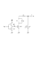
本実施の形態の半導体装置は、第1のトランジスタMP1、第2のトランジスタMN1、第3のトランジスタMD1、及びアンチヒューズ素子11を有するメモリ部10、端子A、及びESD保護素子EPを有する。ここでは、アンチヒューズ素子に情報が書き込まれる前のため、アンチヒューズ素子11は、容量Caで表す。
The semiconductor device according to the present embodiment includes a first transistor MP1, a second transistor MN1, a third transistor MD1, a
第1のトランジスタはP型トランジスタであり、第2のトランジスタはN型トランジスタであり、第1のトランジスタMP1及び第2のトランジスタMN1のゲートには制御信号Sigが入力されるよう構成されている。また、第1のトランジスタMP1の第1の端子TP1はロジック電源電圧VDDに配線され、第2の端子TP2は、第2のトランジスタMN1の第1の端子TN1及び第3のトランジスタMD1のゲートに接続されている。第2のトランジスタMN1の第2の端子TN2は、グランド配線GNDに接続されている。 The first transistor is a P-type transistor, the second transistor is an N-type transistor, and the control signal Sig is input to the gates of the first transistor MP1 and the second transistor MN1. The first terminal T P1 of the first transistor MP1 is wired to the logic power supply voltage VDD, a second terminal T P2 is the first terminal T N1 and the third transistor MD1 of the second transistor MN1 Connected to the gate. The second terminal T N2 of the second transistor MN1 is connected to the ground line GND.
第3のトランジスタMD1は、高耐圧トランジスタであり、アンチヒューズ素子11への電圧の印加を制御する。第3のトランジスタMD1の第1の端子TD1はアンチヒューズ素子11の第1の端子T111に接続され、第3のトランジスタMD1の第2の端子TD2はグランド配線GNDに接続されている。アンチヒューズ素子11の第2の端子T112は、抵抗素子Rsの第1の端子TS1に接続されている。ここで高耐圧トランジスタとは、制御部等の一般のロジック回路のトランジスタでは耐えられないような大きな電圧が印加されても故障しないよう形成されているトランジスタのことを指す。
The third transistor MD1 is a high breakdown voltage transistor and controls application of a voltage to the
端子Aは、メモリ部10と外部の素子を電気的に接続するためのパッドであり、アンチヒューズ素子11に電圧を印加するための端子である。また、端子Aは、ノードBでESD保護素子EPの第1の端子TEP1と接続され、ESD保護素子EPの第2の端子TEP2はグランド配線GNDに接続されている。アンチヒューズ素子11とノードBの間の電流経路には抵抗素子Rsが設けられており、抵抗素子Rsの第1の端子TS1は、アンチヒューズ素子11の第2の端子T112と接続され、抵抗素子Rsの第2の端子TS2はノードBに接続されている。
The terminal A is a pad for electrically connecting the
アンチヒューズ素子をメモリとして用いている半導体装置では、アンチヒューズ素子の導通、非導通により情報を記録している。このような半導体装置において、静電気放電(ESD:Electro−Static Discharge)により、非常に大きなサージ電流が端子Aから半導体装置内に侵入することがある。その場合、アンチヒューズ素子11が導通し、アンチヒューズ素子11を用いて半導体装置に記録されている情報が変化してしまうことがある。
In a semiconductor device using an antifuse element as a memory, information is recorded by conduction or non-conduction of the antifuse element. In such a semiconductor device, a very large surge current may intrude into the semiconductor device from the terminal A due to electrostatic discharge (ESD: Electro-Static Discharge). In that case, the
すなわち、ESDにより、通常の書き込み電圧や読み出し電圧に比べて非常に大きいサージ電圧がアンチヒューズ素子11に印加されるため、導通させる予定でなかったアンチヒューズ素子11が導通しすることがある。これにより、半導体装置に記録されている情報が変化してしまうことがある。
That is, ESD causes a surge voltage, which is much larger than normal write voltage and read voltage, to be applied to the
そこで、ESD保護素子EPを端子Aとアンチヒューズ素子11の間に設け、ESD対策を行う。この時、端子AとESD保護装置EPが接続されるノードBと、アンチヒューズ素子11との間に、抵抗素子Rsを設けると、抵抗素子Rsにより端子Aとアンチヒューズ素子11との間の電流経路に電流が流れにくくなる。これにより、大電流であるサージ電流がESD保護素子に流れやすくなり、より効果的にアンチヒューズ素子をESDのサージ電流から保護することができる。
Therefore, an ESD protection element EP is provided between the terminal A and the
一方、アンチヒューズ素子11に書き込みを行うために高電圧VHが印加される場合や、情報読みだしのためアンチヒューズ素子11の導通、非導通を検出する場合は、抵抗素子Rsの影響が小さい方が好ましい。
On the other hand, when the high voltage VH is applied to write to the
そこで、抵抗素子Rsとしては、抵抗値が電圧依存性を有し、抵抗素子Rsにかかる電圧が大きくなると抵抗の値が大きくなる抵抗素子を用いることが好ましい。このような抵抗素子を用いることで、アンチヒューズ素子11への書き込みや読み出しなどの通常動作の時よりも、ESDによるサージ電圧が半導体装置1に印加されたときの方が、抵抗素子Rsの抵抗値が大きくなる。
Therefore, as the resistance element Rs, it is preferable to use a resistance element whose resistance value is voltage-dependent and whose resistance value increases as the voltage applied to the resistance element Rs increases. By using such a resistance element, the resistance of the resistance element Rs is greater when a surge voltage due to ESD is applied to the
これにより、サージ電流により通常動作時より著しく大きい電流が半導体装置に流れる場合には、抵抗素子Rsの抵抗が大きくなる。すなわち、端子Aからアンチヒューズ素子11へより電流が流れにくくなる。よって、通常動作時に比べ、アンチヒューズ素子11への電流の侵入をより防ぐことができ、ESD保護素子EPにより多くの電流が流れる。
As a result, the resistance of the resistance element Rs increases when a current that is significantly larger than that during normal operation flows through the semiconductor device due to a surge current. That is, the current is less likely to flow from the terminal A to the
一方、通常動作時の電圧下では、サージ電圧印加時よりも抵抗素子Rsの抵抗値は小さい。よって、端子Aとアンチヒューズ素子11との間の電流経路に電流が流れやすくなり、抵抗素子Rsによるアンチヒューズ素子11への書き込みや読み込み動作に対する影響は小さくなる。
On the other hand, under the voltage during normal operation, the resistance value of the resistance element Rs is smaller than when the surge voltage is applied. Therefore, current easily flows through the current path between the terminal A and the
したがって、通常動作時のアンチヒューズ素子11への書き込みや読み出しの阻害を低減しつつ、アンチヒューズ素子11に記録された情報を効果的に保護することができる。半導体装置の具体的な構成を、図1を参照して説明する。第1のトランジスタMP1は、例えば低耐圧ロジック回路を構成するPMOSトランジスタ、第2のトランジスタMN1は、低耐圧ロジック回路を構成するNMOSトランジスタとすることができる。
Therefore, it is possible to effectively protect the information recorded in the
ここで、低耐圧ロジック回路とは、構成する第1のトランジスタMP1及び第2のトランジスタMN1の耐圧が、高耐圧トランジスタMD1より低いトランジスタであるロジック回路であり、通常のロジック回路に比べて耐圧が低いものではない。第1のトランジスタMP1のソースとバックゲートはロジック電源電圧VDDに接続されており、第2のトランジスタのMN1のソースとバックゲートはGNDに接続されている。上述のように、第1のトランジスタMP1のゲートと第2のトランジスタMN1のゲートには、制御信号Sigが入力されている。第1のトランジスタMP1のドレインと第2のトランジスタMN1のドレインは接続されており、第1のトランジスタMP1と第2のトランジスタMN1でインバータ回路を構成している。 Here, the low breakdown voltage logic circuit is a logic circuit in which the breakdown voltage of the first transistor MP1 and the second transistor MN1 constituting the transistor is lower than that of the high breakdown voltage transistor MD1, and the breakdown voltage is higher than that of a normal logic circuit. Not low. The source and back gate of the first transistor MP1 are connected to the logic power supply voltage VDD, and the source and back gate of the second transistor MN1 are connected to GND. As described above, the control signal Sig is input to the gate of the first transistor MP1 and the gate of the second transistor MN1. The drain of the first transistor MP1 and the drain of the second transistor MN1 are connected, and the first transistor MP1 and the second transistor MN1 constitute an inverter circuit.
該インバータ回路の出力信号Vgは、アンチヒューズ素子11への書込みを制御する第3のトランジスタMD1のゲートに入力されている。ここで、第3のトランジスタMD1は、例えば、高耐圧NMOSトランジスタとすることができる。第3のトランジスタMD1のソースおよびバックゲートはGNDに接続されており、ドレインはアンチヒューズ素子である容量Caの第1の端子に接続されている。容量Caの第2の端子は抵抗素子Rsの第1の端子に接続される。抵抗素子Rsの第2の端子は、端子Aに接続され、端子Aには情報書込み時に印加する高電圧VHが供給される。抵抗Rsと端子Aの間にはESD保護素子EPであるダイオードのカソード側が接続され、アノード側は接地される。
The output signal Vg of the inverter circuit is input to the gate of the third transistor MD1 that controls writing to the
ESD保護素子EPは、このダイオードのブレイクダウン電圧が情報書き込み時に端子Aに印加される電圧VHよりも高くなるように構成されている。 The ESD protection element EP is configured such that the breakdown voltage of the diode is higher than the voltage VH applied to the terminal A when information is written.
次に、図2に図1で示す点線で囲んだ部分の断面構造を示す。 Next, FIG. 2 shows a cross-sectional structure of a portion surrounded by a dotted line shown in FIG.
P型シリコン基板100上に、Pウエル領域101とNウエル領域102a、102bが形成されている。Pウエル領域101は、低耐圧ロジック回路を構成するNMOSトランジスタのPウエルと同じ工程で形成することができる。また、Nウエル領域102a、102bは、低耐圧ロジック回路を構成するPMOSトランジスタのNウエルと同じ工程で形成することができる。
なお、P型シリコン基板100に対するNウエル領域の不純物濃度は、Nウエル領域102a、102bとP型シリコン基板100とのブレイクダウン電圧が、高電圧VHより高くなる濃度となっている。また、Pウエル領域101とNウエル領域102a、102bの不純物濃度は、Pウエル領域101とNウエル領域102a、102bとのブレイクダウン電圧が、高電圧VHより高くなる濃度となっている。
The impurity concentration in the N well region with respect to the P
Pウエル領域101及びNウエル領域102a、102bに、LOCOS構造を有するフィールド酸化膜103、高濃度N型拡散領域106a〜106c、及び高濃度P型拡散領域107が形成されている。
In the
高耐圧NMOSトランジスタである第3のトランジスタMD1の構成を説明する。ゲート電極105aは、ゲート酸化膜104を介して、隣接するPウエル領域101とNウエル領域102aの上に配置される。Pウエル領域101とゲート電極105aの重なる領域がチャネル領域となる。
A configuration of the third transistor MD1 which is a high voltage NMOS transistor will be described.
高濃度のN型拡散領域106aは第3のトランジスタMD1のソース電極であって、高濃度P型拡散領域107はバックゲート電極である。Nウェル領域102aは、ドレインの電界緩和領域として、ゲート電極105aの下部まで延在している部分を有する。Nウエル領域102a内に形成された高濃度N型拡散領域106bが、第3のトランジスタMD1のドレイン電極となる。更に、ゲート電極105aのドレイン側は、Nウエル102内に形成されたフィールド酸化膜103上に乗り上げた構造、所謂、LOCOSオフセット構造を有している。
The high concentration N
これにより、第3のトランジスタMD1がOFF状態、すなわち、ゲート電極の電圧がGNDで、ドレイン電極の電圧が高電圧VHまで上昇しても、ゲート−ドレイン耐圧が確保できる。 Thereby, even if the third transistor MD1 is in the OFF state, that is, the voltage of the gate electrode is GND and the voltage of the drain electrode rises to the high voltage VH, the gate-drain breakdown voltage can be ensured.
次に、アンチヒューズ素子11の構造を説明する。アンチヒューズ素子11は、上部電極(第1の電極)、下部電極(第2の電極)、及びその間の絶縁層を有する。たとえば、Nウエル領域102bの上にゲート酸化膜104を介して設けられた電極105bが、アンチヒューズ素子11の上部電極(第1の電極)として機能する。また、Nウェル領域102bにおいて、高濃度N型拡散領域106cに接続され、平面視で上部電極と重複する部分が、下部電極(第2の電極)として機能する。
Next, the structure of the
図2では、Nウェル領域102bの、平面視において上部電極と重ならない領域のみに高濃度N型拡散領域106cが形成されているが、高濃度N型拡散領域106cはこれに限定されない。例えば、上部電極と重複する部分の一部、または重複する部分全域に高濃度N型拡散領域106bが形成されている工程としてもよい。平面視において上部電極と重なる領域に高濃度N型拡散領域106cも形成されている場合には、高濃度N型拡散領域106cの重複部分もアンチヒューズ素子11の下部電極として機能する。
In FIG. 2, the high-concentration N-
さらに、図2では、アンチヒューズ素子11の下部電極が第3のトランジスタMD1のドレインに接続されているが、上部電極が第3の第3のトランジスタMD1のドレインに接続され、下部電極が高電圧VHに接続されていてもよい。
Further, in FIG. 2, the lower electrode of the
ゲート酸化膜104は、低耐圧ロジック回路を構成する第1及び第2のトランジスタMP1及びMN1のゲート酸化膜の形成工程で形成することができる。また、電極105a、105bは、例えばポリシリコン層とすることができる。ポリシリコン層、高濃度N型拡散領域106a〜106c、及び、高濃度P型拡散領域107は、低耐圧ロジック回路を構成する第1及び第2のトランジスタMP1及びMN1の、各要素の形成工程と同じ工程で形成することができる。
The
このように、アンチヒューズ素子11をMOS構造を有するアンチヒューズ素子とし、アンチヒューズ素子への書き込みを制御するトラジスタをMOSトランジスタとすることで、アンチヒューズ素子とトランジスタを同じ工程で形成することができる。このため、少ない工程数で安価に半導体装置を形成することができる。
As described above, the
高濃度P型拡散領域107、N型拡散領域106a〜106c、及びフィールド酸化膜103上には複数のコンタクト部108が設けられた絶縁膜が設けられ、絶縁膜上には、金属配線109a〜109dが設けられている。なお、金属配線109a〜109dと各電極は、電気的に接続されていれば、その製造手法および構造は限定されない。
An insulating film having a plurality of
図2では、アンチヒューズ素子11として、下部電極及び上部電極がNウエル領域とポリシリコンで形成される容量を例として示しているが、アンチヒューズ素子11はこの構造に限定されず、例えばPMOSトランジスタを用いた容量であってもよい。
In FIG. 2, as the
次に、各電極の接続状態を説明する。 Next, the connection state of each electrode will be described.
金属配線109aは、コンタクト部108を介して第3のトランジスタMD1のソース電極とバックゲート電極に接続されており、GND電位が与えられる。金属配線109bは、コンタクト部108を介して第3のトランジスタMD1のゲート電極105aに接続され、図1に示すインバータ回路の出力信号Vgが入力される。金属配線109cは、コンタクト部108を介して第3のトランジスタMD1のドレイン電極とアンチヒューズ素子11の下部電極に接続されている。金属配線109dは、コンタクト部108を介してアンチヒューズ素子11の上部電極に接続され、書込み時の高電圧VHが与えられる。
The
次に、書込み時の動作を説明する。 Next, the operation at the time of writing will be described.
アンチヒューズ素子11に情報を書込みたいときは、制御信号SigにLoレベルの信号を入力することにより、高耐圧NMOSトランジスタである第3のトランジスタMD1をON状態にする。これにより、アンチヒューズ素子11を構成する上部電極及び下部電極の2つの電極に、高電圧VHが印加される。したがって、2つの電極の間のゲート酸化膜104が絶縁破壊され、アンチヒューズ素子11に情報が書込まれる。即ち書き込み前はアンチヒューズ素子11は容量素子であったのに対し、書き込み後は抵抗素子となる。
When information is to be written to the
よって、アンチヒューズ素子に書込まれた情報を読出す方法としては、例えば、アンチヒューズ素子のインピーダンスの変化を測定する方法がある。 Therefore, as a method of reading information written in the antifuse element, for example, there is a method of measuring a change in impedance of the antifuse element.
アンチヒューズ素子に記録する情報は、チップIDや設定パラメータ等の製品固有情報であり、これらは、例えば製品出荷時に工場にて検査機等を用いて書込みが行われる。或は、製品本体に搭載され、ユーザが製品の使用開始後に情報を書込む場合は、製品本体から高電圧VHに相当する電圧が供給される。 The information recorded in the antifuse element is product-specific information such as a chip ID and setting parameters, and these are written using a testing machine or the like at the time of product shipment. Alternatively, when the information is mounted on the product body and the user writes information after the use of the product is started, a voltage corresponding to the high voltage VH is supplied from the product body.
一方、製品製造工程やユーザが使用する際に静電気放電(ESD:Electro−Static Discharge)により非常に大きなサージ電流が端子Aから半導体装置内に侵入する可能性がある。このような非常に大きなサージ電流が半導体装置内の、例えばアンチヒューズ素子11に侵入すると、アンチヒューズ素子11が導通し、記録されている情報が変化することがある。
On the other hand, when a product is used or used by a user, a very large surge current may enter the semiconductor device from the terminal A due to electrostatic discharge (ESD). When such a very large surge current enters, for example, the
本実施の形態では、抵抗素子Rsを、端子AとESD保護素子EPが接続するノードとアンチヒューズ素子11との間に設けることで、端子Aに侵入したサージ電流をESD保護素子EPにより逃がすことができる。よって、アンチヒューズ素子11となる容量Caに流れ込むのを防ぐことが可能となる。これにより、アンチヒューズ素子となる容量Caに書き込まれている情報が、静電気放電等により変化するのを防ぐことができる。
In the present embodiment, the resistance element Rs is provided between the node connected to the terminal A and the ESD protection element EP and the
さらに、抵抗素子Rsを、抵抗値が電圧依存性を有し、抵抗素子Rsにかかる電圧が大きくなると抵抗値も大きくなる抵抗とすることで、通常動作の阻害を低減し、より効果的にESD対策を行うことができる。 Furthermore, the resistance element Rs is a resistance whose resistance value is voltage-dependent, and the resistance value increases as the voltage applied to the resistance element Rs increases, so that the inhibition of normal operation is reduced and ESD is more effectively performed. Measures can be taken.
(第2の実施の形態)
第1の実施の形態で示した静電気放電(ESD:Electro−Static Discharge)による高いサージに対する耐性をより向上させる例を示す。半導体装置の回路構成は図1と同じである。
(Second Embodiment)
An example is shown in which resistance to high surges caused by electrostatic discharge (ESD) shown in the first embodiment is further improved. The circuit configuration of the semiconductor device is the same as that in FIG.
ESDによる高いサージ電圧によるアンチヒューズ素子11の破壊を防ぐためには、アンチヒューズ素子11よりもESD保護素子EPに優先的にサージ電流が流れる構成であることが好ましいため、抵抗素子Rsの抵抗値は高い方が好ましい。一方、抵抗素子Rsの抵抗値が高いと通常の書き込み動作においては、アンチヒューズ素子11のゲート酸化膜破壊の安定性が損なわれる。さらに、読出しの際には書き込み後のアンチヒューズの抵抗成分以外の抵抗成分は少ない方が好ましい。
In order to prevent destruction of the
したがって、抵抗素子Rsとしては、アンチヒューズ素子11への書き込みや読み出し等の通常動作時には抵抗値が小さく、ESDによるサージ電圧等の通常駆動時の電圧範囲を大きく超える電圧が印加される場合には抵抗地が大きくなる抵抗素子が好ましい。さらに、抵抗素子Rsとして、印加される電圧が大きくなった場合に、抵抗値が単調増加し、かつその増加率も単調増加するような抵抗素子とすると、半導体装置としての通常動作の抑制をより低減しつつ、ESD保護素子をより有効に機能させることができる。
Therefore, the resistance element Rs has a small resistance value during normal operation such as writing to and reading from the
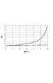
図3に本実施の形態における抵抗素子Rsの一例の平面図を示す。本実施形態の抵抗素子Rsは拡散抵抗でありP型シリコン基板201中にN型拡散抵抗領域202を作製している。抵抗素子Rsは、N型拡散抵抗領域202に加え、第1の接続領域203及び第2の接続領域204を有する。図4は図3の破線に沿った抵抗素子Rsの断面構造を示すものである。この構造では、N型拡散抵抗領域202にかかる電圧の大きさによって抵抗値が変化する。これは、N型拡散抵抗領域202とP型シリコン基板201の接合部に生ずる空乏層領域が変化することで空乏層領域の幅も変化し、実質的な抵抗幅が変化することに起因する。高電圧が印加されると、実質的な抵抗幅は狭くなる。
FIG. 3 shows a plan view of an example of the resistance element Rs in the present embodiment. The resistance element Rs of this embodiment is a diffused resistor, and an N-type diffused
図5にN型拡散抵抗領域202にかかる電圧と抵抗素子Rsの抵抗値を示す。図5は電圧0Vの抵抗値で規格化したものである。本実施の形態ではアンチヒューズ素子11に書き込みする際の端子Aに印加する印加電圧を20Vとする。図5に示すように、大きなサージ電流が侵入した場合、抵抗素子Rs自身により電圧が上昇し、それにより抵抗素子Rsの抵抗値が、上昇する。ここでは、抵抗素子Rsは、印加される電圧が大きくなると、抵抗値が単調増加し、また、その増加率も単調増加している。
FIG. 5 shows the voltage applied to the N-type
したがって、通常の書き込み動作時及び読み出し動作時には、抵抗素子Rsの抵抗は小さく、書き込み動作の安定性や読み出し動作への影響を小さいものとできる。加えて、ESD等によりサージ電圧が発生した際には、抵抗素子Rsの抵抗が単調増加し、その変化率も単調増加するため、サージ電流はアンチヒューズ素子11よりも保護素子EPに優先的に流れる。
Accordingly, during normal write operation and read operation, the resistance of the resistance element Rs is small, and the stability of the write operation and the influence on the read operation can be reduced. In addition, when a surge voltage is generated due to ESD or the like, the resistance of the resistance element Rs monotonously increases and the rate of change also monotonously increases. Therefore, the surge current is given priority to the protection element EP over the
よって、サージ電圧発生時、アンチヒューズ素子11がサージ電流により破壊されるのを低減することができる。つまり、抵抗素子Rsを本実施の形態に記載の抵抗素子Rsとすることで、抵抗が一定の抵抗等を抵抗素子Rsとして用いる場合に比べ、アンチヒューズ素子のサージに対する耐性を、より向上することができる。
Therefore, when the surge voltage is generated, it is possible to reduce the destruction of the
以上より、本実施の形態で説明した抵抗素子を抵抗素子Rsとして用いることで、半導体装置1の通常の書き込みや読み出し動作を、より安定的に効率化して行うことができ、かつ、ESD保護素子による半導体装置1の保護を、より確実に行うことができる。
As described above, by using the resistance element described in this embodiment as the resistance element Rs, normal writing and reading operations of the
(第3の実施の形態)
第2の実施の形態で示した静電気放電(ESD:Electro−Static Discharge)による高いサージに対する耐性をより向上させる例を示す。半導体装置1の一例の回路構成を図6に示す。
(Third embodiment)
An example of further improving the resistance against a high surge caused by electrostatic discharge (ESD) shown in the second embodiment will be described. A circuit configuration of an example of the
図6に示すように本実施の形態では、抵抗素子Rs(第1の抵抗素子)に加え、アンチヒューズ素子11と並列に抵抗素子Rp(第2の抵抗素子)が配置されている。高耐圧NMOSトランジスタMD1がオフ状態にある場合、抵抗素子Rpはアンチヒューズ素子11である容量Caの両端の電位を揃える効果があり、これによりサージに対する耐性をより向上させる。この両端電位を揃える効果は抵抗素子Rpの抵抗値が低い方がよい。本実施の形態では抵抗素子RsおよびRpは、例えば拡散抵抗で構成することができ、構造は図3および4で示したものを用いることができる。一方で、抵抗素子Rsの幅Wrsと抵抗素子Rpの幅Wrpの関係は次式の通りである。
Wrs<Wrp (式1)
As shown in FIG. 6, in the present embodiment, in addition to the resistance element Rs (first resistance element), a resistance element Rp (second resistance element) is arranged in parallel with the
Wrs <Wrp (Formula 1)
ここで、抵抗素子Rsの幅Wrsは、抵抗素子Rsにおいて抵抗素子として機能する領域の、電流経路に対して垂直な方向における長さである。また、抵抗素子Wppの幅Wrpは、抵抗素子Rpにおいて、抵抗素子として機能する領域の、電流経路に対して垂直な方向における長さである。 Here, the width Wrs of the resistance element Rs is a length in a direction perpendicular to the current path of a region functioning as the resistance element in the resistance element Rs. Further, the width Wrp of the resistance element Wpp is the length in the direction perpendicular to the current path of the region functioning as the resistance element in the resistance element Rp.
抵抗素子Rsの幅を抵抗素子Rpよりも狭くすることで、抵抗素子Rsの方が抵抗の電圧依存度が高くなる。図7に規格化したN型拡散抵抗領域202にかかる電圧と抵抗素子RsおよびRpの抵抗値を示す。実線が抵抗素子Rsの抵抗値、破線が抵抗素子Rpの抵抗値を示している。式1の関係となるように抵抗幅Wを調整することで抵抗素子RsとTpの電圧依存度に差をつけることが可能となる。本実施の形態ではアンチヒューズ素子11に書き込みする際の端子Aに印加する印加電圧を20Vとする。
By making the width of the resistive element Rs narrower than that of the resistive element Rp, the resistive element Rs has a higher voltage dependency of the resistance. FIG. 7 shows the voltage applied to the normalized N-type
抵抗素子Rsは、書き込み電圧より高い電圧が印加される状態になると、書き込み電圧印加時より抵抗値が高くなるため、サージに対する耐性を向上させることができる。さらに抵抗素子Rpは、書き込み電圧以上の電圧が印加されても抵抗値の上昇は少ない。そのためアンチヒューズ素子11である容量Caの両端電位を揃える効果が保たれ、サージに対する耐性をより向上させることができる。また、抵抗素子RsとRpを同一の構造とすることでプロセスコストの増加を防ぐことが可能となる。
When the resistance element Rs is in a state where a voltage higher than the write voltage is applied, the resistance value becomes higher than when the write voltage is applied, and thus the resistance against the surge can be improved. Furthermore, the resistance value of the resistance element Rp is small even when a voltage higher than the write voltage is applied. Therefore, the effect of aligning the potentials at both ends of the capacitor Ca that is the
図6に示すESD保護素子EPは、高耐圧MOSトランジスタとすることができ、例えば高耐圧NMOSトランジスタとすることができる。ESD保護素子EPである高耐圧NMOSトランジスタのゲートとソースとバックゲートは接地され、ドレインが端子Aと抵抗素子Rsの間に接続されている。これにより高耐圧NMOSトランジスタのブレイクダウンとスナップバック動作を利用して、ダイオードよりも多くの電流を逃がすことが可能となる。ESD保護素子として高耐圧NMOSトランジスタMD1と同じ構造を用いることで、プロセスコストの増加を防ぐことができる。 The ESD protection element EP shown in FIG. 6 can be a high voltage MOS transistor, for example, a high voltage NMOS transistor. The gate, source, and back gate of the high-breakdown-voltage NMOS transistor that is the ESD protection element EP are grounded, and the drain is connected between the terminal A and the resistance element Rs. This makes it possible to release more current than the diode using the breakdown and snapback operations of the high voltage NMOS transistor. By using the same structure as the high breakdown voltage NMOS transistor MD1 as the ESD protection element, an increase in process cost can be prevented.
(第4の実施の形態)
本実施の形態では、実施の形態1乃至3のいずれか1つに記載の半導体装置1の適用例として、半導体装置1を記録装置に適用した例について説明する。
(Fourth embodiment)
In this embodiment, an example in which the
図8は、実施の形態1乃至3のいずれかに記載の半導体装置1を有する記録ヘッド用基板の回路構成の一例を示す。記録ヘッド用基板は、メモリユニット302及び論理回路NAND回路と、記録ユニット301を有する。
FIG. 8 shows an example of a circuit configuration of a recording head substrate having the
メモリユニット302は、第1のトランジスタMP1及び第2のトランジスタMN1からなるインバータ、第3のトランジスタMD1、アンチヒューズ素子11、抵抗素子Rs、ノードB、及びESD保護素子EPを有する。また、記録ユニット301は、ヒータRh(電気熱変換素子)と、ヒータRhを駆動する駆動部(例えば、トランジスタMD2及び論理積回路AND)と、を有する。ヒータRhを駆動することにより、即ち、ヒータRhを通電させて熱を発生させることにより、記録剤が吐出され、記録を行うことが可能である。
The
制御回路303は、例えば、不図示のシフトレジスタやラッチ回路等によって構成することができる。制御回路303には、例えば、不図示のホストPC等を介して、クロック信号CLK、画像データ信号DATA、ラッチ信号LT、ヒータ制御信号HEが入力されてもよい。また、論理積回路AND及びNAND、並びに制御回路303には、ロジック用の電源電圧として、第1の電源電圧VDD(例えば、3〜5V)が供給される。よって、記録ユニット301のヒータRhとメモリユニット302(半導体装置)は、それぞれ制御回路303に電気的に接続されている。
The
ここで、制御回路303は、例えば、其々がn個の記録ユニット301を有するm個のグループについて、グループごとに記録ユニット301の動作を制御してヒータRhを駆動する時分割駆動を為しうる。時分割駆動は、制御回路303が、mビットのブロック選択信号304と、nビットの時分割選択信号305とを出力して為されうる。
Here, for example, for the m groups each having
論理積回路ANDには、対応するブロック選択信号304及び時分割選択信号305が入力され、それに応答してトランジスタMD2を導通状態にし、トランジスタMD2と直列に接続されたヒータRhを駆動する。ここで、記録ユニット301には、ヒータ駆動用の電源電圧として第2の電源電圧VH1(例えば、24V)が供給され、接地電位をGNDとする。
Corresponding
論理積回路NANDには、制御信号306及び時分割選択信号305が入力され、それに応じた信号がインバータからトランジスタMD1に出力され、トランジスタMD1の導通状態/非導通状態が切り替えられる。半導体装置1には、アンチヒューズ素子11に情報を書き込むための第3の電源電圧VH2が供給され、接地電位をGNDとする。
A
なお、図8では、メモリユニット302毎にESD保護素子EPを配置する構成としたが、図9に示すように、VH2端子と接地端子との間に少なくとも1つのESD保護素子を配置する構成としてもよい。この場合、メモリユニットは、ESD保護素子EPを有さず、例えば、インバータ、第3のトランジスタMD1、アンチヒューズ素子11、及び抵抗素子Rsを有する。
In FIG. 8, the ESD protection element EP is arranged for each
また、図8及び9では、記録ユニット301とメモリユニット302が、ともに制御回路303に接続されている構成を示したが、それぞれ、別の制御回路に接続される構成であってもよい。
8 and 9, the
図10乃至12を参照しながら、上記記録ヘッド用基板を記録装置に搭載した例について、インクジェット記録方式のものを例示して説明する。しかし、記録装置はこの形態には限定されず、例えば、溶融型や昇華型等の熱転写方式の記録装置についても同様である。記録装置は、例えば、記録機能のみを有するシングルファンクションプリンタであっても良いし、例えば、記録機能、FAX機能、スキャナ機能等の複数の機能を有するマルチファンクションプリンタであっても良い。また、記録装置は、例えば、カラーフィルタ、電子デバイス、光学デバイス、微小構造物等を所定の記録方式で製造するための製造装置であっても良い。 An example in which the recording head substrate is mounted on a recording apparatus will be described with reference to FIGS. However, the recording apparatus is not limited to this form, and the same applies to, for example, a thermal transfer type recording apparatus such as a melt type or a sublimation type. The recording device may be, for example, a single function printer having only a recording function, or may be, for example, a multi-function printer having a plurality of functions such as a recording function, a FAX function, and a scanner function. Further, the recording apparatus may be a manufacturing apparatus for manufacturing a color filter, an electronic device, an optical device, a minute structure, and the like by a predetermined recording method, for example.
「記録」は、記録媒体上に画像、模様、パターン、構造物等、人間が視覚で知覚し得るように顕在化したものを形成する場合だけでなく、媒体の加工を行う場合をも含みうる。「記録媒体」とは、一般的な記録装置で用いられる紙のみならず、布、プラスチック・フィルム、金属板、ガラス、セラミックス、樹脂、木材、皮革等、記録剤を付することが可能なものをも含みうる。「記録剤」は、記録媒体に付されることにより、画像、模様、パターン等の形成又は記録媒体の加工に供されうるインク等の液体だけでなく、記録剤の処理(例えば、記録剤が含有する色剤の凝固又は不溶化)に供されうる液体をも含みうる。 “Recording” may include not only the formation of images, patterns, patterns, structures, etc. that are visible so that humans can perceive them visually, but also the processing of media. . "Recording medium" means not only paper used in general recording equipment but also cloth, plastic film, metal plate, glass, ceramics, resin, wood, leather, etc., to which a recording agent can be applied. May also be included. The “recording agent” is applied to the recording medium, whereby not only a liquid such as an ink that can be used for forming an image, a pattern, a pattern, or the like or processing of the recording medium, but also a treatment of the recording agent (for example, a recording agent It may also include a liquid that can be used for coagulation or insolubilization of the contained colorant.
図10は、本実施の形態のインクジェット記録方式の記録ヘッド用の基板152及びインク供給部の構成例の一部を模式的に示している。記録ヘッド用の基板152は、インクを吐出するための各ノズル153(吐出口)に対応して配列された複数のヒータ141(電気熱変換素子)を有する。ヒータ141を駆動することによってインクを加熱し、発泡させ、ノズル153からインクを吐出する。記録ヘッド用基板152には、例えば図8を用いて説明した記録ヘッド用基板を用いることができる。
FIG. 10 schematically shows a part of a configuration example of the
電極154は、ヒータ141を通電させるための電極であり、例えば、ヒータ141を駆動する駆動素子に電気的に接続されうる。各ノズル153は、吐出するためのインクが供給されるように、対応するインクの流路155を介して、共通液室157に連結されている。部材156は、これらノズル153、流路155、共通液室157を形成するように内部に溝を有する。
The
なお、ここでは例として、ヒータ141を用いて加熱することでインクを吐出する記録ヘッド用の基板の例を示したが、本発明の記録ヘッド用の基板は、これに限定されない。例えば、吐出用素子としてヒータ141の代わりにピエゾ素子を用いた構成としてもよい。
Note that, here, as an example, an example of a substrate for a recording head that discharges ink by heating using the
図11は、記録ヘッド810の外観を例示している。記録ヘッド810は、複数のノズル153及び複数のノズル153と対向した設けられた記録ヘッド用基板152を有する記録ヘッド部811と、記録ヘッド部811に取り付けられたインクタンク812を備えうる。インクタンク812は、記録ヘッド部811に供給するためのインクを保持する。インクタンク812と記録ヘッド部811とは、例えば破線Kで分離することができ、インクタンク812を交換することができる。
FIG. 11 illustrates the appearance of the
記録ヘッド810は、キャリッジ920(図12)からの電気信号を受け取るための電気的コンタクト(不図示)を備えており、当該電気信号にしたがってインクを吐出して上述の記録を行う。インクタンク812は、例えば繊維質状又は多孔質状のインク保持材(不図示)を有しており、当該インク保持材によってインクを保持しうる。
The
図12は、記録装置900の鳥瞰図を示している。記録ヘッド810は、図11に一部を示した記録ヘッドであり、インクタンク(記録剤容器)と共に、キャリッジ920の上に搭載されうる。キャリッジ920は、螺旋溝921を有するリードスクリュー904に取り付けられうる。リードスクリュー904の回転により、記録ヘッド810は、キャリッジ920と共にガイド919に沿って矢印a又はb方向に移動しうる。リードスクリュー904の回転は、駆動力伝達ギア902及び903を介して、駆動モータ901の回転に連動する。
FIG. 12 shows a bird's eye view of the
記録用紙Pは、搬送部(不図示)によってプラテン906の上に搬送されうる。紙押え板905は、キャリッジ移動方向に沿って、記録用紙Pをプラテン906に対して押えうる。記録装置900は、フォトカプラ907及び908を介して、キャリッジ920に設けられたレバー909の位置を確認し、駆動モータ901の回転方向の切換等を行いうる。支持部材910は、記録ヘッド810の各ノズルをキャッピングするキャップ部材911を支持しうる。吸引手段912は、キャップ部材911の内部を吸引し、キャップ内開口913を介して記録ヘッド810の吸引回復処理を為しうる。
The recording paper P can be transported onto the
クリーニングブレード914には、周知のクリーニングブレードが用いられ、移動部材915がクリーニングブレード914を前後方向に移動させうる。本体支持板916は、移動部材915及びクリーニングブレード914を支持しうる。レバー917は、吸引回復処理を開始するために設けられうる。
A known cleaning blade is used as the
キャリッジ920と係合するカム918の移動に伴って、レバー917が移動する。駆動モータ901からの駆動力はクラッチ切換等の公知の伝達手段によって制御されうる。記録装置900には記録制御部(不図示)が設けられ、記録装置900は、外部からの記録データ等の電気信号に従って、各機構のそれぞれの駆動を制御しうる。記録装置900は、記録ヘッド810の往復移動と、搬送部(不図示)による記録用紙Pの搬送とを繰り返し、記録用紙Pへの記録を完成させうる。
As the
また、上記記録装置は、3Dデータを有し、3次元の像を形成する装置としても用いることができる。 The recording device can also be used as a device having 3D data and forming a three-dimensional image.
このように、実施の形態1乃至3のいずれかの半導体装置1を記録装置に適用することによって、アンチヒューズメモリの情報がESDによって変化するのを防ぐことができ、記録装置の信頼性を向上することができる。
As described above, by applying the
1 半導体装置
11 アンチヒューズ素子
MD1 第3のトランジスタ(高耐圧トランジスタ)
EP ESD保護素子
B ノード
Rs 第1の抵抗素子
Rp 第2高濃度N型拡散領域
DESCRIPTION OF
EP ESD protection element B node Rs First resistance element Rp Second high-concentration N-type diffusion region
Claims (19)
前記アンチヒューズ素子に電圧を印加するための端子と、
前記アンチヒューズ素子を介して前記端子に接続され、前記アンチヒューズ素子への電圧の印加を制御するトランジスタと、
前記端子と、ノードを介して接続されたESD(Electro−Static Discharge)保護素子と、
前記ノードと前記アンチヒューズ素子との間の電流経路に設けられた第1の抵抗素子と、
前記アンチヒューズ素子と並列に接続された第2の抵抗素子と、
を有し、
前記第1の抵抗素子に印加される電圧が大きくなると、前記第1の抵抗素子の抵抗値は大きくなり、
前記アンチヒューズ素子に情報を書き込む際に前記端子に印加する電圧より高い電圧を印加した際の抵抗の変化率が、前記第2の抵抗素子より前記第1の抵抗素子の方が大きいことを特徴とする半導体装置。 An antifuse element;
A terminal for applying a voltage to the antifuse element;
A transistor connected to the terminal via the antifuse element and controlling application of a voltage to the antifuse element;
An ESD (Electro-Static Discharge) protection element connected via the node with the terminal;
A first resistance element provided in a current path between the node and the antifuse element;
A second resistance element connected in parallel with the antifuse element;
Have
If the voltage applied to the first resistance element increases, the resistance value of the first resistor element is greater Ri Na,
The rate of change in resistance when a voltage higher than the voltage applied to the terminal when writing information to the antifuse element is larger in the first resistance element than in the second resistance element. A semiconductor device.
ソースおよびドレインの一方が、前記アンチヒューズ素子の一端と接続され、ソースおよびドレインの他方に第1電位が供給されるトランジスタと、
前記アンチヒューズ素子の他端に一端が接続され、前記第1電位とは異なる第2電位が供給される端子に他端が接続された第1の抵抗素子と、
前記端子と、前記第1の抵抗素子の他端との間の電気経路に接続されたESD(Electro−Static Discharge)保護素子と、
前記アンチヒューズ素子と並列に接続された第2の抵抗素子と、
を有し、
前記第1の抵抗素子は拡散抵抗であり、
前記アンチヒューズ素子に情報を書き込む際に前記端子に印加する電圧より高い電圧を印加した際の抵抗の変化率が、前記第2の抵抗素子より前記第1の抵抗素子の方が大きいことを特徴とする半導体装置。 An antifuse element;
A transistor in which one of a source and a drain is connected to one end of the antifuse element, and a first potential is supplied to the other of the source and the drain;
A first resistance element having one end connected to the other end of the anti-fuse element and having the other end connected to a terminal to which a second potential different from the first potential is supplied;
An ESD (Electro-Static Discharge) protection element connected to an electrical path between the terminal and the other end of the first resistance element;
A second resistance element connected in parallel with the antifuse element;
Have
Said first resistive element Ri der diffusion resistance,
The rate of change in resistance when a voltage higher than the voltage applied to the terminal when writing information to the antifuse element is larger in the first resistance element than in the second resistance element. A semiconductor device.
前記記録ヘッド部に取り付けられたインクタンクと、
を有し、
前記記録ヘッド用基板は、
前記複数の吐出口に対応するように設けられた吐出用素子と、
前記吐出用素子と電気的に接続された制御回路と、
前記制御回路と電気的に接続された請求項1乃至17のいずれか1項に半導体装置と、を有することを特徴とする記録装置。 A recording head portion having a plurality of ejection openings and a recording head substrate;
An ink tank attached to the recording head unit;
Have
The recording head substrate is:
An ejection element provided to correspond to the plurality of ejection ports;
A control circuit electrically connected to the ejection element;
Recording apparatus comprising: the semiconductor device, to any one of the control circuit and electrically connected to the preceding claims 1 7.
Priority Applications (2)
| Application Number | Priority Date | Filing Date | Title |
|---|---|---|---|
| JP2015249092A JP6608269B2 (en) | 2015-12-21 | 2015-12-21 | Semiconductor device and recording device |
| US15/383,513 US9895879B2 (en) | 2015-12-21 | 2016-12-19 | Semiconductor device and recording device |
Applications Claiming Priority (1)
| Application Number | Priority Date | Filing Date | Title |
|---|---|---|---|
| JP2015249092A JP6608269B2 (en) | 2015-12-21 | 2015-12-21 | Semiconductor device and recording device |
Publications (3)
| Publication Number | Publication Date |
|---|---|
| JP2017117854A JP2017117854A (en) | 2017-06-29 |
| JP2017117854A5 JP2017117854A5 (en) | 2018-11-29 |
| JP6608269B2 true JP6608269B2 (en) | 2019-11-20 |
Family
ID=59065004
Family Applications (1)
| Application Number | Title | Priority Date | Filing Date |
|---|---|---|---|
| JP2015249092A Active JP6608269B2 (en) | 2015-12-21 | 2015-12-21 | Semiconductor device and recording device |
Country Status (2)
| Country | Link |
|---|---|
| US (1) | US9895879B2 (en) |
| JP (1) | JP6608269B2 (en) |
Families Citing this family (4)
| Publication number | Priority date | Publication date | Assignee | Title |
|---|---|---|---|---|
| DE102016111641A1 (en) * | 2016-06-24 | 2017-12-28 | Infineon Technologies Ag | switch |
| JP7173661B2 (en) | 2018-11-16 | 2022-11-16 | ミネベアミツミ株式会社 | Humidity detector |
| WO2020162919A1 (en) | 2019-02-06 | 2020-08-13 | Hewlett-Packard Development Company, L.P. | Communicating print component |
| US11529805B2 (en) | 2019-02-06 | 2022-12-20 | Hewlett-Packard Development Company, L.P. | Communicating print component |
Family Cites Families (3)
| Publication number | Priority date | Publication date | Assignee | Title |
|---|---|---|---|---|
| US6255893B1 (en) * | 1999-07-07 | 2001-07-03 | Intel Corporation | Method and apparatus for detection of electrical overstress |
| JP2003072076A (en) | 2001-08-31 | 2003-03-12 | Canon Inc | Recording head and recorder using the same |
| JP5981815B2 (en) | 2012-09-18 | 2016-08-31 | キヤノン株式会社 | Printhead substrate and printing apparatus |
-
2015
- 2015-12-21 JP JP2015249092A patent/JP6608269B2/en active Active
-
2016
- 2016-12-19 US US15/383,513 patent/US9895879B2/en active Active
Also Published As
| Publication number | Publication date |
|---|---|
| JP2017117854A (en) | 2017-06-29 |
| US20170173943A1 (en) | 2017-06-22 |
| US9895879B2 (en) | 2018-02-20 |
Similar Documents
| Publication | Publication Date | Title |
|---|---|---|
| US10226921B2 (en) | Printhead substrate and printing apparatus | |
| JP6622745B2 (en) | Semiconductor device, liquid discharge head substrate, liquid discharge head, and liquid discharge device | |
| JP6608269B2 (en) | Semiconductor device and recording device | |
| KR101313389B1 (en) | Gate-coupled eprom cell for printhead | |
| EP1691981B1 (en) | Printhead having embedded memory device | |
| JP2018134809A (en) | Semiconductor substrate, liquid discharge head, and recording device | |
| JP2018134810A (en) | Recording element substrate, liquid discharge head, and recording device | |
| JP6827740B2 (en) | Semiconductor devices, liquid discharge head substrates, liquid discharge heads, and liquid discharge devices | |
| US10147720B2 (en) | Semiconductor device, liquid-discharge head substrate, liquid-discharge head, and liquid-discharge device | |
| US10500851B2 (en) | Print element substrate, printhead, and printing apparatus | |
| JP6470858B2 (en) | Substrate, liquid discharge head, and liquid discharge apparatus | |
| JP6302513B2 (en) | Printhead substrate and printing apparatus | |
| US20200207089A1 (en) | Recording element substrate, liquid ejection head and recording apparatus | |
| US11837301B2 (en) | Substrate, printing apparatus, and manufacturing method | |
| US20220293201A1 (en) | Semiconductor device, liquid discharge head, and liquid discharge apparatus | |
| JP2023136853A (en) | Semiconductor storage device, recording device, and writing control method for semiconductor storage device in recording device | |
| JP2000243839A (en) | Semiconductor integrated circuit device and recording device | |
| JP2000238266A (en) | Recording head |
Legal Events
| Date | Code | Title | Description |
|---|---|---|---|
| A521 | Written amendment |
Free format text: JAPANESE INTERMEDIATE CODE: A523 Effective date: 20181016 |
|
| A621 | Written request for application examination |
Free format text: JAPANESE INTERMEDIATE CODE: A621 Effective date: 20181016 |
|
| A977 | Report on retrieval |
Free format text: JAPANESE INTERMEDIATE CODE: A971007 Effective date: 20190705 |
|
| A131 | Notification of reasons for refusal |
Free format text: JAPANESE INTERMEDIATE CODE: A131 Effective date: 20190716 |
|
| A521 | Written amendment |
Free format text: JAPANESE INTERMEDIATE CODE: A523 Effective date: 20190909 |
|
| TRDD | Decision of grant or rejection written | ||
| A01 | Written decision to grant a patent or to grant a registration (utility model) |
Free format text: JAPANESE INTERMEDIATE CODE: A01 Effective date: 20190924 |
|
| A61 | First payment of annual fees (during grant procedure) |
Free format text: JAPANESE INTERMEDIATE CODE: A61 Effective date: 20191023 |
|
| R151 | Written notification of patent or utility model registration |
Ref document number: 6608269 Country of ref document: JP Free format text: JAPANESE INTERMEDIATE CODE: R151 |