JP6589824B2 - Multiplexer - Google Patents
Multiplexer Download PDFInfo
- Publication number
- JP6589824B2 JP6589824B2 JP2016216201A JP2016216201A JP6589824B2 JP 6589824 B2 JP6589824 B2 JP 6589824B2 JP 2016216201 A JP2016216201 A JP 2016216201A JP 2016216201 A JP2016216201 A JP 2016216201A JP 6589824 B2 JP6589824 B2 JP 6589824B2
- Authority
- JP
- Japan
- Prior art keywords
- filter
- circuit
- terminal
- frequency band
- resonator
- Prior art date
- Legal status (The legal status is an assumption and is not a legal conclusion. Google has not performed a legal analysis and makes no representation as to the accuracy of the status listed.)
- Active
Links
- 230000005540 biological transmission Effects 0.000 claims description 82
- 239000000758 substrate Substances 0.000 claims description 48
- 238000010897 surface acoustic wave method Methods 0.000 claims description 30
- 238000003780 insertion Methods 0.000 claims description 7
- 230000037431 insertion Effects 0.000 claims description 7
- 239000003990 capacitor Substances 0.000 claims description 6
- 230000000052 comparative effect Effects 0.000 description 22
- 239000010408 film Substances 0.000 description 11
- 230000004044 response Effects 0.000 description 11
- 238000002955 isolation Methods 0.000 description 9
- 238000010586 diagram Methods 0.000 description 8
- 230000004048 modification Effects 0.000 description 8
- 238000012986 modification Methods 0.000 description 8
- 230000000694 effects Effects 0.000 description 7
- 239000000470 constituent Substances 0.000 description 5
- 230000008859 change Effects 0.000 description 4
- 230000006872 improvement Effects 0.000 description 4
- 230000006866 deterioration Effects 0.000 description 3
- 239000010410 layer Substances 0.000 description 3
- 230000002093 peripheral effect Effects 0.000 description 2
- 239000002356 single layer Substances 0.000 description 2
- 239000010409 thin film Substances 0.000 description 2
- 230000015572 biosynthetic process Effects 0.000 description 1
- 238000004891 communication Methods 0.000 description 1
- 230000008878 coupling Effects 0.000 description 1
- 238000010168 coupling process Methods 0.000 description 1
- 238000005859 coupling reaction Methods 0.000 description 1
- 230000007774 longterm Effects 0.000 description 1
- 239000000463 material Substances 0.000 description 1
Images


Classifications
-
- H—ELECTRICITY
- H03—ELECTRONIC CIRCUITRY
- H03H—IMPEDANCE NETWORKS, e.g. RESONANT CIRCUITS; RESONATORS
- H03H9/00—Networks comprising electromechanical or electro-acoustic devices; Electromechanical resonators
- H03H9/30—Time-delay networks
- H03H9/42—Time-delay networks using surface acoustic waves
- H03H9/44—Frequency dependent delay lines, e.g. dispersive delay lines
-
- H—ELECTRICITY
- H03—ELECTRONIC CIRCUITRY
- H03H—IMPEDANCE NETWORKS, e.g. RESONANT CIRCUITS; RESONATORS
- H03H9/00—Networks comprising electromechanical or electro-acoustic devices; Electromechanical resonators
- H03H9/15—Constructional features of resonators consisting of piezoelectric or electrostrictive material
- H03H9/17—Constructional features of resonators consisting of piezoelectric or electrostrictive material having a single resonator
-
- H—ELECTRICITY
- H03—ELECTRONIC CIRCUITRY
- H03H—IMPEDANCE NETWORKS, e.g. RESONANT CIRCUITS; RESONATORS
- H03H9/00—Networks comprising electromechanical or electro-acoustic devices; Electromechanical resonators
- H03H9/70—Multiple-port networks for connecting several sources or loads, working on different frequencies or frequency bands, to a common load or source
- H03H9/72—Networks using surface acoustic waves
- H03H9/725—Duplexers
-
- H—ELECTRICITY
- H03—ELECTRONIC CIRCUITRY
- H03H—IMPEDANCE NETWORKS, e.g. RESONANT CIRCUITS; RESONATORS
- H03H9/00—Networks comprising electromechanical or electro-acoustic devices; Electromechanical resonators
- H03H9/25—Constructional features of resonators using surface acoustic waves
-
- H—ELECTRICITY
- H03—ELECTRONIC CIRCUITRY
- H03H—IMPEDANCE NETWORKS, e.g. RESONANT CIRCUITS; RESONATORS
- H03H9/00—Networks comprising electromechanical or electro-acoustic devices; Electromechanical resonators
- H03H9/46—Filters
- H03H9/64—Filters using surface acoustic waves
- H03H9/6406—Filters characterised by a particular frequency characteristic
-
- H—ELECTRICITY
- H03—ELECTRONIC CIRCUITRY
- H03H—IMPEDANCE NETWORKS, e.g. RESONANT CIRCUITS; RESONATORS
- H03H9/00—Networks comprising electromechanical or electro-acoustic devices; Electromechanical resonators
- H03H9/46—Filters
- H03H9/64—Filters using surface acoustic waves
- H03H9/6423—Means for obtaining a particular transfer characteristic
- H03H9/6433—Coupled resonator filters
- H03H9/644—Coupled resonator filters having two acoustic tracks
- H03H9/6456—Coupled resonator filters having two acoustic tracks being electrically coupled
- H03H9/6469—Coupled resonator filters having two acoustic tracks being electrically coupled via two connecting electrodes
- H03H9/6476—Coupled resonator filters having two acoustic tracks being electrically coupled via two connecting electrodes the tracks being electrically parallel
-
- H—ELECTRICITY
- H03—ELECTRONIC CIRCUITRY
- H03H—IMPEDANCE NETWORKS, e.g. RESONANT CIRCUITS; RESONATORS
- H03H9/00—Networks comprising electromechanical or electro-acoustic devices; Electromechanical resonators
- H03H9/46—Filters
- H03H9/64—Filters using surface acoustic waves
- H03H9/6423—Means for obtaining a particular transfer characteristic
- H03H9/6433—Coupled resonator filters
- H03H9/6479—Capacitively coupled SAW resonator filters
-
- H—ELECTRICITY
- H03—ELECTRONIC CIRCUITRY
- H03H—IMPEDANCE NETWORKS, e.g. RESONANT CIRCUITS; RESONATORS
- H03H9/00—Networks comprising electromechanical or electro-acoustic devices; Electromechanical resonators
- H03H9/46—Filters
- H03H9/64—Filters using surface acoustic waves
- H03H9/6423—Means for obtaining a particular transfer characteristic
- H03H9/6433—Coupled resonator filters
- H03H9/6483—Ladder SAW filters
-
- H—ELECTRICITY
- H03—ELECTRONIC CIRCUITRY
- H03H—IMPEDANCE NETWORKS, e.g. RESONANT CIRCUITS; RESONATORS
- H03H9/00—Networks comprising electromechanical or electro-acoustic devices; Electromechanical resonators
- H03H9/46—Filters
- H03H9/64—Filters using surface acoustic waves
- H03H9/6489—Compensation of undesirable effects
Landscapes
- Physics & Mathematics (AREA)
- Acoustics & Sound (AREA)
- Surface Acoustic Wave Elements And Circuit Networks Thereof (AREA)
- Transceivers (AREA)
- Piezo-Electric Or Mechanical Vibrators, Or Delay Or Filter Circuits (AREA)
Description
本発明は、フィルタ回路を備えるマルチプレクサに関する。 The present invention relates to a multiplexer including a filter circuit.
近年の携帯電話には、一端末で複数の周波数帯域および複数の無線方式、いわゆるマルチバンド化およびマルチモード化に対応することが要求されている。これに対応すべく、1つのアンテナの直下には、複数の無線搬送周波数を有する高周波信号を分波するマルチプレクサが配置される。 Recent mobile phones are required to support a plurality of frequency bands and a plurality of wireless systems, so-called multiband and multimode, in one terminal. In order to cope with this, a multiplexer for demultiplexing a high-frequency signal having a plurality of radio carrier frequencies is arranged immediately below one antenna.
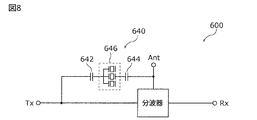
図8は、特許文献1に記載されたデュプレクサの回路構成図である。同図に示されたデュプレクサ600は、分波器と、キャンセル回路640とを備える。分波器は、送信側フィルタ回路と受信側フィルタ回路とを有している。キャンセル回路640は、縦結合型弾性波共振器646と、静電容量642および644とで構成され、送信側フィルタ回路を流れる所定の周波数帯域の成分に対して、逆位相かつ同振幅の相殺成分を生成する。上記構成により、挿入損失を増大させることなく、分波器のアイソレーション特性またはフィルタの減衰特性を向上させることができるとしている。
FIG. 8 is a circuit configuration diagram of the duplexer described in
しかしながら、特許文献1に記載されたデュプレクサ600では、縦結合型弾性波共振器646のアンテナ端子側および送信端子側の両方に静電容量642および644が配置されているので、キャンセル回路640を含むデュプレクサ600が大型化してしまう。さらに、キャンセル回路640に必要な静電容量を確保しつつ、キャンセル回路640の容量素子を縦結合型弾性波共振器646の両側に直列分配すると、容量素子1つあたりの静電容量が大きくなり、インピーダンスが下がってしまう。このため、受信側フィルタの通過帯域と縦結合型弾性波共振器646の共振レスポンス帯域とが重なってしまう場合に、受信側フィルタにおいて通過帯域内リップルを発生させ、帯域幅を減少させてしまう。
However, in the
そこで、本発明は、上記課題を解決するためになされたものであって、キャンセル回路が並列接続された第1フィルタ回路の減衰特性を改善するとともに、第1フィルタ回路と共通端子で接続された第2フィルタ回路の通過特性を改善する小型のマルチプレクサを提供することを目的とする。 Therefore, the present invention has been made to solve the above-described problem, and improves the attenuation characteristics of the first filter circuit in which the cancel circuit is connected in parallel, and is connected to the first filter circuit at a common terminal. An object of the present invention is to provide a small multiplexer that improves the pass characteristic of the second filter circuit.
上記目的を達成するために、本発明の一態様に係るマルチプレクサは、高周波信号が入出力される共通端子、第1端子および第2端子と、第1周波数帯域を通過帯域とし、前記共通端子および前記第1端子に接続された第1フィルタ回路と、前記第1周波数帯域と異なる第2周波数帯域を通過帯域とし、前記共通端子および前記第2端子に接続された第2フィルタ回路と、前記共通端子と前記第1端子とを結ぶ経路上にあって前記共通端子側に位置する第1ノードおよび前記第1端子側に位置する第2ノードに接続され、前記経路上を流れる所定の周波数帯域の成分を相殺するためのキャンセル回路と、を備え、前記キャンセル回路は、一端が前記第1ノードに接続された容量素子と、一端が前記容量素子の他端に接続され、他端が容量素子を介さずに前記第2ノードに接続された縦結合型共振器と、を有し、前記第1ノード側から前記キャンセル回路を見た場合の前記第2周波数帯域におけるインピーダンスは、前記第2ノード側から前記キャンセル回路を見た場合の前記第2周波数帯域におけるインピーダンスよりも高い。 In order to achieve the above object, a multiplexer according to one aspect of the present invention includes a common terminal for inputting and outputting a high-frequency signal, a first terminal and a second terminal, a first frequency band as a pass band, and the common terminal and A first filter circuit connected to the first terminal, a second frequency band different from the first frequency band as a pass band, a second filter circuit connected to the common terminal and the second terminal, and the common A predetermined frequency band flowing on the path connected to the first node located on the common terminal side and the second node located on the first terminal side on a path connecting the terminal and the first terminal. A cancel circuit for canceling a component, wherein the cancel circuit has one end connected to the first node, one end connected to the other end of the capacitative element, and the other end connected to the capacitative element A longitudinally coupled resonator connected to the second node without intervening, and the impedance in the second frequency band when the cancel circuit is viewed from the first node side is the second node side Higher than the impedance in the second frequency band when the cancel circuit is viewed.
第1フィルタ回路の所定の周波数帯域における減衰特性を改善すべく、上記経路上を流れる所定の周波数帯域の成分に対する相殺成分を生成するキャンセル回路が、第1フィルタ回路に並列接続される。このキャンセル回路としては、上記所定の周波数帯域のみを低損失とすることに有利な縦結合型共振器が用いられる。ここで、上記相殺成分を、上記経路上の上記成分と同振幅かつ逆位相に調整するため、キャンセル回路には、振幅および位相調整用の容量素子が直列付加される。キャンセル回路に直列付加される容量素子としては、第1フィルタ回路とキャンセル回路とのインピーダンス整合を考慮して、縦結合型共振器の両端に分配配置されることが考えられる。 In order to improve the attenuation characteristic of the first filter circuit in a predetermined frequency band, a cancel circuit that generates a canceling component for the component of the predetermined frequency band flowing on the path is connected in parallel to the first filter circuit. As the cancel circuit, a longitudinally coupled resonator that is advantageous for reducing the loss only in the predetermined frequency band is used. Here, in order to adjust the cancellation component to the same amplitude and opposite phase as the component on the path, a capacitance element for amplitude and phase adjustment is added in series to the cancel circuit. It is conceivable that the capacitive element added in series with the cancel circuit is distributed at both ends of the longitudinally coupled resonator in consideration of impedance matching between the first filter circuit and the cancel circuit.
これに対して、本構成によれば、キャンセル回路の容量素子は、縦結合型共振器の第2ノード側には配置されず、第1ノード側のみに配置される。これにより、容量素子が縦結合型共振器の両端に分配配置された場合(容量素子が2つ直列配置された場合)と同じ静電容量を確保するには、直列配置された2つの容量素子の1つよりも小さな静電容量を有する容量素子を、縦結合共振器の共通端子側のみに配置すればよい。これにより、2つの容量素子が配置されたキャンセル回路と比較して、キャンセル回路を小型化できる。 On the other hand, according to this configuration, the capacitive element of the cancel circuit is not disposed on the second node side of the longitudinally coupled resonator, but is disposed only on the first node side. Thus, in order to secure the same capacitance as when the capacitive elements are distributed and arranged at both ends of the longitudinally coupled resonator (when two capacitive elements are arranged in series), two capacitive elements arranged in series A capacitive element having an electrostatic capacity smaller than one of these may be disposed only on the common terminal side of the longitudinally coupled resonator. Accordingly, the cancel circuit can be reduced in size as compared with the cancel circuit in which the two capacitive elements are arranged.
また、所定の静電容量が必要なキャンセル回路において、容量素子を縦結合共振器の共通端子側の第1ノード側のみに配置することにより、第1ノード側からキャンセル回路を見た場合のインピーダンスを、第2ノード側からキャンセル回路を見た場合のインピーダンスよりも大きくできる。ここで、本構成では、キャンセル回路の上記インピーダンスを、第2フィルタ回路の通過帯域(第2周波数帯域)におけるインピーダンスとしている。このため、共通端子から入力された第2周波数帯域の信号が第1フィルタ側に漏洩することを抑制できる。 Further, in a cancel circuit that requires a predetermined capacitance, an impedance when the cancel circuit is viewed from the first node side by disposing the capacitive element only on the first node side on the common terminal side of the longitudinally coupled resonator. Can be made larger than the impedance when the cancel circuit is viewed from the second node side. Here, in this configuration, the impedance of the cancel circuit is the impedance in the pass band (second frequency band) of the second filter circuit. For this reason, it can suppress that the signal of the 2nd frequency band input from the common terminal leaks to the 1st filter side.
以上より、マルチプレクサ回路を小型化しつつ、第1フィルタ回路の減衰特性を改善するとともに第2フィルタ回路の通過特性を改善できる。 As described above, it is possible to improve the attenuation characteristic of the first filter circuit and the pass characteristic of the second filter circuit while reducing the size of the multiplexer circuit.
また、前記第1ノードは、前記共通端子であってもよい。 The first node may be the common terminal.
これにより、所定の静電容量が必要なキャンセル回路において、容量素子を縦結合共振器の共通端子側のみに配置することにより、共通端子側からキャンセル回路を見た場合のインピーダンスを、第2ノード側からキャンセル回路を見た場合のインピーダンスよりも大きくできる。よって、共通端子から入力された第2周波数帯域の信号が第1フィルタ側に漏洩することを、より効果的に抑制できる。 As a result, in the cancel circuit that requires a predetermined capacitance, the impedance when the cancel circuit is viewed from the common terminal side is obtained by arranging the capacitive element only on the common terminal side of the longitudinally coupled resonator. It can be larger than the impedance when the cancel circuit is viewed from the side. Therefore, it can suppress more effectively that the signal of the 2nd frequency band input from the common terminal leaks to the 1st filter side.
また、前記第1周波数帯域は、前記第2周波数帯域よりも低周波数側に位置し、前記所定の周波数帯域は、前記第2周波数帯域に含まれ、前記縦結合型共振器の挿入損失が極小となる周波数は、前記第2周波数帯域近傍に位置してもよい。 The first frequency band is located on a lower frequency side than the second frequency band, the predetermined frequency band is included in the second frequency band, and the insertion loss of the longitudinally coupled resonator is minimal. May be located in the vicinity of the second frequency band.
第1フィルタ回路の通過帯域(第1周波数帯域)よりも高周波側の減衰特性を改善するために、縦結合型共振器の挿入損失が極小となる周波数を含む上記所定の周波数帯域を、第2周波数帯域に設定した場合、第2フィルタ回路の通過特性が劣化することが懸念される。これに対して、共通端子側(第1ノード)からキャンセル回路を見た場合の第2周波数帯域におけるインピーダンスは、第2ノード側からキャンセル回路を見た場合の第2周波数帯域におけるインピーダンスよりも高いので、第2フィルタ回路の通過特性を改善できる。さらに、第1フィルタ回路の第2周波数帯域における減衰特性が改善されるので、第1フィルタ回路と第2フィルタ回路とのアイソレーション特性が改善される。また、第1周波数帯域に、上記所定の周波数帯域が設定されないので、第1フィルタ回路の通過特性の劣化が回避される。 In order to improve the attenuation characteristic on the higher frequency side than the pass band (first frequency band) of the first filter circuit, the predetermined frequency band including the frequency at which the insertion loss of the longitudinally coupled resonator is minimized is set to the second frequency band. When the frequency band is set, there is a concern that the pass characteristic of the second filter circuit deteriorates. On the other hand, the impedance in the second frequency band when the cancel circuit is viewed from the common terminal side (first node) is higher than the impedance in the second frequency band when the cancel circuit is viewed from the second node side. Therefore, the pass characteristic of the second filter circuit can be improved. Furthermore, since the attenuation characteristic in the second frequency band of the first filter circuit is improved, the isolation characteristic between the first filter circuit and the second filter circuit is improved. In addition, since the predetermined frequency band is not set in the first frequency band, deterioration of the pass characteristic of the first filter circuit is avoided.
また、前記第1フィルタ回路は、複数の弾性波共振子で構成されたラダー型の弾性波フィルタ回路であってもよい。 The first filter circuit may be a ladder-type elastic wave filter circuit including a plurality of elastic wave resonators.
第1フィルタ回路が、ラダー型の弾性波フィルタ回路である場合、第1フィルタ回路の減衰帯域では位相が複雑に変化しないので、第1フィルタ回路の上記経路上を流れる成分と逆位相の成分を、縦結合型共振器で形成しやすい。よって、第1フィルタ回路の減衰特性の改善効果、および、第1フィルタ回路と第2フィルタ回路とのアイソレーション特性の改善効果が、より発揮される。 When the first filter circuit is a ladder-type elastic wave filter circuit, the phase does not change in a complicated manner in the attenuation band of the first filter circuit. Therefore, the component having the opposite phase to the component flowing on the path of the first filter circuit is obtained. It is easy to form with a longitudinally coupled resonator. Therefore, the improvement effect of the attenuation characteristic of the first filter circuit and the improvement effect of the isolation characteristic between the first filter circuit and the second filter circuit are more exhibited.
また、前記第1フィルタ回路は、前記第1端子から前記共通端子へ高周波信号を伝搬する送信側フィルタであり、前記第2フィルタ回路は、前記共通端子から前記第2端子へ高周波信号を伝搬する受信側フィルタであり、前記経路上であって、前記第1端子と前記第2ノードとの間には、直列腕共振子が接続されていてもよい。 The first filter circuit is a transmission-side filter that propagates a high-frequency signal from the first terminal to the common terminal, and the second filter circuit propagates a high-frequency signal from the common terminal to the second terminal. A series arm resonator may be connected between the first terminal and the second node on the path.
これにより、送信側フィルタおよび受信側フィルタが共通端子で接続されたデュプレクサが構成される。ここで、送信側端子(第1端子)から印加された電力およびサージは、直列腕共振子を最初に通過することとなるため、キャンセル回路の縦結合型共振器に印加される信号強度が小さくなる。つまり、デュプレクサの耐電力性および耐サージ性を高めることが可能となる。 As a result, a duplexer in which the transmission side filter and the reception side filter are connected by the common terminal is configured. Here, since the power and surge applied from the transmission side terminal (first terminal) first pass through the series arm resonator, the signal strength applied to the longitudinally coupled resonator of the cancel circuit is small. Become. That is, it becomes possible to improve the power resistance and surge resistance of the duplexer.
また、前記第1フィルタ回路は、圧電性を有する基板上に形成された複数の第1IDT電極で構成された弾性表面波フィルタであり、前記縦結合型共振器は、前記基板上に形成された複数の第2IDT電極で構成された弾性表面波共振器であってもよい。 The first filter circuit is a surface acoustic wave filter including a plurality of first IDT electrodes formed on a piezoelectric substrate, and the longitudinally coupled resonator is formed on the substrate. A surface acoustic wave resonator including a plurality of second IDT electrodes may be used.
これにより、第1フィルタ回路と縦結合型共振器とが、同じ圧電基板上に形成された弾性表面波共振子で構成されるので、マルチプレクサを小型化できる。 As a result, the first filter circuit and the longitudinally coupled resonator are composed of surface acoustic wave resonators formed on the same piezoelectric substrate, so that the multiplexer can be miniaturized.
また、前記容量素子は、前記基板上に形成された櫛歯状電極で構成されていてもよい。 The capacitive element may be composed of comb-like electrodes formed on the substrate.
これにより、第1フィルタ回路とキャンセル回路とが、同じ圧電基板上に形成されるので、マルチプレクサを小型化できる。 Thereby, since the first filter circuit and the cancel circuit are formed on the same piezoelectric substrate, the multiplexer can be miniaturized.
また、前記複数の第1IDT電極は、第1電極膜で形成され、前記複数の第1IDT電極を接続する第1配線は、前記第1電極膜と第2電極膜との積層体で形成され、前記第1ノード、前記容量素子、前記複数の第2IDT電極、および前記第2ノードを接続する第2配線は、前記第1電極膜と同一の膜厚を有してもよい。 The plurality of first IDT electrodes are formed of a first electrode film, and the first wiring connecting the plurality of first IDT electrodes is formed of a stacked body of the first electrode film and the second electrode film, The first node, the capacitor, the plurality of second IDT electrodes, and the second wiring connecting the second node may have the same film thickness as the first electrode film.
第1IDT(InterDigital Transducer)電極間を接続する第1配線は、第1フィルタ回路の通過帯域における低損失性を確保すべく、2層配線で構成されている。これに対して、キャンセル回路の第2配線は、キャンセル回路を流れる相殺成分が小振幅であることから、抵抗分が増えても大きな問題は生じないので単層配線でよい。よって、第2配線を細線化できるので、チップサイズを小型化できる。 The first wiring that connects between the first IDT (InterDigital Transducer) electrodes is composed of a two-layer wiring to ensure low loss in the pass band of the first filter circuit. On the other hand, the second wiring of the cancellation circuit may be a single-layer wiring because the canceling component flowing through the cancellation circuit has a small amplitude, so that a large problem does not occur even if the resistance increases. Therefore, since the second wiring can be thinned, the chip size can be reduced.
また、前記第1フィルタ回路は、直列腕共振子と並列腕共振子とで構成されたラダー型の弾性表面波フィルタであり、前記基板の平面視において、前記縦結合型共振器における弾性表面波の伝搬経路を伝搬方向に延長した領域は、前記並列腕共振子における弾性表面波の伝搬経路および前記直列腕共振子における弾性表面波の伝搬経路と重ならなくてもよい。 The first filter circuit is a ladder-type surface acoustic wave filter including a series arm resonator and a parallel arm resonator, and the surface acoustic wave in the longitudinally coupled resonator in a plan view of the substrate. The region obtained by extending the propagation path in the propagation direction may not overlap the surface acoustic wave propagation path in the parallel arm resonator and the surface acoustic wave propagation path in the series arm resonator.
キャンセル回路で生成される相殺成分は小振幅であるため、縦結合型共振器と、第1フィルタ回路の直列腕共振子および並列腕共振子との伝送路を並べて配置すると、上記相殺成分が上記直列腕共振子および並列腕共振子の弾性表面波に干渉され、上記相殺成分の位相特性が影響されて、第1フィルタ回路の減衰特性が悪化する。これに対して、上記構成によれば、第1フィルタ回路の減衰特性を改善できる。 Since the cancellation component generated by the cancellation circuit has a small amplitude, if the transmission path of the longitudinally coupled resonator and the series arm resonator and the parallel arm resonator of the first filter circuit are arranged side by side, the cancellation component is The attenuation characteristics of the first filter circuit deteriorate due to interference with the surface acoustic waves of the series arm resonator and the parallel arm resonator and the phase characteristics of the canceling component. On the other hand, according to the above configuration, the attenuation characteristic of the first filter circuit can be improved.
また、前記第2フィルタ回路は、前記基板上に形成された複数の第3IDT電極で構成された弾性表面波フィルタであり、前記縦結合型共振器に接続されるグランド配線は、前記第1フィルタ回路に接続されるグランド電極と前記基板上で接続され、前記第2フィルタ回路に接続されるグランド電極と前記基板上で接続されなくてもよい。 The second filter circuit is a surface acoustic wave filter formed of a plurality of third IDT electrodes formed on the substrate, and a ground wiring connected to the longitudinally coupled resonator is the first filter. The ground electrode connected to the circuit may be connected on the substrate, and the ground electrode connected to the second filter circuit may not be connected on the substrate.
これにより、縦結合型共振器に接続されるグランド配線が、第1フィルタ回路に接続さグランド電極に接続されているので、縦結合型共振器と第1フィルタ回路とのグランド電極を圧電基板上で共有でき、チップサイズの小型化が可能となる。一方、縦結合型共振器に接続されるグランド配線が、第2フィルタ回路に接続されるグランド電極に接続されていないので、縦結合型共振器のレスポンスがグランド電極を介して第2フィルタに回り込むことを回避できるので、第2フィルタ回路の通過特性の劣化を回避できる。 Thus, since the ground wiring connected to the longitudinally coupled resonator is connected to the ground electrode connected to the first filter circuit, the ground electrode of the longitudinally coupled resonator and the first filter circuit is placed on the piezoelectric substrate. The chip size can be reduced. On the other hand, since the ground wiring connected to the longitudinally coupled resonator is not connected to the ground electrode connected to the second filter circuit, the response of the longitudinally coupled resonator wraps around the second filter via the ground electrode. Therefore, it is possible to avoid the deterioration of the pass characteristic of the second filter circuit.
本発明によれば、キャンセル回路が並列接続された第1フィルタ回路の減衰特性が改善されるとともに、第1フィルタ回路と共通端子で接続された第2フィルタ回路の通過特性が改善された小型のマルチプレクサを提供することが可能となる。 According to the present invention, the attenuation characteristic of the first filter circuit connected in parallel with the cancel circuit is improved, and the pass characteristic of the second filter circuit connected to the first filter circuit at the common terminal is improved. A multiplexer can be provided.
以下、本発明の実施の形態について、実施例および図面を用いて詳細に説明する。なお、以下で説明する実施例は、いずれも包括的または具体的な例を示すものである。以下の実施例で示される数値、形状、材料、構成要素、構成要素の配置および接続形態などは、一例であり、本発明を限定する主旨ではない。以下の実施例における構成要素のうち、独立請求項に記載されていない構成要素については、任意の構成要素として説明される。また、図面に示される構成要素の大きさまたは大きさの比は、必ずしも厳密ではない。 Hereinafter, embodiments of the present invention will be described in detail with reference to examples and drawings. It should be noted that any of the embodiments described below is a comprehensive or specific example. Numerical values, shapes, materials, constituent elements, arrangement of constituent elements, connection forms, and the like shown in the following examples are merely examples, and are not intended to limit the present invention. Among the constituent elements in the following embodiments, constituent elements not described in the independent claims are described as arbitrary constituent elements. In addition, the size or size ratio of the components shown in the drawings is not necessarily strict.
(実施の形態)
[1.マルチプレクサの基本回路構成]
図1は、実施の形態に係るマルチプレクサ1およびその周辺回路の回路構成図である。同図には、本実施の形態に係るマルチプレクサ1と、アンテナ素子2と、整合用インダクタ3とが示されている。
(Embodiment)
[1. Basic circuit configuration of multiplexer]
FIG. 1 is a circuit configuration diagram of a
マルチプレクサ1は、送信側フィルタ10と、受信側フィルタ20と、キャンセル回路30と、共通端子100と、送信側端子(第1端子)110と、受信側端子(第2端子)120とを備える。送信側フィルタ10と受信側フィルタ20とは、共通端子100で共通接続されている。この構成により、マルチプレクサ1は、アンテナ素子2にて受信した高周波信号を、共通端子100および受信側フィルタ20を経由して受信側端子120から出力し、送信側端子110から入力された高周波信号を送信側フィルタ10および共通端子100を経由してアンテナ素子2へ出力するデュプレクサとして機能する。
The
なお、送信側端子110および受信側端子120には、高周波信号を増幅する増幅回路または高周波信号処理回路(RFIC)などが接続される。また、共通端子100は、アンテナ素子2に接続されている必要はなく、スイッチ回路を介してアンテナ素子2に接続されていてもよい。また、共通端子100と、送信側フィルタ10および受信側フィルタ20との間に、インピーダンス整合用のインダクタまたはキャパシタなどが挿入されていてもよい。
Note that an amplifier circuit or a high frequency signal processing circuit (RFIC) that amplifies a high frequency signal is connected to the
送信側フィルタ10は、第1周波数帯域を通過帯域とし、共通端子100および送信側端子110に接続された第1フィルタ回路である。
The transmission-
受信側フィルタ20は、第1周波数帯域と異なる第2周波数帯域を通過帯域とし、共通端子100および受信側端子120に接続された第2フィルタ回路である。
The reception-
なお、第1周波数帯域と第2周波数帯域との周波数の高低関係はいずれであってもよいが、本実施の形態では、第2周波数帯域が第1周波数帯域よりも高い、つまり、受信側フィルタ20の通過帯域が、送信側フィルタ10の通過帯域よりも高い回路構成を例示する。
The frequency relationship between the first frequency band and the second frequency band may be any, but in the present embodiment, the second frequency band is higher than the first frequency band, that is, the reception side filter. A circuit configuration in which 20 passbands are higher than the passband of the
キャンセル回路30は、共通端子100(第1ノード)、および、共通端子100と送信側端子110とを結ぶ経路上のノードN(第2ノード)に接続され、当該経路上を流れる所定の周波数帯域の成分を相殺するための回路である。
The cancel
より具体的には、キャンセル回路30は、縦結合型共振器31と、容量素子32とを備える。縦結合型共振器31は、弾性波共振子31aおよび31bで構成され、一端(弾性波共振子31a)が容量素子32の他端に接続され、他端(弾性波共振子31b)が容量素子を介さずにノードNに接続されている。容量素子32は、一端が共通端子100に接続されている。
More specifically, the cancel
ここで、共通端子100側からキャンセル回路30を見た場合の第2周波数帯域におけるインピーダンスは、ノードN側からキャンセル回路30を見た場合の第2周波数帯域におけるインピーダンスよりも高い。
Here, the impedance in the second frequency band when the cancel
上記構成によれば、送信側フィルタ10の第1周波数帯域よりも高周波側における所定の周波数帯域の減衰特性を改善すべく、上記経路上を流れる所定の周波数帯域の成分の相殺成分を生成するキャンセル回路30が、送信側フィルタ10に並列接続されている。キャンセル回路30としては、広帯域にわたる他の周波数帯域と比して上記所定の周波数帯域のみを低損失とすることに有利な縦結合型共振器31が用いられる。ここで、上記相殺成分を、上記経路上を流れる所定の周波数帯域の上記成分と同振幅かつ逆位相に調整するため、キャンセル回路30には、振幅および位相調整用の容量素子32が直列付加されている。
According to the above configuration, in order to improve the attenuation characteristic of the predetermined frequency band on the higher frequency side than the first frequency band of the
キャンセル回路に直列付加される容量素子としては、一般に、キャンセル回路が並列接続されるフィルタ回路とキャンセル回路とのインピーダンス整合を考慮して、縦結合型共振器の両端に分配配置されることが考えられる。 In general, the capacitive element added in series to the cancel circuit is distributed at both ends of the longitudinally coupled resonator in consideration of impedance matching between the cancel circuit and the filter circuit connected in parallel. It is done.
これに対して、本実施の形態に係るマルチプレクサ1の構成によれば、キャンセル回路30の容量素子は、縦結合型共振器31のノードN側には配置されず、共通端子100側のみに配置される。これにより、容量素子が縦結合型共振器の両端に分配配置された従来構成(容量素子が2つ直列配置された場合)と同じ静電容量を確保するには、直列配置された2つの容量素子の1つよりも小さな静電容量を有する容量素子32を、縦結合型共振器31の共通端子100側のみに配置すればよい。これにより、2つの容量素子が配置された従来のキャンセル回路と比較して、キャンセル回路30を小型化できる。
On the other hand, according to the configuration of the
また、所定の静電容量が必要なキャンセル回路において、容量素子32を縦結合型共振器31の共通端子100側のみに配置することにより、共通端子100側からキャンセル回路30を見た場合のインピーダンスを、ノードN側からキャンセル回路30を見た場合のインピーダンスよりも大きくできる。ここで、本実施の形態に係るマルチプレクサ1では、キャンセル回路30の上記インピーダンスを、受信側フィルタ20の通過帯域(第2周波数帯域)におけるインピーダンスとしている。つまり、共通端子100側からキャンセル回路30を見た場合の第2周波数帯域におけるインピーダンスは、ノードN側からキャンセル回路30を見た場合の第2周波数帯域におけるインピーダンスよりも大きい。このため、共通端子100から入力された第2周波数帯域の信号が送信側フィルタ10の方へ漏洩することを抑制できる。
Further, in a cancel circuit that requires a predetermined capacitance, the
以上より、マルチプレクサ1を小型化しつつ、送信側フィルタ10の上記所定の周波数帯域の減衰特性を改善するとともに、受信側フィルタ20の通過特性を改善することが可能となる。
As described above, it is possible to improve the attenuation characteristic of the
なお、本実施の形態では、キャンセル回路30は、共通端子100、および、ノードNに接続された構成を例示したが、本発明に係るキャンセル回路は、共通端子100に直接接続されず、送信側フィルタ10を構成する直列腕共振子12s1〜14s2を結ぶ各直列腕上のノード(第1ノード)と、ノードN(第2ノード)とに接続されていてもよい。つまり、キャンセル回路は、共通端子100と送信側端子110とを結ぶ経路上にあって共通端子100側に位置する第1ノードおよび送信側端子110側に位置する第2ノードに接続されていればよい。この構成においても、本実施の形態に係るキャンセル回路30およびマルチプレクサ1が有する効果と同様の効果が奏され、送信側フィルタ10の上記所定の周波数帯域の減衰特性を改善するとともに、受信側フィルタ20の通過特性を改善することが可能となる。
In the present embodiment, the cancel
以下、本実施の形態に係るマルチプレクサ1の具体的回路構成例を示し、マルチプレクサ1について詳細に説明する。
Hereinafter, a specific circuit configuration example of the
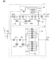
[2.マルチプレクサの回路構成例]
図2は、実施例に係るマルチプレクサ1の具体的回路構成の一例を示す図である。同図に示されたマルチプレクサ1は、図1と同様に、送信側フィルタ10と、受信側フィルタ20と、キャンセル回路30と、共通端子100と、送信側端子110と、受信側端子120とを備える。
[2. Example of multiplexer circuit configuration]
FIG. 2 is a diagram illustrating an example of a specific circuit configuration of the
送信側フィルタ10は、複数の弾性波共振子で構成されたラダー型の弾性波フィルタ回路であり、直列腕共振子11s、12s1、12s2、13s1、13s2、14s1および14s2と、並列腕共振子11p、12p1、12p2および13pと、を備える。本構成により、送信側フィルタ10は、例えば、LTE(Long Term Evolution)規格のBand8の送信フィルタ(送信(第1周波数)帯域:880−915MHz)に適用される。
The transmission-
送信側フィルタ10がラダー型の弾性波フィルタ回路であることにより、送信側フィルタ10の減衰帯域では位相が複雑に変化しないので、送信側フィルタ10の上記経路上を流れる成分に対して逆位相の成分を、縦結合型共振器31で形成しやすい。よって、送信側フィルタ10の減衰特性の改善効果、および、送信側フィルタ10と受信側フィルタ20とのアイソレーション特性の改善効果が、より発揮される。
Since the transmission-
さらに、直列腕共振子11s〜14s2および並列腕共振子11p〜13pのそれぞれは、圧電基板上に形成されたIDT電極で構成されている。つまり、送信側フィルタ10は、上記圧電基板上に形成された複数の第1IDT電極で構成された弾性表面波フィルタである。
Further, each of the
受信側フィルタ20は、複数の弾性波共振子で構成された弾性波フィルタ回路であり、直列腕共振子21sおよび22sと、並列腕共振子21pおよび22pと、縦結合型共振器23Lとを備える。縦結合型共振器23Lは、並列接続された縦結合型共振器23L1および23L2で構成され、縦結合型共振器23L1および23L2のそれぞれは、弾性波伝搬方向に沿って並べられた5つの弾性波共振子で構成されている。本構成により、受信側フィルタ20は、例えば、LTE規格のBand8の受信フィルタ(受信(第2周波数)帯域:925−960MHz)に適用される。なお、直列腕共振子21sおよび22s、並列腕共振子21pおよび22p、ならびに縦結合型共振器23Lを構成する弾性波共振子のそれぞれは、圧電基板上に形成されたIDT電極で構成されている。つまり、受信側フィルタ20は、圧電基板上に形成された複数のIDT電極で構成された弾性表面波フィルタである。
The reception-
キャンセル回路30は、縦結合型共振器31と、容量素子32とを備える。なお、図2では、容量素子32を弾性波共振子で表しているが、これは、容量素子32は、弾性表面波共振子(例えば、1ポート共振器)のような容量性を有する弾性波共振子で実現してもよいという意味である。
The cancel
縦結合型共振器31は、弾性波伝搬方向に沿って並べられた2つの弾性波共振子31aおよび31bで構成されている。縦結合型共振器31の一端(弾性波共振子31a)が容量素子32の他端に接続され、縦結合型共振器31の他端(弾性波共振子31b)が容量素子を介さずにノードNに接続されている。さらに、弾性波共振子31aおよび31bのそれぞれは、送信側フィルタ10が形成された圧電基板上に形成されたIDT電極で構成されている。つまり、キャンセル回路30は、上記圧電基板上に形成された複数の第2IDT電極で構成された弾性表面波共振器である。弾性波共振子31aを構成するIDT電極は、互いに対向する2つの櫛形電極で構成されており、一方の櫛形電極は容量素子32の他端に接続され、他方の櫛形電極はグランド電極に接続されている。また、弾性波共振子31bを構成するIDT電極は、互いに対向する2つの櫛形電極で構成されており、一方の櫛形電極はノードNに接続され、他方の櫛形電極はグランド電極に接続されている。
The longitudinally coupled
送信側フィルタ10と縦結合型共振器31とが、同一の圧電基板上に形成されていることにより、マルチプレクサ1を小型化できる。
Since the
なお、本実施例では、ノードNと送信側端子110との間に、送信側フィルタ10を構成する直列腕共振子11sが配置されている。これにより、送信側端子110から印加された電力およびサージは、直列腕共振子11sを最初に通過することとなるため、キャンセル回路30の縦結合型共振器31に印加される信号強度が小さくなる。つまり、マルチプレクサ1の、耐電力性および耐サージ性を高めることが可能となる。
In the present embodiment, a
なお、縦結合型共振器31を構成する弾性波共振子(IDT電極)の個数は、2個に限定されず、キャンセル回路30として必要な通過特性に応じて適宜決定されればよい。
Note that the number of acoustic wave resonators (IDT electrodes) constituting the longitudinally coupled
容量素子32は、一端が共通端子100に接続され、他端が縦結合型共振器31の一端(弾性波共振子31a)に接続されている。なお、容量素子32は、送信側フィルタ10および縦結合型共振器31が形成された圧電基板上に形成された櫛歯状電極で構成されている。
One end of the
送信側フィルタ10、縦結合型共振器31および容量素子32が、同一の圧電基板上に形成されていることにより、マルチプレクサ1を小型化できる。
Since the transmission-
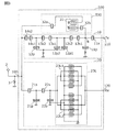
図3は、比較例に係るマルチプレクサ500の具体的回路構成図である。同図に示されたマルチプレクサ500は、送信側フィルタ10と、受信側フィルタ20と、キャンセル回路530と、共通端子100と、送信側端子110と、受信側端子120とを備える。同図に示されたマルチプレクサ500は、実施例に係るマルチプレクサ1と比較して、キャンセル回路の構成のみが異なる。以下、比較例に係るマルチプレクサ500について、実施例に係るマルチプレクサ1と同じ点は説明を省略し、異なる点を中心に説明する。
FIG. 3 is a specific circuit configuration diagram of the
キャンセル回路530は、縦結合型共振器31と、容量素子32aおよび32bとを備える。
Cancel
キャンセル回路530の縦結合型共振器31は、弾性波伝搬方向に沿って並べられた2つの弾性波共振子31aおよび31bで構成されている。縦結合型共振器31の一端(弾性波共振子31a)が容量素子32aの他端に接続され、縦結合型共振器31の他端(弾性波共振子31b)が容量素子32bの他端に接続されている。さらに、弾性波共振子31aおよび31bのそれぞれは、送信側フィルタ10が形成された圧電基板上に形成されたIDT電極で構成されている。弾性波共振子31aを構成するIDT電極は、互いに対向する2つの櫛形電極で構成されており、一方の櫛形電極は容量素子32aの他端に接続され、他方の櫛形電極はグランド電極に接続されている。また、弾性波共振子31bを構成するIDT電極は、互いに対向する2つの櫛形電極で構成されており、一方の櫛形電極は容量素子32bの他端に接続され、他方の櫛形電極はグランド電極に接続されている。
The longitudinally coupled
容量素子32aは、一端が共通端子100に接続され、他端が縦結合型共振器31の一端(弾性波共振子31a)に接続されている。また、容量素子32bは、一端がノードNに接続され、他端が縦結合型共振器31の他端(弾性波共振子31b)に接続されている。
One end of the
一般に、図3に示された比較例に係るマルチプレクサ500の構成のように、キャンセル回路530が並列接続される送信側フィルタ10とキャンセル回路530とのインピーダンス整合を考慮して、縦結合型共振器31の両端に、容量素子32aおよび32bが分配配置される。
In general, as in the configuration of the
これに対して、実施例に係るマルチプレクサ1の構成では、送信側フィルタ10の第1周波数帯域よりも高周波側における所定の周波数帯域の減衰特性を改善すべく、上記経路上を流れる所定の周波数帯域の成分の相殺成分を生成するキャンセル回路30が、送信側フィルタ10に並列接続されている。ここで、上記相殺成分を、上記経路上を流れる第2周波数帯域の上記成分と同振幅かつ逆位相に調整するため、キャンセル回路30には、振幅および位相調整用の容量素子32が直列付加されている。
On the other hand, in the configuration of the
本実施例に係るマルチプレクサ1の構成によれば、キャンセル回路30の容量素子32は、縦結合型共振器31のノードN側には配置されず、共通端子100側のみに配置される。これにより、容量素子32aおよび32bが縦結合型共振器31の両端に分配(直列)配置された比較例と同じ静電容量を確保するには、直列配置された2つの容量素子32aおよび32bのいずれかよりも小さな静電容量を有する容量素子32を、縦結合型共振器31の共通端子100側のみに配置すればよい。
According to the configuration of the
これにより、2つの容量素子32aおよび32bが、縦結合型共振器31の両端に分配(直列)配置された従来のキャンセル回路530と比較して、キャンセル回路30を小型化できる。
As a result, the cancel
また、所定の静電容量が必要なキャンセル回路において、容量素子32を縦結合型共振器31の共通端子100側のみに配置することにより、共通端子100側からキャンセル回路30を見た場合のインピーダンスを、ノードN側からキャンセル回路30を見た場合のインピーダンスよりも大きくできる。ここで、本実施例に係るマルチプレクサ1では、キャンセル回路30の上記インピーダンスを、受信側フィルタ20の通過帯域(第2周波数帯域)におけるインピーダンスとしている。つまり、共通端子100側からキャンセル回路30を見た場合の第2周波数帯域におけるインピーダンスは、ノードN側からキャンセル回路30を見た場合の第2周波数帯域におけるインピーダンスよりも大きい。このため、共通端子100から入力された第2周波数帯域の信号が送信側フィルタ10の方へ漏洩することを抑制できる。
Further, in a cancel circuit that requires a predetermined capacitance, the
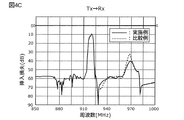
[3.実施例および比較例に係るマルチプレクサの特性比較]
図4Aは、実施例および比較例に係る送信側フィルタ10の通過特性を比較したグラフである。また、図4Bは、実施例および比較例に係る受信側フィルタ20の通過特性を比較したグラフである。また、図4Cは、実施例および比較例に係るマルチプレクサのアイソレーション特性を比較したグラフである。また、図5は、実施例に係るキャンセル回路30の通過特性を表すグラフである。また、表1に、実施例および比較例に係るキャンセル回路の電極パラメータを示す。
[3. Comparison of characteristics of multiplexers according to examples and comparative examples]
FIG. 4A is a graph comparing the pass characteristics of the transmission-

ここで、本実施例では、送信側フィルタ10の通過帯域(第1周波数帯域)は、受信側フィルタ20の通過帯域(第2周波数帯域)よりも低周波数側に位置し、キャンセル回路30の挿入損失極小点を有する共振レスポンス周波数は、第2周波数帯域の高域端に位置する。
Here, in this embodiment, the pass band (first frequency band) of the
まず、図4Aに示すように、実施例および比較例に係る送信側フィルタ10の送信側端子110−共通端子100における通過特性は、送信帯域(880−915MHz)において良好な通過特性を有している。また、受信帯域(925−960MHz)においても、実施例および比較例において良好な減衰特性が確保されている。また、図4Cに示すように、実施例および比較例における送受信フィルタ間のアイソレーション特性は、送信帯域(880−915MHz)および受信帯域(925−960MHz)において良好な特性となっている。これは、実施例および比較例に係るキャンセル回路が、(1)960MHz近傍に挿入損失の極小点を有する共振レスポンスを有する、(2)容量素子により送信側フィルタ10を通過する960MHz近傍の成分と同振幅および逆位相の相殺成分が生成される、ことにより、送信側フィルタ10の減衰特性改善および送受信アイソレーション特性改善に対しては、有効に機能していると判断できる。
First, as shown in FIG. 4A, the transmission characteristics at the transmission-
これに対して、図4Bに示すように、実施例および比較例に係る受信側フィルタ20の受信側端子120−共通端子100における通過特性の比較では、比較例に係る受信側フィルタ20の方が、通過帯域における帯域幅が狭くなっている。具体的には、比較例では、受信帯域の高域チャネル側近傍のロスが劣化している。例えば、挿入損失2.0dBの帯域幅で比較すると、実施例では41.8MHzの帯域幅であるのに対して、比較例では40.9MHzの帯域幅となっている。つまり、実施例のほうが広帯域となっている。特に、弾性表面波フィルタの場合、温度変化による特性変化を考慮して帯域幅を確保する必要があるため、この帯域幅の差異は大きなフィルタ特性の差異となる。
On the other hand, as shown in FIG. 4B, in the comparison of the pass characteristics at the reception-side terminal 120-
比較例に係る容量素子32aの静電容量(交叉幅×対数)は、実施例に係る容量素子32の静電容量(交叉幅×対数)より大きく、インピーダンスが低くなっている。このため、受信側フィルタ20が、キャンセル回路530の縦結合型共振器31で発生させた高域チャネル側近傍(960MHz近傍)の共振レスポンスの影響を受けやすくなる。つまり、キャンセル回路530の共通端子側から見たインピーダンスが、キャンセル回路530のノードN側から見たインピーダンスよりも高く設定されていない。このため、高域チャネル側近傍の高周波成分がキャンセル回路530へ漏洩してしまい、受信側フィルタ20への当該高周波成分の伝搬ロスを大きくしてしまう。これにより、共通端子100を通して受信側フィルタ20の通過帯域の高域側に上記共振レスポンスに起因したリップルが発生し、帯域幅が狭くなる。
The capacitance (crossover width × logarithm) of the
これに対して、実施例では、縦結合型共振器31のノードN側には容量素子がなく、その代わりに、縦結合型共振器31の共通端子100側に、比較例に係る容量素子32aよりも静電容量(交叉幅×対数)の小さい容量素子32が付加されている。つまり、キャンセル回路30の共通端子100側から見たインピーダンスが、キャンセル回路30のノードN側から見たインピーダンスよりも高く設定されている。このため、高域チャネル側近傍の高周波成分がキャンセル回路30へ漏洩せず、受信側フィルタ20への当該高周波成分の伝搬ロスを小さくできる。これにより、共通端子100を通して受信側フィルタ20の通過帯域の高域側に上記共振レスポンスに起因したリップルの発生を抑制できるので、帯域幅を広く確保できる。
In contrast, in the embodiment, there is no capacitive element on the node N side of the longitudinally coupled
一方、実施例では、ノードNと縦結合型共振器31との間には容量素子が接続されていないが、図5に示すように、縦結合型共振器31の共振レスポンス(960MHz近傍)は、送信通過帯域から高周波側に大きく離れているため、送信側フィルタ10の帯域幅を劣化させることはない。
On the other hand, in the embodiment, no capacitive element is connected between the node N and the longitudinally coupled
また、実施例では、キャンセル回路30には、容量素子が1つしか配置されておらず、送信側フィルタ10の主信号の振幅と合うように、容量素子32だけで振幅を合わせることとなる。このため、比較例と比べて、容量素子32のインピーダンスを高くできる。よって、実施例に係るマルチプレクサ1では、共通端子100と縦結合型共振器31との間にのみ、容量素子32を直列接続する構成により、受信側フィルタ20の帯域幅を劣化させず、かつ、チップサイズの小型化を実現できる。
In the embodiment, only one capacitive element is arranged in the cancel
[4.マルチプレクサの電極レイアウト構成]
図6は、実施の形態に係るマルチプレクサ1の電極レイアウトを表すチップ平面図である。同図に示すように、圧電基板40上に、送信側フィルタ10、受信側フィルタ20、およびキャンセル回路30のIDT電極および櫛歯状電極、ならびにそれらを接続する配線および外部接続電極が配置されている。なお、マルチプレクサ1の各構成要素が1枚の圧電基板40上に形成されていることから、マルチプレクサ1を、WLP(Wafer Level Package)構造で実現することが可能となる。
[4. Multiplexer electrode layout configuration]
FIG. 6 is a chip plan view showing an electrode layout of the
図6に示すように、圧電基板40の表面下方(Y軸負方向)領域に、送信側フィルタ10を構成する直列腕共振子11s〜14s2のIDT電極、並列腕共振子11p〜13pのIDT電極、それらを接続する第1配線、送信側フィルタ10の送信側電極Tx(送信側端子110)、およびグランド電極GNDが形成されている。さらに、圧電基板40の表面下方(Y軸負方向)領域には、キャンセル回路30を構成する縦結合型共振器31のIDT電極、容量素子32の櫛歯状電極、それらを接続する配線、およびグランド電極51(GND)が形成されている。
As shown in FIG. 6, the IDT electrodes of the
また、圧電基板40の表面上方(Y軸正方向)領域に、受信側フィルタ20を構成する直列腕共振子21sおよび22sのIDT電極、並列腕共振子21pおよび22pのIDT電極、縦結合型共振器23LのIDT電極、それらを接続する配線、受信側フィルタ20の受信側電極Rx(受信側端子120)、およびグランド電極GNDが形成されている。
Also, in the region above the surface of the piezoelectric substrate 40 (Y-axis positive direction), the IDT electrodes of the
また、圧電基板40の表面上であって、送信側フィルタ10およびキャンセル回路30が形成された領域と、受信側フィルタ20が形成された領域との間に、アンテナ接続電極(Ant)が配置されている。
An antenna connection electrode (Ant) is disposed on the surface of the
ここで、本実施の形態に係るマルチプレクサ1では、図6に示すように、圧電基板40の平面視において、縦結合型共振器31における弾性表面波の伝搬経路を伝搬方向(X軸方向)に延長した領域Dは、送信側フィルタ10および受信側フィルタ20を構成する並列腕共振子における弾性表面波の伝搬経路および直列腕共振子における弾性表面波の伝搬経路と重ならない。キャンセル回路30で生成される相殺成分は小振幅であるため、縦結合型共振器31と、送信側フィルタ10の直列腕共振子および並列腕共振子との伝送路を並べて配置すると、上記相殺成分が上記直列腕共振子および並列腕共振子の弾性表面波に干渉され、上記相殺成分の位相特性が影響されて、送信側フィルタ10の減衰特性が悪化する。これに対して、上記構成によれば、送信側フィルタ10の減衰特性を改善できる。
Here, in the
また、図6では、容量素子32を構成する櫛歯電極の各電極指は、他のIDT電極の電極指と同じ方向に形成されているが、容量素子32を構成する櫛歯電極の各電極指を、他のIDT電極の電極指の形成方向と交差する方向に形成してもよい。これにより、容量素子32が、他のIDT電極で励振された高周波信号に干渉されることを抑制できる。
Further, in FIG. 6, each electrode finger of the comb electrode constituting the
また、送信側フィルタ10を構成する複数のIDT電極は、第1電極膜で形成されている。一方、送信側フィルタ10を構成する複数のIDT電極を接続する第1配線は、上記第1電極膜と第2電極膜との積層体で形成されている。さらに、キャンセル回路30内において、共通端子100、容量素子32、弾性波共振子31aおよび31bを構成するIDT電極、およびノードNを接続する第2配線は、上記第1電極膜と同一の膜厚を有している。
Further, the plurality of IDT electrodes constituting the
上記第1配線は、送信側フィルタ10の通過帯域における低損失性を確保すべく、2層配線(積層体)で構成されている。これに対して、キャンセル回路30の第2配線は、キャンセル回路30を流れる相殺成分が小振幅であることから、抵抗分が増えても大きな問題は生じないので、単層配線でよい。よって、上記第2配線を細線化できるので、チップサイズを小型化できる。
The first wiring is composed of a two-layer wiring (laminate) in order to ensure low loss in the pass band of the
図7は、実施の形態の変形例に係るマルチプレクサの電極レイアウトを表すチップ平面図である。同図に示された電極レイアウトは、図6に示された電極レイアウトと比較して、キャンセル回路30を構成する縦結合型共振器31および容量素子32の配置レイアウトが異なる。以下、本変形例に係る電極レイアウトについて、図6に示された実施の形態に係る電極レイアウトと同じ点は説明を省略し、異なる点を中心に説明する。
FIG. 7 is a chip plan view showing an electrode layout of a multiplexer according to a modification of the embodiment. The electrode layout shown in the figure is different from the electrode layout shown in FIG. 6 in the arrangement layout of the longitudinally coupled
ここで、本変形例に係るマルチプレクサでは、図7に示すように、圧電基板40の平面視において、縦結合型共振器31における弾性表面波の伝搬経路を伝搬方向に延長した領域は、送信側フィルタ10を構成する並列腕共振子11pにおける弾性表面波の伝搬経路と重なり、送信側フィルタ10を構成する直列腕共振子における弾性表面波の伝搬経路と重ならない。
Here, in the multiplexer according to this modification, as shown in FIG. 7, in the plan view of the
送信側フィルタ10は、直列腕共振子および並列腕共振子からなるラダー型フィルタであるため、並列腕共振子の共振点は通過帯域(第1周波数帯域)の低域側の減衰極を形成し、並列腕共振子の反共振点および直列腕共振子の共振点は通過帯域(第1周波数帯域)を形成し、直列腕共振子の反共振点は通過帯域(第1周波数帯域)の高域側の減衰極を形成する。また、縦結合型共振器31の共振レスポンスは、受信側フィルタ20の通過帯域(第2周波数帯域)の高域端に設定されている。上記のような共振点および反共振点の周波数関係から、縦結合型共振器31の共振レスポンスの周波数は、送信側フィルタ10の直列腕共振子の共振周波数(反共振周波数)と近い関係にあり、送信側フィルタ10の並列腕共振子の共振周波数(反共振周波数)とは遠い関係にある。
Since the transmission-
このため、キャンセル回路30で生成される相殺成分は小振幅であるため、縦結合型共振器31と、送信側フィルタ10の直列腕共振子との伝送路を並べて配置すると、上記相殺成分が上記直列腕共振子の弾性表面波に干渉される。一方、縦結合型共振器31と、送信側フィルタ10の並列腕共振子との伝送路を並べて配置しても、上記相殺成分が上記直列腕共振子の弾性表面波に干渉されにくい。これにより、本変形例の構成によれば、マルチプレクサのチップレイアウトの自由度が高まり、チップサイズを小型化しつつ、送信側フィルタ10の減衰特性を改善できる。
For this reason, since the cancellation component generated by the cancel
また、本変形例では、縦結合型共振器31に接続されるグランド配線は、送信側フィルタ10に接続されるグランド電極52と圧電基板40上で接続され、受信側フィルタ20に接続されるグランド電極と圧電基板40上で接続されていない。
In the present modification, the ground wiring connected to the longitudinally coupled
これにより、縦結合型共振器31に接続されるグランド配線が、送信側フィルタ10に接続されるグランド電極52に接続されているので、縦結合型共振器31と送信側フィルタ10とのグランド電極を圧電基板40上で共有でき、チップサイズの小型化が可能となる。一方、縦結合型共振器31に接続されるグランド配線が、受信側フィルタ20に接続されるグランド電極に接続されていないので、縦結合型共振器31の共振レスポンスがグランド電極を介して受信側フィルタに回り込むことを回避できるので、受信側フィルタ20の通過特性の劣化を回避できる。
Thereby, since the ground wiring connected to the longitudinally coupled
なお、本変形例では、容量素子32は、櫛歯状電極で形成されておらず、圧電基板40上で対向する2つの配線で構成されている。容量素子32については、必要とされる容量値に応じて、適宜、櫛歯状電極または平行平板型電極などを選択すればよい。
In the present modification, the
(その他の変形例など)
以上、本発明の実施の形態に係るマルチプレクサついて、デュプレクサの実施例を挙げて説明したが、本発明は、上記実施例には限定されない。例えば、上記実施例に次のような変形を施した態様も、本発明に含まれ得る。
(Other variations)
The multiplexer according to the embodiment of the present invention has been described with reference to the example of the duplexer. However, the present invention is not limited to the above example. For example, embodiments in which the following modifications are made to the above-described embodiments can also be included in the present invention.
例えば、上記実施例に係る圧電基板40は、少なくとも一部に圧電性を有する基板であってもよい。上記基板は、例えば、表面に圧電薄膜を備え、当該圧電薄膜と音速の異なる膜、および支持基板などの積層体で構成されていてもよい。また、上記基板は、基板全体に圧電性を有していても良い。この場合、上記基板は、圧電体層一層からなる圧電基板となる。
For example, the
また、本発明に係るマルチプレクサは、実施例のようなBand8のデュプレクサに限られない。例えば、本発明に係るマルチプレクサは、2つのバンドについてそれぞれ送受信を行うクワッドプレクサ、さらには3以上のバンドについて送受信を行うマルチプレクサであってもよい。さらに、本発明に係るマルチプレクサは、複数の受信周波数帯域を有する分波器、または、複数の送信周波数帯域を有する合波器として適用できる。 The multiplexer according to the present invention is not limited to the Band8 duplexer as in the embodiment. For example, the multiplexer according to the present invention may be a quadplexer that performs transmission and reception for two bands, or a multiplexer that performs transmission and reception for three or more bands. Furthermore, the multiplexer according to the present invention can be applied as a duplexer having a plurality of reception frequency bands or a multiplexer having a plurality of transmission frequency bands.
また、上記実施の形態では、マルチプレクサを構成する送信側フィルタ、受信側フィルタ、および縦結合型共振器として、IDT電極を有する弾性表面波フィルタを例示した。しかしながら、本発明に係るマルチプレクサを構成する各フィルタおよび共振器は、弾性境界波やBAW(Bulk Acoustic Wave)を用いた弾性波フィルタおよび弾性波共振器であってもよい。これによっても、上記実施の形態に係るマルチプレクサが有する効果と同様の効果を奏することが可能である。 Moreover, in the said embodiment, the surface acoustic wave filter which has an IDT electrode was illustrated as a transmission side filter, a reception side filter, and a longitudinal coupling type resonator which comprise a multiplexer. However, each filter and resonator constituting the multiplexer according to the present invention may be an elastic wave filter and an elastic wave resonator using a boundary acoustic wave or a BAW (Bulk Acoustic Wave). Also by this, it is possible to achieve the same effect as the effect of the multiplexer according to the above embodiment.
また、例えば、マルチプレクサにおいて、各構成要素の間に、インダクタやキャパシタが接続されていてもかまわない。なお、当該インダクタには、各構成要素間を繋ぐ配線による配線インダクタが含まれてもよい。 Further, for example, in the multiplexer, an inductor or a capacitor may be connected between each component. Note that the inductor may include a wiring inductor formed by wiring that connects the components.
本発明は、マルチバンド化された周波数規格に適用できる低損失かつ高アイソレーションのマルチプレクサとして、携帯電話などの通信機器に広く利用できる。 INDUSTRIAL APPLICABILITY The present invention can be widely used for communication devices such as mobile phones as a low loss and high isolation multiplexer applicable to multiband frequency standards.
1、500 マルチプレクサ
2 アンテナ素子
3 整合用インダクタ
10 送信側フィルタ
11p、12p1、12p2、13p、21p、22p 並列腕共振子
11s、12s1、12s2、13s1、13s2、14s1、14s2、21s、22s 直列腕共振子
20 受信側フィルタ
23L、23L1、23L2、31 縦結合型共振器
30、530、640 キャンセル回路
31a、31b 弾性波共振子
32、32a、32b 容量素子
40 圧電基板
51、52 グランド電極
100 共通端子
110 送信側端子
120 受信側端子
600 デュプレクサ
642、644 静電容量
646 縦結合型弾性波共振器
DESCRIPTION OF SYMBOLS 1,500
Claims (10)
第1周波数帯域を通過帯域とし、前記共通端子および前記第1端子に接続された第1フィルタ回路と、
前記第1周波数帯域と異なる第2周波数帯域を通過帯域とし、前記共通端子および前記第2端子に接続された第2フィルタ回路と、
前記共通端子と前記第1端子とを結ぶ経路上にあって前記共通端子側に位置する第1ノードおよび前記第1端子側に位置する第2ノードに接続され、前記経路上を流れる所定の周波数帯域の成分を相殺するためのキャンセル回路と、を備え、
前記第1端子は送信側端子であり、
前記キャンセル回路は、
一端が前記第1ノードに接続された容量素子と、
一端が前記容量素子の他端に接続され、他端が容量素子を介さずに前記第2ノードに接続された縦結合型共振器と、を有し、
前記第1ノード側を前記キャンセル回路の出力側とし、前記第2ノード側を前記キャンセル回路の入力側とした場合、前記キャンセル回路の前記第2周波数帯域における出力インピーダンスは、前記キャンセル回路の前記第2周波数帯域における入力インピーダンスよりも高い、
マルチプレクサ。 A common terminal for inputting and outputting a high-frequency signal, a first terminal and a second terminal;
A first filter circuit having a first frequency band as a pass band and connected to the common terminal and the first terminal;
A second filter circuit having a second frequency band different from the first frequency band as a pass band and connected to the common terminal and the second terminal;
A predetermined frequency flowing on the path connected to the first node located on the common terminal side and the second node located on the first terminal side on the path connecting the common terminal and the first terminal A cancel circuit for canceling the band components,
The first terminal is a transmission side terminal;
The cancellation circuit is
A capacitive element having one end connected to the first node;
A longitudinally coupled resonator having one end connected to the other end of the capacitive element and the other end connected to the second node without passing through the capacitive element;
The first node side and the output side of the cancellation circuit, if the second node side and the input side of the cancel circuit, the output impedance in the second frequency band of the canceling circuit, before Symbol cancellation circuitry Higher than the input impedance in the second frequency band,
Multiplexer.
請求項1に記載のマルチプレクサ。 The first node is the common terminal;
The multiplexer according to claim 1.
前記所定の周波数帯域は、前記第2周波数帯域に含まれ、
前記縦結合型共振器の挿入損失が極小となる周波数は、前記第2周波数帯域近傍に位置する、
請求項1または2に記載のマルチプレクサ。 The first frequency band is located on a lower frequency side than the second frequency band,
The predetermined frequency band is included in the second frequency band,
The frequency at which the insertion loss of the longitudinally coupled resonator is minimized is located in the vicinity of the second frequency band.
The multiplexer according to claim 1 or 2.
請求項1〜3のいずれか1項に記載のマルチプレクサ。 The first filter circuit is a ladder-type elastic wave filter circuit including a plurality of elastic wave resonators.
The multiplexer according to any one of claims 1 to 3.
前記第2フィルタ回路は、前記共通端子から前記第2端子へ高周波信号を伝搬する受信側フィルタであり、
前記経路上であって、前記第1端子と前記第2ノードとの間には、直列腕共振子が接続されている、
請求項1〜4のいずれか1項に記載のマルチプレクサ。 The first filter circuit is a transmission-side filter that propagates a high-frequency signal from the first terminal to the common terminal;
The second filter circuit is a reception-side filter that propagates a high-frequency signal from the common terminal to the second terminal;
On the path, a series arm resonator is connected between the first terminal and the second node.
The multiplexer according to any one of claims 1 to 4.
前記縦結合型共振器は、前記基板上に形成された複数の第2IDT電極で構成された弾性表面波共振器である、
請求項1〜5のいずれか1項に記載のマルチプレクサ。 The first filter circuit is a surface acoustic wave filter composed of a plurality of first IDT electrodes formed on a piezoelectric substrate.
The longitudinally coupled resonator is a surface acoustic wave resonator including a plurality of second IDT electrodes formed on the substrate.
The multiplexer according to any one of claims 1 to 5.
請求項6に記載のマルチプレクサ。 The capacitive element is composed of comb-like electrodes formed on the substrate.
The multiplexer according to claim 6.
前記複数の第1IDT電極を接続する第1配線は、前記第1電極膜と第2電極膜との積層体で形成され、
前記第1ノード、前記容量素子、前記複数の第2IDT電極、および前記第2ノードを接続する第2配線は、前記第1電極膜と同一の膜厚を有する、
請求項6または7に記載のマルチプレクサ。 The plurality of first IDT electrodes are formed of a first electrode film,
A first wiring connecting the plurality of first IDT electrodes is formed of a laminate of the first electrode film and the second electrode film;
The first node, the capacitor, the plurality of second IDT electrodes, and the second wiring connecting the second node have the same film thickness as the first electrode film.
The multiplexer according to claim 6 or 7.
前記基板の平面視において、前記縦結合型共振器における弾性表面波の伝搬経路を伝搬方向に延長した領域は、前記並列腕共振子における弾性表面波の伝搬経路および前記直列腕共振子における弾性表面波の伝搬経路と重ならない、
請求項6〜8のいずれか1項に記載のマルチプレクサ。 The first filter circuit is a ladder-type surface acoustic wave filter including a series arm resonator and a parallel arm resonator,
In a plan view of the substrate, the region in which the propagation path of the surface acoustic wave in the longitudinally coupled resonator is extended in the propagation direction is the propagation path of the surface acoustic wave in the parallel arm resonator and the surface of the series arm resonator Does not overlap the wave propagation path,
The multiplexer according to any one of claims 6 to 8.
前記縦結合型共振器に接続されるグランド配線は、前記第1フィルタ回路に接続されるグランド電極と前記基板上で接続され、前記第2フィルタ回路に接続されるグランド電極と前記基板上で接続されない、
請求項6〜9のいずれか1項に記載のマルチプレクサ。 The second filter circuit is a surface acoustic wave filter including a plurality of third IDT electrodes formed on the substrate;
The ground wiring connected to the longitudinally coupled resonator is connected to the ground electrode connected to the first filter circuit on the substrate, and connected to the ground electrode connected to the second filter circuit on the substrate. Not
The multiplexer according to any one of claims 6 to 9.
Priority Applications (5)
| Application Number | Priority Date | Filing Date | Title |
|---|---|---|---|
| JP2016216201A JP6589824B2 (en) | 2016-11-04 | 2016-11-04 | Multiplexer |
| US15/788,836 US10361679B2 (en) | 2016-11-04 | 2017-10-20 | Multiplexer |
| CN201711060760.1A CN108023570B (en) | 2016-11-04 | 2017-11-01 | Multiplexer |
| KR1020170144547A KR101986022B1 (en) | 2016-11-04 | 2017-11-01 | Multiplexer |
| DE102017125774.8A DE102017125774B4 (en) | 2016-11-04 | 2017-11-03 | multiplexer |
Applications Claiming Priority (1)
| Application Number | Priority Date | Filing Date | Title |
|---|---|---|---|
| JP2016216201A JP6589824B2 (en) | 2016-11-04 | 2016-11-04 | Multiplexer |
Publications (3)
| Publication Number | Publication Date |
|---|---|
| JP2018074539A JP2018074539A (en) | 2018-05-10 |
| JP2018074539A5 JP2018074539A5 (en) | 2018-09-20 |
| JP6589824B2 true JP6589824B2 (en) | 2019-10-16 |
Family
ID=62003018
Family Applications (1)
| Application Number | Title | Priority Date | Filing Date |
|---|---|---|---|
| JP2016216201A Active JP6589824B2 (en) | 2016-11-04 | 2016-11-04 | Multiplexer |
Country Status (5)
| Country | Link |
|---|---|
| US (1) | US10361679B2 (en) |
| JP (1) | JP6589824B2 (en) |
| KR (1) | KR101986022B1 (en) |
| CN (1) | CN108023570B (en) |
| DE (1) | DE102017125774B4 (en) |
Families Citing this family (20)
| Publication number | Priority date | Publication date | Assignee | Title |
|---|---|---|---|---|
| SG10201902753RA (en) * | 2018-04-12 | 2019-11-28 | Skyworks Solutions Inc | Filter Including Two Types Of Acoustic Wave Resonators |
| WO2019235276A1 (en) * | 2018-06-06 | 2019-12-12 | 株式会社村田製作所 | Multiplexer |
| CN112313875B (en) * | 2018-06-21 | 2024-08-27 | 株式会社村田制作所 | Filter and multiplexer |
| CN108803096B (en) * | 2018-06-27 | 2020-06-26 | 成都天马微电子有限公司 | Liquid crystal phase-shifting unit and manufacturing method thereof, liquid crystal phase shifter and antenna |
| JP7099532B2 (en) * | 2018-09-13 | 2022-07-12 | 株式会社村田製作所 | Multiplexer and high frequency front-end circuit and communication device using it |
| JP6889413B2 (en) * | 2018-12-25 | 2021-06-18 | 株式会社村田製作所 | Multiplexers, high frequency front-end circuits, and communication equipment |
| JP6939763B2 (en) * | 2018-12-25 | 2021-09-22 | 株式会社村田製作所 | Multiplexers, high frequency front-end circuits, and communication equipment |
| JP6822613B2 (en) * | 2018-12-28 | 2021-01-27 | 株式会社村田製作所 | Filter device and multiplexer |
| WO2020175240A1 (en) * | 2019-02-26 | 2020-09-03 | 京セラ株式会社 | Filter and multi-filter |
| CN113519121B (en) * | 2019-03-13 | 2024-07-26 | 株式会社村田制作所 | Elastic wave filter device and multiplexer |
| DE102019119239A1 (en) | 2019-07-16 | 2021-01-21 | RF360 Europe GmbH | multiplexer |
| JP7136026B2 (en) | 2019-07-16 | 2022-09-13 | 株式会社村田製作所 | multiplexer |
| JP7377450B2 (en) * | 2019-07-29 | 2023-11-10 | 株式会社村田製作所 | Filter circuits and composite filter devices |
| JP2021027369A (en) * | 2019-07-31 | 2021-02-22 | 株式会社村田製作所 | Filter device |
| JP7415261B2 (en) * | 2019-09-18 | 2024-01-17 | 株式会社村田製作所 | filter device |
| KR20220113752A (en) * | 2020-01-20 | 2022-08-16 | 가부시키가이샤 무라타 세이사쿠쇼 | Filter devices, multiplexers, high-frequency front-end circuits and communication devices |
| CN112187213B (en) * | 2020-09-29 | 2021-06-01 | 诺思(天津)微系统有限责任公司 | Duplexer design method, duplexer, multiplexer and communication equipment |
| CN117917006A (en) | 2021-09-06 | 2024-04-19 | 株式会社村田制作所 | High frequency filter and multiplexer |
| JP2024104398A (en) | 2023-01-24 | 2024-08-05 | 株式会社村田製作所 | Multiplexer |
| CN115955212B (en) * | 2023-03-14 | 2023-06-16 | 阿尔伯达(苏州)科技有限公司 | SAW filter with enlarged bandwidth |
Family Cites Families (24)
| Publication number | Priority date | Publication date | Assignee | Title |
|---|---|---|---|---|
| US4656515A (en) * | 1985-03-25 | 1987-04-07 | Rca Corporation | Horizontal compression of pixels in a reduced-size video image utilizing cooperating subsampling and display rates |
| EP0851526B1 (en) * | 1996-12-27 | 2003-07-30 | Murata Manufacturing Co., Ltd. | Filtering device |
| JPH10290176A (en) * | 1997-04-11 | 1998-10-27 | Sony Corp | Antenna multicoupler |
| JP2003158437A (en) * | 2001-09-06 | 2003-05-30 | Murata Mfg Co Ltd | Lc filter circuit, laminate type lc filter, multiplexer, and radio communication device |
| CN1455592A (en) * | 2003-02-20 | 2003-11-12 | 株洲大同信息科技有限公司 | Coaxial decimetric wave near-frequency multiplex synthesizer |
| CN2613114Y (en) * | 2003-02-20 | 2004-04-21 | 株洲大同信息科技有限公司 | Coaxial type decimetric wave adjacent-frequency multiplexing synthesizer |
| US7298231B2 (en) * | 2004-05-27 | 2007-11-20 | Kyocera Corporation | Surface acoustic wave device and communication apparatus |
| JP4634861B2 (en) * | 2004-05-27 | 2011-02-16 | 京セラ株式会社 | Surface acoustic wave device and communication device |
| JP4717889B2 (en) * | 2005-10-27 | 2011-07-06 | 京セラ株式会社 | Demultiplexer and communication device using the same |
| CN101431688B (en) * | 2007-11-06 | 2010-10-13 | 瑞昱半导体股份有限公司 | Image processing system and correlated image processing method |
| CN102045040A (en) * | 2009-10-23 | 2011-05-04 | 联咏科技股份有限公司 | Multi-rate filter tank |
| US9083314B2 (en) | 2009-11-19 | 2015-07-14 | Skyworks Panasonic Filter Solutions Japan Co., Ltd. | Elastic wave filter device and antenna duplexer using same |
| JP6017868B2 (en) * | 2011-11-04 | 2016-11-02 | 太陽誘電株式会社 | Demultiplexer, filter and communication module |
| JP5891049B2 (en) * | 2012-01-31 | 2016-03-22 | スカイワークス・パナソニック フィルターソリューションズ ジャパン株式会社 | Antenna duplexer and its manufacturing method |
| JP5986803B2 (en) * | 2012-05-24 | 2016-09-06 | 太陽誘電株式会社 | Filter, duplexer and communication module |
| US9246533B2 (en) * | 2012-10-18 | 2016-01-26 | Skyworks Panasonic Filter Solutions Japan Co., Ltd. | Electronic device including filter |
| JP2014171210A (en) * | 2013-02-08 | 2014-09-18 | Panasonic Corp | High frequency filter |
| JP6603012B2 (en) * | 2014-05-21 | 2019-11-06 | 太陽誘電株式会社 | Duplexer |
| JP6710161B2 (en) | 2014-12-26 | 2020-06-17 | 京セラ株式会社 | Elastic wave device |
| JP6668213B2 (en) * | 2015-10-01 | 2020-03-18 | スカイワークスフィルターソリューションズジャパン株式会社 | Demultiplexer and communication equipment |
| JP6556093B2 (en) * | 2016-05-11 | 2019-08-07 | 太陽誘電株式会社 | Filters and multiplexers |
| US10404234B2 (en) * | 2016-09-02 | 2019-09-03 | Skyworks Filter Solutions Japan Co., Ltd. | Filter device with phase compensation, and electronic devices including same |
| JP6590781B2 (en) * | 2016-11-10 | 2019-10-16 | 太陽誘電株式会社 | Filters and multiplexers |
| JP7057636B2 (en) * | 2017-08-16 | 2022-04-20 | 株式会社村田製作所 | Multiplexer |
-
2016
- 2016-11-04 JP JP2016216201A patent/JP6589824B2/en active Active
-
2017
- 2017-10-20 US US15/788,836 patent/US10361679B2/en active Active
- 2017-11-01 KR KR1020170144547A patent/KR101986022B1/en active IP Right Grant
- 2017-11-01 CN CN201711060760.1A patent/CN108023570B/en active Active
- 2017-11-03 DE DE102017125774.8A patent/DE102017125774B4/en active Active
Also Published As
| Publication number | Publication date |
|---|---|
| DE102017125774B4 (en) | 2021-05-06 |
| KR101986022B1 (en) | 2019-06-04 |
| US10361679B2 (en) | 2019-07-23 |
| DE102017125774A1 (en) | 2018-05-09 |
| JP2018074539A (en) | 2018-05-10 |
| CN108023570A (en) | 2018-05-11 |
| KR20180050229A (en) | 2018-05-14 |
| CN108023570B (en) | 2021-01-08 |
| US20180131349A1 (en) | 2018-05-10 |
Similar Documents
| Publication | Publication Date | Title |
|---|---|---|
| JP6589824B2 (en) | Multiplexer | |
| US10742194B2 (en) | Filter | |
| US10840888B2 (en) | Multiplexer | |
| US10615775B2 (en) | Multiplexer, transmission apparatus, and reception apparatus | |
| US10892738B2 (en) | Acoustic wave filter device and multiplexer | |
| JP6835041B2 (en) | Multiplexer | |
| JP2011040817A (en) | Duplexer | |
| US10727812B2 (en) | Multiplexer | |
| JP2018078542A (en) | Filter device, multiplexer, high frequency front end circuit and communication apparatus | |
| JPWO2019131501A1 (en) | Multiplexer | |
| US20230080910A1 (en) | Filter device, multiplexer, high frequency front end circuit, and communication apparatus | |
| JP5613813B2 (en) | Duplexer | |
| JP7103420B2 (en) | Filter device and multiplexer | |
| JP2012244551A (en) | Receiving filter for duplexer, and duplexer | |
| JP6566170B2 (en) | Multiplexer, high-frequency front-end circuit, and communication device | |
| JP2021034959A (en) | Filter module | |
| WO2019235490A1 (en) | Multiplexer | |
| KR20190058297A (en) | High-frequency filter and multiplexer |
Legal Events
| Date | Code | Title | Description |
|---|---|---|---|
| A621 | Written request for application examination |
Free format text: JAPANESE INTERMEDIATE CODE: A621 Effective date: 20180607 |
|
| A521 | Written amendment |
Free format text: JAPANESE INTERMEDIATE CODE: A523 Effective date: 20180809 |
|
| A977 | Report on retrieval |
Free format text: JAPANESE INTERMEDIATE CODE: A971007 Effective date: 20190305 |
|
| A131 | Notification of reasons for refusal |
Free format text: JAPANESE INTERMEDIATE CODE: A131 Effective date: 20190319 |
|
| A521 | Written amendment |
Free format text: JAPANESE INTERMEDIATE CODE: A523 Effective date: 20190513 |
|
| TRDD | Decision of grant or rejection written | ||
| A01 | Written decision to grant a patent or to grant a registration (utility model) |
Free format text: JAPANESE INTERMEDIATE CODE: A01 Effective date: 20190820 |
|
| A61 | First payment of annual fees (during grant procedure) |
Free format text: JAPANESE INTERMEDIATE CODE: A61 Effective date: 20190902 |
|
| R150 | Certificate of patent or registration of utility model |
Ref document number: 6589824 Country of ref document: JP Free format text: JAPANESE INTERMEDIATE CODE: R150 |