JP6588125B2 - Vapor deposition mask manufacturing method, vapor deposition mask, and organic semiconductor element manufacturing method - Google Patents
Vapor deposition mask manufacturing method, vapor deposition mask, and organic semiconductor element manufacturing method Download PDFInfo
- Publication number
- JP6588125B2 JP6588125B2 JP2018085753A JP2018085753A JP6588125B2 JP 6588125 B2 JP6588125 B2 JP 6588125B2 JP 2018085753 A JP2018085753 A JP 2018085753A JP 2018085753 A JP2018085753 A JP 2018085753A JP 6588125 B2 JP6588125 B2 JP 6588125B2
- Authority
- JP
- Japan
- Prior art keywords
- resin layer
- magnetic metal
- vapor deposition
- metal body
- layer
- Prior art date
- Legal status (The legal status is an assumption and is not a legal conclusion. Google has not performed a legal analysis and makes no representation as to the accuracy of the status listed.)
- Expired - Fee Related
Links
- 238000007740 vapor deposition Methods 0.000 title claims description 168
- 238000004519 manufacturing process Methods 0.000 title claims description 68
- 239000004065 semiconductor Substances 0.000 title claims description 18
- 229920005989 resin Polymers 0.000 claims description 306
- 239000011347 resin Substances 0.000 claims description 306
- 239000010410 layer Substances 0.000 claims description 296
- 239000002184 metal Substances 0.000 claims description 217
- 229910052751 metal Inorganic materials 0.000 claims description 217
- 239000000758 substrate Substances 0.000 claims description 169
- 238000000034 method Methods 0.000 claims description 129
- 230000008569 process Effects 0.000 claims description 68
- 239000000463 material Substances 0.000 claims description 45
- 238000010438 heat treatment Methods 0.000 claims description 39
- 239000012790 adhesive layer Substances 0.000 claims description 31
- 238000012545 processing Methods 0.000 claims description 29
- 238000000151 deposition Methods 0.000 claims description 17
- 230000008021 deposition Effects 0.000 claims description 15
- 239000002966 varnish Substances 0.000 claims description 15
- 238000003466 welding Methods 0.000 claims description 13
- 230000002093 peripheral effect Effects 0.000 claims description 12
- 238000005304 joining Methods 0.000 claims description 7
- 238000007747 plating Methods 0.000 claims description 3
- 239000010408 film Substances 0.000 description 102
- 229920001721 polyimide Polymers 0.000 description 82
- 239000011521 glass Substances 0.000 description 37
- 238000005401 electroluminescence Methods 0.000 description 35
- 239000004642 Polyimide Substances 0.000 description 26
- 239000000243 solution Substances 0.000 description 16
- 239000007787 solid Substances 0.000 description 15
- 238000005259 measurement Methods 0.000 description 14
- 230000008859 change Effects 0.000 description 12
- 230000015572 biosynthetic process Effects 0.000 description 11
- 239000000853 adhesive Substances 0.000 description 10
- 230000001070 adhesive effect Effects 0.000 description 10
- 238000007789 sealing Methods 0.000 description 10
- 238000009826 distribution Methods 0.000 description 9
- 238000005019 vapor deposition process Methods 0.000 description 8
- 238000006073 displacement reaction Methods 0.000 description 7
- 239000007769 metal material Substances 0.000 description 7
- 238000012937 correction Methods 0.000 description 6
- 238000001035 drying Methods 0.000 description 6
- 238000001704 evaporation Methods 0.000 description 6
- 230000008020 evaporation Effects 0.000 description 6
- 239000011241 protective layer Substances 0.000 description 6
- 230000001678 irradiating effect Effects 0.000 description 5
- 238000000608 laser ablation Methods 0.000 description 5
- 239000002243 precursor Substances 0.000 description 5
- LFQSCWFLJHTTHZ-UHFFFAOYSA-N Ethanol Chemical compound CCO LFQSCWFLJHTTHZ-UHFFFAOYSA-N 0.000 description 4
- 229910001374 Invar Inorganic materials 0.000 description 4
- 238000007796 conventional method Methods 0.000 description 4
- 239000007788 liquid Substances 0.000 description 4
- 230000000630 rising effect Effects 0.000 description 4
- 238000000862 absorption spectrum Methods 0.000 description 3
- 229910045601 alloy Inorganic materials 0.000 description 3
- 239000000956 alloy Substances 0.000 description 3
- 238000001816 cooling Methods 0.000 description 3
- 238000010586 diagram Methods 0.000 description 3
- 239000011810 insulating material Substances 0.000 description 3
- 229910052759 nickel Inorganic materials 0.000 description 3
- 229920000642 polymer Polymers 0.000 description 3
- 238000002360 preparation method Methods 0.000 description 3
- 239000010409 thin film Substances 0.000 description 3
- IJGRMHOSHXDMSA-UHFFFAOYSA-N Atomic nitrogen Chemical compound N#N IJGRMHOSHXDMSA-UHFFFAOYSA-N 0.000 description 2
- 229910001030 Iron–nickel alloy Inorganic materials 0.000 description 2
- 239000004696 Poly ether ether ketone Substances 0.000 description 2
- VYPSYNLAJGMNEJ-UHFFFAOYSA-N Silicium dioxide Chemical compound O=[Si]=O VYPSYNLAJGMNEJ-UHFFFAOYSA-N 0.000 description 2
- 238000002679 ablation Methods 0.000 description 2
- XECAHXYUAAWDEL-UHFFFAOYSA-N acrylonitrile butadiene styrene Chemical compound C=CC=C.C=CC#N.C=CC1=CC=CC=C1 XECAHXYUAAWDEL-UHFFFAOYSA-N 0.000 description 2
- 239000004676 acrylonitrile butadiene styrene Substances 0.000 description 2
- 229920000122 acrylonitrile butadiene styrene Polymers 0.000 description 2
- 229910001873 dinitrogen Inorganic materials 0.000 description 2
- 238000010304 firing Methods 0.000 description 2
- 238000002347 injection Methods 0.000 description 2
- 239000007924 injection Substances 0.000 description 2
- 238000003475 lamination Methods 0.000 description 2
- 229920002530 polyetherether ketone Polymers 0.000 description 2
- 238000004528 spin coating Methods 0.000 description 2
- 238000012546 transfer Methods 0.000 description 2
- 230000037303 wrinkles Effects 0.000 description 2
- XQUPVDVFXZDTLT-UHFFFAOYSA-N 1-[4-[[4-(2,5-dioxopyrrol-1-yl)phenyl]methyl]phenyl]pyrrole-2,5-dione Chemical compound O=C1C=CC(=O)N1C(C=C1)=CC=C1CC1=CC=C(N2C(C=CC2=O)=O)C=C1 XQUPVDVFXZDTLT-UHFFFAOYSA-N 0.000 description 1
- 229910017709 Ni Co Inorganic materials 0.000 description 1
- 229910003267 Ni-Co Inorganic materials 0.000 description 1
- 229910003262 Ni‐Co Inorganic materials 0.000 description 1
- 229910052581 Si3N4 Inorganic materials 0.000 description 1
- 230000008901 benefit Effects 0.000 description 1
- 238000009835 boiling Methods 0.000 description 1
- 238000004364 calculation method Methods 0.000 description 1
- 229910052804 chromium Inorganic materials 0.000 description 1
- 239000004020 conductor Substances 0.000 description 1
- 239000000470 constituent Substances 0.000 description 1
- 229910052802 copper Inorganic materials 0.000 description 1
- 238000009820 dry lamination Methods 0.000 description 1
- 230000000694 effects Effects 0.000 description 1
- 238000007772 electroless plating Methods 0.000 description 1
- 238000009713 electroplating Methods 0.000 description 1
- 238000005538 encapsulation Methods 0.000 description 1
- 238000005516 engineering process Methods 0.000 description 1
- 230000007613 environmental effect Effects 0.000 description 1
- 239000003822 epoxy resin Substances 0.000 description 1
- 238000004299 exfoliation Methods 0.000 description 1
- 230000004907 flux Effects 0.000 description 1
- -1 for example Substances 0.000 description 1
- 239000007789 gas Substances 0.000 description 1
- 230000005525 hole transport Effects 0.000 description 1
- 238000009434 installation Methods 0.000 description 1
- 239000000696 magnetic material Substances 0.000 description 1
- 229910001105 martensitic stainless steel Inorganic materials 0.000 description 1
- 239000011159 matrix material Substances 0.000 description 1
- 239000012528 membrane Substances 0.000 description 1
- 238000000059 patterning Methods 0.000 description 1
- 238000000206 photolithography Methods 0.000 description 1
- 239000004033 plastic Substances 0.000 description 1
- 229920003023 plastic Polymers 0.000 description 1
- 229920005575 poly(amic acid) Polymers 0.000 description 1
- 229920003192 poly(bis maleimide) Polymers 0.000 description 1
- 229920000647 polyepoxide Polymers 0.000 description 1
- 238000010926 purge Methods 0.000 description 1
- 238000007665 sagging Methods 0.000 description 1
- 238000005070 sampling Methods 0.000 description 1
- 238000004904 shortening Methods 0.000 description 1
- 239000000377 silicon dioxide Substances 0.000 description 1
- HQVNEWCFYHHQES-UHFFFAOYSA-N silicon nitride Chemical compound N12[Si]34N5[Si]62N3[Si]51N64 HQVNEWCFYHHQES-UHFFFAOYSA-N 0.000 description 1
- 239000002904 solvent Substances 0.000 description 1
- 229910001220 stainless steel Inorganic materials 0.000 description 1
- 239000000126 substance Substances 0.000 description 1
- 229910052718 tin Inorganic materials 0.000 description 1
- 238000011426 transformation method Methods 0.000 description 1
- 238000001771 vacuum deposition Methods 0.000 description 1
- 238000007738 vacuum evaporation Methods 0.000 description 1
- 238000005406 washing Methods 0.000 description 1
Images


Description
本発明は、蒸着マスクの製造方法に関し、特に、樹脂層と金属層とが積層された構造を有する蒸着マスクの製造方法に関する。また、本発明は、蒸着マスク、および蒸着マスクを用いた有機半導体素子の製造方法にも関する。 The present invention relates to a method for manufacturing a vapor deposition mask, and more particularly to a method for manufacturing a vapor deposition mask having a structure in which a resin layer and a metal layer are laminated. Moreover, this invention relates also to the manufacturing method of the organic-semiconductor element using a vapor deposition mask and a vapor deposition mask.
近年、次世代ディスプレイとして有機EL(Electro Luminescence)表示装置が注目を集めている。現在量産されている有機EL表示装置では、有機EL層の形成は、主に真空蒸着法を用いて行われている。 In recent years, organic EL (Electro Luminescence) display devices have attracted attention as next-generation displays. In organic EL display devices that are currently mass-produced, the formation of the organic EL layer is mainly performed using a vacuum deposition method.
蒸着マスクとしては、金属製のマスク(メタルマスク)が一般的である。しかしながら、有機EL表示装置の高精細化が進むにつれ、メタルマスクを用いて精度良く蒸着パターンを形成することが困難になりつつある。現在の金属加工技術では、メタルマスクとなる金属板(例えば厚さ100μm程度)に、短い画素ピッチ(例えば10〜20μm程度)に対応した小さな開口部を高い精度で形成することが難しいからである。 As a vapor deposition mask, a metal mask (metal mask) is generally used. However, as the definition of organic EL display devices increases, it is becoming difficult to accurately form a vapor deposition pattern using a metal mask. This is because with the current metal processing technology, it is difficult to accurately form a small opening corresponding to a short pixel pitch (for example, about 10 to 20 μm) on a metal plate (for example, about 100 μm in thickness) serving as a metal mask. .
そこで、精細度の高い蒸着パターンを形成するための蒸着マスクとして、樹脂層と金属層とが積層された構造を有する蒸着マスク(以下では「積層型マスク」とも呼ぶ)が提案されている。 Therefore, a vapor deposition mask having a structure in which a resin layer and a metal layer are laminated (hereinafter also referred to as “laminated mask”) has been proposed as a vapor deposition mask for forming a vapor deposition pattern with high definition.
例えば特許文献1は、樹脂フィルムと、金属磁性体である保持部材とが積層された積層型マスクを開示している。樹脂フィルムには、所望の蒸着パターンに対応した複数の開口部が形成されている。保持部材には、樹脂フィルムの開口部よりもサイズの大きいスリットが形成されている。樹脂フィルムの開口部は、スリット内に配置されている。そのため、特許文献1の積層型マスクを用いる場合、蒸着パターンは、樹脂フィルムの複数の開口部に対応して形成される。一般的なメタルマスク用の金属板よりも薄い樹脂フィルムには、小さな開口部であっても高い精度で形成することができる。
For example,
樹脂フィルムに上記のような小さな開口部を形成する際には、レーザアブレーション法が好適に用いられる。特許文献1には、サポート材(ガラス基板など)に載置された樹脂フィルムにレーザを照射し、所望のサイズの開口部を形成する方法が記載されている。
When forming a small opening as described above in a resin film, a laser ablation method is preferably used.
図28(a)〜(d)は、それぞれ、特許文献1に開示された従来の蒸着マスクの製造方法を説明するための模式的な工程断面図である。
28A to 28D are schematic process cross-sectional views for explaining a conventional method for manufacturing a vapor deposition mask disclosed in
特許文献1では、まず、図28(a)に示すように、樹脂フィルム81上に、開口部(スリット)85を有する金属層82を形成し、積層膜80を得る。次いで、図28(b)に示すように、積層膜80に所定の面内方向に張力を付与した状態で、積層膜80をフレーム87に取り付ける。この後、積層膜80を、図28(c)に示すように、ガラス基板90上に載置する。このとき、樹脂フィルム81における金属層82と反対側の面を、エタノールなどの液体88を介してガラス基板90に密着させる。この後、図28(d)に示すように、樹脂フィルム81のうち金属層82のスリット85によって露出された部分にレーザ光Lを照射することにより、樹脂フィルム81に複数の開口部89を形成する。このようにして、積層型の蒸着マスク900が製造される。
In
しかしながら、図28に例示される従来の製造方法では、樹脂フィルムを高い精度で加工することが困難であったり、樹脂フィルムの開口部の周縁にバリが発生したりするという問題があった。 However, the conventional manufacturing method illustrated in FIG. 28 has a problem that it is difficult to process the resin film with high accuracy, or burrs are generated at the periphery of the opening of the resin film.
樹脂フィルムにバリが生じると、完成した蒸着マスクを蒸着対象となる基板(以下、「蒸着対象基板」とも呼ぶ)に密着させ難くなり、蒸着マスクと蒸着対象基板との間に隙間が生じ得る。このため、従来の蒸着マスクを用いると、蒸着マスクの開口部に対応した高精細な蒸着パターンが得られない可能性がある。詳細は後述する。 When burrs are generated in the resin film, it becomes difficult to bring the completed deposition mask into close contact with a substrate to be deposited (hereinafter also referred to as “deposition target substrate”), and a gap may be formed between the deposition mask and the deposition target substrate. For this reason, when a conventional vapor deposition mask is used, there is a possibility that a high-definition vapor deposition pattern corresponding to the opening of the vapor deposition mask cannot be obtained. Details will be described later.
なお、樹脂フィルムの加工後にワイピング等によってバリを取り除くことは試みられているものの、バリの発生自体を抑制し得る方法は提案されていない。 Although attempts have been made to remove burrs by wiping or the like after processing the resin film, no method has been proposed that can suppress the occurrence of burrs.
本発明は、上記事情に鑑みてなされたものであり、その目的は、高精細な蒸着パターンの形成に好適に用いられ得る積層型の蒸着マスク、およびその製造方法を提供することにある。また、本発明の他の目的は、そのような蒸着マスクを用いた有機半導体素子の製造方法を提供することにある。 This invention is made | formed in view of the said situation, The objective is to provide the lamination type vapor deposition mask which can be used suitably for formation of a high-definition vapor deposition pattern, and its manufacturing method. Moreover, the other object of this invention is to provide the manufacturing method of the organic-semiconductor element using such a vapor deposition mask.
本発明による一実施形態の蒸着マスクの製造方法は、樹脂層と、前記樹脂層上に形成された磁性金属体とを備えた蒸着マスクの製造方法であって、(A)少なくとも1つの第1開口部を有する磁性金属体を用意する工程と、(B)基板を用意する工程と、(C)前記基板の表面に樹脂材料を含む溶液または樹脂材料のワニスを付与した後、熱処理を行うことによって樹脂層を形成する工程と、(D)前記基板に形成された前記樹脂層を、前記磁性金属体上に、前記少なくとも1つの第1開口部を覆うように固定する工程と、(E)前記樹脂層に、複数の第2開口部を形成する工程と、(F)前記工程(E)の後、前記樹脂層から前記基板を剥離する工程とを包含する。 The manufacturing method of the vapor deposition mask of one Embodiment by this invention is a manufacturing method of the vapor deposition mask provided with the resin layer and the magnetic metal body formed on the said resin layer, Comprising: (A) At least 1 1st 1st Preparing a magnetic metal body having an opening, (B) preparing a substrate, (C) applying a solution containing a resin material or a varnish of the resin material to the surface of the substrate, and then performing a heat treatment. And (D) fixing the resin layer formed on the substrate on the magnetic metal body so as to cover the at least one first opening, and (E) A step of forming a plurality of second openings in the resin layer; and (F) a step of peeling the substrate from the resin layer after the step (E).
ある実施形態において、前記工程(E)は、前記工程(D)の後で行われ、前記複数の第2開口部は、前記樹脂層のうち前記磁性金属体の前記少なくとも1つの第1開口部内に位置する領域に形成される。 In one embodiment, the step (E) is performed after the step (D), and the plurality of second openings are in the at least one first opening of the magnetic metal body in the resin layer. Formed in the region located at
ある実施形態において、前記工程(E)は、前記工程(C)と前記工程(D)との間に行われる。 In one embodiment, the step (E) is performed between the step (C) and the step (D).
ある実施形態において、上記方法は、前記磁性金属体の周縁部にフレームを設ける工程をさらに包含する。 In a certain embodiment, the said method further includes the process of providing a flame | frame in the peripheral part of the said magnetic metal body.
ある実施形態において、前記工程(C)において、前記熱処理は、前記樹脂層に、層面内方向に室温で0.2MPaより大きい引張応力を生成させる条件で行われる。 In a certain embodiment, in the said process (C), the said heat processing is performed on the conditions which produce | generate the tensile stress larger than 0.2 MPa at room temperature in the layer surface direction in the said resin layer.
ある実施形態において、前記少なくとも1つの第1開口部の幅は30mm以上であり、前記工程(F)で前記基板を剥離した後、前記磁性金属体を水平方向に保持したときの、前記樹脂層のうち前記磁性金属体の前記少なくとも1つの第1開口部内に位置する領域の最大たわみ量をδとすると、前記工程(C)において、前記熱処理は、前記最大たわみ量δが5μm以下となるような引張応力が前記樹脂層に生成される条件で行われる。 In one embodiment, the width of the at least one first opening is 30 mm or more, and the resin layer when the magnetic metal body is held in a horizontal direction after peeling the substrate in the step (F). In the step (C), the maximum deflection amount δ is 5 μm or less in the step (C), where δ is the maximum deflection amount of the region of the magnetic metal body located in the at least one first opening. It is performed under the condition that a large tensile stress is generated in the resin layer.
ある実施形態において、前記少なくとも1つの第1開口部の最小幅をW、前記工程(F)で前記基板を剥離した後、前記磁性金属体を水平方向に保持したときの、前記樹脂層のうち前記磁性金属体の前記少なくとも1つの第1開口部内に位置する領域の最大たわみ量をδとすると、前記工程(C)において、前記熱処理は、δ/Wが0.01%以下となるような引張応力が前記樹脂層に付与される条件で行われる。 In one embodiment, the minimum width of the at least one first opening is W, and the magnetic metal body is held in the horizontal direction after peeling the substrate in the step (F). In the step (C), when the maximum deflection amount of the region located in the at least one first opening of the magnetic metal body is δ, the heat treatment is such that δ / W is 0.01% or less. It is performed under the condition that tensile stress is applied to the resin layer.
ある実施形態において、前記工程(F)において、前記基板を剥離した後、前記磁性金属体は、前記樹脂層から圧縮応力が付与される。 In a certain embodiment, after peeling the said board | substrate in the said process (F), the said magnetic metal body is provided with a compressive stress from the said resin layer.
ある実施形態において、前記樹脂層はポリイミド層であり、前記基板はガラス基板であり、前記工程(C)の前記熱処理は、前記樹脂材料を含む溶液または前記樹脂材料のワニスが付与された前記基板を、30℃/min以上のレートで300℃以上600℃以下の温度まで昇温させる工程を含む。 In one embodiment, the resin layer is a polyimide layer, the substrate is a glass substrate, and the heat treatment in the step (C) is performed by applying the solution containing the resin material or the varnish of the resin material. Is heated to a temperature of 300 ° C. or higher and 600 ° C. or lower at a rate of 30 ° C./min or higher.
ある実施形態において、前記工程(D)は、前記樹脂層の一部上に接着層を形成する工程(D1)と、前記接着層を介して前記樹脂層を前記磁性金属体に接合する工程(D2)とを包含する。 In one embodiment, the step (D) includes a step (D1) of forming an adhesive layer on a part of the resin layer, and a step of bonding the resin layer to the magnetic metal body via the adhesive layer ( D2).
ある実施形態において、前記接着層は金属層であり、工程(D2)は、前記金属層を前記磁性金属体に溶接することによって、前記金属層を介して、前記樹脂層を前記磁性金属体に接合する工程である。 In one embodiment, the adhesive layer is a metal layer, and in the step (D2), the resin layer is formed on the magnetic metal body via the metal layer by welding the metal layer to the magnetic metal body. It is the process of joining.
ある実施形態において、前記少なくとも1つの第1開口部の幅は30mm以上であり、前記樹脂層のうち前記磁性金属体の前記少なくとも1つの第1開口部内に位置する領域には磁性金属が存在していない。 In one embodiment, the width of the at least one first opening is 30 mm or more, and a magnetic metal is present in a region of the resin layer located in the at least one first opening of the magnetic metal body. Not.
ある実施形態において、前記磁性金属体はオープンマスク構造を有する。 In one embodiment, the magnetic metal body has an open mask structure.
本発明による一実施形態の蒸着マスクは、フレームと、前記フレームに支持された、少なくとも1つの第1開口部を含む磁性金属体と、前記磁性金属体上に配置された、前記少なくとも1つの第1開口部を覆う樹脂層と、前記樹脂層と前記磁性金属体との間に位置し、前記樹脂層と前記磁性金属体とを接合する接着層とを備え、前記樹脂層は、層面内方向に引張応力を有し、前記磁性金属体は、前記樹脂層から面内方向に圧縮応力を受けている。 An evaporation mask according to an embodiment of the present invention includes a frame, a magnetic metal body including at least one first opening supported by the frame, and the at least one first metal disposed on the magnetic metal body. A resin layer that covers one opening, and an adhesive layer that is positioned between the resin layer and the magnetic metal body and that joins the resin layer and the magnetic metal body, the resin layer having an in-plane direction The magnetic metal body receives a compressive stress in the in-plane direction from the resin layer.
ある実施形態において、前記樹脂層の室温における引張応力は、0.2MPaより大きい。 In one embodiment, the tensile stress at room temperature of the resin layer is greater than 0.2 MPa.
ある実施形態において、前記接着層は、前記樹脂層に固着された金属層であり、前記金属層は、前記磁性金属体に溶接されている。 In one embodiment, the adhesive layer is a metal layer fixed to the resin layer, and the metal layer is welded to the magnetic metal body.
ある実施形態において、前記少なくとも1つの第1開口部の幅は30mm以上であり、前記磁性金属体を水平方向に保持したときの、前記樹脂層のうち前記磁性金属体の前記少なくとも1つの第1開口部内に位置する領域の最大たわみ量δは5μm以下である。 In one embodiment, the width of the at least one first opening is 30 mm or more, and the at least one first of the magnetic metal bodies in the resin layer when the magnetic metal bodies are held in a horizontal direction. The maximum deflection amount δ of the region located in the opening is 5 μm or less.
ある実施形態において、前記少なくとも1つの第1開口部の幅をW、前記磁性金属体を水平方向に保持したときの、前記樹脂層のうち前記磁性金属体の前記少なくとも1つの第1開口部内に位置する領域の最大たわみ量をδとすると、δ/Wは0.01%以下である。 In one embodiment, when the width of the at least one first opening is W and the magnetic metal body is held in the horizontal direction, the at least one first opening of the magnetic metal body in the resin layer is included in the resin layer. Assuming that the maximum deflection amount of the located region is δ, δ / W is 0.01% or less.
ある実施形態において、前記少なくとも1つの第1開口部の幅は30mm以上であり、前記樹脂層のうち前記磁性金属体の前記少なくとも1つの第1開口部内に位置する領域には磁性金属が存在していない。 In one embodiment, the width of the at least one first opening is 30 mm or more, and a magnetic metal is present in a region of the resin layer located in the at least one first opening of the magnetic metal body. Not.
ある実施形態において、前記磁性金属体はオープンマスク構造を有する。 In one embodiment, the magnetic metal body has an open mask structure.
本発明による一実施形態の有機半導体素子の製造方法は、上記のいずれかに記載の蒸着マスクを用いて、ワーク上に有機半導体材料を蒸着する工程を包含する。 The manufacturing method of the organic-semiconductor element of one Embodiment by this invention includes the process of vapor-depositing organic-semiconductor material on a workpiece | work using the vapor deposition mask in any one of said.
本発明の実施形態によると、高精細な蒸着パターンの形成に好適に用いられ得る積層型の蒸着マスクおよびその製造方法が提供される。 According to the embodiments of the present invention, a stacked vapor deposition mask that can be suitably used for forming a high-definition vapor deposition pattern and a method for manufacturing the same are provided.
上述したように、積層型の蒸着マスクを製造する従来の方法によると、樹脂フィルムの開口部の周縁にバリが生成される場合がある。本発明者は、バリが生成される要因について検討を重ね、以下のような知見を得た。 As described above, according to the conventional method of manufacturing a laminated deposition mask, burrs may be generated at the periphery of the opening of the resin film. The present inventor has repeatedly studied the factors that generate burrs and has obtained the following knowledge.
従来の方法では、図28(c)および(d)を参照しながら説明したように、エタノールなどの液体88の表面張力によって樹脂フィルム81をガラス基板90に密着させた状態で、樹脂フィルム81の所定の領域(以下、「レーザ照射領域」と略する)にレーザ光Lを照射し、開口部89を形成する。本発明者が検討したところ、この方法では、樹脂フィルム81をガラス基板90に密着させる際に、ガラス基板90と樹脂フィルム81との界面に部分的に気泡が生じ、局所的に密着性が低くなるおそれがあることが分かった。さらに、本発明者は、樹脂フィルム81のあるレーザ照射領域の下方に気泡が存在していると、高い精度で開口部89を形成することが困難になるだけでなく、そのレーザ照射領域にバリが生成され易くなることを見出した。図27を参照して詳しく説明する。
In the conventional method, as described with reference to FIGS. 28C and 28D, the
図27(a)〜(d)は、ガラス基板90と樹脂フィルム81との間の気泡によってバリが生成される様子を説明するための模式的な断面図である。図27では金属層および液体の図示を省略している。
FIGS. 27A to 27D are schematic cross-sectional views for explaining how burrs are generated by bubbles between the
図27(a)に示すように、ガラス基板90などのサポート材上に、(例えば液体を介して)樹脂フィルム81を密着させる場合、ガラス基板90と樹脂フィルム81との間に部分的に隙間(気泡)94が生じ得る。この状態で、レーザアブレーション法により、樹脂フィルム81の加工(以下、単に「レーザ加工」と呼ぶことがある)を行うと、図27(b)に示すように、樹脂フィルム81のうち気泡94上に位置する部分に、開口部を形成するためのレーザ照射領域92が配置される可能性がある。レーザ照射領域92には、例えば樹脂フィルム81の表面に焦点を合わせて、複数回のショットが行われる。
As shown in FIG. 27A, when the
レーザアブレーションは、固体の表面にレーザ光を照射したとき、レーザ光のエネルギーによって固体表面の構成物質が急激に放出される現象をいう。ここでは、放出される速度をアブレーション速度という。レーザ加工の際に、レーザ照射領域92において、エネルギーの分布に依存してアブレーション速度に分布が生じ、樹脂フィルム81の一部のみに先に貫通孔が形成される可能性がある。そうすると、図27(c)に示すように、樹脂フィルム81のうち薄膜化された他の部分98は、樹脂フィルム81の裏側(すなわち、樹脂フィルム81とガラス基板90との間にある気泡94内)に折り返されてしまい、それ以上レーザ光Lで照射されなくなる。この結果、薄膜化された部分98が除去されずに残された状態で、開口部89が形成されてしまう。本明細書では、樹脂フィルム81のうち薄膜化された状態で残された部分98を「バリ」と呼ぶ。
Laser ablation is a phenomenon in which a constituent material on a solid surface is abruptly released by the energy of laser light when the surface of the solid is irradiated with laser light. Here, the released speed is called ablation speed. At the time of laser processing, there is a possibility that the ablation speed is distributed in the
バリ98が樹脂フィルム81の裏面側に突出していると、蒸着マスクを蒸着対象基板に設置するときに、蒸着マスクの一部が蒸着対象基板から浮いてしまうことがある。このため、開口部89に対応した形状の蒸着パターンが得られない可能性がある。
If the
なお、レーザ加工後に樹脂フィルム81のバリ98を取り除く処理(バリ取り工程)が行われることもある。例えば樹脂フィルム81の裏面を拭き取ること(ワイピング)が試みられている。しかしながら、バリ取り工程によって、樹脂フィルム81に生じたバリ98を全て取り除くことは難しい。また、図27(d)に例示するように、ワイピングによって、一部のバリ98が開口部89の内部に突出するように戻され、蒸着工程でシャドウイングを引き起こす可能性もある。
In addition, the process (burr removal process) which removes the burr |
本発明者は、上記知見に基づいて、サポート材に支持された樹脂層に、バリの発生を抑制しつつ、所望のサイズの開口部を高い精度で形成し得る新規な方法を見出し、本願発明に想到した。 Based on the above findings, the present inventor has found a novel method capable of forming an opening of a desired size with high accuracy while suppressing the occurrence of burrs in the resin layer supported by the support material. I came up with it.
以下、図面を参照しながら本発明の実施形態を説明する。なお、本発明は以下の実施形態に限定されるものではない。 Hereinafter, embodiments of the present invention will be described with reference to the drawings. In addition, this invention is not limited to the following embodiment.
(実施の形態)
<蒸着マスクの構造>
図1(a)および(b)を参照しながら、本発明の実施形態による蒸着マスク100を説明する。図1(a)および(b)は、それぞれ蒸着マスク100を模式的に示す平面図および断面図である。図1(b)は、図1(a)中のA−A線に沿った断面を示している。なお、図1は、蒸着マスク100の一例を模式的に示すものであり、各構成要素のサイズ、個数、配置関係、長さの比率などは図示する例に限定されないことはいうまでもない。後述する他の図面でも同様である。
(Embodiment)
<Structure of vapor deposition mask>
An
蒸着マスク100は、図1(a)および(b)に示すように、磁性金属体20と、磁性金属体20の主面20sに配置された樹脂層10とを備える。樹脂層10と磁性金属体20との間の少なくとも一部に位置する接着層50をさらに備えてもよい。接着層50は、樹脂層10と磁性金属体20とを接合する層である。
As illustrated in FIGS. 1A and 1B, the
蒸着マスク100は、樹脂層10と磁性金属体20とが積層された構造を有する積層型マスクである。以下では、樹脂層10および磁性金属体20を含む積層体30を「マスク体」と呼ぶことがある。
The
マスク体30の周縁部には、フレーム40が設けられていてもよい。フレーム40は、磁性金属体20における主面20sと反対側の面に接合されていてもよい。
A
磁性金属体20は、少なくとも1つの開口部(以下、「第1開口部」と呼ぶ)25を有している。この例では、磁性金属体20は、6つの第1開口部25を有している。磁性金属体20のうち第1開口部25の周辺に位置し、金属の存在している部分(隣接する第1開口部25の間に位置する部分も含む)21を「中実部」と呼ぶ。
The
磁性金属体20はオープンマスク構造を有していてもよい。「オープンマスク構造」とは、1つの蒸着対象基板上に複数のデバイス(例えば有機ELディスプレイ)を形成するための蒸着マスクにおいて、1つのデバイスに対応する単位領域Uに対して1つの開口部を有する構造をいう。なお、磁性金属体20は、オープンマスク構造を有していなくてもよく、例えば、1つの単位領域Uに対して2以上の開口部(例えばスリット)が配置された構造を有していてもよい。以下、オープンマスク構造を有する磁性金属体を、単に「オープンマスク」と呼ぶことがある。
The
後述するように、蒸着マスク100を用いて蒸着工程を行う際、蒸着マスク100は、磁性金属体20が蒸着源側、樹脂層10がワーク(蒸着対象物)側に位置するように配置される。磁性金属体20は磁性体であるので、磁気チャックを用いることにより、蒸着工程において蒸着マスク100をワーク上に簡便に保持および固定することができる。
As will be described later, when the vapor deposition process is performed using the
樹脂層10は、磁性金属体20の主面20s上に、第1開口部25を覆うように配置されている。樹脂層10のうち第1開口部25内に位置する領域10aを「第1領域」、蒸着マスク100の法線方向から見たとき、磁性金属体20の中実部21と重なっている領域10bを「第2領域」と称する。
The
樹脂層10の第1領域10aには複数の開口部(以下、「第2開口部」)13が形成されている。複数の第2開口部13は、ワークに形成されるべき蒸着パターンに対応したサイズ、形状および位置に形成されている。この例では、各単位領域Uにおいて、複数の第2開口部13が所定のピッチで配列されている。隣接する2つの単位領域Uの間隔は、典型的には、単位領域U内における隣接する2つの第2開口部13の間隔よりも大きい。また、この例では、第1領域10a上には磁性金属は存在していない。
A plurality of openings (hereinafter referred to as “second openings”) 13 are formed in the
樹脂層10の第2領域10bは、接着層50を介して、磁性金属体20の第1開口部25の周辺(中実部21)に接合されている。接着層50は、特に限定されないが、金属層であってもよい。例えば、樹脂層10の第2領域10b上にめっき等で金属層を形成し、金属層と磁性金属体20の中実部21とを溶接することによって、樹脂層10と磁性金属体20とが接合されていてもよい。あるいは、接着層50は接着剤で形成されてもよい。なお、樹脂層10は、上記に例示した方法で磁性金属体20に接合されていればよく、フレーム40とは直接接合されていなくてもよい。
The
後述するように、樹脂層10は、ガラス基板などの支持基板上に、樹脂材料を含む溶液(例えば可溶型ポリイミド溶液)または樹脂材料の前駆体を含む溶液(例えばポリイミドワニス)を付与し、熱処理を行うことによって形成された層である。ここでいう熱処理は、可溶型ポリイミド溶液を用いる場合には乾燥工程(例えば100℃以上)、ポリイミドワニスを用いる場合には乾燥および焼成工程(例えば300℃以上)を行うための熱処理を含む。
As will be described later, the
また、本実施形態では、複数の第2開口部13は、支持基板上で樹脂層10に対してレーザ加工を行うことによって形成されている。支持基板と樹脂層10とは密着されており、両者の間には気泡が存在していない(あるいはほとんど存在していない)ため、樹脂層10のレーザ加工工程においてバリの発生が抑制される。従って、本実施形態の樹脂層10は、バリをほとんど有していない。あるいは、バリを有しているとしても、その数(単位面積当たりの個数)は従来よりも大幅に低減されている。支持基板は、樹脂層に第2開口部13が形成された後に樹脂層10から剥離される。
In the present embodiment, the plurality of
上記方法で支持基板上に形成された樹脂層10は、層面内方向に引張応力(引張の内部応力)を有し得る。これにより、支持基板を剥離した後に、樹脂層10の第1領域10aに生じるたわみを低減できるので、ワーク上に高精細な蒸着パターンを形成することが可能になる。樹脂層10の引張応力は、例えば、支持基板上で樹脂層10を形成する際の熱処理条件などによって制御され得る。樹脂層10の引張応力は、室温において、例えば0.2MPaより大きい。好ましくは3MPa以上である。これにより、より効果的にたわみを低減できる。
The
一般に、熱処理により支持基板上に樹脂膜を形成する場合、樹脂膜に生じる残留応力をできるだけ低減し得る条件で熱処理が行われる。樹脂膜の残留応力(引張応力)が大きくなると、支持基板の反りなどの問題が生じ、形状安定性や信頼性が低下する要因となるからである。これに対し、本実施形態は、樹脂層10に所定の引張応力を故意に生成させ、それを利用して、樹脂層10のたわみを低減するものである。これにより、樹脂層10を架張する工程が不要となり、より容易なプロセスで、たわみの低減された蒸着マスクを製造できる。
Generally, when a resin film is formed on a support substrate by heat treatment, the heat treatment is performed under conditions that can reduce residual stress generated in the resin film as much as possible. This is because when the residual stress (tensile stress) of the resin film is increased, problems such as warping of the support substrate occur, which causes a decrease in shape stability and reliability. In contrast, in the present embodiment, a predetermined tensile stress is intentionally generated in the
なお、支持基板上では、樹脂層10は応力分布を有する場合があるが、支持基板を剥離すると、樹脂層10の引張応力の大きさは平均化され、面内で略均一になり得る。従って、樹脂層10の第1領域10a内で、略等しい大きさの引張応力を有し得る。
Although the
本実施形態によると、樹脂層10が所定の引張応力を有するため、樹脂層10の第2開口部13に近接して金属膜を配置しなくても、樹脂層10に生じるたわみが低減される。従って、金属膜の精密なパターニング工程が不要になる。また、たわみの発生を抑制しつつ、磁性金属体20の第1開口部25のサイズを大きくでき、例えばオープンマスク構造を有する磁性金属体20を使用することも可能になる。以下、詳しく説明する。
According to the present embodiment, since the
従来の蒸着マスクでは、樹脂フィルムと金属膜(磁性金属膜)との積層膜(または樹脂フィルム)を架張機等によって、特定の層面内方向に引っ張った状態でフレームに固定されていた(以下、「架張工程」と呼ぶ)。このような積層型マスクでは、金属膜の開口部が大きすぎると、樹脂膜に自重によるたわみが生じ、樹脂膜の開口部に対応した形状の蒸着パターンが得られない可能性があった。このため、従来は、樹脂膜の開口部にできるだけ近接して保持部材である金属膜を配置するために、特許文献1で提案されているように、樹脂膜上に精密な金属パターンを形成する必要があった。これに対し、本実施形態によると、樹脂層10を支持基板上に形成する際のプロセス条件により、樹脂層10に所望の引張応力を生じさせることが可能である。また、磁性金属体20とは別個に、樹脂層10に引張応力を生じさせるため、樹脂層10に生じる引張応力の大きさをより容易に制御できる。従って、樹脂膜上に精密なパターンを有する磁性金属膜を形成する必要がなく、オープンマスクなどの予め第1開口部を形成した金属板を使用できる。このため、従来よりも製造プロセスおよび製造コストを大幅に低減できる。
In a conventional vapor deposition mask, a laminated film (or resin film) of a resin film and a metal film (magnetic metal film) is fixed to a frame in a state where the film is pulled in a specific layer in-plane direction by a stretcher or the like (hereinafter referred to as a layer) , Called “stretching process”). In such a laminated mask, if the opening of the metal film is too large, the resin film may bend due to its own weight, and a vapor deposition pattern having a shape corresponding to the opening of the resin film may not be obtained. For this reason, conventionally, in order to arrange the metal film as a holding member as close as possible to the opening of the resin film, a precise metal pattern is formed on the resin film as proposed in
本実施形態は、例えばオープンマスクなどの、比較的大きいサイズの第1開口部25を有する磁性金属体20を使用する場合に特に有利である。第1開口部25のサイズが比較的大きい場合でも、樹脂層10の内在する引張応力により、樹脂層10に生じるたわみを低減できる。従って、たわみに起因する蒸着パターンのずれを抑制するために、樹脂層10の第1領域10a上に別途磁性金属を配置する必要がない。第1開口部25の幅(短手方向に沿った長さ)は、例えば30mm以上、または50mm以上であってもよい。第1開口部25の幅の上限は特に限定しないが、例えば300mm以下であれば、たわみ量の増大を抑制できる。
This embodiment is particularly advantageous when a
本実施形態によると、樹脂層10の最大たわみ量δを所定値δs以下に抑えることができる。ここで、樹脂層10の最大たわみ量δは、磁性金属体20を水平方向に保持したときの、樹脂層10の第1領域10aの最大たわみ量をいう。δsは、特に限定しないが、例えば5μm、好ましくは2μmである。例えば、磁性金属体20の第1開口部25の幅が30mm以上のとき、樹脂層10の最大たわみ量δは5μm以下であってもよい。あるいは、第1開口部25の幅をW、樹脂層10の最大たわみ量をδとすると、δ/Wは0.01%以下であってもよい。
According to the present embodiment, the maximum deflection amount δ of the
本実施形態の蒸着マスク100では、磁性金属体20は、樹脂層10から面内方向に圧縮応力を受ける。なお、架張工程によって積層膜をフレームに固定する場合、金属膜および樹脂膜はともにフレームから面内方向に張力を受けており、樹脂膜が金属膜に圧縮応力を与える構成は得られない。また、樹脂膜のみを架張工程でフレームに固定する場合でも、樹脂膜は金属膜に密着されておらず、金属膜は樹脂膜から圧縮応力を受けないと考えられる。
In the
樹脂層10の材料としては、例えばポリイミドを好適に用いることができる。ポリイミドは、強度、耐薬品性および耐熱性に優れる。樹脂層10の材料として、ポリパラキシレン、ビスマレイミド、シリカハイブリッドポリイミドなどの他の樹脂材料を用いてもよい。樹脂層10を形成している樹脂膜の線熱膨張係数αR(ppm/℃)は、蒸着対象となる基板の線熱膨張係数と同程度であることが好ましい。このような樹脂層10は、樹脂材料、焼成条件などの形成条件などによって形成され得る。樹脂層10の形成方法については後述する。
As a material of the
樹脂層10の厚さは、特に限定されない。ただし、樹脂層10が厚すぎると、蒸着膜の一部が所望の厚さよりも薄く形成されてしまうことがある(「シャドウイング」と呼ばれる)。シャドウイングの発生を抑制する観点からは、樹脂層10の厚さは、25μm以下であることが好ましい。また、3μm以上であれば、支持基板上に付与された樹脂材料(またはその前駆体)を含む溶液に対して熱処理を行うことによって、より均一な厚さの樹脂層10を形成できる。また、樹脂層10自体の強度および洗浄耐性の観点からも、樹脂層10の厚さは3μm以上であることが好ましい。
The thickness of the
磁性金属体20の材料としては、種々の磁性金属材料を用いることができる。例えばNi、Cr、フェライト系ステンレス鋼、マルテンサイト系ステンレス鋼などの線熱膨張係数αMの比較的大きい材料を用いてもよいし、例えばFe−Ni系合金(インバー)、Fe−Ni−Co系合金など線熱膨張係数αMの比較的小さい材料を用いてもよい。
Various magnetic metal materials can be used as the material of the
なお、特許文献1に開示されているような従来の蒸着マスクでは、金属層のスリットのサイズはできるだけ小さくなるように設計されており、マスク全体に占める中実部の面積率は比較的高い(特許文献1の図1では70%超)。このため、金属層の材料として、線熱膨張係数αMの小さい材料(例えばαM:6ppm/℃未満)が用いられていた。蒸着工程での蒸着マスクの形状安定性を確保するためである。これに対し、本実施形態では、マスク全体に占める中実部21の面積率を小さく(すなわち第1開口部25の面積率を大きく)できるので、従来は使用できなかった線熱膨張係数の高い金属を用いることも可能である。従って、線熱膨張係数に関わらず種々の金属材料を用いることが可能になり、金属材料の選択の自由度を高めることができる。
In addition, in the conventional vapor deposition mask as disclosed in
磁性金属体20の厚さは、特に限定されない。ただし、磁性金属体20が薄すぎると、磁気チャックの磁界から受ける被吸着力が小さくなり、蒸着工程において、蒸着マスク100をワーク上に保持することが困難になることがある。このため、磁性金属体20の厚さは5μm以上であることが好ましい。
The thickness of the
磁性金属体20の厚さは、蒸着工程におけるシャドウイングが生じない範囲内に設定されることが好ましい。従来の蒸着マスクでは、保持部材である金属層は、樹脂膜の開口部に近接して配置されていた。このため、蒸着工程におけるシャドウイングを抑制する観点から、金属層の厚さを小さく(例えば20μm以下)する必要があった。これに対し、本実施形態によると、樹脂層10が所定の引張応力を有しており、磁性金属体20を樹脂層10の第2開口部13に近接して配置しなくてもよい。このため、磁性金属体20の第1開口部25の端部を樹脂層10の第2開口部13から十分離して配置できる(例えば、磁性金属体20の中実部21と第2開口部13との最小距離Dmin:1mm以上)。最小距離Dminが大きいと、磁性金属体20を厚くしてもシャドウイングが生じ難いため、従来よりも磁性金属体20を厚くできる。磁性金属体20の厚さは、蒸着角、磁性金属体20のテーパ角、磁性金属体20の中実部21と第2開口部13との最小距離Dminの大きさにもよるが、例えば1000μm以上であってもよい。磁性金属体20としてオープンマスクを用いる場合、第1開口部25のサイズを単位領域Uよりも十分に大きくなるように設計しておくことで、オープンマスクの厚さを例えば300μm以上にできる。磁性金属体20の厚さの上限値は、特に限定しないが、例えば1.5mm以下であれば、シャドウイングを抑制することが可能である。このように、本実施形態によると、磁性金属体20の材料のみでなく、厚さの選択の自由度をも高めることができる。
The thickness of the
フレーム40は、例えば磁性金属から形成されている。あるいは、金属以外の材料、例えば樹脂(プラスチック)で形成されていてもよい。従来の蒸着マスクでは、架張工程によってフレームに固定された積層膜(樹脂膜および金属膜)からの張力でフレームが変形・破断しないように、フレームには適度な剛性が求められていた。このため、例えば厚さ20mmのインバーからなるフレームが使用されていた。これに対し、本実施形態では、架張工程を行わずに、あるいは磁性金属体20に大きな張力をかけずにフレーム40の取り付けを行うので、フレーム40には架張工程に起因する張力がかからない。従って、従来よりも剛性の小さいフレーム40を用いることも可能であり、フレーム40の材料の選択の自由度が高い。また、フレーム40を従来よりも薄くすることも可能である。従来よりも薄いフレームまたは樹脂製のフレームを用いると、軽量でハンドリング性に優れた蒸着マスク100が得られる。
The
<蒸着マスクの他の構造例>
図2(a)および(b)は、それぞれ、本実施形態の他の蒸着マスク200、300を模式的に示す平面図である。これらの図において、図1と同様の構成要素には同じ参照符号を付している。以下の説明では、蒸着マスク100と異なる点のみを説明する。
<Other structural examples of vapor deposition mask>
FIGS. 2A and 2B are plan views schematically showing other vapor deposition masks 200 and 300 of the present embodiment, respectively. In these drawings, the same components as those in FIG. 1 are denoted by the same reference numerals. In the following description, only differences from the
蒸着マスク200、300では、磁性金属体20は、単位領域U内に複数の第1開口部25を有している。各第1開口部25内には、2以上の第2開口部13(図示している個数に限定されないのはいうまでもない)が位置している。
In the vapor deposition masks 200 and 300, the
第1開口部25は、図2(a)に例示するように、単位領域U内に、行方向および列方向に配列された第2開口部13の列ごと(または行ごと)に配置されたスリットであってもよい。または、図2(b)に例示するように、第1開口部25は、複数の列および複数の行に配列された第2開口部13を含むサブ領域ごとに配置されてもよい。
As illustrated in FIG. 2A, the
なお、図1および図2には、複数の単位領域Uを有する蒸着マスクを例示したが、各単位領域Uの数および配列方法、各単位領域U内の第2開口部13の個数および配列方法などは、製造しようとするデバイスの構成によって決まり、図示する例に限定されない。単位領域Uの数は単数であってもよい。
1 and 2 exemplify a vapor deposition mask having a plurality of unit regions U, the number and arrangement method of each unit region U, the number of
<蒸着マスクの製造方法>
図3〜図7を参照しながら、蒸着マスク100の製造方法を例に、本実施形態の蒸着マスクの製造方法を説明する。図3〜図7の(a)および(b)は、それぞれ、蒸着マスク100の製造方法の一例を示す工程平面図、および、各図の(a)に示すA−A線に沿った工程断面図である。
<Manufacturing method of vapor deposition mask>
With reference to FIG. 3 to FIG. 7, the method for manufacturing the vapor deposition mask of the present embodiment will be described by taking the method for manufacturing the
まず、図3(a)および(b)に示すように、支持基板60を用意し、支持基板60上に樹脂層10を形成する。支持基板60として、例えばガラス基板が好適に用いられ得る。ガラス基板のサイズおよび厚さは特に限定されない。
First, as shown in FIGS. 3A and 3B, a
樹脂層10は次のようにして形成される。まず、支持基板60上に、樹脂材料の前駆体を含む溶液(例えばポリイミドワニス)または樹脂材料を含む溶液(例えば可溶型ポリイミド溶液)を付与する。溶液の付与方法としては、スピンコート法、スリットコーター法などの公知の方法を用いることができる。ここでは、樹脂材料としてポリイミドを用い、ポリイミドの前駆体であるポリアミック酸を含む溶液(ポリイミドワニス)をスピンコート法で支持基板60上に塗布する。続いて、熱処理(乾燥および焼成)を行うことにより、樹脂層10としてポリイミド層を形成する。熱処理温度は300℃以上、例えば400℃以上500℃以下に設定され得る。
The
熱処理条件は、樹脂層10に所定の引張応力を生成させるような条件に設定される。例えば0.2MPaより大きい(好ましくは3MPa以上の)引張応力を生成させるように設定されてもよい。引張応力の大きさは、樹脂層10の材料や熱処理条件の他、例えば、支持基板60の厚さ、形状、サイズ、支持基板60の材料特性(ヤング率、ポアソン比、熱膨張係数など)によって変わり得る。ここでいう熱処理条件は、熱処理温度(最高温度)、昇温速度、高温(例えば300℃以上)での保持時間、熱処理時の雰囲気などを含む。また、昇温時の温度プロファイルのみでなく、冷却時の温度プロファイルをも含む。
The heat treatment conditions are set so as to cause the
樹脂層10に残留する引張応力を大きくするには、例えば、ポリイミドワニスのイミド化を急激に行わせるような条件に設定することが考えられる。一例として、昇温速度を大きくすることにより、引張応力を増加させることが可能である。例えば、ガラス基板上にポリイミド層を熱処理で形成する場合、ポリイミドワニスが付与されたガラス基板を、30℃/min以上のレートで300℃以上600℃以下の温度まで昇温させてもよい。また、昇温および冷却を含む全熱処理工程を通して、上記ガラス基板を例えば300℃以上の温度での保持される合計時間を短く(例えば30分以内)に設定することで、樹脂層10に残留する引張応力を増加させることができる。さらに、昇温および冷却を含む全熱処理時間を比較的短くする(例えば1時間以内)、最高温度での保持時間(放置時間)を短くする(例えば5分以内)、最高温度到達後に急冷すること等によっても、引張応力を大きくできる。熱処理雰囲気は特に限定されず、大気雰囲気または窒素ガス雰囲気であってもよいが、100Pa以下の減圧雰囲気下で熱処理を行うと、昇温速度をより容易に高めることができる。
In order to increase the tensile stress remaining in the
ポリイミドワニスの代わりに、溶媒可溶型のポリイミド(重合体)を含む溶液(可溶型ポリイミド溶液)を支持基板60上に塗布し、乾燥させることによって樹脂層10を形成してもよい。乾燥温度は、溶媒の沸点によって適宜選択され、特に限定しないが、例えば100℃〜320℃、好適には120℃〜250℃である。この場合でも、昇温速度を上記と同程度まで大きくしたり、高温での保持時間を短くすることによって、樹脂層10に残留する引張応力を増加させることが可能である。
Instead of the polyimide varnish, the
樹脂層10を支持基板60上に形成すると、支持基板60の材料や厚さによっては支持基板60に反りが生じることがある。また、支持基板60上において、樹脂層10は応力分布を有する。例えば樹脂層10の中央部から端部に向かうほど引張応力が大きくなる。また、支持基板60の長さが大きい方向において、より大きな引張応力が生じ得る。
When the
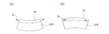
ここで、図8(a)および図8(b)を参照して、基板SUB上に形成された膜RFによる応力と、基板SUBの変形の仕方との関係を説明する。図8(a)に模式的に示すように、膜RFが引張応力Stを有している場合、基板SUBの表面には圧縮応力が作用しているので、基板SUBの表面は凹面を形成するように変形する(反る)。これに対して、図8(b)に示すように、膜RFが圧縮応力Scを有している場合、基板SUBの表面には引張応力が作用しているので、基板SUBの表面は凸面を形成するように変形する。 Here, with reference to FIG. 8A and FIG. 8B, the relationship between the stress caused by the film RF formed on the substrate SUB and the method of deformation of the substrate SUB will be described. As schematically shown in FIG. 8A, when the film RF has a tensile stress St, a compressive stress acts on the surface of the substrate SUB, so that the surface of the substrate SUB forms a concave surface. It deforms (warps). On the other hand, as shown in FIG. 8B, when the film RF has the compressive stress Sc, the surface of the substrate SUB has a convex surface because tensile stress acts on the surface of the substrate SUB. Deform to form.
上述した方法で形成された樹脂層10は引張応力を有するので、図8(a)に示すように、支持基板60は凹面を形成するように変形し、支持基板60の端部は水平面から浮く場合がある。なお、支持基板60の材料や厚さによっては、樹脂層10から圧縮応力が付与されても支持基板60に反りが生じない場合もある。
Since the
次いで、図4(a)および(b)に示すように、樹脂層10の一部上に接着層50を形成する。接着層50は、後述する磁性金属体20の第1開口部25に対応する開口部55を有する。接着層50は、樹脂層10のうち、磁性金属体20の中実部21に対応する領域(第2領域10bとなる領域)全体に形成されてもよいし、その一部に形成されてもよい。好ましくは、樹脂層10のうち第1領域10aとなる部分を包囲するように配置される。
Next, as shown in FIGS. 4A and 4B, an
接着層50は金属層であってもよいし、接着剤で形成されていてもよい。接着層50は樹脂層10の上面に固着されていればよい。例えば、接着層50として、電解めっき、無電解めっきなどの方法で金属層を形成することができる。金属層の材料としては、種々の金属材料を用いることができ、例えば、Ni、Cu、Snを好適に用いることができる。金属層の厚さは、後述する磁性金属体20への溶接工程で耐え得る大きさであればよく、例えば1μm以上100μm以下である。
The
次いで、図5(a)および(b)に示すように、支持基板60上に形成された樹脂層10を、第1開口部25を覆うように磁性金属体20上に固定する。樹脂層10と磁性金属体20とは、接着層50を介して接合される。樹脂層10のうち磁性金属体20の第1開口部25内に位置する領域10aが第1領域、中実部21と重なる領域10bが第2領域となる。
Next, as shown in FIGS. 5A and 5B, the
磁性金属体20は、磁性金属材料から形成され、かつ、少なくとも1つの第1開口部25を有する。磁性金属体20の製造方法は、特に限定しない。例えば、磁性金属板を用意し、フォトリソグラフィプロセスによって、磁性金属板に第1開口部25を形成することによって製造され得る。磁性金属体20の材料としては、例えばインバー(約36wt%のNiを含むFe−Ni系合金)を好適に用いることができる。
The
接着層50が金属層である場合、樹脂層10側からレーザ光を照射し、接着層50を磁性金属体20に溶接してもよい。このとき、間隔を空けて複数箇所でスポット溶接を行ってもよい。スポット溶接を行う箇所の数やその間隔(ピッチ)は適宜選択され得る。このようにして、樹脂層10は、接着層50を介して磁性金属体20に接合される。
When the
なお、接着層50は金属層でなくてもよい。樹脂層10と磁性金属体20とは、接着剤から形成された接着層50を用いて接合されてもよい(ドライラミネートまたは熱ラミネート)。
The
接着層50は、樹脂層10の周縁部のみに配置されていても構わない。磁性金属体20のうち、後で設けられるフレームと重なる部分を「周辺部」、フレームの開口内に位置する部分を「マスク部」とすると、接着層50は、磁性金属体20の周辺部と樹脂層10との間のみに配置されていてもよい。その場合には、マスク部において、磁性金属体20の中実部21と樹脂層10とは接着されない。
The
接着層50は、樹脂層10の第1領域10aとなる部分上には形成されないことが好ましい。第1領域10aに接着層50が形成されていると、後の工程で樹脂層10から支持基板60を剥離した後でも、樹脂層10の引張応力が第1領域10aで面内分布を有してしまう可能性がある。
It is preferable that the
次に、図6(a)および(b)に示すように、例えばレーザアブレーション法により、樹脂層10の第1領域10aに複数の第2開口部13を形成する(レーザ加工工程)。このようにして、磁性金属体20および樹脂層10を含むマスク体30を得る。
Next, as shown in FIGS. 6A and 6B, a plurality of
樹脂層10のレーザ加工には、パルスレーザを用いる。ここでは、YAGレーザを用い、波長が355nm(第3高調波)のレーザ光L1を樹脂層10の所定の領域に照射する。レーザ光L1のエネルギー密度は例えば0.36J/cm2に設定される。前述したように、樹脂層10のレーザ加工は、樹脂層10の表面にレーザ光L1の焦点を合わせて、複数回のショットを行うことによって行われる。ショット周波数は例えば60Hzに設定される。なお、レーザ加工の条件(レーザ光の波長、照射条件など)は、上記に限定されず、樹脂層10を加工し得るように適宜選択される。
A pulse laser is used for laser processing of the
なお、樹脂層10が上述した応力分布を有していると、支持基板60の剥離後に第1領域10a内の応力分布が平均化されたときに、第2開口部13のサイズおよび形状が第1領域10a内の位置に応じて変化する場合がある。このような場合には、支持基板60を剥離した後で第2開口部13が所望のサイズおよび形状を有するように、応力分布の平均化による第2開口部13の変形量を考慮して、第2開口部13を形成しておくことが好ましい。
Note that if the
本実施形態では、支持基板60上に焼成(または乾燥)することによって形成された樹脂層10に対してレーザ加工を行う。支持基板60と樹脂層10との間には気泡が存在しないため、従来よりも高い精度で所望のサイズの第2開口部13を形成することが可能であり、バリ(図27参照)の発生も抑制される。
In the present embodiment, laser processing is performed on the
続いて、図7(a)および(b)に示すように、マスク体30を支持基板60から剥離する。支持基板60の剥離は、例えばレーザリフトオフ法により行うことができる。樹脂層10と支持基板60との密着力が比較的弱い場合には、ナイフエッジなどを用いて機械的に剥離を行ってもよい。
Subsequently, as shown in FIGS. 7A and 7B, the
ここでは、例えばXeClエキシマレーザを用い、支持基板60側からレーザ光(波長:308nm)を照射することによって、樹脂層10を支持基板60から剥離する。なお、レーザ光は、支持基板60を透過し、かつ、樹脂層10で吸収される波長の光であればよく、他のエキシマレーザあるいはYAGレーザなどの高出力レーザを用いてもよい。
Here, for example, an XeCl excimer laser is used, and the
支持基板60を剥離すると、樹脂層10は、内在する引張応力によって、たるみなく(ピンと)張った状態になる。また、樹脂層10のうち磁性金属体20に接合されていない部分(ここでは第1領域10a)内では、所定の方向における引張応力の大きさが平均化され得る。
When the
この後、図示していないが、マスク体30にフレーム40を固定する(フレーム取り付け工程)。このようにして、図1に示す蒸着マスク100が製造される。
Thereafter, although not shown, the
フレーム取り付け工程では、磁性金属体20の周辺部上にフレーム40を載置し、磁性金属体20の周辺部とフレーム40とを接合する。フレーム40は、例えばインバーなどの磁性金属で形成されている。樹脂層10側からレーザ光を照射することによって、磁性金属体20の周辺部とフレーム40とを溶接してもよい(スポット溶接)。スポット溶接のピッチは適宜選択され得る。なお、図1に示す例では、支持基板60の法線方向から見たとき、フレーム40の内縁部と磁性金属体20の内縁部とが略整合しているが、磁性金属体20の一部がフレーム40の内側に露出していてもよい。あるいは、フレーム40は、磁性金属体20の周辺部全体および樹脂層10の一部を覆っていてもよい。
In the frame attaching step, the
前述のように、本実施形態では、樹脂層10および磁性金属体20を所定の層面内方向に引っ張ってフレーム40に固定する工程(架張工程)を行わないので、従来よりも剛性の小さいフレーム40を用いることが可能である。このため、フレーム40は、ABS(アクリロニトリルブタジエンスチレン)、PEEK(ポリエーテルエーテルケトン)などの樹脂から形成されていてもよい。また、マスク体30とフレーム40との接合方法は、レーザ溶接に限定されない。例えば接着剤を用いて磁性金属体20の周辺部とフレーム40とを接合してもよい。
As described above, in the present embodiment, since the step (stretching step) of pulling the
この後、必要に応じて、磁性金属体20を電磁コイルで磁化させる着磁工程を行い、磁性金属体20の残留磁束密度を例えば10mT以上1000mTに調整する。なお、着磁工程を行わなくてもよい。着磁工程を行わなくても、磁性金属体20は磁性体であるので、磁気チャックを用いることにより、蒸着工程において蒸着マスク100をワーク上に保持することができる。
Thereafter, if necessary, a magnetizing step of magnetizing the
上記では、蒸着マスク100を形成する方法を例に説明したが、他の蒸着マスク200、300についても、上記と同様の方法で製造され得る。
In the above description, the method of forming the
<蒸着マスクの他の製造方法>
図3〜図7を参照しながら前述した方法では、樹脂層10と磁性金属体20とを接合した後で、樹脂層10に第2開口部13を形成しているが、樹脂層10と磁性金属体20とを接合する前に、第2開口部13を形成してもよい。また、図3〜図7を参照しながら前述した方法では、マスク体30とフレーム40とを接合する前に、支持基板60をマスク体30から剥離しているが、フレーム40とマスク体30とを接合した後で、支持基板60を剥離してもよい。さらに、樹脂層10と磁性金属体20とを接合させる前に、磁性金属体20にフレーム40を取り付けてもよい。
<Other manufacturing methods of vapor deposition mask>
In the method described above with reference to FIGS. 3 to 7, the
以下、図面を参照しながら、本実施形態の蒸着マスクの他の製造方法を説明する。図面では、図3〜図7と同じ構成要素には同じ参照符号を付している。また、図3〜図7を参照しながら前述した方法と異なる点を中心に説明し、各層の形成方法、材料、厚さ等が上記方法と同様である場合には説明を省略している。 Hereinafter, another method for manufacturing the vapor deposition mask of the present embodiment will be described with reference to the drawings. In the drawing, the same components as those in FIGS. 3 to 7 are denoted by the same reference numerals. Further, the description will be focused on the points different from the method described above with reference to FIGS. 3 to 7, and the description is omitted when the formation method, material, thickness, and the like of each layer are the same as those described above.
図9(a)〜(e)は、蒸着マスクの他の製造方法を例示する工程断面図である。 9A to 9E are process cross-sectional views illustrating another method for manufacturing a vapor deposition mask.
まず、図9(a)に示すように、支持基板60上に樹脂層10を形成する。樹脂層10の形成方法は、図3を参照しながら前述した方法と同様である。ここでは、ポリイミドワニスを支持基板60上に塗布し、焼成することによって樹脂層10を形成する。
First, as shown in FIG. 9A, the
次いで、図9(b)に示すように、レーザ加工により、樹脂層10に第2開口部13を形成する。第2開口部13は、樹脂層10のうち、後の工程で磁性金属体20と接合したときに磁性金属体20の第1開口部25内に位置する領域に形成される。
Next, as shown in FIG. 9B, the
続いて、図9(c)に示すように、接着層50を介して、樹脂層10と磁性金属体20とを接合する。接合方法は、図5を参照しながら前述した方法と同様である。
Subsequently, as illustrated in FIG. 9C, the
この後、図9(d)に示すように、例えばレーザリフトオフ法により、樹脂層10から支持基板60を剥離する。
Thereafter, as shown in FIG. 9D, the
次いで、図9(e)に示すように、例えばレーザ光L2を用いてスポット溶接を行うことにより、フレーム40を磁性金属体20の周辺部に設ける。このようにして、蒸着マスク100を得る。
Next, as shown in FIG. 9E, the
図10(a)〜(e)は、蒸着マスクの他の製造方法を例示する工程断面図である。 10A to 10E are process cross-sectional views illustrating another method for manufacturing a vapor deposition mask.
まず、図10(a)に示すように、支持基板60上に樹脂層10を形成する。樹脂層10の形成方法は、図3を参照しながら前述した方法と同様である。
First, as shown in FIG. 10A, the
次いで、図10(b)に示すように、接着層50を介して、樹脂層10と磁性金属体20とを接合する。
Next, as shown in FIG. 10B, the
続いて、図10(c)に示すように、レーザ加工により、樹脂層10に第2開口部13を形成する。
Subsequently, as shown in FIG. 10C, the
この後、図10(d)に示すように、例えばレーザ光L2を用いてスポット溶接を行うことにより、フレーム40を磁性金属体20の周辺部に設ける。
Thereafter, as shown in FIG. 10D, the
次いで、図10(e)に示すように、例えばレーザリフトオフ法により、樹脂層10から支持基板60を剥離する。このようにして、蒸着マスク100を得る。
Next, as shown in FIG. 10E, the
図11(a)〜(e)は、蒸着マスクのさらに他の製造方法を例示する工程断面図である。 11A to 11E are process cross-sectional views illustrating still another method for manufacturing a vapor deposition mask.
まず、図11(a)に示すように、支持基板60上に樹脂層10を形成する。樹脂層10の形成方法は、図3を参照しながら前述した方法と同様である。
First, as shown in FIG. 11A, the
また、図11(b)に示すように、フレーム40に磁性金属体20を取り付けることにより、フレーム構造体を形成する。具体的には、磁性金属体20の周辺部上にフレーム40を載置し、周辺部とフレーム40とを接合する。ここでは、磁性金属体20側からレーザ光L3を照射することによって、磁性金属体20の周辺部とフレーム40とを溶接する。例えば、所定の間隔を空けて複数箇所でスポット溶接を行ってもよい。なお、架張溶接装置を用いて、磁性金属体20に所定の方向に一定の張力を付与した状態で、磁性金属体20をフレーム40に接合してもよい。ただし、本実施形態では、磁性金属体20はフレーム40に固定されていればよいので、大きな張力を付与する必要はない。
Further, as shown in FIG. 11B, the frame structure is formed by attaching the
続いて、図11(c)に示すように、接着層50を介して、樹脂層10と磁性金属体20とを接合する。
Subsequently, as illustrated in FIG. 11C, the
次いで、図11(d)に示すように、レーザ加工により、樹脂層10に第2開口部13を形成する。
Next, as shown in FIG. 11D, the
この後、図11(e)に示すように、例えばレーザリフトオフ法により、樹脂層10から支持基板60を剥離する。このようにして、蒸着マスク100を得る。
Thereafter, as shown in FIG. 11E, the
このように、本実施形態の蒸着マスク100は種々の方法で製造され得る。なお、図9に例示した方法では、第2開口部13を形成した樹脂層10と磁性金属体20とを接合する際に、高精度な位置合わせを行う必要がある。これに対し、樹脂層10と磁性金属体20とを接合した後に第2開口部13を形成すると、そのような高精度な位置合わせを行わなくてもよいので有利である。
Thus, the
また、図10および図11に例示した方法では、支持基板60を剥離する前に、フレーム40の取り付けを行う。この場合、重量および嵩の大きいフレーム40が取り付けられた支持基板60を、レーザリフトオフ装置のステージに設置し、支持基板60の剥離を行うため、他の方法よりも、使用するレーザリフトオフ装置のステージを大きく、かつ、高強度にする必要がある。また、レーザヘッドとステージとの距離WD(ワークディスタンス)を大きくする必要がある。これに対し、支持基板60の剥離後に、フレーム40の取り付け工程を行うと、レーザリフトオフ装置のステージの大きさ、強度、WDなどに上記のような制限が課せられないため、より実用的である。
In the method illustrated in FIGS. 10 and 11, the
<本実施形態の製造方法による効果>
本実施形態の蒸着マスクの製造方法によると、樹脂材料を含む溶液または樹脂材料の前駆体を含む溶液を支持基板60の表面に付与し、熱処理を行うことによって樹脂層10を形成する。この方法で形成された樹脂層10は、支持基板60に密着しており、樹脂層10と支持基板60との界面に気泡は生じない。従って、支持基板60上で樹脂層10に複数の第2開口部13を形成することにより、所望のサイズの第2開口部13を従来よりも高い精度で形成でき、なおかつ、バリ98(図27参照)の発生を抑制できる。
<Effects of the manufacturing method of the present embodiment>
According to the vapor deposition mask manufacturing method of this embodiment, the
また、本実施形態によると、樹脂層10に所望の引張応力を生じさせることができる。これにより、樹脂層10の第1領域10aに生じるたわみ量を低減できる。このため、第1領域10a上に、第2開口部13に近接して磁性金属を配置しなくても、蒸着対象基板上に樹脂層10を密着させることが可能になる。従って、第1開口部25のサイズを拡大でき、例えばオープンマスクの使用も可能になる。中実部の面積率の極端に小さい(例えば、マスク部の面積に対して50%以下)磁性金属体20を使用することも可能である。また、高精度にパターニングされた磁性金属層を形成しなくてもよいので、製造工程を簡略化できる。さらに、熱膨張係数αMの大きい金属材料を使用することも可能になる。従って、磁性金属体20の形状および金属材料の選択の自由度を従来よりも高めることができる。
Further, according to the present embodiment, a desired tensile stress can be generated in the
本実施形態では、支持基板60上で樹脂層10を形成し、支持基板60に支持された状態の樹脂層10と磁性金属体20とを接合する。樹脂層10は残留応力として所定の引張応力を有しているので、樹脂層10を引っ張ってフレームに接合させる架張工程を行わない。大掛かりな架張機を用いた架張工程が不要になるので、製造コストを低減できるメリットがある。また、架張工程を行わないので、フレーム40から磁性金属体20に所定の層面内方向の張力が付与されない。従って、従来よりもフレーム40の剛性を小さくすることが可能になり、フレーム40の材料選択の自由度、および、フレーム幅、厚さ等の設計の自由度が大きくなる。
In the present embodiment, the
特許文献1などに記載の従来方法では、架張工程によって樹脂フィルムをフレームに固定した後で、樹脂フィルムに対するレーザ加工が行われる。これに対し、本実施形態では、フレーム40の取り付け工程は、樹脂層10のレーザ加工前に行ってもよいし、レーザ加工後に行ってもよい。レーザ加工後にフレーム40の取り付け工程を行う場合には、次のようなメリットがある。フレーム40が取り付けられる前の、支持基板60によって支持されたマスク体30(レーザ加工前のマスク体を含む)は、フレーム40が取り付けられた後のマスク体30よりも軽量で取り扱いやすいので、レーザ加工機への設置、搬送等の作業が容易になる。また、フレーム40が取り付けられていないので、樹脂層10にレーザ光L1を照射しやすく、樹脂層10を加工し易い。さらに、特許文献1の方法では、樹脂層のレーザ加工がうまくいかなかったときに、フレームから積層マスクを剥離する必要があるが、フレーム40を取り付ける前にレーザ加工を行う場合には、そのような剥離工程は不要である。
In the conventional method described in
さらに、架張工程によってフレームに固定された樹脂フィルムは、湿度や温度などの周囲環境の変化に敏感であり、樹脂フィルムのたわみ量は周囲環境によって変化し得る。これに対し、本実施形態では、樹脂層10のたわみはゼロまたは僅かであり、たわみ量の経時変化もほとんど見られない。
Furthermore, the resin film fixed to the frame by the stretching process is sensitive to changes in the surrounding environment such as humidity and temperature, and the amount of deflection of the resin film can vary depending on the surrounding environment. On the other hand, in the present embodiment, the deflection of the
ところで、蒸着工程における蒸着マスクの温度上昇の大きさ、すなわち、製造時の蒸着マスクの温度T1と、蒸着工程における蒸着マスクの温度T2との差ΔT(℃)(=T2−T1)は、蒸着方法、蒸着装置等によって変わる。温度差ΔTが比較的小さく抑えられる場合、ΔTは3℃未満、例えば1℃程度である。一方、ΔTは3℃〜15℃程度になることもある。なお、本実施形態における製造時の温度T1は、製造装置(例えば、樹脂層10の加工に使用するレーザ加工機、フレーム取り付け工程に使用する溶接機など)が設置されている環境温度であり、例えば室温である。蒸着工程における温度T2は、蒸着源の位置をワークに対して相対的に移動させながら(走査しながら)蒸着を行う場合には、蒸着マスクのうち、蒸着が行われている部分の温度を指す。本実施形態では、ΔTが比較的大きい場合(例えば3℃超)、必要に応じて、次の方法で、位置ずれを抑制することが可能である。まず、蒸着マスクの温度上昇(ΔT)を予め測定する。次いで、ΔTの測定結果に基づいて、熱膨張によって発生する位置ずれ量を算出する。位置ずれ量は、第2開口部13の位置と蒸着位置とのずれ、および、第2開口部13自体の変形による第2開口部13の形状と所望の蒸着パターンとのずれを含む。この位置ずれ量を相殺するように、樹脂層10の第2開口部13のサイズを所望の蒸着パターンよりも所定量だけ小さく形成する。なお、位置ずれ量を算出する代わりに、実際に蒸着を行って位置ずれ量を測定してもよい。
By the way, the magnitude of the temperature rise of the vapor deposition mask in the vapor deposition process, that is, the difference ΔT (° C.) (= T2−T1) between the temperature T1 of the vapor deposition mask at the time of manufacture and the temperature T2 of the vapor deposition mask in the vapor deposition process. It depends on the method, vapor deposition equipment, etc. When the temperature difference ΔT is kept relatively small, ΔT is less than 3 ° C., for example, about 1 ° C. On the other hand, ΔT may be about 3 ° C. to 15 ° C. In addition, the temperature T1 at the time of manufacture in the present embodiment is an environmental temperature in which a manufacturing apparatus (for example, a laser processing machine used for processing the
(熱処理条件と樹脂層の引張応力との関係)
本発明者は、樹脂層の形成条件(熱処理条件)と、樹脂層の引張応力および樹脂層のたわみ量との関係を検討した。以下、その方法および結果を説明する。
(Relationship between heat treatment conditions and tensile stress of resin layer)
This inventor examined the relationship between the resin layer formation conditions (heat treatment conditions), the tensile stress of the resin layer, and the amount of deflection of the resin layer. Hereinafter, the method and result will be described.
・サンプルA〜Cの作製方法
熱処理条件を異ならせて、ガラス基板61上にポリイミド膜62を形成し、サンプルA〜Cを得た。図12は、サンプルA〜Cの上面図である。
-Preparation method of samples A-C The heat treatment conditions were varied, the
まず、支持基板として、ガラス基板(旭硝子製AN−100)61を用意した。ガラス基板61の熱膨張係数は3.8ppm/℃、サイズは370mm×470mm、厚さは0.5mmであった。
First, a glass substrate (AN-100 manufactured by Asahi Glass) 61 was prepared as a support substrate. The
上記のガラス基板61の一部上に、ポリイミドワニス(宇部興産株式会社製U−ワニス−S)を塗布した。ここでは、図12に示すように、ガラス基板61における所定の領域(330mm×366mm)にポリイミドワニスを塗布した。
A polyimide varnish (U-Varnish-S manufactured by Ube Industries, Ltd.) was applied on a part of the
次いで、ポリイミドワニスを塗布したガラス基板61に対して、圧力:20Paの真空雰囲気下で熱処理を行い、ポリイミド膜62を形成した。熱処理では、室温(ここでは25℃とした)から500℃(最高温度)まで昇温し、500℃で所定の時間保持した。この後、パージガスとして窒素ガスを供給し、次いで急冷(3分間)した。各サンプルにおける500℃までの昇温時間、500℃での保持時間、昇温速度(室温から500℃到達時まで)、およびポリイミド膜62の厚さを表1に示す。
Next, the
このようにして、サンプルA〜Cとして、ポリイミド膜62が形成されたガラス基板61を得た。サンプルA〜Cでは、ポリイミド膜62の引張応力によって、ガラス基板61に圧縮応力が付与され、ガラス基板61に反りが生じた。長辺方向および短辺方向におけるガラス基板61の反り量の平均値を表1に示す。
Thus, the
・ポリイミド膜62の引張応力の算出
次いで、サンプルA〜Cにおけるガラス基板61の反り量から、ポリイミド膜62の引張応力を算出した。結果を表1に示す。引張応力は、Stoneyの式を用いて、ガラス基板61の厚さ、ヤング率、ポアソン比、ポリイミド膜62の厚さ、ガラス基板61の反りの曲率半径(近似値)から求めることができる。
Calculation of tensile stress of
また、表1には、比較のため、昇温速度の小さい条件でポリイミド膜を作製した場合の結果も示す(「サンプルD」とする)。表1に示すように、サンプルDでは、120℃、150℃、180℃に到達後、その温度で所定時間保持することにより、段階的に450℃まで昇温した。サンプルDの引張応力は、ガラス基板61の反りを10μmとして算出した値である。
For comparison, Table 1 also shows the results when a polyimide film was produced under conditions with a low rate of temperature increase (referred to as “sample D”). As shown in Table 1, in Sample D, after reaching 120 ° C., 150 ° C., and 180 ° C., the temperature was raised to 450 ° C. stepwise by holding at that temperature for a predetermined time. The tensile stress of sample D is a value calculated by setting the warp of the

さらに、同じ熱処理条件で6つのサンプルB1〜B6を作製し、ポリイミド膜62に生じた引張応力を算出した。サンプルB1〜B6の熱処理条件は、サンプルBと同様とした(室温〜500℃、圧力:20Pa、加熱時間:13分(昇温8分+保持5分)、昇温速度:59℃/分)。ただし、熱処理前に、ポリイミドワニスが付与されたガラス基板61が設置されたチャンバーを減圧する速度をサンプルBよりも小さくした。これらのサンプルについても、上記と同様に、ガラス基板の反り量からポリイミド膜の引張応力を求めた。結果を表2に示す。
Furthermore, six samples B1 to B6 were produced under the same heat treatment conditions, and the tensile stress generated in the
上記の結果から、熱処理条件によって、支持基板上の樹脂層に生じる引張応力を制御できることが確認された。例えば、昇温速度を大きくすることで、引張応力の大きい樹脂層を形成できることが分かった。なお、ここでは、サンプルごとに昇温速度を変えて熱処理を行ったが、昇温速度以外の熱処理条件を変えても、樹脂層の引張応力の大きさを異ならせることができる。 From the above results, it was confirmed that the tensile stress generated in the resin layer on the support substrate can be controlled by the heat treatment conditions. For example, it was found that a resin layer having a large tensile stress can be formed by increasing the temperature rising rate. Here, the heat treatment was performed by changing the heating rate for each sample, but the tensile stress of the resin layer can be varied even if the heat treatment conditions other than the heating rate are changed.
(実施例)
実施例の蒸着マスクを作製し、樹脂層のたわみ量を評価したので、その結果を説明する。
(Example)
The vapor deposition mask of an Example was produced and the deflection amount of the resin layer was evaluated, The result is demonstrated.
図13(a)は、実施例1の蒸着マスクを説明するための平面図であり、図13(b)は、図13(a)のB−B線に沿った断面図である。実施例1の蒸着マスクの作製方法は、図11を参照しながら前述した方法と同様とした。 Fig.13 (a) is a top view for demonstrating the vapor deposition mask of Example 1, FIG.13 (b) is sectional drawing along the BB line of Fig.13 (a). The manufacturing method of the vapor deposition mask of Example 1 was the same as that described above with reference to FIG.
・実施例1の蒸着マスクの作製
実施例1では、支持基板として、ガラス基板(200×130mm、厚さ:0.5mm)を用いた。ガラス基板上に、上記のサンプルBと同様の熱処理条件で、ポリイミド膜(厚さ:20μm)71を形成した。
-Preparation of the vapor deposition mask of Example 1 In Example 1, the glass substrate (200x130 mm, thickness: 0.5 mm) was used as a support substrate. A polyimide film (thickness: 20 μm) 71 was formed on the glass substrate under the same heat treatment conditions as in Sample B above.
また、磁性金属体として、3つの第1開口部(50mm×90mm)73を有するオープンマスク(200×110mm、厚さ:100μm)72を用意した。このオープンマスク72を、不図示のSUS製のフレーム(200×130mm、厚さ:10mm、フレーム幅20mm)に溶接した。
Moreover, an open mask (200 × 110 mm, thickness: 100 μm) 72 having three first openings (50 mm × 90 mm) 73 was prepared as a magnetic metal body. This
次いで、ガラス基板上のポリイミド膜71の一部上に、接着層として、エポキシ樹脂系の接着剤(セメダイン社製EP330)75を付与した。この後、接着剤75を介して、ポリイミド膜71とオープンマスク72とを接合した。
Next, an epoxy resin-based adhesive (EP330 manufactured by Cemedine) 75 was applied as an adhesive layer on part of the
続いて、ポリイミド膜71から支持基板を剥離した。ポリイミド膜71には第2開口部は設けなかった。このようにして、実施例1の蒸着マスクを得た。
Subsequently, the support substrate was peeled from the
実施例1の蒸着マスクは、3つのセルC1〜C3を含んでいる。ここで「セル」とは、蒸着マスクを法線方向から見たとき、各第1開口部73およびその周辺を含む部分を指し、上述した単位領域Uに対応する。また、各セルにおいて、ポリイミド膜71のうち第1開口部73によって露出する領域71aを「第1領域」、オープンマスク72と接着剤75によって接合された領域71bを「第2領域」とする。
The vapor deposition mask of Example 1 includes three cells C1 to C3. Here, the “cell” refers to a portion including each
・実施例2の蒸着マスクの作製
上記のサンプルDと同様の熱処理条件でポリイミド膜71を形成した点以外は、実施例1と同様の方法で実施例2の蒸着マスクを作製した。ただし、実施例2では、オープンマスク72の3つの第1開口部73のうち中央に位置する開口部にはポリイミド膜71を貼らなかった。従って、実施例2の蒸着マスクは2つのセルを含む。
-Preparation of the vapor deposition mask of Example 2 The vapor deposition mask of Example 2 was produced by the method similar to Example 1 except the point which formed the
・実施例1、2の蒸着マスクの観察
実施例1および実施例2の蒸着マスクの写真を、図23(a)および(b)に示す。実施例1の蒸着マスクでは、ポリイミド膜71のたわみに依存した皺は見られない。また、ポリイミド膜71は膜応力の分布に依存したように思われる模様が観察される。一方、実施例2の蒸着マスクでは、ポリイミド膜71のたわみに依存した皺が見られ、セルの中央部でたわみが大きくなっていることが分かる。
-Observation of the vapor deposition mask of Example 1, 2 The photograph of the vapor deposition mask of Example 1 and Example 2 is shown to Fig.23 (a) and (b). In the vapor deposition mask of Example 1, no wrinkles depending on the deflection of the
・ポリイミド膜71のたわみ測定
実施例1の蒸着マスクのセルC1〜C3のそれぞれについて、ポリイミド膜71のたわみの測定を行った。
-Deflection measurement of
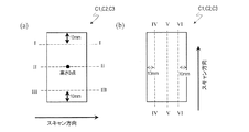
図14(a)および(b)は、それぞれ、たわみ測定における、各セルのスキャン方向を示す平面図である。ここでは、レーザ変位計(キーエンス社製、LK−H057K)を用いて、各セルにおける第1開口部73の短辺方向および長辺方向にスキャンして、ポリイミド膜71の高さの変化を調べた。データサンプリング周期を200μsとした。
FIGS. 14A and 14B are plan views showing the scan direction of each cell in the deflection measurement. Here, using a laser displacement meter (manufactured by Keyence Corporation, LK-H057K), scanning is performed in the short side direction and the long side direction of the
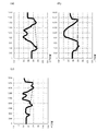
図15〜図20は、実施例1の蒸着マスクにおける各セルのポリイミド膜71の測定結果を示す図である。
15-20 is a figure which shows the measurement result of the
図15(a)〜(c)および図16(a)〜(c)は、それぞれ、実施例1の蒸着マスクにおけるセルC1のポリイミド膜71の高さの変化を示す図である。同様に、図17(a)〜(c)および図18(a)〜(c)は、それぞれ、セルC2のポリイミド膜71の高さの変化を示す図であり、図19(a)〜(c)および図20(a)〜(c)は、それぞれ、セルC3のポリイミド膜71の高さの変化を示す図である。また、図15、図17、図19の(a)〜(c)は、それぞれ、図14(a)に示すI−I、II−II、III−III線に沿って、セルの短手方向にポリイミド膜71をスキャンしたときの測定結果を示す。図16、図18、図20の(a)〜(c)は、それぞれ、図14(a)に示すIV−IV、V−V、VI−VI線に沿って、セルの長手方向にポリイミド膜71をスキャンしたときの測定結果を示す。
FIGS. 15A to 15C and FIGS. 16A to 16C are diagrams showing changes in the height of the
これらの図において、縦軸はポリイミド膜71の高さであり、各セルの中央部の高さを基準とした値である。横軸は、200μs間隔で取得したデータ点数である。なお、手動でセンサーを移動させて測定しており、センサーのスキャン速度が一定でないため、横軸は距離とは対応していない。
In these figures, the vertical axis represents the height of the
図15〜図20において、ポリイミド膜71の第1領域71aの高さが傾きを有しているが、この傾きは、フレームのチルト、接着剤75の厚さばらつき等に依存する。また、ポリイミド膜71の第1領域71aと第2領域71bとの間に段差hが生じている。これは、実施例1の蒸着マスクを、ポリイミド膜71を上にして設置し、下方(ポリイミド膜71のオープンマスク72側)から変位計で測定を行っているからである。段差hはオープンマスク72および接着剤75の合計厚さに対応する。
15 to 20, the height of the
セルC1〜C3の各断面の測定結果に補正線を破線で示す。「補正線」は、ポリイミド膜71のたわみがゼロの場合のポリイミド膜71(第1領域71a)の高さの変化を表す。ポリイミド膜71にたわみが生じていると、ポリイミド膜71の高さの実測値は、補正線の高さよりも小さくなる。ここでは、各断面におけるポリイミド膜71のたわみ量として、補正線と実測値との高さの差(補正線の高さに対して実測値がマイナスになる場合)の最大値を求めた。また、たわみ量の最大値を、そのセルの「最大たわみ量」とした。
Correction lines are indicated by broken lines in the measurement results of the cross sections of the cells C1 to C3. The “correction line” represents a change in the height of the polyimide film 71 (
この結果、いずれのセルにおいても、最大たわみ量は5μm以下であった。従って、実施例1の蒸着マスクでは、セルの位置にかかわらず、ポリイミド膜71の第1領域71aは所定の大きさの引張応力を有しており、たわみ量(すなわち実測値と補正線との高さの差)を抑制できることが分かった。また、ポリイミド膜71の第1領域71a内では、熱処理直後に生じた応力分布が小さくなる(平均化される)ことが分かった。
As a result, in all the cells, the maximum deflection amount was 5 μm or less. Therefore, in the vapor deposition mask of Example 1, regardless of the position of the cell, the
一方、実施例2の蒸着マスクのセルについても、実施例1と同様の方法で、ポリイミド膜71のたわみ測定を行い、最大たわみ量を求めた。
On the other hand, with respect to the cell of the vapor deposition mask of Example 2, the deflection of the
図21(a)〜(c)および図22(a)〜(c)は、それぞれ、実施例2の蒸着マスクにおける1つのセルのポリイミド膜71の高さの変化を示し、図14(a)および(b)に示すI−I、II−II、III−III、IV−IV、V−V、VI−VI線に沿ってポリイミド膜71をスキャンしたときの測定結果を示す。
FIGS. 21A to 21C and FIGS. 22A to 22C respectively show changes in the height of the
この結果、実施例2の蒸着マスクでは、各セルにおける最大たわみ量は400μm以上500μm以下であり、実施例1よりも大きなたわみが生じていることが分かった。従って、ポリイミド膜71の引張応力を大きくすることにより、ポリイミド膜71のたわみ量を低減できることが確認された。
As a result, in the vapor deposition mask of Example 2, the maximum deflection amount in each cell was 400 μm or more and 500 μm or less, and it was found that a larger deflection than that in Example 1 occurred. Therefore, it was confirmed that the amount of deflection of the
なお、所定の引張応力(例えば3MPa以上)を有する樹脂膜と、引張応力が比較的小さくなるような条件で形成された従来の樹脂膜とは、支持基板または磁性金属体にかかる圧縮応力(反り量)の測定、樹脂膜の面内配向(IR吸収スペクトル)の測定などによって区別され得る。例えば、従来の樹脂膜では、表面および裏面のIR吸収スペクトルは略同じであるが、引張応力の大きい樹脂膜では、表面および裏面のIR吸収スペクトルが異なる等の違いが生じ得る。また、オープンマスクに接合された所定の引張応力を有する樹脂膜と、架張によってフレームに固定された従来の樹脂膜とは、例えば偏光を用いた観察によっても区別され得る。 Note that a resin film having a predetermined tensile stress (for example, 3 MPa or more) and a conventional resin film formed under a condition that the tensile stress is relatively small are a compressive stress (warpage) applied to the support substrate or the magnetic metal body. For example, the measurement of the in-plane orientation (IR absorption spectrum) of the resin film. For example, in the conventional resin film, the IR absorption spectra on the front surface and the back surface are substantially the same, but in the resin film having a large tensile stress, differences such as different IR absorption spectra on the front surface and the back surface may occur. Further, a resin film having a predetermined tensile stress bonded to an open mask and a conventional resin film fixed to a frame by stretching can be distinguished from each other by observation using polarized light, for example.
(有機半導体素子の製造方法)
本発明の実施形態による蒸着マスクは、有機半導体素子の製造方法における蒸着工程に好適に用いられる。
(Method for manufacturing organic semiconductor element)
The vapor deposition mask by embodiment of this invention is used suitably for the vapor deposition process in the manufacturing method of an organic-semiconductor element.
以下、有機EL表示装置の製造方法を例として説明を行う。 Hereinafter, the manufacturing method of the organic EL display device will be described as an example.
図24は、トップエミッション方式の有機EL表示装置500を模式的に示す断面図である。
FIG. 24 is a cross-sectional view schematically showing a top emission type organic
図24に示すように、有機EL表示装置500は、アクティブマトリクス基板(TFT基板)510および封止基板520を備え、赤画素Pr、緑画素Pgおよび青画素Pbを有する。
As shown in FIG. 24, the organic
TFT基板510は、絶縁基板と、絶縁基板上に形成されたTFT回路とを含む(いずれも不図示)。TFT回路を覆うように、平坦化膜511が設けられている。平坦化膜511は、有機絶縁材料から形成されている。
The
平坦化膜511上に、下部電極512R、512Gおよび512Bが設けられている。下部電極512R、512Gおよび512Bは、赤画素Pr、緑画素Pgおよび青画素Pbにそれぞれ形成されている。下部電極512R、512Gおよび512Bは、TFT回路に接続されており、陽極として機能する。隣接する画素間に、下部電極512R、512Gおよび512Bの端部を覆うバンク513が設けられている。バンク513は、絶縁材料から形成されている。
On the
赤画素Pr、緑画素Pgおよび青画素Pbの下部電極512R、512Gおよび512B上に、有機EL層514R、514Gおよび514Bがそれぞれ設けられている。有機EL層514R、514Gおよび514Bのそれぞれは、有機半導体材料から形成された複数の層を含む積層構造を有する。この積層構造は、例えば、下部電極512R、512Gおよび512B側から、ホール注入層、ホール輸送層、発光層、電子輸送層および電子注入層をこの順で含んでいる。赤画素Prの有機EL層514Rは、赤色光を発する発光層を含む。緑画素Pgの有機EL層514Gは、緑色光を発する発光層を含む。青画素Pbの有機EL層514Bは、青色光を発する発光層を含む。
Organic EL layers 514R, 514G, and 514B are provided on the
有機EL層514R、514Gおよび514B上に、上部電極515が設けられている。上部電極515は、透明導電材料を用いて表示領域全体にわたって連続するように(つまり赤画素Pr、緑画素Pgおよび青画素Pbに共通に)形成されており、陰極として機能する。上部電極515上に、保護層516が設けられている。保護層516は、有機絶縁材料から形成されている。
An
TFT基板510の上述した構造は、TFT基板510に対して透明樹脂層517によって接着された封止基板520によって封止されている。
The above-described structure of the
有機EL表示装置500は、本発明の実施形態による蒸着マスクを用いて以下のようにして製造され得る。図25(a)〜(d)および図26(a)〜(d)は、有機EL表示装置500の製造工程を示す工程断面図である。なお、以下では、赤画素用の蒸着マスク101R、緑画素用の蒸着マスク101G、青画素用の蒸着マスク101Bを順に用いてワーク上に有機半導体材料を蒸着する(TFT基板510上に有機EL層514R、514Gおよび514Bを形成する)工程を中心に説明を行う。
The organic
まず、図25(a)に示すように、絶縁基板上に、TFT回路、平坦化膜511、下部電極512R、512G、512Bおよびバンク513が形成されたTFT基板510を用意する。TFT回路、平坦化膜511、下部電極512R、512G、512Bおよびバンク513を形成する工程は、公知の種々の方法により実行され得る。
First, as shown in FIG. 25A, a
次に、図25(b)に示すように、真空蒸着装置内に保持された蒸着マスク101Rに、搬送装置によりTFT基板510を近接させて配置する。このとき、樹脂層10の第2開口部13Rが赤画素Prの下部電極512Rに重なるように、蒸着マスク101RとTFT基板510とが位置合わせされる。また、TFT基板510に対して蒸着マスク101Rとは反対側に配置された不図示の磁気チャックにより、蒸着マスク101RをTFT基板510に対して密着させる。
Next, as shown in FIG. 25 (b), the
続いて、図25(c)に示すように、真空蒸着により、赤画素Prの下部電極512R上に、有機半導体材料を順次堆積し、赤色光を発する発光層を含む有機EL層514Rを形成する。
Subsequently, as shown in FIG. 25C, an organic semiconductor material is sequentially deposited on the
次に、図25(d)に示すように、蒸着マスク101Rに代えて、蒸着マスク101Gを真空蒸着装置内に設置する。樹脂層10の第2開口部13Gが緑画素Pgの下部電極512Gに重なるように、蒸着マスク101GとTFT基板510との位置合わせを行う。また、磁気チャックにより、蒸着マスク101GをTFT基板510に対して密着させる。
Next, as shown in FIG. 25D, instead of the vapor deposition mask 101R, the vapor deposition mask 101G is installed in a vacuum vapor deposition apparatus. The vapor deposition mask 101G and the
続いて、図26(a)に示すように、真空蒸着により、緑画素Pgの下部電極512G上に、有機半導体材料を順次堆積し、緑色光を発する発光層を含む有機EL層514Gを形成する。
Subsequently, as shown in FIG. 26A, organic semiconductor materials are sequentially deposited on the
次に、図26(b)に示すように、蒸着マスク101Gに代えて、蒸着マスク101Bを真空蒸着装置内に設置する。樹脂層10の第2開口部13Bが青画素Pbの下部電極512Bに重なるように、蒸着マスク101BとTFT基板510との位置合わせを行う。また、磁気チャックにより、蒸着マスク101BをTFT基板510に対して密着させる。
Next, as shown in FIG. 26B, a vapor deposition mask 101B is placed in a vacuum vapor deposition apparatus in place of the vapor deposition mask 101G. The vapor deposition mask 101B and the
続いて、図26(c)に示すように、真空蒸着により、青画素Pbの下部電極512B上に、有機半導体材料を順次堆積し、青色光を発する発光層を含む有機EL層514Bを形成する。
Subsequently, as shown in FIG. 26C, an organic semiconductor material is sequentially deposited on the
次に、図26(d)に示すように、有機EL層514R、514Gおよび514B上に、上部電極515および保護層516を順次形成する。上部電極515および保護層516の形成は、公知の種々の方法により実行され得る。このようにして、TFT基板510が得られる。
Next, as shown in FIG. 26D, the
その後、TFT基板510に対して封止基板520を透明樹脂層517により接着することにより、図24に示した有機EL表示装置500が完成する。
Thereafter, the sealing
なお、ここでは、赤画素Pr、緑画素Pgおよび青画素Pbの有機EL層514R、514Gおよび514Bにそれぞれ対応する3枚の蒸着マスク101R、101G、101Bを用いたが、1枚の蒸着マスクを順次ずらすことによって、赤画素Pr、緑画素Pgおよび青画素Pbに対応する有機EL層514R、514Gおよび514Bを形成してもよい。また、有機EL表示装置500において、封止基板520に代えて封止フィルムを用いてもよい。あるいは、封止基板(または封止フィルム)を使用せずに、TFT基板510に薄膜封止(TFE:Thin Film Encapsulation)構造を設けてもよい。薄膜封止構造は、例えば、窒化シリコン膜などの複数の無機絶縁膜を含む。薄膜封止構造は有機絶縁膜をさらに含んでもよい。
In this example, three vapor deposition masks 101R, 101G, and 101B corresponding to the organic EL layers 514R, 514G, and 514B of the red pixel Pr, the green pixel Pg, and the blue pixel Pb are used, respectively. The organic EL layers 514R, 514G, and 514B corresponding to the red pixel Pr, the green pixel Pg, and the blue pixel Pb may be formed by sequentially shifting. In the organic
なお、上記の説明では、トップエミッション方式の有機EL表示装置500を例示したが、本実施形態の蒸着マスクがボトムエミッション方式の有機EL表示装置の製造にも用いられることはいうまでもない。
In the above description, the top emission type organic
また、本実施形態の蒸着マスクを用いて製造される有機EL表示装置は、必ずしもリジッドなデバイスでなくてもよい。本実施形態の蒸着マスクは、フレキシブルな有機EL表示装置の製造にも好適に用いられる。フレキシブルな有機EL表示装置の製造方法においては、支持基板(例えばガラス基板)上に形成されたポリマ層(例えばポリイミド層)上に、TFT回路などが形成され、保護層の形成後にポリマ層がその上の積層構造ごと支持基板から剥離(例えばレーザリフトオフ法が用いられる)される。 Moreover, the organic EL display device manufactured using the vapor deposition mask of this embodiment does not necessarily need to be a rigid device. The vapor deposition mask of this embodiment is also suitably used for manufacturing a flexible organic EL display device. In a method for manufacturing a flexible organic EL display device, a TFT circuit or the like is formed on a polymer layer (for example, a polyimide layer) formed on a support substrate (for example, a glass substrate), and the polymer layer is formed after the protective layer is formed. The entire laminated structure is peeled off from the support substrate (for example, a laser lift-off method is used).
また、本実施形態の蒸着マスクは、有機EL表示装置以外の有機半導体素子の製造にも用いられ、特に、高精細な蒸着パターンの形成が必要とされる有機半導体素子の製造に好適に用いられる。 Moreover, the vapor deposition mask of this embodiment is used also for manufacture of organic-semiconductor elements other than an organic electroluminescent display apparatus, and is used suitably especially for manufacture of the organic-semiconductor element which needs formation of a high-definition vapor deposition pattern. .
本発明の実施形態による蒸着マスクは、有機EL表示装置をはじめとする有機半導体素子の製造に好適に用いられ、高精細な蒸着パターンの形成が必要とされる有機半導体素子の製造に特に好適に用いられる。 The vapor deposition mask according to the embodiment of the present invention is preferably used for manufacturing an organic semiconductor element such as an organic EL display device, and particularly suitable for manufacturing an organic semiconductor element that requires formation of a high-definition vapor deposition pattern. Used.
10 樹脂層
10a 第1領域
10b 第2領域
13 開口部
20 磁性金属体
21 中実部
25 開口部
30 マスク体
40 フレーム
50 接着層
60 支持基板
L1、L1、L3 レーザ光
100、200、300 蒸着マスク
500 有機EL表示装置
510 TFT基板
511 平坦化膜
512B、512G、512R 下部電極
513 バンク
514B、514G、514R 有機EL層
515 上部電極
516 保護層
517 透明樹脂層
520 封止基板
Pb 青画素
Pg 緑画素
Pr 赤画素
U 単位領域
DESCRIPTION OF
Claims (14)
(A)少なくとも1つの第1開口部を有する磁性金属体を用意する工程と、
(B)基板を用意する工程と、
(C)前記基板の表面に樹脂材料を含む溶液または樹脂材料のワニスを付与した後、熱処理を行うことによって樹脂層を形成する工程と、
(D)前記工程(A)、前記工程(B)および前記工程(C)の後、前記基板に形成された前記樹脂層を、前記磁性金属体上に、前記少なくとも1つの第1開口部を覆うように固定する工程であって、
(D1)前記樹脂層の一部上に、めっきによって金属層を形成する工程と、
(D2)前記金属層を介して、前記樹脂層を前記磁性金属体に接合する工程と
を含み、
前記金属層は、前記樹脂層のうち前記少なくとも1つの第1開口部内に位置する領域には形成されておらず、かつ、前記樹脂層のうち前記少なくとも1つの第1開口部内に位置する領域には磁性金属は存在していない、工程と、
(E)前記樹脂層に、複数の第2開口部を形成する工程と、
(F)前記工程(D)および前記工程(E)の後、前記樹脂層から前記基板を剥離する工程と
を包含する、蒸着マスクの製造方法。 A method for producing a vapor deposition mask comprising a resin layer and a magnetic metal body formed on the resin layer,
(A) preparing a magnetic metal body having at least one first opening;
(B) preparing a substrate;
(C) forming a resin layer by performing a heat treatment after applying a solution containing a resin material or a varnish of a resin material to the surface of the substrate;
(D) After the step (A), the step (B) and the step (C), the resin layer formed on the substrate is placed on the magnetic metal body with the at least one first opening. A process of fixing so as to cover,
(D1) forming a metal layer by plating on a part of the resin layer;
(D2) a step of bonding the resin layer to the magnetic metal body via the metal layer;
Including
The metal layer is not formed in a region of the resin layer located in the at least one first opening, and in a region of the resin layer located in the at least one first opening. There is no magnetic metal present, the process,
(E) forming a plurality of second openings in the resin layer;
(F) After the said process (D) and the said process (E), the process of peeling the said board | substrate from the said resin layer is included, The manufacturing method of a vapor deposition mask.
前記複数の第2開口部は、前記樹脂層のうち前記磁性金属体の前記少なくとも1つの第1開口部内に位置する領域に形成される、請求項1に記載の製造方法。 The step (E) is performed after the step (D),
The manufacturing method according to claim 1, wherein the plurality of second openings are formed in a region of the resin layer located in the at least one first opening of the magnetic metal body.
前記磁性金属体は、前記複数の単位領域のそれぞれに対して1つの第1開口部を有するオープンマスク構造を有する、請求項1から9のいずれかに記載の製造方法。 The deposition mask is a deposition mask for forming a plurality of devices on one deposition target substrate, each having a plurality of unit regions corresponding to one of the plurality of devices,
The manufacturing method according to claim 1, wherein the magnetic metal body has an open mask structure having one first opening for each of the plurality of unit regions .
前記フレームに支持された、少なくとも1つの第1開口部を含む磁性金属体と、
前記磁性金属体上に配置された、前記少なくとも1つの第1開口部を覆う樹脂層と、
前記樹脂層と前記磁性金属体との間に位置し、前記樹脂層と前記磁性金属体とを接合する接着層と
を備え、
前記樹脂層は、層面内方向に引張応力を有し、
前記磁性金属体は、前記樹脂層から面内方向に圧縮応力を受けており、
前記樹脂層の室温における引張応力は、3MPa以上であり、
前記樹脂層は、室温における引張応力が3MPa以上である樹脂膜を基板上に形成し、前記樹脂膜を前記磁性金属体に固定した後で、前記樹脂膜から前記基板を剥離することによって形成されており、前記樹脂層および前記磁性金属体は、所定の方向に架張工程を行わずに前記フレームに固定されている、蒸着マスク。 Frame,
A magnetic metal body including at least one first opening supported by the frame;
A resin layer disposed on the magnetic metal body and covering the at least one first opening;
An adhesive layer located between the resin layer and the magnetic metal body and joining the resin layer and the magnetic metal body;
The resin layer has a tensile stress in the in-plane direction,
The magnetic metal body receives compressive stress in the in-plane direction from the resin layer,
The tensile stress at room temperature of the resin layer is 3 MPa or more,
The resin layer is formed by forming a resin film having a tensile stress of 3 MPa or more at room temperature on the substrate, fixing the resin film to the magnetic metal body, and then peeling the substrate from the resin film. The vapor deposition mask , wherein the resin layer and the magnetic metal body are fixed to the frame without performing a stretching process in a predetermined direction .
Priority Applications (1)
| Application Number | Priority Date | Filing Date | Title |
|---|---|---|---|
| JP2018085753A JP6588125B2 (en) | 2018-04-26 | 2018-04-26 | Vapor deposition mask manufacturing method, vapor deposition mask, and organic semiconductor element manufacturing method |
Applications Claiming Priority (1)
| Application Number | Priority Date | Filing Date | Title |
|---|---|---|---|
| JP2018085753A JP6588125B2 (en) | 2018-04-26 | 2018-04-26 | Vapor deposition mask manufacturing method, vapor deposition mask, and organic semiconductor element manufacturing method |
Related Parent Applications (1)
| Application Number | Title | Priority Date | Filing Date |
|---|---|---|---|
| JP2017566424A Division JP6410247B1 (en) | 2017-01-31 | 2017-01-31 | Vapor deposition mask manufacturing method, vapor deposition mask, and organic semiconductor element manufacturing method |
Publications (3)
| Publication Number | Publication Date |
|---|---|
| JP2018138698A JP2018138698A (en) | 2018-09-06 |
| JP2018138698A5 JP2018138698A5 (en) | 2018-10-18 |
| JP6588125B2 true JP6588125B2 (en) | 2019-10-09 |
Family
ID=63450843
Family Applications (1)
| Application Number | Title | Priority Date | Filing Date |
|---|---|---|---|
| JP2018085753A Expired - Fee Related JP6588125B2 (en) | 2018-04-26 | 2018-04-26 | Vapor deposition mask manufacturing method, vapor deposition mask, and organic semiconductor element manufacturing method |
Country Status (1)
| Country | Link |
|---|---|
| JP (1) | JP6588125B2 (en) |
Families Citing this family (5)
| Publication number | Priority date | Publication date | Assignee | Title |
|---|---|---|---|---|
| CN109609902B (en) * | 2018-10-26 | 2020-08-11 | 武汉华星光电半导体显示技术有限公司 | Mask plate and display panel packaging method |
| WO2020194629A1 (en) * | 2019-03-27 | 2020-10-01 | 堺ディスプレイプロダクト株式会社 | Method for manufacturing resin film having fine pattern, method for manufacturing organic el display device, base material film for use in formation of fine pattern, and resin film having support member attached thereto |
| CN109778116B (en) * | 2019-03-28 | 2021-03-02 | 京东方科技集团股份有限公司 | Mask, manufacturing method thereof and mask assembly |
| JP7473298B2 (en) * | 2019-03-29 | 2024-04-23 | マクセル株式会社 | Evaporation mask |
| CN110846614B (en) * | 2019-11-21 | 2022-03-25 | 昆山国显光电有限公司 | Mask and evaporation system |
Family Cites Families (6)
| Publication number | Priority date | Publication date | Assignee | Title |
|---|---|---|---|---|
| JP5899585B2 (en) * | 2011-11-04 | 2016-04-06 | 株式会社ブイ・テクノロジー | Mask manufacturing method |
| JP6142386B2 (en) * | 2012-12-21 | 2017-06-07 | 株式会社ブイ・テクノロジー | Manufacturing method of vapor deposition mask |
| JP6217197B2 (en) * | 2013-07-11 | 2017-10-25 | 大日本印刷株式会社 | Vapor deposition mask, metal mask with resin layer, and method of manufacturing organic semiconductor element |
| JP6769692B2 (en) * | 2015-01-14 | 2020-10-14 | 大日本印刷株式会社 | Method for manufacturing vapor deposition mask and method for manufacturing organic semiconductor devices |
| WO2017006821A1 (en) * | 2015-07-03 | 2017-01-12 | 大日本印刷株式会社 | Method for producing deposition mask, deposition mask preparation body, method for producing organic semiconductor element, method for producing organic el display, and deposition mask |
| JP6341434B2 (en) * | 2016-03-29 | 2018-06-13 | 株式会社ブイ・テクノロジー | Deposition mask, manufacturing method thereof, and repair method of deposition mask |
-
2018
- 2018-04-26 JP JP2018085753A patent/JP6588125B2/en not_active Expired - Fee Related
Also Published As
| Publication number | Publication date |
|---|---|
| JP2018138698A (en) | 2018-09-06 |
Similar Documents
| Publication | Publication Date | Title |
|---|---|---|
| JP6410247B1 (en) | Vapor deposition mask manufacturing method, vapor deposition mask, and organic semiconductor element manufacturing method | |
| JP6461413B2 (en) | Vapor deposition mask manufacturing method, vapor deposition mask, and organic semiconductor element manufacturing method | |
| JP6588125B2 (en) | Vapor deposition mask manufacturing method, vapor deposition mask, and organic semiconductor element manufacturing method | |
| US11313027B2 (en) | Vapor deposition mask, vapor deposition mask production method, and organic semiconductor element production method | |
| WO2014168039A1 (en) | Film forming mask | |
| JP6142388B2 (en) | Vapor deposition mask and vapor deposition mask manufacturing method | |
| JP6671572B1 (en) | Evaporation mask, method of manufacturing evaporation mask, and method of manufacturing organic semiconductor element | |
| KR102348212B1 (en) | Method for manufacturing thin substrate | |
| JP6876172B2 (en) | Thin-film mask and method of manufacturing thin-film mask | |
| JP5884543B2 (en) | Thin film pattern forming method, mask manufacturing method, and organic EL display device manufacturing method | |
| JP2010248553A (en) | Film deposition apparatus and film deposition method |
Legal Events
| Date | Code | Title | Description |
|---|---|---|---|
| A621 | Written request for application examination |
Free format text: JAPANESE INTERMEDIATE CODE: A621 Effective date: 20180426 |
|
| A521 | Request for written amendment filed |
Free format text: JAPANESE INTERMEDIATE CODE: A523 Effective date: 20180828 |
|
| A871 | Explanation of circumstances concerning accelerated examination |
Free format text: JAPANESE INTERMEDIATE CODE: A871 Effective date: 20180828 |
|
| A975 | Report on accelerated examination |
Free format text: JAPANESE INTERMEDIATE CODE: A971005 Effective date: 20181220 |
|
| A977 | Report on retrieval |
Free format text: JAPANESE INTERMEDIATE CODE: A971007 Effective date: 20181221 |
|
| A131 | Notification of reasons for refusal |
Free format text: JAPANESE INTERMEDIATE CODE: A131 Effective date: 20190108 |
|
| A521 | Request for written amendment filed |
Free format text: JAPANESE INTERMEDIATE CODE: A523 Effective date: 20190225 |
|
| A131 | Notification of reasons for refusal |
Free format text: JAPANESE INTERMEDIATE CODE: A131 Effective date: 20190416 |
|
| A521 | Request for written amendment filed |
Free format text: JAPANESE INTERMEDIATE CODE: A523 Effective date: 20190612 |
|
| TRDD | Decision of grant or rejection written | ||
| A01 | Written decision to grant a patent or to grant a registration (utility model) |
Free format text: JAPANESE INTERMEDIATE CODE: A01 Effective date: 20190827 |
|
| A61 | First payment of annual fees (during grant procedure) |
Free format text: JAPANESE INTERMEDIATE CODE: A61 Effective date: 20190911 |
|
| R150 | Certificate of patent or registration of utility model |
Ref document number: 6588125 Country of ref document: JP Free format text: JAPANESE INTERMEDIATE CODE: R150 |
|
| LAPS | Cancellation because of no payment of annual fees |