JP6584286B2 - Heater unit - Google Patents
Heater unit Download PDFInfo
- Publication number
- JP6584286B2 JP6584286B2 JP2015209886A JP2015209886A JP6584286B2 JP 6584286 B2 JP6584286 B2 JP 6584286B2 JP 2015209886 A JP2015209886 A JP 2015209886A JP 2015209886 A JP2015209886 A JP 2015209886A JP 6584286 B2 JP6584286 B2 JP 6584286B2
- Authority
- JP
- Japan
- Prior art keywords
- heater unit
- groove
- heater
- lid
- base material
- Prior art date
- Legal status (The legal status is an assumption and is not a legal conclusion. Google has not performed a legal analysis and makes no representation as to the accuracy of the status listed.)
- Active
Links
Images


Classifications
-
- H—ELECTRICITY
- H01—ELECTRIC ELEMENTS
- H01L—SEMICONDUCTOR DEVICES NOT COVERED BY CLASS H10
- H01L21/00—Processes or apparatus adapted for the manufacture or treatment of semiconductor or solid state devices or of parts thereof
- H01L21/67—Apparatus specially adapted for handling semiconductor or electric solid state devices during manufacture or treatment thereof; Apparatus specially adapted for handling wafers during manufacture or treatment of semiconductor or electric solid state devices or components ; Apparatus not specifically provided for elsewhere
- H01L21/683—Apparatus specially adapted for handling semiconductor or electric solid state devices during manufacture or treatment thereof; Apparatus specially adapted for handling wafers during manufacture or treatment of semiconductor or electric solid state devices or components ; Apparatus not specifically provided for elsewhere for supporting or gripping
- H01L21/6831—Apparatus specially adapted for handling semiconductor or electric solid state devices during manufacture or treatment thereof; Apparatus specially adapted for handling wafers during manufacture or treatment of semiconductor or electric solid state devices or components ; Apparatus not specifically provided for elsewhere for supporting or gripping using electrostatic chucks
-
- C—CHEMISTRY; METALLURGY
- C23—COATING METALLIC MATERIAL; COATING MATERIAL WITH METALLIC MATERIAL; CHEMICAL SURFACE TREATMENT; DIFFUSION TREATMENT OF METALLIC MATERIAL; COATING BY VACUUM EVAPORATION, BY SPUTTERING, BY ION IMPLANTATION OR BY CHEMICAL VAPOUR DEPOSITION, IN GENERAL; INHIBITING CORROSION OF METALLIC MATERIAL OR INCRUSTATION IN GENERAL
- C23C—COATING METALLIC MATERIAL; COATING MATERIAL WITH METALLIC MATERIAL; SURFACE TREATMENT OF METALLIC MATERIAL BY DIFFUSION INTO THE SURFACE, BY CHEMICAL CONVERSION OR SUBSTITUTION; COATING BY VACUUM EVAPORATION, BY SPUTTERING, BY ION IMPLANTATION OR BY CHEMICAL VAPOUR DEPOSITION, IN GENERAL
- C23C16/00—Chemical coating by decomposition of gaseous compounds, without leaving reaction products of surface material in the coating, i.e. chemical vapour deposition [CVD] processes
- C23C16/44—Chemical coating by decomposition of gaseous compounds, without leaving reaction products of surface material in the coating, i.e. chemical vapour deposition [CVD] processes characterised by the method of coating
-
- H—ELECTRICITY
- H01—ELECTRIC ELEMENTS
- H01L—SEMICONDUCTOR DEVICES NOT COVERED BY CLASS H10
- H01L21/00—Processes or apparatus adapted for the manufacture or treatment of semiconductor or solid state devices or of parts thereof
- H01L21/02—Manufacture or treatment of semiconductor devices or of parts thereof
- H01L21/04—Manufacture or treatment of semiconductor devices or of parts thereof the devices having at least one potential-jump barrier or surface barrier, e.g. PN junction, depletion layer or carrier concentration layer
- H01L21/18—Manufacture or treatment of semiconductor devices or of parts thereof the devices having at least one potential-jump barrier or surface barrier, e.g. PN junction, depletion layer or carrier concentration layer the devices having semiconductor bodies comprising elements of Group IV of the Periodic System or AIIIBV compounds with or without impurities, e.g. doping materials
- H01L21/30—Treatment of semiconductor bodies using processes or apparatus not provided for in groups H01L21/20 - H01L21/26
- H01L21/302—Treatment of semiconductor bodies using processes or apparatus not provided for in groups H01L21/20 - H01L21/26 to change their surface-physical characteristics or shape, e.g. etching, polishing, cutting
- H01L21/306—Chemical or electrical treatment, e.g. electrolytic etching
- H01L21/3065—Plasma etching; Reactive-ion etching
-
- H—ELECTRICITY
- H01—ELECTRIC ELEMENTS
- H01L—SEMICONDUCTOR DEVICES NOT COVERED BY CLASS H10
- H01L21/00—Processes or apparatus adapted for the manufacture or treatment of semiconductor or solid state devices or of parts thereof
- H01L21/67—Apparatus specially adapted for handling semiconductor or electric solid state devices during manufacture or treatment thereof; Apparatus specially adapted for handling wafers during manufacture or treatment of semiconductor or electric solid state devices or components ; Apparatus not specifically provided for elsewhere
- H01L21/67005—Apparatus not specifically provided for elsewhere
- H01L21/67011—Apparatus for manufacture or treatment
- H01L21/67017—Apparatus for fluid treatment
-
- H—ELECTRICITY
- H01—ELECTRIC ELEMENTS
- H01L—SEMICONDUCTOR DEVICES NOT COVERED BY CLASS H10
- H01L21/00—Processes or apparatus adapted for the manufacture or treatment of semiconductor or solid state devices or of parts thereof
- H01L21/67—Apparatus specially adapted for handling semiconductor or electric solid state devices during manufacture or treatment thereof; Apparatus specially adapted for handling wafers during manufacture or treatment of semiconductor or electric solid state devices or components ; Apparatus not specifically provided for elsewhere
- H01L21/67005—Apparatus not specifically provided for elsewhere
- H01L21/67011—Apparatus for manufacture or treatment
- H01L21/67098—Apparatus for thermal treatment
- H01L21/67103—Apparatus for thermal treatment mainly by conduction
-
- H—ELECTRICITY
- H01—ELECTRIC ELEMENTS
- H01L—SEMICONDUCTOR DEVICES NOT COVERED BY CLASS H10
- H01L21/00—Processes or apparatus adapted for the manufacture or treatment of semiconductor or solid state devices or of parts thereof
- H01L21/67—Apparatus specially adapted for handling semiconductor or electric solid state devices during manufacture or treatment thereof; Apparatus specially adapted for handling wafers during manufacture or treatment of semiconductor or electric solid state devices or components ; Apparatus not specifically provided for elsewhere
- H01L21/683—Apparatus specially adapted for handling semiconductor or electric solid state devices during manufacture or treatment thereof; Apparatus specially adapted for handling wafers during manufacture or treatment of semiconductor or electric solid state devices or components ; Apparatus not specifically provided for elsewhere for supporting or gripping
-
- H—ELECTRICITY
- H05—ELECTRIC TECHNIQUES NOT OTHERWISE PROVIDED FOR
- H05B—ELECTRIC HEATING; ELECTRIC LIGHT SOURCES NOT OTHERWISE PROVIDED FOR; CIRCUIT ARRANGEMENTS FOR ELECTRIC LIGHT SOURCES, IN GENERAL
- H05B3/00—Ohmic-resistance heating
- H05B3/10—Heater elements characterised by the composition or nature of the materials or by the arrangement of the conductor
- H05B3/18—Heater elements characterised by the composition or nature of the materials or by the arrangement of the conductor the conductor being embedded in an insulating material
-
- H—ELECTRICITY
- H05—ELECTRIC TECHNIQUES NOT OTHERWISE PROVIDED FOR
- H05B—ELECTRIC HEATING; ELECTRIC LIGHT SOURCES NOT OTHERWISE PROVIDED FOR; CIRCUIT ARRANGEMENTS FOR ELECTRIC LIGHT SOURCES, IN GENERAL
- H05B3/00—Ohmic-resistance heating
- H05B3/20—Heating elements having extended surface area substantially in a two-dimensional plane, e.g. plate-heater
- H05B3/22—Heating elements having extended surface area substantially in a two-dimensional plane, e.g. plate-heater non-flexible
- H05B3/28—Heating elements having extended surface area substantially in a two-dimensional plane, e.g. plate-heater non-flexible heating conductor embedded in insulating material
-
- H—ELECTRICITY
- H05—ELECTRIC TECHNIQUES NOT OTHERWISE PROVIDED FOR
- H05B—ELECTRIC HEATING; ELECTRIC LIGHT SOURCES NOT OTHERWISE PROVIDED FOR; CIRCUIT ARRANGEMENTS FOR ELECTRIC LIGHT SOURCES, IN GENERAL
- H05B3/00—Ohmic-resistance heating
- H05B3/68—Heating arrangements specially adapted for cooking plates or analogous hot-plates
- H05B3/74—Non-metallic plates, e.g. vitroceramic, ceramic or glassceramic hobs, also including power or control circuits
Description
本発明はヒータユニットに関する。特に、半導体製造装置に用いるヒータユニットに関する。 The present invention relates to a heater unit. In particular, the present invention relates to a heater unit used in a semiconductor manufacturing apparatus.
半導体装置の製造工程では、半導体基板上に薄膜を成膜及び加工することでトランジスタ素子、配線、抵抗素子、容量素子等の機能素子を形成する。半導体基板上に薄膜を形成する方法としては、化学気相成長(CVD:Chemical Vapor Deposition)法、物理気相成長(PVD:Physical Vapor Deposition)法、原子層堆積法(ALD:Atomic Layer Deposition)などの方法が用いられる。また、薄膜を加工する方法としてはイオン反応性エッチング(RIE:Reactive Ion Etching)法などの方法が用いられる。また、半導体装置の製造工程では、薄膜の成膜及び加工の他にもプラズマ処理等の表面処理の工程が行われる。 In the manufacturing process of a semiconductor device, a functional element such as a transistor element, a wiring, a resistance element, or a capacitor element is formed by forming and processing a thin film on a semiconductor substrate. As a method for forming a thin film on a semiconductor substrate, a chemical vapor deposition (CVD) method, a physical vapor deposition (PVD) method, an atomic layer deposition (ALD) method, or the like. The method is used. As a method for processing the thin film, a method such as an ion reactive etching (RIE) method is used. In the manufacturing process of the semiconductor device, a surface treatment process such as plasma treatment is performed in addition to the thin film formation and processing.
上記の成膜、加工及び表面処理の工程に用いられる装置には、半導体基板を支持するステージが設けられている。当該ステージは単に半導体基板を支持するだけでなく、各処理工程に応じて半導体基板の温度を調節する機能が備えられている。上記のように温度を調節するために、ステージには加熱機構が設けられている。特に、上記の半導体装置においては加熱機構として金属やセラミックスで構成されたセラミックヒータ(ヒータユニット)が広く用いられている。 An apparatus used for the film forming, processing, and surface treatment steps is provided with a stage that supports a semiconductor substrate. The stage not only simply supports the semiconductor substrate but also has a function of adjusting the temperature of the semiconductor substrate according to each processing step. In order to adjust the temperature as described above, the stage is provided with a heating mechanism. In particular, in the semiconductor device described above, a ceramic heater (heater unit) made of metal or ceramics is widely used as a heating mechanism.
上記の成膜、加工及び表面処理の工程において、基板の温度によって膜質、加工形状及び表面状態が敏感に変化するため、上記のヒータユニットには温度の高い面内均一性が要求される。上記の工程に用いられる半導体装置は、各々の工程に要求される特徴に応じて異なるチャンバ構造や電極構造を有している。これらの構造の違いによって、チャンバ内に載置された基板からチャンバ雰囲気内への放熱、及び基板から基板を載置するステージに伝達する放熱による影響で基板温度の面内均一性が悪化してしまう。また、プラズマを用いる装置においては、チャンバ内のプラズマ密度の影響で基板温度の面内均一性が悪化してしまう。 In the film forming, processing, and surface treatment steps, the film quality, processed shape, and surface state are sensitively changed depending on the substrate temperature. Therefore, the heater unit is required to have high temperature in-plane uniformity. The semiconductor device used in the above process has different chamber structures and electrode structures depending on the characteristics required for each process. Due to the difference in structure, the in-plane uniformity of the substrate temperature deteriorates due to the heat radiation from the substrate placed in the chamber to the chamber atmosphere and the heat radiation transmitted from the substrate to the stage on which the substrate is placed. End up. Further, in an apparatus using plasma, the in-plane uniformity of the substrate temperature is deteriorated due to the influence of the plasma density in the chamber.
上記の基板温度の面内均一性の悪化を改善するために、例えば、特許文献1及び特許文献2では、ヒータユニットに配置された発熱抵抗体(ヒータ部)を複数のゾーンに分けて、各々のヒータ部を独立して制御することで、基板温度の面内均一性を改善する技術が開示されている。特許文献1及び特許文献2に記載されたヒータユニットでは、隣接するゾーン間の基材に凹部を設けることで、隣接するゾーン間を断熱しようとしている。 In order to improve the deterioration of the in-plane uniformity of the substrate temperature, for example, in Patent Document 1 and Patent Document 2, the heating resistor (heater unit) arranged in the heater unit is divided into a plurality of zones, A technique for improving the in-plane uniformity of the substrate temperature by independently controlling the heater portions of the substrate is disclosed. In the heater units described in Patent Document 1 and Patent Document 2, an attempt is made to insulate between adjacent zones by providing a recess in a base material between adjacent zones.
しかしながら、特許文献1及び特許文献2に示すように、隣接するゾーン間の凹部はチャンバ内の空間(又は、チャンバ外の大気)とつながっているため、隣接するゾーン間の断熱効率はチャンバ内の空間温度(又は、大気温度)の影響を受けてしまう。その結果、隣接するゾーン間の断熱効率がチャンバ内の空間温度(又は、大気温度)によって変化してしまい、使用環境に依存しない安定した断熱効果を得ることが困難である。また、チャンバ内に存在する加熱されたガスの分布に偏りが生じた場合、基板温度の面内均一性を悪化させる要因となる。 However, as shown in Patent Document 1 and Patent Document 2, since the recesses between adjacent zones are connected to the space in the chamber (or the atmosphere outside the chamber), the thermal insulation efficiency between the adjacent zones is within the chamber. It is affected by space temperature (or atmospheric temperature). As a result, the heat insulation efficiency between adjacent zones changes depending on the space temperature (or atmospheric temperature) in the chamber, and it is difficult to obtain a stable heat insulation effect that does not depend on the use environment. Further, when the distribution of the heated gas existing in the chamber is biased, it becomes a factor that deteriorates the in-plane uniformity of the substrate temperature.
本発明は、そのような課題に鑑みてなされたものであり、温度の面内均一性が高いヒータユニットを提供することを目的とする。 The present invention has been made in view of such problems, and an object of the present invention is to provide a heater unit with high in-plane temperature uniformity.
本発明の一実施形態によるヒータユニットは、第1ヒータ部と、第1ヒータ部とは独立して制御される第2ヒータ部と、第1ヒータ部と第2ヒータ部との間に対応する領域に溝が設けられた基材と、溝の開口端に配置され、溝と共に閉空間を提供する蓋部と、を有する。 A heater unit according to an embodiment of the present invention corresponds to a first heater unit, a second heater unit that is controlled independently of the first heater unit, and a space between the first heater unit and the second heater unit. A base member provided with a groove in the region; and a lid portion disposed at an opening end of the groove and providing a closed space together with the groove.
また、閉空間は真空であってもよい。 The closed space may be a vacuum.
また、閉空間はガスが充填されていてもよい。 The closed space may be filled with gas.
また、閉空間は基材より熱伝導率が低い物質が充填されていてもよい。 The closed space may be filled with a substance having a lower thermal conductivity than the base material.
また、第1ヒータ部及び第2ヒータ部を覆う絶縁層と、絶縁層を介して基材に取り付けられた静電チャックと、をさらに有してもよい。 Moreover, you may further have the insulating layer which covers a 1st heater part and a 2nd heater part, and the electrostatic chuck attached to the base material through the insulating layer.
また、第1ヒータ部と第2ヒータ部との間に、接着層が除去された領域が設けられていてもよい。 Moreover, the area | region from which the contact bonding layer was removed may be provided between the 1st heater part and the 2nd heater part.
また、溝は、基材の平面視においてリング状に設けられ、蓋部は、リング形状であってもよい。 Further, the groove may be provided in a ring shape in a plan view of the substrate, and the lid portion may be in a ring shape.
本発明に係るヒータユニットによれば、温度の面内均一性が高いヒータユニットを提供することができる。 The heater unit according to the present invention can provide a heater unit with high in-plane temperature uniformity.
以下、図面を参照して本発明に係るヒータユニットについて説明する。但し、本発明のヒータユニットは多くの異なる態様で実施することが可能であり、以下に示す実施の形態の記載内容に限定して解釈されるものではない。なお、本実施の形態で参照する図面において、同一部分または同様な機能を有する部分には同一の符号を付し、その繰り返しの説明は省略する。また、説明の便宜上、上方又は下方という語句を用いて説明するが、上方又は下方はそれぞれヒータユニットの使用時(装置装着時)における向きを示す。また、図面は説明をより明確にするため、実際の態様に比べ、各部の幅、厚さ、形状等について模式的に表される場合があるが、あくまで一例であって、本発明の解釈を限定するものではない。 Hereinafter, a heater unit according to the present invention will be described with reference to the drawings. However, the heater unit of the present invention can be implemented in many different modes and should not be construed as being limited to the description of the embodiments described below. Note that in the drawings referred to in this embodiment, the same portions or portions having similar functions are denoted by the same reference numerals, and repetitive description thereof is omitted. Further, for convenience of explanation, the description will be made using the terms “upper” or “lower”, and the upper and lower parts respectively indicate directions when the heater unit is used (when the apparatus is mounted). In addition, the drawings may be schematically represented with respect to the width, thickness, shape, and the like of each part in comparison with actual aspects for the sake of clarity of explanation, but are merely examples, and the interpretation of the present invention is not limited. It is not limited.
〈第1実施形態〉
図1及び図2を用いて、本発明の第1実施形態に係るヒータユニットの全体構成について説明する。本発明の第1実施形態に係るヒータユニットは、複数のゾーンに分割して独立して制御されるヒータ部を有する。また、第1実施形態に係るヒータユニットは、CVD装置、スパッタ装置、蒸着装置、エッチング装置、プラズマ処理装置、測定装置、検査装置、及び顕微鏡等に使用することができる。ただし、第1実施形態に係るヒータユニットは上記の装置に使用するものに限定されず、基板を加熱する必要がある装置に対して使用することができる。
<First Embodiment>
The overall configuration of the heater unit according to the first embodiment of the present invention will be described with reference to FIGS. 1 and 2. The heater unit according to the first embodiment of the present invention includes a heater unit that is divided into a plurality of zones and controlled independently. The heater unit according to the first embodiment can be used for a CVD apparatus, a sputtering apparatus, a vapor deposition apparatus, an etching apparatus, a plasma processing apparatus, a measurement apparatus, an inspection apparatus, a microscope, and the like. However, the heater unit according to the first embodiment is not limited to the one used in the above apparatus, and can be used for an apparatus that needs to heat the substrate.
[ヒータユニット10の構成]
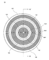
図1は、本発明の一実施形態に係るヒータユニットの全体構成を示す上面図である。図2は、図1のA−A’断面図である。図1及び図2に示すように、第1実施形態に係るヒータユニット10は、カバー部110、基材120、蓋部130、ヒータ部140、及び絶縁層150を有する。ヒータ部140は、それぞれ独立して制御される第1ヒータ部142、第2ヒータ部144、及び第3ヒータ部146を含む。ここで、第1ヒータ部142、第2ヒータ部144、及び第3ヒータ部146を特に区別しないときはヒータ部140という。基材120には第1ヒータ部142と第2ヒータ部144との間に設けられた第1の溝123、及び第2ヒータ部144と第3ヒータ部146との間に設けられた第2の溝125が設けられている。第1ヒータ部142、第2ヒータ部144、及び第3ヒータ部146は、それぞれ外部接続端子1421、1441、及び1461を介して、異なるヒータコントローラに接続されている。
[Configuration of Heater Unit 10]
FIG. 1 is a top view showing an overall configuration of a heater unit according to an embodiment of the present invention. 2 is a cross-sectional view taken along line AA ′ of FIG. As shown in FIGS. 1 and 2, the
図2に示すように、ヒータユニット10はチャンバ15によって囲まれている。チャンバ15はカバー部110に接続されており、チャンバ内の空間とチャンバ外の大気とを隔離している。カバー部110は一部がチャンバ15内部に配置され、一部がチャンバ15外部に配置されている。カバー部110は中空構造を有しており、カバー部110の内部は大気に露出しており、カバー部110の外部はチャンバ内の空間に露出している。チャンバ15とカバー部110とは、溶接等により固定されていてもよく、金属製ガスケットや樹脂製Oリングなどを介して脱着可能に接続されていてもよい。
As shown in FIG. 2, the
基材120はカバー部110上に配置されている。上記のように基材120には、第1ヒータ部142と第2ヒータ部144との間に対応する領域に第1の溝123が設けられ、第2ヒータ部144と第3ヒータ部146との間に対応する領域に第2の溝125が設けられている。第1の溝123及び第2の溝125は、基材120の上面側に開口端を有し、基材120の下面側に底部を有する凹部である。第1の溝123及び第2の溝125の基材120に対する深さは基板120の表面から5mm以上(基板120の板厚マイナス5mm以下)である。ここで、第1の溝123は基材120の第1ゾーン122と第2ゾーン124との間に設けられており、第2の溝125は第2ゾーン124と第3ゾーン126との間に設けられている、ということもできる。
The
蓋部130は基材120上に配置されている。つまり、蓋部130は第1の溝123及び第2の溝125の開口端側に配置されている。蓋部130は平板形状を有しており、少なくとも第1の溝123及び第2の溝125の各々の開口端を塞ぐように配置されている。つまり、蓋部130は第1の溝123又は第2の溝125と共に閉空間を構成する。蓋部130は、例えばインジウム(In)、スズ(Sn)、及びこれらを含む合金などのろう材を介して基材120にろう付けされている。これらのろう材は基材120の上面において、第1の溝123及び第2の溝125を除く領域に配置されている。ここで、ろう材が第1の溝123及び第2の溝125の内部に入り込まないように、第1の溝123及び第2の溝125に対して十分なオフセットを設けられて基材120の上面に配置されてもよい。
The
絶縁層150は蓋部130の上方に配置されており、ヒータ部140は蓋部130と絶縁層150との間に配置されている。つまり、ヒータ部140は蓋部130及び絶縁層150によって覆われている。換言すると、ヒータ部140は、上面が平坦な蓋部130と下面に凹部が設けられた絶縁層150とによって覆われている、ということもできる。
The insulating
ここで、第1の溝123内部及び第2の溝125内部は真空又は減圧雰囲気である。各々の溝の内部が真空又は減圧雰囲気であることで、基材120の第1ゾーン122と第2ゾーン124との間、第2ゾーン124と第3ゾーン126との間で熱交換されにくくなり、これらのゾーンを効率よく断熱することができる。第1の溝123内部及び第2の溝125内部を真空又は減圧雰囲気にするためには、上記のろう付け工程において、真空又は減圧雰囲気の環境下で基材120上に蓋部130を配置すればよい。
Here, the inside of the
上記では、第1の溝123内部及び第2の溝125内部が真空又は減圧雰囲気である構成を例示したが、この構成に限定されない。例えば、第1の溝123内部及び第2の溝125内部にガスが充填されていてもよい。又は、第1の溝123内部及び第2の溝125内部に基材120より熱伝導率が低い物質(充填材)が充填されていてもよい。充填される物質は樹脂材料などの固体であってもよく、オイルなどの液体であってもよい。これらの構成であっても、第1の溝123及び第2の溝125はチャンバ15内の空間温度による影響を受けにくくすることができるため、使用環境に依存しない安定した断熱効果を得ることができる。
In the above description, the configuration in which the inside of the
[ヒータユニット10の各構成部品の材料]
カバー部110としては、アルミニウム(Al)、チタン(Ti)、ステンレス(SUS)などの材料を用いることができる。基材120としては、金属基材又は半導体基材を用いることができる。金属基材としては、Al基材、Ti基材、SUS基材などを用いることができる。半導体基材としては、シリコン(Si)基材、シリコンカーバイト(SiC)基材、ガリウムナイトライド(GaN)基材などを用いることができる。基材120の熱伝導率は、好ましくは100W/mK以上であるとよい。本実施形態では、基材120としてAlを用いている。
[Material of each component of heater unit 10]
As the
蓋部130としては、Ti、SUS、酸化シリコン(SiO2)、酸化アルミニウム(Al2O3)などを用いることができる。蓋部130は基材120よりも熱伝導率が低い材料を用いることができ、基材120に用いられる材料の熱伝導率に応じて適宜選択することができる。また、蓋部130は絶縁層150よりも熱伝導率が低い材料を用いることができ、絶縁層150に用いられる材料の熱伝導率に応じて適宜選択することができる。本実施形態では、蓋部130としてSUSを用いている。
As the
蓋部130としてSUSを用いた場合、異なるゾーン間の熱交換による影響を小さくするため、SUSの厚さは1mm以下とするとよい。ここで、熱伝導率が低い蓋部130を実現するために、蓋部130が気孔を有する材料であってもよい。換言すると、蓋部130は多孔質(ポーラス)な材料であってもよい。蓋部130としてポーラスな材料を用いる場合、気孔の含有率が1%以上20%以下の蓋部130を用いることができる。好ましくは蓋部130の気孔の含有率は10%以上20%以下であるとよい。なお、蓋部130としてポーラスな材料を用いる場合、ガスを透過しない材料を用いることが好ましい。ただし、第1の溝123内部及び第2の溝125内部における真空又は減圧雰囲気を維持できる範囲であれば、ガスを透過するポーラスな材料を用いてもよい。また、上記溝の内部にガスや充填材が充填されている場合についても、当該充填材を維持できる範囲であれば、ガスを透過するポーラスな材料を用いてもよい。ここで、例えば蓋部130としてポーラスなSUSを用いた場合、ポーラスなSUSの熱伝導率はSUSのバルクの熱伝導率(約16.7W/mK)よりも小さくなる。具体的には、ポーラスなSUSの熱伝導率は2W/mK以上16W/mK以下である。なお、上記の熱伝導率はレーザフラッシュ法によって測定された25℃のときの値である。
When SUS is used as the
ポーラスなSUSは、例えばコールドスプレー法で形成することができる。ここでは、板状の蓋部130を基材120にろう付けするため、基材120とは異なる部材上にポーラスな板状のSUSを形成した後に基材120にろう付けする。コールドスプレー法とは、材料を溶融またはガス化させることなく、不活性ガスと共に超音速流で固相状態のまま基材に衝突させて皮膜を形成する方法である。例えば、SUSの厚さを調節するために、SUSをコールドスプレー法で形成した後に研削することで所望の厚さまで薄膜化することで蓋部130を得ることができる。SUSをコールドスプレー法で形成することで、上記に示すようなポーラスなSUSの層を実現することができる。コールドスプレー法の形成条件を調整することで、ポーラスなSUSの層に対する気孔の含有率を調整することができる。また、SUSはコールドスプレー法以外の方法で形成してもよい。
Porous SUS can be formed by, for example, a cold spray method. Here, in order to braze the plate-shaped
上記では、ポーラスなSUSを形成するためにコールドスプレー法を用いてSUSを形成したが、コールドスプレー法以外にも、プラズマ溶射、フレーム溶射、アーク溶射、高速フレーム溶射(HVOF:High Velocity Oxygen Fuel、又はHVAF:High Velocity Air Fuel)、ウォームスプレー等の方法で形成することができる。一方、気孔を有さない又は気孔の含有率が1%以下のSUSを形成する場合はスパッタリング法、ろう付け、及び拡散接合等の方法を用いることができる。 In the above, SUS was formed using a cold spray method in order to form a porous SUS. However, in addition to the cold spray method, plasma spraying, flame spraying, arc spraying, high-speed flame spraying (HVOF: High Velocity Oxygen Fuel, Alternatively, it can be formed by a method such as HVAF: High Velocity Air Fuel) or warm spray. On the other hand, when forming SUS having no pores or having a pore content of 1% or less, methods such as sputtering, brazing, and diffusion bonding can be used.
ヒータ部140は、電流によってジュール熱を発生する導電体を用いることができる。ヒータ部140としては、タングステン(W)、タンタル(Ta)、モリブデン(Mo)、白金(Pt)などの高融点金属を用いることができる。ただし、ヒータ部140は上記の高融点金属以外にも、鉄(Fe)、クロム(Cr)、及びAlを含む合金や、ニッケル(Ni)及びCrを含む合金や、SiC、モリブデンシリサイド、及びカーボン(C)などの非金属体を用いることができる。本実施形態では、ヒータ部140としてWを用いている。
The
絶縁層150は、ヒータ部140が他の部材と電気的に接続されることを抑制するために配置される。つまり、ヒータ部140を他の部材から十分に絶縁性させる材料を用いることができる。絶縁層150としては、Al2O3、窒化アルミニウム(AlN)、SiO2、窒化シリコン(SiN)などを用いることができる。本実施形態では、絶縁層150としてAl2O3を用いている。
The insulating
図2に示すヒータユニット10のように、第1の溝123の開口端及び第2の溝125の開口端が蓋部130で塞がれていることで、製造工程において意図しない部材が第1の溝123及び第2の溝125の内部に入り込むことを防ぐことができる。例えば、基材120上にヒータ部140及び絶縁層150を形成する場合、ヒータ部140の材料の一部や絶縁層150の材料の一部が第1の溝123及び第2の溝125の内部に入り込むことを防ぐことができる。また、ヒータ部140及び絶縁層150を基材120に接着する接着剤の一部が第1の溝123及び第2の溝125の内部に形成されることを防ぐことができる。意図しない部材が第1の溝123及び第2の溝125の内部に形成されてしまうと、基材に設けられた溝によるゾーン間の断熱効率が悪化してしまうが、ヒータユニット10の構造によると、ゾーン間の断熱効率の悪化を抑制することができる。また、第1の溝123及び第2の溝125には、基材120の面内において均一に真空が保たれる、又は、ガス、充填材が充填されているため、ゾーン間の断熱性能の面内ばらつきを低減することができる。
Like the
図2では、蓋部130及び絶縁層150によってヒータ部140が挟持された構造を例示したが、この構造に限定されない。例えば、絶縁層150の内部にヒータ部140が埋め込まれていてもよい。
In FIG. 2, the structure in which the
また、図2では、基材120と蓋部130とが接している構造を例示したが、基材120と蓋部130との間に他の層が配置されていてもよい。この場合、他の層にはパターンが形成されていてもよく、パターンが形成されていなくてもよい。同様に、図2では、蓋部130と絶縁層150とが接している構造を例示したが、蓋部130と絶縁層150との間に他の層が配置されていてもよい。
2 illustrates the structure in which the
以上のように、第1実施形態のヒータユニット10によると、第1の溝123及び蓋部130によって閉空間が構成されていることで、第1ゾーン122と第2ゾーン124との間の高い断熱効果を得ることができる。同様に、第2の溝125及び蓋部130によって閉空間が構成されることで、第2ゾーン124と第3ゾーン126との間の高い断熱効果を得ることができる。上記の閉空間が構成された溝による断熱効果は使用環境に依存せず、各ゾーンの温度の制御性を高めることができるため、温度の面内均一性が高く、ヒータを設置したゾーン毎に意図的に温度差をつけることが可能なヒータユニットを提供することができる。上記のように、第1実施形態のヒータユニット10はゾーン毎に意図的に温度差をつけることが可能であるため、使用環境に応じて各ゾーンの温度を正確にコントロールすることができる。
As described above, according to the
また、当該閉空間が真空であることで、異なるゾーン間のより高い断熱効果を得ることができる。また、当該閉空間がガスや充填材によって充填されている構成によっても、異なるゾーン間のより高い断熱効果を得ることができる。 Moreover, the higher heat insulation effect between different zones can be acquired because the said closed space is a vacuum. Moreover, the higher heat insulation effect between different zones can be acquired also by the structure with which the said closed space is filled with gas or a filler.
なお、第1実施形態では、第1ヒータ部142、第2ヒータ部144、及び第3ヒータ部146の3つのヒータ部にそれぞれ対応する第1ゾーン122、第2ゾーン124、及び第3ゾーン126を分離するために、第1の溝123及び第2の溝125の2つの溝が基材120に設けられた構成を例示したが、この構成に限定されない。基材120に設けられる溝の数は、分離すべきゾーンの数に応じて適宜設定すればよい。また、第1の溝123及び第2の溝125が平面視において円形の構成を例示したが、この構成に限定されない。第1の溝123及び第2の溝125の形状は各ヒータ部の形状に応じて設計することができる。例えば、第1の溝123及び第2の溝125の形状は矩形であってもよく、矩形以外の多角形であってもよい。また、第2ゾーン124が第1ゾーン122を囲み、第3ゾーン126が第1ゾーン122及び第2ゾーン124を囲む構成を例示したが、この構成に限定されない。複数のゾーンは上記以外の多様な形状に分割されていてもよい。例えば、複数のゾーンは基材120の中心を基準に上下左右に基材120を4分割されたゾーンであってもよい。
In the first embodiment, the
〈第2実施形態〉
図3を用いて、本発明の第2実施形態に係るヒータユニットの断面構造について説明する。本発明の第2実施形態に係るヒータユニットは、第1実施形態と同様に複数のゾーンに分割して独立して制御されるヒータ部を有する。また、第2実施形態に係るヒータユニットは、CVD装置、スパッタ装置、蒸着装置、エッチング装置、プラズマ処理装置、測定装置、検査装置、及び顕微鏡等に使用することができる。ただし、第2実施形態に係るヒータユニットは上記の装置に使用するものに限定されず、基板を加熱する必要がある装置に対して使用することができる。
Second Embodiment
The cross-sectional structure of the heater unit according to the second embodiment of the present invention will be described with reference to FIG. The heater unit according to the second embodiment of the present invention has a heater unit that is divided into a plurality of zones and controlled independently, as in the first embodiment. The heater unit according to the second embodiment can be used for a CVD apparatus, a sputtering apparatus, a vapor deposition apparatus, an etching apparatus, a plasma processing apparatus, a measurement apparatus, an inspection apparatus, a microscope, and the like. However, the heater unit according to the second embodiment is not limited to the one used in the above apparatus, and can be used for an apparatus that needs to heat the substrate.
[ヒータユニット20の構成]
第2実施形態のヒータユニット20の上面図は第1実施形態のヒータユニット10と同様であるので、ここでは説明を省略する。また、ヒータユニット20の断面図はヒータユニット10の断面図と類似しているため、ヒータユニット20の説明において、ヒータユニット10と同様の構造に関しては説明を省略し、主に相違点について説明する。なお、ヒータユニット20の蓋部130は、例えばIn、Sn、及びこれらを含む合金などのろう材を介して基材120にろう付けされている。
[Configuration of Heater Unit 20]
Since the top view of the
図3は、本発明の一実施形態に係るヒータユニットの断面図である。図3に示すように、ヒータユニット20の絶縁層150には、第1の溝123に対応する領域に第3の溝153が設けられ、第2の溝125に対応する領域に第4の溝155が設けられている点において、ヒータユニット10とは相違する。つまり、ヒータユニット20では、第1ヒータ部142を覆う絶縁層150と第2ヒータ部144を覆う絶縁層150との間に第3の溝153が設けられており、第2ヒータ部144を覆う絶縁層150と第3ヒータ部146を覆う絶縁層150との間に第4の溝155が設けられている。
FIG. 3 is a cross-sectional view of a heater unit according to an embodiment of the present invention. As shown in FIG. 3, the insulating
図3では、第3の溝153及び第4の溝155は、絶縁層150の厚さ方向に絶縁層150が全て除去されており、第3の溝153及び第4の溝155によって蓋部130が露出されている。また、第3の溝153は第1の溝123と同じ領域に設けられており、第4の溝155は第2の溝125と同じ領域に設けられている。つまり、平面視において、第1の溝123と第3の溝153とは重畳しており、第2の溝125と第4の溝155とは重畳している。
In FIG. 3, the
以上のように、第2実施形態のヒータユニット20によると、絶縁層150に第3の溝153が設けられていることで、第1ヒータ部142で発生した熱が第2ヒータ部144の領域に伝わりにくくなる。つまり、第1ヒータ部142と第2ヒータ部144との干渉を抑制することができる。同様に、絶縁層150に第4の溝155が設けられていることで、第2ヒータ部144と第3ヒータ部146との干渉を抑制することができる。その結果、各ゾーンの温度制御性を高めることができるため、温度の面内均一性が高いヒータユニットを提供することができる。
As described above, according to the
なお、第2実施形態では、第3の溝153及び第4の溝155が、絶縁層150の厚さ方向に絶縁層150が全て除去された構造を例示したが、この構造に限定されない。例えば、第3の溝153及び第4の溝155の両方又はいずれか一方が、絶縁層150の厚さ方向に絶縁層150が一部だけ除去されていてもよい。つまり、第3の溝153及び第4の溝155の両方又はいずれか一方が、絶縁層150に設けられた有底孔であってもよい。
In the second embodiment, the
また、第2実施形態では、第3の溝153は第1の溝123と同じ領域に設けられ、第4の溝155は第2の溝125と同じ領域に設けられた構造を例示したが、この構造に限定されない。第3の溝153は少なくとも第1ヒータ部142と第2ヒータ部144との間に設けられ、第4の溝155は少なくとも第2ヒータ部144と第3ヒータ部146との間に設けられていればよく、必ずしも第1の溝123及び第2の溝125と同じ領域に設けられていなくてもよい。
In the second embodiment, the
〈第3実施形態〉
図4を用いて、本発明の第3実施形態に係るヒータユニットの断面構造について説明する。本発明の第3実施形態に係るヒータユニットは、第1実施形態と同様に複数のゾーンに分割して独立して制御されるヒータ部を有する。また、第3実施形態に係るヒータユニットは、CVD装置、スパッタ装置、蒸着装置、エッチング装置、プラズマ処理装置、測定装置、検査装置、及び顕微鏡等に使用することができる。ただし、第3実施形態に係るヒータユニットは上記の装置に使用するものに限定されず、基板を加熱する必要がある装置に対して使用することができる。
<Third Embodiment>
The cross-sectional structure of the heater unit according to the third embodiment of the present invention will be described with reference to FIG. The heater unit according to the third embodiment of the present invention has a heater unit that is divided into a plurality of zones and controlled independently as in the first embodiment. The heater unit according to the third embodiment can be used for a CVD apparatus, a sputtering apparatus, a vapor deposition apparatus, an etching apparatus, a plasma processing apparatus, a measurement apparatus, an inspection apparatus, a microscope, and the like. However, the heater unit according to the third embodiment is not limited to that used in the above apparatus, and can be used for an apparatus that needs to heat the substrate.
[ヒータユニット30の構成]
第3実施形態のヒータユニット30の上面図は第1実施形態のヒータユニット10と同様であるので、ここでは説明を省略する。また、ヒータユニット30の断面図はヒータユニット10の断面図と類似しているため、ヒータユニット30の説明において、ヒータユニット10と同様の構造に関しては説明を省略し、主に相違点について説明する。なお、ヒータユニット30の蓋部130は、例えばIn、Sn、及びこれらを含む合金などのろう材を介して基材120にろう付けされている。
[Configuration of Heater Unit 30]
Since the top view of the
図4は、本発明の一実施形態に係るヒータユニットの断面図である。図4に示すように、ヒータユニット30では、ヒータ部140が基材120に埋め込まれている点において、ヒータユニット10とは相違する。具体的には、ヒータユニット30では、第1ヒータ部142が基材120の第1ゾーン122に埋め込まれており、第2ヒータ部144が第2ゾーン124に埋め込まれており、第3ヒータ部146が第3ゾーン126に埋め込まれている。
FIG. 4 is a cross-sectional view of a heater unit according to an embodiment of the present invention. As shown in FIG. 4, the
図4では、第1ヒータ部142、第2ヒータ部144、及び第3ヒータ部146がそれぞれ基材120に埋め込まれた構造を例示したが、この構造に限定されない。例えば、第1ヒータ部142、第2ヒータ部144、及び第3ヒータ部146の各々の表面が基材120から露出しており、各ヒータ部が蓋部130と接触していてもよい。
In FIG. 4, the structure in which the
以上のように、第3実施形態のヒータユニット30によると、第1ヒータ部142、第2ヒータ部144、及び第3ヒータ部146の各々が基材120に埋め込まれており、各ヒータ部の間に閉空間を構成する溝が設けられていることで、異なるゾーン間の高い断熱効果を得ることができる。上記の閉空間が構成された溝による断熱効果は使用環境に依存せず、各ゾーンの温度制御性を高めることができるため、温度の面内均一性が高く、ヒータを設置したゾーン毎に意図的に温度差をつけることが可能なヒータユニットを提供することができる。
As described above, according to the
〈第4実施形態〉
図5を用いて、本発明の第4実施形態に係るヒータユニットの断面構造について説明する。本発明の第4実施形態に係るヒータユニットは、第1実施形態と同様に複数のゾーンに分割して独立して制御されるヒータ部を有する。また、第4実施形態に係るヒータユニットは、CVD装置、スパッタ装置、蒸着装置、エッチング装置、プラズマ処理装置、測定装置、検査装置、及び顕微鏡等に使用することができる。ただし、第4実施形態に係るヒータユニットは上記の装置に使用するものに限定されず、基板を加熱する必要がある装置に対して使用することができる。
<Fourth embodiment>
The cross-sectional structure of the heater unit according to the fourth embodiment of the present invention will be described with reference to FIG. The heater unit according to the fourth embodiment of the present invention has a heater unit that is divided into a plurality of zones and controlled independently, as in the first embodiment. The heater unit according to the fourth embodiment can be used for a CVD apparatus, a sputtering apparatus, a vapor deposition apparatus, an etching apparatus, a plasma processing apparatus, a measurement apparatus, an inspection apparatus, a microscope, and the like. However, the heater unit according to the fourth embodiment is not limited to that used in the above apparatus, and can be used for an apparatus that needs to heat the substrate.
[ヒータユニット40の構成]
第4実施形態のヒータユニット40の上面図は第1実施形態のヒータユニット10と同様であるので、ここでは説明を省略する。また、ヒータユニット40の断面図はヒータユニット10の断面図と類似しているため、ヒータユニット40の説明において、ヒータユニット10と同様の構造に関しては説明を省略し、主に相違点について説明する。なお、ヒータユニット40の蓋部130は、例えばIn、Sn、及びこれらを含む合金などのろう材を介して基材120にろう付けされている。
[Configuration of Heater Unit 40]
Since the top view of the
図5は、本発明の一実施形態に係るヒータユニットの断面図である。図5に示すように、ヒータユニット40は、絶縁層150上に静電チャック部160(ESC;ElectroStatic Chuck)をさらに有する点において、ヒータユニット10とは相違する。ここで、静電チャック部160は絶縁層150を介して基材120に取り付けられている、ということもできる。静電チャック部160は接着剤を介して絶縁層150に接着されている。静電チャックとは、ステージの上に誘電層を設け、ステージと処理基板との間に電圧を印加し、両者の間に発生した力によって処理基板を吸着する機構である。静電チャックは、機械的な保持具を使用しないために処理基板全面を均一に成膜又は加工することができる。
FIG. 5 is a cross-sectional view of a heater unit according to an embodiment of the present invention. As shown in FIG. 5, the
以上のように、第4実施形態のヒータユニット40によると、第1実施形態と同様の効果を得ることができ、さらに、処理基板の全面を均一に成膜又は加工することができる。また、例えばメカクランプなどの基板保持機構を用いて処理基板を保持する場合、メカクランプと処理基板との接触箇所を介して処理基板の熱がメカクランプに伝達され、接触箇所付近の処理基板の温度が低下し、基板温度の面内均一性が低下してしまうが、静電チャックを用いて処理基板を保持することで、上記の基板温度の面内均一性の低下を抑制することができる。
As described above, according to the
〈第5実施形態〉
図6を用いて、本発明の第5実施形態に係るヒータユニットの断面構造について説明する。本発明の第5実施形態に係るヒータユニットは、第1実施形態と同様に複数のゾーンに分割して独立して制御されるヒータ部を有する。また、第5実施形態に係るヒータユニットは、CVD装置、スパッタ装置、蒸着装置、エッチング装置、プラズマ処理装置、測定装置、検査装置、及び顕微鏡等に使用することができる。ただし、第5実施形態に係るヒータユニットは上記の装置に使用するものに限定されず、基板を加熱する必要がある装置に対して使用することができる。
<Fifth Embodiment>
The cross-sectional structure of the heater unit according to the fifth embodiment of the present invention will be described with reference to FIG. The heater unit according to the fifth embodiment of the present invention has a heater unit that is divided into a plurality of zones and controlled independently as in the first embodiment. The heater unit according to the fifth embodiment can be used for a CVD apparatus, a sputtering apparatus, a vapor deposition apparatus, an etching apparatus, a plasma processing apparatus, a measurement apparatus, an inspection apparatus, a microscope, and the like. However, the heater unit according to the fifth embodiment is not limited to the one used in the above apparatus, and can be used for an apparatus that needs to heat the substrate.
[ヒータユニット50の構成]
第5実施形態のヒータユニット50の上面図は第1実施形態のヒータユニット10と同様であるので、ここでは説明を省略する。また、ヒータユニット50の断面図は図3に示すヒータユニット20の断面図と類似しているため、ヒータユニット50の説明において、ヒータユニット20と同様の構造に関しては説明を省略し、主に相違点について説明する。なお、ヒータユニット50の蓋部130は、例えばIn、Sn、及びこれらを含む合金などのろう材を介して基材120にろう付けされている。
[Configuration of heater unit 50]
Since the top view of the
図6は、本発明の一実施形態に係るヒータユニットの断面図である。図6に示すように、ヒータユニット50は、第3の溝153及び第4の溝155が設けられた絶縁層150上に静電チャック部160をさらに有する点において、ヒータユニット20とは相違する。静電チャック部160は接着剤を介して絶縁層150に接着されている。ヒータユニット20では、第3の溝153及び第4の溝155はそれぞれ開口端が閉じておらず、それぞれの溝の内部の空間とチャンバ15の空間とがつながっていたが、ヒータユニット50では、第3の溝153及び第4の溝155は静電チャック部160と共に閉空間を構成している。
FIG. 6 is a cross-sectional view of a heater unit according to an embodiment of the present invention. As shown in FIG. 6, the
ここで、第3の溝153内部及び第4の溝155内部は真空又は減圧雰囲気である。各々の溝の内部が真空又は減圧雰囲気であることで、第1ヒータ部142、第2ヒータ部144、及び第3ヒータ部146の間の干渉を抑制することができる。また、第3の溝153内部及び第4の溝155内部にガスが充填されていてもよく、基材120より熱伝導率が低い物質(充填材)が充填されていてもよい。
Here, the inside of the
以上のように、第5実施形態のヒータユニット50によると、第3の溝153及び静電チャック部160によって閉空間が構成されていることで、第1ヒータ部142と第2ヒータ部144との間の干渉を抑制することができる。同様に、第4の溝155及び静電チャック部160によって閉空間が構成されていることで、第2ヒータ部144と第3ヒータ部146との間の干渉を抑制することができる。その結果、各ゾーンの温度制御性を高めることができるため、温度の面内均一性が高く、ヒータを設置したゾーン毎に意図的に温度差をつけることが可能なヒータユニットを提供することができる。また、静電チャックを用いて処理基板を保持することで、上記の基板温度の面内均一性の低下を抑制することができる。
As described above, according to the
〈第6実施形態〉
図7を用いて、本発明の第6実施形態に係るヒータユニットの断面構造について説明する。本発明の第6実施形態に係るヒータユニットは、第1実施形態と同様に複数のゾーンに分割して独立して制御されるヒータ部を有する。また、第6実施形態に係るヒータユニットは、CVD装置、スパッタ装置、蒸着装置、エッチング装置、プラズマ処理装置、測定装置、検査装置、及び顕微鏡等に使用することができる。ただし、第6実施形態に係るヒータユニットは上記の装置に使用するものに限定されず、基板を加熱する必要がある装置に対して使用することができる。
<Sixth Embodiment>
The cross-sectional structure of the heater unit according to the sixth embodiment of the present invention will be described with reference to FIG. The heater unit according to the sixth embodiment of the present invention has a heater unit that is divided into a plurality of zones and controlled independently as in the first embodiment. The heater unit according to the sixth embodiment can be used for a CVD apparatus, a sputtering apparatus, a vapor deposition apparatus, an etching apparatus, a plasma processing apparatus, a measurement apparatus, an inspection apparatus, a microscope, and the like. However, the heater unit according to the sixth embodiment is not limited to that used in the above apparatus, and can be used for an apparatus that needs to heat the substrate.
[ヒータユニット60の構成]
第6実施形態のヒータユニット60の上面図は第1実施形態のヒータユニット10と同様であるので、ここでは説明を省略する。また、ヒータユニット60の断面図は、図4に示すヒータユニット30の断面図と類似しているため、ヒータユニット60の説明において、ヒータユニット30と同様の構造に関しては説明を省略し、主に相違点について説明する。なお、ヒータユニット60の蓋部130は、例えばIn、Sn、及びこれらを含む合金などのろう材を介して基材120にろう付けされている。
[Configuration of Heater Unit 60]
Since the top view of the
図7は、本発明の一実施形態に係るヒータユニットの断面図である。図7に示すように、ヒータユニット60は、蓋部130上に静電チャック部160をさらに有する点において、ヒータユニット30とは相違する。静電チャック部160は接着剤を介して蓋部130に接着されている。
FIG. 7 is a cross-sectional view of a heater unit according to an embodiment of the present invention. As shown in FIG. 7, the
ここで、静電チャック部160を第1の溝123及び第2の溝125が設けられた基材120に直接取り付ける場合、接着剤を用いて基材120と静電チャック部160とを接着する必要がある。基材120と静電チャック部160とを直接接着すると、接着剤の一部が第1の溝123及び第2の溝125の内部に入り込んでしまう。接着剤が第1の溝123及び第2の溝125の内部に形成されてしまうと、ゾーン間の断熱効率が悪化してしまうという問題がある。
Here, when directly attaching the
ヒータユニット60の構造によると、静電チャック部160は、第1の溝123及び第2の溝125の開口端を塞ぐ蓋部130の上面に接着されるため、基板に設けられた溝の内部に接着剤が入り込むことを防ぐことができる。これによって、ゾーン間の断熱効率の悪化を抑制することができ、温度の面内均一性が高く、ヒータを設置したゾーン毎に意図的に温度差をつけることが可能なヒータユニットを提供することができる。
According to the structure of the
〈第7実施形態〉
図8及び図9を用いて、本発明の第7実施形態に係るヒータユニットの断面構造について説明する。本発明の第7実施形態に係るヒータユニットは、第1実施形態と同様に複数のゾーンに分割して独立して制御されるヒータ部を有する。また、第7実施形態に係るヒータユニットは、CVD装置、スパッタ装置、蒸着装置、エッチング装置、プラズマ処理装置、測定装置、検査装置、及び顕微鏡等に使用することができる。ただし、第7実施形態に係るヒータユニットは上記の装置に使用するものに限定されず、基板を加熱する必要がある装置に対して使用することができる。
<Seventh embodiment>
The cross-sectional structure of the heater unit according to the seventh embodiment of the present invention will be described with reference to FIGS. The heater unit according to the seventh embodiment of the present invention has a heater unit that is divided into a plurality of zones and controlled independently, as in the first embodiment. The heater unit according to the seventh embodiment can be used for a CVD apparatus, a sputtering apparatus, a vapor deposition apparatus, an etching apparatus, a plasma processing apparatus, a measurement apparatus, an inspection apparatus, a microscope, and the like. However, the heater unit according to the seventh embodiment is not limited to that used in the above apparatus, and can be used for an apparatus that needs to heat the substrate.
[ヒータユニット70の構成]
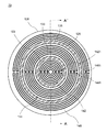
図8は、本発明の一実施形態に係るヒータユニットの全体構成を示す上面図である。図9は、図8のA−A’断面図である。また、ヒータユニット70はヒータユニット10と類似しているため、ヒータユニット70の説明において、ヒータユニット10と同様の構造に関しては説明を省略し、主に相違点について説明する。
[Configuration of Heater Unit 70]
FIG. 8 is a top view showing the overall configuration of the heater unit according to one embodiment of the present invention. 9 is a cross-sectional view taken along the line AA ′ of FIG. In addition, since the
図8に示すように、ヒータユニット70は第1ヒータ部142と第2ヒータ部144との間に配置された第1蓋部133と、第2ヒータ部144と第3ヒータ部146との間に配置された第2蓋部135と、を有する。つまり、ヒータユニット70において、第1の溝123、第2の溝125は基材120の平面視においてリング状に設けられている。また、第1蓋部133及び第2蓋部135はリング形状である。第1蓋部133は、平面視において第1の溝123と重畳するように配置されている。また、第2蓋部135は平面視において第2の溝125と重畳するように配置されている。第7実施形態は、第1実施形態の蓋部130を第1蓋部133及び第2蓋部135に置き換え、第1の溝123及び第2の溝125の断面形状を変更した実施形態である。
As shown in FIG. 8, the
図9に示すように、第1の溝123及び第2の溝125は共に基材120の表面付近の開口幅が他の箇所よりも大きくなっており、開口幅が大きくなった領域に第1蓋部133及び第2蓋部135が配置されている。ここで、第1の溝123及び第2の溝125の基材120の表面付近の開口幅は第1蓋部133及び第2蓋部135の幅よりも大きい。また、第1蓋部133及び第2蓋部135の上面と基材120の上面とは略同一平面である。第1蓋部133及び第2蓋部135は、例えばIn、Sn、及びこれらを含む合金などのろう材を介して基材120にろう付けされている。ここでは、第1蓋部133及び第2蓋部135の下面側が基材120にろう付けされている。第1蓋部133及び第2蓋部135としては、蓋部130と同様の材料を用いることができる。
As shown in FIG. 9, both the
なお、第1蓋部133の上面及び第2蓋部135の上面は基材120の上面よりも上方に突出していてもよく、逆に基材120の上面よりも基材120の内部側(基材120の上面よりも下方)に位置していてもよい。また、第1蓋部133及び第2蓋部135は、各々の蓋部の側面又は各々の蓋部の下面及び側面の両方で基材120にろう付けされていてもよい。また、第4実施形態に示すように、絶縁層150上に静電チャック部が配置されていてもよい。
Note that the upper surface of the
以上のように、第7実施形態のヒータユニット70によると、第1の溝123及び第2の溝125の開口端部を塞ぐ蓋部の材料費を低減することができるだけでなく、基材120に対する第1蓋部133及び第2蓋部135のアライメントを容易にし、ヒータユニット70の高さを低減することができる。
As described above, according to the
なお、本発明は上記の実施形態に限られたものではなく、趣旨を逸脱しない範囲で適宜変更することが可能である。 Note that the present invention is not limited to the above-described embodiment, and can be modified as appropriate without departing from the spirit of the present invention.
10、20、30、40、50、60、70:ヒータユニット、 15:チャンバ、 110:カバー部、 120:基材、 122:第1ゾーン、 123:第1の溝、 124:第2ゾーン、 125:第2の溝、 126:第3ゾーン、 130:蓋部、 133:第1蓋部、 135:第2蓋部、 140:ヒータ部、 142:第1ヒータ部、 144:第2ヒータ部、 146:第3ヒータ部、 150:絶縁層、 153:第3の溝、 155:第4の溝、 160:静電チャック部、 1421、1441、1461:外部接続端子 10, 20, 30, 40, 50, 60, 70: heater unit, 15: chamber, 110: cover part, 120: base material, 122: first zone, 123: first groove, 124: second zone, 125: second groove, 126: third zone, 130: lid part, 133: first lid part, 135: second lid part, 140: heater part, 142: first heater part, 144: second heater part 146: third heater section, 150: insulating layer, 153: third groove, 155: fourth groove, 160: electrostatic chuck section, 1421, 1441, 1461: external connection terminals
Claims (7)
前記第1ヒータ部とは独立して制御される第2ヒータ部と、
前記第1ヒータ部と前記第2ヒータ部との間に対応する領域に溝が設けられた基材と、
前記溝の開口端に配置され、前記溝と共に閉空間を提供する蓋部と、
を有し、
前記蓋部は、前記第1ヒータ部と前記基材との間、及び前記第2ヒータ部と前記基材との間に設けられていることを特徴とするヒータユニット。 A first heater section;
A second heater part controlled independently of the first heater part;
A base material provided with a groove in a corresponding region between the first heater part and the second heater part;
A lid that is disposed at the open end of the groove and provides a closed space with the groove;
I have a,
The said cover part is provided between the said 1st heater part and the said base material, and between the said 2nd heater part and the said base material, The heater unit characterized by the above-mentioned .
前記絶縁層を介して前記基材に取り付けられた静電チャックと、
をさらに有することを特徴とする請求項1に記載のヒータユニット。 An insulating layer covering the first heater part and the second heater part;
An electrostatic chuck attached to the substrate via the insulating layer;
The heater unit according to claim 1, further comprising:
前記第1ヒータ部とは独立して制御される第2ヒータ部と、
前記第1ヒータ部と前記第2ヒータ部との間に対応する領域に溝が設けられた基材と、
前記溝の開口端に配置され、前記溝と共に閉空間を提供する蓋部と、
を有し、
前記溝は、前記基材の平面視においてリング状に設けられ、
前記蓋部は、リング形状であることを特徴とするヒータユニット。
A first heater section;
A second heater part controlled independently of the first heater part;
A base material provided with a groove in a corresponding region between the first heater part and the second heater part;
A lid that is disposed at the open end of the groove and provides a closed space with the groove;
Have
The groove is provided in a ring shape in a plan view of the base material,
The lid, features and to Ruhi Tayunitto that it is ring-shaped.
Priority Applications (7)
| Application Number | Priority Date | Filing Date | Title |
|---|---|---|---|
| JP2015209886A JP6584286B2 (en) | 2015-10-26 | 2015-10-26 | Heater unit |
| CN201680059985.2A CN108141917B (en) | 2015-10-26 | 2016-09-28 | Heater unit |
| PCT/JP2016/078575 WO2017073230A1 (en) | 2015-10-26 | 2016-09-28 | Heater unit |
| EP16859467.9A EP3370477B1 (en) | 2015-10-26 | 2016-09-28 | Heater unit |
| KR1020187008003A KR102093048B1 (en) | 2015-10-26 | 2016-09-28 | Heater unit |
| TW105133771A TWI629727B (en) | 2015-10-26 | 2016-10-19 | Heater unit |
| US15/948,473 US10290529B2 (en) | 2015-10-26 | 2018-04-09 | Heater unit |
Applications Claiming Priority (1)
| Application Number | Priority Date | Filing Date | Title |
|---|---|---|---|
| JP2015209886A JP6584286B2 (en) | 2015-10-26 | 2015-10-26 | Heater unit |
Publications (3)
| Publication Number | Publication Date |
|---|---|
| JP2017084523A JP2017084523A (en) | 2017-05-18 |
| JP2017084523A5 JP2017084523A5 (en) | 2018-04-12 |
| JP6584286B2 true JP6584286B2 (en) | 2019-10-02 |
Family
ID=58630349
Family Applications (1)
| Application Number | Title | Priority Date | Filing Date |
|---|---|---|---|
| JP2015209886A Active JP6584286B2 (en) | 2015-10-26 | 2015-10-26 | Heater unit |
Country Status (7)
| Country | Link |
|---|---|
| US (1) | US10290529B2 (en) |
| EP (1) | EP3370477B1 (en) |
| JP (1) | JP6584286B2 (en) |
| KR (1) | KR102093048B1 (en) |
| CN (1) | CN108141917B (en) |
| TW (1) | TWI629727B (en) |
| WO (1) | WO2017073230A1 (en) |
Families Citing this family (11)
| Publication number | Priority date | Publication date | Assignee | Title |
|---|---|---|---|---|
| JP7133992B2 (en) * | 2018-06-07 | 2022-09-09 | 東京エレクトロン株式会社 | SUBSTRATE PLACEMENT AND SUBSTRATE PROCESSING APPARATUS |
| KR20200023988A (en) | 2018-08-27 | 2020-03-06 | 삼성전자주식회사 | Electro-static chuck and wafer etching device comprising the same |
| JP2020064841A (en) * | 2018-10-11 | 2020-04-23 | 日本発條株式会社 | Stage, film forming apparatus, and film processing apparatus |
| JP7199200B2 (en) * | 2018-11-01 | 2023-01-05 | 東京エレクトロン株式会社 | SUBSTRATE PLACE, SUBSTRATE PROCESSING APPARATUS, AND SUBSTRATE PROCESSING METHOD |
| US11199562B2 (en) | 2019-08-08 | 2021-12-14 | Western Digital Technologies, Inc. | Wafer testing system including a wafer-flattening multi-zone vacuum chuck and method for operating the same |
| JPWO2021039497A1 (en) * | 2019-08-29 | 2021-03-04 | ||
| KR20220124780A (en) * | 2020-02-26 | 2022-09-14 | 엔지케이 인슐레이터 엘티디 | Ceramic heater and its manufacturing method |
| KR20210144333A (en) * | 2020-05-22 | 2021-11-30 | 세메스 주식회사 | Electrostatic chuck, fabricating method thereof and substrate processing apparatus |
| KR102635168B1 (en) * | 2021-04-26 | 2024-02-13 | 주식회사 이에스티 | Coating type high temperature electrostatic chuck |
| KR102381360B1 (en) * | 2021-07-05 | 2022-04-01 | 한국세라믹기술원 | Baking heater having homogeneous temperature distribution |
| GB2621859A (en) * | 2022-08-24 | 2024-02-28 | Dyson Technology Ltd | Heating element, heating system & manufacturing method |
Family Cites Families (21)
| Publication number | Priority date | Publication date | Assignee | Title |
|---|---|---|---|---|
| JP2002184557A (en) * | 2000-12-12 | 2002-06-28 | Ibiden Co Ltd | Heater for semiconductor manufacturing and inspecting device |
| JP4067858B2 (en) * | 2002-04-16 | 2008-03-26 | 東京エレクトロン株式会社 | ALD film forming apparatus and ALD film forming method |
| US20050042881A1 (en) | 2003-05-12 | 2005-02-24 | Tokyo Electron Limited | Processing apparatus |
| JP4397271B2 (en) * | 2003-05-12 | 2010-01-13 | 東京エレクトロン株式会社 | Processing equipment |
| JP2006024433A (en) * | 2004-07-07 | 2006-01-26 | Ibiden Co Ltd | Ceramic heater |
| US20060027169A1 (en) * | 2004-08-06 | 2006-02-09 | Tokyo Electron Limited | Method and system for substrate temperature profile control |
| JP2006216822A (en) * | 2005-02-04 | 2006-08-17 | Hitachi High-Technologies Corp | Wafer processor and wafer processing method |
| US7815740B2 (en) * | 2005-03-18 | 2010-10-19 | Tokyo Electron Limited | Substrate mounting table, substrate processing apparatus and substrate processing method |
| JP2006261541A (en) * | 2005-03-18 | 2006-09-28 | Tokyo Electron Ltd | Substrate mounting board, substrate processor and method for processing substrate |
| JP2007067036A (en) * | 2005-08-30 | 2007-03-15 | Hitachi High-Technologies Corp | Vacuum processing device |
| JP5203612B2 (en) * | 2007-01-17 | 2013-06-05 | 株式会社日立ハイテクノロジーズ | Plasma processing equipment |
| JP5367232B2 (en) * | 2007-03-29 | 2013-12-11 | 株式会社日本セラテック | Ceramic heater |
| US20100116788A1 (en) * | 2008-11-12 | 2010-05-13 | Lam Research Corporation | Substrate temperature control by using liquid controlled multizone substrate support |
| JP2010141081A (en) * | 2008-12-11 | 2010-06-24 | Toyota Motor Corp | Wafer processor |
| JP5675138B2 (en) * | 2010-03-25 | 2015-02-25 | 東京エレクトロン株式会社 | Plasma processing equipment |
| JP5101665B2 (en) | 2010-06-30 | 2012-12-19 | 東京エレクトロン株式会社 | Substrate mounting table, substrate processing apparatus, and substrate processing system |
| US8809747B2 (en) * | 2012-04-13 | 2014-08-19 | Lam Research Corporation | Current peak spreading schemes for multiplexed heated array |
| JP6359236B2 (en) * | 2012-05-07 | 2018-07-18 | トーカロ株式会社 | Electrostatic chuck |
| JPWO2013187192A1 (en) | 2012-06-13 | 2016-02-04 | 東京エレクトロン株式会社 | Substrate mounting table and substrate processing apparatus |
| JP6001402B2 (en) * | 2012-09-28 | 2016-10-05 | 日本特殊陶業株式会社 | Electrostatic chuck |
| JP5633766B2 (en) | 2013-03-29 | 2014-12-03 | Toto株式会社 | Electrostatic chuck |
-
2015
- 2015-10-26 JP JP2015209886A patent/JP6584286B2/en active Active
-
2016
- 2016-09-28 CN CN201680059985.2A patent/CN108141917B/en active Active
- 2016-09-28 EP EP16859467.9A patent/EP3370477B1/en active Active
- 2016-09-28 WO PCT/JP2016/078575 patent/WO2017073230A1/en active Application Filing
- 2016-09-28 KR KR1020187008003A patent/KR102093048B1/en active IP Right Grant
- 2016-10-19 TW TW105133771A patent/TWI629727B/en active
-
2018
- 2018-04-09 US US15/948,473 patent/US10290529B2/en active Active
Also Published As
| Publication number | Publication date |
|---|---|
| JP2017084523A (en) | 2017-05-18 |
| WO2017073230A1 (en) | 2017-05-04 |
| EP3370477A4 (en) | 2019-02-27 |
| US10290529B2 (en) | 2019-05-14 |
| CN108141917A (en) | 2018-06-08 |
| KR102093048B1 (en) | 2020-03-24 |
| KR20180044336A (en) | 2018-05-02 |
| US20180226285A1 (en) | 2018-08-09 |
| EP3370477A1 (en) | 2018-09-05 |
| CN108141917B (en) | 2020-12-22 |
| TW201715614A (en) | 2017-05-01 |
| EP3370477B1 (en) | 2021-11-03 |
| TWI629727B (en) | 2018-07-11 |
Similar Documents
| Publication | Publication Date | Title |
|---|---|---|
| JP6584286B2 (en) | Heater unit | |
| CA2902220C (en) | Pedestal construction with low coefficient of thermal expansion top | |
| TWI688038B (en) | Locally heated multi-zone substrate support | |
| US10373853B2 (en) | Electrostatic chuck and wafer processing apparatus | |
| WO2017026206A1 (en) | Heater unit | |
| JP6333285B2 (en) | Thermal radiation barrier for substrate processing chamber components | |
| JP2016184645A (en) | Electrostatic chuck device | |
| JP4328009B2 (en) | Heating device | |
| JP7290687B2 (en) | ELECTROSTATIC CHUCK, MANUFACTURING METHOD THEREOF, AND SUBSTRATE PROCESSING APPARATUS | |
| US11201076B2 (en) | Electrostatic chuck device | |
| JP6789081B2 (en) | Holding device | |
| JP2022175819A (en) | holding device |
Legal Events
| Date | Code | Title | Description |
|---|---|---|---|
| A521 | Request for written amendment filed |
Free format text: JAPANESE INTERMEDIATE CODE: A523 Effective date: 20180301 |
|
| A621 | Written request for application examination |
Free format text: JAPANESE INTERMEDIATE CODE: A621 Effective date: 20180301 |
|
| A131 | Notification of reasons for refusal |
Free format text: JAPANESE INTERMEDIATE CODE: A131 Effective date: 20190108 |
|
| A521 | Request for written amendment filed |
Free format text: JAPANESE INTERMEDIATE CODE: A523 Effective date: 20190306 |
|
| TRDD | Decision of grant or rejection written | ||
| A01 | Written decision to grant a patent or to grant a registration (utility model) |
Free format text: JAPANESE INTERMEDIATE CODE: A01 Effective date: 20190827 |
|
| A61 | First payment of annual fees (during grant procedure) |
Free format text: JAPANESE INTERMEDIATE CODE: A61 Effective date: 20190903 |
|
| R150 | Certificate of patent or registration of utility model |
Ref document number: 6584286 Country of ref document: JP Free format text: JAPANESE INTERMEDIATE CODE: R150 |
|
| R250 | Receipt of annual fees |
Free format text: JAPANESE INTERMEDIATE CODE: R250 |
|
| R250 | Receipt of annual fees |
Free format text: JAPANESE INTERMEDIATE CODE: R250 |