JP2010141081A - Wafer processor - Google Patents
Wafer processor Download PDFInfo
- Publication number
- JP2010141081A JP2010141081A JP2008315303A JP2008315303A JP2010141081A JP 2010141081 A JP2010141081 A JP 2010141081A JP 2008315303 A JP2008315303 A JP 2008315303A JP 2008315303 A JP2008315303 A JP 2008315303A JP 2010141081 A JP2010141081 A JP 2010141081A
- Authority
- JP
- Japan
- Prior art keywords
- stage
- semiconductor wafer
- gas supply
- gas
- processing apparatus
- Prior art date
- Legal status (The legal status is an assumption and is not a legal conclusion. Google has not performed a legal analysis and makes no representation as to the accuracy of the status listed.)
- Pending
Links
Images
Landscapes
- Drying Of Semiconductors (AREA)
- Container, Conveyance, Adherence, Positioning, Of Wafer (AREA)
Abstract
【課題】半導体ウェハ内に深さの異なる複数の種類のトレンチを同時に形成できるとともに、半導体ウェハの無駄となる領域を少なくすることでチップの取れ数を増やすことができるウェハ処理装置を提供する。
【解決手段】ウェハ処理装置100は、ステージ14の表面に載置した半導体ウェハに対してプラズマ処理によってドライエッチングを行うための装置である。ウェハ処理装置100では、ステージ14が、ステージ14の周方向に4つの区画A〜Dに分割されている。区画A〜Dの各々には、ステージ14から半導体ウェハに伝熱される熱量を独立して制御する温度制御手段が設けられている。ステージ14の表面に半導体ウェハを載置したときに、半導体ウェハの周方向に温度の異なる複数の領域が形成され、領域毎に異なるエッチングレートでトレンチが形成される。
【選択図】図2Provided is a wafer processing apparatus in which a plurality of types of trenches having different depths can be simultaneously formed in a semiconductor wafer, and the number of chips that can be taken can be increased by reducing a waste area of the semiconductor wafer.
A wafer processing apparatus is an apparatus for performing dry etching by plasma processing on a semiconductor wafer placed on the surface of a stage. In the wafer processing apparatus 100, the stage 14 is divided into four sections A to D in the circumferential direction of the stage 14. Each of the sections A to D is provided with temperature control means for independently controlling the amount of heat transferred from the stage 14 to the semiconductor wafer. When a semiconductor wafer is placed on the surface of the stage 14, a plurality of regions having different temperatures are formed in the circumferential direction of the semiconductor wafer, and trenches are formed at different etching rates for each region.
[Selection] Figure 2
Description
本発明は、ウェハ処理装置に関する。特に、ステージの表面に載置された半導体ウェハ加工するウェハ処理装置に関する。 The present invention relates to a wafer processing apparatus. In particular, the present invention relates to a wafer processing apparatus for processing a semiconductor wafer placed on the surface of a stage.
ステージの表面に半導体ウェハを載置して加工処理を行うウェハ処理装置が知られている。この種のウェハ処理装置では、例えば半導体ウェハの一部をエッチングしてトレンチを形成する加工処理が行われる。半導体ウェハをエッチングしてトレンチを形成する場合、トレンチの深さはエッチングレートおよびエッチング時間に応じて変化する。エッチングレートは、トレンチを形成する部位の半導体ウェハの温度に比例する。このため、エッチング時間が等しい場合には、半導体ウェハの温度に応じてエッチング量が変化する。従って、半導体ウェハの温度が変化すると、半導体ウェハに形成されるトレンチの深さも変化する。 2. Description of the Related Art A wafer processing apparatus that performs processing by placing a semiconductor wafer on the surface of a stage is known. In this type of wafer processing apparatus, for example, a processing process for etching a part of a semiconductor wafer to form a trench is performed. When a trench is formed by etching a semiconductor wafer, the depth of the trench varies depending on the etching rate and the etching time. The etching rate is proportional to the temperature of the semiconductor wafer at the site where the trench is formed. For this reason, when the etching times are equal, the etching amount changes according to the temperature of the semiconductor wafer. Therefore, when the temperature of the semiconductor wafer changes, the depth of the trench formed in the semiconductor wafer also changes.
特許文献1には、半導体ウェハの外周部と中央部のエッチングレートの不均一性を解消することができるウェハ処理装置が開示されている。このウェハ処理装置では、ステージの外周部と中央部で独立して温度制御を行うことによって、ステージに載置された半導体ウェハの外周部と中央部で異なる温度領域を形成する。半導体ウェハの外周部と中央部の温度を変えることで、外周部と中央部のエッチングレートを略等しくし、外周部と中央部でトレンチ深さが略等しくなるようにしている。 Patent Document 1 discloses a wafer processing apparatus that can eliminate non-uniformity in the etching rate between the outer peripheral portion and the central portion of a semiconductor wafer. In this wafer processing apparatus, different temperature regions are formed at the outer peripheral portion and the central portion of the semiconductor wafer placed on the stage by performing temperature control independently at the outer peripheral portion and the central portion of the stage. By changing the temperatures of the outer peripheral portion and the central portion of the semiconductor wafer, the etching rates of the outer peripheral portion and the central portion are made substantially equal, and the trench depths are made substantially equal in the outer peripheral portion and the central portion.
近年、多品種少量生産の要求から、同一の半導体ウェハに異なる深さのトレンチが形成された半導体装置を製造することが検討されている。エッチングレートは半導体ウェハの温度によって変化することから、半導体ウェハの温度を領域毎に制御できれば、同一の半導体ウェハに異なる深さのトレンチを有する半導体装置を製造することができる。このため、特許文献1の半導体ウェハ処理装置を用いれば、同一の半導体ウェハに異なる深さのトレンチを有する半導体装置を製造することができる。 In recent years, it has been studied to manufacture a semiconductor device in which trenches having different depths are formed in the same semiconductor wafer due to the demand for high-mix low-volume production. Since the etching rate changes depending on the temperature of the semiconductor wafer, if the temperature of the semiconductor wafer can be controlled for each region, a semiconductor device having trenches with different depths in the same semiconductor wafer can be manufactured. For this reason, if the semiconductor wafer processing apparatus of patent document 1 is used, the semiconductor device which has the trench of different depth in the same semiconductor wafer can be manufactured.
しかしながら、半導体ウェハの表面に複数のチップパターンを形成する場合、通常、正方形又は長方形のショットを利用して、正方形又は長方形のチップパターンを形成する。このチップパターンは、隣接するチップパターン同士が一辺を共有する(すなわち、隣接するチップパターンのX方向又はY方向の位置が等しくなるように形成される)。上記した特許文献1のウェハ処理装置を用いて、半導体ウェハの外周部に深い(又は浅い)トレンチが形成された複数のチップパターンを形成し、半導体ウェハの内周に浅い(又は深い)トレンチが形成された複数のチップパターンを形成する場合、深いトレンチが形成された複数のチップパターンを形成する領域は環状となる。外周部の環状の領域は、その内周縁や外周縁に沿って隣接するチップパターン同士が一辺を共有するような複数の正方形又は長方形を配置し難い。このため、半導体ウェハの外周部では、半導体ウェハに無駄な領域が多くなり、チップの取れ数を増やすことができない。 However, when a plurality of chip patterns are formed on the surface of a semiconductor wafer, a square or rectangular chip pattern is usually formed using a square or rectangular shot. In this chip pattern, adjacent chip patterns share one side (that is, the adjacent chip patterns are formed so that the positions in the X direction or the Y direction are equal). A plurality of chip patterns in which deep (or shallow) trenches are formed on the outer periphery of a semiconductor wafer are formed using the wafer processing apparatus described in Patent Document 1, and shallow (or deep) trenches are formed on the inner periphery of the semiconductor wafer. When forming a plurality of formed chip patterns, a region for forming a plurality of chip patterns in which deep trenches are formed is annular. In the annular region of the outer peripheral portion, it is difficult to arrange a plurality of squares or rectangles such that adjacent chip patterns share one side along the inner and outer peripheral edges. For this reason, in the outer peripheral part of the semiconductor wafer, a wasteful area increases in the semiconductor wafer, and the number of chips that can be taken cannot be increased.
本発明は上記の課題に鑑みて提案されたものである。本発明は、半導体ウェハ内に深さの異なる複数の種類のトレンチを同時に形成できるとともに、半導体ウェハの無駄となる領域を少なくすることでチップの取れ数を増やすことができるウェハ処理装置を提供することを目的とする。 The present invention has been proposed in view of the above problems. The present invention provides a wafer processing apparatus in which a plurality of types of trenches having different depths can be simultaneously formed in a semiconductor wafer, and the number of chips that can be taken can be increased by reducing a waste area of the semiconductor wafer. For the purpose.
本発明は、ステージの表面に半導体ウェハを載置し、半導体ウェハを加工するウェハ処理装置に関する。本発明のウェハ処理装置では、ステージが、ステージの周方向に複数の区画に分割されており、区画の各々に、ステージの表面から半導体ウェハに伝熱される熱量を独立して制御する温度制御手段が設けられている。 The present invention relates to a wafer processing apparatus that places a semiconductor wafer on the surface of a stage and processes the semiconductor wafer. In the wafer processing apparatus of the present invention, the stage is divided into a plurality of sections in the circumferential direction of the stage, and temperature control means for independently controlling the amount of heat transferred from the surface of the stage to the semiconductor wafer in each section Is provided.
本発明のウェハ処理装置によると、ステージの表面に半導体ウェハを載置したときに、温度制御手段によって、ステージと半導体ウェハの間で伝えられる熱量を区画毎に異ならせることができる。これによって、半導体ウェハの周方向に温度の異なる複数の領域を形成することができる。この状態でエッチングを行うと、半導体ウェハに形成された温度が異なる領域毎に、異なるエッチングレートでトレンチが形成される。このため、1回のエッチングで、半導体ウェハ内にエッチング深さの異なる複数の種類のトレンチを形成することができる。また、半導体ウェハの周方向に温度が異なる複数の領域が形成されるので、各々の領域の形状は扇形となる。扇形の領域は、環状の領域に比べて隣接するチップパターン同士が一辺を共有するような複数の正方形又は長方形を配置し易いため、複数の正方形又は長方形のチップパターンを形成し易い。このため、半導体ウェハに無駄な領域が少なくなり、チップの取れ数を増やすことができる。 According to the wafer processing apparatus of the present invention, when a semiconductor wafer is placed on the surface of the stage, the amount of heat transferred between the stage and the semiconductor wafer can be varied for each section by the temperature control means. Thereby, a plurality of regions having different temperatures can be formed in the circumferential direction of the semiconductor wafer. When etching is performed in this state, trenches are formed at different etching rates for regions having different temperatures formed on the semiconductor wafer. Therefore, a plurality of types of trenches having different etching depths can be formed in the semiconductor wafer by one etching. In addition, since a plurality of regions having different temperatures are formed in the circumferential direction of the semiconductor wafer, the shape of each region is a fan shape. In the fan-shaped region, a plurality of squares or rectangles such that adjacent chip patterns share one side are easier to form than a ring-shaped region, so that a plurality of square or rectangular chip patterns can be easily formed. For this reason, a useless area | region decreases in a semiconductor wafer, and the number of chips can be increased.
上記のウェハ処理装置では、区画の各々に、独立してガスが流れるガス流路が形成されていてもよい。この場合、温度制御手段の各々は、ガス流路を流れるガスの圧力を制御することが好ましい。この構成によると、ガス流路を流れるガスが、ステージ内の熱を半導体ウェハに伝熱あるいは、半導体ウェハの熱をステージに伝熱するための熱媒として機能する。このため、ガスの圧力を制御することによって、ステージから半導体ウェハあるいは、半導体ウェハからステージに伝熱される熱量を制御することができる。区画の各々に独立してガスが流れるガス流路が形成され、各々の区画内のガス流路を流れるガスの圧力を独立して制御することができるため、半導体ウェハを区画毎に異なる温度にすることができる。 In the above wafer processing apparatus, a gas flow path through which gas flows independently may be formed in each of the sections. In this case, each of the temperature control means preferably controls the pressure of the gas flowing through the gas flow path. According to this configuration, the gas flowing through the gas flow path functions as a heat medium for transferring the heat in the stage to the semiconductor wafer or transferring the heat of the semiconductor wafer to the stage. For this reason, the amount of heat transferred from the stage to the semiconductor wafer or from the semiconductor wafer to the stage can be controlled by controlling the gas pressure. A gas flow path through which gas flows independently is formed in each of the sections, and the pressure of the gas flowing through the gas flow path in each section can be controlled independently. can do.
上記のウェハ処理装置では、ステージの表面側の少なくとも一部に伝熱部材が配設されていてもよい。この場合、伝熱部材はステージ内の他の部位よりも熱伝導率が高いことが好ましい。この構成によると、ステージの表面に半導体ウェハを載置したときに、ステージと半導体ウェハの間の伝熱量が増加し、半導体ウェハの温度を容易に制御することができる。 In the above wafer processing apparatus, a heat transfer member may be disposed on at least a part of the surface side of the stage. In this case, it is preferable that the heat transfer member has a higher thermal conductivity than other parts in the stage. According to this configuration, when a semiconductor wafer is placed on the surface of the stage, the amount of heat transfer between the stage and the semiconductor wafer increases, and the temperature of the semiconductor wafer can be easily controlled.
本発明のウェハ処理装置によると、半導体ウェハ内に深さの異なる複数の種類のトレンチを同時に形成できるとともに、半導体ウェハの無駄となる領域を少なくすることでチップの増やすことができる。 According to the wafer processing apparatus of the present invention, it is possible to simultaneously form a plurality of types of trenches having different depths in a semiconductor wafer, and to increase the number of chips by reducing the wasteful area of the semiconductor wafer.
下記に説明する実施例の好ましい特徴を列記する。
(第1特徴)各々の区画の外周部と中央部に、独立してガスが流れるガス流路が形成されている。
(第2特徴)ステージ内に流体(冷媒又は熱媒)が流れる流体流路が形成されている。
(第3特徴)扇形の区画の各々の中心角が90°である。
(第4特徴)各ガス供給路が円弧状に伸びる各ガス供給溝の中央に連結されている。
(第5特徴)ステージ本体内の表面近傍に、各々の区画の温度を独立して制御する冷却装置が設けられている。
(第6特徴)各々の区画の境界に沿って断熱部材が配置されている。
Preferred features of the embodiments described below are listed.
(First feature) Gas flow paths through which gas flows independently are formed in the outer peripheral portion and the central portion of each section.
(Second feature) A fluid flow path through which fluid (refrigerant or heat medium) flows is formed in the stage.
(Third feature) The central angle of each fan-shaped section is 90 °.
(Fourth feature) Each gas supply path is connected to the center of each gas supply groove extending in an arc shape.
(5th characteristic) The cooling device which controls the temperature of each division independently is provided in the surface vicinity in a stage main body.
(Sixth feature) Heat insulating members are arranged along the boundaries of the respective sections.
(第1実施例)
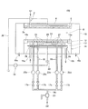
図1に、本発明の第1実施例であるウェハ処理装置100の模式的な全体図を示す。
ウェハ処理装置100は、ステージ14の表面に載置した半導体ウェハ24に対してプラズマ処理を行い、半導体ウェハ24をドライエッチングするための装置である。図1に示すように、ウェハ処理装置100は、チャンバ10と、処理ガス供給部6と、ステージ14を備えている。処理ガス供給部6とステージ14はいずれもチャンバ10内に配置されており、処理ガス供給部6とステージ14の間に放電空間8が形成されている。チャンバ10の底部には、チャンバ10内の空気を排出するためのチャンバ排気口10aが形成されている。処理ガス供給部6は、上部電極4を備えている。上部電極4は、配線30を介して接地されている。処理ガス供給部6内には、処理ガス供給路2と、複数の処理ガス供給孔2aが形成されている。処理ガス供給路2には、処理ガス供給源(図示しない)から処理ガスG1が供給される。処理ガス供給孔2aの各々は処理ガス供給路2と連通しており、その先端は放電空間8に向かって開口している。処理ガス供給源から供給された処理ガスG1は、処理ガス供給路2を経由して処理ガス供給孔2aから放電空間8へ供給される。
(First embodiment)
FIG. 1 shows a schematic overall view of a
The
ステージ14は、ステージ本体13と、絶縁部材12と、電極板(図示しない)と、枠14aと、下部電極26と、伝熱部材25を備えている。絶縁部材12と電極板は、ステージ本体13の表面に取付けられている。絶縁部材12の外周には、枠14aが取付けられている。電極板は下部電極26と導通している。下部電極26は、配線30とコンデンサ20を介して高周波電源28に接続されている。伝熱部材25はステージ本体13内の表面近傍に埋設されており、ステージ本体13よりも熱伝導率が高い材料によって形成されている。
The
ステージ本体13内には、複数のガス供給路18と、流体流路16が形成されている。複数のガス供給路18の各々は独立した流路であり、その上流端は、ガス流路18eを介してガス供給源(図示しない)に接続されている。ガス流路18eにはレギュレータ23が設けられている。レギュレータ23によって、ガス供給源から供給されるガスの圧力が所定の圧力に制御される。ガス供給路18の各々には、流量制御弁17a〜17dと圧力計22a〜22dが設けられている。流量制御弁17a〜17dは、各ガス供給路18を流れるガスの圧力を制御する。圧力計22a〜22dは、各ガス供給路18を流れるガスの圧力を検知する。流量制御弁17a〜17dと圧力計22a〜22dは制御部(図示しない)に接続されている。制御部は、圧力計22a〜22dによって検知される圧力に基づいて流量制御弁17a〜17dを制御し、各ガス供給路18を流れるガスの圧力を制御する。これによって、各ガス供給路18を流れるガス流量を独立して制御できるようになっている。
A plurality of
ガス供給路18の各々の下流端は、絶縁材料12に形成されたガス供給溝21に連通しており、ガス供給溝21の上端は放電空間8に向かって開口している。ガス供給源から供給されたガスG2は、ガス供給路18を経由してガス供給溝18aから放電空間8へ供給される。流体流路16は、ステージ本体13内を循環するように形成されている。流体流路16の一端には供給口16aが設けられ、他端には排出口16bが設けられている。供給口16aと排出口16bはステージ本体13の外側に位置している。供給口16aに供給された冷媒は、流体流路16を流れ、排出口16bから排出される。流体流路16を流れる冷媒によってステージ14が冷却され、ステージ14に載置された半導体ウェハ24も冷却される。
The downstream end of each
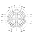
図2に、ステージ14の上視図を示す。図2は、枠14aの内側のみを示している。
図2に示すように、ステージ14は上面から視たときに円形となっている。ステージ14の表面には、ガス供給溝21a1〜21d2が形成されている。ステージ本体13の表面のうちガス供給溝21a1〜21d2が形成されていない範囲に、絶縁部材12と電極板(図示しない)が配設されている。絶縁部材12は、例えばポリイミドなどで形成されている。ステージ14は、ステージ14の周方向に4つの区画A〜Dに分割されている。区画Aの内周側にはガス供給溝21a1が形成されており、外周側にはガス供給溝21a2が形成されている。区画Bの内周側にはガス供給溝21b1が形成されており、外周側にはガス供給溝21b2が形成されている。区画Cの内周側にはガス供給溝21c1が形成されており、外周側にはガス供給溝21c2が形成されている。区画Dの内周側にはガス供給溝21d1が形成されており、外周側にはガス供給溝21d2が形成されている。各区画A〜Dの内周側に形成されているガス供給溝21a1,21b1,21c1,21d1は、円弧状に伸びる2本の溝と区画の境界線に沿って半径方向に伸びる2本の溝で構成されている。半径方向に伸びる2本の溝は、ステージ14の中央近傍で接続している。各区画A〜Dの外周側に形成されているガス供給溝21a2,21b2,21c2,21d2は、円弧状に伸びる溝で構成されている。ガス供給溝21a1〜21d2の各々は、区画A〜D毎に異なるガス供給路18に連通しており、各区画A〜Dは独立している。各ガス供給路18は、円弧状に伸びる各ガス供給溝18a1〜18d2の中央に連結している。中央に連結することで、円弧状のガスの供給溝21a1〜21d2内にガスを均等に流すことができる。ウェハ処理装置100では、各ガス供給溝18a1〜18d2のガスG2の圧力が独立して制御される。
FIG. 2 shows a top view of the
As shown in FIG. 2, the
以下に、図1、図2を参考にして、ウェハ処理装置100によって半導体ウェハ24にドライエッチングを行うときの動作の一例を説明する。
まず、ステージ14の表面に半導体ウェハ24を載置して、チャンバ10を密閉する。次に、チャンバ10内の空気をチャンバ排気口10aから排出してチャンバ10内を真空にする。次に、流体流路16に冷媒を供給する。これによって、ステージ本体13内が冷却される。
Hereinafter, an example of an operation when dry etching is performed on the
First, the
次に、ガス供給源からレギュレータ23を介してガス供給路18にガスG2を供給する。ガスG2は、例えばHeガスを用いることができる。本実施例のウェハ処理装置100では、流量制御弁17a〜17dによって、各ガス供給路18を流れるガスG2の圧力が制御される。具体的には、区画Aの内周側のガス供給溝21a1に連結されているガス供給路18a1を流れるガスの圧力が14Torr、区画Aの外周側のガス供給溝21a2に連結されているガス供給路18a2を流れるガスの圧力が12Torrに制御される。さらに、区画Bの内周側のガス供給溝21b1に連結されているガス供給路18b1を流れるガスG2の圧力が20Torr、区画Bの外周側のガス供給溝21b2に連結されているガス供給路18b2を流れるガスの圧力が18Torrに制御される。さらに、区画Cの内周側のガス供給溝21c1に連結されているガス供給路18c1を流れるガスG2の圧力が17Torr、区画Cの外周側のガス供給溝21c2に連結されているガス供給路18c2を流れるガスG2の圧力が15Torrに制御される。さらに、区画Dの内周側のガス供給溝21d1に連結されているガス供給路18d1を流れるガスG2の圧力が10Torr、区画Dの外周側のガス供給溝21d2に連結されているガス供給路18d2を流れるガスの圧力が8Torrに制御される。
Next, the gas G <b> 2 is supplied from the gas supply source to the
次に、処理ガス供給路2に処理ガスG1を供給する。処理ガス供給路2に供給された処理ガスG1は、処理ガス供給溝2aから放電空間8へ供給される。同時に、高周波電源28から下部電極26に高周波電力が印加され、下部電極26と上部電極4の間の放電空間8にグロー放電が生じる。これによって、放電空間8内の処理ガスG1がプラズマ化される。放電空間8内に発生したプラズマによって半導体ウェハ24と絶縁材料12の間に電位差が生じ、半導体ウェハ24がステージ14の表面に静電吸着される。さらに、放電空間8内に発生したプラズマによって半導体ウェハ24がドライエッチングされる。
Next, the processing gas G1 is supplied to the processing
本実施例のウェハ処理装置100では、各々のガス供給溝21a1〜21d2を流れるガスG2の圧力が制御され、半導体ウェハ24からステージ14に伝熱される熱量が制御される。ウェハ処理装置100では流体流路16を流れる冷媒によってステージ14を冷却しているため、ガス供給路18を流れるガスG2の圧力を高くすると、ステージ14によって半導体ウェハ24が冷却される効率が高くなる。また、ガス供給路18を流れるガスG2の圧力を低くすると、ステージ14によって半導体ウェハ24が冷却される効率が低くなる。このため、ガス供給溝21a1〜21d2を流れるガスG2の流量を区画A〜D毎に独立して制御することによって、半導体ウェハ24の周方向に温度の異なる4つの領域(ステージ14の区画A〜Dに対応する領域)を形成することができる。この状態でエッチングが行われるため、半導体ウェハ24に形成された温度が異なる4つの領域毎に、異なるエッチングレートでトレンチを形成することができる。これによって、半導体ウェハ24内にエッチング深さの異なる4種類のトレンチを形成することができる。なお、本実施例のウェハ処理装置100では流体流路16に流れる冷媒によってステージ14を冷却しているが、流体流路16に熱媒を流すことによってステージ14を加熱してもよい。この場合、ガス供給路18を流れるガスG2の圧力を高くすると、ステージ14によって半導体ウェハ24が加熱される効率が高くなる。ガス供給路18を流れるガスG2の圧力を低くすると、ステージ14によって半導体ウェハ24が加熱される効率が低くなる。
また、本実施例のウェハ処理装置100によると、半導体ウェハ24の周方向に複数の温度が異なる領域が形成され、各々の領域の形状が扇形となる。ウェハ処理装置100を用いて半導体ウェハ24を処理すると、半導体ウェハ24に各々の中心角が90°である扇形の領域が形成される。このため、各々の区画A〜Dの中心角を挟む2つの線分に沿って(各々の区画の境界に沿って)隙間がないようにチップパターンを形成することができる。このため、半導体ウェハ24に無駄な領域が少なくなり、チップの取れ数を十分に増やすことができる。
In the
Further, according to the
プラズマ処理によってトレンチを形成しているときの半導体ウェハ24の中央部は、外周部に比べてトレンチの表面に反応生成物が付着しやすい。このため、半導体ウェハ24の外周部はプラズマに晒されやすい。その結果、半導体ウェハの24の外周部と中央部の温度が等しければ、中央部に比べて外周部のエッチングレートが高くなり、外周部と中央部の間にエッチングばらつきが生じる。ウェハ処理装置100では、各々の区画の外周部(外側)と中央部(内側)に、独立してガスが流れるガス流路(ガス供給溝21a1〜21d2)が形成され、外周部側のガス圧力を内周部側のガス圧力より低く制御するため、ステージ14の外周部と中央部の各々でエッチングレートを制御することができる。これによって、半導体ウェハ24の外周部と中央部のエッチングレートの均一性をつくり出している。
In the central part of the
なお、ウェハ処理装置100では、ステージ本体13内の表面近傍に、各々の区画A〜Dの温度を独立して制御する冷却装置が配設されていてもよい。この場合、冷却装置を用いて各々の区画A〜D内の温度を独立して制御することができ、半導体ウェハ24の周方向に温度の異なる4つの領域(ステージ14の区画A〜Dに対応する領域)を形成することができる。また、冷却装置に替えて、各々の区画内に、区画内の温度を独立して制御する加熱装置が配設されていてもよい。
In the
また、ウェハ処理装置100では、各々の区画A〜Dの境界に沿って断熱部材が配置されていてもよい。この場合、隣接する2つの区画の間で伝熱される熱量が断熱部材によって抑制されるため、各々の区画A〜Dをより高い精度で温度制御することができる。これによって、半導体ウェハ24の周方向により高い精度で温度の異なる複数の領域を形成することができる。
In the
以上、本発明の実施例について詳細に説明したが、これらは例示に過ぎず、特許請求の範囲を限定するものではない。特許請求の範囲に記載の技術には、以上に例示した具体例を様々に変形、変更したものが含まれる。
本明細書または図面に説明した技術要素は、単独であるいは各種の組合せによって技術的有用性を発揮するものであり、出願時請求項記載の組合せに限定されるものではない。また、本明細書または図面に例示した技術は複数目的を同時に達成し得るものであり、そのうちの一つの目的を達成すること自体で技術的有用性を持つものである。
As mentioned above, although the Example of this invention was described in detail, these are only illustrations and do not limit a claim. The technology described in the claims includes various modifications and changes of the specific examples illustrated above.
The technical elements described in this specification or the drawings exhibit technical usefulness alone or in various combinations, and are not limited to the combinations described in the claims at the time of filing. In addition, the technology exemplified in this specification or the drawings can achieve a plurality of objects at the same time, and has technical usefulness by achieving one of the objects.
2:処理ガス供給路
2a:処理ガス供給孔
4:上部電極
6:処理ガス供給部
8:放電空間
10:チャンバ
10a:チャンバ排気口
12:絶縁部材
13:ステージ本体
14:ステージ
14a:枠
16:流体流路
16a;供給口
16b:排出口
17a〜17d:流量制御弁
18、18a1〜18d2:ガス供給路
18e:ガス流路
20:コンデンサ
21、21a1〜21d2:ガス供給溝
22:圧力計
23:レギュレータ
24:半導体ウェハ
25:伝熱部材
26:下部電極
28:高周波電源
30:配線
A〜D:区画
2: Process
Claims (3)
前記ステージが、そのステージの周方向に複数の区画に分割されており、
その区画の各々に、前記ステージの表面から前記半導体ウェハに伝熱される熱量を独立して制御する温度制御手段が設けられていることを特徴とするウェハ処理装置。 A wafer processing apparatus that places a semiconductor wafer on the surface of a stage and processes the semiconductor wafer,
The stage is divided into a plurality of sections in the circumferential direction of the stage;
A wafer processing apparatus, wherein a temperature control means for independently controlling the amount of heat transferred from the surface of the stage to the semiconductor wafer is provided in each of the sections.
前記温度制御手段の各々は、前記ガス流路を流れるガスの圧力を制御することを特徴とする請求項1のウェハ処理装置。 A gas flow path through which gas flows independently is formed in each of the compartments,
2. The wafer processing apparatus according to claim 1, wherein each of the temperature control means controls a pressure of a gas flowing through the gas flow path.
Priority Applications (1)
| Application Number | Priority Date | Filing Date | Title |
|---|---|---|---|
| JP2008315303A JP2010141081A (en) | 2008-12-11 | 2008-12-11 | Wafer processor |
Applications Claiming Priority (1)
| Application Number | Priority Date | Filing Date | Title |
|---|---|---|---|
| JP2008315303A JP2010141081A (en) | 2008-12-11 | 2008-12-11 | Wafer processor |
Publications (1)
| Publication Number | Publication Date |
|---|---|
| JP2010141081A true JP2010141081A (en) | 2010-06-24 |
Family
ID=42350966
Family Applications (1)
| Application Number | Title | Priority Date | Filing Date |
|---|---|---|---|
| JP2008315303A Pending JP2010141081A (en) | 2008-12-11 | 2008-12-11 | Wafer processor |
Country Status (1)
| Country | Link |
|---|---|
| JP (1) | JP2010141081A (en) |
Cited By (5)
| Publication number | Priority date | Publication date | Assignee | Title |
|---|---|---|---|---|
| WO2016067785A1 (en) * | 2014-10-30 | 2016-05-06 | 東京エレクトロン株式会社 | Substrate placing table |
| WO2017073230A1 (en) * | 2015-10-26 | 2017-05-04 | 日本発條株式会社 | Heater unit |
| CN110914971A (en) * | 2018-04-05 | 2020-03-24 | 朗姆研究公司 | Electrostatic chuck with cooling gas area and corresponding slot and monopolar electrostatic clamping electrode pattern |
| JP2020102619A (en) * | 2018-12-21 | 2020-07-02 | Toto株式会社 | Electrostatic chuck |
| WO2021240945A1 (en) * | 2020-05-25 | 2021-12-02 | 日本碍子株式会社 | Electrostatic chuck |
-
2008
- 2008-12-11 JP JP2008315303A patent/JP2010141081A/en active Pending
Cited By (33)
| Publication number | Priority date | Publication date | Assignee | Title |
|---|---|---|---|---|
| US10283398B2 (en) | 2014-10-30 | 2019-05-07 | Tokyo Electron Limited | Substrate placing table |
| US11171033B2 (en) | 2014-10-30 | 2021-11-09 | Tokyo Electron Limited | Substrate placing table |
| CN107078092B (en) * | 2014-10-30 | 2021-02-05 | 东京毅力科创株式会社 | Substrate mounting table |
| CN107078092A (en) * | 2014-10-30 | 2017-08-18 | 东京毅力科创株式会社 | Substrate-placing platform |
| WO2016067785A1 (en) * | 2014-10-30 | 2016-05-06 | 東京エレクトロン株式会社 | Substrate placing table |
| KR102093048B1 (en) | 2015-10-26 | 2020-03-24 | 닛폰 하츠죠 가부시키가이샤 | Heater unit |
| CN108141917B (en) * | 2015-10-26 | 2020-12-22 | 日本发条株式会社 | heater unit |
| US10290529B2 (en) | 2015-10-26 | 2019-05-14 | Nhk Spring Co., Ltd. | Heater unit |
| KR20180044336A (en) * | 2015-10-26 | 2018-05-02 | 닛폰 하츠죠 가부시키가이샤 | Heater unit |
| CN108141917A (en) * | 2015-10-26 | 2018-06-08 | 日本发条株式会社 | heater unit |
| WO2017073230A1 (en) * | 2015-10-26 | 2017-05-04 | 日本発條株式会社 | Heater unit |
| JP2017084523A (en) * | 2015-10-26 | 2017-05-18 | 日本発條株式会社 | Heater unit |
| US11664262B2 (en) | 2018-04-05 | 2023-05-30 | Lam Research Corporation | Electrostatic chucks with coolant gas zones and corresponding groove and monopolar electrostatic clamping electrode patterns |
| US11942351B2 (en) | 2018-04-05 | 2024-03-26 | Lam Research Corporation | Electrostatic chucks with coolant gas zones and corresponding groove and monopolar electrostatic clamping electrode patterns |
| US12237201B2 (en) | 2018-04-05 | 2025-02-25 | Lam Research Corporation | Electrostatic chucks with coolant gas zones and corresponding groove and monopolar electrostatic clamping electrode patterns |
| JP2021153202A (en) * | 2018-04-05 | 2021-09-30 | ラム リサーチ コーポレーションLam Research Corporation | Electrostatic chuck including cooling gas section, corresponding groove and unipolar electrostatic clamp electrode pattern |
| JP2020518125A (en) * | 2018-04-05 | 2020-06-18 | ラム リサーチ コーポレーションLam Research Corporation | Electrostatic chuck with cooling gas compartment and corresponding groove and unipolar electrostatic clamping electrode pattern |
| KR20200130230A (en) * | 2018-04-05 | 2020-11-18 | 램 리써치 코포레이션 | Electrostatic chucks with coolant gas zones and corresponding groove and monopolar electrostatic clamping electrode patterns |
| TWI814146B (en) * | 2018-04-05 | 2023-09-01 | 美商蘭姆研究公司 | Electrostatic chucks with coolant gas zones and corresponding groove and monopolar electrostatic clamping electrode patterns |
| KR102345663B1 (en) * | 2018-04-05 | 2021-12-29 | 램 리써치 코포레이션 | Electrostatic chucks with coolant gas zones and corresponding groove and monopolar electrostatic clamping electrode patterns |
| KR20220000955A (en) * | 2018-04-05 | 2022-01-04 | 램 리써치 코포레이션 | Electrostatic chucks with coolant gas zones and corresponding groove and monopolar electrostatic clamping electrode patterns |
| KR102543933B1 (en) * | 2018-04-05 | 2023-06-14 | 램 리써치 코포레이션 | Electrostatic chucks with coolant gas zones and corresponding groove and monopolar electrostatic clamping electrode patterns |
| JP7231669B2 (en) | 2018-04-05 | 2023-03-01 | ラム リサーチ コーポレーション | Electrostatic chuck with cooling gas compartments and corresponding grooves and monopolar electrostatic clamping electrode pattern |
| CN110914971B (en) * | 2018-04-05 | 2023-04-28 | 朗姆研究公司 | Electrostatic chuck with cooling gas region and corresponding grooves and monopolar electrostatic clamping electrode mode |
| CN110914971A (en) * | 2018-04-05 | 2020-03-24 | 朗姆研究公司 | Electrostatic chuck with cooling gas area and corresponding slot and monopolar electrostatic clamping electrode pattern |
| JP7486018B2 (en) | 2018-12-21 | 2024-05-17 | Toto株式会社 | Electrostatic Chuck |
| JP2020102619A (en) * | 2018-12-21 | 2020-07-02 | Toto株式会社 | Electrostatic chuck |
| KR20220142491A (en) * | 2020-05-25 | 2022-10-21 | 엔지케이 인슐레이터 엘티디 | electrostatic chuck |
| JPWO2021240945A1 (en) * | 2020-05-25 | 2021-12-02 | ||
| JP7356587B2 (en) | 2020-05-25 | 2023-10-04 | 日本碍子株式会社 | electrostatic chuck |
| WO2021240945A1 (en) * | 2020-05-25 | 2021-12-02 | 日本碍子株式会社 | Electrostatic chuck |
| KR102654628B1 (en) | 2020-05-25 | 2024-04-03 | 엔지케이 인슐레이터 엘티디 | electrostatic chuck |
| US12106994B2 (en) | 2020-05-25 | 2024-10-01 | Ngk Insulators, Ltd. | Electrostatic chuck |
Similar Documents
| Publication | Publication Date | Title |
|---|---|---|
| TWI725979B (en) | Susceptor and substrate processing apparatus | |
| KR102780314B1 (en) | Electrostatic chuck heater | |
| JP7090115B2 (en) | Wafer carrier with independent and isolated heater area | |
| US10622229B2 (en) | Electrostatic chuck with independent zone cooling and reduced crosstalk | |
| JP5523326B2 (en) | Electrostatic chuck assembly | |
| CN109075059B (en) | Gas distribution plate assembly for high power plasma etching processes | |
| CN102315143B (en) | Substrate processing apparatus | |
| TWI683926B (en) | Pedestal fluid-based thermal control | |
| KR102139230B1 (en) | Controlling temperature in substrate processing systems | |
| JP4990636B2 (en) | Vacuum processing equipment using a transport tray | |
| JP3742349B2 (en) | Plasma processing equipment | |
| JP2010141081A (en) | Wafer processor | |
| JP6240532B2 (en) | Electrostatic chuck temperature control method | |
| CN105590880A (en) | Reaction cavity | |
| KR101048066B1 (en) | Substrate processing apparatus | |
| JP2009016573A (en) | Electrostatic chuck and cooling method of work using the same | |
| KR102348267B1 (en) | Heating platform, thermal treatment and manufacturing method | |
| JP7356587B2 (en) | electrostatic chuck | |
| CN101419929A (en) | Electrostatic chuck | |
| JP2006245621A (en) | Plasma processing method | |
| JP2010135447A (en) | Cooling block and substrate treatment apparatus including the same | |
| JPH11170162A (en) | Surface polishing surface plate | |
| US20220002866A1 (en) | Pedestal including vapor chamber for substrate processing systems | |
| JP2011129557A (en) | Electrode plate for plasma processing apparatus |