JP6583096B2 - Distortion compensation apparatus and distortion compensation method - Google Patents
Distortion compensation apparatus and distortion compensation method Download PDFInfo
- Publication number
- JP6583096B2 JP6583096B2 JP2016069391A JP2016069391A JP6583096B2 JP 6583096 B2 JP6583096 B2 JP 6583096B2 JP 2016069391 A JP2016069391 A JP 2016069391A JP 2016069391 A JP2016069391 A JP 2016069391A JP 6583096 B2 JP6583096 B2 JP 6583096B2
- Authority
- JP
- Japan
- Prior art keywords
- frequency
- order distortion
- distortion compensation
- signal
- odd
- Prior art date
- Legal status (The legal status is an assumption and is not a legal conclusion. Google has not performed a legal analysis and makes no representation as to the accuracy of the status listed.)
- Active
Links
Images


Classifications
-
- H—ELECTRICITY
- H04—ELECTRIC COMMUNICATION TECHNIQUE
- H04B—TRANSMISSION
- H04B1/00—Details of transmission systems, not covered by a single one of groups H04B3/00 - H04B13/00; Details of transmission systems not characterised by the medium used for transmission
- H04B1/02—Transmitters
- H04B1/04—Circuits
- H04B1/0475—Circuits with means for limiting noise, interference or distortion
-
- H—ELECTRICITY
- H04—ELECTRIC COMMUNICATION TECHNIQUE
- H04B—TRANSMISSION
- H04B1/00—Details of transmission systems, not covered by a single one of groups H04B3/00 - H04B13/00; Details of transmission systems not characterised by the medium used for transmission
- H04B1/02—Transmitters
- H04B1/04—Circuits
- H04B2001/0408—Circuits with power amplifiers
- H04B2001/0425—Circuits with power amplifiers with linearisation using predistortion
Description
本発明は、歪補償装置、及び歪補償方法に関する。 The present invention relates to a distortion compensation device and a distortion compensation method.
従来、無線移動体通信の分野では、基地局等に用いられる電力増幅器の非線形歪を補償する技術が提案されている。かかる技術において、複数の周波数帯の信号を共通の電力増幅器により同時に増幅する場合、複数の歪補償部やデュアルバンドDPD(Digital Pre-Distortion)を用いて、非線形歪を補償するものがある。更に、デュアルバンドDPDを用いた信号増幅器では、二次元LUT(Look Up Table)の前段に、dual-input truncated Volterra modelのVolterraフィルタを設け、二次歪も補償するものもある。他にも、他のバンドに生じる高調波や相互変調歪を逆特性となる信号に付加することにより歪補償を行うものや、非線形連立方程式を解くことにより歪補償を行うものがある。 Conventionally, in the field of wireless mobile communication, a technique for compensating for nonlinear distortion of a power amplifier used in a base station or the like has been proposed. In such a technique, when signals of a plurality of frequency bands are simultaneously amplified by a common power amplifier, there is a technique that compensates for nonlinear distortion using a plurality of distortion compensators and dual-band DPD (Digital Pre-Distortion). Furthermore, in some signal amplifiers using dual-band DPD, a dual-input truncated Volterra model Volterra filter is provided in front of a two-dimensional LUT (Look Up Table) to compensate for second-order distortion. In addition, there are those that perform distortion compensation by adding harmonics and intermodulation distortion generated in other bands to a signal having an inverse characteristic, and those that perform distortion compensation by solving a nonlinear simultaneous equation.
しかしながら、上述した技術では、十分な歪補償性能が得られず、無線品質の低下を招いてしまうことがある。例えば、複数の周波数帯の信号を共通の電力増幅器により同時に増幅する場合を想定する。この場合、2つのバンドの中心周波数が約2倍程度の関係(例えば、4.6GHzと9GHz)にある様な条件下では、これらの中心周波数の差に相当する周波数や、低い方の中心周波数の2倍に相当する周波数において、偶数次の歪(以下、単に「偶数次歪」と記す。)が発生することがある。この様な偶数次歪が、送信信号のバンドに近い周波数に発生すると、偶数次歪をフィルタによりカットすることは困難である。また、カットするとしても、急峻なフィルタが必要となり、装置の回路規模が大きくなってしまう。特に、偶数次歪が送信信号帯域内に発生する場合には、フィルタによるカットは極めて困難となる。 However, with the above-described technology, sufficient distortion compensation performance cannot be obtained, and wireless quality may be degraded. For example, a case is assumed where signals in a plurality of frequency bands are simultaneously amplified by a common power amplifier. In this case, under conditions where the center frequencies of the two bands are about twice as high as each other (for example, 4.6 GHz and 9 GHz), the frequency corresponding to the difference between these center frequencies or the lower center frequency In some cases, even-order distortion (hereinafter, simply referred to as “even-order distortion”) may occur at a frequency corresponding to twice the above. When such even-order distortion occurs at a frequency close to the band of the transmission signal, it is difficult to cut the even-order distortion with a filter. Moreover, even if it cuts, a steep filter is needed and the circuit scale of an apparatus will become large. In particular, when even-order distortion occurs in the transmission signal band, it is extremely difficult to cut with a filter.
開示の技術は、上記に鑑みてなされたものであって、歪補償性能を向上することができる歪補償装置、及び歪補償方法を提供することを目的とする。 The disclosed technique has been made in view of the above, and an object thereof is to provide a distortion compensation apparatus and a distortion compensation method capable of improving distortion compensation performance.
上述した課題を解決し、目的を達成するために、本願の開示する歪補償装置は、一つの態様において、第1の周波数は複数の周波数を備え、増幅された信号の送信に用いる第1の周波数に発生する奇数次歪を補償する奇数次歪補償部と、第2の周波数は1以上の周波数を備え、前記信号の増幅に伴って前記第1の周波数と異なる第2の周波数に発生する偶数次歪を補償する偶数次歪補償部とを有する。 In order to solve the above-described problems and achieve the object, a distortion compensation device disclosed in the present application is, in one aspect, a first frequency having a plurality of frequencies and used for transmitting an amplified signal. An odd-order distortion compensator for compensating for odd-order distortion generated in the frequency, and the second frequency has a frequency of 1 or more, and is generated at a second frequency different from the first frequency as the signal is amplified. An even-order distortion compensator for compensating even-order distortion.
本願の開示する歪補償装置の一つの態様によれば、歪補償性能を向上することができる。 According to one aspect of the distortion compensation device disclosed in the present application, the distortion compensation performance can be improved.
以下に、本願の開示する歪補償装置、及び歪補償方法の実施例を、図面を参照しながら詳細に説明する。なお、以下の実施例により、本願の開示する歪補償装置、及び歪補償方法が限定されるものではない。 Hereinafter, embodiments of a distortion compensation device and a distortion compensation method disclosed in the present application will be described in detail with reference to the drawings. Note that the following embodiments do not limit the distortion compensation apparatus and the distortion compensation method disclosed in the present application.
図1は、本実施例に係る歪補償装置10の構成を示す図である。歪補償装置10は、複数の周波数帯域(例えば、4.6GHzと9GHz)のベースバンド信号(マルチバンド信号)を共通のアンプにより増幅する。図1に示す様に、歪補償装置10は、奇数次歪補償部11と偶数次歪補償部12とDAC(Digital to Analog Converter)13a〜13dとADC(Analog to Digital Converter)13e〜13hとアップコンバータ14a〜14dとダウンコンバータ14e〜14hと信号合成器15aと信号分配器15bとを有する。また、歪補償装置10は、アンプ16とカップラ17と奇数次歪補償係数更新部18と偶数次歪補償係数更新部19とを有する。これら各構成部分は、一方向又は双方向に、各種信号やデータの入出力が可能な様に接続されている。
FIG. 1 is a diagram illustrating a configuration of a
以下では、バンドA(中心周波数fA)及びバンドB(中心周波数fB)のデュアルバンド信号を、共通増幅(fA<fB)する場合を例にとり説明する。奇数次歪補償部11は、バンドAの送信信号xA(n)とバンドBの送信信号xB(n)との2つの信号を入力し、該信号に基づき、バンドA(中心周波数fA)の奇数次歪補償信号とバンドB(中心周波数fB)の奇数次歪補償信号とを生成する。同様に、偶数次歪補償部12は、バンドAの送信信号xA(n)とバンドBの送信信号xB(n)との2つの信号を入力し、該信号に基づき、中心周波数fC=2fAの偶数次歪補償信号と中心周波数fD=fB−fAの偶数次歪補償信号とを生成する。DAC13a、13bは、奇数次歪補償部11から入力される奇数次歪補償信号の各々をデジタル信号からアナログ信号に変換する。同様に、DAC13c、13dは、偶数次歪補償部12から入力される偶数次歪補償信号の各々をデジタル信号からアナログ信号に変換する。
In the following, a case where dual band signals of band A (center frequency f A ) and band B (center frequency f B ) are commonly amplified (f A <f B ) will be described as an example. The odd-
アップコンバータ14a〜14dは、対応するDAC13a〜13dから入力されるアナログ信号を、それぞれ周波数fA、fB、fC=2fA、fD=fB−fAへ周波数変換し、RF(Radio Frequency)信号を生成する。信号合成器15aは、アップコンバータ14a〜14dから入力されるRF信号の各々を合成する。アンプ16は、信号合成器15aから入力される合成後の信号を電力増幅する。カップラ17は、アンプ16から入力される信号を分配した後、一方の信号をアンテナA1から無線送信し、他方の信号を信号分配器15bにフィードバックする。
The up-
信号分配器15bは、フィードバックされる上記信号を4つの信号に分配する。ダウンコンバータ14e〜14hは、信号分配器15bから入力される信号を、それぞれ周波数fA、fB、fC=2fA、fD=fB−fAからベースバンドへ周波数変換する。ADC13e〜13hは、対応するダウンコンバータ14e〜14hから入力されるアナログ信号の各々を、デジタル信号に変換する。
The
奇数次歪補償係数更新部18は、バンドAの送信信号xA(n)とバンドBの送信信号xB(n)とバンドA(中心周波数fA)のフィードバック信号とバンドB(中心周波数fB)のフィードバック信号と更新前の歪補償係数とに基づき、奇数次歪補償係数を更新する。奇数次歪補償係数更新部18は、更新後の奇数次歪補償係数を奇数次歪補償部11へ出力する。同様に、偶数次歪補償係数更新部19は、バンドAの送信信号xA(n)とバンドBの送信信号xB(n)と中心周波数fC=2fAのフィードバック信号と中心周波数fD=fB−fAのフィードバック信号と更新前の歪補償係数とに基づき、偶数次歪補償係数を更新する。偶数次歪補償係数更新部19は、更新後の偶数次歪補償係数を偶数次歪補償部12へ出力する。
The odd-order distortion compensation
図2は、本実施例に係る奇数次歪補償部11及び偶数次歪補償部12の構成を示す図である。図2に示す様に、奇数次歪補償部11は、振幅算出部11a、11bと、アドレス生成部11c、11dと、LUT11e、11fと、複素乗算器11g、11hとを有する。偶数次歪補償部12は、複素乗算器12aと、複素共役算出部12bと、複素乗算器12cと、LUT12d、12eと、複素乗算器12f、12gとを有する。これら各構成部分は、一方向又は双方向に、各種信号やデータの入出力が可能な様に接続されている。
FIG. 2 is a diagram illustrating a configuration of the odd-order
振幅算出部11a、11bは、バンドAの送信信号xA(n)の振幅とバンドBの送信信号xB(n)の振幅とをそれぞれ算出する。アドレス生成部11c、11dは、算出された振幅の情報をそれぞれアドレスに変換し、これら2つのアドレスを4つのLUT11e、11f、12d、12eへ出力する。LUT11e、11fは、歪補償係数をアドレスと対応付けて更新可能なメモリに格納する。複素乗算器11gは、上記2つのアドレスに基づき、バンドA(中心周波数fA)の奇数次歪補償用のLUT11eから、バンドAの奇数次歪補償係数を読み出して、バンドAの送信信号xA(n)と複素乗算し、バンドAの奇数次歪補償信号yA(n)を生成する。複素乗算器11hは、上記2つのアドレスに基づき、バンドB(中心周波数fB)の奇数次歪補償用のLUT11fから、バンドBの奇数次歪補償係数を読み出して、バンドBの送信信号xB(n)と複素乗算し、バンドBの奇数次歪補償信号yB(n)を生成する。
The
複素乗算器12aは、バンドAの送信信号xA(n)を二乗し、中心周波数fC=2fAの偶数次歪の元になる信号xC(n)を生成する。複素共役算出部12bは、バンドAの送信信号xA(n)の複素共役を算出する。複素乗算器12cは、算出された複素共役と、バンドBの送信信号xB(n)とを複素乗算し、中心周波数fD=fB−fAの偶数次歪の元になる信号xD(n)を生成する。LUT12d、12eは、歪補償係数をアドレスと対応付けて更新可能なメモリに格納する。複素乗算器12fは、上記2つのアドレスに基づき、中心周波数fC=2fAの偶数次歪補償用のLUT12dから、中心周波数fC=2fAの偶数次歪補償係数を読み出して、中心周波数fC=2fAの偶数次歪の元になる信号xC(n)と複素乗算し、中心周波数fC=2fAの偶数次歪補償信号yC(n)を生成する。複素乗算器12gは、上記2つのアドレスに基づき、中心周波数fD=fB−fAの偶数次歪補償用のLUT12eから、中心周波数fD=fB−fAの偶数次歪補償係数を読み出して、中心周波数fD=fB−fAの偶数次歪の元になる信号xD(n)と複素乗算し、中心周波数fD=fB−fAの偶数次歪補償信号yD(n)を生成する。
The complex multiplier 12a squares the transmission signal x A (n) of the band A, and generates a signal x C (n) that is a source of even-order distortion of the center frequency f C = 2f A. The complex
図3は、本実施例に係る奇数次歪補償係数更新部18及び偶数次歪補償係数更新部19の構成を示す図である。図3に示す様に、奇数次歪補償係数更新部18は、減算器18aと、複素共役算出部18bと、更新部18cと、減算器18dと、複素共役算出部18eと、更新部18fとを有する。偶数次歪補償係数更新部19は、複素乗算器19aと、複素共役算出部19bと、複素乗算器19cと、複素共役算出部19dと、更新部19eと、複素共役算出部19fと、更新部19gとを有する。これら各構成部分は、一方向又は双方向に、各種信号やデータの入出力が可能な様に接続されている。
FIG. 3 is a diagram illustrating a configuration of the odd-order distortion compensation
減算器18aは、バンドA(中心周波数fA)のフィードバック信号zA(n)とバンドAの送信信号xA(n)との誤差を算出し、バンドAの誤差信号eA(n)=xA(n)−zA(n)を得る。複素共役算出部18bは、バンドAの送信信号xA(n)の複素共役を算出する。更新部18cは、上記誤差信号eA(n)と、上記複素共役と、LUT11eから取得(nA−2)された更新前のバンドAの奇数次歪補償係数とを用いて、バンドAの奇数次歪補償係数wA(|xA(n)|,|xB(n)|)を更新する。更新後の奇数次歪補償係数の値は、LUT11eに格納される。
The
同様に、減算器18dは、バンドB(中心周波数fB)のフィードバック信号zB(n)とバンドBの送信信号xB(n)との誤差を算出し、バンドBの誤差信号eB(n)=xB(n)−zB(n)を得る。複素共役算出部18eは、バンドBの送信信号xB(n)の複素共役を算出する。更新部18fは、上記誤差信号eB(n)と、上記複素共役と、LUT11fから取得(nB−2)された更新前のバンドBの奇数次歪補償係数とを用いて、バンドBの奇数次歪補償係数wB(|xA(n)|,|xB(n)|)を更新する。更新後の奇数次歪補償係数の値は、LUT11fに格納される。
Similarly, the subtractor 18d calculates an error between the feedback signal z B (n) of the band B (center frequency f B ) and the transmission signal x B (n) of the band B, and an error signal e B ( n) = x B (n) −z B (n) is obtained. The complex conjugate calculation unit 18e calculates the complex conjugate of the transmission signal x B (n) of band B. The
複素乗算器19aは、バンドAの送信信号xA(n)を二乗し、中心周波数fC=2fAの偶数次歪の元になる信号xC(n)={xA(n)}2を生成する。複素共役算出部19bは、バンドAの送信信号xA(n)の複素共役を算出する。複素乗算器19cは、上記複素共役とバンドBの送信信号xB(n)とを複素乗算し、中心周波数fD=fB−fAの偶数次歪の元になる信号xD(n)={xA(n)}*xB(n)を生成する。
The
複素共役算出部19dは、中心周波数fC=2fAの偶数次歪の元になる信号xC(n)の複素共役を算出する。更新部19eは、中心周波数fC=2fAの偶数次歪の誤差信号eC(n)と、上記複素共役と、LUT12dから取得(nC−2)された更新前の中心周波数fC=2fAの偶数次歪補償係数とを用いて、中心周波数fC=2fAの偶数次歪補償係数wC(|xA(n)|,|xB(n)|)を更新する。更新後の偶数次歪補償係数の値は、LUT12dに格納される。ここで、誤差信号eC(n)は、中心周波数fC=2fAの偶数次歪のフィードバック信号zC(n)とゼロ信号との誤差を示す信号であり、本実施例では、誤差信号eC(n)=−zC(n)となる。 The complex conjugate calculator 19d calculates the complex conjugate of the signal x C (n) that is the source of the even-order distortion having the center frequency f C = 2f A. The update unit 19e includes an even-order distortion error signal e C (n) having a center frequency f C = 2f A , the complex conjugate, and the center frequency f C before update acquired from the LUT 12d (n C-2 ). by using the even-order distortion compensation coefficient of 2f a, center frequency f C = 2f a of even-order distortion compensation coefficient w C (| x a (n ) |, | x B (n) |) update. The updated even-order distortion compensation coefficient value is stored in the LUT 12d. Here, the error signal e C (n) is a signal indicating an error between the even-order distortion feedback signal z C (n) having the center frequency f C = 2f A and the zero signal. In this embodiment, the error signal e C (n) is an error signal. e C (n) = − z C (n).
同様に、複素共役算出部19fは、中心周波数fD=fB−fAの偶数次歪の元になる信号xD(n)の複素共役を算出する。更新部19gは、中心周波数fD=fB−fAの偶数次歪の誤差信号eD(n)と、上記複素共役と、LUT12eから取得(nD−2)された更新前の中心周波数fD=fB−fAの偶数次歪補償係数とを用いて、中心周波数fD=fB−fAの偶数次歪補償係数wD(|xA(n)|,|xB(n)|)を更新する。更新後の偶数次歪補償係数の値は、LUT12eに格納される。ここで、誤差信号eD(n)は、中心周波数fD=fB−fAの偶数次歪のフィードバック信号zD(n)とゼロ信号との誤差を示す信号であり、本実施例では、誤差信号eD(n)=−zD(n)となる。 Similarly, the complex conjugate calculation unit 19f calculates the complex conjugate of the center frequency f D = f B -f underlying even order distortion of the A signal x D (n). The update unit 19g obtains the even-order distortion error signal e D (n) of the center frequency f D = f B −f A , the complex conjugate, and the center frequency before update acquired from the LUT 12e (n D−2 ). by using the even-order distortion compensation coefficient f D = f B -f a, center frequency f D = f B -f a of even-order distortion compensation coefficient w D (| x a (n ) |, | x B ( n) Update |). The updated even-order distortion compensation coefficient value is stored in the LUT 12e. Here, the error signal e D (n) is a signal indicating an error between the center frequency f D = f B -f even-order distortion feedback signal z D (n) and the zero signal of the A, in this example , Error signal e D (n) = − z D (n).
以下、バンドA(中心周波数fA)及びバンドB(中心周波数fB)のデュアルバンド信号を、共通増幅(fA<fB)する場合を例にとり、偶数次歪を補償する方法について、より具体的に説明する。上述した様に、歪補償装置10は、信号の共通増幅時に、奇数次歪を補償する歪補償部と偶数次歪を補償する歪補償部との両方を備える構成を採る。歪補償装置10は、奇数次歪を補償する際、バンドAに対しては、バンドAの送信信号とバンドA、Bの振幅情報(更新後の歪補償係数)とを用い、バンドBに対しては、バンドBの送信信号とバンドA、Bの振幅情報(更新後の歪補償係数)とを用いる。これに対して、歪補償装置10は、中心周波数fevenに発生する偶数次歪を補償する際、下記の偶数次歪信号(偶数次項)とバンドA、Bの振幅情報(更新後の歪補償係数)とを用いる。なお、振幅情報は、LUT11e、11f、12d、12eから歪補償係数を特定するためのアドレスとして用いられる。
A method for compensating even-order distortion will be described below, taking as an example a case where dual band signals of band A (center frequency f A ) and band B (center frequency f B ) are subjected to common amplification (f A <f B ). This will be specifically described. As described above, the
偶数次歪の中心周波数feven=a×fA+b×fB(但し、a、bは整数、a+bは偶数)とすると、上記の偶数次歪信号(偶数次項)は、a、bの値に応じて、以下の様に表すことができる。なお、^は累乗を表す。
1.a≧0かつb≧0が成立する場合、
(バンドAの送信信号)^|a|×(バンドBの送信信号)^|b|
2.a≧0かつb<0が成立する場合、
(バンドAの送信信号)^|a|×(バンドBの送信信号の複素共役)^|b|
3.a<0かつb≧0が成立する場合、
(バンドAの送信信号の複素共役)^|a|×(バンドBの送信信号)^|b|
4.a<0かつb<0が成立する場合、
(バンドAの送信信号の複素共役)^|a|×(バンドBの送信信号の複素共役)^|b|
The center frequency f of the even order distortion even = a × f A + b × f B ( where, a, b are integers, a + b is an even number) when to the above even-order distortion signals (even below) may, a, b values Can be expressed as follows. Note that ^ represents a power.
1. When a ≧ 0 and b ≧ 0 hold,
(Band A transmission signal) ^ | a | × (band B transmission signal) ^ | b |
2. If a ≧ 0 and b <0 hold,
(Band A transmission signal) ^ | a | × (complex conjugate of band B transmission signal) ^ | b |
3. When a <0 and b ≧ 0 hold,
(Complex conjugate of transmission signal of band A) ^ | a | × (transmission signal of band B) ^ | b |
4). If a <0 and b <0 hold,
(Complex conjugate of transmission signal of band A) ^ | a | × (complex conjugate of transmission signal of band B) ^ | b |
図4は、歪補償を行わない場合における共通増幅時のアンプ入力及びアンプ出力のスペクトラムを示す図である。図4では、横軸に周波数が規定され、縦軸に電力が規定されている。図4に示す様に、歪補償を行わない場合、太線に示すアンプ入力は、アンプ出力段階では、4つの周波数fA〜fDにおいて歪が発生する。すなわち、中心周波数fA(バンドA)及び中心周波数fB(バンドB)では、奇数次歪が発生するため、隣接チャネルへの漏洩電力が増大してしまう。中心周波数fC=2fA(a=2、b=0)及び中心周波数fD=fB−fA(a=−1、b=1)では、偶数次歪が発生するため、周波数fC、fDへの漏洩電力が増大してしまう。 FIG. 4 is a diagram illustrating a spectrum of amplifier input and amplifier output during common amplification when distortion compensation is not performed. In FIG. 4, the horizontal axis defines the frequency, and the vertical axis defines the power. As shown in FIG. 4, when distortion compensation is not performed, the amplifier input indicated by the thick line is distorted at four frequencies f A to f D at the amplifier output stage. That is, since odd-order distortion occurs at the center frequency f A (band A) and the center frequency f B (band B), the leakage power to the adjacent channel increases. At the center frequency f C = 2f A (a = 2, b = 0) and the center frequency f D = f B −f A (a = −1, b = 1), even-order distortion occurs, so the frequency f C , F D leakage power increases.
従って、例えば、中心周波数fC=2fA(a=2、b=0)では、a≧0かつb≧0が成立するため、偶数次歪信号(偶数次項)は、(バンドAの送信信号)^|a|×(バンドBの送信信号)^|b|により、{xA(n)}2となる。また、例えば、中心周波数fD=fB−fA(a=−1、b=1)では、a<0かつb≧0が成立するため、偶数次歪信号(偶数次項)は、(バンドAの送信信号の複素共役)^|a|×(バンドBの送信信号)^|b|により、{xA(n)}*xB(n)となる。 Therefore, for example, at the center frequency f C = 2f A (a = 2, b = 0), since a ≧ 0 and b ≧ 0, the even-order distortion signal (even-order term) is (the transmission signal of band A). ) ^ | A | × (band B transmission signal) ^ | b |, {x A (n)} 2 Further, for example, at the center frequency f D = f B −f A (a = −1, b = 1), a <0 and b ≧ 0 are satisfied, so that the even-order distortion signal (even-order term) is (band) {Complex conjugate of transmission signal of A) ^ | a | × (transmission signal of band B) ^ | b |, {x A (n)} * x B (n).
その結果、歪補償処理後の信号yA(n)、yB(n)、yC(n)、yD(n)は、それぞれ以下の数式(1)〜(4)により、表すことができる(但し、wA、wB、wC、wDは歪補償係数)。

また、ダイレクトラーニング方式を用いる場合、奇数次歪補償部11は、それぞれ以下の数式(5)、(6)の様に、奇数次歪の補償係数の更新を行う。同様に、ダイレクトラーニング方式を用いる場合、偶数次歪補償部12は、それぞれ以下の数式(7)、(8)の様に、偶数次歪の補償係数の更新を行う。
また、誤差信号eA(n)、eB(n)、eC(n)、eD(n)は、それぞれ以下の数式(9)〜(12)により、表すことができる(但し、zA(n)、zB(n)、zC(n)、zD(n)はフィードバック信号)。
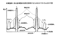
図5は、本実施例に係る歪補償の効果を説明するためのスペクトラムを示す図である。図5では、横軸に周波数が規定され、縦軸に電力が規定されている。図5に示す様に、歪補償の無い場合には、中心周波数fA(バンドA)及び中心周波数fB(バンドB)において、奇数次歪が発生し、中心周波数fC及び中心周波数fDにおいて、偶数次歪が発生する。本実施例に係る歪補償技術の適用により、スペクトラムは、太線に示す様に変化する。すなわち、奇数次歪が補償されるだけでなく、偶数次歪も、高精度に補償可能となる。 FIG. 5 is a diagram illustrating a spectrum for explaining the effect of distortion compensation according to the present embodiment. In FIG. 5, the horizontal axis defines the frequency, and the vertical axis defines the power. As shown in FIG. 5, when there is no distortion compensation, odd-order distortion occurs at the center frequency f A (band A) and the center frequency f B (band B), and the center frequency f C and the center frequency f D. In this case, even-order distortion occurs. By applying the distortion compensation technique according to the present embodiment, the spectrum changes as shown by a thick line. That is, not only the odd-order distortion is compensated but also the even-order distortion can be compensated with high accuracy.
以上説明した様に、歪補償装置10は、奇数次歪補償部11と偶数次歪補償部12とを有する。奇数次歪補償部11は、第1の周波数は複数の周波数を備え、増幅された信号の送信に用いる第1の周波数に発生する奇数次歪を補償する。偶数次歪補償部12は、第2の周波数は1以上の周波数を備え、上記信号の増幅に伴って上記第1の周波数と異なる第2の周波数に発生する偶数次歪を補償する。より具体的には、奇数次歪補償部11は、信号を増幅して送信する際に該信号の送信に用いる該信号近傍の第1及び第2の周波数(例えば、fA、fB)に発生する奇数次歪を補償する。偶数次歪補償部12は、上記信号の増幅に伴って第3及び第4の周波数(例えば、fC=2fA、fD=fB−fA)に発生する偶数次歪を補償する。
As described above, the
歪補償装置10において、奇数次歪補償部11は、上記第1の周波数に、対応する周波数の送信信号と、対応する周波数の奇数次歪補償係数とを用いて、奇数次歪補償後の信号を生成するものとしてもよい。偶数次歪補償部12は、上記第2の周波数に、上記第1の周波数の送信信号と、上記第2の周波数の偶数次歪補償係数とを用いて、偶数次歪補償後の信号を生成するものとしてもよい。より具体的には、歪補償装置10において、奇数次歪補償部11は、上記第1及び第2の周波数毎に、対応する周波数の送信信号(例えば、数式(1)のxA(n)、数式(2)のxB(n))と、対応する周波数の奇数次歪補償係数(例えば、wA(|xA(n)|,|xB(n)|)、wB(|xA(n)|,|xB(n)|))とを用いて、奇数次歪補償後の信号(例えば、yA(n)、yB(n))を生成するものとしてもよい。また、偶数次歪補償部12は、上記第3及び第4の周波数毎に、上記第1の周波数の送信信号(例えば、数式(3)の{xA(n)}2、数式(4)の{xA(n)}*)と、対応する周波数の偶数次歪補償係数(例えば、wC(|xA(n)|,|xB(n)|)、wD(|xA(n)|,|xB(n)|))とを用いて、偶数次歪補償後の信号(例えば、yC(n)、yD(n))を生成するものとしてもよい。
In the
歪補償装置10において、偶数次歪補償部12は、上記第2の周波数が、上記第1の周波数の2倍である場合には、上記第1の周波数の送信信号を2乗した値と、上記第2の周波数の偶数次歪補償係数とを用いて、偶数次歪補償後の信号を生成するものとしてもよい。また、偶数次歪補償部12は、上記第2の周波数が、上記第1の周波数の備える上記複数の周波数間の差である場合には、上記第1の周波数の送信信号の複素共役と、上記第1の周波数の送信信号と、上記第2の周波数の偶数次歪補償係数とを用いて、偶数次歪補償後の信号を生成するものとしてもよい。より具体的には、歪補償装置10において、偶数次歪補償部12は、上記第3の周波数が、上記第1の周波数の2倍である場合(例えば、fC=2fA)には、上記第1の周波数の送信信号を2乗した値(例えば、数式(3)の{xA(n)}2)と、上記第3の周波数の偶数次歪補償係数(例えば、wC(|xA(n)|,|xB(n)|))とを用いて、上記第3の周波数に生じる歪を補償した偶数次歪補償後の信号を生成するものとしてもよい。また、偶数次歪補償部12は、上記第4の周波数が、上記第2の周波数と上記第1の周波数との差である場合(例えば、fD=fB−fA)には、上記第1の周波数の送信信号の複素共役(例えば、数式(4)の{xA(n)}*)と、上記第2の周波数の送信信号(例えば、xB(n))と、上記第4の周波数の偶数次歪補償係数(例えば、wD(|xA(n)|,|xB(n)|))とを用いて、上記第4の周波数に生じる歪を補償した偶数次歪補償後の信号を生成するものとしてもよい。
In the
歪補償装置10において、上記第1の周波数に、対応する周波数の送信信号とフィードバック信号との差分である誤差信号と、対応する周波数の送信信号の複素共役とを用いて、上記奇数次歪補償係数を更新する奇数次歪補償係数更新部18を更に有するものとしてもよい。また、上記第2の周波数に、ゼロ信号とフィードバック信号との差分である誤差信号と、対応する周波数の偶数次歪の元になる信号の複素共役とを用いて、上記偶数次歪補償係数を更新する偶数次歪補償係数更新部19を更に有するものとしてもよい。より具体的には、歪補償装置10において、上記第1及び第2の周波数毎に、対応する周波数の送信信号とフィードバック信号(例えば、zA(n)、zB(n))との差分である誤差信号(例えば、eA(n)、eB(n))と、対応する周波数の送信信号の複素共役(例えば、{xA(n)}*、{xB(n)}*)とを用いて、上記奇数次歪補償係数を更新する奇数次歪補償係数更新部18を更に有するものとしてもよい。また、上記第3及び第4の周波数毎に、ゼロ信号とフィードバック信号(例えば、zC(n)、zD(n))との差分である誤差信号(例えば、eC(n)、eD(n))と、対応する周波数の偶数次歪の元になる信号の複素共役(例えば、{xC(n)}*、{xD(n)}*)とを用いて、上記偶数次歪補償係数を更新する偶数次歪補償係数更新部19を更に有するものとしてもよい。
In the
(変形例1)
上記実施例では、LUTを用いたLUT型歪補償を例示したが、級数型歪補償を用いることもできる。級数型歪補償では、歪補償装置10は、歪補償方式として、PA(Power Amplifier)の非線形歪の逆特性を「べき級数」により近似し、べき級数を用いて歪補償を行う。具体的には、歪補償装置10は、入力されたベースバンド信号に対して、高次の信号を複数生成し、次数毎に用意された歪補償係数を高次の各信号に乗算し、歪補償係数乗算後の全ての信号を合成して歪補償信号を生成する。
(Modification 1)
In the above embodiment, the LUT type distortion compensation using the LUT is exemplified, but the series type distortion compensation can also be used. In series distortion compensation, the
(変形例2)
上記実施例では、図1〜図3に示す様に、歪補償装置10は、アップコンバータ14a〜14d及びダウンコンバータ14e〜14hの各々に、局部発振器を用いるものとした。しかしながら、かかる態様に限らず、歪補償装置10は、アップコンバータ14c、14dにそれぞれ入力される周波数fC=2fA及びfD=fB−fAのローカル信号を、周波数fA及び周波数fBのローカル信号からミキサを用いてミキシング生成するものとしてもよい。同様に、歪補償装置10は、ダウンコンバータ14g、14hにそれぞれ入力される周波数fC=2fA及びfD=fB−fAのローカル信号を、周波数fA及び周波数fBのローカル信号からミキサを用いてミキシング生成するものとしてもよい。これにより、局部発振器の個数を減らすこと(例えば、4個から2個)ができる。
(Modification 2)
In the above embodiment, as shown in FIGS. 1 to 3, the
(変形例3)
上記実施例では、図1、図2に示す様に、DACが4つの場合を例示したが、1つの高速DACによる構成も可能である。すなわち、DACの信号処理帯域が、奇数次歪の帯域(中心周波数fA、fB)と偶数次歪の帯域(中心周波数fC=2fA、fD=fB−fA)との全てをカバーできる程度に広帯域である場合には、歪補償装置10は、DACを共通化する構成を採ることができる。かかる態様では、歪補償装置10は、デジタル領域において、中心周波数fA、fBの奇数次歪補償信号yA(n)、yB(n)と、中心周波数fC、fDの偶数次歪補償信号yC(n)、yD(n)とを、それぞれ中間周波数にデジタルアップコンバートする。歪補償装置10は、これらの歪補償信号yA(n)〜yD(n)を、デジタルの信号合成器により合成した後、共通のDACにおいてデジタル信号からアナログ信号に変換し、共通のアップコンバータにおいて無線周波数にアップコンバートする。これにより、DACの個数を減らすこと(例えば、4個から1個)ができる。
(Modification 3)
In the above embodiment, as shown in FIGS. 1 and 2, the case where there are four DACs is illustrated, but a configuration with one high-speed DAC is also possible. That is, the DAC signal processing band includes all of odd-order distortion bands (center frequencies f A and f B ) and even-order distortion bands (center frequencies f C = 2f A and f D = f B −f A ). When the bandwidth is wide enough to cover, the
更に、バンドA、B(中心周波数fA、fB)が十分に低周波であり、かつ、DACの信号処理帯域が、奇数次歪の帯域(中心周波数fA、fB)と偶数次歪の帯域(中心周波数fC=2fA、fD=fB−fA)との全てをカバーできる場合には、歪補償装置10は、それ程高速でない汎用DACを用いても、同様の構成(DACが1つの構成)を採ることができる。
Furthermore, the bands A and B (center frequencies f A and f B ) are sufficiently low, and the DAC signal processing band is an odd-order distortion band (center frequencies f A and f B ) and an even-order distortion. In the case of using a general-purpose DAC that is not so fast, the
(変形例4)
上記実施例では、図1、図3に示す様に、ADCが4つの場合を例示したが、1つの高速ADCによる構成も可能である。すなわち、ADCの信号処理帯域が、奇数次歪の帯域(中心周波数fA、fB)と偶数次歪の帯域(中心周波数fC=2fA、fD=fB−fA)との全てをカバーできる程度に広帯域である場合には、歪補償装置10は、ADCを共通化する構成を採ることができる。かかる態様では、歪補償装置10は、共通のダウンコンバータにおいて中間周波数にダウンコンバートし、共通のADCにおいてアナログ信号からデジタル信号に変換した後、デジタルの信号分配器により分配を行う。歪補償装置10は、デジタル領域において、中心周波数fA、fBの奇数次歪のフィードバック信号zA(n)、zB(n)と、中心周波数fC、fDの偶数次歪のフィードバック信号zC(n)、zD(n)とを、それぞれ中間周波数からベースバンドへデジタルダウンコンバートし、フィルタ処理を施す。これにより、ADCの個数を減らすこと(例えば、4個から1個)ができる。
(Modification 4)
In the above embodiment, as shown in FIGS. 1 and 3, the case where there are four ADCs is illustrated, but a configuration with one high-speed ADC is also possible. That is, the ADC signal processing bands are all odd-order distortion bands (center frequencies f A , f B ) and even-order distortion bands (center frequencies f C = 2f A , f D = f B −f A ). If the bandwidth is wide enough to cover, the
更に、バンドA、B(中心周波数fA、fB)が十分に低周波であり、かつ、ADCの信号処理帯域が、奇数次歪の帯域(中心周波数fA、fB)と偶数次歪の帯域(中心周波数fC=2fA、fD=fB−fA)との全てをカバーできる場合には、歪補償装置10は、それ程高速でない汎用ADCを用いても、同様の構成(ADCが1つの構成)を採ることができる。 Furthermore, the bands A and B (center frequencies f A and f B ) are sufficiently low, and the ADC signal processing band is an odd-order distortion band (center frequencies f A and f B ) and an even-order distortion. In the case of using a general-purpose ADC that is not so high speed (the center frequency f C = 2f A , f D = f B −f A ). The ADC can take one configuration).
(変形例5)
偶数次歪が送信信号の近傍に発生する場合にも、DAC及びADCを共通化した構成を採ることができる。図6は、変形例5に係るスペクトラムとDAC及びADCの信号処理帯域との関係を示す図である。図6に示す様に、奇数次歪のバンドA(中心周波数fA)と、偶数次歪の中心周波数fD=fB−fAとが近く、DAC及びADCの信号処理帯域が、これら双方の周波数帯域をカバーすることができる場合には、歪補償装置10は、DAC及びADCを共通化した構成を採るものとしてもよい。同様に、図6に示す様に、奇数次歪のバンドB(中心周波数fB)と、偶数次歪の中心周波数fC=2fAとが近く、DAC及びADCの信号処理帯域が、これら双方の周波数帯域をカバーすることができる場合には、歪補償装置10は、DAC及びADCを共通化した構成を採るものとしてもよい。
(Modification 5)
Even when even-order distortion occurs in the vicinity of the transmission signal, a configuration in which the DAC and the ADC are shared can be employed. FIG. 6 is a diagram illustrating a relationship between the spectrum according to the fifth modification and the signal processing bands of the DAC and the ADC. As shown in FIG. 6, the odd-order distortion band A (center frequency f A ) and the even-order distortion center frequency f D = f B −f A are close, and the signal processing bands of the DAC and ADC are both When the frequency band can be covered, the
図7は、変形例5に係る歪補償装置10の構成を示す図である。図7では、図1と共通する構成要素には、同一の参照符号を用いると共に、その詳細な説明は省略する。図7に示す様に、アップコンバータ14a−1、14dは、デジタル領域において、バンドA(中心周波数fA)の奇数次歪補償信号yA(n)を、周波数f’A=fA−fB/2に、中心周波数fDの偶数次歪補償信号yD(n)を、周波数f’D=fB/2−fAにそれぞれ周波数変換する。信号合成器15a−1は、周波数変換された歪補償信号yA(n)、yD(n)をデジタル合成する。DAC13aは、合成後の信号を、デジタル信号からアナログ信号に変換する。共通のアップコンバータ14a−2は、該アナログ信号を、ローカル周波数fL1=fB/2により、無線周波数にアップコンバートする。
FIG. 7 is a diagram illustrating a configuration of the
アップコンバータ14b、14c−1は、デジタル領域において、バンドB(中心周波数fB)の奇数次歪補償信号yB(n)を、周波数f’B=fB/2−fAに、中心周波数fCの偶数次歪補償信号yC(n)を、周波数f’C=fA−fB/2にそれぞれ周波数変換する。信号合成器15a−2は、周波数変換された歪補償信号yB(n)、yC(n)をデジタル合成する。DAC13cは、合成後の信号を、デジタル信号からアナログ信号に変換する。共通のアップコンバータ14c−2は、該アナログ信号を、ローカル周波数fL2=fA+fB/2により、無線周波数にアップコンバートする。アップコンバータ14a−2、14c−2からそれぞれ出力された無線周波数(RF)信号は、信号合成器15a−3により合成された後、アンプ16により電力増幅される。
In the digital domain, the up-
信号分配器15b−1は、フィードバック信号を2つに分配し、2つのダウンコンバータ14e−1、14g−1に出力する。2つのダウンコンバータ14e−1、14g−1は、入力された上記フィードバック信号を、対応するローカル周波数fL1=fB/2、fL2=fA+fB/2により、それぞれ周波数変換する。2つのADC13e、13gは、周波数変換されたアナログ信号を、それぞれデジタル信号に変換する。信号分配器15b−2は、ADC13eからのADC出力信号を分配し、ダウンコンバータ14e−2、14hにそれぞれ出力する。ダウンコンバータ14e−2、14hは、バンドA(中心周波数fA)の奇数次歪のフィードバック信号zA(n)を、周波数f’A=fA−fB/2からベースバンドに、中心周波数fDの偶数次歪のフィードバック信号zD(n)を、周波数f’D=fB/2−fAからベースバンドに、それぞれ周波数変換し、フィルタ処理を施す。信号分配器15b−3は、ADC13gからのADC出力信号を分配し、ダウンコンバータ14f、14g−2にそれぞれ出力する。ダウンコンバータ14f、14g−2は、バンドB(中心周波数fB)の奇数次歪のフィードバック信号zB(n)を、周波数f’B=fB/2−fAからベースバンドに、中心周波数fCの偶数次歪のフィードバック信号zC(n)を、周波数f’C=fA−fB/2からベースバンドに、それぞれ周波数変換し、フィルタ処理を施す。
The
変形例5に係る歪補償装置10によれば、アナログ回路部の部品点数を減らすことができる。
According to the
なお、上述の実施例では、信号送信に用いる周波数帯域として、2つの帯域(例えば、4.6GHzと9GHz)を例示したが、歪補償装置10を有する基地局等が、1つまたは3つ以上の帯域を用いて、信号を送信するものとしてもよい。同様に、偶数次歪を抑制する帯域についても、2つの帯域に限らず、1つまたは3つ以上の帯域であってもよい。また、奇数次歪の発生する周波数帯域と、偶数次歪の発生する周波数帯域とは、必ずしも異なる帯域でなくてもよい。
In the above-described embodiment, two bands (for example, 4.6 GHz and 9 GHz) are illustrated as frequency bands used for signal transmission. However, one or three or more base stations having the
また、歪補償装置10の各構成要素は、必ずしも物理的に図示の如く構成されていることを要しない。すなわち、各装置の分散・統合の具体的態様は、図示のものに限らず、その全部又は一部を、各種の負荷や使用状況等に応じて、任意の単位で機能的又は物理的に分散・統合して構成することもできる。例えば、奇数次歪補償部11と偶数次歪補償部12、あるいは、奇数次歪補償係数更新部18と偶数次歪補償係数更新部19を、それぞれ1つの構成要素として統合してもよい。反対に、偶数次歪補償部12に関し、送信バンドよりも高い周波数帯域(例えば、fC=2fA)に生じる偶数次歪を補償する部分と、送信バンドよりも低い周波数帯域(例えば、fD=fB−fA)に生じる偶数次歪を補償する部分とに分散してもよい。また、LUT等を格納するメモリを、歪補償装置10の外部装置として、ケーブルやネットワーク経由で接続する様にしてもよい。
In addition, each component of the
更に、上記説明では、実施例及び変形例毎に、個別の構成及び動作を説明した。しかしながら、各実施例及び変形例に係る歪補償装置は、他の実施例や変形例に特有の構成要素を併せて有するものとしてもよい。また、実施例、変形例毎の組合せについても、2つに限らず、3つ以上の組合せ等、任意の形態を採ることが可能である。例えば、変形例1の級数型歪補償方式を、変形例3の高速DACを用いた構成に適用してもよい。あるいは、変形例5のDAC及びADCを、変形例2のミキサを用いた構成に適用してもよい。更に、1つの歪補償装置10が、実施例及び変形例1〜5において説明した全ての構成要素を併有するものとしてもよい。
Furthermore, in the above description, individual configurations and operations have been described for each of the embodiments and the modified examples. However, the distortion compensation apparatus according to each of the embodiments and the modified examples may include components unique to the other embodiments and modified examples. Further, the combinations for each of the embodiments and the modified examples are not limited to two, and can take any form such as a combination of three or more. For example, the series distortion compensation method of the first modification may be applied to the configuration using the high-speed DAC of the third modification. Alternatively, the DAC and ADC of
10 歪補償装置
11 奇数次歪補償部
11a、11b 振幅算出部
11c、11d アドレス生成部
11e、11f LUT(Look Up Table)
11g、11h 複素乗算器
12 偶数次歪補償部
12a 複素乗算器
12b 複素共役算出部
12c 複素乗算器
12d、12e LUT(Look Up Table)
12f、12g 複素乗算器
13a〜13d DAC(Digital to Analog Converter)
13e〜13h ADC(Analog to Digital Converter)
14a〜14d、14a−1、14a−2、14c−1、14c−2 アップコンバータ
14e〜14h、14e−1、14e−2、14g−1、14g−2 ダウンコンバータ
15a、15a−1、15a−2、15a−3 信号合成器
15b、15b−1、15b−2、15b−3 信号分配器
16 アンプ
17 カップラ
18 奇数次歪補償係数更新部
18a 減算器
18b 複素共役算出部
18c 更新部
18d 減算器
18e 複素共役算出部
18f 更新部
19 偶数次歪補償係数更新部
19a 複素乗算器
19b 複素共役算出部
19c 複素乗算器
19d 複素共役算出部
19e 更新部
19f 複素共役算出部
19g 更新部
A、B バンド
A1 アンテナ
fA、fB 奇数次歪の中心周波数
fC、fD 偶数次歪の中心周波数
DESCRIPTION OF
11g,
12f, 12g
13e-13h ADC (Analog to Digital Converter)
14a-14d, 14a-1, 14a-2, 14c-1, 14c-2
Claims (2)
第2の周波数は1以上の周波数を備え、前記信号の増幅に伴って前記第1の周波数と異なる第2の周波数に発生する偶数次歪を補償する偶数次歪補償部と
を有し、
前記奇数次歪補償部は、前記第1の周波数に、対応する周波数の送信信号と、対応する周波数の奇数次歪補償係数とを用いて、奇数次歪補償後の信号を生成し、
前記偶数次歪補償部は、前記第2の周波数に、前記第1の周波数の送信信号と、前記第2の周波数の偶数次歪補償係数とを用いて、偶数次歪補償後の信号を生成し、
前記偶数次歪補償部は、前記第2の周波数が、前記第1の周波数の2倍である場合には、前記第1の周波数の送信信号を2乗した値と、前記第2の周波数の偶数次歪補償係数とを用いて、偶数次歪補償後の信号を生成し、
前記第2の周波数が、前記第1の周波数の備える前記複数の周波数間の差である場合には、前記第1の周波数の送信信号の複素共役と、前記第1の周波数の送信信号と、前記第2の周波数の偶数次歪補償係数とを用いて、偶数次歪補償後の信号を生成することを特徴とする歪補償装置。 The first frequency includes a plurality of frequencies, and an odd-order distortion compensator for compensating for odd-order distortion generated in the first frequency used for transmission of the amplified signal;
Second frequency comprises one or more frequencies, possess the even order distortion compensation unit for compensating for even order distortion generated in the second frequency different from the first frequency in accordance with the amplification of the signal,
The odd-order distortion compensator generates a signal after odd-order distortion compensation using a transmission signal of a frequency corresponding to the first frequency and an odd-order distortion compensation coefficient of the corresponding frequency;
The even-order distortion compensation unit generates a signal after even-order distortion compensation using the transmission signal of the first frequency and the even-order distortion compensation coefficient of the second frequency as the second frequency. And
The even-order distortion compensator, when the second frequency is twice the first frequency, a value obtained by squaring the transmission signal of the first frequency, and the second frequency Using the even-order distortion compensation coefficient and generating a signal after even-order distortion compensation,
When the second frequency is a difference between the plurality of frequencies included in the first frequency, a complex conjugate of the transmission signal of the first frequency, a transmission signal of the first frequency, A distortion compensation apparatus that generates an even-order distortion-compensated signal using the even-order distortion compensation coefficient of the second frequency .
第1の周波数は複数の周波数を備え、増幅された信号の送信に用いる第1の周波数に発生する奇数次歪を補償し、
第2の周波数は1以上の周波数を備え、前記信号の増幅に伴って前記第1の周波数と異なる第2の周波数に発生する偶数次歪を補償し、
前記第1の周波数に、対応する周波数の送信信号と、対応する周波数の奇数次歪補償係数とを用いて、奇数次歪補償後の信号を生成し、
前記第2の周波数に、前記第1の周波数の送信信号と、前記第2の周波数の偶数次歪補償係数とを用いて、偶数次歪補償後の信号を生成し、
前記第2の周波数が、前記第1の周波数の2倍である場合には、前記第1の周波数の送信信号を2乗した値と、前記第2の周波数の偶数次歪補償係数とを用いて、偶数次歪補償後の信号を生成し、
前記第2の周波数が、前記第1の周波数の備える前記複数の周波数間の差である場合には、前記第1の周波数の送信信号の複素共役と、前記第1の周波数の送信信号と、前記第2の周波数の偶数次歪補償係数とを用いて、偶数次歪補償後の信号を生成する
ことを特徴とする歪補償方法。 The distortion compensation device
The first frequency includes a plurality of frequencies, and compensates for odd-order distortion generated in the first frequency used for transmission of the amplified signal.
The second frequency comprises one or more frequencies, and compensates for even-order distortion occurring at a second frequency different from the first frequency as the signal is amplified ;
Using the transmission signal of the frequency corresponding to the first frequency and the odd-order distortion compensation coefficient of the corresponding frequency to generate a signal after odd-order distortion compensation;
Using the transmission signal of the first frequency and the even-order distortion compensation coefficient of the second frequency as the second frequency to generate a signal after even-order distortion compensation;
When the second frequency is twice the first frequency, a value obtained by squaring the transmission signal of the first frequency and an even-order distortion compensation coefficient of the second frequency are used. To generate a signal after even-order distortion compensation,
When the second frequency is a difference between the plurality of frequencies included in the first frequency, a complex conjugate of the transmission signal of the first frequency, a transmission signal of the first frequency, A distortion compensation method, wherein an even-order distortion compensated signal is generated using the even-order distortion compensation coefficient of the second frequency .
Priority Applications (2)
| Application Number | Priority Date | Filing Date | Title |
|---|---|---|---|
| JP2016069391A JP6583096B2 (en) | 2016-03-30 | 2016-03-30 | Distortion compensation apparatus and distortion compensation method |
| US15/426,655 US10033414B2 (en) | 2016-03-30 | 2017-02-07 | Distortion compensation device and distortion compensation method |
Applications Claiming Priority (1)
| Application Number | Priority Date | Filing Date | Title |
|---|---|---|---|
| JP2016069391A JP6583096B2 (en) | 2016-03-30 | 2016-03-30 | Distortion compensation apparatus and distortion compensation method |
Publications (3)
| Publication Number | Publication Date |
|---|---|
| JP2017184053A JP2017184053A (en) | 2017-10-05 |
| JP2017184053A5 JP2017184053A5 (en) | 2018-12-20 |
| JP6583096B2 true JP6583096B2 (en) | 2019-10-02 |
Family
ID=59960411
Family Applications (1)
| Application Number | Title | Priority Date | Filing Date |
|---|---|---|---|
| JP2016069391A Active JP6583096B2 (en) | 2016-03-30 | 2016-03-30 | Distortion compensation apparatus and distortion compensation method |
Country Status (2)
| Country | Link |
|---|---|
| US (1) | US10033414B2 (en) |
| JP (1) | JP6583096B2 (en) |
Families Citing this family (14)
| Publication number | Priority date | Publication date | Assignee | Title |
|---|---|---|---|---|
| WO2016031763A1 (en) * | 2014-08-29 | 2016-03-03 | 株式会社日立国際電気 | Solid-state imaging device and imaging method |
| CN110574288A (en) | 2017-02-25 | 2019-12-13 | 纳诺塞米有限公司 | Multi-band digital predistorter |
| JP6926578B2 (en) * | 2017-03-24 | 2021-08-25 | 富士通株式会社 | Distortion compensation device and distortion compensation method |
| US10141961B1 (en) | 2017-05-18 | 2018-11-27 | Nanosemi, Inc. | Passive intermodulation cancellation |
| US10931318B2 (en) * | 2017-06-09 | 2021-02-23 | Nanosemi, Inc. | Subsampled linearization system |
| US11115067B2 (en) * | 2017-06-09 | 2021-09-07 | Nanosemi, Inc. | Multi-band linearization system |
| US11323188B2 (en) | 2017-07-12 | 2022-05-03 | Nanosemi, Inc. | Monitoring systems and methods for radios implemented with digital predistortion |
| US11303251B2 (en) | 2017-10-02 | 2022-04-12 | Nanosemi, Inc. | Digital predistortion adjustment based on determination of load condition characteristics |
| US10644657B1 (en) | 2018-05-11 | 2020-05-05 | Nanosemi, Inc. | Multi-band digital compensator for a non-linear system |
| WO2019227020A1 (en) | 2018-05-25 | 2019-11-28 | Nanosemi, Inc. | Digital predistortion in varying operating conditions |
| US10931238B2 (en) | 2018-05-25 | 2021-02-23 | Nanosemi, Inc. | Linearization with envelope tracking or average power tracking |
| US11863210B2 (en) | 2018-05-25 | 2024-01-02 | Nanosemi, Inc. | Linearization with level tracking |
| WO2020054173A1 (en) * | 2018-09-11 | 2020-03-19 | 日本電信電話株式会社 | Signal generation device |
| US10992326B1 (en) | 2020-05-19 | 2021-04-27 | Nanosemi, Inc. | Buffer management for adaptive digital predistortion |
Family Cites Families (10)
| Publication number | Priority date | Publication date | Assignee | Title |
|---|---|---|---|---|
| JP3292704B2 (en) * | 1999-03-11 | 2002-06-17 | 愛知電子株式会社 | Distortion correction device |
| JP2002084146A (en) * | 2000-09-08 | 2002-03-22 | Hitachi Ltd | Predistortion type distortion compensated power amplifier |
| JP3946188B2 (en) | 2002-12-10 | 2007-07-18 | 株式会社エヌ・ティ・ティ・ドコモ | Linear power amplification method, linear power amplifier and digital predistorter setting method thereof |
| JP2008048032A (en) * | 2006-08-11 | 2008-02-28 | Hitachi Kokusai Electric Inc | Distortion compensation device |
| US7940198B1 (en) * | 2008-04-30 | 2011-05-10 | V Corp Technologies, Inc. | Amplifier linearizer |
| JP5679193B2 (en) * | 2011-04-22 | 2015-03-04 | 日本電信電話株式会社 | Transmitter and transceiver |
| JP2014003527A (en) * | 2012-06-20 | 2014-01-09 | Nippon Telegr & Teleph Corp <Ntt> | Transmitter, and distortion compensation method |
| BR112015005676B1 (en) | 2012-09-25 | 2022-02-08 | Hitachi Kokusai Electric Inc | DISTORTION COMPENSATION CIRCUIT AND TRANSMISSION DEVICE USING DISTORTION COMPENSATION CIRCUIT AND HIGH FREQUENCY POWER AMPLIFIER |
| US8948325B1 (en) * | 2013-03-15 | 2015-02-03 | Pmc-Sierra Us, Inc. | Method and apparatus for digital post-distortion compensation of signal non-linearities |
| US20140362949A1 (en) * | 2013-06-11 | 2014-12-11 | Analog Devices Technology | Reduced bandwidth digital predistortion |
-
2016
- 2016-03-30 JP JP2016069391A patent/JP6583096B2/en active Active
-
2017
- 2017-02-07 US US15/426,655 patent/US10033414B2/en active Active
Also Published As
| Publication number | Publication date |
|---|---|
| JP2017184053A (en) | 2017-10-05 |
| US20170288708A1 (en) | 2017-10-05 |
| US10033414B2 (en) | 2018-07-24 |
Similar Documents
| Publication | Publication Date | Title |
|---|---|---|
| JP6583096B2 (en) | Distortion compensation apparatus and distortion compensation method | |
| US8750410B2 (en) | Multi-band power amplifier digital predistortion system and method | |
| US7395033B2 (en) | Radio communication apparatus | |
| US10128800B2 (en) | Distortion compensation apparatus and distortion compensation method | |
| WO2017000901A1 (en) | Transmitter | |
| US20110235748A1 (en) | Active antenna array having analogue transmitter linearisation and a method for predistortion of radio signals | |
| JP4619827B2 (en) | Distortion compensation device | |
| WO2006095422A1 (en) | Strain compensation device | |
| US20160226698A1 (en) | Signal transmission apparatus, distortion compensation apparatus, and signal transmission method | |
| US10382073B2 (en) | Analog RF pre-distorter and non-linear splitter | |
| JP2019201361A (en) | Distortion compensation apparatus and distortion compensation method | |
| CN107005527B (en) | Signal transmission device and signal transmission method | |
| JP2002084146A (en) | Predistortion type distortion compensated power amplifier | |
| JPWO2018199233A1 (en) | Transmitter, communication system, transmitter control method and program | |
| US8798197B2 (en) | Distortion compensation amplifier device and distortion compensation method | |
| JP6241789B2 (en) | Transmitter | |
| JP6642267B2 (en) | Amplifier circuit and wireless communication device | |
| JP5975445B2 (en) | Transmitter and transmission method | |
| US9680511B1 (en) | Distortion compensator, distortion compensation method and radio equipment | |
| US9584168B2 (en) | Distortion compensator and distortion compensation method | |
| US10469179B2 (en) | Distortion compensation apparatus and distortion compensation method | |
| JP6444572B1 (en) | Power amplification circuit and wireless transmission device | |
| JPWO2016129590A1 (en) | Wireless communication apparatus and operation method | |
| JP6407483B2 (en) | Transmitter | |
| KR100991691B1 (en) | Transmitter for reducing harmonics and inter-modulation distortion, and signal process method the same |
Legal Events
| Date | Code | Title | Description |
|---|---|---|---|
| A521 | Written amendment |
Free format text: JAPANESE INTERMEDIATE CODE: A523 Effective date: 20181106 |
|
| A621 | Written request for application examination |
Free format text: JAPANESE INTERMEDIATE CODE: A621 Effective date: 20181106 |
|
| A977 | Report on retrieval |
Free format text: JAPANESE INTERMEDIATE CODE: A971007 Effective date: 20190612 |
|
| A131 | Notification of reasons for refusal |
Free format text: JAPANESE INTERMEDIATE CODE: A131 Effective date: 20190618 |
|
| A521 | Written amendment |
Free format text: JAPANESE INTERMEDIATE CODE: A523 Effective date: 20190722 |
|
| TRDD | Decision of grant or rejection written | ||
| A01 | Written decision to grant a patent or to grant a registration (utility model) |
Free format text: JAPANESE INTERMEDIATE CODE: A01 Effective date: 20190806 |
|
| A61 | First payment of annual fees (during grant procedure) |
Free format text: JAPANESE INTERMEDIATE CODE: A61 Effective date: 20190819 |
|
| R150 | Certificate of patent or registration of utility model |
Ref document number: 6583096 Country of ref document: JP Free format text: JAPANESE INTERMEDIATE CODE: R150 |