JP6571389B2 - Nitride semiconductor light emitting device and manufacturing method thereof - Google Patents
Nitride semiconductor light emitting device and manufacturing method thereof Download PDFInfo
- Publication number
- JP6571389B2 JP6571389B2 JP2015102912A JP2015102912A JP6571389B2 JP 6571389 B2 JP6571389 B2 JP 6571389B2 JP 2015102912 A JP2015102912 A JP 2015102912A JP 2015102912 A JP2015102912 A JP 2015102912A JP 6571389 B2 JP6571389 B2 JP 6571389B2
- Authority
- JP
- Japan
- Prior art keywords
- nitride semiconductor
- substrate
- light emitting
- layer
- semiconductor light
- Prior art date
- Legal status (The legal status is an assumption and is not a legal conclusion. Google has not performed a legal analysis and makes no representation as to the accuracy of the status listed.)
- Expired - Fee Related
Links
Images


Classifications
-
- H—ELECTRICITY
- H10—SEMICONDUCTOR DEVICES; ELECTRIC SOLID-STATE DEVICES NOT OTHERWISE PROVIDED FOR
- H10H—INORGANIC LIGHT-EMITTING SEMICONDUCTOR DEVICES HAVING POTENTIAL BARRIERS
- H10H20/00—Individual inorganic light-emitting semiconductor devices having potential barriers, e.g. light-emitting diodes [LED]
- H10H20/80—Constructional details
- H10H20/81—Bodies
- H10H20/815—Bodies having stress relaxation structures, e.g. buffer layers
-
- H—ELECTRICITY
- H10—SEMICONDUCTOR DEVICES; ELECTRIC SOLID-STATE DEVICES NOT OTHERWISE PROVIDED FOR
- H10H—INORGANIC LIGHT-EMITTING SEMICONDUCTOR DEVICES HAVING POTENTIAL BARRIERS
- H10H20/00—Individual inorganic light-emitting semiconductor devices having potential barriers, e.g. light-emitting diodes [LED]
- H10H20/01—Manufacture or treatment
- H10H20/011—Manufacture or treatment of bodies, e.g. forming semiconductor layers
- H10H20/013—Manufacture or treatment of bodies, e.g. forming semiconductor layers having light-emitting regions comprising only Group III-V materials
- H10H20/0133—Manufacture or treatment of bodies, e.g. forming semiconductor layers having light-emitting regions comprising only Group III-V materials with a substrate not being Group III-V materials
- H10H20/01335—Manufacture or treatment of bodies, e.g. forming semiconductor layers having light-emitting regions comprising only Group III-V materials with a substrate not being Group III-V materials the light-emitting regions comprising nitride materials
-
- H—ELECTRICITY
- H10—SEMICONDUCTOR DEVICES; ELECTRIC SOLID-STATE DEVICES NOT OTHERWISE PROVIDED FOR
- H10H—INORGANIC LIGHT-EMITTING SEMICONDUCTOR DEVICES HAVING POTENTIAL BARRIERS
- H10H20/00—Individual inorganic light-emitting semiconductor devices having potential barriers, e.g. light-emitting diodes [LED]
- H10H20/80—Constructional details
- H10H20/81—Bodies
- H10H20/817—Bodies characterised by the crystal structures or orientations, e.g. polycrystalline, amorphous or porous
-
- H—ELECTRICITY
- H10—SEMICONDUCTOR DEVICES; ELECTRIC SOLID-STATE DEVICES NOT OTHERWISE PROVIDED FOR
- H10H—INORGANIC LIGHT-EMITTING SEMICONDUCTOR DEVICES HAVING POTENTIAL BARRIERS
- H10H20/00—Individual inorganic light-emitting semiconductor devices having potential barriers, e.g. light-emitting diodes [LED]
- H10H20/80—Constructional details
- H10H20/81—Bodies
- H10H20/822—Materials of the light-emitting regions
- H10H20/824—Materials of the light-emitting regions comprising only Group III-V materials, e.g. GaP
- H10H20/825—Materials of the light-emitting regions comprising only Group III-V materials, e.g. GaP containing nitrogen, e.g. GaN
-
- H—ELECTRICITY
- H10—SEMICONDUCTOR DEVICES; ELECTRIC SOLID-STATE DEVICES NOT OTHERWISE PROVIDED FOR
- H10H—INORGANIC LIGHT-EMITTING SEMICONDUCTOR DEVICES HAVING POTENTIAL BARRIERS
- H10H20/00—Individual inorganic light-emitting semiconductor devices having potential barriers, e.g. light-emitting diodes [LED]
- H10H20/01—Manufacture or treatment
- H10H20/011—Manufacture or treatment of bodies, e.g. forming semiconductor layers
- H10H20/018—Bonding of wafers
-
- H—ELECTRICITY
- H10—SEMICONDUCTOR DEVICES; ELECTRIC SOLID-STATE DEVICES NOT OTHERWISE PROVIDED FOR
- H10H—INORGANIC LIGHT-EMITTING SEMICONDUCTOR DEVICES HAVING POTENTIAL BARRIERS
- H10H20/00—Individual inorganic light-emitting semiconductor devices having potential barriers, e.g. light-emitting diodes [LED]
- H10H20/80—Constructional details
- H10H20/81—Bodies
- H10H20/819—Bodies characterised by their shape, e.g. curved or truncated substrates
- H10H20/82—Roughened surfaces, e.g. at the interface between epitaxial layers
Landscapes
- Led Devices (AREA)
Description
本発明は、窒化物半導体発光素子およびその製造方法に関する。 The present invention relates to a nitride semiconductor light emitting device and a method for manufacturing the same.
GaN、InGaNまたはAlGaNなどの窒化物半導体は、発光ダイオード(LED(Light Emitting Diode))またはレーザダイオード(LD(Laser Diode))などの材料として利用されている。また、窒化物半導体は、耐熱性または耐環境性に優れるという特徴を有し、よって、電子デバイスへも応用されている。 A nitride semiconductor such as GaN, InGaN, or AlGaN is used as a material of a light emitting diode (LED (Light Emitting Diode)) or a laser diode (LD (Laser Diode)). Nitride semiconductors have a feature that they are excellent in heat resistance or environmental resistance, and are therefore applied to electronic devices.
その一方、窒化物半導体のバルク結晶成長は難しい。そのため、実用可能な品質を有する窒化物半導体基板の製造にはコストがかかり、よって、実用可能な品質を有する窒化物半導体基板は非常に高価となる。したがって、窒化物半導体単結晶からなる層(以下では「窒化物半導体層」と記す)の成長用基板としては単結晶サファイア基板が広く実用化されており、窒化物半導体層の成長方法としては単結晶サファイア基板の上に有機金属気相成長法(MOVPE(Metalorganic Vapor Phase Epitaxy)法)などで窒化物半導体層(例えばGaN層)をエピタキシャル成長させるという方法が一般的に使用されている。 On the other hand, bulk crystal growth of nitride semiconductors is difficult. Therefore, the production of a nitride semiconductor substrate having a practical quality is expensive, and thus the nitride semiconductor substrate having a practical quality is very expensive. Therefore, a single crystal sapphire substrate is widely used as a substrate for growing a layer made of a nitride semiconductor single crystal (hereinafter referred to as “nitride semiconductor layer”), and a single method for growing a nitride semiconductor layer is used. A method of epitaxially growing a nitride semiconductor layer (for example, a GaN layer) on a crystalline sapphire substrate by metal organic vapor phase epitaxy (MOVPE) is generally used.
ところで、窒化物半導体層の成長用基板として単結晶サファイア基板を用いた場合には、窒化物半導体とサファイアとの格子定数差に起因する結晶欠陥または格子歪みなどを引き起こす。そのため、窒化物半導体層の成長用基板として単結晶サファイア基板を用いた場合における窒化物半導体層の現在最も一般的な成長法は、600℃程度の低温でAlNまたはGaNなどからなる低温成長バッファ層を単結晶サファイア基板の上に成長させた後、1000℃以上の高温で所望の窒化物半導体層を低温成長バッファ層の上に成長させるというものである(例えば特開2000−277435号公報(特許文献1)参照)。この低温成長バッファ層の導入によって、上記結晶欠陥が減少し、上記格子歪みが緩和する。 By the way, when a single crystal sapphire substrate is used as a substrate for growing a nitride semiconductor layer, crystal defects or lattice distortions caused by a lattice constant difference between the nitride semiconductor and sapphire are caused. Therefore, the current most common growth method of a nitride semiconductor layer when a single crystal sapphire substrate is used as the growth substrate for the nitride semiconductor layer is a low temperature growth buffer layer made of AlN or GaN at a low temperature of about 600 ° C. Is grown on a single crystal sapphire substrate, and then a desired nitride semiconductor layer is grown on a low-temperature growth buffer layer at a high temperature of 1000 ° C. or higher (for example, Japanese Patent Laid-Open No. 2000-277435 (patent) Reference 1)). By introducing this low-temperature growth buffer layer, the crystal defects are reduced and the lattice distortion is relaxed.
窒化物半導体では、原子間の結合が強い。そのため、窒化物半導体層の結晶品質を向上させるためには1000℃以上の高温での窒化物半導体層の成長が必要であると一般的に言われている。低温成長バッファ層の導入と1000℃以上の高温での窒化物半導体層の成長とによって窒化物半導体層のエピタキシャル成長が可能となり、その結果、紫外線から緑色光まで発光可能なLEDが広く実用化されるに至っている。 In nitride semiconductors, bonds between atoms are strong. Therefore, it is generally said that the growth of the nitride semiconductor layer at a high temperature of 1000 ° C. or higher is necessary to improve the crystal quality of the nitride semiconductor layer. The introduction of the low temperature growth buffer layer and the growth of the nitride semiconductor layer at a high temperature of 1000 ° C. or higher enable the nitride semiconductor layer to be epitaxially grown. As a result, LEDs capable of emitting light from ultraviolet rays to green light are widely put into practical use. Has reached.
しかしながら、窒化物半導体層を含む発光素子(窒化物半導体発光素子)、特に一般照明用LEDまたはバックライト用青色LEDでは、近年、普及拡大と共に価格低下が急速に進行している。市場調査によると、2020年の価格水準は現在の価格水準の約1/5倍であると予想されている。 However, in recent years, prices of light-emitting elements including nitride semiconductor layers (nitride semiconductor light-emitting elements), particularly general illumination LEDs or backlight blue LEDs, have been rapidly decreasing with the spread of popularization. According to market research, the price level in 2020 is expected to be about 1/5 times the current price level.
その一方で、窒化物半導体発光素子の素子特性(例えば、発光効率、発光強度、光の取り出し効率など)については、現状維持、または、現状よりも向上させることが期待されている。また、近年、殺菌、浄水、各種医療分野、公害物質の高速分解処理、または、樹脂硬化などに用いられる小型且つ省電力な新しい光源として、窒化物半導体層を含む紫外線発光素子が大いに期待されている。 On the other hand, it is expected that the device characteristics (for example, light emission efficiency, light emission intensity, light extraction efficiency, etc.) of the nitride semiconductor light emitting device will be maintained or improved from the current state. In recent years, ultraviolet light emitting devices including nitride semiconductor layers have been greatly expected as small and power-saving new light sources used for sterilization, water purification, various medical fields, high-speed decomposition treatment of pollutants, or resin curing. Yes.
以上より、窒化物半導体発光素子の素子特性を現状維持または現状よりも向上させつつ窒化物半導体発光素子の製造コストの低減を図る必要がある。窒化物半導体層の成長用基板として一般的に使われている単結晶サファイア基板では、ここ数年で面積当たり単価の低減が進んでいる。しかし、単結晶サファイアの引き上げ、または、単結晶サファイアの加工などにコストがかかるため、単結晶サファイア基板のさらなるコスト低減は困難である。ところで、特開2000−58912号公報(特許文献2)などでは、Zカット水晶基板のZ面に六方晶系のn−GaN薄膜などを形成することが提案されている。 As described above, it is necessary to reduce the manufacturing cost of the nitride semiconductor light-emitting device while maintaining the device characteristics of the nitride semiconductor light-emitting device or improving the device characteristics. In a single crystal sapphire substrate generally used as a substrate for growing a nitride semiconductor layer, the unit price per area has been decreasing in recent years. However, it is difficult to further reduce the cost of the single crystal sapphire substrate because of the cost of pulling the single crystal sapphire or processing the single crystal sapphire. Incidentally, JP 2000-58912 A (Patent Document 2) proposes forming a hexagonal n-GaN thin film on the Z-plane of a Z-cut quartz substrate.
本発明は、かかる点に鑑みてなされたものであり、その目的は、窒化物半導体層の成長用基板として単結晶サファイア基板を用いた場合に比べ、素子特性が現状維持または現状よりも向上された窒化物半導体発光素子を低コストで提供することである。 The present invention has been made in view of such points, and the object thereof is to maintain or improve the device characteristics compared to the case where a single crystal sapphire substrate is used as a growth substrate for a nitride semiconductor layer. Another object of the present invention is to provide a nitride semiconductor light emitting device at a low cost.
本発明の第1の窒化物半導体発光素子は、多結晶二酸化ケイ素またはアモルファス二酸化ケイ素を主成分として含む基板と、基板の上に設けられた下地層と、下地層の上に設けられ、窒化物半導体単結晶からなる層を少なくとも1つ有する積層構造とを備える。下地層は、c軸配向された結晶を含み、スパッタ法によって形成されたものである。 A first nitride semiconductor light emitting device according to the present invention includes a substrate containing polycrystalline silicon dioxide or amorphous silicon dioxide as a main component, a base layer provided on the substrate, and a nitride provided on the base layer. And a stacked structure including at least one layer made of a semiconductor single crystal. The underlayer includes c-axis oriented crystals and is formed by sputtering.
本発明の第2の窒化物半導体発光素子は、多結晶二酸化ケイ素またはアモルファス二酸化ケイ素を主成分として含む基板と、基板の上に設けられた下地層と、下地層の上に設けられ、窒化物半導体単結晶からなる層を少なくとも1つ有する積層構造とを備える。下地層は、c軸配向された結晶を含み、10原子%以下の希ガス原子を含む。 A second nitride semiconductor light emitting device according to the present invention includes a substrate containing polycrystalline silicon dioxide or amorphous silicon dioxide as a main component, a base layer provided on the substrate, and a nitride provided on the base layer. And a stacked structure including at least one layer made of a semiconductor single crystal. The underlayer contains c-axis oriented crystals and contains no more than 10 atomic% of noble gas atoms.
下地層は、c軸配向された結晶として、c軸配向されたAlN結晶、c軸配向されたBN結晶およびc軸配向されたGa2O3結晶のうちの少なくとも1つを含むことが好ましい。下地層は、c軸配向された結晶とは別に、10原子%以下の酸素原子をさらに含むことがより好ましい。 The underlayer preferably includes at least one of c-axis aligned AlN crystal, c-axis aligned BN crystal, and c-axis aligned Ga 2 O 3 crystal as c-axis aligned crystals. More preferably, the underlayer further contains 10 atom% or less of oxygen atoms apart from the c-axis oriented crystal.
下地層側に位置する基板の表面には凹凸が形成されていることが好ましい。
基板は、ケイ素原子および酸素原子とは異なる第1原子をさらに含むことが好ましい。第1原子は、基板に含有されることによって基板の屈折率を二酸化ケイ素のみからなる基板の屈折率よりも大きくするものであることが好ましい。第1原子は、ランタン原子およびチタン原子のうちの少なくとも1つであることが好ましい。基板は、第1原子を1×1010cm-3以上1×1012cm-3以下含むことが好ましい。
Asperities are preferably formed on the surface of the substrate located on the base layer side.
It is preferable that the substrate further includes first atoms different from silicon atoms and oxygen atoms. The first atoms are preferably included in the substrate so that the refractive index of the substrate is larger than the refractive index of the substrate made of only silicon dioxide. The first atom is preferably at least one of a lanthanum atom and a titanium atom. It is preferable that the substrate contains 1 × 10 10 cm −3 or more and 1 × 10 12 cm −3 or less of the first atom.
積層構造の上にはp側電極が設けられていることが好ましく、下地層の下には基板に代えてn側電極が設けられていることが好ましい。 A p-side electrode is preferably provided on the stacked structure, and an n-side electrode is preferably provided below the base layer instead of the substrate.
本発明の窒化物半導体発光素子の製造方法は、多結晶二酸化ケイ素またはアモルファス二酸化ケイ素を主成分として含む基板の上に、c軸配向された結晶を含む下地層をスパッタ法によって形成する工程と、下地層の上に、窒化物半導体単結晶からなる層を少なくとも1つ有する積層構造を形成する工程とを備える。 The method for manufacturing a nitride semiconductor light emitting device of the present invention includes a step of forming a base layer containing c-axis oriented crystals on a substrate containing polycrystalline silicon dioxide or amorphous silicon dioxide as a main component by sputtering, Forming a laminated structure having at least one layer made of a nitride semiconductor single crystal on the base layer.
下地層側に位置する基板の表面に凹凸を形成する工程をさらに備えることが好ましい。サンドブラストによって凹凸を形成しても良いし、フッ化水素酸を含むエッチャントを用いたウエットエッチングによって凹凸を形成しても良い。 It is preferable to further include a step of forming irregularities on the surface of the substrate located on the base layer side. Unevenness may be formed by sandblasting, or unevenness may be formed by wet etching using an etchant containing hydrofluoric acid.
本発明の窒化物半導体発光素子の製造方法は、窒化物半導体単結晶からなる層を少なくとも1つ形成した後に基板を除去する工程と、積層構造の上にp側電極を形成する工程と、基板が除去されることにより露出された下地層の表面にn側電極を形成する工程とをさらに備えることが好ましい。 The method for manufacturing a nitride semiconductor light emitting device of the present invention includes a step of removing a substrate after forming at least one layer made of a nitride semiconductor single crystal, a step of forming a p-side electrode on a laminated structure, It is preferable that the method further includes a step of forming an n-side electrode on the surface of the underlayer exposed by removing.
本発明では、窒化物半導体層の成長用基板として単結晶サファイア基板を用いた場合に比べ、素子特性が現状維持または現状よりも高められた窒化物半導体発光素子を低コストで提供できる。 According to the present invention, a nitride semiconductor light emitting device whose device characteristics are maintained or higher than the current state can be provided at a lower cost than when a single crystal sapphire substrate is used as a substrate for growing a nitride semiconductor layer.
上述したように、窒化物半導体発光素子の素子特性を現状維持または現状よりも向上させつつ窒化物半導体発光素子の製造コストの低減を図ることが要求されている。しかし、単結晶サファイア基板の製造コストの更なる低減を図ることは難しい。そのため、窒化物半導体層の成長用基板として単結晶サファイア基板を用いる限りにおいては、窒化物半導体発光素子の製造コストの更なる低減は難しい。 As described above, it is required to reduce the manufacturing cost of the nitride semiconductor light-emitting device while maintaining the device characteristics of the nitride semiconductor light-emitting device at the current level or improving them from the current level. However, it is difficult to further reduce the manufacturing cost of the single crystal sapphire substrate. Therefore, as long as a single crystal sapphire substrate is used as the growth substrate for the nitride semiconductor layer, it is difficult to further reduce the manufacturing cost of the nitride semiconductor light emitting device.
ところで、二酸化ケイ素については、水熱合成法による大口径結晶の育成技術が成熟している。また、単結晶材料よりも多結晶材料およびアモルファス材料の方が安価で提供できると言われている。これらのことから、本発明者らは、窒化物半導体層の成長用基板として多結晶二酸化ケイ素またはアモルファス二酸化ケイ素を主成分として含む基板を用いれば窒化物半導体発光素子の製造コストを低減できるのではないかと考えた。 By the way, about silicon dioxide, the growth technique of the large diameter crystal | crystallization by the hydrothermal synthesis method has matured. Further, it is said that a polycrystalline material and an amorphous material can be provided at a lower cost than a single crystal material. Therefore, the present inventors can reduce the manufacturing cost of a nitride semiconductor light emitting device by using a substrate containing polycrystalline silicon dioxide or amorphous silicon dioxide as a main component as a growth substrate for a nitride semiconductor layer. I thought.
ここで、「単結晶」とは、結晶内のどの部分においても原子配列の向きが全く同一であるものを意味する。一方、「多結晶」とは、2以上の単結晶が互いに不規則に向きを異にして接触して形成されたものを意味する。そのため、多結晶二酸化ケイ素を主成分として含む基板の表面には、2以上の面方位が存在することとなる。また、「アモルファス」とは、結晶構造を有さないものを意味する。そのため、アモルファス二酸化ケイ素を主成分として含む基板の表面には、面方位が全く存在しないこととなる。これらのことから、多結晶二酸化ケイ素またはアモルファス二酸化ケイ素を主成分として含む基板の上に下地層を挟んで窒化物半導体層を成長させると、結晶品質に優れた下地層を得ることが難しいので結晶品質に優れた窒化物半導体層を得ることは難しい、と考えられていた。実際、窒化物半導体層の成長用基板としては単結晶基板が使用されている。また、窒化物半導体単結晶が六方晶の結晶構造を有することを考慮して、Zカット水晶基板などを窒化物半導体層の成長用基板として使用する場合もある(例えば特許文献2など)。 Here, “single crystal” means that the atomic arrangement direction is exactly the same in any part of the crystal. On the other hand, “polycrystal” means that two or more single crystals are formed in contact with each other in irregular directions. Therefore, two or more plane orientations exist on the surface of the substrate containing polycrystalline silicon dioxide as a main component. “Amorphous” means one having no crystal structure. Therefore, no plane orientation exists on the surface of the substrate containing amorphous silicon dioxide as a main component. For these reasons, when a nitride semiconductor layer is grown on a substrate containing polycrystalline silicon dioxide or amorphous silicon dioxide as a main component with an underlayer sandwiched, it is difficult to obtain an underlayer with excellent crystal quality. It was considered difficult to obtain a nitride semiconductor layer with excellent quality. Actually, a single crystal substrate is used as a substrate for growing a nitride semiconductor layer. In consideration of the fact that the nitride semiconductor single crystal has a hexagonal crystal structure, a Z-cut quartz substrate or the like may be used as a growth substrate for the nitride semiconductor layer (for example, Patent Document 2).
以上をまとめると、従来では、結晶品質に優れた窒化物半導体層を成長させるために、つまり窒化物半導体発光素子の素子特性を高めるために、窒化物半導体層の成長用基板として高価な単結晶基板を敢えて使用している。そこで、本発明者らは、窒化物半導体層の成長用基板として多結晶二酸化ケイ素またはアモルファス二酸化ケイ素を主成分として含む基板を用いた場合であっても結晶品質に優れた窒化物半導体層を成長可能な方法について、鋭意検討した。その結果、多結晶二酸化ケイ素またはアモルファス二酸化ケイ素を主成分として含む基板の上に所定のスパッタ法で下地層を形成することによって下地層の上には結晶品質に優れた窒化物半導体層を成長させることができるということが分かった。 In summary, conventionally, in order to grow a nitride semiconductor layer having excellent crystal quality, that is, to improve the device characteristics of the nitride semiconductor light emitting device, an expensive single crystal is used as a growth substrate for the nitride semiconductor layer. I am using the board. Therefore, the present inventors have grown a nitride semiconductor layer having excellent crystal quality even when a substrate containing polycrystalline silicon dioxide or amorphous silicon dioxide as a main component is used as a growth substrate for the nitride semiconductor layer. We intensively studied possible methods. As a result, a nitride semiconductor layer having excellent crystal quality is grown on the base layer by forming the base layer by a predetermined sputtering method on a substrate containing polycrystalline silicon dioxide or amorphous silicon dioxide as a main component. I knew that I could do it.
以上の知見に基づいて、本発明の窒化物半導体発光素子が完成した。以下、本発明について図面を用いて説明する。なお、本発明の図面において、同一の参照符号は、同一部分又は相当部分を表すものである。また、長さ、幅、厚さ、深さ等の寸法関係は図面の明瞭化と簡略化のために適宜変更されており、実際の寸法関係を表すものではない。 Based on the above knowledge, the nitride semiconductor light emitting device of the present invention was completed. The present invention will be described below with reference to the drawings. In the drawings of the present invention, the same reference numerals represent the same or corresponding parts. In addition, dimensional relationships such as length, width, thickness, and depth are changed as appropriate for clarity and simplification of the drawings, and do not represent actual dimensional relationships.
以下では、位置関係を表すために、図1〜図4の下側に記載した部分を「下」と表現し、図1〜図4の上側に記載した部分を「上」と表現することがある。これは便宜上の表現であり、重力方向に対して定められる「上」及び「下」とは異なる。 In the following, in order to express the positional relationship, the part described on the lower side of FIGS. 1 to 4 is expressed as “lower”, and the part described on the upper side of FIGS. 1 to 4 is expressed as “upper”. is there. This is an expression for convenience and is different from “upper” and “lower” defined for the direction of gravity.
≪第1の実施形態≫
[窒化物半導体発光素子の構造]
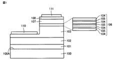
図1は、本発明の第1の実施形態の窒化物半導体発光素子の断面図である。本実施形態の窒化物半導体発光素子は、基板100と、基板100の上に設けられた下地層101と、下地層101の上に設けられた積層構造とを備える。基板100は、多結晶二酸化ケイ素またはアモルファス二酸化ケイ素を主成分として含む。下地層101は、c軸配向された結晶を含み、スパッタ法によって形成されたものである。または、下地層101は、c軸配向された結晶を含み、10原子%以下の希ガス原子を含む。積層構造は、窒化物半導体層(窒化物半導体単結晶からなる層)を少なくとも1つ有する。
<< First Embodiment >>
[Structure of nitride semiconductor light emitting device]
FIG. 1 is a cross-sectional view of a nitride semiconductor light emitting device according to a first embodiment of the present invention. The nitride semiconductor light emitting device of this embodiment includes a
本実施形態では、基板100の上には下地層101とバッファ層102と積層構造とが順に設けられており、積層構造ではn型窒化物半導体層103と発光層106とキャリアバリア層107とp型窒化物半導体層108とがバッファ層102の上に順に設けられている。n型窒化物半導体層103が露出するように積層構造がエッチングされており、n型窒化物半導体層103の露出面にはn側電極110が設けられている。また、p型窒化物半導体層108の上にはp側電極111が設けられている。
In the present embodiment, a
<基板>
(多結晶二酸化ケイ素またはアモルファス二酸化ケイ素)
基板100は、多結晶二酸化ケイ素またはアモルファス二酸化ケイ素を主成分として含む。そのため、基板100の製造コストを単結晶二酸化ケイ素基板の製造コストよりも低く抑えることができ、よって、基板100の製造コストを単結晶サファイア基板の製造コストよりも低く抑えることができる。したがって、本実施形態では、窒化物半導体層の成長用基板として単結晶サファイア基板を用いた場合に比べ、窒化物半導体層の成長用基板の製造コストを低減できるので、窒化物半導体発光素子の製造コストを低減できる。
<Board>
(Polycrystalline silicon dioxide or amorphous silicon dioxide)
The
本明細書では、「多結晶二酸化ケイ素またはアモルファス二酸化ケイ素を主成分として含む基板」とは、基板100が多結晶二酸化ケイ素またはアモルファス二酸化ケイ素を50質量%以上含むことを意味する。基板100は、好ましくは多結晶二酸化ケイ素またはアモルファス二酸化ケイ素を70質量%以上含み、より好ましくは多結晶二酸化ケイ素またはアモルファス二酸化ケイ素を90質量%以上含む。
In the present specification, the “substrate including polycrystalline silicon dioxide or amorphous silicon dioxide as a main component” means that the
本明細書では、ラマン分光法によって、基板100の材料が二酸化ケイ素であるか否かを確認している。また、FIB(Focused Ion Beam)装置で基板100を薄膜に加工して測定試料を作製し、作製された測定試料のTEM(Transmission Electron Microscope)画像またはSTEM(Scanning Transmission Electron Microscope)画像を観察することによって、基板100が多結晶二酸化ケイ素またはアモルファス二酸化ケイ素を含むか否かを確認している。上記TEM画像または上記STEM画像において、電子線回折像に弱いスポットが観察されれば多結晶二酸化ケイ素が基板100に含まれていると言え、電子線回折像の背景にハロー状のパターンが観察されればアモルファス二酸化ケイ素が基板100に含まれていると言える。
In this specification, whether or not the material of the
また、一般に、ラマンスペクトルには、分子構造の長距離秩序の程度が反映される。そのため、単結晶二酸化ケイ素と多結晶二酸化ケイ素とアモルファス二酸化ケイ素とでは、ラマンスペクトルの形状が明確に異なることとなる。よって、ラマンスペクトルの形状、ラマンスペクトルに現れる特定のピークのピーク強度、ラマンスペクトルに現れる特定のピークの半値幅、および、ラマンスペクトルに現れる特定のピークのピーク位置(ピーク波長)などを総合的に解析することによって、基板100における多結晶二酸化ケイ素またはアモルファス二酸化ケイ素の含有量を求めている。
In general, the Raman spectrum reflects the degree of long-range order of the molecular structure. Therefore, the shape of the Raman spectrum is clearly different between single crystal silicon dioxide, polycrystalline silicon dioxide, and amorphous silicon dioxide. Therefore, the shape of the Raman spectrum, the peak intensity of the specific peak appearing in the Raman spectrum, the half-width of the specific peak appearing in the Raman spectrum, the peak position (peak wavelength) of the specific peak appearing in the Raman spectrum, etc. By analyzing, the content of polycrystalline silicon dioxide or amorphous silicon dioxide in the
(第1原子)
基板100は、ケイ素(Si)原子および酸素(O)原子とは異なる第1原子をさらに含むことが好ましい。ここで、第1原子は、基板100に含有されることによって基板100の屈折率を二酸化ケイ素のみからなる基板の屈折率よりも大きくするものである。つまり、第1原子を基板100に添加することによって基板100の屈折率を高めることができる。よって、窒化物半導体発光素子からの光の取り出し効率をさらに高めることができる。ここで、「二酸化ケイ素のみからなる基板」とは、多結晶二酸化ケイ素またはアモルファス二酸化ケイ素からなる基板であって、Si原子およびO原子とは異なる原子をさらに含まない基板を意味する。
(First atom)
The
詳細には、窒化物半導体発光素子を構成する窒化物半導体としては、GaN、AlNまたはInNなどが知られている。これらの屈折率については、GaNの屈折率が2.54であり、AlNの屈折率が2.2であり、InNの屈折率が3.5である。これらの混晶の屈折率は、混晶の組成に応じて、混晶に含まれている窒化物半導体の屈折率の間の値を示すこととなる。そのため、何れの場合であっても、窒化物半導体と大気との屈折率差が1.2(=2.2−1)以上となるので、窒化物半導体発光素子からの光の取り出し効率を高めることは難しい。 Specifically, GaN, AlN, InN, or the like is known as a nitride semiconductor constituting the nitride semiconductor light emitting device. As for these refractive indexes, the refractive index of GaN is 2.54, the refractive index of AlN is 2.2, and the refractive index of InN is 3.5. The refractive index of these mixed crystals shows a value between the refractive indexes of the nitride semiconductors included in the mixed crystal according to the composition of the mixed crystal. Therefore, in any case, the refractive index difference between the nitride semiconductor and the atmosphere is 1.2 (= 2.2-1) or more, so that the light extraction efficiency from the nitride semiconductor light emitting device is increased. It ’s difficult.
しかし、二酸化ケイ素の屈折率は、1.5程度である。そのため、基板100を窒化物半導体層の成長用基板として用いれば、窒化物半導体層と基板100との屈折率差が0.7(=2.2−1.5)以上となり、基板100と大気との屈折率差が0.5(=1.5−1)程度となる。第1原子の添加によって、基板100の屈折率が大きくなるので、窒化物半導体層と基板100との屈折率差が小さくなる。これにより、下地層101側に位置する基板100の表面100A(以下では「下地層側に位置する基板の表面」を「基板の上面」と記す)においては、発光層106で生じた光の反射率を低く抑えることができる(スネルの法則)。よって、基板100がSi原子およびO原子だけでなく第1原子を含んでいれば、二酸化ケイ素のみからなる基板に比べ窒化物半導体発光素子からの光の取り出し効率を高めることができる。
However, the refractive index of silicon dioxide is about 1.5. Therefore, if the
好ましくは、第1原子は、ランタン(La)原子およびチタン(Ti)原子のうちの少なくとも1つであり、基板100に1×1010cm-3以上1×1012cm-3以下含まれる。例えば、基板100がSi原子およびO原子だけでなくLa原子を1×1010cm-3以上1×1012cm-3以下含んでいれば、かかる基板100の屈折率は二酸化ケイ素のみからなる基板の屈折率よりも約0.1〜0.15程度大きくなる。基板100がSi原子およびO原子だけでなくTi原子を1×1010cm-3以上1×1012cm-3以下含んでいれば、かかる基板100の屈折率は二酸化ケイ素のみからなる基板の屈折率よりも約0.03〜0.05程度大きくなる。
Preferably, the first atom is at least one of a lanthanum (La) atom and a titanium (Ti) atom, and is included in the
また、本発明者らは、基板100における第1原子の濃度が1×1012cm-3以下であれば発光層106で生じた光が第1原子に吸収される量を低く抑えることができるということを確認している。これにより、窒化物半導体発光素子からの光の取り出し量を確保できるので、窒化物半導体発光素子からの光の取り出し効率を高く維持できる。より好ましくは、基板100は第1原子を1×1010cm-3以上5×1011cm-3以下含む。
In addition, the present inventors can keep the amount of light generated in the
本明細書では、WD−TXRF(Wavelength-Dispersive Total reflection X-Ray Fluorescence)によって、基板100に含まれる第1原子の種類および濃度を求めている。基板100における第1原子の位置は特に限定されない。基板100が多結晶二酸化ケイ素を主成分として含む場合には、第1原子は、隣り合う単結晶二酸化ケイ素の間に設けられていても良いし、基板100において点在していても良い。基板100がアモルファス二酸化ケイ素を主成分として含む場合には、第1原子は、基板100において点在していることが好ましい。
In this specification, the type and concentration of the first atom contained in the
以上、基板100について説明したが、基板100は、多結晶二酸化ケイ素またはアモルファス二酸化ケイ素を主成分として含むので、可視光のみならず紫外線および深紫外線に対しても高い透過率を示す。「可視光」とは、波長が360nm以上830nm以下である電磁波を意味し、「紫外線」とは、波長が320nmよりも大きく360nm未満である電磁波を意味し、「深紫外線」とは、波長が200nm以上320nm以下である電磁波を意味する。そのため、基板100を用いて紫外線発光素子または深紫外線発光素子を提供することもできる。このことからも、単結晶サファイア基板の代替として基板100を使用できる。このような基板100の厚さは、200μm以上1500μm以下であることが好ましい。
Although the
<下地層>
上述したように、下地層101はスパッタ法で形成されたものである。そのため、基板100を窒化物半導体層の成長用基板として使用した場合であっても、下地層101の上には結晶品質に優れた窒化物半導体層を成長させることができる。このような効果が得られる理由としては次に示すことが考えられる。
<Underlayer>
As described above, the
スパッタ法では、不活性ガスのイオン化によって発生した電子またはイオンが高速でターゲットに衝突し、ターゲットを構成する重原子または分子がターゲットから叩き出される(スパッタリング現象)。スパッタリング現象によってイオン化された重原子または分子は、大きな運動エネルギーを持った状態で成膜面(本実施形態では基板100の上面100A)に到着し、その成膜面に付着する。このようにして、成膜面に膜が形成される。
In the sputtering method, electrons or ions generated by ionization of an inert gas collide with the target at high speed, and heavy atoms or molecules constituting the target are knocked out of the target (sputtering phenomenon). The heavy atoms or molecules ionized by the sputtering phenomenon arrive at the film formation surface (in this embodiment, the
このように、「スパッタ法」とは、成膜面において化学反応または相変化などを起こすことなくその成膜面に膜を物理的に形成する手法である。そのため、基板100の選択性がない。つまり、膜を化学的に形成する(例えばCVD(chemical vapor deposition)法などで膜を形成する)場合には使用できない基板を窒化物半導体層の成長用基板として使用できる。よって、基板100を窒化物半導体層の成長用基板として使用した場合であっても、基板100の結晶品質などを受け継ぐことなく下地層101を形成できる。
As described above, the “sputtering method” is a method of physically forming a film on the film formation surface without causing a chemical reaction or a phase change. Therefore, there is no selectivity of the
また、スパッタ法では、膜が成膜面に物理的に形成されるので、ターゲットの材料が本来有する性質が維持された状態で成膜可能である。それだけでなく、ターゲットの材料として高融点な材料を用いた場合であっても、ターゲットの材料の組成が維持された状態で成膜可能である。例えば、イオン性結合を有する材料は、c軸配向され易いという性質を有し、また、高い融点を有する。そのため、下地層101を形成するためのターゲットとしてイオン性結合を有する材料からなるターゲットを用いれば、c軸配向され易いという性質とターゲットの材料の組成とが維持された状態で下地層101を形成できる。よって、形成された下地層101は、c軸配向された結晶であってターゲットの材料の組成からなる結晶を含むこととなる。したがって、結晶品質に優れた下地層101を形成できる。それだけでなく、イオン性結合を有する材料からなるターゲットは低コストで入手されるので、下地層101を低コストで提供できる。また、スパッタ法では、膜が成膜面に物理的に形成されるので、化学反応の進行を考慮して成膜条件を設定または変更する必要がない。以上のことから、結晶品質に優れた下地層101を低コスト且つ容易に形成できる。
Further, in the sputtering method, the film is physically formed on the film formation surface, so that the film can be formed while maintaining the properties inherent to the target material. In addition, even when a material having a high melting point is used as the target material, film formation can be performed while the composition of the target material is maintained. For example, a material having an ionic bond has a property that it is easily c-axis oriented and has a high melting point. Therefore, if a target made of a material having an ionic bond is used as a target for forming the
さらに、スパッタ法では、イオン化された重原子または分子は、大きな運動エネルギーを持った状態で成膜面に到着するので、成膜面に対し強い付着力で付着する。よって、形成された下地層101の少なくとも一部が基板100の上面100Aから剥離することを防止できるので、貫通孔(例えばマイクロパイプ状の貫通孔)の形成を伴うことなく下地層101を形成できる。
Further, in the sputtering method, ionized heavy atoms or molecules arrive at the film formation surface with a large kinetic energy, and thus adhere to the film formation surface with a strong adhesion force. Therefore, since at least a part of the formed
以上より、基板100を窒化物半導体層の成長用基板として使用した場合であっても、イオン性結合を有する材料からなるターゲットを用いてスパッタ法で下地層101を基板100の上面100Aに形成すれば、貫通孔の形成を伴うことなく結晶品質に優れた下地層101を基板100の上面100Aに低コストで形成できる。これにより、基板100の上面100Aは、結晶品質に優れた下地層101によって被覆されることとなる。よって、下地層101の上には、基板100の結晶品質を継承することなく窒化物半導体層を形成できるので、結晶品質に優れた窒化物半導体層を形成できる。したがって、窒化物半導体層の成長用基板として単結晶サファイア基板を用いた場合に比べ、素子特性が現状維持または現状よりも高められた窒化物半導体発光素子を低コストで提供できる。
Thus, even when the
イオン性結合を有する材料としては、例えば、AlN、BNまたはGa2O3などが挙げられる。そのため、下地層101は、c軸配向された結晶として、c軸配向されたAlN結晶、c軸配向されたBN結晶およびc軸配向されたGa2O3結晶のうちの少なくとも1つを含むことが好ましい。下地層101のX線回折スペクトルを測定することによって、c軸配向された結晶の材料を確認できる。
Examples of the material having an ionic bond include AlN, BN, and Ga 2 O 3 . Therefore, the
より好ましくは、下地層101は、c軸配向された結晶とは別に、10原子%以下の酸素原子をさらに含む。これにより、下地層101に含まれる結晶(例えばAlN結晶、BN結晶またはGa2O3結晶など)のc軸配向性を高く維持できる。よって、窒化物半導体層の成長用基板として単結晶サファイア基板を用いた場合に比べ、素子特性がさらに高められた窒化物半導体発光素子を低コストで提供できる。さらに好ましくは、下地層101は、c軸配向された結晶とは別に、3原子%以上8原子%以下の酸素原子をさらに含む。本明細書では、「下地層は、c軸配向された結晶とは別に、10原子%以下の酸素原子をさらに含む」とは、かかる酸素原子がc軸配向された結晶の結晶構造を構成しないことを意味する。本明細書では、SIMS(Secondary Ion Mass Spectrometry)によって、下地層101における上記酸素原子の濃度を求めている。
More preferably, the
上述したように、イオン性結合を有する材料からなるターゲットを用いてスパッタ法で下地層101を形成することによって、c軸配向された結晶であってターゲットの材料の組成からなる結晶を含む下地層101を形成できる。そのため、本明細書では、「下地層は、c軸配向された結晶を含」むとは、下地層101が、イオン性結合を有する材料からなるターゲットを用いてスパッタ法によって形成されたことを意味する。
As described above, by forming the
また、「c軸配向された結晶」とは、結晶のc面((001)面)が基板100の上面100Aに対し平行となるように当該結晶が集積されていることを意味する。下地層101の面(0002)のX線ロッキングカーブの半値幅が1000秒以下であり、且つ、下地層101の面(1−102)のX線ロッキングカーブの半値幅が1000秒以下であれば、下地層101に含まれている結晶がc軸配向されていると言える。
The “c-axis oriented crystal” means that the crystal is integrated so that the c-plane ((001) plane) of the crystal is parallel to the
さらに、上述したように、スパッタ法では、不活性ガスの雰囲気下において成膜処理が行われるので、不活性ガスが取り込まれて成膜されると言われている。そのため、本明細書では、「下地層は、スパッタ法によって形成されたもの」は、「下地層は、10原子%以下の希ガス原子を含む」と言い換えることができ、好ましくは「下地層は、3原子%以上8原子%以下の希ガス原子を含む」と言い換えることができる。本明細書では、SIMSによって、下地層101における希ガス原子の濃度を求めている。なお、一般的には、不活性ガスとしては、アルゴン(Ar)、クリプトン(Kr)またはキセノン(Xe)などの希ガスが使用されている。
Furthermore, as described above, in the sputtering method, since the film forming process is performed in an atmosphere of an inert gas, it is said that the film is formed by taking in the inert gas. Therefore, in this specification, “the underlayer is formed by a sputtering method” can be rephrased as “the underlayer contains no more than 10 atomic% of noble gas atoms”. In other words, it includes 3 to 8 atomic% of noble gas atoms. In this specification, the concentration of rare gas atoms in the
以上、下地層101について説明したが、下地層101の厚さは500nm以上であることが好ましい。これにより、基板100の上面100Aが下地層101によって完全に被覆されることとなるので、下地層101の上に形成される窒化物半導体層の結晶品質をさらに高めることができる。より好ましくは、下地層101の厚さは500nm以上2000nm以下である。
The
<バッファ層>
バッファ層102が下地層101と積層構造との間に設けられていることによって、積層構造に含まれる窒化物半導体層の結晶品質をさらに高めることができる。これにより、窒化物半導体発光素子の素子特性をさらに向上させることができる。よって、窒化物半導体層の成長用基板として単結晶サファイア基板を用いた場合に比べ、素子特性がさらに高められた窒化物半導体発光素子を低コストで提供できる。
<Buffer layer>
By providing the
バッファ層102は、AlGaNからなっても良いが、AlNからなることが好ましい。バッファ層102がAlNからなれば、下地層101の材料と積層構造に含まれる窒化物半導体層の材料との格子不整合に起因するクラックの発生を防止できる。詳細には、積層構造に含まれる窒化物半導体層を構成する窒化物半導体の組成が考えられ得る組成のいずれであっても、バッファ層102が下地層101に対して圧縮応力を与えることとなる。よって、上記クラックの発生を防止できる。
The
このようなバッファ層102の厚さは2μm以上6μm以下であることが好ましい。これにより、積層構造に含まれる窒化物半導体層の結晶品質をさらに高めることができる。特に、バッファ層102の厚さが6μm以下であれば、バッファ層102が窒化物半導体層の結晶品質に対し悪影響を与えることを防止できる。
The thickness of the
<積層構造>
(n型窒化物半導体層)
n型窒化物半導体層103を構成する窒化物半導体は、GaN、AlGaN、InGaNまたはInAlGaNであることが好ましく、これらの少なくとも2つからなる混晶であっても良い。窒化物半導体発光素子に要求される発光波長に応じて、n型窒化物半導体層103を構成する窒化物半導体の組成が決定されることが好ましい。これにより、発光層106で生じた光がn型窒化物半導体層103で吸収されることを防止できる。よって、窒化物半導体発光素子からの光の取り出し量を確保できるので、窒化物半導体発光素子からの光の取り出し効率を高く維持できる。
<Laminated structure>
(N-type nitride semiconductor layer)
The nitride semiconductor constituting the n-type
例えば、n型窒化物半導体層103を構成する窒化物半導体がAlx1Ga1-x1N(0.7≦x1≦1)であれば、発光層106で生じた光(例えば深紫外線)がn型窒化物半導体層103で吸収されることを防止できる。また、n型窒化物半導体層103を構成する窒化物半導体がAlx2Ga1-x2N(0.5≦x2≦1)であれば、発光層106で生じた光(例えば紫外線)がn型窒化物半導体層103で吸収されることを防止できる。また、n型窒化物半導体層103を構成する窒化物半導体がInx3Ga1-x3N(0≦x3≦0.05)であれば、発光層106で生じた光(例えば可視光)がn型窒化物半導体層103で吸収されることを防止できる。
For example, if the nitride semiconductor constituting the n-type
n型窒化物半導体層103におけるn型不純物の濃度は、好ましくは1×1016cm-3以上8×1018cm-3以下であり、より好ましくは1×1016cm-3以上1×1018cm-3以下である。窒化物半導体発光素子に要求される素子特性に応じて、n型窒化物半導体層103におけるn型不純物の濃度が決定されることが好ましい。n型不純物は、Si、SeおよびGeのうちの少なくとも1つであれば良いが、Siであることが好ましい。
The concentration of the n-type impurity in the n-type
このようなn型窒化物半導体層103の厚さは、1μm以上4μm以下であることが好ましい。なお、n型窒化物半導体層103は、窒化物半導体の組成、n型不純物の濃度および厚さのうちの少なくとも1つが互いに異なる2以上の層が積層されて構成されたものであっても良い。
The thickness of the n-type
(発光層)
発光層106は、井戸層105が障壁層104で挟まれて構成されたものであることが好ましい。窒化物半導体発光素子に要求される発光波長または素子特性などに応じて、障壁層104を構成する窒化物半導体の組成、障壁層104の厚さ、井戸層105を構成する窒化物半導体の組成、または、井戸層105の厚さが決定されることが好ましい。また、障壁層104の厚さ、および、井戸層105の厚さに関しては、発光層106での量子準位の形成をさらに考慮して決定されることが好ましい。
(Light emitting layer)
The
例えば、深紫外線を発生させる窒化物半導体発光素子では、井戸層105は、好ましくはAlを含み、より好ましくはAls1Ga1-s1N(0.4≦s1≦0.6)からなる。また、紫外線を発生させる窒化物半導体発光素子では、井戸層105は、好ましくはAlを含み、より好ましくはAls2Ga1-s2N(0.05≦s2≦0.3)からなる。また、可視光を発生させる窒化物半導体発光素子では、井戸層105は、好ましくはInを含み、より好ましくはIns3Ga1-s3N(0.08≦s3≦0.7)からなる。
For example, in a nitride semiconductor light emitting device that generates deep ultraviolet rays, the
また、障壁層104は、井戸層105よりも大きなバンドギャップエネルギーを有することが好ましく、発光層106で生じた光を吸収しないことが好ましい。例えば、深紫外線を発生させる窒化物半導体発光素子では、障壁層104を構成する窒化物半導体のAl組成は井戸層105を構成する窒化物半導体のAl組成よりも高いことが好ましい。例えば、障壁層104は、Alt1Ga1-t1N(0.45≦t1≦0.65)からなることが好ましい。このように、深紫外線を発生させる窒化物半導体発光素子では、障壁層104および井戸層105のそれぞれを構成する窒化物半導体のAl組成が高くなるので、正孔(正孔は有効質量が大きい)がp型窒化物半導体層108から発光層106(特に井戸層105)に注入され難くなる。そのため、障壁層104の厚さを大きくすると、正孔が井戸層105に注入され難くなる。また、井戸層105の厚さを大きくすると、発光層106の厚さ方向中央に位置する井戸層105に対する正孔の注入が困難となる。以上のことから、障壁層104の厚さは、好ましくは5nm以下であり、より好ましくは1nm以上5nm以下である。また、井戸層105の厚さは、好ましくは5nm以下であり、より好ましくは1nm以上5nm以下である。
The
また、紫外線を発生させる窒化物半導体発光素子では、障壁層104を構成する窒化物半導体のAl組成は井戸層105を構成する窒化物半導体のAl組成よりも高いことが好ましい。例えば、障壁層104は、Alt2Ga1-t2N(0.08≦t2≦0.35)からなることが好ましい。この場合、障壁層104の厚さは、好ましくは5nm以下であり、より好ましくは1nm以上5nm以下である。また、井戸層105の厚さは、好ましくは5nm以下であり、より好ましくは1nm以上5nm以下である。
In the nitride semiconductor light emitting device that generates ultraviolet light, the Al composition of the nitride semiconductor constituting the
また、可視光を発生させる窒化物半導体発光素子では、障壁層104を構成する窒化物半導体のIn組成は井戸層105を構成する窒化物半導体のIn組成よりも低いことが好ましい。例えば、障壁層104は、Int3Ga1-t3N(0.05≦t3≦0.65)からなることが好ましい。この場合、障壁層104の厚さは、好ましくは5nm以下であり、より好ましくは1nm以上5nm以下である。また、井戸層105の厚さは、好ましくは5nm以下であり、より好ましくは1nm以上5nm以下である。
In the nitride semiconductor light emitting element that generates visible light, the In composition of the nitride semiconductor that forms the
p型窒化物半導体層108から発光層106(特に井戸層105)への正孔の注入効率を高く維持できるのであれば、発光層106における障壁層104の層数は限定されず、発光層106における井戸層105の層数もまた限定されない。
The number of barrier layers 104 in the light-emitting
(キャリアバリア層)
キャリアバリア層107とは、発光層106に注入された電子がp型窒化物半導体層108側へオーバーフローすることを防止する機能を有する層を意味する。そのため、キャリアバリア層107を構成する窒化物半導体のAl組成は、障壁層104および井戸層105のそれぞれを構成する窒化物半導体のAl組成よりも高いことが好ましい。また、キャリアバリア層107は、上記機能を発揮できる厚さの最小値以上の厚さを有することが好ましい。
(Carrier barrier layer)
The
一方、窒化物半導体のAl組成が高い層の厚さを大きくすると、窒化物半導体発光素子の直列抵抗の増大を招き、よって、窒化物半導体発光素子の電力変換効率の低下を引き起こす。それだけでなく、キャリアバリア層107の厚さが大きければ、正孔がp型窒化物半導体層108から発光層106(特に井戸層105)に注入され難くなる。以上をふまえて、キャリアバリア層107を構成する窒化物半導体の組成とキャリアバリア層107の厚さとを決定することが好ましい。例えば、キャリアバリア層107は、好ましくはAlu1Ga1-u1N(0.7≦u1≦0.9)からなり、より好ましくはAlu1Ga1-u1N(0.75≦u1≦0.9)からなる。また、キャリアバリア層107の厚さは、好ましくは10nm以上200nm以下であり、より好ましくは30nm以上200nm以下である。
On the other hand, when the thickness of the layer having a high Al composition in the nitride semiconductor is increased, the series resistance of the nitride semiconductor light emitting device is increased, and thus the power conversion efficiency of the nitride semiconductor light emitting device is lowered. In addition, if the thickness of the
なお、キャリアバリア層107はp型不純物を含むことが好ましい。これにより、窒化物半導体発光素子の直列抵抗を低く抑えることができる。p型不純物としてはMgを使用できる。
Note that the
(p型窒化物半導体層)
p型窒化物半導体層108を構成する窒化物半導体については、n型窒化物半導体層103を構成する窒化物半導体と同様のことが言える。例えば、p型窒化物半導体層108を構成する窒化物半導体がAly1Ga1-y1N(0.7≦y1≦1)であれば、発光層106で生じた光(例えば深紫外線)がp型窒化物半導体層108で吸収されることを防止できる。また、p型窒化物半導体層108を構成する窒化物半導体がAly2Ga1-y2N(0.5≦y2≦1)であれば、発光層106で生じた光(例えば紫外線)がp型窒化物半導体層108で吸収されることを防止できる。また、p型窒化物半導体層108を構成する窒化物半導体がIny3Ga1-y3N(0≦y3≦0.05)であれば、発光層106で生じた光(例えば可視光)がp型窒化物半導体層108で吸収されることを防止できる。
(P-type nitride semiconductor layer)
The same applies to the nitride semiconductor constituting the p-type
p型窒化物半導体層108におけるp型不純物の濃度は1×1018cm-3以上1×1020cm-3以下であることが好ましい。窒化物半導体発光素子に要求される素子特性に応じて、p型窒化物半導体層108におけるp型不純物の濃度が決定されることが好ましい。例えば、p型窒化物半導体層108におけるp型不純物の濃度が高ければ、窒化物半導体発光素子の直列抵抗を低く抑えることができる。
The concentration of the p-type impurity in the p-type
このようなp型窒化物半導体層108の厚さは、好ましくは0.05μm以上1.5μm以下であり、より好ましくは0.5μm以上1.5μm以下である。なお、p型窒化物半導体層108は、キャリアバリア層107の上に設けられた第1p型窒化物半導体層と、第1p型窒化物半導体層の上に設けられ、且つ、p型不純物の濃度が第1p型窒化物半導体層よりも高い第2p型窒化物半導体層とを有することが好ましい。これにより、窒化物半導体発光素子の直列抵抗をさらに低く抑えることができる。
The thickness of such p-type
<n側電極、p側電極>
n側電極110の材料としては、n型窒化物半導体層に対するコンタクト電極の材料として一般的な材料を特に限定されることなく使用でき、例えば、Ni/Auを使用できる。p側電極111の材料としては、p型窒化物半導体層に対するコンタクト電極の材料として一般的な材料を特に限定されることなく使用でき、例えば、Pd/Auを使用できる。
<N-side electrode, p-side electrode>
As a material of the n-
n側電極110の厚さは、n型窒化物半導体層に対するコンタクト電極の厚さとして一般的な厚さを特に限定されることなく採用できるが、1μm以上であることが好ましい。これにより、n側電極110に対してワイヤーボンディングを行うことができる。p側電極111の厚さについても同様のことが言える。
As the thickness of the n-
[窒化物半導体発光素子の製造]
以下に示す窒化物半導体発光素子の製造方法では、窒化物半導体発光素子形成用ウエハ(以下では単に「ウエハ」と記す)をチップに分割することによって本実施形態の窒化物半導体発光素子を得ている。以下では、ウエハの構成要素には窒化物半導体発光素子の対応する構成要素の符号を付して、窒化物半導体発光素子の製造方法を説明する。なお、ウエハの構成要素の材料および厚さなどについては、上記[窒化物半導体発光素子の構造]で説明した通りである。
[Manufacture of nitride semiconductor light emitting devices]
In the nitride semiconductor light emitting device manufacturing method shown below, the nitride semiconductor light emitting device of this embodiment is obtained by dividing a nitride semiconductor light emitting device forming wafer (hereinafter simply referred to as “wafer”) into chips. Yes. In the following description, a method for manufacturing a nitride semiconductor light-emitting device will be described by attaching the reference numerals of the corresponding components of the nitride semiconductor light-emitting device to the components of the wafer. The material and thickness of the constituent elements of the wafer are as described in the above [Structure of nitride semiconductor light emitting device].
<下地層の形成>
下地層101の形成工程では、基板100の上に、c軸配向された結晶を含む下地層101をスパッタ法によって形成する。
<Formation of underlayer>
In the formation process of the
例えば、まず、基板100をスパッタ装置内の所定の位置に設置し、また、ターゲットをスパッタ装置内の所定の位置に設置する。このとき、基板100の上面100Aがターゲットに対向するように、基板100をスパッタ装置内に設置する。
For example, first, the
スパッタ装置内に設置される基板100としては、直径が2インチ(50.8mm)以上の基板100を使用することが好ましく、直径が4インチ(101.6mm)以上の基板100を使用することがより好ましい。直径が4インチ以上の基板100の方が、直径が2インチ以上の基板100に比べ、単位面積当たりの価格を低く抑えることができる。よって、直径が4インチ(101.6mm)以上の基板100を使用すれば、窒化物半導体発光素子の製造コストをさらに低く抑えることができる。
As the
また、スパッタ装置内に設置される基板100としては、有機溶媒により洗浄された後に純水により洗浄された基板100を使用することが好ましい。この2回にわたる洗浄によって、基板100の表面から有機物または微粒子状付着物などを除去することができる。よって、有機物または微粒子状付着物などが表面に付着していない基板100を窒化物半導体層の成長用基板として用いることができる。ここで、有機溶媒としては、洗浄用溶媒として一般的に使用されている有機溶媒を使用できる。
As the
スパッタ装置内に設置されるターゲットとしては、単結晶材料からなるターゲットを使用しても良いが、多結晶材料からなるターゲットを使用することが好ましい。これにより、下地層101の形成コストを低く抑えることができるので、窒化物半導体発光素子の製造コストを低く抑えることができる。
As a target installed in the sputtering apparatus, a target made of a single crystal material may be used, but a target made of a polycrystalline material is preferably used. Thereby, since the formation cost of the foundation |
スパッタ装置としては、窒化物半導体発光素子を製造するために一般的に使用されているスパッタ装置を特に限定されることなく使用できる。 As the sputtering apparatus, a sputtering apparatus generally used for manufacturing a nitride semiconductor light emitting element can be used without any particular limitation.
次に、スパッタ装置内を真空引きした後、不活性ガスをスパッタ装置内に導入し、基板100とターゲットとの間に高周波電圧を印加する。これにより、スパッタ装置内では、高周波放電が起こるので、スパッタリング現象が発生する。よって、下地層101がスパッタ法によって基板100の上面100Aに形成されることとなる。
Next, after evacuating the sputtering apparatus, an inert gas is introduced into the sputtering apparatus, and a high-frequency voltage is applied between the
下地層101の形成時には、基板100を加熱しなくても良いが、基板100を加熱する方が好ましい。下地層101の形成時における基板100の加熱によって、下地層101に含まれる結晶がc軸配向され易くなるので、結晶品質に優れた下地層101が形成され易くなる。このような効果を効果的に得るためには、基板100の加熱温度を400℃以下とすることが好ましく、基板100の加熱温度を50℃以上150℃以下とすることがより好ましい。基板100の加熱温度が400℃以下であれば、ターゲットの材料が窒素原子を含む場合(例えばターゲットがAlNからなる場合)において窒素原子がターゲットから解離することを防止できるという効果も得られる。
When the
<バッファ層の形成>
バッファ層102の形成工程では、下地層101の上にバッファ層102を例えばMOCVD(Metal Organic Chemical Vapor Deposition)法によって形成する。これにより、バッファ層102の量産に資するので、窒化物半導体発光素子の量産に資する。
<Formation of buffer layer>
In the formation process of the
例えば、まず、下地層101が形成された基板100をスパッタ装置から取り出しMOCVD装置内に設置する。MOCVD装置としては、窒化物半導体発光素子を製造するために一般的に使用されているMOCVD装置を特に限定されることなく使用できる。
For example, first, the
次に、基板100の温度を上昇させる。このとき、水素、アンモニアおよび窒素のうちの少なくとも1つを含む雰囲気下で基板100の温度を上昇させることが好ましい。下地層101が窒素原子を含む場合(例えば下地層101がc軸配向されたAlN結晶を含む場合)には、アンモニアを含む雰囲気下で基板100の温度上昇させることが好ましい。これにより、基板100の温度が400℃を超えても、下地層101からの窒素原子の解離を防止できる。
Next, the temperature of the
続いて、基板100の温度を保持した状態で、窒化物半導体単結晶の成長を開始する。深紫外線を発生させる窒化物半導体発光素子を製造する場合には、Alを含む窒化物半導体単結晶を成長させる場合が多い。そのため、基板100の温度を1000℃以上の温度に保持した状態で窒化物半導体単結晶を成長させることが好ましい。紫外線を発生させる窒化物半導体発光素子を製造する場合には、Alを含む窒化物半導体単結晶を成長させる場合が多い。そのため、基板100の温度を1200℃以上の温度に保持した状態で窒化物半導体単結晶を成長させることが好ましい。可視光を発生させる窒化物半導体発光素子を製造する場合には、Inを含む窒化物半導体単結晶を成長させる場合が多い。そのため、基板100の温度を700℃以下の温度に保持した状態で窒化物半導体単結晶を成長させることが好ましい。
Subsequently, the growth of the nitride semiconductor single crystal is started while the temperature of the
<積層構造の形成>
積層構造の形成工程では、バッファ層102の上に、n型窒化物半導体層103、発光層106、キャリアバリア層107およびp型窒化物半導体層108を順に形成する。MOCVD法によって積層構造を形成することが好ましい。このとき、バッファ層102を形成するために使用したMOCVD装置を用いて積層構造を形成しても良いし、バッファ層102を形成するために使用したMOCVD装置とは異なるMOCVD装置を用いて積層構造を形成しても良い。このようにしてウエハが作製される。
<Formation of laminated structure>
In the formation process of the stacked structure, the n-type
<n側電極およびp側電極の形成>
n側電極110およびp側電極111の形成工程では、n型窒化物半導体層103の露出面にn側電極110を形成し、p型窒化物半導体層108の上面にp側電極111を形成する。
<Formation of n-side electrode and p-side electrode>
In the formation process of the n-
例えば、まず、ウエハをMOCVD装置から取り出した後、p型不純物の活性化を行う。その後、フォトリソグラフィとRIE(Reactive Ion Etching)とによってp型窒化物半導体層108、キャリアバリア層107、発光層106およびn型窒化物半導体層103をエッチングし、n型窒化物半導体層103の露出面を形成する。例えば真空蒸着法によって、n型窒化物半導体層103の露出面にn側電極110を形成する。
For example, first, after removing the wafer from the MOCVD apparatus, p-type impurities are activated. Thereafter, the p-type
また、例えばフォトリソグラフィによって、p型窒化物半導体層108の上面のうちp側電極111の形成領域とは異なる領域にマスクを形成する。その後、例えば真空蒸着法によって、p型窒化物半導体層108の上面のうち上記マスクから露出する部分にp側電極111を形成する。
Further, a mask is formed in a region different from the formation region of the p-
n側電極110およびp側電極111の形成後に熱処理を行うことが好ましい。これにより、n側電極110が焼結化され、よって、n側電極110とn型窒化物半導体層103とがオーミックコンタクトされる。また、p側電極111が焼結化され、よって、p側電極111とp型窒化物半導体層108とがオーミックコンタクトされる。
Heat treatment is preferably performed after the n-
<個片化>
例えばダイシングまたはレーザスクライブなどによってウエハをチップに分割する。このようにして窒化物半導体発光素子が製造される。好ましくは、製造された窒化物半導体発光素子をステムに実装し、窒化物半導体発光素子とステムとを電気的に接続した後、樹脂などによって窒化物半導体発光素子を封止する。
<Individualization>
For example, the wafer is divided into chips by dicing or laser scribing. In this way, a nitride semiconductor light emitting device is manufactured. Preferably, the manufactured nitride semiconductor light emitting element is mounted on a stem, and after the nitride semiconductor light emitting element and the stem are electrically connected, the nitride semiconductor light emitting element is sealed with a resin or the like.
≪第2の実施形態≫
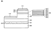
図2は、本発明の第2の実施形態の窒化物半導体発光素子の断面図である。本実施形態の窒化物半導体発光素子は、上記第1の実施形態の基板100の代わりに、上面に凹凸210が形成された基板200を備えている。以下では、上記第1の実施形態とは異なる点を主に説明する。
<< Second Embodiment >>
FIG. 2 is a cross-sectional view of the nitride semiconductor light emitting device according to the second embodiment of the present invention. The nitride semiconductor light emitting device of this embodiment includes a
本実施形態では、基板200の上面に凹凸210が形成されているので、基板200の上面では発光層106で生じた光が散乱することとなる。これにより、凹凸210の表面に対して所定の入射角(0°<入射角<90°)で入射した光(発光層106で生じた光)も窒化物半導体発光素子の外へ取り出されることとなるので、窒化物半導体発光素子からの光の取り出し効率をさらに高めることができる。
In this embodiment, since the
下地層101を基板200の上面に化学的に形成する場合には、基板200の上面では化学反応の進行または反応性ガスの流れなどが凹凸210によって不均一となる。そのため、基板200の上面において成膜処理を均一に行うことが難しく、成膜処理は基板200の上面の平坦性などの影響を受けることとなる。
When the
しかし、本実施形態では、上記第1の実施形態と同じく、下地層101は、基板200の上面にスパッタ法によって形成されたものであるので、基板200の上面に物理的に形成されたものである。そのため、化学反応の進行または反応性ガスの流れなどの影響を受けることなく下地層101を形成できる。よって、基板200の上面に凹凸210が形成されている場合であっても、基板200の上面には結晶品質が均一な下地層101を形成することができるので、下地層101の上には結晶品質が均一な窒化物半導体層を形成できる。したがって、基板200の上面に凹凸210を形成することによって窒化物半導体発光素子の光の取り出し効率の向上を実現できる。以上より、窒化物半導体層の成長用基板として単結晶サファイア基板を用いた場合に比べ、素子特性(例えば光の取り出し効率)がさらに高められた窒化物半導体発光素子を低コストで提供できる。
However, in the present embodiment, as in the first embodiment, since the
凹凸210では、凹部または凸部の形状、凹部または凸部の大きさ、凹部または凸部の個数、または、凹部または凸部の間隔などは特に限定されない。また、隣り合う凹部においては、凹部の形状または大きさは互いに同じであっても互いに異なっても良い。このことは隣り合う凸部についても言える。さらに、基板200の上面において凹部の間隔は均一であっても互いに異なっても良い。このことは基板200の上面における凸部の間隔についても言える。例えば、凹部または凸部の形状は円錐または多角錐であることが好ましく、凹部の深さまたは凸部の高さは50nm以上500nm以下であることが好ましく、隣り合う凹部の間隔または隣り合う凸部の間隔は50μm以上200μm以下であることが好ましい。
In the
凹凸210の形成方法は特に限定されない。単結晶サファイア基板に対して凹凸加工を行う場合には、高出力エキシマレーザ光などを単結晶サファイア基板に照射する必要がある。そのため、単結晶サファイア基板に対する凹凸加工には困難を伴う。しかし、基板200は多結晶二酸化ケイ素またはアモルファス二酸化ケイ素を主成分として含んでいるので、サンドブラスト、または、フッ化水素酸を含むエッチャントを用いたウエットエッチングによって、基板200に対して凹凸加工を行うことができる。よって、単結晶サファイア基板に対する凹凸加工よりも基板200に対する凹凸加工を容易に且つ低コストで行うことができる。したがって、窒化物半導体層の成長用基板として単結晶サファイア基板を用いた場合に比べ、素子特性(例えば光の取り出し効率)がさらに高められた窒化物半導体発光素子をさらに低コストで提供できる。
The formation method of the unevenness |
サンドブラストの条件としては、基板の表面に凹凸を形成するときのサンドブラストの条件として一般的な条件を特に限定されることなく使用できる。サンドブラストで使用される研磨剤粒子の大きさ、または、研磨剤粒子を基板200の上面に噴射する時間などを変更すれば、凹凸210の形状または大きさが変更される。
As conditions for sandblasting, general conditions can be used without particular limitation as conditions for sandblasting when forming irregularities on the surface of the substrate. If the size of the abrasive particles used in sandblasting or the time during which the abrasive particles are sprayed onto the upper surface of the
また、フッ化水素酸を含むエッチャントを用いたウエットエッチングの条件としては、基板の表面に凹凸を形成するときのウエットエッチングの条件として一般的な条件を特に限定されることなく使用できる。基板200の上面を上記エッチャントに浸漬させる時間などを変更すれば、凹凸210の形状または大きさが変更される。
Moreover, as conditions for wet etching using an etchant containing hydrofluoric acid, general conditions can be used without particular limitation as conditions for wet etching when forming irregularities on the surface of the substrate. If the time for immersing the upper surface of the
≪第3の実施形態≫
図3は、本発明の第3の実施形態の窒化物半導体発光素子の製造工程の一工程を示す断面図である。図4は、本実施形態の窒化物半導体発光素子の断面図である。本実施形態では、積層構造を形成した後に基板100を除去する。そのため、製造された窒化物半導体発光素子は基板100を備えていない(図4)。以下では、上記第1の実施形態とは異なる点を主に説明する。
<< Third Embodiment >>
FIG. 3 is a cross-sectional view showing one step of the manufacturing process of the nitride semiconductor light emitting device of the third embodiment of the present invention. FIG. 4 is a cross-sectional view of the nitride semiconductor light emitting device of this embodiment. In this embodiment, the
[窒化物半導体発光素子の製造]
<積層構造およびp側電極の形成>
まず、上記第1の実施形態に記載の方法にしたがってウエハを形成した後、p型不純物を活性化させる。積層構造などをエッチングすることなく、上記第1の実施形態に記載の方法にしたがってp型窒化物半導体層108の上面にp側電極311を形成する。その後、p側電極311の上面に支持基体312を接着する。このようにして図3に示す積層体が形成される。
[Manufacture of nitride semiconductor light emitting devices]
<Formation of laminated structure and p-side electrode>
First, after forming a wafer according to the method described in the first embodiment, the p-type impurity is activated. The p-
支持基体312は、導電性を有することが好ましい。これにより、窒化物半導体発光素子への電圧印加時に発生する電気抵抗を低く抑えることができる。
The
より好ましくは、支持基体312は、積層構造に含まれる窒化物半導体層を構成する窒化物半導体と同程度の熱膨張係数を有する材料からなる。これにより、支持基体312の材料と積層構造に含まれる窒化物半導体層の材料との熱膨張係数差に起因するクラックの発生を防止できる。このような材料としては、例えば、タングステンが挙げられる。
More preferably, the
支持基体312をp側電極311の上面に接着させるための接着剤は導電性を有することが好ましい。これによっても、窒化物半導体発光素子への電圧印加時に発生する電気抵抗を低く抑えることができる。このような接着剤は、集積回路(Integrated Circuit)を実装基板などに接着させるときに一般的に使用される接着剤(例えば熱硬化性を有する接着剤)であることが好ましいが、低融点な接着剤(例えばハンダ)であっても良い。
The adhesive for bonding the
<基板の除去>
次に、図3に示す積層体をフッ化水素酸を含むエッチャントに浸漬させる。これにより、基板100が選択的に除去される。基板100の大きさに応じて、図3に示す積層体を上記エッチャントへ浸漬させる時間を変更することが好ましい。
<Removal of substrate>
Next, the laminate shown in FIG. 3 is immersed in an etchant containing hydrofluoric acid. Thereby, the
<n側電極の形成>
続いて、基板100が除去されることにより露出した下地層101の表面(「積層構造とは反対側に位置する下地層101の表面」とも言える。以下では、「下地層の露出面」と記す)101Aにn側電極310を形成する。このとき、n側電極310を下地層101の露出面101Aにストライプ状に形成することが好ましく、より好ましくはn側電極310を下地層101の露出面101Aにマトリックス状に形成する。このようにして、本実施形態の窒化物半導体発光素子が製造される(図4)。
<Formation of n-side electrode>
Subsequently, the surface of the
[窒化物半導体発光素子の構成]
このようにして製造された窒化物半導体発光素子では、図4に示すように、下地層101とバッファ層102とn型窒化物半導体層103と発光層106とキャリアバリア層107とp型窒化物半導体層108とがこの順に設けられている。n側電極310は、下地層101の露出面101Aにおいてストライプ状またはマトリックス状に設けられており、p側電極311は、p型窒化物半導体層108の下面に設けられている。
[Configuration of nitride semiconductor light emitting device]
In the nitride semiconductor light emitting device manufactured in this way, as shown in FIG. 4, the
本実施形態の窒化物半導体発光素子では、n側電極310は素子の上面側に設けられており、p側電極311は素子の下面側に設けられている。これにより、本実施形態の窒化物半導体発光素子では、n側電極310とp側電極311との間を流れる電流は、発光層106に対し垂直に流れることとなる。つまり、本実施形態の窒化物半導体発光素子は、いわゆる縦型構造の窒化物半導体発光素子である。
In the nitride semiconductor light emitting device of this embodiment, the n-
ここで、窒化物半導体発光素子には、縦型構造の窒化物半導体発光素子と横型構造の窒化物半導体発光素子とが存在する。横型構造の窒化物半導体発光素子では、n側電極とp側電極との間を流れる電流が発光層に対し平行に流れる(図1または図2参照)。そのため、横型構造の窒化物半導体発光素子では、縦型構造の窒化物半導体発光素子に比べ、発光層106での発光面積が小さくなるので、窒化物半導体発光素子の単位サイズ当たりの光の取り出し量が低下する。また、電流が窒化物半導体発光素子の内部を流れるときに発生する電気抵抗が増加する。よって、縦型構造の窒化物半導体発光素子と横型構造の窒化物半導体発光素子とにおいて素子構造が全く同一であれば、縦型構造の窒化物半導体発光素子の方が横型構造の窒化物半導体発光素子よりも優れた素子特性を示すこととなる。以上のことから、横型構造の窒化物半導体発光素子よりも縦型構造の窒化物半導体発光素子を提供することが好ましいと言われている。
Here, the nitride semiconductor light emitting device includes a vertical structure nitride semiconductor light emitting device and a lateral structure nitride semiconductor light emitting device. In the nitride semiconductor light emitting device having a lateral structure, a current flowing between the n-side electrode and the p-side electrode flows in parallel to the light emitting layer (see FIG. 1 or FIG. 2). Therefore, in the nitride semiconductor light emitting device having the lateral structure, the light emission area in the
しかし、縦型構造の窒化物半導体発光素子を製造するためには、その製造過程において窒化物半導体層の成長用基板を除去する必要がある。窒化物半導体層の成長用基板として単結晶サファイア基板を用いた場合には、高出力エキシマレーザ光などを単結晶サファイア基板に照射することによって単結晶サファイア基板を除去することとなる。そのため、窒化物半導体層の成長用基板の除去に困難を伴うため、縦型構造の窒化物半導体発光素子を低コストで提供することが難しくなる。 However, in order to manufacture a nitride semiconductor light emitting device having a vertical structure, it is necessary to remove the growth substrate of the nitride semiconductor layer in the manufacturing process. When a single crystal sapphire substrate is used as the growth substrate for the nitride semiconductor layer, the single crystal sapphire substrate is removed by irradiating the single crystal sapphire substrate with a high-power excimer laser beam or the like. Therefore, it is difficult to remove the growth substrate for the nitride semiconductor layer, so that it is difficult to provide a nitride semiconductor light emitting element having a vertical structure at low cost.
一方、窒化物半導体層の成長用基板として基板100を用いた場合には、図3に示す積層体を上記エッチャントに浸漬させることによって基板100を除去することができる。なぜならば、基板100の主成分である多結晶二酸化ケイ素またはアモルファス二酸化ケイ素がフッ化水素酸によって溶解されるためである。よって、困難を伴うことなく基板100を除去できるので、縦型構造の窒化物半導体発光素子を容易に且つ低コストで提供できる。以上より、本実施形態では、窒化物半導体層の成長用基板として単結晶サファイア基板を用いた場合に比べ、素子特性(例えば光の取り出し効率)がさらに高められた窒化物半導体発光素子をさらに低コストで提供できることとなる。
On the other hand, when the
それだけでなく、p側電極311は、上記第1の実施形態で説明したように金属からなるので、発光層106で生じた光をn側電極310側へ反射させるための反射層として機能し得る。これにより、発光層106で生じた光の多くは、n側電極310側から窒化物半導体発光素子の外側へ取り出されることとなる。そのため、n側電極310が下地層101の露出面101Aにおいてストライプ状に設けられていれば、発光層106で生じた光は、下地層101の露出面101Aのうちn側電極310が設けられていない部分から優先的に窒化物半導体発光素子の外へ取り出されることとなる。よって、n側電極310が下地層101の露出面101A全体に設けられている場合に比べ、光(発光層106で生じた光)がn側電極310によって遮られる量を少なく抑えることができる。したがって、本実施形態においてn側電極310が下地層101の露出面101Aにおいてストライプ状に設けられていれば、窒化物半導体層の成長用基板として単結晶サファイア基板を用いた場合に比べ素子特性(例えば光の取り出し効率)がより一層高められた窒化物半導体発光素子をさらに低コストで提供できる。
In addition, since the p-
n側電極310が下地層101の露出面101Aにおいてマトリックス状に設けられていれば、光(発光層106で生じた光)がn側電極310によって遮られる量をさらに少なく抑えることができる。よって、本実施形態においてn側電極310が下地層101の露出面101Aにおいてマトリックス状に設けられていれば、窒化物半導体層の成長用基板として単結晶サファイア基板を用いた場合に比べ素子特性(例えば光の取り出し効率)がさらに一層高められた窒化物半導体発光素子をさらに低コストで提供できる。
If the n-
n側電極310の大きさまたは形状、または、隣り合うn側電極310の間隔などは特に限定されない。例えば、下地層101の露出面101Aの露出割合(=下地層101の露出面101Aのうちn側電極310に被覆されていない部分の面積÷下地層101の露出面101Aの面積)が5%以上20%以下となるように、n側電極310が下地層101の露出面101Aに設けられていることが好ましい。
There is no particular limitation on the size or shape of the n-
なお、基板100を除去するタイミングは本実施形態で示すタイミングに限定されない。積層構造を構成する窒化物半導体層が1層以上形成された後に基板100を除去することが好ましい。
Note that the timing of removing the
また、本実施形態では、窒化物半導体層の成長用基板として基板100ではなく基板200を使用しても良い。しかし、基板100の上面の方が基板200の上面よりも平坦である。そのため、窒化物半導体層の成長用基板として基板100を使用した方が、基板100を容易に除去でき、また、外観に優れた窒化物半導体発光素子を製造できる。さらには、窒化物半導体発光素子の製造時または使用時における下地層101の欠けなどを防止できる。
In this embodiment, the
[実施形態の総括]
図1または図2に示す窒化物半導体発光素子は、多結晶二酸化ケイ素またはアモルファス二酸化ケイ素を主成分として含む基板100,200と、基板100,200の上に設けられた下地層101と、下地層101の上に設けられ、窒化物半導体単結晶からなる層を少なくとも1つ有する積層構造とを備える。下地層101は、c軸配向された結晶を含み、スパッタ法によって形成されたものである。これにより、窒化物半導体層の成長用基板として単結晶サファイア基板を用いた場合に比べ、素子特性が現状維持または現状よりも高められた窒化物半導体発光素子を低コストで提供できる。
[Summary of Embodiment]
The nitride semiconductor light emitting device shown in FIG. 1 or FIG. 2 includes
図1または図2に示す窒化物半導体発光素子は、多結晶二酸化ケイ素またはアモルファス二酸化ケイ素を主成分として含む基板100,200と、基板100,200の上に設けられた下地層101と、下地層101の上に設けられ、窒化物半導体単結晶からなる層を少なくとも1つ有する積層構造とを備える。下地層101は、c軸配向された結晶を含み、10原子%以下の希ガス原子を含む。これによっても、窒化物半導体層の成長用基板として単結晶サファイア基板を用いた場合に比べ、素子特性が現状維持または現状よりも高められた窒化物半導体発光素子を低コストで提供できる。
The nitride semiconductor light emitting device shown in FIG. 1 or FIG. 2 includes
下地層101は、c軸配向された結晶として、c軸配向されたAlN結晶、c軸配向されたBN結晶およびc軸配向されたGa2O3結晶うちの少なくとも1つを含むことが好ましい。
The
下地層101は、c軸配向された結晶とは別に、10原子%以下の酸素原子をさらに含むことが好ましい。これにより、下地層101に含まれる結晶のc軸配向性を高めることができる。
The
下地層101側に位置する基板200の表面には凹凸210が形成されていることが好ましい。これにより、窒化物半導体発光素子の光の取り出し効率を高めることができる。
基板100,200は、ケイ素原子および酸素原子とは異なる第1原子をさらに含むことが好ましい。第1原子は、基板100,200に含有されることによって基板100,200の屈折率を二酸化ケイ素のみからなる基板の屈折率よりも大きくするものであることが好ましい。これにより、窒化物半導体発光素子の光の取り出し効率を高めることができる。第1原子は、例えば、ランタン原子およびチタン原子のうちの少なくとも1つであることが好ましい。
It is preferable that the
基板100,200は、第1原子を1×1010cm-3以上1×1012cm-3以下含むことが好ましい。これにより、発光層106で生じた光が第1原子に吸収されることを防止できるという効果も得ることができる。
The
図3に示すように、積層構造の上にはp側電極311が設けられていることが好ましく、下地層101の下には基板100,200に代えてn側電極310が設けられていることが好ましい。これにより、縦型構造の窒化物半導体発光素子を提供できる。
As shown in FIG. 3, a p-
図1〜図3に示す窒化物半導体発光素子の製造方法は、多結晶二酸化ケイ素またはアモルファス二酸化ケイ素を主成分として含む基板100,200の上に、c軸配向された結晶を含む下地層101をスパッタ法によって形成する工程と、下地層101の上に、窒化物半導体単結晶からなる層を少なくとも1つ有する積層構造を形成する工程とを備える。これにより、窒化物半導体層の成長用基板として単結晶サファイア基板を用いた場合に比べ、素子特性が現状維持または現状よりも高められた窒化物半導体発光素子を低コストで製造できる。
In the method for manufacturing a nitride semiconductor light emitting device shown in FIGS. 1 to 3, a
図2に示す窒化物半導体発光素子の製造方法は、下地層101側に位置する基板200の表面に凹凸210を形成する工程をさらに備えることが好ましい。これにより、光の取り出し効率が高められた窒化物半導体発光素子を製造することができる。サンドブラストによって凹凸を形成しても良いし、フッ化水素酸を含むエッチャントを用いたウエットエッチングによって凹凸を形成しても良い。
The method for manufacturing the nitride semiconductor light emitting device shown in FIG. 2 preferably further includes a step of forming
図3に示す窒化物半導体発光素子の製造方法は、窒化物半導体単結晶からなる層を少なくとも1つ形成した後に基板100,200を除去する工程と、積層構造の上にp側電極311を形成する工程と、基板100,200が除去されることにより露出した下地層101の表面にn側電極310を形成する工程とをさらに備えることが好ましい。これにより、縦型構造の窒化物半導体発光素子を製造できる。
In the method for manufacturing the nitride semiconductor light emitting device shown in FIG. 3, the step of removing the
以下、実施例を挙げて本発明をより詳細に説明するが、本発明は以下に限定されない。
[実施例1]
実施例1では、第1の実施形態に記載の方法にしたがって窒化物半導体発光素子を製造した。まず、窒化物半導体層の成長用基板として、多結晶二酸化ケイ素からなる基板(直径:約4インチ(100mm)、厚さ:900μm)を準備した。この基板を、アセトンおよびイソプロピルアルコール(有機溶媒)で洗浄した後、純水で洗浄した。
EXAMPLES Hereinafter, although an Example is given and this invention is demonstrated in detail, this invention is not limited to the following.
[Example 1]
In Example 1, a nitride semiconductor light emitting device was manufactured according to the method described in the first embodiment. First, a substrate (diameter: about 4 inches (100 mm), thickness: 900 μm) made of polycrystalline silicon dioxide was prepared as a substrate for growing a nitride semiconductor layer. The substrate was washed with acetone and isopropyl alcohol (organic solvent) and then washed with pure water.
次に、洗浄後の基板をスパッタ装置内の所定の位置に設置し、多結晶AlNからなるターゲットをスパッタ装置内の所定の位置に設置した。スパッタ装置内を真空引きした後、アルゴン(不活性ガス)をスパッタ装置内に導入した。上記基板の温度を100℃にまで上昇させ、上記基板の温度を100℃に保持した状態で上記基板とターゲットとの間に高周波電圧(電圧:300V、周波数:13.56MHz)を印加した。このようにして、上記基板の上面にAlN層(下地層、厚さ:500nm)が形成された。本発明者らは、形成された下地層が9原子%のアルゴン原子を含んでいることを確認した。 Next, the cleaned substrate was placed at a predetermined position in the sputtering apparatus, and a target made of polycrystalline AlN was placed at a predetermined position in the sputtering apparatus. After evacuating the inside of the sputtering apparatus, argon (inert gas) was introduced into the sputtering apparatus. The temperature of the substrate was raised to 100 ° C., and a high frequency voltage (voltage: 300 V, frequency: 13.56 MHz) was applied between the substrate and the target with the temperature of the substrate maintained at 100 ° C. In this manner, an AlN layer (underlayer, thickness: 500 nm) was formed on the upper surface of the substrate. The inventors have confirmed that the formed underlayer contains 9 atomic% of argon atoms.
続いて、下地層が形成された基板を、スパッタ装置から取り出し、MOCVD装置内の所定の位置に設置した。アンモニアをMOCVD装置に供給した状態で、基板の温度を1050℃にまで上昇させた。基板の温度を1050℃に保持した状態で、TMA(trimethylaluminium)をMOCVD装置に供給した。これにより、下地層の上面にAlN層(バッファ層、厚さ:4μm)が形成された。 Subsequently, the substrate on which the underlayer was formed was taken out of the sputtering apparatus and placed at a predetermined position in the MOCVD apparatus. The substrate temperature was raised to 1050 ° C. with ammonia supplied to the MOCVD apparatus. While maintaining the temperature of the substrate at 1050 ° C., TMA (trimethylaluminium) was supplied to the MOCVD apparatus. Thereby, an AlN layer (buffer layer, thickness: 4 μm) was formed on the upper surface of the base layer.
続いて、TMG(trimethylgallium)とSiH4とをMOCVD装置にさらに供給した。これにより、バッファ層の上面にn型Al0.7Ga0.3N層(厚さ:2μm程度、n型不純物の濃度:8×1018cm-3)が形成された。 Subsequently, TMG (trimethylgallium) and SiH 4 were further supplied to the MOCVD apparatus. As a result, an n-type Al 0.7 Ga 0.3 N layer (thickness: about 2 μm, n-type impurity concentration: 8 × 10 18 cm −3 ) was formed on the upper surface of the buffer layer.
続いて、MOCVD装置へのSiH4の供給を停止するとともにMOCVD装置へのTMGの供給量を制御することによって、発光層を形成した。具体的には、n型Al0.7Ga0.3N層の上にAl0.6Ga0.4Nからなる障壁層(厚さ:2nm)とAl0.4Ga0.6Nからなる井戸層(厚さ:3nm)とを交互に3層ずつ、形成した後、最上に位置する井戸層の上にAl0.6Ga0.4N障壁層を形成した。 Subsequently, the light-emitting layer was formed by stopping the supply of SiH 4 to the MOCVD apparatus and controlling the supply amount of TMG to the MOCVD apparatus. Specifically, barrier layers (thickness: 2 nm) made of Al 0.6 Ga 0.4 N and well layers (thickness: 3 nm) made of Al 0.4 Ga 0.6 N are alternately arranged on the n-type Al 0.7 Ga 0.3 N layer. Then, an Al 0.6 Ga 0.4 N barrier layer was formed on the uppermost well layer.
続いて、MOCVD装置へのTMGの供給量を減少させて、また、CP2Mg(ビスメチルシクロペンタマグネシウム)をMOCVD装置にさらに供給した。これにより、Al0.6Ga0.4N障壁層の上にAl0.7Ga0.3Nからなるキャリアバリア層(厚さ:10nm)が形成された。 Subsequently, the amount of TMG supplied to the MOCVD apparatus was decreased, and CP 2 Mg (bismethylcyclopentamagnesium) was further supplied to the MOCVD apparatus. As a result, a carrier barrier layer (thickness: 10 nm) made of Al 0.7 Ga 0.3 N was formed on the Al 0.6 Ga 0.4 N barrier layer.
続いて、MOCVD装置へのTMGの供給量を増加させて、キャリアバリア層の上にp型AlGaN層(厚さ:50nm、p型不純物の濃度:2×1018cm-3)を形成した。その後、MOCVD装置へのCP2Mgの供給量も増加させて、上記p型AlGaN層の上にp+型AlGaN層(厚さ:10nm、p型不純物の濃度:7×1018cm-3)を形成した。得られたウエハを、アンモニアを含む雰囲気下において室温まで冷却させた後、MOCVD装置から取り出した。 Subsequently, the supply amount of TMG to the MOCVD apparatus was increased to form a p-type AlGaN layer (thickness: 50 nm, p-type impurity concentration: 2 × 10 18 cm −3 ) on the carrier barrier layer. Thereafter, the supply amount of CP 2 Mg to the MOCVD apparatus is also increased, and a p + -type AlGaN layer (thickness: 10 nm, p-type impurity concentration: 7 × 10 18 cm −3 ) on the p-type AlGaN layer. Formed. The obtained wafer was cooled to room temperature in an atmosphere containing ammonia, and then taken out from the MOCVD apparatus.
MOCVD装置から取り出されたウエハを、窒素雰囲気下において、約900℃の温度で、熱処理した。フォトリソグラフィとRIEとによってウエハをエッチングし、n型Al0.7Ga0.3N層の一部を露出させた。その後、真空蒸着法によって、n型Al0.7Ga0.3N層の露出面にNi/Auからなるn側電極を形成した。 The wafer taken out from the MOCVD apparatus was heat-treated at a temperature of about 900 ° C. in a nitrogen atmosphere. The wafer was etched by photolithography and RIE to expose a part of the n-type Al 0.7 Ga 0.3 N layer. Thereafter, an n-side electrode made of Ni / Au was formed on the exposed surface of the n-type Al 0.7 Ga 0.3 N layer by vacuum evaporation.
また、フォトリソグラフィによって、p+型AlGaN層の上面の一部にマスクを形成した。その後、真空蒸着法によって、p+型AlGaN層の上面のうち上記マスクから露出する部分にPd/Auからp側電極を形成した。 Further, a mask was formed on a part of the upper surface of the p + -type AlGaN layer by photolithography. Thereafter, a p-side electrode was formed from Pd / Au on the upper surface of the p + -type AlGaN layer exposed from the mask by vacuum deposition.
n側電極およびp側電極の形成後、900℃での熱処理を行った。その後、ダイシングによってウエハをチップに分割した。このようにして得られたチップをステムに実装した後、チップのn側電極とステムのn側電極とを電気的に接続し、チップのp側電極とステムのp側電極とを電気的に接続した。その後、樹脂を用いてチップを封止した。このようにして本実施例の窒化物半導体発光素子が得られた。 After forming the n-side electrode and the p-side electrode, heat treatment was performed at 900 ° C. Thereafter, the wafer was divided into chips by dicing. After mounting the chip thus obtained on the stem, the n-side electrode of the chip and the n-side electrode of the stem are electrically connected, and the p-side electrode of the chip and the p-side electrode of the stem are electrically connected. Connected. Thereafter, the chip was sealed using a resin. Thus, the nitride semiconductor light emitting device of this example was obtained.
得られた窒化物半導体発光素子に対して電圧を印加してその素子特性を評価したところ、内部量子効率は40%程度であり、光の取り出し効率は10%であった。 When the device characteristics were evaluated by applying a voltage to the obtained nitride semiconductor light emitting device, the internal quantum efficiency was about 40%, and the light extraction efficiency was 10%.
また、MOCVD装置から取り出されたウエハのp+型AlGaN層の上面にX線を照射して下地層の面(0002)のX線ロッキングカーブの半値幅と下地層の面(1−102)のX線ロッキングカーブの半値幅とを求めたところ、下地層の面(0002)のX線ロッキングカーブの半値幅は100秒以下であり、下地層の面(1−102)のX線ロッキングカーブの半値幅は200秒以下であった。この結果から、窒化物半導体層の成長用基板として単結晶サファイア基板を用いた場合と同程度の結晶品質を有する下地層が形成されたことが分かった。 Further, the upper surface of the p + -type AlGaN layer of the wafer taken out from the MOCVD apparatus is irradiated with X-rays, and the half-value width of the X-ray rocking curve of the surface of the underlayer (0002) and the surface of the underlayer (1-102) When the half-value width of the X-ray rocking curve was obtained, the half-value width of the X-ray rocking curve of the surface (0002) of the underlayer was 100 seconds or less, and the X-ray rocking curve of the surface (1-102) of the underlayer was The full width at half maximum was 200 seconds or less. From this result, it was found that an underlayer having a crystal quality comparable to that obtained when a single crystal sapphire substrate was used as the growth substrate for the nitride semiconductor layer was formed.
また、収束電子回折(CBED(Convergent Beam Electron Diffraction))法によってAlN結晶(下地層に含まれるAlN結晶)の配向性を調べたところ、AlN結晶はc軸配向性に優れていることが分かった。 Further, when the orientation of the AlN crystal (AlN crystal contained in the underlayer) was examined by a convergent electron diffraction (CBED) method, it was found that the AlN crystal was excellent in c-axis orientation. .
さらに、収束電子回折法によって、MOCVD装置から取り出されたウエハの下地層に含まれるAlN結晶の配向性とバッファ層を下地層の上に形成する前の状態における下地層に含まれるAlN結晶の配向性とを調べた。その結果、下地層に含まれるAlN結晶は、どちらの場合においても、c軸配向性に優れることが分かった。この結果から、下地層に含まれるAlN結晶は、基板の上面に成長した時点において優れたc軸配向性を示すのであって、積層構造などの形成後における熱処理などによって優れたc軸配向性を示すわけではない、ということが明らかとなった。このことは、後述の実施例2〜7においても言える。 Further, the orientation of the AlN crystal contained in the underlayer of the wafer taken out from the MOCVD apparatus and the orientation of the AlN crystal contained in the underlayer before the buffer layer is formed on the underlayer by the focused electron diffraction method. I examined the sex. As a result, it was found that the AlN crystal contained in the underlayer was excellent in c-axis orientation in either case. From this result, the AlN crystal contained in the underlayer exhibits excellent c-axis orientation when grown on the upper surface of the substrate, and exhibits excellent c-axis orientation by heat treatment after the formation of a laminated structure or the like. It became clear that it was not shown. This can be said also in Examples 2 to 7 described later.
なお、本発明者らは、多結晶二酸化ケイ素からなる基板の代わりにアモルファス二酸化ケイ素からなる基板を用いた場合であっても、本実施例と同様の効果が得られることを確認している。 Note that the present inventors have confirmed that even when a substrate made of amorphous silicon dioxide is used instead of a substrate made of polycrystalline silicon dioxide, the same effect as in this example can be obtained.
[比較例1]
MOCVD法によって下地層を形成したことを除いては実施例1に記載の方法にしたがって、本比較例の窒化物半導体発光素子を製造した。
[Comparative Example 1]
A nitride semiconductor light emitting device of this comparative example was manufactured according to the method described in Example 1 except that the underlayer was formed by MOCVD.
実施例1に記載の方法にしたがって下地層の面(0002)のX線ロッキングカーブの半値幅と下地層の面(1−102)のX線ロッキングカーブの半値幅とを求めたところ、下地層の面(0002)のX線ロッキングカーブの半値幅と下地層の面(1−102)のX線ロッキングカーブの半値幅とは共に2000秒を超えていた。この結果から、多結晶二酸化ケイ素からなる基板の上面にMOCVD法で下地層を形成すれば、下地層の結晶品質が低下することが分かった。 According to the method described in Example 1, the half width of the X-ray rocking curve of the surface (0002) of the underlayer and the half width of the X-ray rocking curve of the surface (1-102) of the underlayer were determined. Both the half width of the X-ray rocking curve of the surface (0002) and the half width of the X-ray rocking curve of the surface (1-102) of the base layer exceeded 2000 seconds. From this result, it was found that if the underlayer was formed on the upper surface of the substrate made of polycrystalline silicon dioxide by the MOCVD method, the crystal quality of the underlayer was lowered.
[実施例2]
実施例2では、第2の実施形態に記載の方法にしたがって窒化物半導体発光素子を製造した。まず、実施例1で準備された基板の上面(基板の表面のうち下地層が形成される面)に、サンドブラストによって凹凸を形成した。段差計を用いて凹部の深さ(または凸部の高さ)を測定したところ、その平均値は500nm程度であった。その後は、実施例1に記載の方法にしたがって本実施例の窒化物半導体発光素子を製造した。
[Example 2]
In Example 2, a nitride semiconductor light emitting device was manufactured according to the method described in the second embodiment. First, irregularities were formed by sandblasting on the upper surface of the substrate prepared in Example 1 (the surface of the substrate surface on which the underlayer was formed). When the depth of the concave portion (or the height of the convex portion) was measured using a step meter, the average value was about 500 nm. Thereafter, the nitride semiconductor light emitting device of this example was manufactured according to the method described in Example 1.
実施例1に記載の方法にしたがって本実施例の窒化物半導体発光素子の素子特性を評価するために窒化物半導体発光素子に電圧を印加したところ、基板の上面が白濁した。この結果から、基板の上面においては発光層で生じた光が散乱していることが分かった。実際、内部量子効率は40%程度(実施例1と同程度)であったが、光の取り出し効率は25%(実施例1よりも向上)であった。この結果から、基板の上面に凹凸を形成すれば窒化物半導体発光素子の光の取り出し効率がさらに向上することが分かった。 When a voltage was applied to the nitride semiconductor light emitting device in order to evaluate the device characteristics of the nitride semiconductor light emitting device of this example according to the method described in Example 1, the upper surface of the substrate became cloudy. From this result, it was found that light generated in the light emitting layer was scattered on the upper surface of the substrate. Actually, the internal quantum efficiency was about 40% (same as in Example 1), but the light extraction efficiency was 25% (improved over Example 1). From this result, it has been found that the light extraction efficiency of the nitride semiconductor light emitting device is further improved by forming irregularities on the upper surface of the substrate.
また、収束電子回折法によってAlN結晶(下地層に含まれるAlN結晶)の配向性を調べたところ、AlN結晶のc軸配向性については実施例1と本実施例とで大差がないことが分かった。この結果から、基板の上面に凹凸が形成されていても、基板の上面にスパッタ法で下地層を形成すれば結晶品質に優れた下地層を形成できることが分かった。 Further, when the orientation of the AlN crystal (AlN crystal contained in the underlayer) was examined by a focused electron diffraction method, it was found that there was no significant difference between Example 1 and this example regarding the c-axis orientation of the AlN crystal. It was. From this result, it has been found that even if the top surface of the substrate is uneven, it is possible to form a base layer with excellent crystal quality by forming the base layer on the top surface of the substrate by sputtering.
[実施例3]
実施例3では、第3の実施形態に記載の方法にしたがって窒化物半導体発光素子を製造した。まず、実施例1で記載の方法にしたがって、基板の上面に、下地層、バッファ層、n型Al0.7Ga0.3N層、発光層、キャリアバリア層、p型AlGaN層およびp+型AlGaN層を順に形成した後、熱処理を行った。熱処理後の積層体をエッチングすることなく、実施例1で記載の方法にしたがってp側電極を形成した。
[Example 3]
In Example 3, a nitride semiconductor light emitting device was manufactured according to the method described in the third embodiment. First, according to the method described in Example 1, an underlayer, a buffer layer, an n-type Al 0.7 Ga 0.3 N layer, a light emitting layer, a carrier barrier layer, a p-type AlGaN layer, and a p + -type AlGaN layer are formed on the upper surface of the substrate. After forming in order, it heat-processed. A p-side electrode was formed according to the method described in Example 1 without etching the laminate after the heat treatment.
次に、熱硬化性を有する導電性接着剤を用いて、p側電極の上面にタングステン(W)からなる支持基体を接着させた。その後、得られた積層体を、フッ化水素酸を含むエッチャントに浸漬させた。このようにして、基板が除去された。 Next, a support base made of tungsten (W) was bonded to the upper surface of the p-side electrode using a thermosetting conductive adhesive. Thereafter, the obtained laminate was immersed in an etchant containing hydrofluoric acid. In this way, the substrate was removed.
続いて、基板が除去されることにより露出した下地層の表面(下地層の露出面)にn側電極をマトリックス状に形成した。その後は、実施例1に記載の方法にしたがって、本実施例の窒化物半導体発光素子(縦型構造の窒化物半導体発光素子)が得られた。 Subsequently, n-side electrodes were formed in a matrix on the surface of the underlayer exposed by removing the substrate (exposed surface of the underlayer). Thereafter, according to the method described in Example 1, the nitride semiconductor light emitting device of this example (a nitride semiconductor light emitting device having a vertical structure) was obtained.
実施例1に記載の方法にしたがって本実施例の窒化物半導体発光素子の素子特性を評価したところ、内部量子効率は40%程度(実施例1と同程度)であり、光の取り出し効率は35%(実施例1および実施例2よりも向上)であった。この結果から、縦型構造の窒化物半導体発光素子では横型構造の窒化物半導体発光素子に比べ光の取り出し効率がさらに向上することが分かった。 When the device characteristics of the nitride semiconductor light emitting device of this example were evaluated according to the method described in Example 1, the internal quantum efficiency was about 40% (same as that of Example 1), and the light extraction efficiency was 35%. % (Improved over Example 1 and Example 2). From this result, it was found that the light extraction efficiency was further improved in the nitride semiconductor light emitting device having the vertical structure as compared with the nitride semiconductor light emitting device having the horizontal structure.
[実施例4]
実施例4では、La原子を5×1011cm-3含む基板を用いたことを除いては実施例1に記載の方法にしたがって窒化物半導体発光素子を製造した。
[Example 4]
In Example 4, a nitride semiconductor light emitting device was manufactured according to the method described in Example 1 except that a substrate containing 5 × 10 11 cm −3 La atoms was used.
実施例1に記載の方法にしたがって本実施例の窒化物半導体発光素子の素子特性を評価したところ、内部量子効率は40%程度(実施例1と同程度)であり、光の取り出し効率は23%(実施例1よりも向上)であった。この結果から、La原子を5×1011cm-3含む基板を窒化物半導体層の成長用基板として用いれば窒化物半導体発光素子の光の取り出し効率がさらに向上することが分かった。 When the device characteristics of the nitride semiconductor light emitting device of this example were evaluated according to the method described in Example 1, the internal quantum efficiency was about 40% (same as that of Example 1), and the light extraction efficiency was 23. % (Improved over Example 1). From this result, it was found that the light extraction efficiency of the nitride semiconductor light emitting device is further improved if a substrate containing 5 × 10 11 cm −3 La atoms is used as the growth substrate for the nitride semiconductor layer.
なお、本発明者らは、La原子を5×1011cm-3含む基板の代わりにTi原子を1×1011cm-3含む基板を用いた場合であっても、本実施例と同様の効果が得られることを確認している。 Note that the inventors of the present invention are the same as in this example even when a substrate containing Ti atoms 1 × 10 11 cm −3 is used instead of a substrate containing La atoms 5 × 10 11 cm −3 . It has been confirmed that the effect is obtained.
[実施例5]
実施例5では、実施例2に記載の方法で実施例4の基板の上面に凹凸を形成したことを除いては実施例1に記載の方法にしたがって窒化物半導体発光素子を製造した。
[Example 5]
In Example 5, a nitride semiconductor light emitting device was manufactured according to the method described in Example 1 except that the unevenness was formed on the upper surface of the substrate of Example 4 by the method described in Example 2.
実施例1に記載の方法にしたがって本実施例の窒化物半導体発光素子の素子特性を評価したところ、内部量子効率は40%程度(実施例1と同程度)であり、光の取り出し効率は28%(実施例4よりも向上)であった。この結果から、La原子を5×1011cm-3含む基板であって上面に凹凸が形成された基板を窒化物半導体層の成長用基板として用いれば窒化物半導体発光素子の光の取り出し効率がより一層向上することが分かった。 When the device characteristics of the nitride semiconductor light emitting device of this example were evaluated according to the method described in Example 1, the internal quantum efficiency was about 40% (about the same as Example 1), and the light extraction efficiency was 28%. % (Improved over Example 4). From this result, the light extraction efficiency of the nitride semiconductor light emitting device can be improved by using a substrate containing La atoms 5 × 10 11 cm −3 and having an uneven surface on the upper surface as a growth substrate for the nitride semiconductor layer. It was found that it was further improved.
[実施例6]
実施例6では、多結晶BNからなるターゲットを用いて下地層を形成したことを除いては実施例1に記載の方法にしたがって、窒化物半導体発光素子を製造した。実施例1に記載の方法にしたがって本実施例の窒化物半導体発光素子の素子特性を評価したところ、内部量子効率および光の取り出し効率共に実施例1と同様の結果が得られた。
[Example 6]
In Example 6, a nitride semiconductor light emitting device was manufactured according to the method described in Example 1 except that the base layer was formed using a target made of polycrystalline BN. When the device characteristics of the nitride semiconductor light emitting device of this example were evaluated according to the method described in Example 1, the same results as in Example 1 were obtained for both the internal quantum efficiency and the light extraction efficiency.
なお、本発明者らは、多結晶BNからなるターゲットの代わりに多結晶Ga2O3からなるターゲットを用いた場合であっても、本実施例と同様の効果が得られることを確認している。 Note that the present inventors have confirmed that the same effect as in this example can be obtained even when a target made of polycrystalline Ga 2 O 3 is used instead of a target made of polycrystalline BN. Yes.
[実施例7]
実施例7では、多結晶AlNからなるターゲットであって酸素原子を10原子%含むターゲットを用いて下地層を形成したことを除いては実施例1に記載の方法にしたがって窒化物半導体発光素子を製造した。実施例1に記載の方法にしたがって本実施例の窒化物半導体発光素子の素子特性を評価したところ、内部量子効率および光の取り出し効率共に実施例1と同様の結果が得られた。
[Example 7]
In Example 7, a nitride semiconductor light-emitting element was manufactured according to the method described in Example 1, except that a base layer was formed using a target made of polycrystalline AlN and containing 10 atomic% of oxygen atoms. Manufactured. When the device characteristics of the nitride semiconductor light emitting device of this example were evaluated according to the method described in Example 1, the same results as in Example 1 were obtained for both the internal quantum efficiency and the light extraction efficiency.
また、バッファ層を形成する前に、SIMSによって下地層の組成を調べたところ、下地層の組成はターゲットの組成と同じであることが分かった。この結果から、所望の組成からなるターゲットを用い、且つ、下地層の形成中にターゲットの組成が変化しなければ、ターゲットの組成と同一の組成からなるバッファ層を形成できることが分かった。 Further, when the composition of the underlayer was examined by SIMS before forming the buffer layer, it was found that the composition of the underlayer was the same as the composition of the target. From this result, it was found that a buffer layer having the same composition as the target composition can be formed if a target having a desired composition is used and the composition of the target does not change during the formation of the underlayer.
なお、本発明者らは、多結晶AlNからなるターゲットであって酸素原子を10原子%含むターゲットの代わりに多結晶BNからなるターゲットであって酸素原子を10原子%含むターゲットまたは多結晶Ga2O3からなるターゲットであって酸素原子を10原子%含むターゲットを用いた場合であっても、本実施例と同様の効果が得られることを確認している。 In addition, the present inventors are targets made of polycrystalline BN, which are targets made of polycrystalline BN, instead of targets made of polycrystalline AlN and containing 10 atomic% of oxygen atoms, or polycrystalline Ga 2. Even when a target composed of O 3 and containing 10 atomic% of oxygen atoms is used, it has been confirmed that the same effect as in this example can be obtained.
[比較例2]
比較例2では、多結晶AlNからなるターゲットであって酸素原子を15原子%含むターゲットを用いて下地層を形成したことを除いては実施例7に記載の方法にしたがって窒化物半導体発光素子を製造した。
[Comparative Example 2]
In Comparative Example 2, a nitride semiconductor light-emitting element was fabricated according to the method described in Example 7, except that a base layer was formed using a target made of polycrystalline AlN and containing 15 atomic% of oxygen atoms. Manufactured.
実施例1に記載の方法にしたがって本比較例の窒化物半導体発光素子の素子特性を評価したところ、内部量子効率は実施例7の窒化物半導体発光素子の約半分であった。 When the device characteristics of the nitride semiconductor light emitting device of this comparative example were evaluated according to the method described in Example 1, the internal quantum efficiency was about half that of the nitride semiconductor light emitting device of Example 7.
実施例1に記載の方法にしたがって下地層の面(0002)のX線ロッキングカーブの半値幅と下地層の面(1−102)のX線ロッキングカーブの半値幅とを求めたところ、下地層の面(0002)のX線ロッキングカーブの半値幅は実施例7よりも1.5倍以上広かった。この結果から、下地層に含まれる結晶は下地層の面内においてc軸配向性に分布を持っていることが分かった。つまり、下地層に含まれる結晶はc軸配向性に優れないことが分かった。実際、p側電極を形成する前にp+型AlGaN層の表面を観察したところ、p+型AlGaN層の表面には六角錐状のクラックが多数形成されていることが分かった。 According to the method described in Example 1, the half width of the X-ray rocking curve of the surface (0002) of the underlayer and the half width of the X-ray rocking curve of the surface (1-102) of the underlayer were determined. The full width at half maximum of the X-ray rocking curve of the surface (0002) was 1.5 times wider than that of Example 7. From this result, it was found that the crystals contained in the underlayer had a distribution in the c-axis orientation in the plane of the underlayer. That is, it was found that the crystals contained in the underlayer were not excellent in c-axis orientation. Actually, when the surface of the p + -type AlGaN layer was observed before forming the p-side electrode, it was found that many hexagonal pyramidal cracks were formed on the surface of the p + -type AlGaN layer.
以上のことから、次に示すことが言える。本比較例では、下地層に含まれる結晶がc軸配向性に優れないので、その下地層の上に形成された窒化物半導体層(例えば発光層)には貫通転位が高密度に形成されてしまう。その結果、非発光再結合の増加を引き起こし、よって、内部量子効率の大幅な低下を招いた。 From the above, the following can be said. In this comparative example, since crystals contained in the underlayer are not excellent in c-axis orientation, threading dislocations are formed at a high density in the nitride semiconductor layer (for example, the light emitting layer) formed on the underlayer. End up. As a result, non-radiative recombination was increased, thus causing a significant decrease in internal quantum efficiency.
今回開示された実施の形態及び実施例はすべての点で例示であって制限的なものではないと考えられるべきである。本発明の範囲は上記した説明ではなくて特許請求の範囲によって示され、特許請求の範囲と均等の意味及び範囲内でのすべての変更が含まれることが意図される。 It should be understood that the embodiments and examples disclosed herein are illustrative and non-restrictive in every respect. The scope of the present invention is defined by the terms of the claims, rather than the description above, and is intended to include any modifications within the scope and meaning equivalent to the terms of the claims.
100,200 基板、100A 上面、101 下地層、101A 露出面、102 バッファ層、103 n型窒化物半導体層、104 障壁層、105 井戸層、106 発光層、107 キャリアバリア層、108 p型窒化物半導体層、110,310 n側電極、111,311 p側電極、210 凹凸、312 支持基体。 100,200 substrate, 100A upper surface, 101 underlayer, 101A exposed surface, 102 buffer layer, 103 n-type nitride semiconductor layer, 104 barrier layer, 105 well layer, 106 light emitting layer, 107 carrier barrier layer, 108 p-type nitride Semiconductor layer, 110, 310 n-side electrode, 111, 311 p-side electrode, 210 unevenness, 312 support base.
Claims (16)
前記基板の上に設けられた下地層と、
前記下地層の上に設けられ、窒化物半導体単結晶からなる層を少なくとも1つ有する積層構造とを備え、
前記下地層は、イオン性結合を有する材料からなり、かつc軸配向された結晶を含み、
前記下地層は、前記c軸配向された結晶とは別に、10原子%以下の酸素原子をさらに含み、
前記下地層の厚さは、500nm以上2000nm以下である、窒化物半導体発光素子。 A substrate comprising polycrystalline silicon dioxide or amorphous silicon dioxide as a main component;
An underlayer provided on the substrate;
A laminated structure provided on the underlayer and having at least one layer made of a nitride semiconductor single crystal;
The underlayer is made of a material having an ionic bond and includes a c-axis oriented crystal.
The underlying layer, apart from the c-axis oriented crystal, further seen containing 10 atomic% or less of oxygen atoms,
The nitride semiconductor light emitting device , wherein the base layer has a thickness of 500 nm or more and 2000 nm or less .
前記基板の上に設けられた下地層と、
前記下地層の上に設けられ、窒化物半導体単結晶からなる層を少なくとも1つ有する積層構造とを備え、
前記下地層は、c軸配向された結晶を含み、10原子%以下の希ガス原子を含み、
前記下地層は、前記c軸配向された結晶とは別に、10原子%以下の酸素原子をさらに含み、
前記下地層の厚さは、500nm以上2000nm以下である、窒化物半導体発光素子。 A substrate comprising polycrystalline silicon dioxide or amorphous silicon dioxide as a main component;
An underlayer provided on the substrate;
A laminated structure provided on the underlayer and having at least one layer made of a nitride semiconductor single crystal;
The underlayer includes c-axis oriented crystals, and includes no more than 10 atomic% of noble gas atoms,
The underlying layer, apart from the c-axis oriented crystal, further seen containing 10 atomic% or less of oxygen atoms,
The nitride semiconductor light emitting device , wherein the base layer has a thickness of 500 nm or more and 2000 nm or less .
前記第1原子は、前記基板に含有されることによって前記基板の屈折率を二酸化ケイ素のみからなる基板の屈折率よりも大きくするものである請求項1〜4のいずれかに記載の窒化物半導体発光素子。 The substrate further includes a first atom different from a silicon atom and an oxygen atom,
The nitride semiconductor according to any one of claims 1 to 4, wherein the first atom is contained in the substrate to make the refractive index of the substrate larger than the refractive index of a substrate made of only silicon dioxide. Light emitting element.
前記下地層の下には前記基板に代えてn側電極が設けられている請求項1〜7のいずれかに記載の窒化物半導体発光素子。 A p-side electrode is provided on the laminated structure,
The nitride semiconductor light-emitting element according to claim 1, wherein an n-side electrode is provided under the base layer instead of the substrate.
前記下地層の上に、窒化物半導体単結晶からなる層を少なくとも1つ有する積層構造を形成する工程とを備え、
前記下地層は、前記c軸配向された結晶とは別に、10原子%以下の酸素原子をさらに含み、
前記下地層の厚さは、500nm以上2000nm以下である、窒化物半導体発光素子の製造方法。 Forming a base layer containing c-axis-oriented crystals by sputtering on a substrate containing polycrystalline silicon dioxide or amorphous silicon dioxide as a main component;
Forming a laminated structure having at least one layer made of a nitride semiconductor single crystal on the underlayer,
The underlying layer, apart from the c-axis oriented crystal, further seen containing 10 atomic% or less of oxygen atoms,
The method for manufacturing a nitride semiconductor light emitting device, wherein the underlayer has a thickness of 500 nm or more and 2000 nm or less .
前記積層構造の上にp側電極を形成する工程と、
前記基板が除去されることにより露出した前記下地層の表面にn側電極を形成する工程とをさらに備える請求項9〜12のいずれかに記載の窒化物半導体発光素子の製造方法。 Removing the substrate after forming at least one layer of the nitride semiconductor single crystal;
Forming a p-side electrode on the laminated structure;
The method for manufacturing a nitride semiconductor light emitting element according to claim 9, further comprising a step of forming an n-side electrode on the surface of the foundation layer exposed by removing the substrate.
前記第1原子は、前記基板に含有されることによって前記基板の屈折率を二酸化ケイ素のみからなる基板の屈折率よりも大きくするものである請求項9〜13のいずれかに記載の窒化物半導体発光素子の製造方法。 The substrate further includes a first atom different from a silicon atom and an oxygen atom,
The nitride semiconductor according to any one of claims 9 to 13, wherein the first atom is contained in the substrate to make the refractive index of the substrate larger than the refractive index of a substrate made of only silicon dioxide. Manufacturing method of light emitting element.
Priority Applications (3)
| Application Number | Priority Date | Filing Date | Title |
|---|---|---|---|
| JP2015102912A JP6571389B2 (en) | 2015-05-20 | 2015-05-20 | Nitride semiconductor light emitting device and manufacturing method thereof |
| US15/140,703 US10026869B2 (en) | 2015-05-20 | 2016-04-28 | Nitride semiconductor light-emitting device and method for producing the same |
| CN201610341825.9A CN106169527B (en) | 2015-05-20 | 2016-05-20 | Nitride semiconductor luminescent element and its manufacturing method |
Applications Claiming Priority (1)
| Application Number | Priority Date | Filing Date | Title |
|---|---|---|---|
| JP2015102912A JP6571389B2 (en) | 2015-05-20 | 2015-05-20 | Nitride semiconductor light emitting device and manufacturing method thereof |
Publications (2)
| Publication Number | Publication Date |
|---|---|
| JP2016219593A JP2016219593A (en) | 2016-12-22 |
| JP6571389B2 true JP6571389B2 (en) | 2019-09-04 |
Family
ID=57325728
Family Applications (1)
| Application Number | Title | Priority Date | Filing Date |
|---|---|---|---|
| JP2015102912A Expired - Fee Related JP6571389B2 (en) | 2015-05-20 | 2015-05-20 | Nitride semiconductor light emitting device and manufacturing method thereof |
Country Status (3)
| Country | Link |
|---|---|
| US (1) | US10026869B2 (en) |
| JP (1) | JP6571389B2 (en) |
| CN (1) | CN106169527B (en) |
Families Citing this family (9)
| Publication number | Priority date | Publication date | Assignee | Title |
|---|---|---|---|---|
| US10340416B2 (en) * | 2016-02-26 | 2019-07-02 | Riken | Crystal substrate, ultraviolet light-emitting device, and manufacturing methods therefor |
| DE102017106888A1 (en) | 2017-03-30 | 2018-10-04 | Osram Opto Semiconductors Gmbh | Method for producing light-emitting diode chips and light-emitting diode chip |
| US11309686B2 (en) * | 2017-06-20 | 2022-04-19 | Sony Corporation | Surface emitting laser and method of manufacturing the same |
| CZ310048B6 (en) * | 2017-07-25 | 2024-06-19 | Tescan Group, A.S. | A method of material removal |
| CN108428621B (en) * | 2018-03-29 | 2020-05-05 | 太原理工大学 | In amorphous SiO2Method for growing GaN film on substrate |
| JP7491683B2 (en) * | 2019-11-22 | 2024-05-28 | 住友化学株式会社 | III-nitride laminate substrate and semiconductor light-emitting device |
| WO2022024239A1 (en) * | 2020-07-29 | 2022-02-03 | シャープ株式会社 | Light emitting element and driving method for light emitting element |
| WO2024232232A1 (en) * | 2023-05-09 | 2024-11-14 | 株式会社ジャパンディスプレイ | Nitride semiconductor device and method for manufacturing nitride semiconductor device |
| WO2025169802A1 (en) * | 2024-02-09 | 2025-08-14 | 株式会社ジャパンディスプレイ | Semiconductor device and method for manufacturing semiconductor device |
Family Cites Families (29)
| Publication number | Priority date | Publication date | Assignee | Title |
|---|---|---|---|---|
| US5315128A (en) * | 1993-04-30 | 1994-05-24 | At&T Bell Laboratories | Photodetector with a resonant cavity |
| EP0852416B1 (en) * | 1995-09-18 | 2002-07-10 | Hitachi, Ltd. | Semiconductor material, method of producing the semiconductor material, and semiconductor device |
| TW460599B (en) * | 1998-01-14 | 2001-10-21 | Toshiba Corp | Method for forming fine wiring pattern |
| JP3289682B2 (en) | 1998-08-17 | 2002-06-10 | 株式会社村田製作所 | Semiconductor light emitting device |
| JP3545962B2 (en) | 1999-03-23 | 2004-07-21 | 三菱電線工業株式会社 | GaN-based compound semiconductor crystal growth method and semiconductor crystal substrate |
| JP3859148B2 (en) * | 2002-10-31 | 2006-12-20 | 信越半導体株式会社 | Method for manufacturing Zn-based semiconductor light emitting device |
| US7122958B2 (en) * | 2003-05-16 | 2006-10-17 | Kabushiki Kaisha Toyota Jidoshokki | Light-emitting apparatus and method for forming the same |
| US7449724B2 (en) * | 2003-09-12 | 2008-11-11 | Semiconductor Energy Laboratory Co., Ltd. | Light-emitting device |
| US7792489B2 (en) * | 2003-12-26 | 2010-09-07 | Semiconductor Energy Laboratory Co., Ltd. | Light emitting device, electronic appliance, and method for manufacturing light emitting device |
| JP4857596B2 (en) * | 2004-06-24 | 2012-01-18 | 豊田合成株式会社 | Method for manufacturing light emitting device |
| US7431992B2 (en) | 2004-08-09 | 2008-10-07 | Ppg Industries Ohio, Inc. | Coated substrates that include an undercoating |
| JP2006306705A (en) * | 2005-03-29 | 2006-11-09 | Asahi Glass Co Ltd | Quartz glass and method for producing the same |
| US20070020451A1 (en) * | 2005-07-20 | 2007-01-25 | 3M Innovative Properties Company | Moisture barrier coatings |
| TW200812113A (en) * | 2006-05-23 | 2008-03-01 | Alps Electric Co Ltd | Semiconductor light emitting element and method for manufacturing the same |
| CN101118291B (en) * | 2006-08-04 | 2010-04-14 | 鸿富锦精密工业(深圳)有限公司 | Diffuser |
| US8021904B2 (en) * | 2007-02-01 | 2011-09-20 | Cree, Inc. | Ohmic contacts to nitrogen polarity GaN |
| WO2008101704A2 (en) * | 2007-02-23 | 2008-08-28 | Technische Universität Kaiserslautern | Plasma-deposited electrically insulating, diffusion-resistant and elastic layer system |
| KR20090083197A (en) * | 2008-01-29 | 2009-08-03 | 삼성전자주식회사 | Method of manufacturing color filter substrate |
| JP5548878B2 (en) * | 2009-03-27 | 2014-07-16 | 独立行政法人産業技術総合研究所 | Multi-junction optical element |
| WO2011108422A1 (en) * | 2010-03-01 | 2011-09-09 | シャープ株式会社 | Process for production of nitride semiconductor element, nitride semiconductor light-emitting element, and light-emitting device |
| JP2012033521A (en) * | 2010-07-28 | 2012-02-16 | Hitachi Cable Ltd | Substrate and light-emitting element |
| DE102010035489A1 (en) * | 2010-08-26 | 2012-03-01 | Osram Opto Semiconductors Gmbh | Semiconductor device and method for manufacturing a semiconductor device |
| KR20120100296A (en) * | 2011-03-03 | 2012-09-12 | 삼성전자주식회사 | Stacked structure including vertically grown semiconductor, pn junction device including the same and method for manufacturing them |
| JP2012230969A (en) * | 2011-04-25 | 2012-11-22 | Sumitomo Electric Ind Ltd | GaN-BASED SEMICONDUCTOR DEVICE MANUFACTURING METHOD |
| US20120292648A1 (en) * | 2011-05-16 | 2012-11-22 | Kabushiki Kaisha Toshiba | Nitride semiconductor device, nitride semiconductor wafer, and method for manufacturing nitride semiconductor layer |
| US20130099357A1 (en) * | 2011-10-21 | 2013-04-25 | Rytis Dargis | Strain compensated reo buffer for iii-n on silicon |
| WO2013154133A1 (en) * | 2012-04-13 | 2013-10-17 | シャープ株式会社 | Light-scattering body, light-scattering body film, light-scattering body substrate, light-scattering body device, light-emitting device, display device, and illumination device |
| JP2015528783A (en) * | 2012-06-29 | 2015-10-01 | コーニング インコーポレイテッド | Glass-ceramic substrates for semiconductor processes. |
| US8796121B1 (en) * | 2013-11-19 | 2014-08-05 | Translucent, Inc. | Stress mitigating amorphous SiO2 interlayer |
-
2015
- 2015-05-20 JP JP2015102912A patent/JP6571389B2/en not_active Expired - Fee Related
-
2016
- 2016-04-28 US US15/140,703 patent/US10026869B2/en not_active Expired - Fee Related
- 2016-05-20 CN CN201610341825.9A patent/CN106169527B/en not_active Expired - Fee Related
Also Published As
| Publication number | Publication date |
|---|---|
| CN106169527A (en) | 2016-11-30 |
| JP2016219593A (en) | 2016-12-22 |
| US10026869B2 (en) | 2018-07-17 |
| CN106169527B (en) | 2019-01-18 |
| US20160343903A1 (en) | 2016-11-24 |
Similar Documents
| Publication | Publication Date | Title |
|---|---|---|
| JP6571389B2 (en) | Nitride semiconductor light emitting device and manufacturing method thereof | |
| US8492186B2 (en) | Method for producing group III nitride semiconductor layer, group III nitride semiconductor light-emitting device, and lamp | |
| KR101067122B1 (en) | Method of manufacturing group III nitride semiconductor, method of manufacturing group III nitride semiconductor light emitting device and group III nitride semiconductor light emitting device, and lamp | |
| JP4714712B2 (en) | Group III nitride semiconductor light emitting device, method for manufacturing the same, and lamp | |
| JP6910341B2 (en) | Vertical UV light emitting diode | |
| US8227284B2 (en) | Group-III nitride compound semiconductor light-emitting device, method of manufacturing group-III nitride compound semiconductor light-emitting device, and lamp | |
| JP4191227B2 (en) | Group III nitride semiconductor light emitting device manufacturing method, group III nitride semiconductor light emitting device, and lamp | |
| US20170069793A1 (en) | Ultraviolet light-emitting device and production method therefor | |
| JP5262206B2 (en) | Group III nitride semiconductor layer manufacturing method and group III nitride semiconductor light emitting device manufacturing method | |
| US20090001407A1 (en) | Semiconductor light-emitting device, manufacturing method thereof, and lamp | |
| JPWO2010032423A1 (en) | Method for manufacturing group III nitride semiconductor light emitting device, group III nitride semiconductor light emitting device and lamp, and method for reducing variation in emission wavelength distribution of group III nitride semiconductor light emitting device wafer | |
| JP2006005331A (en) | Group III nitride semiconductor crystal and method for manufacturing the same, group III nitride semiconductor device and method for manufacturing the same, and light emitting device | |
| WO2009142311A1 (en) | Group iii nitride semiconductor laminate structure and process for producing the group iii nitride semiconductor laminate structure | |
| JP2009277882A (en) | Method of manufacturing group iii nitride semiconductor light emitting element, group iii nitride semiconductor light emitting element, and lamp | |
| JP2009295753A (en) | Method of manufacturing group iii nitride semiconductor light-emitting device and group iii nitride semiconductor light-emitting device, and lamp | |
| US7646027B2 (en) | Group III nitride semiconductor stacked structure | |
| JP2009161434A (en) | Group III nitride semiconductor crystal manufacturing method and group III nitride semiconductor crystal | |
| US8124992B2 (en) | Light-emitting device, manufacturing method thereof, and lamp | |
| JP2008115463A (en) | Layered structure of semiconductor of group iii nitride, production method therefor, semiconductor light-emitting element and lamp | |
| JP4982259B2 (en) | Method for manufacturing group III nitride compound semiconductor light emitting device | |
| JP2008294449A (en) | Method for manufacturing group iii nitride semiconductor light emitting element, group iii nitride semiconductor light emitting element and lamp | |
| JP2010147497A (en) | Method for manufacturing group iii nitride semiconductor and method for manufacturing group iii nitride semiconductor light emitting element | |
| JP2008311420A (en) | Sputter target manufacturing method, sputter target, sputtering apparatus, group III nitride compound semiconductor light emitting device, group III nitride compound semiconductor light emitting device, and lamp | |
| JP2010232700A (en) | Group III nitride semiconductor light emitting device manufacturing method |
Legal Events
| Date | Code | Title | Description |
|---|---|---|---|
| A621 | Written request for application examination |
Free format text: JAPANESE INTERMEDIATE CODE: A621 Effective date: 20180323 |
|
| A977 | Report on retrieval |
Free format text: JAPANESE INTERMEDIATE CODE: A971007 Effective date: 20180815 |
|
| A131 | Notification of reasons for refusal |
Free format text: JAPANESE INTERMEDIATE CODE: A131 Effective date: 20180905 |
|
| A521 | Request for written amendment filed |
Free format text: JAPANESE INTERMEDIATE CODE: A523 Effective date: 20181018 |
|
| A131 | Notification of reasons for refusal |
Free format text: JAPANESE INTERMEDIATE CODE: A131 Effective date: 20190402 |
|
| A521 | Request for written amendment filed |
Free format text: JAPANESE INTERMEDIATE CODE: A523 Effective date: 20190520 |
|
| TRDD | Decision of grant or rejection written | ||
| A01 | Written decision to grant a patent or to grant a registration (utility model) |
Free format text: JAPANESE INTERMEDIATE CODE: A01 Effective date: 20190806 |
|
| A61 | First payment of annual fees (during grant procedure) |
Free format text: JAPANESE INTERMEDIATE CODE: A61 Effective date: 20190808 |
|
| R150 | Certificate of patent or registration of utility model |
Ref document number: 6571389 Country of ref document: JP Free format text: JAPANESE INTERMEDIATE CODE: R150 |
|
| LAPS | Cancellation because of no payment of annual fees |