JP6567828B2 - Multi-pulse linear ionizer - Google Patents
Multi-pulse linear ionizer Download PDFInfo
- Publication number
- JP6567828B2 JP6567828B2 JP2014556533A JP2014556533A JP6567828B2 JP 6567828 B2 JP6567828 B2 JP 6567828B2 JP 2014556533 A JP2014556533 A JP 2014556533A JP 2014556533 A JP2014556533 A JP 2014556533A JP 6567828 B2 JP6567828 B2 JP 6567828B2
- Authority
- JP
- Japan
- Prior art keywords
- pulse
- emitter
- positive
- negative
- voltage
- Prior art date
- Legal status (The legal status is an assumption and is not a legal conclusion. Google has not performed a legal analysis and makes no representation as to the accuracy of the status listed.)
- Active
Links
- 150000002500 ions Chemical class 0.000 claims description 78
- 238000000034 method Methods 0.000 claims description 16
- CBENFWSGALASAD-UHFFFAOYSA-N Ozone Chemical compound [O-][O+]=O CBENFWSGALASAD-UHFFFAOYSA-N 0.000 claims description 14
- 230000005591 charge neutralization Effects 0.000 claims description 12
- 239000002245 particle Substances 0.000 claims description 11
- MWUXSHHQAYIFBG-UHFFFAOYSA-N Nitric oxide Chemical compound O=[N] MWUXSHHQAYIFBG-UHFFFAOYSA-N 0.000 claims description 10
- 230000005684 electric field Effects 0.000 claims description 8
- 238000011109 contamination Methods 0.000 claims description 7
- 238000009825 accumulation Methods 0.000 claims description 5
- 230000000694 effects Effects 0.000 claims description 5
- 230000009977 dual effect Effects 0.000 claims description 4
- 238000004519 manufacturing process Methods 0.000 claims 2
- 238000009827 uniform distribution Methods 0.000 claims 1
- 238000010586 diagram Methods 0.000 description 15
- 239000003990 capacitor Substances 0.000 description 14
- 239000003570 air Substances 0.000 description 9
- 238000004804 winding Methods 0.000 description 6
- 230000010355 oscillation Effects 0.000 description 5
- 230000008901 benefit Effects 0.000 description 4
- 230000004913 activation Effects 0.000 description 3
- 238000001994 activation Methods 0.000 description 3
- 239000006227 byproduct Substances 0.000 description 3
- 238000000752 ionisation method Methods 0.000 description 3
- 230000003472 neutralizing effect Effects 0.000 description 3
- 238000001208 nuclear magnetic resonance pulse sequence Methods 0.000 description 3
- 230000006798 recombination Effects 0.000 description 3
- 238000005215 recombination Methods 0.000 description 3
- 239000012080 ambient air Substances 0.000 description 2
- 230000015572 biosynthetic process Effects 0.000 description 2
- 238000007667 floating Methods 0.000 description 2
- 238000006386 neutralization reaction Methods 0.000 description 2
- 230000008054 signal transmission Effects 0.000 description 2
- 229910000859 α-Fe Inorganic materials 0.000 description 2
- 230000008859 change Effects 0.000 description 1
- 230000008878 coupling Effects 0.000 description 1
- 238000010168 coupling process Methods 0.000 description 1
- 238000005859 coupling reaction Methods 0.000 description 1
- 238000013016 damping Methods 0.000 description 1
- 230000003247 decreasing effect Effects 0.000 description 1
- 230000005686 electrostatic field Effects 0.000 description 1
- 238000002474 experimental method Methods 0.000 description 1
- 230000005669 field effect Effects 0.000 description 1
- 230000006870 function Effects 0.000 description 1
- 239000000463 material Substances 0.000 description 1
- 230000007246 mechanism Effects 0.000 description 1
- 230000003446 memory effect Effects 0.000 description 1
- 230000010363 phase shift Effects 0.000 description 1
- 230000008569 process Effects 0.000 description 1
- 230000035484 reaction time Effects 0.000 description 1
- 230000000630 rising effect Effects 0.000 description 1
- 229920006395 saturated elastomer Polymers 0.000 description 1
- 229910001220 stainless steel Inorganic materials 0.000 description 1
- 239000010935 stainless steel Substances 0.000 description 1
- 230000007704 transition Effects 0.000 description 1
Images


Classifications
-
- H—ELECTRICITY
- H01—ELECTRIC ELEMENTS
- H01T—SPARK GAPS; OVERVOLTAGE ARRESTERS USING SPARK GAPS; SPARKING PLUGS; CORONA DEVICES; GENERATING IONS TO BE INTRODUCED INTO NON-ENCLOSED GASES
- H01T23/00—Apparatus for generating ions to be introduced into non-enclosed gases, e.g. into the atmosphere
Landscapes
- Elimination Of Static Electricity (AREA)
Description
本発明は、正負両方の静電荷中和のためのACコロナイオナイザーに関する。より詳細には、本発明は、オゾン、酸化窒素等の副生成物の放出が相対的に少なく、イオンエミッターの汚染速度を遅くするACコロナイオナイザーに関する。 The present invention relates to an AC coronizer for neutralizing both positive and negative electrostatic charges. More specifically, the present invention relates to an AC coronizer that reduces the emission rate of ion emitters with relatively low emission of byproducts such as ozone and nitric oxide.
[関連出願の相互参照]
本願は2011年8月15日出願の米国特許出願第13/210,267号の一部継続出願である。米国特許出願第13/210,267号は、米国特許第8,009,405号として発行された2008年3月16日出願の米国特許出願第12/049,350号の継続出願である。米国特許出願第12/049,350号は2007年3月17日出願の米国仮特許出願第60/918,512号の優先権を主張する。
[Cross-reference of related applications]
This application is a continuation-in-part of US patent application Ser. No. 13 / 210,267, filed Aug. 15, 2011. US patent application Ser. No. 13 / 210,267 is a continuation of US patent application Ser. No. 12 / 049,350, filed Mar. 16, 2008, issued as US Pat. No. 8,009,405. US Patent Application No. 12 / 049,350 claims priority to US Provisional Patent Application No. 60 / 918,512, filed on March 17, 2007.
また、本願は2012年1月6日出願の米国仮特許出願第61/584,173号の優先権も主張する。
また、本願は2011年2月8日出願の米国特許出願第13/023,397号の一部継続出願である。
This application also claims the priority of US Provisional Patent Application No. 61 / 584,173, filed Jan. 6, 2012.
This application is a continuation-in-part of US Patent Application No. 13 / 023,397 filed on February 8, 2011.
米国特許出願第13/210,267号、同第12/049,350号、米国仮特許出願第60/918,512号、同第61/584,173号および米国特許出願第13/023,397号は引用することにより本明細書の一部をなす。 U.S. Patent Application Nos. 13 / 210,267, 12 / 049,350, U.S. Provisional Patent Applications No. 60 / 918,512, 61 / 584,173 and U.S. Patent Application No. 13 / 023,397 are incorporated herein by reference. Part of it.
ACコロナイオナイザーは、帯電した物体の静電荷を中和するために一般に用いられる。ACコロナイオナイザーが、例えば、相対的に簡単な設計、高い信頼性および低いコストという特徴を含むことが当該技術分野において既知である。これらの特徴は、細いワイヤ(複数の場合もある)からなる線または尖端電極からなる線として構成される単一のイオンエミッターを用いるACイオナイザーの場合に特に当てはまる。しかしながら、これらのイオナイザーは、オゾン放出量が相対的に多く、周囲空気から漂積物を蓄積することより電極の汚染速度が速い傾向がある。電極の汚染はイオン化効率を下げ、イオンバランスに影響を及ぼす場合がある。 AC coronizers are commonly used to neutralize the electrostatic charge of charged objects. It is known in the art that AC colonizers include, for example, features of relatively simple design, high reliability, and low cost. These features are particularly true for AC ionizers that use a single ion emitter configured as a line of thin wire (s) or a line of pointed electrodes. However, these ionizers have a relatively high ozone release and tend to have a higher rate of electrode contamination due to the accumulation of debris from the ambient air. Electrode contamination can reduce ionization efficiency and affect ion balance.
したがって、エミッターの汚染速度が遅く、オゾン放出量が相対的に少なく、かつ/または、それらを併せ持つ、静電荷を中和するための解決策が必要とされている。 Therefore, there is a need for a solution to neutralize electrostatic charges that has a slow emitter contamination rate, a relatively low ozone release, and / or a combination thereof.
本発明の実施形態は、種々の物体上の静電荷を低減するために正負両方のイオンを生成する空気/ガスイオン化装置および方法を提供する。本発明の複数の実施形態が以下の取り得る利点のうちの1または複数を達成することができる。 Embodiments of the present invention provide an air / gas ionization apparatus and method that generates both positive and negative ions to reduce electrostatic charge on various objects. Embodiments of the present invention can achieve one or more of the following possible advantages.
(1)オゾンおよび他のコロナ副生成物の放出物(複数の場合もある)を制限しながら、十分なレベルのプラスイオン流およびマイナスイオン流を与えること;
(2)エミッター先端またはワイヤ電極上への粒子の蓄積を低減し、イオン化バーからのコロナ放電粒子放出に関連付けられる汚染を最小化すること;
(3)イオン流バランスを概ね0付近に自動的に保持すること、および/または
(4)低コストの電源および維持管理しやすいイオン生成システムの設計を提供すること。
(1) provide sufficient levels of positive and negative ion flow while limiting ozone and other corona by-product emissions (s);
(2) reduce particle accumulation on the emitter tip or wire electrode and minimize contamination associated with corona discharge particle emission from the ionization bar;
(3) To automatically maintain the ion flow balance in the vicinity of zero and / or (4) To provide a low-cost power supply and ion generation system design that is easy to maintain.
本発明の1つの特定の実施形態では、電力が非常に低く、イオン化効率が高くなるように、先端またはワイヤ電極に印加される高い電圧が設計される。これは、非常に強いマイクロ秒幅のパルスを非常に低い繰り返し数において用いることによって成し遂げられる。フライバックタイプ発生器が、そのような波を共振回路において自然に生成する。各波は少なくとも3つの電圧ピーク:初期の低い振幅ピーク、逆極性の第2の高い振幅ピークおよび最後の低い振幅ピーク(波)を有する。通常、高レベルの波のみがイオン化のために用いられる。第1の波および第3の波は、後に説明されるように、適切に減衰させることによって、振幅を大きく低減することができる。そのような低い電力を使用することにより、オゾンの発生、コロナ副生成物の生成、粒子の蓄積および脱落(shedding)、並びにエミッターの摩耗を低減する。 In one particular embodiment of the invention, the high voltage applied to the tip or wire electrode is designed so that the power is very low and the ionization efficiency is high. This is accomplished by using very strong microsecond wide pulses at very low repetition rates. A flyback type generator naturally generates such a wave in the resonant circuit. Each wave has at least three voltage peaks: an initial low amplitude peak, a second high amplitude peak of opposite polarity and a last low amplitude peak (wave). Normally, only high level waves are used for ionization. As will be described later, the amplitudes of the first wave and the third wave can be greatly reduced by appropriate attenuation. Using such low power reduces ozone generation, corona by-product formation, particle accumulation and shedding, and emitter wear.
本発明の更に別の実施形態では、イオン化方法は、印加される電力が、コロナ放電によって正のイオンおよび負のイオンを生成するのに十分(または満足)であるが、オゾンおよび酸化窒素を生成し、エミッターを腐食し、かつ/または、周囲空間から粒子を引き寄せるには不十分(または不満足)であるように、比較的短いパルス持続時間を提供することを含む。 In yet another embodiment of the present invention, the ionization method produces ozone and nitric oxide, although the applied power is sufficient (or satisfactory) to produce positive and negative ions by corona discharge. Providing a relatively short pulse duration so as to erode the emitter and / or be insufficient (or unsatisfactory) to attract particles from the surrounding space.
本発明の更に別の実施形態では、イオン化方法は、先端間の通常のイオン密度変動の影響を低減し、かつイオンエミッター構造の長さに沿ってイオンバランスを均等に分布させることができるようにするために、線形ワイヤまたは一群の線形エミッターに同時に電圧を印加することをオプションで含むことができる。本発明の別の実施形態では、このオプションの方法は除外することができる。 In yet another embodiment of the present invention, the ionization method reduces the effects of normal ion density fluctuations between tips and allows the ion balance to be evenly distributed along the length of the ion emitter structure. In order to do so, it can optionally include applying a voltage simultaneously to the linear wire or group of linear emitters. In another embodiment of the present invention, this optional method can be omitted.
別の実施形態では、エミッターと基準電極とを分離する空間内でイオンを生成するための方法であって、エミッターから対象物の距離に応じて変更可能な数の小さな鋭いパルスおよび変更可能な繰り返し数のパルスを生成することを含む方法。 In another embodiment, a method for generating ions in a space separating an emitter and a reference electrode, wherein the number of small sharp pulses and variable repetitions that can vary depending on the distance of the object from the emitter. Generating a number of pulses.
本発明の更に別の実施形態では、エミッターと基準電極とを分離する空間内でイオンを生成するための装置および方法が、エミッターに少なくとも1つのパルス列を与えることを含み、そのパルス列は、順次に入れ替わる正のパルス列および負のパルス列を含み、正のパルス列は正相中の第1の複数のイオン化正電圧パルスと、正相後に生じるイオン化周波数相中の第2の複数のイオン化正電圧パルスとを含み、負のパルス列は、イオン化周波数相中の第1の複数のイオン化負電圧パルスと、イオン化周波数相後に生じる負相中の第2の複数のイオン化負電圧パルスとを含み、第1の複数のイオン化正電圧パルスはそれぞれ、第2の複数のイオン化正電圧パルスのそれぞれの大きさよりも大きく、第1の複数のイオン化負電圧波形はそれぞれ、第2の複数のイオン化負電圧パルスのそれぞれの大きさよりも大きい。 In yet another embodiment of the present invention, an apparatus and method for generating ions in a space separating an emitter and a reference electrode includes providing the emitter with at least one pulse train, the pulse train comprising: The positive pulse train includes a first plurality of ionized positive voltage pulses in the positive phase and a second plurality of ionized positive voltage pulses in the ionization frequency phase that occurs after the positive phase. And the negative pulse train includes a first plurality of ionization negative voltage pulses in the ionization frequency phase and a second plurality of ionization negative voltage pulses in the negative phase that occur after the ionization frequency phase, Each of the ionized positive voltage pulses is greater than the magnitude of each of the second plurality of ionized positive voltage pulses, and each of the first plurality of ionized negative voltage waveforms is Greater than the respective dimensions of the second plurality of ions, negative, voltage pulse.
以下の詳細な説明では、説明の目的上、本発明の種々の実施形態を完全に理解してもらうために、数多くの具体的な細部が記述される。本発明のこれらの種々の実施形態が例示にすぎないこと、および制限することは決して意図していないことを当業者は理解されよう。本明細書における開示の利益を得た当業者には、本発明の他の実施形態が容易に思い浮かぶであろう。 In the following detailed description, for purposes of explanation, numerous specific details are set forth in order to provide a thorough understanding of various embodiments of the invention. Those skilled in the art will appreciate that these various embodiments of the present invention are illustrative only and are not intended to be limiting in any way. Other embodiments of the invention will readily occur to those skilled in the art having the benefit of the disclosure herein.
本発明の一実施形態は、イオン化バー、ブロワまたはインラインイオン化デバイスとして構成される数多くのタイプの空気−ガスイオナイザーに適用することができる。 One embodiment of the present invention can be applied to many types of air-gas ionizers configured as an ionization bar, blower or in-line ionization device.
当該技術分野においてパルスモードイオナイザーが既知である。例えば、特開2008-124035号、米国特許出願公開第20060151465号および同第20090116828号がACイオン化バーを記述している。米国特許第8,009,405号は、正のパルスおよび負のパルスのバーストを定期的に発生させる高電圧電源を備えるイオン化ブロワの設計を開示している。 Pulse mode ionizers are known in the art. For example, JP 2008-124035, US Patent Application Publication Nos. 20060151465 and 20090116828 describe AC ionization bars. U.S. Patent No. 8,009,405 discloses an ionization blower design with a high voltage power supply that periodically generates positive and negative pulse bursts.
これらの電源は、プラスおよびマイナスDC高電圧源と、イオン放出構造に接続される加算ブロックとを含む。各高電圧源のスイッチを独立してオンおよびオフすることによって、低周波パルス(約0.1Hz〜100Hzの範囲)が生成される。しかしながら、これらのACパルスイオン化システムは複雑であり、効率が低く、イオン放出構造上に粒子が蓄積する傾向がある。 These power supplies include positive and negative DC high voltage sources and a summing block connected to the ion emission structure. Low frequency pulses (ranging from about 0.1 Hz to 100 Hz) are generated by turning on and off each high voltage source independently. However, these AC pulse ionization systems are complex, inefficient and tend to accumulate particles on the ion emissive structure.
本発明の一実施形態の主な特徴のうちの1つは、極めて非対称(正または負の電圧の大きさに関して)の短い持続時間の両極イオン化パルスを使用することである。正および負のパルスの列(すなわち、パルス群)が線形エミッターまたは一群のエミッターに適用される。 One of the main features of one embodiment of the present invention is the use of a very short duration bipolar ionization pulse that is very asymmetric (with respect to positive or negative voltage magnitude). A train of positive and negative pulses (ie, a group of pulses) is applied to a linear emitter or a group of emitters.
短い持続時間のパルス(非対称の波形をなす)は高電圧勾配を生成し、その電圧勾配はエミッターにおけるイオン再結合を低減し、それによりエミッターイオン化効率を高めるので、高濃度のプラスイオンおよびマイナスイオンを生成するのに相対的にまたは極めて消費電力が低い方法を使用できるようになる。 Short duration pulses (with an asymmetric waveform) produce a high voltage gradient, which reduces ion recombination at the emitter, thereby increasing emitter ionization efficiency, so high concentrations of positive and negative ions A relatively or very low power consumption method can be used to generate
本発明の一実施形態では、パルス持続時間ごとに可変のパルス数、列パルス持続時間、および電圧振幅を有するパルスの列によって、正および負のイオン雲が定期的に生成される。電圧波形の数は、低電圧パルス発生器によって制御される一次巻線と、バーのイオンエミッターおよび基準電極を含む共振回路を形成する二次巻線とを備える小型高電圧変圧器によって生成することができる。 In one embodiment of the invention, positive and negative ion clouds are generated periodically by a train of pulses having a variable number of pulses, pulse train duration, and voltage amplitude for each pulse duration. The number of voltage waveforms is generated by a small high voltage transformer with a primary winding controlled by a low voltage pulse generator and a secondary winding that forms a resonant circuit including the ion emitter and reference electrode of the bar. Can do.
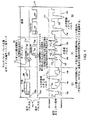
図1は、本発明の一実施形態による、正および負のイオン化パルスおよびパルス列の電圧波形を示す図である。低電圧パルス105a、105b(高電圧変圧器の入力を制御する)が、図1の上部に示される。各イオン化パルス、例えば、正のパルスが、3つの異なる電圧波成分からなる系列を含むことができる。出力パルスは、コロナ放電しきい値(図1の下部の波形110を参照)より低い振幅を有する負の電圧波で開始する。この周期の持続時間は、数マイクロ秒または数ナノ秒の範囲にある。
FIG. 1 is a diagram illustrating voltage waveforms of positive and negative ionization pulses and pulse trains according to one embodiment of the present invention.
図1に示されるように、パルス列105は、正のパルス列105aおよび負のパルス列105bを含むように配列され、列105a、105bは順次に入れ替わる。パルス列105は、エミッターに与えられる。図1は、パルス列105から生じる有効エミッター信号110も示す。
As shown in FIG. 1, the
正のパルス列105aは以下のバルス:期間115(正相115)中のTupulse_repの周期と、Tpのパルス幅とを有する複数のイオン化正電圧パルス106と、正相115後に生じる期間120(イオン化周波数相120)中のTupulse_repの周期と、To(ただし、To<Tp)のパルス幅とを有する複数のイオン化正電圧パルス107と、イオン化周波数相120後に生じる期間125(負相125)中のゼロ値とを含む。
The
負のパルス列105bは以下のパルス:期間115(正相115)中のゼロ値と、イオン化周波数相120中のTupulse_repの周期およびTo(ただし、To<Tp)のパルス幅を有する複数のイオン化負電圧パルス108であって、パルス107、108は互いにオフセットされ、同時には生成されない、複数のイオン化負電圧パルス108と、期間125(負相125)中のTupulse_repの周期およびTnのパルス幅とを有する複数のイオン化負電圧パルス109であって、TpおよびTnは時間の長さが同じである場合も、異なる場合もある、複数のイオン化負電圧パルス109とを含む。
The negative pulse train 105b has the following pulses: a plurality of ionization negative voltages having a zero value in the period 115 (positive phase 115), a period of Tupulse_rep in the
これらのイオン化正電圧パルスおよびイオン化負電圧パルスは、イオナイザーのエミッターおよび基準電極にわたって電圧勾配を生成し、コロナ放電によって、正のイオンおよび負のイオンを含むイオン雲を生成する。後に更に論じられるように、イオン化周波数相120中の正のイオン化電圧パルス107および負のイオン化電圧パルス108の結果として、有効エミッター信号110が小さな大きさの交流パルス130を有するようになる。
These ionized positive and negative voltage pulses generate a voltage gradient across the emitter and reference electrode of the ionizer and a corona discharge generates an ion cloud that contains positive and negative ions. As discussed further below, as a result of the positive
期間115の場合に示されるように、波形110は、所与のイオン放出構造のための正のコロナしきい値より高い振幅を有する高い正の電圧波を含む。その期間に、イオンエミッターは、イオンエミッターと非イオン化(または基準)電極との間の間隙において正のイオンを生成する。イオンエミッターと非イオン化電極との間のこの間隙は、例えば、上記で引用された米国特許出願第13/210,267号の図6に示される。正のイオン雲はイオンエミッターから静電的に反発し、基準電極に移動する(大抵の場合に吹き飛ばされる)。
As shown for
期間125中に、コロナ放電のために必要とされる振幅よりも著しく低い振幅を有する負の電圧が生じる。この電圧は、正のイオンの移動を減速し、基準電極へのイオン損失を減少させる静電界を生成する。負の電圧の振幅は、HVPS(高電圧電源)回路内の減衰機構によって調整することができる。
During
正のイオン化パルスには、高振幅の負のパルス(図1にも示される)が後続し、そのパルスは、上記で論じられたのと同じようにして、短い期間中に負のイオン雲を生成する。イオン化パルスの繰り返し数は毎秒1000パルス〜数千パルスの範囲にすることができる。 The positive ionization pulse is followed by a high-amplitude negative pulse (also shown in FIG. 1) that causes the negative ion cloud to pass over a short period of time in the same manner as discussed above. Generate. The number of repetitions of the ionization pulse can be in the range of 1000 pulses to thousands of pulses per second.
有効エミッター信号110はイオン化パルス142、144を含み、パルス142、144には、それより小さな負および正の振動146が後続する場合がある。負および正の振動146は信号110を生成するために用いられる電源の回路共振に起因しており、本発明を制限することは決して意図してない。振動146は、例えば、米国特許出願第13/023,387号において開示されるような減衰回路を使用することによって、実質的に低減することができるか、または完全に除去することができる。
The
非イオン化パルス148、150は、イオン化パルス142、144の極性(正)と逆の極性(負)を有する。
The
図1は、一群の正および負のイオン化パルス130を同時に示す(期間115と125の間の中央の期間120)。上側の破線135は、例えば、通常、約4.0kV〜5.0kVの範囲内にある正のコロナしきい値電圧を示し、下側の破線140は、例えば、約3.75kV〜4.50kVの範囲内にある負のコロナしきい値電圧を示す。負のコロナしきい値電圧を超えるパルスが負のイオンを生成し、正のコロナしきい値電圧を超えるパルスが正のイオンを生成する。
FIG. 1 shows a group of positive and
マイクロ秒範囲にある幾つかの短い高電圧のパルス151、152、153、154、155を用いる静電荷中和のための解決策は、オゾンの発生を少なくし、エミッター表面上に蓄積される汚染物質を少なくしながら、十分なイオン化をもたらすために見つけられた。
The solution for electrostatic charge neutralization using several short
パルス列が交互の正および負の電圧波形を与えるように配列され、各パルスが第1の非イオン化電圧レベル、第2のイオン化電圧レベル、第3の非イオン化電圧レベルおよび回路共振に起因するわずかな更なる振動を有する。アナログまたは論理タイプスイッチング回路(図3を参照)が、交互の正および負のイオン化パルスの系列を与える。 The pulse train is arranged to provide alternating positive and negative voltage waveforms, each pulse having a small amount due to the first non-ionized voltage level, the second ionized voltage level, the third non-ionized voltage level and circuit resonance. Has further vibrations. An analog or logic type switching circuit (see FIG. 3) provides a series of alternating positive and negative ionization pulses.
フェライトコア変圧器における高電圧のフライバック発生(フライバックタイプ発生器によって発生する)の使用は、適度な巻数比を有し、正および負のイオン化パルスのために電圧乗算器回路を必要としない非常に小型の変圧器(例えば、約1”×1”×1”)を使用することができる簡単で、効率的で、しかも安価なイオナイザー高電圧電源を提供する。コアの半分の間に小さな間隙を有し、電圧振動を適切に減衰させるフェライトコアを使用することは、コアの磁気メモリ効果を低減し、それにより、一方または他方の極性のパルスからなる複数のイオン化パルス系列を使用できるようにする。 The use of high voltage flyback generation (generated by flyback type generators) in ferrite core transformers has a moderate turns ratio and does not require voltage multiplier circuitry for positive and negative ionization pulses Provides a simple, efficient, and inexpensive ionizer high voltage power supply that can use very small transformers (eg, about 1 ″ × 1 ″ × 1 ″). Using a ferrite core with a gap and adequately dampening voltage oscillations reduces the magnetic memory effect of the core, thereby allowing the use of multiple ionized pulse sequences consisting of pulses of one or the other polarity. To.
結果として、正および負のイオン化パルスの列(系列または群)は、約100mm〜2000mmまたはそれ以上の範囲内の長さを有する少なくとも1つのエミッター電極の場合に十分な両極性イオン化を提供する。 As a result, a train (sequence or group) of positive and negative ionization pulses provides ample bipolar ionization for at least one emitter electrode having a length in the range of about 100 mm to 2000 mm or more.
1つの極性のパルスの数は、空気流および帯電した対象物までの距離によって決まる最良の物体中和放電時間を得るために調整することができる。交互の極性のイオンの濃度は、イオン化バーが約1000mmまで、またはそれ以上の距離において移動対象物を中和するのに十分である。 The number of pulses of one polarity can be adjusted to obtain the best object neutralization discharge time, which depends on the air flow and the distance to the charged object. The concentration of alternating polarity ions is sufficient for the ionization bar to neutralize moving objects at distances up to about 1000 mm or more.
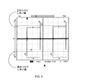
図2は、本発明の一実施形態による、リアルタイムドメインにおける例示的な列の正および負のイオン化パルスの電圧波形のスコープスクリーンショットを示す図である。図2において見られるように、パルス列対18は、順次に入れ替わる正のパルス列30および負のパルス列32を含む。上側の破線44は、正のコロナしきい値電圧(例えば、4.5kV)を表し、下側の破線46は、負のコロナしきい値電圧(例えば、-4.25kV)を表す。正のコロナしきい値電圧レベル44および負のコロナしきい値電圧レベル46はリアルタイムドメインにおいて示される。各正のパルス列30は、コロナ放電によって正のイオンを生成するための電圧しきい値を超える最大の正の電圧振幅を有するイオン化正電圧波形を含むように配列される。同様に、負のパルス列32は、コロナ放電によって負のイオンを生成するための電圧しきい値を超える最大の負の電圧振幅を有するイオン化負電圧波形を含むように配列される。このようにして、これらの正および負のそれぞれのイオン化電圧波形は、エミッターと基準電極との間の空間にわたって電圧勾配を交互に生成し、コロナ放電によって、正のイオンおよび負のイオンを含むイオン雲を生成する。
FIG. 2 is a diagram illustrating a scope screenshot of an exemplary column positive and negative ionization pulse voltage waveform in the real-time domain, in accordance with one embodiment of the present invention. As seen in FIG. 2, the pulse train pair 18 includes a positive pulse train 30 and a negative pulse train 32 that are sequentially switched. The upper dashed
パルス繰り返し数は、必要とされるイオン化電力レベルおよび移動対象物の速度に応じて調整することができる。このスクリーンショットは、高電圧電源「オン」と電源「オフ」との実効的な比を約0.0015以下にできることを例示する。そのため、本発明の一実施形態において開示されるイオン化方法によれば、コロナ放電は通常、イオン生成のために必要な時間のわずかな部分のみ(約0.1%未満)にわたって存在し、オゾンを放出するのにかかる時間、および粒子をイオンエミッターに引き寄せるのにかかる時間より短い。 The number of pulse repetitions can be adjusted according to the required ionization power level and the speed of the moving object. This screenshot illustrates that the effective ratio of high voltage power “on” to power “off” can be about 0.0015 or less. Therefore, according to the ionization method disclosed in one embodiment of the present invention, the corona discharge is usually present for only a small portion (less than about 0.1%) of the time required for ion generation, Less than the time it takes to release and the time it takes to attract the particles to the ion emitter.
1ワイヤタイプイオン化システム(またはイオン化セル)による実験は、マイクロイオン化パルスを用いる電圧波形が、概ね等しい電荷中和効率において、オゾンの放出を約3分の1〜5分の1に削減することを示した。例えば、AC高周波数電源によって電力を供給される、米国特許出願公開第2008/0232021号において記述されるのに類似のイオナイザーは、本発明の一実施形態による、同じイオナイザーの場合の約10ppb(parts-per-billion)〜15ppbと比べて、約50ppb以上のオゾン濃度を生成する。 Experiments with one-wire type ionization systems (or ionization cells) have shown that voltage waveforms using micro ionization pulses reduce ozone emissions by about 1/3 to 1/5 at approximately equal charge neutralization efficiency. Indicated. For example, an ionizer similar to that described in US Patent Application Publication No. 2008/0232021, powered by an AC high frequency power supply, is approximately 10 ppb (parts) for the same ionizer according to one embodiment of the present invention. -per-billion) Generates ozone concentration of about 50ppb or more compared to ~ 15ppb.
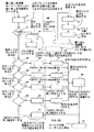
図3aは、1ワイヤタイプのエミッター電極305を備えるイオン化バーの場合の本発明のアナログ/論理ベース300の実施形態の回路図である。さらに、図3bは、図3aにおける種々の構成要素の種々の入力への波形図を示す。ガス源310がガス流を供給するように配置され、電圧源V+に電気的に結合される。パルス列105(図1に示されるように、正のパルス列105aおよび負のパルス列105bによって形成される)がエミッター305によって受信される。
FIG. 3a is a circuit diagram of an embodiment of the analog /
電源306は、アナログ/論理ベース300の一部とすることができるか、またはベース300内の構成要素に電力を供給する別の構成要素とすることができる。図面において明確にするために、基準ノード(グラウンド等)は図3aにおいて省略される。図3a内の構成要素(例えば、抵抗器、インダクターおよびキャパシターのような受動素子)の値は、本発明の実施形態を制限することを決して意図していない。
The
アナログ/論理ベース300の回路動作において、タイマーチップ(U3)315が、デュアル遅延論理チップ(U1)320、加算器論理チップ(U2)325、トランジスタ(Q1)330および(Q2)335、並びにスイッチング回路340によって形成されるパルス駆動回路317(または電源317)に短いパルスを与える。トランジスタ330、335は、例えば、MOSFETとすることができる。しかしながら、MOSFET(例えば、n−チャネルMOSFETまたは他のMOSFETタイプのトランジスタ)の使用は、本発明の実施形態を制限することを決して意図していない。
In the circuit operation of the analog /
高電圧出力変圧器345からの高電圧パルスのタイミングは最初に、台形発振器(U1)320によって生成されるクロック信号によって決まる。その発振周波数は、動作周波数と呼ばれる、正のパルス発生から負のパルス発生への交互の切り替えを決定する。その周波数は、固定キャパシター(C1)346および調整可能抵抗器(R1)347によって決定される。約0.2ヘルツ〜60ヘルツの周波数範囲が一般に用いられており、低い周波数は或る距離にある対象物に対して用いられ、高い周波数ほど近い距離にある対象物に対して用いられる。
The timing of the high voltage pulse from the high
発振器(U1)320からの出力信号は遅延デバイス(U2)325に供給され、遅延デバイスは、その周波数の半分の逆位相信号を生成する。その後、デバイス(U2)325からの出力は、ANDゲート(U4)340に供給され、ANDゲートはトランジスタ330、335(例えば、MOSFET駆動トランジスタ(Q1)330および(Q2)335)において起こり得る起動を反転させるために用いられる。
The output signal from the oscillator (U1) 320 is supplied to a delay device (U2) 325, which generates an antiphase signal at half its frequency. The output from device (U2) 325 is then provided to AND gate (U4) 340, which activates possible activations in
主起動パルスはタイマーデバイス(U3)315によって生成される。(タイマーデバイス315の)出力ピンからのフィードバック(信号351)が、そのトリガピン2およびしきい値ピン6にフィードバックされる。これにより、出力ピン3において、非常に短い正のパルスを生成できるようになる。パルス幅は、固定キャパシター(C2)350および調整可能抵抗器(R3)352によって制御される。パルス幅は、フライバック出力ドライバー317の設計に依拠して、一般的に約2マイクロ秒〜24マイクロ秒に調整される。パルスの繰り返し数は、固定キャパシター(C2)350および可変抵抗器(R4)354によって決定される。繰り返し数は、パルス周期の逆数に等しい。このパルス繰返し数は、約20ヘルツから1000ヘルツに及ぶことができ、それにより、高電圧発生器の電力出力が決まり、通常は約250ヘルツである。
The main activation pulse is generated by the timer device (U3) 315. Feedback (signal 351) from the output pin (of timer device 315) is fed back to its
ANDゲート(U4)340はフリップフロップ信号と、チップ(U3)315からのマイクロ秒幅パルスとを混合し、それにより、ドライバートランジスタ(Q1)330および(Q2)335のゲートに起動パルスを交互に印加する。 The AND gate (U4) 340 mixes the flip-flop signal and the microsecond pulse from the chip (U3) 315, thereby alternating the activation pulses to the gates of the driver transistors (Q1) 330 and (Q2) 335. Apply.
(チップ(U1)320のコンパレーター356の)ピン7からの1つの出力位相を用いて、チップ(U3)315内の発振を停止し、それにより、チップ(U3)315のピン3からの出力パルスを中断する。この中断を用いて、正のイオン化と負のイオン化との間のオフタイムを与えることができる。この中断は、場合によっては、長い対象物距離におけるイオン雲再結合を減少させるか、または単に電力出力を低減するために用いられる。オフタイムまたはデッドタイムは、ピン10、13(それぞれ、チップ(U1)320内のコンパレーター358、359)に印加されるバイアスによって調整される。
One output phase from pin 7 (of
マイクロパルスの形成は、以下の動作によって達成される。一例として、MOSFET(Q2)335のゲートへの短い正のパルス(マイクロ秒範囲)によって、高電圧変圧器345の一次巻線コイル(2、3)360内に電流が流れ、それにより最初に、一次巻線コイル360の両端に小さな負の電圧パルスを生成する。負の電圧パルスの終了時に、回路共振に起因する小さな負および正の振動とともに、大きな正の電圧のフライバックパルスが生成される。
The formation of the micropulse is achieved by the following operation. As an example, a short positive pulse (microsecond range) to the gate of MOSFET (Q2) 335 causes a current to flow in the primary winding coil (2, 3) 360 of
代替的には、MOSFET(Q1)330のゲートへの短いパルスが大きな負のパルスを生成する。これらのパルス電圧は、約50〜500対1程度とすることができる大きな巻数比を用いることによって、変圧器345の二次巻線362によって拡大され、位相反転される。このようにして、MOSFET(Q2)335は、負の高電圧パルスを開始し、MOSFET(Q1)330は正の高電圧パルスを開始する。これらのパルスは、同じワイヤまたは尖端エミッターによって正のイオンおよび負のイオンを生成する。
Alternatively, a short pulse to the gate of MOSFET (Q1) 330 produces a large negative pulse. These pulse voltages are magnified and phase inverted by the secondary winding 362 of
正負両方の極性の場合のパルス電圧振幅は以下のパラメーターによって決定される。
1.変圧器(T1)345の巻線比
2.変圧器一次コイル360のインダクタンス
3.トランジスタ330、335のゲートに導入されるMOSFETゲートパルスの持続時間
4.電解フィルターであるキャパシター364において見られるような入力DC電圧
5.減衰回路抵抗器365(例えば、2オームの抵抗)、インダクター367(例えば、22μHのインダクタンス)および一次コイル360にかかるシャント抵抗器(Rp)368によって形成される一次減衰回路363
6.直列に接続されるトランジスタ330、335(例えば、MOSFET(Q1)330および(Q2)335)の抵抗
7.イオン化アセンブリの容量性負荷(変圧器二次巻線362の出力において測定される)
The pulse voltage amplitude for both positive and negative polarities is determined by the following parameters.
1. 1. Turn ratio of transformer (T1) 345 2. Inductance of transformer
6). 6. Resistance of
変圧器(T1)345からの高電圧出力パルスは、一次巻線360のインダクタンス、および減衰回路363の二次および一次減衰構成要素上の容量性負荷によって設定される波形を有する。変圧器中心タップ2と電力入力(Vin)との間に配置されるシャント抵抗器(Rs)365およびインダクター(Ls)367は、変圧器345内の電流の急激な立ち上がり時間を防ぎ、それにより、波形110(図1)の第1の部分(図1の部分115)のピーク値を減少させる。波形110の第3の部分(図1)は、シャント抵抗器(Rs)365によって低減される。これらの構成要素を選択的に、または注意深く調整する結果として、波形110の第2の部分120(図1)の高いピークレベルの要件を超える最大イオン化効率が得られる。
The high voltage output pulse from transformer (T1) 345 has a waveform set by the inductance of primary winding 360 and the capacitive load on the secondary and primary attenuation components of
再び図2を参照すると、生成されたパルスの高いスルーレートが見られる。一次コイル360の場合、電圧立ち上がり速度は約270V/μsであり、立ち下がり速度は約1800V/μsである。二次コイル362の場合、スルーレートは約35(±8)kV/μsまで上昇する場合がある。いかなる乗算器、整流器および加算ブロックも用いることなく、1つの小出力高電圧変圧器345だけを用いて、駆動回路317によって非対称の正および負のパルスを絶えず生成することができる。
Referring again to FIG. 2, a high slew rate of the generated pulses can be seen. In the case of the
中和対象物の電荷密度および速度に応じて、パルス繰り返し数を調整できることにも留意されたい。当該技術分野(複数の場合もある)の当業者に既知である信号伝送(例えば、電流信号または電圧信号)に関する他の詳細は、本発明の実施形態に焦点を合わせるために、更には論じられない。ACコロナイオナイザーにおいて生じる種々の標準的な信号伝送は、上記で引用された参考文献において更に詳述される。波形は、全ての構成要素の抵抗、キャパシタンスおよびインダクタンス(それぞれR、C、L)の値によって定められる。パルス高は、デバイス(U3)315に関連付けられる抵抗器(R3)352およびキャパシター(C2)350によって図3において設定されるパルス持続時間を変更することによって調整することができる。 It should also be noted that the pulse repetition rate can be adjusted depending on the charge density and speed of the neutralization object. Other details regarding signal transmissions (eg, current signals or voltage signals) known to those skilled in the art (s) are further discussed to focus on embodiments of the present invention. Absent. The various standard signal transmissions that occur in an AC coronizer are further detailed in the references cited above. The waveform is defined by the resistance, capacitance, and inductance values (R, C, L, respectively) of all components. The pulse height can be adjusted by changing the pulse duration set in FIG. 3 by resistor (R3) 352 and capacitor (C2) 350 associated with device (U3) 315.
図4a、4bは、本発明のマイクロプロセッサに基づく実施形態のブロック図である。図4aに示されるように、パルス駆動回路は、トランジスタ330のスイッチングを制御するためのマイクロコントローラ400(または他のプロセッサ若しくはコントローラ400)を含む。マイクロコントローラ400は、ソフトウェアの制御下で、通常、約19マイクロ秒幅の、ソフトウェアによって調整された狭いパルスを生成し、1つのパルス列402aが正のイオン化パルスに割り当てられ、1つのパルス列402bは負のイオン化パルスに割り当てられる。マイクロコントローラ400から、パルスは、例えば、高電力MOSFETとすることができるスイッチングトランジスタ330、335(図3a)を駆動するのに適した大きさにパルスを増幅する1組のパルスドライバー405(図4b)に加えられる。上記で論じられたように、これらのMOSFETは、その後、高電圧パルス変圧器345を駆動する。
4a and 4b are block diagrams of an embodiment based on the microprocessor of the present invention. As shown in FIG. 4 a, the pulse drive circuit includes a microcontroller 400 (or other processor or controller 400) for controlling the switching of
本発明の他の実施形態において除外することができるオプションとして、マイクロコントローラ400は、スパーク検出器410および断線検出器425からそれぞれ信号410、415を受信することもできる。図3a、4aおよび/または本明細書における他の図/図面において示される実施形態のいずれかにおいて、印加される電力が、コロナ放電によって正のイオンおよび負のイオンを生成するのに十分であるが、オゾンおよび酸化窒素を生成する、エミッターを腐食する、および周囲空気からの粒子を引き寄せるには不十分であるように、パルス持続時間を短くすることができる。図3a、4aおよび/または本明細書における他の図/図面において示される実施形態のいずれかにおいて、そのイオナイザーは、通常の約50000ヘルツ〜70000ヘルツの代わりに、例えば、約250ヘルツ(またはそれ未満)のような非常に遅い繰り返し数において、イオン化しきい値より少なくとも約1000ボルト高い強い(または相対的に強い)イオン化パルスを与え、それにより、オゾンを少なく抑えながらイオンを生成する。
As an option that may be excluded in other embodiments of the present invention, the
図5a、5b、5cは、異なる電荷中和条件の場合に高電圧波形(パルス列)を最適化する3つの異なるモードのマルチパルスを示し、図5dは、本発明の一実施形態による、マイクロコントローラ400によって実行されるソフトウェアによって実行される方法を示す。モードA、BおよびA+Bは、例えば、正の電荷および負の電荷に対する放電時間、許容可能な電圧の揺れ(電界効果)、対象物までの距離のような、電荷中和要件によって決まる。マイクロコントローラ400は、本発明の実施形態を実施するアプリケーションによって要求されるようなイオン化パルスの3つのモード:モードA、モードBおよびモードA+Bを与えることができるソフトウェアを実行する。
FIGS. 5a, 5b, 5c show three different modes of multi-pulses that optimize the high voltage waveform (pulse train) for different charge neutralization conditions, and FIG. 5d shows a microcontroller according to one embodiment of the present invention. 4 illustrates a method performed by software executed by 400. Modes A, B, and A + B depend on charge neutralization requirements such as discharge time for positive and negative charges, acceptable voltage swing (field effect), distance to the object, etc. The
モードA:図5aに示されるように、モードAは、正のパルスおよび負のパルスの組み合わせの反復系列によって規定される。各正のパルス505(正のコロナしきい値506aを超える)の後に負のパルス510(負のコロナしきい値506bを超える)が続き、その後、各負のパルス510の後に正のパルス505が続く。正のパルス列515aおよび負のパルス列515bが示されており、正の電圧パルスおよび負の電圧パルスが交互に生じる。このモードは通常、イオン化フィールド電圧を小さくする必要がある非常に近い対象物距離(例えば、約200mm以下)において用いられる。
Mode A: As shown in FIG. 5a, Mode A is defined by a repeating sequence of combinations of positive and negative pulses. Each positive pulse 505 (beyond the positive corona threshold 506a) is followed by a negative pulse 510 (beyond the
モードAでは、マイクロコントローラ400によって実行されるソフトウェアによって、正のマイクロパルス505および負のマイクロパルス510のパルス振幅529、マイクロパルス周期525並びにパルス幅530、535がそれぞれ調整可能である。正のマイクロパルス振幅および正のマイクロパルス持続時間は、ブロック563(図5d)において、タイマー/カウンタによってロードパルスMP_P値により調整される。負のマイクロパルス振幅および負のマイクロパルス持続時間は、ブロック566(図5d)においてロードパルスMP_Nによって調整される。正のマイクロパルスおよび負のマイクロパルスのための周期は、ブロック551(図5d)において、ロード繰り返し周波数(Reprate)タイマー/カウンタによって繰り返し周波数値により調整される。
In mode A, the pulse amplitude 529, the
モードB:図5bに示されるように、モードBは、図示されるように、正のパルス541の反復系列540の後に負のパルス543の反復系列542が続き、その後に正のパルス541の反復系列540が続き、それを繰り返すことによって規定される。正のパルス系列540と負のパルス系列542との間に、小さな遅延544、すなわちオフタイムを加えて、イオン再結合を低減することができる。オフタイムは、イオン化パルスが生成されない時間である。このモードは通常、非常に遠い(500mm以上の)対象物距離において用いられる。ブロック554(図5d)にロードされるブロック568(図5d)のMP_N値の数を用いて、パルスが生成されないオフタイム遅延値544(図5b)を設定する。正のイオン化パルス幅は、ブロック556(図5d)においてロードパルスタイマー/カウンタによってTpmax値により調整される。正のイオン化パルス周期は、ブロック551(図5d)においてロード繰り返し周波数タイマー/カウンタによって繰り返し周波数値により調整される。負のイオン化パルス幅は、ブロック560(図5d)においてロードパルスタイマー/カウンタによってTnmax値により調整される。負のイオン化パルス周期は、ブロック551(図5d)においてロード繰り返し周波数タイマー/カウンタによって繰り返し周波数値により調整される。
Mode B: As shown in FIG. 5b, mode B includes a
モードA+B:図5cに示されるように、モードA+Bは、モードAとモードBとの組み合わせであり、モードAはオフタイム領域(時間)550において生じ、モードBはオンタイム領域(時間)551、552において生じる。このモードは通常、イオン化フィールド電圧は低くしておく必要があるが、対象物距離はプロセスに応じて変化する、中間距離(200mm〜500mm)の対象物において用いられる。オンタイム領域551、553はブロック554において調整される。オフタイム領域550は、この領域の幅を決定する(すなわち、ブロック554において設定される)パルスMP_PおよびパルスMP_Nの数によって調整される。正のマイクロパルス幅はブロック563によって調整される。負のマイクロパルス幅はブロック566によって調整される。負のイオン化パルス幅はブロック560によって決定される。負のパルス繰り返し数はブロック551によって決定される。図5dは、マイクロコントローラ400によって実行されるソフトウェアによって実行される方法574の他の機能を記述する種々のブロック550〜573を示す。図5eは、本発明の一実施形態による、マルチパルス設定可能パラメーターおよび対応する定義、並びに例示的なパラメーター範囲値を示す表575である。図5f、図5g、5hも、本発明の一実施形態による、図5a、図5b、5cとは異なる設定に基づく3つの異なるモードにおけるマルチパルスを示す。
Mode A + B: As shown in FIG. 5c, mode A + B is a combination of mode A and mode B, mode A occurs in off-time region (time) 550, mode B is on-time region (time) 551, Occurs at 552. This mode is typically used for objects at intermediate distances (200 mm to 500 mm) where the ionization field voltage needs to be kept low, but the object distance varies with the process. On-
全ての3つのモードにおいて、ユーザは、(1)正若しくは負または両方のパルス幅を変更し、オフタイム領域(MP_P、MP_N)から独立してオンタイム領域(TpmaxおよびTnmax)におけるイオン化量を制御することによって、かつ(2)正のオンタイム領域と負のオンタイム領域との間の時間比を変更することによって、イオンバランスを変更することができる。パルス間の時間(Treprate)は全ての領域において同じであり、イオン化電力量を制御するために調整可能である。高い電力は、Treprateが小さな場所であり、より頻繁にイオン化パルスを生成し、結果として、より多くのイオン化が生じる。一方、Treprateが大きいほど、イオン化パルスが生成される頻度が小さくなり、結果としてイオン化が少なくなる。 In all three modes, the user can (1) change the positive or negative pulse width or both to control the ionization amount in the on-time region (Tpmax and Tnmax) independently of the off-time region (MP_P, MP_N) And (2) the ion balance can be changed by changing the time ratio between the positive on-time region and the negative on-time region. The time between pulses (Treprate) is the same in all regions and can be adjusted to control the ionization power. High power is a place where the Treprate is small and produces more frequent ionization pulses, resulting in more ionization. On the other hand, the greater the Treprate, the less frequently the ionization pulses are generated, resulting in less ionization.
それゆえ、本発明の一実施形態は、イオン化の方法および関連する回路図(装置)を提供する。この実施形態は、非常に短い両極性マイクロパルスを生成し、通常の大気圧において通常のエミッターを用いて効率的な両極性空気(または他のガス)イオン化をもたらす。 Therefore, one embodiment of the present invention provides a method of ionization and an associated circuit diagram (apparatus). This embodiment produces very short bipolar micropulses and provides efficient bipolar air (or other gas) ionization with a normal emitter at normal atmospheric pressure.
図8に示される実施形態では、高電圧パルス発生器が、種々のイオンエミッター:単一または一群のワイヤ、鋸刃タイプエミッター、尖端電極(複数の場合もある)を備えた種々のイオン化セル(構造)に電力を供給することができる。また、イオン化バーは、イオンエミッターに極めて近接して配置されるノズル、小径のオリフィスまたはスロットに接続される空気流の内部供給源(空気チャネル)を有することができる。それゆえ、図8は、本発明の一実施形態による、ワイヤエミッターおよび空気支援イオン送達システムを備える線形バーの概略図を示す。 In the embodiment shown in FIG. 8, the high voltage pulse generator includes various ion emitters: single or group of wires, saw blade type emitters, various ionization cells with tip electrode (s). Power). The ionization bar can also have an internal source of air flow (air channel) connected to a nozzle, small diameter orifice or slot located in close proximity to the ion emitter. Therefore, FIG. 8 shows a schematic diagram of a linear bar comprising a wire emitter and an air assisted ion delivery system, according to one embodiment of the present invention.
本発明の別の実施形態は、主にイオン化バー設計に関する。図6(図6a、6b)は、2つの(ワイヤおよび先端タイプ)エミッター電極E1およびE2を備える二相イオン化バーとしての本発明の別の実施形態の概略図を示す。2つのエミッターを備えるこの二相イオナイザーでは、エミッターはいずれも、鋭い尖端電極、ワイヤ若しくは刃の列として、または尖端エミッターを備えるノズルの列として構成することができる。線形バー内の要素の更なる詳細が、上記で引用された米国仮特許出願第61/584,173号に開示されている。 Another embodiment of the invention relates primarily to ionization bar design. FIG. 6 (FIGS. 6a, 6b) shows a schematic diagram of another embodiment of the present invention as a two-phase ionization bar comprising two (wire and tip type) emitter electrodes E1 and E2. In this two-phase ionizer with two emitters, any emitter can be configured as a sharp tip electrode, a row of wires or blades, or as a row of nozzles with a tip emitter. Further details of the elements within the linear bar are disclosed in the above-cited US Provisional Patent Application No. 61 / 584,173.
高電圧セクションの設計は、MOSFETの場合と同じドライバー回路(上記で論じられた)を用いるが、MOSFETトランジスタドレイン(M1およびM2)が、一対の高電圧変圧器T1、T2の一次側に逆向きに接続されている。 The high voltage section design uses the same driver circuit (discussed above) as the MOSFET, but the MOSFET transistor drains (M1 and M2) are reversed to the primary side of a pair of high voltage transformers T1, T2. It is connected to the.
制御抵抗器R1および減衰キャパシターC2(図6)が、図3に示される回路設計の場合と同じ交互極性パルスを生成するように選択される。それゆえ、各パルスは、主に正または負のピーク振幅を有し、極性が入れ替わる。 Control resistor R1 and attenuation capacitor C2 (FIG. 6) are selected to produce the same alternating polarity pulses as in the circuit design shown in FIG. Therefore, each pulse has a predominantly positive or negative peak amplitude and the polarity is reversed.
図7において、キャパシターC2が、変圧器T1、T2の底部系統部分と直列に接続されることによって、イオン化システムが自己バランスモードにおいて動作できるようになる。両方のイオンエミッターがグラウンドに対して相対的に浮いており、電荷保存の法則によれば、出力イオン雲はかなり良好に平衡が保たれることになる。そうでない場合には、任意の通常の不平衡が、キャパシターC2の両端に反対のDC電圧を生成する。上記のバランスを得るための方法に関する更なる詳細は、共同所有で、同じ譲受人に譲渡された、Leslie W. Partridgeによる米国特許第5,055,963号において確認することができ、米国特許第5,055,963号は引用することにより本明細書の一部をなす。 In FIG. 7, the capacitor C2 is connected in series with the bottom system portion of the transformers T1, T2, allowing the ionization system to operate in a self-balancing mode. Both ion emitters are floating relative to the ground, and according to the law of charge conservation, the output ion cloud will be fairly well balanced. Otherwise, any normal imbalance will produce an opposite DC voltage across capacitor C2. Further details on how to achieve the above balance can be found in US Pat. No. 5,055,963 by Leslie W. Partridge, co-owned and assigned to the same assignee, which is cited To form part of this specification.
変圧器T1、T2に接続されるイオンエミッターは、正反対の極性を有する電圧のイオン化パルスを有する。この二相イオン化システムの場合の電圧波形602が(図6a)に示されており、エミッター(1)E1およびエミッター(2)E2を備える簡略化されたバーの断面605が(図6b)に示される。
The ion emitters connected to the transformers T1, T2 have voltage ionization pulses with opposite polarities. The voltage waveform 602 for this two-phase ionization system is shown in (FIG. 6a) and a
図6のこの実施形態は、単相イオン化システムに比べて、少なくとも2つの利点を有する。多くの場合に、電荷中和の物体は電界に影響されやすく、電界を相殺する効果があるイオナイザーを有する必要がある。二相イオン化システムは、逆極性の電圧を同時に生成し、それにより、放射される電界を著しく低減する。 This embodiment of FIG. 6 has at least two advantages over the single phase ionization system. In many cases, charge neutralizing objects are sensitive to electric fields and need to have an ionizer that has the effect of canceling out the electric field. A two-phase ionization system simultaneously generates voltages of opposite polarity, thereby significantly reducing the radiated electric field.
この特徴は、イオン化バーが帯電した物体に極めて近接して配置されることになる場合にも重要である。例えば、正のパルス列の持続時間(パルス持続時間、振幅またはパルス周波数等)の場合のイオン化バーと物体との間の距離に関して、その距離は、1つのエミッターの場合の1サイクル内の負のパルス列の場合より長い場合があり、次の1サイクルでは、逆極性が飽和状態になる場合がある。それはイオン雲の「押す」効果をもたらし、対象物へのイオンの移動を加速することになる。 This feature is also important when the ionization bar is to be placed in close proximity to a charged object. For example, with respect to the distance between the ionization bar and the object in the case of a positive pulse train duration (pulse duration, amplitude or pulse frequency, etc.), the distance is the negative pulse train in one cycle for one emitter. The reverse polarity may become saturated in the next one cycle. It brings about the “push” effect of the ion cloud and accelerates the movement of ions to the object.
二相イオン化システムは、かさばる基準電極を全く有せず、これらの電極におけるイオン損失を回避するという別の利点を有する。 Two-phase ionization systems do not have any bulky reference electrodes and have the additional advantage of avoiding ion loss at these electrodes.
さらに、逆相の電圧源は、コロナ放電を生成するために各エミッターにおいて必要とされる電圧振幅を著しく(概ね2分の1に)減少させることができる。それゆえ、これらの変圧器は同じ設計にすることができるか、または低い一次対二次巻数比を有することができる。互いに近接しているとき、エミッターはエミッター対間の電界を高める傾向があるので、低い巻数比を用いることができる。 In addition, the out-of-phase voltage source can significantly (approximately half) reduce the voltage amplitude required at each emitter to generate a corona discharge. Therefore, these transformers can be of the same design or have a low primary to secondary turns ratio. When in close proximity to each other, emitters tend to increase the electric field between the emitter pair, so a low turns ratio can be used.
図6は、各エミッターが変圧器T1、T2の出力に容量性結合される(C3、C4)二相線形イオナイザーの実施形態も示す。両方の変圧器T1、T2の二次コイルは接地される。これは、容量性結合による自己バランス型イオン化システムの別の変形形態である。 FIG. 6 also shows an embodiment of a (C3, C4) two-phase linear ionizer in which each emitter is capacitively coupled to the outputs of transformers T1, T2. The secondary coils of both transformers T1, T2 are grounded. This is another variation of a self-balancing ionization system with capacitive coupling.
図3に示される実施形態と図6に示される実施形態との間の違いは主に、イオンバランスオフセットへの反応時間である。キャパシター(C3、C4)は、バランスをとるのに短い移行時間を与えることができる。各エミッターに直列に接続される小さなキャパシターは、エミッター間の位相シフトを微調整し、エミッターが接触する場合に電流を制限するのを助けることができる。 The difference between the embodiment shown in FIG. 3 and the embodiment shown in FIG. 6 is mainly the reaction time to the ion balance offset. Capacitors (C3, C4) can provide a short transition time to balance. A small capacitor connected in series with each emitter can fine tune the phase shift between the emitters and help limit the current when the emitters are in contact.
イオンバランス制御:
一実施形態では、イオナイザーは、幾つかの異なる変形形態(図7に示される)の自己バランスシステムを有することができ、ワイヤエミッター(破線705によって示される)が、HVPS出力に容量性結合し、基準電極に接地することができ、浮いている変圧器二次側のエミッターおよび基準はいずれもHVPSに容量性結合される。
Ion balance control:
In one embodiment, the ionizer can have a number of different variations (shown in FIG. 7) self-balancing system, where a wire emitter (indicated by dashed line 705) is capacitively coupled to the HVPS output, The floating transformer secondary emitter and reference can both be grounded to the reference electrode and capacitively coupled to the HVPS.
また、線形イオナイザーは帯電した対象物に極めて近接して配置される外部イオンバランスセンサー(複数の場合もある)を用いるアクティブイオンバランスシステムを有することもできる。この場合、マイクロプロセッサに基づく制御システムおよびバーのHVPSが主にイオン化マイクロパルスを生成し、対象物の電荷と逆極性のイオンを生成することができる。 The linear ionizer can also have an active ion balance system that uses an external ion balance sensor (s) that is placed in close proximity to the charged object. In this case, the microprocessor-based control system and the bar HVPS can mainly generate ionized micropulses and generate ions of opposite polarity to the charge of the object.
ワイヤタイプエミッターを備える線形イオン化バーの概略図が図8に示される。ワイヤ電極801がばね802によってバーのシャーシ(またはカートリッジ)に取り付けられる。ばね802はワイヤ張力を与え、上記で論じられた高電圧電源(図8に示されない)の出力に接続される。基準電極803は、シャーシの両側に取り付けられる2つのステンレス鋼ストリップとして構成される。高い強度の電界が、ワイヤエミッターを覆うイオンプラズマシースの形においてコロナ放電を生成する。
A schematic diagram of a linear ionization bar with a wire-type emitter is shown in FIG. A
空気口804が、エミッターによって生成されたイオンが対象物まで移動するのを助ける空気流を供給する。それゆえ、イオンは、電界および空気力の組み合わせによって帯電した対象物まで移動する。その結果、対象物の電荷を中和するための放電時間が短くなる(数秒の範囲内)。
本発明は特定の実施形態において説明されてきたが、本発明がそのような実施形態によって限定されるように解釈されるべきでないことは理解されたい。むしろ、本発明は添付の特許請求の範囲に従って解釈されるべきである。 Although the invention has been described in certain embodiments, it should be understood that the invention is not to be construed as limited by such embodiments. Rather, the present invention should be construed according to the claims that follow.
300 論理ベース
300 ベース
305 エミッター電極
305 エミッター
306 電源
310 ガス源
315 タイマーチップ(U3)
315 タイマーデバイス(U3)
315 タイマーデバイス
315 チップ(U3)
315 デバイス(U3)
317 パルス駆動回路
317 電源
317 フライバック出力ドライバー
317 駆動回路
320 デュアル遅延論理チップ(U1)
320 台形発振器(U1)
325 遅延デバイス(U2)
330 MOSFET(Q1)
335 MOSFET(Q2)
340 ゲート(U4)
345 高電圧出力変圧器
346 固定キャパシター(C1)
347 調整可能抵抗器(R1)
350 固定キャパシター(C2)
352 調整可能抵抗器(R3)
354 可変抵抗器(R4)
356 コンパレーター
358 コンパレーター
359 コンパレーター
360 変圧器一次コイル
362 変圧器二次コイル
363 一次減衰回路
364 キャパシター
365 シャント抵抗器(Rs)
367 インダクター(Ls)
368 シャント抵抗器(Rp)
400 マイクロコントローラ
405 パルスドライバー
410 スパーク検出器
425 断線検出器
300
315 Timer device (U3)
315
315 devices (U3)
317
320 Trapezoidal oscillator (U1)
325 delay device (U2)
330 MOSFET (Q1)
335 MOSFET (Q2)
340 Gate (U4)
345 High Voltage Output Transformer 346 Fixed Capacitor (C1)
347 Adjustable Resistor (R1)
350 Fixed Capacitor (C2)
352 Adjustable resistor (R3)
354 Variable resistor (R4)
367 Inductor (Ls)
368 Shunt resistor (Rp)
400 Microcontroller 405
Claims (13)
持続時間の短い鋭いマイクロパルスを生成し、
各マイクロパルスが正電圧部分と負電圧部分とを含み、
前記マイクロパルスが、正電圧および負電圧の大きさおよび振幅に関して非対称であり、
少なくとも1つの極の電圧の大きさがコロナしきい値を超えており、
パルス列が複数の波を含んでおり、各波は、初期の低い振幅ピークと、逆極性の第2の高い振幅ピークと、最後の低い振幅ピークとを含み、
前記パルスは、電荷中和対象物の移動速度及び電荷中和対象物とエミッタの距離によって、パルス数、持続時間、繰り返し数および振幅を可変にした両極性パルス列をなしているようにした方法。 In a method for charge neutralization by generating bipolar ions during corona discharge between an emitter and a reference electrode,
Produces sharp micropulses with short duration,
Each micropulse includes a positive voltage portion and a negative voltage portion,
The micropulse is asymmetric with respect to the magnitude and amplitude of the positive and negative voltages;
The voltage magnitude of at least one pole exceeds the corona threshold,
The pulse train includes a plurality of waves, each wave including an initial low amplitude peak, a second high amplitude peak of opposite polarity, and a last low amplitude peak;
The pulse is a bipolar pulse train in which the number of pulses, the duration, the number of repetitions, and the amplitude are variable depending on the moving speed of the charge neutralization object and the distance between the charge neutralization object and the emitter .
持続時間の短い鋭いマイクロパルスを生成するパルス駆動回路を具備し、
各マイクロパルスが正電圧部分と負電圧部分とを含み、
前記マイクロパルスが、正電圧および負電圧の大きさおよび振幅に関して非対称であり、
少なくとも1つの極の電圧の大きさがコロナしきい値を超えるようにし、
パルス列が複数の波を含んでおり、各波は、初期の低い振幅ピークと、逆極性の第2の高い振幅ピークと、最後の低い振幅ピークとを含み、
前記パルス駆動回路が、電荷中和対象物の移動速度及び電荷中和対象物とエミッタの距離によって、パルス数、持続時間、繰り返し数および振幅を可変にした両極性パルスを生成するようにした装置。 In an apparatus that generates bipolar ions during corona discharge between an emitter and a reference electrode,
Comprising a pulse driving circuit for generating sharp micropulses having a short duration;
Each micropulse includes a positive voltage portion and a negative voltage portion,
The micropulse is asymmetric with respect to the magnitude and amplitude of the positive and negative voltages;
Ensure that the voltage magnitude of at least one pole exceeds the corona threshold;
The pulse train includes a plurality of waves, each wave including an initial low amplitude peak, a second high amplitude peak of opposite polarity, and a last low amplitude peak;
An apparatus in which the pulse driving circuit generates bipolar pulses with variable number of pulses, duration, number of repetitions and amplitude depending on the moving speed of the charge neutralization target and the distance between the charge neutralization target and the emitter. .
Applications Claiming Priority (3)
| Application Number | Priority Date | Filing Date | Title |
|---|---|---|---|
| US13/367,369 | 2012-02-06 | ||
| US13/367,369 US8773837B2 (en) | 2007-03-17 | 2012-02-06 | Multi pulse linear ionizer |
| PCT/US2012/064045 WO2013119283A1 (en) | 2012-02-06 | 2012-11-08 | Multi pulse linear ionizer |
Related Child Applications (1)
| Application Number | Title | Priority Date | Filing Date |
|---|---|---|---|
| JP2017203474A Division JP2018026357A (en) | 2012-02-06 | 2017-10-20 | Multi pulse linear ionizer |
Publications (3)
| Publication Number | Publication Date |
|---|---|
| JP2015511378A JP2015511378A (en) | 2015-04-16 |
| JP2015511378A5 JP2015511378A5 (en) | 2016-01-07 |
| JP6567828B2 true JP6567828B2 (en) | 2019-08-28 |
Family
ID=47427412
Family Applications (2)
| Application Number | Title | Priority Date | Filing Date |
|---|---|---|---|
| JP2014556533A Active JP6567828B2 (en) | 2012-02-06 | 2012-11-08 | Multi-pulse linear ionizer |
| JP2017203474A Pending JP2018026357A (en) | 2012-02-06 | 2017-10-20 | Multi pulse linear ionizer |
Family Applications After (1)
| Application Number | Title | Priority Date | Filing Date |
|---|---|---|---|
| JP2017203474A Pending JP2018026357A (en) | 2012-02-06 | 2017-10-20 | Multi pulse linear ionizer |
Country Status (5)
| Country | Link |
|---|---|
| EP (1) | EP2812964B1 (en) |
| JP (2) | JP6567828B2 (en) |
| KR (1) | KR101968795B1 (en) |
| TW (1) | TWI575830B (en) |
| WO (1) | WO2013119283A1 (en) |
Families Citing this family (11)
| Publication number | Priority date | Publication date | Assignee | Title |
|---|---|---|---|---|
| WO2013119283A1 (en) * | 2012-02-06 | 2013-08-15 | Illinois Tool Works Inc. | Multi pulse linear ionizer |
| US9808547B2 (en) | 2013-04-18 | 2017-11-07 | Dm Tec, Llc | Sanitizer |
| JP6334152B2 (en) * | 2013-12-11 | 2018-05-30 | シャープ株式会社 | Ion generator |
| JP5989020B2 (en) * | 2014-03-05 | 2016-09-07 | シシド静電気株式会社 | Ion generator |
| US9950086B2 (en) | 2014-03-12 | 2018-04-24 | Dm Tec, Llc | Fixture sanitizer |
| TWI652869B (en) * | 2014-03-19 | 2019-03-01 | 美商伊利諾工具工程公司 | Automatically balanced micropulse ionization blower |
| US9700643B2 (en) | 2014-05-16 | 2017-07-11 | Michael E. Robert | Sanitizer with an ion generator |
| US9084334B1 (en) * | 2014-11-10 | 2015-07-14 | Illinois Tool Works Inc. | Balanced barrier discharge neutralization in variable pressure environments |
| US10124083B2 (en) | 2015-06-18 | 2018-11-13 | Dm Tec, Llc | Sanitizer with an ion generator and ion electrode assembly |
| JP6902167B2 (en) * | 2017-08-25 | 2021-07-14 | イーグル ハーバー テクノロジーズ, インク.Eagle Harbor Technologies, Inc. | Generation of arbitrary waveforms using nanosecond pulses |
| US11310897B2 (en) | 2018-10-08 | 2022-04-19 | Illinois Tool Works Inc. | Method and apparatus for an ionized air blower |
Family Cites Families (14)
| Publication number | Priority date | Publication date | Assignee | Title |
|---|---|---|---|---|
| US3875035A (en) * | 1971-08-25 | 1975-04-01 | Purification Sciences Inc | Solid state frequency converter for corona generator |
| JPS5630283A (en) * | 1979-08-22 | 1981-03-26 | Yahata Electric Works | Charging unit with ac corona discharge |
| US5005101A (en) * | 1989-01-31 | 1991-04-02 | Gallagher James C | Method and apparatus for negative charge effect and separation of undesirable gases |
| US5055963A (en) | 1990-08-15 | 1991-10-08 | Ion Systems, Inc. | Self-balancing bipolar air ionizer |
| ATE556779T1 (en) * | 2003-06-05 | 2012-05-15 | Daikin Ind Ltd | DISCHARGE DEVICE AND AIR PURIFICATION DEVICE |
| US20060018809A1 (en) * | 2004-07-23 | 2006-01-26 | Sharper Image Corporation | Air conditioner device with removable driver electrodes |
| US7126092B2 (en) | 2005-01-13 | 2006-10-24 | Watlow Electric Manufacturing Company | Heater for wafer processing and methods of operating and manufacturing the same |
| US20070279829A1 (en) * | 2006-04-06 | 2007-12-06 | Mks Instruments, Inc. | Control system for static neutralizer |
| US7751695B2 (en) | 2006-06-12 | 2010-07-06 | Lawrence Livermore National Security, Llc | High-speed massively parallel scanning |
| US8009405B2 (en) * | 2007-03-17 | 2011-08-30 | Ion Systems, Inc. | Low maintenance AC gas flow driven static neutralizer and method |
| US7813102B2 (en) * | 2007-03-17 | 2010-10-12 | Illinois Tool Works Inc. | Prevention of emitter contamination with electronic waveforms |
| US8885317B2 (en) * | 2011-02-08 | 2014-11-11 | Illinois Tool Works Inc. | Micropulse bipolar corona ionizer and method |
| JP5046390B2 (en) | 2008-01-07 | 2012-10-10 | 株式会社キーエンス | Static eliminator |
| WO2013119283A1 (en) * | 2012-02-06 | 2013-08-15 | Illinois Tool Works Inc. | Multi pulse linear ionizer |
-
2012
- 2012-11-08 WO PCT/US2012/064045 patent/WO2013119283A1/en active Application Filing
- 2012-11-08 EP EP12805532.4A patent/EP2812964B1/en active Active
- 2012-11-08 JP JP2014556533A patent/JP6567828B2/en active Active
- 2012-11-08 KR KR1020147024139A patent/KR101968795B1/en active Active
- 2012-12-17 TW TW101147823A patent/TWI575830B/en active
-
2017
- 2017-10-20 JP JP2017203474A patent/JP2018026357A/en active Pending
Also Published As
| Publication number | Publication date |
|---|---|
| EP2812964A1 (en) | 2014-12-17 |
| TW201338321A (en) | 2013-09-16 |
| TWI575830B (en) | 2017-03-21 |
| KR101968795B1 (en) | 2019-04-12 |
| KR20140123084A (en) | 2014-10-21 |
| JP2018026357A (en) | 2018-02-15 |
| EP2812964B1 (en) | 2020-09-02 |
| JP2015511378A (en) | 2015-04-16 |
| WO2013119283A1 (en) | 2013-08-15 |
Similar Documents
| Publication | Publication Date | Title |
|---|---|---|
| JP6567828B2 (en) | Multi-pulse linear ionizer | |
| US8773837B2 (en) | Multi pulse linear ionizer | |
| EP2673092B1 (en) | Micropulse bipolar corona ionizer and method | |
| CA2355659C (en) | Electrostatic fluid accelerator | |
| US7532451B2 (en) | Electrostatic fluid acclerator for and a method of controlling fluid flow | |
| US9709017B2 (en) | Ignition device of spark-ignition internal combustion engine | |
| US20040217720A1 (en) | Electrostatic fluid accelerator for and a method of controlling fluid flow | |
| CN100552854C (en) | Method and apparatus for electrostatic fluid acceleration control of fluid flow | |
| JP2005222779A (en) | Plasma processing device | |
| KR20110065401A (en) | Ionizer and Antistatic Method | |
| CN107803282B (en) | Voltage application device and discharge device | |
| JP5002843B2 (en) | High voltage power supply and ion generator | |
| JP2013073861A (en) | Ion generating device | |
| JP2007042287A (en) | Ion generator | |
| Hani et al. | High Voltage Flyback Converter for Cold Plasma Generation | |
| JP5650768B2 (en) | Ion generator | |
| JP4307761B2 (en) | Power supply circuit for ion generator | |
| WO2023007885A1 (en) | Discharge device | |
| JP2002043281A (en) | High frequency AC pulse generation power supply | |
| JP2012089327A (en) | High voltage generating circuit, ion generator and electrostatic atomizer |
Legal Events
| Date | Code | Title | Description |
|---|---|---|---|
| A521 | Request for written amendment filed |
Free format text: JAPANESE INTERMEDIATE CODE: A523 Effective date: 20151109 |
|
| A621 | Written request for application examination |
Free format text: JAPANESE INTERMEDIATE CODE: A621 Effective date: 20151109 |
|
| A977 | Report on retrieval |
Free format text: JAPANESE INTERMEDIATE CODE: A971007 Effective date: 20160713 |
|
| A131 | Notification of reasons for refusal |
Free format text: JAPANESE INTERMEDIATE CODE: A131 Effective date: 20160719 |
|
| A601 | Written request for extension of time |
Free format text: JAPANESE INTERMEDIATE CODE: A601 Effective date: 20161018 |
|
| A521 | Request for written amendment filed |
Free format text: JAPANESE INTERMEDIATE CODE: A523 Effective date: 20170119 |
|
| A02 | Decision of refusal |
Free format text: JAPANESE INTERMEDIATE CODE: A02 Effective date: 20170620 |
|
| A521 | Request for written amendment filed |
Free format text: JAPANESE INTERMEDIATE CODE: A523 Effective date: 20171020 |
|
| A911 | Transfer to examiner for re-examination before appeal (zenchi) |
Free format text: JAPANESE INTERMEDIATE CODE: A911 Effective date: 20171030 |
|
| A912 | Re-examination (zenchi) completed and case transferred to appeal board |
Free format text: JAPANESE INTERMEDIATE CODE: A912 Effective date: 20171208 |
|
| A521 | Request for written amendment filed |
Free format text: JAPANESE INTERMEDIATE CODE: A523 Effective date: 20190513 |
|
| A61 | First payment of annual fees (during grant procedure) |
Free format text: JAPANESE INTERMEDIATE CODE: A61 Effective date: 20190801 |
|
| R150 | Certificate of patent or registration of utility model |
Ref document number: 6567828 Country of ref document: JP Free format text: JAPANESE INTERMEDIATE CODE: R150 |
|
| R250 | Receipt of annual fees |
Free format text: JAPANESE INTERMEDIATE CODE: R250 |
|
| R250 | Receipt of annual fees |
Free format text: JAPANESE INTERMEDIATE CODE: R250 |
|
| R250 | Receipt of annual fees |
Free format text: JAPANESE INTERMEDIATE CODE: R250 |