JP6565415B2 - Substrate for imprint mold production and imprint mold production method - Google Patents
Substrate for imprint mold production and imprint mold production method Download PDFInfo
- Publication number
- JP6565415B2 JP6565415B2 JP2015144664A JP2015144664A JP6565415B2 JP 6565415 B2 JP6565415 B2 JP 6565415B2 JP 2015144664 A JP2015144664 A JP 2015144664A JP 2015144664 A JP2015144664 A JP 2015144664A JP 6565415 B2 JP6565415 B2 JP 6565415B2
- Authority
- JP
- Japan
- Prior art keywords
- hard mask
- core material
- pattern
- material layer
- etching
- Prior art date
- Legal status (The legal status is an assumption and is not a legal conclusion. Google has not performed a legal analysis and makes no representation as to the accuracy of the status listed.)
- Active
Links
Images

Landscapes
- Exposure Of Semiconductors, Excluding Electron Or Ion Beam Exposure (AREA)
- Shaping Of Tube Ends By Bending Or Straightening (AREA)
Description
本発明は、微細な凹凸パターンを形成するインプリント法に使用されるインプリントモールドを製造するための基板と、このような基板を用いたインプリントモールドの製造方法に関する。 The present invention relates to a substrate for manufacturing an imprint mold used in an imprint method for forming a fine uneven pattern, and a method for manufacturing an imprint mold using such a substrate.
近年、特に半導体デバイスにおいては、微細化の一層の進展によって、高速動作、低消費電力動作が求められるようになっている。さらに、システムLSIと称される機能の統合化などの高い技術も求められるようになっている。
このような状況下で、半導体デバイスのパターンを作製する要となるリソグラフィ技術は、デバイスパターンの微細化が進むにつれ露光波長の問題などからフォトリソグラフィ方式の限界が指摘されており、それに代わる微細加工・微細パターニング方法としてインプリント法が注目されている。インプリント法は、表面に微細な凹凸構造を備えた型部材(インプリントモールド)を、被加工基板表面に塗布形成された樹脂等の転写材料に押し付け、凹凸構造を転写材料に等倍で精密に転写させる技術である。そして、例えば、パターン形成された転写材料をレジストマスクとして用いることによって、被加工基板に微細加工を施すことができる。
In recent years, especially in semiconductor devices, high speed operation and low power consumption operation have been required due to further progress in miniaturization. Further, a high technology such as integration of functions called a system LSI has been demanded.
Under such circumstances, the lithography technology, which is the key to producing semiconductor device patterns, has pointed out the limitations of the photolithography method due to the problem of exposure wavelength as device pattern miniaturization progresses. -The imprint method is attracting attention as a fine patterning method. In the imprint method, a mold member (imprint mold) having a fine concavo-convex structure on the surface is pressed against a transfer material such as resin applied and formed on the surface of the substrate to be processed. It is a technology that makes it transfer. Then, for example, by using a patterned transfer material as a resist mask, the substrate to be processed can be finely processed.
インプリント法に使用する上記のようなインプリントモールドは、例えば、石英ガラス等の基材上に設けたクロム等の金属薄膜に電子線感応型レジストを塗布し、電子線リソグラフィ法を用いて露光、現像を行ってレジストパターンを形成し、当該レジストパターンをエッチングレジストとして金属薄膜をエッチングしてハードマスクを形成し、当該ハードマスクをエッチングマスクとして基材をエッチングし、基材の表面に凹凸構造を形成することにより製造される。しかし、ここでも電子線リソグラフィ法を用いたパターン形成における微細化の問題があり、ハーフピッチ20nm以下のパターン形成は、困難であったり、あるいは、スループットの観点から望ましくないものであった。
そこで、より微細なパターンを高い精度で形成するために、電子線リソグラフィ法を用いて基材上に形成した芯材パターンをスリミング加工して、スリミングパターンを形成し、このスリミングパターンを被覆するように側壁デポジット膜を形成し、この側壁デポジット膜をエッチングしてスリミングパターンの側壁に側壁パターンを形成し、その後、スリミングパターンを除去し、側壁パターンをマスクとして基材をエッチングして、微細なパターンを形成する方法が提案されている(特許文献1)。
The imprint mold as described above used for the imprint method is, for example, an electron beam sensitive resist is applied to a metal thin film such as chrome provided on a base material such as quartz glass and exposed using an electron beam lithography method. And developing to form a resist pattern, etching the metal thin film using the resist pattern as an etching resist to form a hard mask, etching the base material using the hard mask as an etching mask, and forming a concavo-convex structure on the surface of the base material It is manufactured by forming. However, here too, there is a problem of miniaturization in pattern formation using electron beam lithography, and pattern formation with a half pitch of 20 nm or less is difficult or undesirable from the viewpoint of throughput.
Therefore, in order to form a finer pattern with high accuracy, the core material pattern formed on the base material is slimmed using an electron beam lithography method to form a slimming pattern and cover the slimming pattern. A sidewall deposit film is formed on the substrate, and the sidewall deposit film is etched to form a sidewall pattern on the sidewall of the slimming pattern. Thereafter, the slimming pattern is removed, and the substrate is etched using the sidewall pattern as a mask to form a fine pattern. There has been proposed a method of forming (Patent Document 1).
しかしながら、上記特許文献1のインプリントモールドの製造方法では、基材上にスリミングパターンや側壁パターンが形成されているので、スリミングパターンの除去工程において、基材が損傷を受けるという問題があった。
また、高い精度でインプリントモールドを製造するためには、スリミングパターンの寸法が所定の範囲にあり、欠陥等が存在しないことが重要である。このため、芯材パターンをスリミング加工して形成したスリミングパターンの検査と、この検査で検出された欠陥箇所の修正が必要となる。したがって、スリミングパターンには、精度の高いパターン検査が可能で、かつ、パターンに不要な箇所が存在している欠陥箇所を除去したり、パターンの欠損による欠陥箇所を補充修復することが可能であることが要求される。しかし、従来から芯材パターンとして使用されるレジスト材料、酸化シリコン、窒化シリコン、ポリシリコン等は、欠陥箇所の修正が困難であったり、精度の高いパターン検査が難しいものであり、高い精度でインプリントモールドを製造する上で、支障を来していた。
本発明は、上述のような実状に鑑みてなされたものであり、インプリントモールドを高い精度で製造するための基板と、このような基板を用いたインプリントモールドの製造方法を提供することを目的とする。
However, the imprint mold manufacturing method of Patent Document 1 has a problem that the base material is damaged in the slimming pattern removal step because the slimming pattern and the sidewall pattern are formed on the base material.
In addition, in order to manufacture an imprint mold with high accuracy, it is important that the dimensions of the slimming pattern are in a predetermined range and that there are no defects or the like. For this reason, it is necessary to inspect a slimming pattern formed by slimming a core material pattern and to correct a defective portion detected by this inspection. Therefore, it is possible to perform a highly accurate pattern inspection on the slimming pattern, and it is possible to remove a defective portion where an unnecessary portion exists in the pattern or to replenish and repair a defective portion due to a pattern defect. Is required. However, resist materials, silicon oxide, silicon nitride, polysilicon, and the like conventionally used as core material patterns are difficult to correct a defective part or difficult to inspect a pattern with high accuracy. There was a problem in manufacturing the print mold.
This invention is made | formed in view of the above actual conditions, and provides the board | substrate for manufacturing an imprint mold with high precision, and the manufacturing method of the imprint mold using such a board | substrate. Objective.
このような目的を達成するために、本発明のインプリントモールド製造用の基板は、基材と、該基材の一の主面に位置する基部ハードマスク材料層と、該基部ハードマスク材料層上に位置する芯材層と、を備え、該芯材層はプラズマ化したフッ素ガスを用いるエッチングが可能なシリコン系材料からなり、前記芯材層は2層構造であり、該2層のうち前記基部ハードマスク材料層側に位置する層は酸化シリコンを含有し、他の層は遷移金属とシリコンとを含有するような構成とした。
本発明の他の態様として、前記芯材層における前記遷移金属の含有量は、1原子%以上であるような構成とした。
In order to achieve such an object, a substrate for producing an imprint mold of the present invention includes a base material, a base hard mask material layer located on one main surface of the base material, and the base hard mask material layer. and a core layer positioned above the core material layer is Ri Do a silicon-based material that can be etched using a plasma with fluorine gas, the core layer is a two-layer structure, of the two layers Of these, the layer located on the base hard mask material layer side contains silicon oxide, and the other layers contain a transition metal and silicon .
As another aspect of the present invention, the transition metal content in the core material layer is 1 atomic% or more.
本発明のインプリントモールド製造用基板は、基材と、該基材の一の主面に位置する基部ハードマスク材料層と、該基部ハードマスク材料層上に位置する芯材層と、を備え、該芯材層はプラズマ化したフッ素ガスを用いるエッチングが可能なシリコン系材料からなり、前記芯材層は遷移金属を含有し、前記芯材層における前記遷移金属の含有量は、1原子%以上であるような構成とした。The substrate for producing an imprint mold of the present invention includes a base material, a base hard mask material layer located on one main surface of the base material, and a core material layer located on the base hard mask material layer. The core material layer is made of a silicon-based material that can be etched using plasmad fluorine gas, the core material layer contains a transition metal, and the content of the transition metal in the core material layer is 1 atomic%. The configuration as described above was adopted.
本発明の他の態様として、前記芯材層上に上部ハードマスク材料層を備えるような構成とした。
本発明の他の態様として、塩素系ガスと酸素との混合ガスを用いた反応性イオンエッチングに対する前記上部ハードマスク材料層のエッチング耐性は、当該反応性イオンエッチングに対する前記基部ハードマスク材料層のエッチング耐性よりも低いような構成とした。
本発明の他の態様として、前記上部ハードマスク材料層の厚さは、前記基部ハードマスク材料層の厚さよりも薄いような構成とした。
本発明の他の態様として、前記上部ハードマスク材料層の光反射率は、前記基部ハードマスク材料層の光反射率と異なるような構成とした。
As another aspect of the present invention, an upper hard mask material layer is provided on the core material layer.
As another aspect of the present invention, the etching resistance of the upper hard mask material layer to reactive ion etching using a mixed gas of chlorine-based gas and oxygen is the etching of the base hard mask material layer to the reactive ion etching. It was set as the structure which is lower than tolerance.
As another aspect of the present invention, the thickness of the upper hard mask material layer is configured to be thinner than the thickness of the base hard mask material layer.
As another aspect of the present invention, the light reflectance of the upper hard mask material layer is different from the light reflectance of the base hard mask material layer.
本発明のインプリントモールドの製造方法は、基材の一の主面に基部ハードマスク材料層と芯材層とがこの順序で積層されているインプリントモールド製造用の基板の前記芯材層上に、レジストパターンを形成するレジストパターン形成工程と、前記レジストパターンをエッチングマスクとして、前記芯材層をエッチングして芯材パターンを形成する芯材パターン形成工程と、前記芯材パターンを検査し、必要に応じて修正する検査・修正工程と、前記芯材パターンを被覆するように側壁材料膜を形成する側壁材料膜形成工程と、前記側壁材料膜をエッチバックして、前記芯材パターンの上面と前記基部ハードマスク材料層とを露出させるとともに、前記側壁材料膜を前記芯材パターンの側壁に残して、前記側壁材料膜からなる側壁パターンを形成するエッチバック工程と、前記芯材パターンを除去する芯材パターン除去工程と、前記側壁パターンをエッチングマスクとして前記基部ハードマスク材料層をエッチングしてハードマスクを形成し、該ハードマスクをエッチングマスクとして前記基材をエッチングする基材エッチング工程と、を有し、前記芯材層は、プラズマ化したフッ素ガスを用いるエッチングが可能なシリコン系材料からなり、前記芯材層は2層構造であり、該2層のうち前記基部ハードマスク材料層側に位置する層は酸化シリコンを含有し、他の層は遷移金属とシリコンとを含有するような構成とした。 In the imprint mold manufacturing method of the present invention, the base hard mask material layer and the core material layer are laminated in this order on one main surface of the base material, on the core material layer of the substrate for imprint mold manufacture. A resist pattern forming step for forming a resist pattern, a core material pattern forming step for etching the core material layer to form a core material pattern using the resist pattern as an etching mask, and inspecting the core material pattern, An inspection / correction process for correcting as necessary, a sidewall material film forming process for forming a sidewall material film so as to cover the core material pattern, and etching back the sidewall material film to thereby form an upper surface of the core material pattern And the base part hard mask material layer are exposed, and the side wall material film is left on the side wall of the core material pattern, and the side wall pattern made of the side wall material film Forming an etch-back process; a core material pattern removing process for removing the core material pattern; and etching the base hard mask material layer using the sidewall pattern as an etching mask to form a hard mask; A base material etching step for etching the base material, and the core material layer is made of a silicon-based material capable of being etched using plasmad fluorine gas, and the core material layer has a two-layer structure. Of these two layers, the layer located on the base hard mask material layer side contains silicon oxide, and the other layers contain a transition metal and silicon .
本発明のインプリントモールドの製造方法は、基材の一の主面に基部ハードマスク材料層と芯材層とがこの順序で積層されているインプリントモールド製造用の基板の前記芯材層上に、レジストパターンを形成するレジストパターン形成工程と、前記レジストパターンをエッチングマスクとして、前記芯材層をエッチングして芯材パターンを形成する芯材パターン形成工程と、前記芯材パターンを検査し、必要に応じて修正する検査・修正工程と、前記芯材パターンを被覆するように側壁材料膜を形成する側壁材料膜形成工程と、前記側壁材料膜をエッチバックして、前記芯材パターンの上面と前記基部ハードマスク材料層とを露出させるとともに、前記側壁材料膜を前記芯材パターンの側壁に残して、前記側壁材料膜からなる側壁パターンを形成するエッチバック工程と、前記芯材パターンを除去する芯材パターン除去工程と、前記側壁パターンをエッチングマスクとして前記基部ハードマスク材料層をエッチングしてハードマスクを形成し、該ハードマスクをエッチングマスクとして前記基材をエッチングする基材エッチング工程と、を有し、前記芯材層は、プラズマ化したフッ素ガスを用いるエッチングが可能なシリコン系材料からなり、前記芯材層は遷移金属を含有し、前記芯材層における前記遷移金属の含有量は、1原子%以上であるような構成とした。 In the imprint mold manufacturing method of the present invention, the base hard mask material layer and the core material layer are laminated in this order on one main surface of the base material, on the core material layer of the substrate for imprint mold manufacture. A resist pattern forming step for forming a resist pattern, a core material pattern forming step for etching the core material layer to form a core material pattern using the resist pattern as an etching mask, and inspecting the core material pattern, An inspection / correction process for correcting as necessary, a sidewall material film forming process for forming a sidewall material film so as to cover the core material pattern, and etching back the sidewall material film to thereby form an upper surface of the core material pattern And the base part hard mask material layer are exposed, and the side wall material film is left on the side wall of the core material pattern, and the side wall pattern made of the side wall material film Forming an etch-back process; a core material pattern removing process for removing the core material pattern; and etching the base hard mask material layer using the sidewall pattern as an etching mask to form a hard mask; A base material etching step for etching the base material, wherein the core material layer is made of a silicon-based material that can be etched using a plasma fluorine gas, and the core material layer contains a transition metal. The content of the transition metal in the core material layer is 1 atomic% or more .
本発明の他の態様として、前記レジストパターン形成工程において、形成したレジストパターンを所望の寸法まで縮小するスリミングを行うような構成とした。
本発明の他の態様として、前記芯材パターン形成工程において、形成した芯材パターンを所望の寸法まで縮小するスリミングを行うような構成とした。
As another aspect of the present invention, the resist pattern forming step is configured to perform slimming to reduce the formed resist pattern to a desired dimension.
As another aspect of the present invention, the core material pattern forming step is configured to perform slimming to reduce the formed core material pattern to a desired dimension.
本発明のインプリントモールドの製造方法は、基材の一の主面に基部ハードマスク材料層と芯材層と上部ハードマスク材料層とがこの順序で積層されているインプリントモールド製造用の基板の前記上部ハードマスク材料層上に、レジストパターンを形成するレジストパターン形成工程と、前記レジストパターンをエッチングマスクとして、前記上部ハードマスク材料層をエッチングして上部ハードマスクを形成する上部ハードマスク形成工程と、前記上部ハードマスクをエッチングマスクとして、前記芯材層をエッチングして芯材パターンを形成する芯材パターン形成工程と、前記上部ハードマスクを除去した後、前記芯材パターンを被覆するように側壁材料膜を形成する側壁材料膜形成工程と、前記側壁材料膜をエッチバックして、前記芯材パターンの上面と前記基部ハードマスク材料層とを露出させるとともに、前記側壁材料膜を前記芯材パターンの側壁に残して、前記側壁材料膜からなる側壁パターンを形成するエッチバック工程と、前記芯材パターンを除去する芯材パターン除去工程と、前記側壁パターンをエッチングマスクとして前記基部ハードマスク材料層をエッチングしてハードマスクを形成し、該ハードマスクをエッチングマスクとして前記基材をエッチングする基材エッチング工程と、を有し、前記芯材層は、プラズマ化したフッ素ガスを用いるエッチングが可能なシリコン系材料からなり、前記芯材層は2層構造であり、該2層のうち前記基部ハードマスク材料層側に位置する層は酸化シリコンを含有し、他の層は遷移金属とシリコンとを含有し、前記上部ハードマスク形成工程と前記芯材パターン形成工程との間に、前記上部ハードマスク形成工程で形成した上部ハードマスクを検査し、必要に応じて修正する検査・修正工程を有する、または、前記芯材パターン形成工程と前記側壁材料膜形成工程との間に、前記芯材パターン形成工程で形成した芯材パターンを検査し、必要に応じて修正する検査・修正工程を有するような構成とした。
本発明のインプリントモールドの製造方法は、基材の一の主面に基部ハードマスク材料層と芯材層と上部ハードマスク材料層とがこの順序で積層されているインプリントモールド製造用の基板の前記上部ハードマスク材料層上に、レジストパターンを形成するレジストパターン形成工程と、前記レジストパターンをエッチングマスクとして、前記上部ハードマスク材料層をエッチングして上部ハードマスクを形成する上部ハードマスク形成工程と、前記上部ハードマスクをエッチングマスクとして、前記芯材層をエッチングして芯材パターンを形成する芯材パターン形成工程と、前記上部ハードマスクを除去した後、前記芯材パターンを被覆するように側壁材料膜を形成する側壁材料膜形成工程と、前記側壁材料膜をエッチバックして、前記芯材パターンの上面と前記基部ハードマスク材料層とを露出させるとともに、前記側壁材料膜を前記芯材パターンの側壁に残して、前記側壁材料膜からなる側壁パターンを形成するエッチバック工程と、前記芯材パターンを除去する芯材パターン除去工程と、前記側壁パターンをエッチングマスクとして前記基部ハードマスク材料層をエッチングしてハードマスクを形成し、該ハードマスクをエッチングマスクとして前記基材をエッチングする基材エッチング工程と、を有し、前記芯材層は、プラズマ化したフッ素ガスを用いるエッチングが可能なシリコン系材料からなり、前記芯材層は遷移金属を含有し、前記芯材層における前記遷移金属の含有量は、1原子%以上であり、前記上部ハードマスク形成工程と前記芯材パターン形成工程との間に、前記上部ハードマスク形成工程で形成した上部ハードマスクを検査し、必要に応じて修正する検査・修正工程を有する、または、前記芯材パターン形成工程と前記側壁材料膜形成工程との間に、前記芯材パターン形成工程で形成した芯材パターンを検査し、必要に応じて修正する検査・修正工程を有するような構成とした。
In the imprint mold manufacturing method of the present invention, a base hardmask material layer, a core material layer, and an upper hardmask material layer are laminated in this order on one main surface of a base material. A resist pattern forming step for forming a resist pattern on the upper hard mask material layer, and an upper hard mask forming step for forming the upper hard mask by etching the upper hard mask material layer using the resist pattern as an etching mask. A core material pattern forming step of forming the core material pattern by etching the core material layer using the upper hard mask as an etching mask, and covering the core material pattern after removing the upper hard mask A sidewall material film forming step of forming a sidewall material film, and etching back the sidewall material film, An etch-back process for exposing the upper surface of the material pattern and the base hard mask material layer, leaving the sidewall material film on the sidewall of the core material pattern, and forming a sidewall pattern made of the sidewall material film; A base material pattern removing step for removing a material pattern; a base material for etching the base hard mask material layer using the side wall pattern as an etching mask to form a hard mask; and etching the base material using the hard mask as an etching mask An etching step, wherein the core layer is made of a silicon-based material that can be etched using plasmad fluorine gas, and the core layer has a two-layer structure, and the base hard layer of the two layers layer located on the mask material layer side contains a silicon oxide, other layers contains a transition metal and silicon, the upper Inspecting and correcting the upper hard mask formed in the upper hard mask forming step between the mask mask forming step and the core material pattern forming step, and correcting if necessary, or the core material pattern Between the forming step and the sidewall material film forming step, the core material pattern formed in the core material pattern forming step is inspected, and an inspection / correction step of correcting as necessary is provided.
In the imprint mold manufacturing method of the present invention, a base hardmask material layer, a core material layer, and an upper hardmask material layer are laminated in this order on one main surface of a base material. A resist pattern forming step for forming a resist pattern on the upper hard mask material layer, and an upper hard mask forming step for forming the upper hard mask by etching the upper hard mask material layer using the resist pattern as an etching mask. A core material pattern forming step of forming the core material pattern by etching the core material layer using the upper hard mask as an etching mask, and covering the core material pattern after removing the upper hard mask A sidewall material film forming step of forming a sidewall material film, and etching back the sidewall material film, An etch-back process for exposing the upper surface of the material pattern and the base hard mask material layer, leaving the sidewall material film on the sidewall of the core material pattern, and forming a sidewall pattern made of the sidewall material film; A base material pattern removing step for removing a material pattern; a base material for etching the base hard mask material layer using the side wall pattern as an etching mask to form a hard mask; and etching the base material using the hard mask as an etching mask An etching step, wherein the core material layer is made of a silicon-based material that can be etched using plasmad fluorine gas, the core material layer contains a transition metal, and the transition metal in the core material layer The content of is at least 1 atomic%, and the upper hard mask forming step and the core material pattern forming step The upper hard mask formed in the upper hard mask forming step, and an inspection / correction step for correcting the upper hard mask if necessary, or between the core material pattern forming step and the sidewall material film forming step. The core material pattern formed in the core material pattern forming step is inspected, and is configured to have an inspection / correction step of correcting if necessary.
本発明の他の態様として、前記レジストパターン形成工程において、形成したレジストパターンを所望の寸法まで縮小するスリミングを行うような構成とした。
本発明の他の態様として、前記芯材パターン形成工程において、形成した芯材パターンを所望の寸法まで縮小するスリミングを行うような構成とした。
As another aspect of the present invention, the resist pattern forming step is configured to perform slimming to reduce the formed resist pattern to a desired dimension.
As another aspect of the present invention, the core material pattern forming step is configured to perform slimming to reduce the formed core material pattern to a desired dimension.
本発明のインプリントモールド製造用の基板は、インプリントモールドを高い精度で製造することを可能とする。
本発明のインプリントモールドの製造方法は、欠陥がなく精度の高いパターンを備えたインプリントモールドの製造が可能となる。
The substrate for producing an imprint mold of the present invention makes it possible to produce an imprint mold with high accuracy.
The imprint mold manufacturing method of the present invention makes it possible to manufacture an imprint mold having a defect-free and high-precision pattern.
以下、図面を参照しながら、本発明を実施するための実施形態について詳細に説明する。なお、本発明は以下に説明する形態に限定されることはなく、技術思想を逸脱しない範囲において種々変形を行なって実施することが可能である。また、添付の図面においては、説明のために上下、左右の縮尺を誇張して図示することがあり、実際のものとは縮尺が異なる場合がある。 Hereinafter, embodiments for carrying out the present invention will be described in detail with reference to the drawings. In addition, this invention is not limited to the form demonstrated below, In the range which does not deviate from a technical thought, it can implement in various deformation | transformation. In the accompanying drawings, the vertical and horizontal scales may be exaggerated for the sake of explanation, and the actual scales may differ.
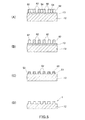
[インプリントモールド製造用の基板]
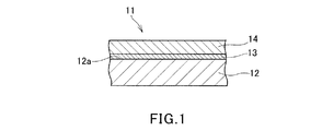
図1は、本発明のインプリントモールド製造用の基板の一実施形態を示す部分断面図である。図1において、インプリントモールド製造用の基板11は、基材12と、この基材の一の主面12a上に位置する基部ハードマスク材料層13と、この基部ハードマスク材料層13上に位置する芯材層14とを備えている。
基材12の材質は適宜選択することができるが、例えば、インプリントモールドをいわゆる光インプリント用のモールドとして使用する場合、基材12は照射光が透過可能な材質からなり、例えば、石英ガラス、珪酸系ガラス、フッ化カルシウム、フッ化マグネシウム、アクリルガラス等のガラスや、ポリカーボネート、ポリプロピレン、ポリエチレン等の樹脂等、あるいは、これらの任意の積層材を用いることができる。また、例えば、インプリントモールドをいわゆる熱インプリント用のモールドとして使用する場合、基材12は必ずしも透明基材である必要はなく、例えばニッケル、チタン、アルミニウムなどの金属、シリコンや窒化ガリウム等の半導体などを用いてもよい。このような基材12の厚さは、基材12の強度、取り扱い適性等を考慮して設定することができ、例えば、300μm〜10mm程度の範囲で適宜設定することができる。
[Substrates for imprint mold production]
FIG. 1 is a partial cross-sectional view showing an embodiment of a substrate for producing an imprint mold of the present invention. In FIG. 1, a
The material of the
インプリントモールド製造用の基板11を構成する基部ハードマスク材料層13は、基材12をエッチングする際に、基材12に比べてエッチングレートが小さく耐エッチング性を有する材料を用いることができ、基材12を考慮して適宜材料を選定することができる。例えば、クロム、チタン、タンタル、珪素、アルミニウム等の金属、窒化クロム、酸化クロム、酸窒化クロム等のクロム系化合物、酸化タンタル、酸窒化タンタル、酸化硼化タンタル、酸窒化硼化タンタル等のタンタル化合物、窒化チタン、窒化珪素、酸窒化珪素等を挙げることができ、これらのいずれかを単独で、あるいは、2種以上の組み合わせで使用することができる。また、基部ハードマスク材料層13は、2層以上の積層膜として構成してもよい。基部ハードマスク材料層13の厚さは、例えば、50nm以下、特に、1〜20nm、より好ましくは3〜10nm程度とすることができる。このような基部ハードマスク材料層13は、例えば、スパッタリング法、真空蒸着法、イオンプレーティング法等により形成することができる。
The base hard
インプリントモールド製造用の基板11を構成する芯材層14は、プラズマ化したフッ素系ガスを用いるエッチング、例えば、CF4、CHF3、C2F6等のフッ素系ガスをプラズマ化して行う反応性イオンエッチング等によりエッチングが可能なシリコン系材料からなる。このようなシリコン系材料としては、例えば、チタン(Ti)、バナジウム(V)、ニオブ(Nb)、モリブデン(Mo)、ジルコニウム(Zr)、ルテニウム(Ru)、ロジウム(Rh)、クロム(Cr)、ニッケル(Ni)、ハフニウム(Hf)、タンタル(Ta)等の遷移金属とシリコン(Si)との化合物を挙げることができる。芯材層14を構成するシリコン系材料に遷移金属が含有されることにより、後述するように芯材層14をエッチングして形成される芯材パターンは、電子線照射等による修正時のエッチングレートが速くなる。シリコン系材料における遷移金属の含有量は、下限値については1原子%以上であることが好ましい。特に、遷移金属とシリコンの原子比をATM/ASiとした場合、ATM/ASi>1/10の関係であると、電子線照射等による修正時のエッチングレートが速く、修正が容易となる。しかし、遷移金属の含有量が1原子%未満であると、電子線照射等による芯材パターンの修正に時間がかかり好ましくない。一方、シリコン系材料における遷移金属の含有量の上限値については50原子%以下が好ましい。遷移金属の含有量が50原子%を超えると、プラズマ化したフッ素系ガスを用いるエッチングが困難となり好ましくない。芯材層14の厚さは、例えば、10〜50nm、より好ましくは20〜40nm程度とすることができる。このような芯材層14は、例えば、スパッタリング法、真空蒸着法、イオンプレーティング法等により形成することができる。
The
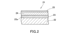
図2は、本発明のインプリントモールド製造用の基板の他の実施形態を示す部分断面図である。図2において、インプリントモールド製造用の基板21は、基材22と、この基材の一の主面22a上に位置する基部ハードマスク材料層23、この基部ハードマスク材料層23上に位置する芯材層24、この芯材層24上に位置する上部ハードマスク材料層25とを備えている。
インプリントモールド製造用の基板21を構成する基材22、基部ハードマスク材料層23および芯材層24は、上述のインプリントモールド製造用の基板11を構成する基材12、基部ハードマスク材料層13および芯材層14と同様であり、ここでの説明は省略する。
インプリントモールド製造用の基板21を構成する上部ハードマスク材料層25は、芯材層24をエッチングする際に、芯材層24に比べてエッチングレートが小さく耐エッチング性を有する材料を用いることができ、基部ハードマスク材料層13の説明で挙げた材料等から、芯材層24を考慮して適宜を選定することができる。
FIG. 2 is a partial cross-sectional view showing another embodiment of a substrate for producing an imprint mold of the present invention. In FIG. 2, a
The
For the upper hard
ここで、基部ハードマスク材料層23と上部ハードマスク材料層25は、インプリントモールド製造用の基板21を用いた後述のインプリントモールドの製造方法において、上部ハードマスク材料層25から形成する上部ハードマスクを除去する際に、基部ハードマスク材料層23が所望の厚みで残るように設定される。例えば、塩素系ガスと酸素との混合ガスを用いた反応性イオンエッチングに対する上部ハードマスク材料層25のエッチング耐性が、基部ハードマスク材料層23のエッチング耐性よりも低いものとする。また、基部ハードマスク材料層23と上部ハードマスク材料層25が同じ材料で構成されている場合、上部ハードマスク材料層25の厚さを、基部ハードマスク材料層23の厚さよりも薄いものとする。尚、塩素系ガスと酸素との混合ガスを用いた反応性イオンエッチングに対する上部ハードマスク材料層25のエッチング耐性が、基部ハードマスク材料層23のエッチング耐性よりも低い場合でも、上部ハードマスク材料層25の厚さを、基部ハードマスク材料層23の厚さより薄くしてもよい。
Here, the base hard
また、上部ハードマスク材料層25は、その光反射率が、基部ハードマスク材料層23の光反射率よりも高くなるようにしてもよい。これにより、後述するインプリントモールドの製造方法の検査・修正工程における光学的検査において、上部ハードマスク材料層25において反射された検査光の光量と、基部ハードマスク材料層23において反射された検査光の光量との差が大きくなり、検査精度が高いものとなる。また、逆に、上部ハードマスク材料層25の光反射率を、基部ハードマスク材料層23の光反射率よりも低くなるようにして、上部ハードマスク材料層25において反射された検査光の光量よりも、基部ハードマスク材料層23において反射された検査光の光量を大きくしてもよい。
上部ハードマスク材料層25の厚さは、塩素系ガスと酸素との混合ガスを用いた反応性イオンエッチングに対するエッチング耐性、基部ハードマスク材料層23の厚さ等を考慮して設定することができ、例えば、1〜10nm、より好ましくは2〜5nm程度とすることができる。このような上部ハードマスク材料層25は、スパッタリング法、真空蒸着法、イオンプレーティング法等により形成することができる。
Further, the upper hard
The thickness of the upper hard
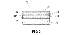
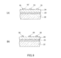
図3は、本発明のインプリントモールド製造用の基板の他の実施形態を示す部分断面図である。図3において、インプリントモールド製造用の基板31は、基材32と、この基材の一の主面32a上に位置する基部ハードマスク材料層33、この基部ハードマスク材料層33上に位置する芯材層34、この芯材層34上に位置する上部ハードマスク材料層35とを備え、芯材層34が2層構造である点を除いて、上述のインプリントモールド製造用の基板21と同じである。このため、基材32、基部ハードマスク材料層33、上部ハードマスク材料層35の説明は省略する。
FIG. 3 is a partial cross-sectional view showing another embodiment of a substrate for producing an imprint mold of the present invention. In FIG. 3, a
インプリントモールド製造用の基板31を構成する2層構造の芯材層34は、プラズマ化したフッ素系ガスを用いるエッチング、例えば、CF4、CHF3、C2F6等のフッ素系ガスをプラズマ化して行う反応性イオンエッチング等によりエッチングが可能なシリコン系材料からなる。例えば、この芯材層34を構成する2層のうち、基部ハードマスク材料層33側に位置する構成層34Aは酸化シリコンを含有し、上部ハードマスク材料層35側に位置する構成層34Bは遷移金属とシリコンを含有するものであってよい。構成層34Aは、後述するように芯材層34をエッチングして芯材パターンを形成する際に、基部ハードマスク材料層33に対して垂直性のよいエッチングを可能とするものであり、厚さは、例えば、5〜40nm、より好ましくは10〜30nm程度とすることができる。また、構成層34Bは、上述の芯材層14,24と同様とすることができ、厚さは、例えば、5〜40nm、より好ましくは10〜30nm程度とすることができる。このような2層構造の芯材層34の厚さは、例えば、10〜80nm、より好ましくは20〜50nm程度とすることができる。この芯材層34は、例えば、スパッタリング法、真空蒸着法、イオンプレーティング法等により形成することができる。
The
このようなインプリントモールド製造用の基板11,21,31は、芯材層14,24,34がシリコン系材料からなるので、インプリントモールドの製造時に、芯材層14,24,34をエッチングして形成される芯材パターンに欠陥等が存在する場合、欠陥箇所の除去や、欠陥箇所の補充修復を行うことができ、精度の高いインプリントモールドの製造を可能とする。
上述のインプリントモールド製造用の基板の実施形態は例示であり、本発明はこれらの実施形態に限定されるものではない。例えば、インプリントモールド製造用の基板11を構成する芯材層14が、芯材層34のような2層構造であってもよい。
In such an imprint
The above-described embodiments of the substrate for imprint mold production are examples, and the present invention is not limited to these embodiments. For example, the
[インプリントモールドの製造方法]
図4および図5は、本発明のインプリントモールドの製造方法の一実施形態を説明するための工程図である。この実施形態では、上述の本発明のインプリントモールド製造用の基板11を使用した例としている。上述のように、インプリントモールド製造用の基板11は、プラズマ化したフッ素系ガスを用いるエッチングが可能なシリコン系材料で芯材層14が形成されたものである。
本発明のインプリントモールドの製造方法では、レジストパターン形成工程において、インプリントモールド製造用の基板11の芯材層14上に、レジストパターン51を形成する(図4(A))。尚、図4(A)では、レジストパターンの一部に不要なレジストが存在する欠陥箇所51′が発生している例としており、欠陥箇所51′を鎖線で示している。この欠陥箇所51′に起因する欠陥は、後述する検査・修正工程にて解消することができる。
レジストパターン51は、例えば、電子線感応型のレジストを使用した電子線(EB)リソグラフィ法、感光性レジストを使用したフォトリソグラフィ法、インプリント法により形成することができる。
尚、本実施形態では、レジストパターン形成工程において、形成したレジストパターン51に対して酸素プラズマ処理等を施して、所望の寸法まで縮小するスリミングを行ってもよい。
[Imprint Mold Manufacturing Method]
4 and 5 are process diagrams for explaining an embodiment of the method for producing an imprint mold of the present invention. In this embodiment, the above-described
In the imprint mold manufacturing method of the present invention, in the resist pattern forming step, a resist
The resist
In the present embodiment, in the resist pattern forming step, slimming may be performed to reduce the dimensions to a desired dimension by performing oxygen plasma treatment or the like on the formed resist
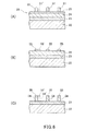
次に、芯材パターン形成工程において、レジストパターン51をエッチングマスクとして、芯材層14をエッチングして、基部ハードマスク材料層13上に芯材パターン54を形成する(図4(B))。芯材層14のエッチングは、CF4、CHF3、C2F6等のフッ素系ガスをプラズマ化して行う反応性イオンエッチング等により実施することができる。この芯材パターン54の形成では、上記のレジストパターン51の欠陥箇所51′に対応した芯材パターンの欠陥箇所54′(図4(B)では、鎖線で示している)が発生する。
尚、本実施形態では、芯材パターン形成工程において、形成した芯材パターン54に対してウエットエッチング処理等を施して、所望の寸法まで縮小するスリミングを行ってもよい。
次いで、検査・修正工程において、芯材パターン54を検査し、必要に応じて修正する。芯材パターン54の検査は、光学顕微鏡、電子顕微鏡等を用いた公知の検査手段により、芯材パターン54の寸法、形状を計測、観察する。この検査では、上記の芯材パターンの欠陥箇所54′が検出される。本発明では、芯材層14がシリコン系材料からなる基板を使用するので、形成された芯材パターン54は、電子線照射等により不要箇所を除去する修正が可能であり、また、欠損箇所にシリコン系材料を補充し、さらに必要に応じて電子線照射により所望の寸法、形状とする修正が可能である。図示例では、欠陥箇所54′は不要な部位が存在する欠陥であり、この欠陥箇所54′が検出された後、これを電子線照射により除去することにより、欠陥箇所のない芯材パターン54が得られる(図4(C))。
Next, in the core material pattern forming step, the
In the present embodiment, in the core material pattern forming step, the formed
Next, in the inspection / correction process, the
次に、側壁材料膜形成工程において、芯材パターン54を被覆するように側壁材料膜61を形成する(図4(D))。側壁材料膜61は、例えば、プラズマ化したフッ素系ガスを用いるエッチングに対してエッチング耐性を有し、かつ、プラズマ化した塩素系ガスを用いるエッチングによりエッチングが可能な材料で形成することができる。このような材料としては、例えば、酸化アルミニウム、タンタル化合物、タンタルと窒素とを含む化合物、タンタルとホウ素とを含み更に酸素と窒素の少なくとも一方を含む化合物、タンタルとシリコンとを含む化合物、タンタルとシリコンと窒素とを含む化合物、タンタルとゲルマニウムとを含む化合物、タンタルとゲルマニウムと窒素とを含む化合物等を挙げることができる。側壁材料膜61の形成は、所望の厚さで成膜が可能な公知の手段により行うことができ、例えば、ALD法(原子層堆積法)、真空成膜法等により側壁材料膜61を形成することができる。特に、ALD法では、所定の厚さが得られるまで、一連の原子層が連続的に積み重ねられ、被着させる面が凹凸面、湾曲面等であっても均一な成膜が可能である。側壁材料膜61の厚さは、後述するように形成する側壁パターンに要求される厚さに応じて設定することができ、例えば、数nm〜50nmの範囲で適宜設定することができる。
Next, in the side wall material film forming step, a side
次いで、エッチバック工程において、側壁材料膜61をエッチバックして、芯材パターン54の上面と基部ハードマスク材料層13とを露出させるとともに、側壁材料膜61を芯材パターン54の側壁に残して、側壁材料膜からなる側壁パターン62を形成する(図5(A))。エッチバックとは、エッチングにより表面を全体的に厚さ方向に削っていく操作であり、芯材パターン54の上面と基部ハードマスク材料層13とを確実に露出させることができるようにオーバーエッチングしてもよい。上述のように、側壁材料膜61は、プラズマ化した塩素系ガスを用いるエッチングによりエッチングが可能な材料で形成されている。したがって、側壁材料膜61のエッチバックは、塩素系ガスをプラズマ化して行う反応性イオンエッチング等により実施することができる。
次に、芯材パターン除去工程において、側壁パターン62間に位置する芯材パターン54を除去する(図5(B))。芯材パターン54は、フッ素系ガスをプラズマ化して行う反応性イオンエッチング等により除去することができる。上述のように、側壁材料膜61はプラズマ化したフッ素系ガスを用いるエッチングに対してエッチング耐性を具備しているので、この芯材パターン54の除去では、側壁パターン62にダメージを与えることなく芯材パターン54を除去することができる。
Next, in the etch back process, the
Next, in the core material pattern removing step, the
次に、基材エッチング工程において、側壁パターン62をエッチングマスクとして基部ハードマスク材料層13をエッチングしてハードマスク53を形成し(図5(C))、さらに、このハードマスク53をエッチングマスクとして基材12をエッチングし、その後、残存する側壁パターン62とハードマスク53を除去する(図5(D))。これにより、所望の凹凸構造を有するインプリントモールド1を作製することができる。ハードマスク材料層13のエッチングは、塩素系ガスと酸素の混合ガスをプラズマ化して行う反応性イオンエッチング等により実施することができる。また、基材12をエッチングするためのエッチングガスは、基材12とハードマスク53の材質を考慮して適宜選定することができる。例えば、基材12の材質が石英であり、ハードマスク53の材質がクロムである場合、エッチングガスを四フッ化炭素(CF4)等のフッ素系ガスとすることが好ましい。
図6、図7および図8は、本発明のインプリントモールドの製造方法の他の実施形態を説明するための工程図である。この実施形態では、上述の本発明のインプリントモールド製造用の基板21を使用した例としている。上述のように、インプリントモールド製造用の基板21では、芯材層24は、プラズマ化したフッ素系ガスを用いるエッチングが可能なシリコン系材料で形成されている。
Next, in the base material etching step, the base hard
6, 7 and 8 are process diagrams for explaining another embodiment of the method for producing an imprint mold of the present invention. In this embodiment, the above-described
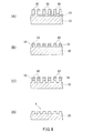
本発明のインプリントモールドの製造方法では、レジストパターン形成工程において、インプリントモールド製造用の基板21の上部ハードマスク材料層25上に、レジストパターン51を形成する(図6(A))。尚、図6(A)では、レジストパターンの一部に不要なレジストが存在する欠陥箇所51′が発生している例としており、欠陥箇所51′を鎖線で示している。この欠陥箇所51′に起因する欠陥は、後述する検査・修正工程にて解消することができる。
レジストパターン51の形成は、上述のインプリントモールドの製造方法と同様とすることができる。また、本実施形態においても、レジストパターン形成工程において、形成したレジストパターン51に対して酸素プラズマ処理等を施して、所望の寸法まで縮小するスリミングを行ってもよい。
In the imprint mold manufacturing method of the present invention, in the resist pattern forming step, a resist
The formation of the resist
次に、上部ハードマスク形成工程において、レジストパターン51をエッチングマスクとして、上部ハードマスク材料層25をエッチングして上部ハードマスク55を形成する(図6(B))。上部ハードマスク材料層25のエッチングは、塩素系ガスと酸素の混合ガスをプラズマ化して行う反応性イオンエッチング等により実施することができる。この上部ハードマスク55の形成では、上記のレジストパターン51の欠陥箇所51′に対応した上部ハードマスク55の欠陥箇所55′(図6(B)では、鎖線で示している)が発生する。
次に、芯材パターン形成工程において、上部ハードマスク55をエッチングマスクとして、芯材層24をエッチングして、基部ハードマスク材料層23上に芯材パターン54を形成する(図6(C))。芯材層24のエッチングは、CF4、CHF3、C2F6等のフッ素系ガスをプラズマ化して行う反応性イオンエッチング等により実施することができる。図6(C)では、上記の上部ハードマスク55の欠陥箇所55′に対応した芯材パターンの欠陥箇所54′(図6(B)では、鎖線で示している)が発生している。
Next, in the upper hard mask forming step, the upper hard
Next, in the core material pattern forming step, the
本実施形態では、この芯材パターン形成工程と、後述する側壁材料膜形成工程との間に、検査・修正工程を有している。この検査・修正工程では、形成された芯材パターン54を検査し、必要に応じて修正する。芯材パターン54の検査では、芯材パターン54上に残存する上部ハードマスク55の寸法、形状を、光学顕微鏡、電子顕微鏡等を用いた公知の検査手段により計測、観察する。この検査により、上記の上部ハードマスク55の欠陥箇所55′、芯材パターンの欠陥箇所54′が検出される。尚、上述のように、インプリントモールド製造用の基板21は、上部ハードマスク材料層25の光反射率が、基部ハードマスク材料層23の光反射率よりも高くなるようにしてもよく、このような態様である場合、形成された上部ハードマスク55において反射された検査光の光量と、基部ハードマスク材料層23において反射された検査光の光量との差が大きくなり、検査精度が高いものとなる。また、インプリントモールド製造用の基板21は、上部ハードマスク材料層25の光反射率を、基部ハードマスク材料層23の光反射率よりも低くなるようにして、上部ハードマスク55において反射された検査光の光量よりも、基部ハードマスク材料層23において反射された検査光の光量を大きくしてもよい。
In the present embodiment, an inspection / correction process is provided between the core material pattern forming process and a side wall material film forming process described later. In this inspection / correction process, the formed
検出された芯材パターンの欠陥箇所54′の修正は、例えば、検出された上部ハードマスク55の欠陥箇所55′を電子線照射等により除去し、その後、芯材パターンの欠陥箇所54′を電子線照射により除去することにより行うことができ、これにより、欠陥箇所のない芯材パターン54が得られる(図7(A))。本発明では、芯材層24がシリコン系材料からなる基板を使用するので、形成された芯材パターン54は、電子線照射等により不要箇所を除去する修正が可能であり、また、欠損箇所にシリコン系材料を補充し、さらに必要に応じて電子線照射により所望の寸法、形状とする修正が可能である。
尚、本実施形態では、芯材パターン形成工程において、形成した芯材パターン54に対してウエットエッチング処理等を施して、所望の寸法まで縮小するスリミングを行ってもよい。
次に、側壁材料膜形成工程において、芯材パターン54上に残存する上部ハードマスク55を、塩素系ガスと酸素の混合ガスをプラズマ化して行う反応性イオンエッチング等により除去(図7(B))した後、芯材パターン54を被覆するように側壁材料膜61を形成する(図7(C))。側壁材料膜61は、上述のインプリントモールドの製造方法における側壁材料膜61の形成と同様にして、形成することができる。
For the correction of the detected defect 54 'of the core material pattern, for example, the detected defect 55' of the upper
In the present embodiment, in the core material pattern forming step, the formed
Next, in the side wall material film formation step, the upper
上述のように、基板21では、塩素系ガスと酸素との混合ガスを用いた反応性イオンエッチングで上部ハードマスク55を除去したときに、基部ハードマスク材料層23は所望の厚さを維持するので、後工程において、この基部ハードマスク材料層23から形成するハードマスク53は、基材21を所望の深さまでエッチングする際のエッチングマスクとして機能することができる。
次いで、エッチバック工程において、側壁材料膜61をエッチバックして、芯材パターン54の上面と基部ハードマスク材料層23とを露出させるとともに、側壁材料膜61を芯材パターン54の側壁に残して、側壁材料膜からなる側壁パターン62を形成する(図7(D))。側壁材料膜61のエッチバックは、塩素系ガスをプラズマ化して行う反応性イオンエッチング等により実施することができる。
次に、芯材パターン除去工程において、側壁パターン62間に位置する芯材パターン54を除去する(図8(A))。芯材パターン54は、フッ素系ガスをプラズマ化して行う反応性イオンエッチング等により除去することができる。側壁材料膜61はプラズマ化したフッ素系ガスを用いるエッチングに対してエッチング耐性を具備しているので、この芯材パターン54の除去では、側壁パターン62にダメージを与えることなく芯材パターン54を除去することができる。
As described above, in the
Next, in the etch back process, the
Next, in the core material pattern removing step, the
次に、基材エッチング工程において、側壁パターン62をエッチングマスクとして基部ハードマスク材料層23をエッチングしてハードマスク53を形成し(図8(B))、さらに、このハードマスク53をエッチングマスクとして基材22をエッチングし(図8(C))、残存する側壁パターン62、ハードマスク53を除去する(図8(D))。これにより、所望の凹凸構造を有するインプリントモールド1を作製することができる。ハードマスク材料層23のエッチングは、塩素系ガスと酸素の混合ガスをプラズマ化して行う反応性イオンエッチング等により実施することができる。また、基材22をエッチングするためのエッチングガスは、基材22とハードマスク53の材質を考慮して適宜選定することができる。例えば、基材22の材質が石英であり、ハードマスク53の材質がクロムである場合、エッチングガスを四フッ化炭素(CF4)等のフッ素系ガスとすることが好ましい。
Next, in the base material etching step, the base hard
本実施形態では、芯材パターン形成工程と側壁材料膜形成工程との間に検査・修正工程を有することに代えて、上部ハードマスク形成工程と芯材パターン形成工程との間に検査・修正工程を有するものとしてもよい。この検査・修正工程では、上部ハードマスク形成工程において形成された上部ハードマスク55(図9(A))を検査し、必要に応じて修正する。上部ハードマスク55の検査は、光学顕微鏡、電子顕微鏡等を用いた公知の検査手段により、上部ハードマスク55の寸法、形状を計測、観察する。また、上述のように、インプリントモールド製造用の基板21は、上部ハードマスク材料層25の光反射率が、基部ハードマスク材料層23の光反射率よりも高くなるようにしてもよく、このような態様である場合、形成された上部ハードマスク55において反射された検査光の光量と、基部ハードマスク材料層23において反射された検査光の光量との差が大きくなり、検査精度が高いものとなる。また、インプリントモールド製造用の基板21は、上部ハードマスク材料層25の光反射率を、基部ハードマスク材料層23の光反射率よりも低くなるようにして、上部ハードマスク55において反射された検査光の光量よりも、基部ハードマスク材料層23において反射された検査光の光量を大きくしてもよい。
In this embodiment, instead of having an inspection / correction step between the core material pattern formation step and the sidewall material film formation step, an inspection / correction step between the upper hard mask formation step and the core material pattern formation step It is good also as what has. In this inspection / correction step, the upper hard mask 55 (FIG. 9A) formed in the upper hard mask formation step is inspected and corrected as necessary. The upper
このような検査によって、上部ハードマスク55の欠陥箇所55′が検出される。検出された上部ハードマスク55の欠陥箇所55′は、電子線照射等により除去して修正することができる(図9(B))。また、上部ハードマスク55の欠陥箇所55′が、上部ハードマスク55の欠損部位である場合、欠損部位にハードマスク材料を補充し、さらに必要に応じて電子線照射により所望の寸法、形状とする修正が可能である。
上述のインプリントモールドの製造方法の実施形態は例示であり、本発明はこれらの実施形態に限定されるものではない。例えば、インプリントモールド製造用の基板として、基板31を使用して、基板21を使用した場合と同様に、インプリントモールドを製造してもよい。この基板31の芯材層34の構成層34Aは、芯材層34をエッチングして芯材パターン54を形成する際に、基部ハードマスク材料層33に対して垂直性のよいエッチングが可能となり、より精度の高いインプリントモールドの製造が可能となる。
By such inspection, a
The above-described embodiments of the imprint mold manufacturing method are exemplifications, and the present invention is not limited to these embodiments. For example, an imprint mold may be manufactured using the
本発明は、微細加工に使用される種々のインプリントモールドの製造に適用することができる。 The present invention can be applied to the production of various imprint molds used for microfabrication.
11,21,31…インプリントモールド製造用の基板
12,22,32…基材
13,23,33…基部ハードマスク材料層
14,24,34…芯材層
25,35…上部ハードマスク材料層
51…レジストパターン
53…ハードマスク
54…芯材パターン
55…上部ハードマスク
61…側壁材料膜
62…側壁パターン
11, 21, 31 ... Substrate for
Claims (15)
前記芯材層は2層構造であり、該2層のうち前記基部ハードマスク材料層側に位置する層は酸化シリコンを含有し、他の層は遷移金属とシリコンとを含有することを特徴とするインプリントモールド製造用の基板。 A base material, a base hard mask material layer positioned on one main surface of the base material, and a core material layer positioned on the base hard mask material layer, wherein the core material layer is plasmatized fluorine gas Ri Do a silicon-based material that can be etched using,
The core material layer has a two-layer structure, and the layer located on the base hard mask material layer side of the two layers contains silicon oxide, and the other layers contain a transition metal and silicon. Substrate for imprint mold manufacturing.
前記芯材層は遷移金属を含有し、The core material layer contains a transition metal,
前記芯材層における前記遷移金属の含有量は、1原子%以上であることを特徴とするインプリントモールド製造用の基板。The substrate for imprint mold production, wherein the content of the transition metal in the core material layer is 1 atomic% or more.
前記レジストパターンをエッチングマスクとして、前記芯材層をエッチングして芯材パターンを形成する芯材パターン形成工程と、
前記芯材パターンを検査し、必要に応じて修正する検査・修正工程と、
前記芯材パターンを被覆するように側壁材料膜を形成する側壁材料膜形成工程と、
前記側壁材料膜をエッチバックして、前記芯材パターンの上面と前記基部ハードマスク材料層とを露出させるとともに、前記側壁材料膜を前記芯材パターンの側壁に残して、前記側壁材料膜からなる側壁パターンを形成するエッチバック工程と、
前記芯材パターンを除去する芯材パターン除去工程と、
前記側壁パターンをエッチングマスクとして前記基部ハードマスク材料層をエッチングしてハードマスクを形成し、該ハードマスクをエッチングマスクとして前記基材をエッチングする基材エッチング工程と、を有し、
前記芯材層は、プラズマ化したフッ素ガスを用いるエッチングが可能なシリコン系材料からなり、
前記芯材層は2層構造であり、該2層のうち前記基部ハードマスク材料層側に位置する層は酸化シリコンを含有し、他の層は遷移金属とシリコンとを含有することを特徴とするインプリントモールドの製造方法。 A resist pattern forming step of forming a resist pattern on the core material layer of the substrate for imprint mold production in which the base hard mask material layer and the core material layer are laminated in this order on one main surface of the base material When,
Using the resist pattern as an etching mask, a core material pattern forming step of forming the core material pattern by etching the core material layer;
Inspecting and correcting the core material pattern, and correcting as necessary,
A sidewall material film forming step of forming a sidewall material film so as to cover the core material pattern;
The sidewall material film is etched back to expose the upper surface of the core material pattern and the base hard mask material layer, and the sidewall material film is left on the sidewall of the core material pattern, and is made of the sidewall material film. An etch back step of forming a sidewall pattern;
A core material pattern removing step for removing the core material pattern;
Etching the base hard mask material layer using the sidewall pattern as an etching mask to form a hard mask, and etching the base material using the hard mask as an etching mask,
The core material layer is made of a silicon-based material that can be etched using plasmad fluorine gas ,
The core material layer has a two-layer structure, and the layer located on the base hard mask material layer side of the two layers contains silicon oxide, and the other layers contain a transition metal and silicon. A method for manufacturing an imprint mold.
前記レジストパターンをエッチングマスクとして、前記芯材層をエッチングして芯材パターンを形成する芯材パターン形成工程と、Using the resist pattern as an etching mask, a core material pattern forming step of forming the core material pattern by etching the core material layer;
前記芯材パターンを検査し、必要に応じて修正する検査・修正工程と、Inspecting and correcting the core material pattern, and correcting as necessary,
前記芯材パターンを被覆するように側壁材料膜を形成する側壁材料膜形成工程と、A sidewall material film forming step of forming a sidewall material film so as to cover the core material pattern;
前記側壁材料膜をエッチバックして、前記芯材パターンの上面と前記基部ハードマスク材料層とを露出させるとともに、前記側壁材料膜を前記芯材パターンの側壁に残して、前記側壁材料膜からなる側壁パターンを形成するエッチバック工程と、The sidewall material film is etched back to expose the upper surface of the core material pattern and the base hard mask material layer, and the sidewall material film is left on the sidewall of the core material pattern, and is made of the sidewall material film. An etch back step of forming a sidewall pattern;
前記芯材パターンを除去する芯材パターン除去工程と、A core material pattern removing step for removing the core material pattern;
前記側壁パターンをエッチングマスクとして前記基部ハードマスク材料層をエッチングしてハードマスクを形成し、該ハードマスクをエッチングマスクとして前記基材をエッチングする基材エッチング工程と、を有し、Etching the base hard mask material layer using the sidewall pattern as an etching mask to form a hard mask, and etching the base material using the hard mask as an etching mask,
前記芯材層は、プラズマ化したフッ素ガスを用いるエッチングが可能なシリコン系材料からなり、The core material layer is made of a silicon-based material that can be etched using plasmad fluorine gas,
前記芯材層は遷移金属を含有し、The core material layer contains a transition metal,
前記芯材層における前記遷移金属の含有量は、1原子%以上であることを特徴とするインプリントモールドの製造方法。Content of the said transition metal in the said core material layer is 1 atomic% or more, The manufacturing method of the imprint mold characterized by the above-mentioned.
前記レジストパターンをエッチングマスクとして、前記上部ハードマスク材料層をエッチングして上部ハードマスクを形成する上部ハードマスク形成工程と、
前記上部ハードマスクをエッチングマスクとして、前記芯材層をエッチングして芯材パターンを形成する芯材パターン形成工程と、
前記上部ハードマスクを除去した後、前記芯材パターンを被覆するように側壁材料膜を形成する側壁材料膜形成工程と、
前記側壁材料膜をエッチバックして、前記芯材パターンの上面と前記基部ハードマスク材料層とを露出させるとともに、前記側壁材料膜を前記芯材パターンの側壁に残して、前記側壁材料膜からなる側壁パターンを形成するエッチバック工程と、
前記芯材パターンを除去する芯材パターン除去工程と、
前記側壁パターンをエッチングマスクとして前記基部ハードマスク材料層をエッチングしてハードマスクを形成し、該ハードマスクをエッチングマスクとして前記基材をエッチングする基材エッチング工程と、を有し、
前記芯材層は、プラズマ化したフッ素ガスを用いるエッチングが可能なシリコン系材料からなり、
前記芯材層は2層構造であり、該2層のうち前記基部ハードマスク材料層側に位置する層は酸化シリコンを含有し、他の層は遷移金属とシリコンとを含有し、
前記上部ハードマスク形成工程と前記芯材パターン形成工程との間に、前記上部ハードマスク形成工程で形成した上部ハードマスクを検査し、必要に応じて修正する検査・修正工程を有する、または、前記芯材パターン形成工程と前記側壁材料膜形成工程との間に、前記芯材パターン形成工程で形成した芯材パターンを検査し、必要に応じて修正する検査・修正工程を有することを特徴とするインプリントモールドの製造方法。 A resist is formed on the upper hard mask material layer of the substrate for imprint mold production in which a base hard mask material layer, a core material layer, and an upper hard mask material layer are laminated in this order on one main surface of a base material. A resist pattern forming step for forming a pattern;
Using the resist pattern as an etching mask, an upper hard mask forming step of forming the upper hard mask by etching the upper hard mask material layer;
Using the upper hard mask as an etching mask, a core material pattern forming step for forming a core material pattern by etching the core material layer;
A sidewall material film forming step of forming a sidewall material film so as to cover the core material pattern after removing the upper hard mask;
The sidewall material film is etched back to expose the upper surface of the core material pattern and the base hard mask material layer, and the sidewall material film is left on the sidewall of the core material pattern, and is made of the sidewall material film. An etch back step of forming a sidewall pattern;
A core material pattern removing step for removing the core material pattern;
Etching the base hard mask material layer using the sidewall pattern as an etching mask to form a hard mask, and etching the base material using the hard mask as an etching mask,
The core material layer is made of a silicon-based material that can be etched using plasmad fluorine gas ,
The core material layer has a two-layer structure, and the layer located on the base hard mask material layer side of the two layers contains silicon oxide, and the other layers contain a transition metal and silicon,
Inspecting and correcting the upper hard mask formed in the upper hard mask forming step between the upper hard mask forming step and the core material pattern forming step, and correcting if necessary, or Between the core material pattern forming step and the sidewall material film forming step, the core material pattern formed in the core material pattern forming step is inspected, and has an inspection / correction step of correcting as necessary. Manufacturing method of imprint mold.
前記レジストパターンをエッチングマスクとして、前記上部ハードマスク材料層をエッチングして上部ハードマスクを形成する上部ハードマスク形成工程と、Using the resist pattern as an etching mask, an upper hard mask forming step of forming the upper hard mask by etching the upper hard mask material layer;
前記上部ハードマスクをエッチングマスクとして、前記芯材層をエッチングして芯材パターンを形成する芯材パターン形成工程と、Using the upper hard mask as an etching mask, a core material pattern forming step for forming a core material pattern by etching the core material layer;
前記上部ハードマスクを除去した後、前記芯材パターンを被覆するように側壁材料膜を形成する側壁材料膜形成工程と、A sidewall material film forming step of forming a sidewall material film so as to cover the core material pattern after removing the upper hard mask;
前記側壁材料膜をエッチバックして、前記芯材パターンの上面と前記基部ハードマスク材料層とを露出させるとともに、前記側壁材料膜を前記芯材パターンの側壁に残して、前記側壁材料膜からなる側壁パターンを形成するエッチバック工程と、The sidewall material film is etched back to expose the upper surface of the core material pattern and the base hard mask material layer, and the sidewall material film is left on the sidewall of the core material pattern, and is made of the sidewall material film. An etch back step of forming a sidewall pattern;
前記芯材パターンを除去する芯材パターン除去工程と、A core material pattern removing step for removing the core material pattern;
前記側壁パターンをエッチングマスクとして前記基部ハードマスク材料層をエッチングしてハードマスクを形成し、該ハードマスクをエッチングマスクとして前記基材をエッチングする基材エッチング工程と、を有し、Etching the base hard mask material layer using the sidewall pattern as an etching mask to form a hard mask, and etching the base material using the hard mask as an etching mask,
前記芯材層は、プラズマ化したフッ素ガスを用いるエッチングが可能なシリコン系材料からなり、The core material layer is made of a silicon-based material that can be etched using plasmad fluorine gas,
前記芯材層は遷移金属を含有し、The core material layer contains a transition metal,
前記芯材層における前記遷移金属の含有量は、1原子%以上であり、The content of the transition metal in the core material layer is 1 atomic% or more,
前記上部ハードマスク形成工程と前記芯材パターン形成工程との間に、前記上部ハードマスク形成工程で形成した上部ハードマスクを検査し、必要に応じて修正する検査・修正工程を有する、または、前記芯材パターン形成工程と前記側壁材料膜形成工程との間に、前記芯材パターン形成工程で形成した芯材パターンを検査し、必要に応じて修正する検査・修正工程を有することを特徴とするインプリントモールドの製造方法。Inspecting and correcting the upper hard mask formed in the upper hard mask forming step between the upper hard mask forming step and the core material pattern forming step, and correcting if necessary, or Between the core material pattern forming step and the sidewall material film forming step, the core material pattern formed in the core material pattern forming step is inspected, and has an inspection / correction step of correcting as necessary. Manufacturing method of imprint mold.
Priority Applications (1)
| Application Number | Priority Date | Filing Date | Title |
|---|---|---|---|
| JP2015144664A JP6565415B2 (en) | 2015-07-22 | 2015-07-22 | Substrate for imprint mold production and imprint mold production method |
Applications Claiming Priority (1)
| Application Number | Priority Date | Filing Date | Title |
|---|---|---|---|
| JP2015144664A JP6565415B2 (en) | 2015-07-22 | 2015-07-22 | Substrate for imprint mold production and imprint mold production method |
Publications (2)
| Publication Number | Publication Date |
|---|---|
| JP2017028081A JP2017028081A (en) | 2017-02-02 |
| JP6565415B2 true JP6565415B2 (en) | 2019-08-28 |
Family
ID=57946578
Family Applications (1)
| Application Number | Title | Priority Date | Filing Date |
|---|---|---|---|
| JP2015144664A Active JP6565415B2 (en) | 2015-07-22 | 2015-07-22 | Substrate for imprint mold production and imprint mold production method |
Country Status (1)
| Country | Link |
|---|---|
| JP (1) | JP6565415B2 (en) |
Families Citing this family (1)
| Publication number | Priority date | Publication date | Assignee | Title |
|---|---|---|---|---|
| JP2021048329A (en) | 2019-09-19 | 2021-03-25 | キオクシア株式会社 | Pattern formation method and template manufacturing method |
Family Cites Families (17)
| Publication number | Priority date | Publication date | Assignee | Title |
|---|---|---|---|---|
| JP2005044843A (en) * | 2003-07-23 | 2005-02-17 | Sii Nanotechnology Inc | Defect correction method of original plate for nanoimprint lithography |
| US8003310B2 (en) * | 2006-04-24 | 2011-08-23 | Micron Technology, Inc. | Masking techniques and templates for dense semiconductor fabrication |
| JP4996155B2 (en) * | 2006-07-18 | 2012-08-08 | 株式会社東芝 | Semiconductor device and manufacturing method thereof |
| JP4825891B2 (en) * | 2009-03-31 | 2011-11-30 | 株式会社東芝 | Semiconductor device manufacturing method and template |
| WO2010134176A1 (en) * | 2009-05-20 | 2010-11-25 | 株式会社 東芝 | Method for forming uneven pattern |
| EP2287667B1 (en) * | 2009-06-26 | 2013-03-27 | Rohm and Haas Electronic Materials, L.L.C. | Self-aligned spacer multiple patterning methods |
| JP2011023453A (en) * | 2009-07-14 | 2011-02-03 | Panasonic Corp | Method for manufacturing semiconductor device |
| JP2011258605A (en) * | 2010-06-04 | 2011-12-22 | Toshiba Corp | Patterning method and method of manufacturing semiconductor device |
| JP2012023109A (en) * | 2010-07-12 | 2012-02-02 | Toshiba Corp | Method for correcting defect of template, method for making template, and method for manufacturing semiconductor device |
| KR102056509B1 (en) * | 2012-07-13 | 2019-12-16 | 호야 가부시키가이샤 | Mask blank and method for manufacturing phase-shift mask |
| JP5962353B2 (en) * | 2012-09-06 | 2016-08-03 | 大日本印刷株式会社 | Method for producing template for nanoimprint lithography |
| JP6123242B2 (en) * | 2012-11-09 | 2017-05-10 | 大日本印刷株式会社 | Pattern formation method |
| JP6003571B2 (en) * | 2012-11-21 | 2016-10-05 | 大日本印刷株式会社 | Method for producing template for nanoimprint |
| JP6136721B2 (en) * | 2013-08-01 | 2017-05-31 | 大日本印刷株式会社 | Pattern forming method and imprint mold manufacturing method |
| JP6156013B2 (en) * | 2013-09-24 | 2017-07-05 | 大日本印刷株式会社 | Manufacturing method of imprint mold |
| JP6206667B2 (en) * | 2013-11-06 | 2017-10-04 | 大日本印刷株式会社 | Pattern formation method |
| JP6384040B2 (en) * | 2013-11-11 | 2018-09-05 | 大日本印刷株式会社 | Pattern forming method, imprint mold manufacturing method using the same, and imprint mold used therefor |
-
2015
- 2015-07-22 JP JP2015144664A patent/JP6565415B2/en active Active
Also Published As
| Publication number | Publication date |
|---|---|
| JP2017028081A (en) | 2017-02-02 |
Similar Documents
| Publication | Publication Date | Title |
|---|---|---|
| JP7201853B2 (en) | Mask blank, imprint mold manufacturing method, transfer mask manufacturing method, reflective mask manufacturing method, and semiconductor device manufacturing method | |
| JP5009649B2 (en) | Mask blank, exposure mask manufacturing method, reflective mask manufacturing method, and imprint template manufacturing method | |
| JP3683261B2 (en) | REFLECTIVE MASK BLANK HAVING FALSE DEFECT AND MANUFACTURING METHOD THEREOF, REFLECTIVE MASK HAVING FALSE DEFECT AND MANUFACTURING METHOD THEREOF | |
| KR100885636B1 (en) | Blank Mask and Manufacturing Method of Photomask Using the Same | |
| JP2015115461A (en) | Defect correction method and manufacturing method for microstructure | |
| CN102656516B (en) | The manufacture method of photomask blank and photomask | |
| JP6698438B2 (en) | Mask blank, transfer mask, mask blank manufacturing method, transfer mask manufacturing method, and semiconductor device manufacturing method | |
| CN109782527B (en) | Photomask blank and method for preparing photomask | |
| US20190302604A1 (en) | Mask blank, phase shift mask, method of manufacturing phase shift mask, and method of manufacturing semiconductor device | |
| JP2009206339A (en) | Mask blank for imprint molding and method for manufacturing imprint mold | |
| JP6127535B2 (en) | Method for producing template for nanoimprint | |
| JP5221168B2 (en) | Mask blank for imprint mold and method for producing imprint mold | |
| US20220035235A1 (en) | Mask blank, transfer mask, and semiconductor-device manufacturing method | |
| JP5673900B2 (en) | Manufacturing method of nanoimprint mold | |
| JP2011211083A (en) | Mask blanks, pattern forming method, and manufacturing method of mold | |
| TWI829823B (en) | Photomask blank substrate and photomask manufacturing method | |
| JP6236918B2 (en) | Method for producing template for nanoimprint | |
| JP6115245B2 (en) | Nanoimprint template and manufacturing method thereof | |
| JP6565415B2 (en) | Substrate for imprint mold production and imprint mold production method | |
| US11054735B2 (en) | Mask blank, phase shift mask, method for manufacturing phase shift mask, and method for manufacturing semiconductor device | |
| KR20080073824A (en) | Blank Stamps and Stamps for Nano Imprint Lithography | |
| JP2016092360A (en) | Defect correction method and method of manufacturing microstructure body | |
| JP6631271B2 (en) | Manufacturing method of imprint mold | |
| JP2021135370A (en) | Mask blank, production method for mold mask blank, and production method of imprint mold | |
| JP6206667B2 (en) | Pattern formation method |
Legal Events
| Date | Code | Title | Description |
|---|---|---|---|
| A621 | Written request for application examination |
Free format text: JAPANESE INTERMEDIATE CODE: A621 Effective date: 20180528 |
|
| A977 | Report on retrieval |
Free format text: JAPANESE INTERMEDIATE CODE: A971007 Effective date: 20190313 |
|
| A131 | Notification of reasons for refusal |
Free format text: JAPANESE INTERMEDIATE CODE: A131 Effective date: 20190319 |
|
| A521 | Request for written amendment filed |
Free format text: JAPANESE INTERMEDIATE CODE: A523 Effective date: 20190515 |
|
| TRDD | Decision of grant or rejection written | ||
| A01 | Written decision to grant a patent or to grant a registration (utility model) |
Free format text: JAPANESE INTERMEDIATE CODE: A01 Effective date: 20190702 |
|
| A61 | First payment of annual fees (during grant procedure) |
Free format text: JAPANESE INTERMEDIATE CODE: A61 Effective date: 20190715 |
|
| R150 | Certificate of patent or registration of utility model |
Ref document number: 6565415 Country of ref document: JP Free format text: JAPANESE INTERMEDIATE CODE: R150 |