JP6565082B2 - Coil topology for inductive power transfer - Google Patents
Coil topology for inductive power transfer Download PDFInfo
- Publication number
- JP6565082B2 JP6565082B2 JP2016538002A JP2016538002A JP6565082B2 JP 6565082 B2 JP6565082 B2 JP 6565082B2 JP 2016538002 A JP2016538002 A JP 2016538002A JP 2016538002 A JP2016538002 A JP 2016538002A JP 6565082 B2 JP6565082 B2 JP 6565082B2
- Authority
- JP
- Japan
- Prior art keywords
- coil
- magnetic flux
- layer
- flux device
- electric vehicle
- Prior art date
- Legal status (The legal status is an assumption and is not a legal conclusion. Google has not performed a legal analysis and makes no representation as to the accuracy of the status listed.)
- Active
Links
Images


Classifications
-
- H—ELECTRICITY
- H01—ELECTRIC ELEMENTS
- H01F—MAGNETS; INDUCTANCES; TRANSFORMERS; SELECTION OF MATERIALS FOR THEIR MAGNETIC PROPERTIES
- H01F38/00—Adaptations of transformers or inductances for specific applications or functions
- H01F38/14—Inductive couplings
-
- B—PERFORMING OPERATIONS; TRANSPORTING
- B60—VEHICLES IN GENERAL
- B60L—PROPULSION OF ELECTRICALLY-PROPELLED VEHICLES; SUPPLYING ELECTRIC POWER FOR AUXILIARY EQUIPMENT OF ELECTRICALLY-PROPELLED VEHICLES; ELECTRODYNAMIC BRAKE SYSTEMS FOR VEHICLES IN GENERAL; MAGNETIC SUSPENSION OR LEVITATION FOR VEHICLES; MONITORING OPERATING VARIABLES OF ELECTRICALLY-PROPELLED VEHICLES; ELECTRIC SAFETY DEVICES FOR ELECTRICALLY-PROPELLED VEHICLES
- B60L53/00—Methods of charging batteries, specially adapted for electric vehicles; Charging stations or on-board charging equipment therefor; Exchange of energy storage elements in electric vehicles
- B60L53/10—Methods of charging batteries, specially adapted for electric vehicles; Charging stations or on-board charging equipment therefor; Exchange of energy storage elements in electric vehicles characterised by the energy transfer between the charging station and the vehicle
- B60L53/12—Inductive energy transfer
- B60L53/122—Circuits or methods for driving the primary coil, e.g. supplying electric power to the coil
-
- H—ELECTRICITY
- H02—GENERATION; CONVERSION OR DISTRIBUTION OF ELECTRIC POWER
- H02J—CIRCUIT ARRANGEMENTS OR SYSTEMS FOR SUPPLYING OR DISTRIBUTING ELECTRIC POWER; SYSTEMS FOR STORING ELECTRIC ENERGY
- H02J50/00—Circuit arrangements or systems for wireless supply or distribution of electric power
- H02J50/10—Circuit arrangements or systems for wireless supply or distribution of electric power using inductive coupling
- H02J50/12—Circuit arrangements or systems for wireless supply or distribution of electric power using inductive coupling of the resonant type
-
- H—ELECTRICITY
- H02—GENERATION; CONVERSION OR DISTRIBUTION OF ELECTRIC POWER
- H02J—CIRCUIT ARRANGEMENTS OR SYSTEMS FOR SUPPLYING OR DISTRIBUTING ELECTRIC POWER; SYSTEMS FOR STORING ELECTRIC ENERGY
- H02J50/00—Circuit arrangements or systems for wireless supply or distribution of electric power
- H02J50/40—Circuit arrangements or systems for wireless supply or distribution of electric power using two or more transmitting or receiving devices
-
- H—ELECTRICITY
- H02—GENERATION; CONVERSION OR DISTRIBUTION OF ELECTRIC POWER
- H02J—CIRCUIT ARRANGEMENTS OR SYSTEMS FOR SUPPLYING OR DISTRIBUTING ELECTRIC POWER; SYSTEMS FOR STORING ELECTRIC ENERGY
- H02J50/00—Circuit arrangements or systems for wireless supply or distribution of electric power
- H02J50/60—Circuit arrangements or systems for wireless supply or distribution of electric power responsive to the presence of foreign objects, e.g. detection of living beings
-
- H—ELECTRICITY
- H02—GENERATION; CONVERSION OR DISTRIBUTION OF ELECTRIC POWER
- H02J—CIRCUIT ARRANGEMENTS OR SYSTEMS FOR SUPPLYING OR DISTRIBUTING ELECTRIC POWER; SYSTEMS FOR STORING ELECTRIC ENERGY
- H02J50/00—Circuit arrangements or systems for wireless supply or distribution of electric power
- H02J50/70—Circuit arrangements or systems for wireless supply or distribution of electric power involving the reduction of electric, magnetic or electromagnetic leakage fields
-
- H—ELECTRICITY
- H02—GENERATION; CONVERSION OR DISTRIBUTION OF ELECTRIC POWER
- H02J—CIRCUIT ARRANGEMENTS OR SYSTEMS FOR SUPPLYING OR DISTRIBUTING ELECTRIC POWER; SYSTEMS FOR STORING ELECTRIC ENERGY
- H02J50/00—Circuit arrangements or systems for wireless supply or distribution of electric power
- H02J50/80—Circuit arrangements or systems for wireless supply or distribution of electric power involving the exchange of data, concerning supply or distribution of electric power, between transmitting devices and receiving devices
-
- H—ELECTRICITY
- H02—GENERATION; CONVERSION OR DISTRIBUTION OF ELECTRIC POWER
- H02J—CIRCUIT ARRANGEMENTS OR SYSTEMS FOR SUPPLYING OR DISTRIBUTING ELECTRIC POWER; SYSTEMS FOR STORING ELECTRIC ENERGY
- H02J50/00—Circuit arrangements or systems for wireless supply or distribution of electric power
- H02J50/90—Circuit arrangements or systems for wireless supply or distribution of electric power involving detection or optimisation of position, e.g. alignment
-
- H—ELECTRICITY
- H02—GENERATION; CONVERSION OR DISTRIBUTION OF ELECTRIC POWER
- H02J—CIRCUIT ARRANGEMENTS OR SYSTEMS FOR SUPPLYING OR DISTRIBUTING ELECTRIC POWER; SYSTEMS FOR STORING ELECTRIC ENERGY
- H02J7/00—Circuit arrangements for charging or depolarising batteries or for supplying loads from batteries
- H02J7/00032—Circuit arrangements for charging or depolarising batteries or for supplying loads from batteries characterised by data exchange
- H02J7/00034—Charger exchanging data with an electronic device, i.e. telephone, whose internal battery is under charge
-
- Y—GENERAL TAGGING OF NEW TECHNOLOGICAL DEVELOPMENTS; GENERAL TAGGING OF CROSS-SECTIONAL TECHNOLOGIES SPANNING OVER SEVERAL SECTIONS OF THE IPC; TECHNICAL SUBJECTS COVERED BY FORMER USPC CROSS-REFERENCE ART COLLECTIONS [XRACs] AND DIGESTS
- Y02—TECHNOLOGIES OR APPLICATIONS FOR MITIGATION OR ADAPTATION AGAINST CLIMATE CHANGE
- Y02T—CLIMATE CHANGE MITIGATION TECHNOLOGIES RELATED TO TRANSPORTATION
- Y02T10/00—Road transport of goods or passengers
- Y02T10/60—Other road transportation technologies with climate change mitigation effect
- Y02T10/70—Energy storage systems for electromobility, e.g. batteries
-
- Y—GENERAL TAGGING OF NEW TECHNOLOGICAL DEVELOPMENTS; GENERAL TAGGING OF CROSS-SECTIONAL TECHNOLOGIES SPANNING OVER SEVERAL SECTIONS OF THE IPC; TECHNICAL SUBJECTS COVERED BY FORMER USPC CROSS-REFERENCE ART COLLECTIONS [XRACs] AND DIGESTS
- Y02—TECHNOLOGIES OR APPLICATIONS FOR MITIGATION OR ADAPTATION AGAINST CLIMATE CHANGE
- Y02T—CLIMATE CHANGE MITIGATION TECHNOLOGIES RELATED TO TRANSPORTATION
- Y02T10/00—Road transport of goods or passengers
- Y02T10/60—Other road transportation technologies with climate change mitigation effect
- Y02T10/7072—Electromobility specific charging systems or methods for batteries, ultracapacitors, supercapacitors or double-layer capacitors
-
- Y—GENERAL TAGGING OF NEW TECHNOLOGICAL DEVELOPMENTS; GENERAL TAGGING OF CROSS-SECTIONAL TECHNOLOGIES SPANNING OVER SEVERAL SECTIONS OF THE IPC; TECHNICAL SUBJECTS COVERED BY FORMER USPC CROSS-REFERENCE ART COLLECTIONS [XRACs] AND DIGESTS
- Y02—TECHNOLOGIES OR APPLICATIONS FOR MITIGATION OR ADAPTATION AGAINST CLIMATE CHANGE
- Y02T—CLIMATE CHANGE MITIGATION TECHNOLOGIES RELATED TO TRANSPORTATION
- Y02T90/00—Enabling technologies or technologies with a potential or indirect contribution to GHG emissions mitigation
- Y02T90/10—Technologies relating to charging of electric vehicles
- Y02T90/12—Electric charging stations
-
- Y—GENERAL TAGGING OF NEW TECHNOLOGICAL DEVELOPMENTS; GENERAL TAGGING OF CROSS-SECTIONAL TECHNOLOGIES SPANNING OVER SEVERAL SECTIONS OF THE IPC; TECHNICAL SUBJECTS COVERED BY FORMER USPC CROSS-REFERENCE ART COLLECTIONS [XRACs] AND DIGESTS
- Y02—TECHNOLOGIES OR APPLICATIONS FOR MITIGATION OR ADAPTATION AGAINST CLIMATE CHANGE
- Y02T—CLIMATE CHANGE MITIGATION TECHNOLOGIES RELATED TO TRANSPORTATION
- Y02T90/00—Enabling technologies or technologies with a potential or indirect contribution to GHG emissions mitigation
- Y02T90/10—Technologies relating to charging of electric vehicles
- Y02T90/14—Plug-in electric vehicles
Description
本開示は、一般にワイヤレス電力伝達に関し、より詳細には、電気車両などの遠隔システムへのワイヤレス電力伝達、ならびに結合器コイルトポロジーに関係するデバイス、システム、および方法に関する。 The present disclosure relates generally to wireless power transfer and, more particularly, to devices, systems, and methods related to wireless power transfer to remote systems, such as electric vehicles, and coupler coil topologies.
バッテリーなどのエネルギー蓄積デバイスから受信された電気から導出された運動力を含む、車両などのリモートシステムが導入されている。たとえば、ハイブリッド電気車両は、車両を充電するために、車両のブレーキおよび従来型モータからの電力を使用するオンボード充電器を含む。電気のみの車両は、一般に、他の供給源からバッテリーを充電するための電気を受信する。バッテリー式電気車両(電気車両)は、家庭用または商用の交流(AC)供給源などの何らかのタイプの有線ACを通して充電されるように提案されることが多い。有線充電接続は、電源に物理的に接続されているケーブルまたは他の同様のコネクタを必要とする。ケーブルおよび同様のコネクタは、時々不便であるか、または扱いにくく、かつ他の欠点を有する場合がある。電気車両を充電するために使用されるように(たとえば、ワイヤレス場を介して)自由空間内で電力を伝達することが可能なワイヤレス充電システムは、有線充電ソリューションの欠点の一部を克服することができる。したがって、ワイヤレス充電システムおよび方法は、電動車両を充電するための、電力を効率的かつ安全に伝達する。 Remote systems such as vehicles have been introduced that include athletic forces derived from electricity received from energy storage devices such as batteries. For example, a hybrid electric vehicle includes an on-board charger that uses power from the vehicle's brakes and conventional motors to charge the vehicle. Electric-only vehicles generally receive electricity to charge the battery from other sources. Battery powered electric vehicles (electric vehicles) are often proposed to be charged through some type of wired AC, such as a home or commercial alternating current (AC) source. Wired charging connections require a cable or other similar connector that is physically connected to the power source. Cables and similar connectors are sometimes inconvenient or cumbersome and may have other drawbacks. A wireless charging system capable of transferring power in free space to be used to charge an electric vehicle (eg, via a wireless field) overcomes some of the shortcomings of wired charging solutions Can do. Thus, the wireless charging system and method efficiently and safely transfers power to charge an electric vehicle.
添付の特許請求の範囲内のシステム、方法、およびデバイスの様々な実装形態は各々、いくつかの態様を有し、そのいずれの態様も単独では、本明細書で説明する望ましい属性に関与することはない。添付の特許請求の範囲を限定することなく、本明細書においていくつかの顕著な特徴について説明する。 Each of the various implementations of systems, methods, and devices within the scope of the appended claims has a number of aspects, each of which alone contributes to the desired attributes described herein. There is no. Without limiting the scope of the appended claims, some salient features are described herein.
本明細書で説明する主題の1つまたは複数の実装形態の詳細について、添付の図面および以下の説明において述べる。他の特徴、態様、および利点は、説明、図面、および特許請求の範囲から明らかになるであろう。以下の図の相対的な寸法は、一定の縮尺で描かれていない可能性があることに留意されたい。 The details of one or more implementations of the subject matter described in this specification are set forth in the accompanying drawings and the description below. Other features, aspects, and advantages will be apparent from the description, drawings, and claims. Note that the relative dimensions in the following figures may not be drawn to scale.
本開示の一態様は、磁束デバイスの上方のスペースとの間で磁束を送信または受信するように構成された磁束デバイスを提供する。本磁束デバイスは、少なくとも第1の導電性コイルと第2の導電性コイルとを備える。第1のコイルは、第1の層と第2の層とを有する。第2のコイルは、第3の層と第4の層とを有する。第1の層は第3の層と実質的に同一面上にある。本磁束デバイスは、実質的に平坦な第1の面と、第1の縁部において第1の面に接触する第2の面と、第2の縁部において第1の面に接触する第3の面とを有する透磁性材料をさらに備える。第1のコイルは、第1の縁部上に延び、第1の面の平面に交差する。第2のコイルは、第2の縁部上に延び、第1の面の平面に交差する。 One aspect of the present disclosure provides a magnetic flux device configured to transmit or receive magnetic flux to and from a space above the magnetic flux device. The magnetic flux device includes at least a first conductive coil and a second conductive coil. The first coil has a first layer and a second layer. The second coil has a third layer and a fourth layer. The first layer is substantially flush with the third layer. The magnetic flux device includes a first surface that is substantially flat, a second surface that contacts the first surface at the first edge, and a third surface that contacts the first surface at the second edge. And a magnetically permeable material. The first coil extends on the first edge and intersects the plane of the first surface. The second coil extends on the second edge and intersects the plane of the first surface.
本開示の別の態様は、磁束デバイスの上方のスペースとの間で電力をワイヤレスに受信または送信するための磁束デバイスを提供する。本磁束デバイスは、磁場を介して電力をワイヤレスに受信または送信するように構成された第1の導電性構造をさらに備える。第1の導電性構造は、第1の下面を有する第1のコイルと、第2の下面を有する第2のコイルとを備え、第1の下面は、第2の下面と実質的に同一面上にある。第1の導電性構造は、両方とも第1の下面および第2の下面と実質的に平行である第1の長さと第1の幅とを有し、第1の長さは第1の幅よりも大きい。本磁束デバイスは、磁場を介して電力をワイヤレスに受信または送信するように構成された第2の導電性構造をさらに備える。第2の導電性構造は、両方とも第1の下面および第2の下面と実質的に平行である第2の長さと第2の幅とを有する。第2の長さは、第1の長さと実質的に平行であり、第2の幅よりも大きい。第1の導電性構造の少なくとも第1の平面部分は、第2の導電性構造の第2の平面部分と実質的に同一面上にある。 Another aspect of the present disclosure provides a magnetic flux device for wirelessly receiving or transmitting power to and from a space above the magnetic flux device. The magnetic flux device further comprises a first conductive structure configured to wirelessly receive or transmit power via a magnetic field. The first conductive structure includes a first coil having a first lower surface and a second coil having a second lower surface, the first lower surface being substantially flush with the second lower surface. It is above. The first conductive structure has a first length and a first width, both of which are substantially parallel to the first lower surface and the second lower surface, the first length being the first width. Bigger than. The magnetic flux device further comprises a second conductive structure configured to wirelessly receive or transmit power via the magnetic field. The second conductive structure has a second length and a second width that are both substantially parallel to the first lower surface and the second lower surface. The second length is substantially parallel to the first length and is greater than the second width. At least the first planar portion of the first conductive structure is substantially flush with the second planar portion of the second conductive structure.
本開示の別の態様は、磁束デバイスの上方のスペースとの間で磁束を送信または受信するように構成された磁束デバイスを提供する。本磁束デバイスは、少なくとも第1の導電性コイルと第2の導電性コイルとを備える。第1のコイルは、実質的に平面であり、第1のエリアの境界を画定する第1の外周を有する。第2のコイルは、実質的に平面であり、第2のエリアの境界を画定する第2の外周を有する。第2のコイルは、第1のコイルと実質的に同一面上にある。本磁束デバイスは、実質的に平坦な面を有し、第3のエリアの境界を画定する第3の外周を有する透磁性材料をさらに備える。第1のコイルおよび第2のコイルは、実質的に平坦な面に対して実質的に平行である。第3のエリアに対する第1のエリアおよび第2のエリアの総和比率は、0.9から1.1の範囲内である。 Another aspect of the present disclosure provides a magnetic flux device configured to transmit or receive magnetic flux to and from a space above the magnetic flux device. The magnetic flux device includes at least a first conductive coil and a second conductive coil. The first coil is substantially planar and has a first outer periphery that defines a first area boundary. The second coil is substantially planar and has a second outer periphery that defines the boundary of the second area. The second coil is substantially flush with the first coil. The magnetic flux device further comprises a magnetically permeable material having a substantially flat surface and having a third outer periphery that defines a boundary of the third area. The first coil and the second coil are substantially parallel to a substantially flat surface. The sum ratio of the first area and the second area to the third area is in the range of 0.9 to 1.1.
本開示の別の態様は、磁束を送信または受信するための方法を提供する。本方法は、少なくとも第1の導電性コイルと第2の導電性コイルとを使用して、少なくとも1つの電流を流すステップを含む。第1のコイルは、第1の層と第2の層とを有する。第2のコイルは、第3の層と第4の層とを有する。第1の層は第3の層と実質的に同一面上にある。本方法は、少なくとも1つの電流によって生成されるか、または少なくとも1つの電流を生成する磁束を修正するステップをさらに含む。磁束は、実質的に平坦な第1の面と、第1の縁部において第1の面に接触する第2の面と、第2の縁部において第1の面に接触する第3の面とを有する透磁性材料を使用して修正される。第1のコイルは、第1の縁部上に延び、第1の面の平面に交差する。第2のコイルは、第2の縁部上に延び、第1の面の平面に交差する。 Another aspect of the present disclosure provides a method for transmitting or receiving magnetic flux. The method includes passing at least one current using at least a first conductive coil and a second conductive coil. The first coil has a first layer and a second layer. The second coil has a third layer and a fourth layer. The first layer is substantially flush with the third layer. The method further includes modifying the magnetic flux generated by the at least one current or generating at least one current. The magnetic flux includes a first surface that is substantially flat, a second surface that contacts the first surface at the first edge, and a third surface that contacts the first surface at the second edge. And is modified using a magnetically permeable material. The first coil extends on the first edge and intersects the plane of the first surface. The second coil extends on the second edge and intersects the plane of the first surface.
本開示の別の態様は、磁束デバイスの上方のスペースとの間で磁束を送信または受信するように構成された磁束デバイスを提供する。本磁束デバイスは、少なくとも1つの電流を流すための手段と、少なくとも1つの電流によって生成されるか、または少なくとも1つの電流を生成する磁束を修正するための手段とを備える。流す手段は、少なくとも第1の導電性コイルと第2の導電性コイルとを備えることができる。第1のコイルは、第1の層と第2の層とを有する。第2のコイルは、第3の層と第4の層とを有する。第1の層は第3の層と実質的に同一面上にある。修正する手段は、実質的に平坦な第1の面と、第1の縁部において第1の面に接触する第2の面と、第2の縁部において第1の面に接触する第3の面とを有する透磁性材料を備え得る。第1のコイルは、第1の縁部上に延び、第1の面の平面に交差する。第2のコイルは、第2の縁部上に延び、第1の面の平面に交差する。 Another aspect of the present disclosure provides a magnetic flux device configured to transmit or receive magnetic flux to and from a space above the magnetic flux device. The magnetic flux device comprises means for flowing at least one current and means for modifying the magnetic flux generated by or generating at least one current. The flowing means can include at least a first conductive coil and a second conductive coil. The first coil has a first layer and a second layer. The second coil has a third layer and a fourth layer. The first layer is substantially flush with the third layer. The correcting means includes a first surface that is substantially flat, a second surface that contacts the first surface at the first edge, and a third surface that contacts the first surface at the second edge. A magnetically permeable material. The first coil extends on the first edge and intersects the plane of the first surface. The second coil extends on the second edge and intersects the plane of the first surface.
本開示の別の態様は、磁束を送信または受信するための方法を提供する。本方法は、磁場を介して電力をワイヤレスに受信または送信するように構成された、少なくとも第1の導電性構造を使用して、少なくとも1つの第1の電流を流すステップを含む。第1の導電性構造は、第1の下面を有する第1のコイルと、第2の下面を有する第2のコイルとを備え、第1の下面は、第2の下面と実質的に同一面上にある。第1の導電性構造は、両方とも第1の下面および第2の下面と実質的に平行である第1の長さと第1の幅とを有し、第1の長さは第1の幅よりも大きい。本方法は、磁場を介して電力をワイヤレスに受信または送信するように構成された、少なくとも第2の導電性構造を使用して、少なくとも1つの第2の電流を流すステップをさらに含む。第2の導電性構造は、両方とも第1の下面および第2の下面と実質的に平行である第2の長さと第2の幅とを有する。第2の長さは、第1の長さと実質的に平行であり、第2の幅よりも大きい。第1の導電性構造の少なくとも第1の平面部分は、第2の導電性構造の第2の平面部分と実質的に同一面上にある。 Another aspect of the present disclosure provides a method for transmitting or receiving magnetic flux. The method includes flowing at least one first current using at least a first conductive structure configured to wirelessly receive or transmit power via a magnetic field. The first conductive structure includes a first coil having a first lower surface and a second coil having a second lower surface, the first lower surface being substantially flush with the second lower surface. It is above. The first conductive structure has a first length and a first width, both of which are substantially parallel to the first lower surface and the second lower surface, the first length being the first width. Bigger than. The method further includes passing at least one second current using at least a second conductive structure configured to wirelessly receive or transmit power via the magnetic field. The second conductive structure has a second length and a second width that are both substantially parallel to the first lower surface and the second lower surface. The second length is substantially parallel to the first length and is greater than the second width. At least the first planar portion of the first conductive structure is substantially flush with the second planar portion of the second conductive structure.
本開示の別の態様は、磁束デバイスの上方のスペースとの間で電力をワイヤレスに受信または送信するための磁束デバイスを提供する。本磁束デバイスは、少なくとも1つの第1の電流を流すための第1の手段を備える。第1の流す手段は、磁場を介して電力をワイヤレスに受信または送信するように構成された第1の導電性構造を備え得る。第1の導電性構造は、第1の下面を有する第1のコイルと、第2の下面を有する第2のコイルとを備え、第1の下面は、第2の下面と実質的に同一面上にある。第1の導電性構造は、両方とも第1の下面および第2の下面と実質的に平行である第1の長さと第1の幅とを有し、第1の長さは第1の幅よりも大きい。本磁束デバイスは、少なくとも1つの第2の電流を流すための第2の手段をさらに備える。第2の流す手段は、磁場を介して電力をワイヤレスに受信または送信するように構成された第2の導電性構造を備え得る。第2の導電性構造は、両方とも第1の下面および第2の下面と実質的に平行である第2の長さと第2の幅とを有する。第2の長さは、第1の長さと実質的に平行であり、第2の幅よりも大きい。第1の導電性構造の少なくとも第1の平面部分は、第2の導電性構造の第2の平面部分と実質的に同一面上にある。 Another aspect of the present disclosure provides a magnetic flux device for wirelessly receiving or transmitting power to and from a space above the magnetic flux device. The magnetic flux device comprises first means for flowing at least one first current. The first flow means may comprise a first conductive structure configured to wirelessly receive or transmit power via a magnetic field. The first conductive structure includes a first coil having a first lower surface and a second coil having a second lower surface, the first lower surface being substantially flush with the second lower surface. It is above. The first conductive structure has a first length and a first width, both of which are substantially parallel to the first lower surface and the second lower surface, the first length being the first width. Bigger than. The magnetic flux device further comprises second means for flowing at least one second current. The second flow means may comprise a second conductive structure configured to wirelessly receive or transmit power via a magnetic field. The second conductive structure has a second length and a second width that are both substantially parallel to the first lower surface and the second lower surface. The second length is substantially parallel to the first length and is greater than the second width. At least the first planar portion of the first conductive structure is substantially flush with the second planar portion of the second conductive structure.
本開示の別の態様は、磁束を送信または受信するための方法を提供する。本方法は、少なくとも第1の導電性コイルと第2の導電性コイルとを使用して、少なくとも1つの電流を流すステップを含む。第1のコイルは、実質的に平面であり、第1のエリアの境界を画定する第1の外周を有する。第2のコイルは、実質的に平面であり、第2のエリアの境界を画定する第2の外周を有する。第2のコイルは、第1のコイルと実質的に同一面上にある。本方法は、少なくとも1つの電流によって生成されるか、または少なくとも1つの電流を生成する磁束を修正するステップをさらに含む。磁束は、実質的に平坦な面を有し、第3のエリアの境界を画定する第3の外周を有する透磁性材料を使用して修正される。第1のコイルおよび第2のコイルは、実質的に平坦な面に対して実質的に平行である。第3のエリアに対する第1のエリアおよび第2のエリアの総和比率は、0.9から1.1の範囲内である。 Another aspect of the present disclosure provides a method for transmitting or receiving magnetic flux. The method includes passing at least one current using at least a first conductive coil and a second conductive coil. The first coil is substantially planar and has a first outer periphery that defines a first area boundary. The second coil is substantially planar and has a second outer periphery that defines the boundary of the second area. The second coil is substantially flush with the first coil. The method further includes modifying the magnetic flux generated by the at least one current or generating at least one current. The magnetic flux is modified using a magnetically permeable material having a substantially flat surface and having a third perimeter that defines the boundary of the third area. The first coil and the second coil are substantially parallel to a substantially flat surface. The sum ratio of the first area and the second area to the third area is in the range of 0.9 to 1.1.
本開示の別の態様は、磁束デバイスの上方のスペースとの間で磁束を送信または受信するように構成された磁束デバイスを提供する。本磁束デバイスは、少なくとも1つの電流を流すための手段を備える。流す手段は、少なくとも第1の導電性コイルと第2の導電性コイルとを備えることができる。第1のコイルは、実質的に平面であり、第1のエリアの境界を画定する第1の外周を有する。第2のコイルは、実質的に平面であり、第2のエリアの境界を画定する第2の外周を有する。第2のコイルは、第1のコイルと実質的に同一面上にある。本磁束デバイスは、少なくとも1つの電流によって生成されるか、または少なくとも1つの電流を生成する磁束を修正するための手段をさらに備える。修正する手段は、実質的に平坦な面を有し、第3のエリアの境界を画定する第3の外周を有する透磁性材料を備え得る。第1のコイルおよび第2のコイルは、実質的に平坦な面に対して実質的に平行である。第3のエリアに対する第1のエリアおよび第2のエリアの総和比率は、0.9から1.1の範囲内である。 Another aspect of the present disclosure provides a magnetic flux device configured to transmit or receive magnetic flux to and from a space above the magnetic flux device. The magnetic flux device comprises means for flowing at least one current. The flowing means can include at least a first conductive coil and a second conductive coil. The first coil is substantially planar and has a first outer periphery that defines a first area boundary. The second coil is substantially planar and has a second outer periphery that defines the boundary of the second area. The second coil is substantially flush with the first coil. The magnetic flux device further comprises means for modifying a magnetic flux that is generated by at least one current or that generates at least one current. The means for modifying may comprise a magnetically permeable material having a substantially flat surface and having a third perimeter that defines a boundary of the third area. The first coil and the second coil are substantially parallel to a substantially flat surface. The sum ratio of the first area and the second area to the third area is in the range of 0.9 to 1.1.
本開示の別の態様は、磁束デバイスの上方のスペースとの間で磁束を送信または受信するように構成された磁束デバイスを提供する。本磁束デバイスは、電流を伝導するための第1の手段と、電流を伝導するための第2の手段とを備える、電力をワイヤレスに送信または受信するための手段を備える。電流を伝導するための第1の手段は、第1の層と第2の層とを有する。電流を伝導するための第2の手段は、第3の層と第4の層とを有する。第1の層は第3の層と実質的に同一面上にある。本磁束デバイスは、実質的に平坦な第1の面と、第1の縁部において第1の面に接触する第2の面と、第2の縁部において第1の面に接触する第3の面とを有する、磁束をチャンネリングするための手段をさらに備える。電流を伝導するための第1の手段は、第1の縁部上に延び、第1の面の平面に交差する。電流を伝導するための第2の手段は、第2の縁部上に延び、第1の面の平面に交差する。 Another aspect of the present disclosure provides a magnetic flux device configured to transmit or receive magnetic flux to and from a space above the magnetic flux device. The magnetic flux device comprises means for transmitting or receiving power wirelessly comprising first means for conducting current and second means for conducting current. The first means for conducting current has a first layer and a second layer. The second means for conducting current has a third layer and a fourth layer. The first layer is substantially flush with the third layer. The magnetic flux device includes a first surface that is substantially flat, a second surface that contacts the first surface at the first edge, and a third surface that contacts the first surface at the second edge. And means for channeling the magnetic flux. The first means for conducting the current extends on the first edge and intersects the plane of the first surface. The second means for conducting the current extends on the second edge and intersects the plane of the first surface.
図面に示された様々な特徴は、縮尺どおりに描かれていない場合がある。したがって、明確にするために、様々な特徴の寸法は任意に拡大または縮小されている場合がある。加えて、図面のいくつかは、所与のシステム、方法、またはデバイスの構成要素のすべてを描写していない場合がある。最後に、本明細書および図の全体を通して、同様の特徴を示すために同様の参照番号が使用される場合がある。 Various features shown in the drawings may not be drawn to scale. Accordingly, the dimensions of the various features may be arbitrarily expanded or reduced for clarity. In addition, some of the drawings may not depict all of the components of a given system, method, or device. Finally, like reference numerals may be used throughout the specification and figures to indicate like features.
添付の図面に関して下記に詳細に記載される説明は、本発明の例示的な実施形態を説明するためのものであり、本発明を実践することができる唯一の実施形態を表すためのものではない。本説明全体にわたって使用される「例示的」という用語は、「例、実例、または例示として機能すること」を意味しており、必ずしも、他の例示的な実施態様よりも好ましい、または有利であると解釈されるべきではない。詳細に記載される説明は、本発明の例示的な実施形態の完全な理解をもたらすための具体的な詳細を含んでいる。場合によっては、いくつかのデバイスがブロック図の形式で示されている。 The detailed description set forth below in connection with the appended drawings is intended as a description of exemplary embodiments of the invention and is not intended to represent the only embodiments in which the invention may be practiced. . The term “exemplary” as used throughout this description means “serving as an example, instance, or illustration” and is necessarily preferred or advantageous over other exemplary embodiments. Should not be interpreted. The detailed description includes specific details for a thorough understanding of the exemplary embodiments of the invention. In some cases, several devices are shown in block diagram form.
ワイヤレスで電力を伝達することは、物理的な導電体を使用することなく、電場、磁場、電磁場などに関連する任意の形態のエネルギーを送信機から受信機に伝達する(たとえば、電力は、自由空間を通って伝達され得る)ことを指す場合がある。電力伝達を実現するために、ワイヤレス場(たとえば、磁場)内に出力された電力は、「受信コイル」によって受信、捕捉、または結合され得る。 Transmitting power wirelessly transfers any form of energy related to electric, magnetic, electromagnetic fields, etc. from a transmitter to a receiver without using physical conductors (eg, power is free May be transmitted through space). To achieve power transfer, power output in a wireless field (eg, a magnetic field) can be received, captured, or combined by a “receiver coil”.
本明細書では、リモートシステムを記載するために電気車両が使用され、その一例は、その運動能力の一部として、充電可能なエネルギー蓄積デバイス(たとえば、1つもしくは複数の再充電可能な電気化学セルまたは他のタイプのバッテリー)から導出された電力を含む車両である。非限定的な例として、いくつかの電気車両は、電気モータ以外に、直接運動のための、または車両のバッテリーを充電するための従来型内燃機関を含むハイブリッド電気車両であり得る。他の電気車両は、電力からすべての運動能力を引き出すことができる。電気車両は自動車に限定されず、オートバイ、カート、スクーターなどを含む場合がある。限定ではなく例として、リモートシステムは、本明細書では電気車両(EV)の形態で説明される。さらに、充電可能なエネルギー蓄積デバイスを使用して、少なくとも部分的に電力供給され得る他のリモートシステム(たとえば、パーソナルコンピューティングデバイスなどの電子デバイス)も考えられる。 Herein, an electric vehicle is used to describe a remote system, an example of which is a rechargeable energy storage device (eg, one or more rechargeable electrochemicals) as part of its athletic ability. A vehicle that includes power derived from a cell or other type of battery. As a non-limiting example, some electric vehicles can be hybrid electric vehicles that include a conventional internal combustion engine for direct motion or for charging a vehicle battery, in addition to an electric motor. Other electric vehicles can draw all their motor skills from electricity. Electric vehicles are not limited to automobiles and may include motorcycles, carts, scooters, and the like. By way of example and not limitation, a remote system is described herein in the form of an electric vehicle (EV). In addition, other remote systems (eg, electronic devices such as personal computing devices) that can be at least partially powered using rechargeable energy storage devices are also contemplated.
図1は、本発明の例示的な実施形態による、電気車両112を充電するための例示的なワイヤレス電力伝達システム100の図である。ワイヤレス電力伝達システム100により、電気車両112が基地ワイヤレス充電システム102aの近くに駐車している間に、電気車両112の充電が可能になる。対応する基地ワイヤレス充電システム102aおよび102bの上に駐車させるために、2台の電気車両用のスペースが駐車エリア内に示されている。いくつかの実施形態では、ローカル配電センター130は、電力バックボーン132に接続され、交流電流(AC)または直流電流(DC)の供給を、電力リンク110を介して基地ワイヤレス充電システム102aに提供するように構成することができる。基地ワイヤレス充電システム102aはまた、電力をワイヤレスに伝達または受信するための基地システム誘導コイル104aを含む。電気車両112は、バッテリーユニット118と、電気車両誘導コイル116と、電気車両ワイヤレス充電システム114とを含み得る。電気車両誘導コイル116は、たとえば、基地システム誘導コイル104aによって生成された電磁場の領域を介して、基地システム誘導コイル104aと相互作用することができる。
FIG. 1 is a diagram of an exemplary wireless
いくつかの例示的な実施形態では、基地システム誘導コイル104aによって生成されたエネルギー場に電気車両誘導コイル116が位置するとき、電気車両誘導コイル116は電力を受信することができる。エネルギー場は、基地システム誘導コイル104aによって出力されたエネルギーが電気車両誘導コイル116によって捕捉され得る領域に相当する。たとえば、基地システム誘導コイル104aによって出力されたエネルギーは、電気車両112を充電するか、または電気車両112に電力供給するのに十分なレベルにあり得る。場合によっては、エネルギー場は、基地システム誘導コイル104aの「近距離場」に相当する場合がある。近距離場は、基地システム誘導コイル104aから遠くに電力を放射しない、基地システム誘導コイル104a内の電流および電荷からもたらされる、強い反応場が存在する領域に相当する場合がある。場合によっては、近距離場は、以下でさらに記載されるように、基地システム誘導コイル104aの波長の約1/2π以内にある領域(電気車両誘導コイル116の場合も同様)に相当する場合がある。ローカル分配センター1130は、通信バックホール134を介して外部ソース(たとえば、電力網)と、かつ通信リンク108を介して基地ワイヤレス充電システム102aと通信するように構成され得る。
In some exemplary embodiments, the electric
いくつかの実施形態では、単に運転手が基地システム誘導コイル104aに対して電気車両112を正確に配置することによって、電気車両誘導コイル116は、基地システム誘導コイル104aと位置合わせすることができ、したがって、近距離場の領域内に配置することができる。他の実施形態では、ワイヤレス電力伝達のために電気車両112が適切に配置されたときを判断するために、運転手は、視覚的フィードバック、聴覚的フィードバック、またはそれらの組合せを与えられる場合がある。また他の実施形態では、電気車両112は、オートパイロットシステムによって位置付けされ得、オートパイロットシステムは、位置合わせ誤差が許容値に達するまで、電気車両112を(たとえば、ジグザグ運動で)前後に移動させることができる。これは、電気車両112が、車両を調整するためのサーボハンドル(servo steering wheel)、超音波センサ、およびインテリジェンスを備える場合、運転手が介入することなく、または運転手が最低限の介入しか行わずに、電気車両112によって自動的、および自律的に実行され得る。さらに他の実施形態では、電気車両誘導コイル116、基地システム誘導コイル104a、またはそれらの組合せは、誘導コイル116および104aを互いに対して変位および移動させて、それらをより正確に方向合わせし、それらの間により効率的な結合を生じさせるための機能を有することができる。
In some embodiments, the electric
基地ワイヤレス充電システム102aは、様々な場所に位置することができる。非限定的な例として、いくつかの適切な場所には、電気車両112の所有者の自宅の駐車エリア、従来のガソリンスタンドに倣った電気車両ワイヤレス充電用に確保された駐車エリア、ならびにショッピングセンターおよび職場などの他の場所の駐車場が含まれる。
The base
ワイヤレスに電気車両を充電することは、数々の利点をもたらすことができる。たとえば、充電は、自動的に、実質的に運転手の介入および操作なしに実行することができ、それによって、ユーザの利便性が向上する。露出した電気接点、および機械的摩耗をなくすこともでき、それによって、ワイヤレス電力伝達システム100の信頼性が向上する。ケーブルおよびコネクタを用いる操作を不要にすることができ、戸外の環境において湿気および水分にさらされる場合がある、ケーブル、プラグ、またはソケットをなくすことができ、それによって、安全性が向上する。見えるまたはアクセス可能なソケット、ケーブル、およびプラグをなくすこともでき、それによって、電力充電デバイスへの潜在的な破壊行為が減少する。さらに、電力網を安定させるために、電気車両112を分散蓄積デバイスとして使用することができるので、ビークルツーグリッド(V2G:Vehicle−to−Grid)動作のための車両の利用可能性を高めるために、ドッキングツーグリッド(docking−to−grid)ソリューションを使用することができる。
Charging an electric vehicle wirelessly can provide a number of advantages. For example, charging can be performed automatically with substantially no driver intervention and manipulation, thereby improving user convenience. Exposed electrical contacts and mechanical wear can also be eliminated, thereby improving the reliability of the wireless
図1を参照して説明するワイヤレス電力伝達システム100は、美的で無害な利点をもたらすこともできる。たとえば、車両および/または歩行者の妨げになる場合がある、充電柱(charge column)および充電ケーブルをなくすことができる。
The wireless
ビークルツーグリッド機能のさらなる説明として、ワイヤレス電力の送信機能および受信機能は、基地ワイヤレス充電システム102aが電気車両112に電力を伝達し、たとえばエネルギー不足の際に電気車両112が基地ワイヤレス充電システム102aに電力を伝達するように、相互的に構成することができる。この機能は、過剰な需要または再生可能エネルギー生産(たとえば、風または太陽)の不足によって引き起こされるエネルギー不足の際に、電気車両が配電システム全体に電力を寄与することを可能にすることによって、配電網を安定させるために有用であり得る。
As a further explanation of the vehicle-to-grid function, the wireless power transmission and reception functions are such that the base
図2は、図1のワイヤレス電力伝達システム100の例示的なコア構成要素の概略図である。図2に示すように、ワイヤレス電力伝達システム200は、インダクタンスL1を有する基地システム誘導コイル204を含む基地システム送信回路206を含み得る。ワイヤレス電力伝達システム200は、インダクタンスL2を有する電気車両誘導コイル216を含む電気車両受信回路222をさらに含む。本明細書で説明する実施形態は、1次構造(送信機)と2次構造(受信機)の両方が共通の共振周波数に同調されている場合、磁気または電磁気の近距離場を介して1次構造から2次構造にエネルギーを効率的に結合することが可能な共振構造を形成する、容量装荷ワイヤループ(すなわち、多巻きコイル)を使用することができる。コイルは、電気車両誘導コイル216および基地システム誘導コイル204に使用され得る。エネルギーを結合するために共振構造を使用することは、「磁気結合共振」、「電磁結合共振」、および/または「共振誘導」と呼ばれ得る。ワイヤレス電力伝達システム200の動作は、基地ワイヤレス電力充電システム202から電気車両112への電力伝達に基づいて説明されることになるが、これに限定されない。たとえば、上記で論じたように、電気車両112は、基地ワイヤレス充電システム102aに電力を伝達することができる。
FIG. 2 is a schematic diagram of exemplary core components of the wireless
図2を参照すると、電源208(たとえば、ACまたはDC)は、基地ワイヤレス電力充電システム202に電力PSDCを供給して、電気車両112にエネルギーを伝達する。基地ワイヤレス電力充電システム202は、基地充電システム電力変換器236を含む。基地充電システム電力変換器236は、標準的な幹線AC電力から適切な電圧レベルのDC電力に電力を変換するように構成されたAC/DC変換器、およびワイヤレス高電力伝達に適した動作周波数の電力にDC電力を変換するように構成されたDC/低周波数(LF)変換器などの回路を含む場合がある。基地充電システム電力変換器236は、所望の周波数で電磁場を放出するために、基地システム誘導コイル204と直列のキャパシタC1を含む基地システム送信回路206に電力P1を供給する。所望の周波数で共振する基地システム誘導コイル204との共振回路を形成するために、キャパシタC1が提供され得る。基地システム誘導コイル204は電力P1を受信し、電気車両112の充電または電気車両112への電力供給に十分なレベルの電力をワイヤレスに送信する。たとえば、基地システム誘導コイル204によってワイヤレスに提供される電力レベルは、数キロワット(kW)程度(たとえば、1kWから110kWまでの間、またはこれよりも高いkWもしくは低いkW)であり得る。
Referring to FIG. 2, a power source 208 (eg, AC or DC) provides power PSDC to the base wireless
基地システム誘導コイル204を含む基地システム送信回路206および電気車両誘導コイル216を含む電気車両受信回路222は、実質的に同じ周波数に同調されてよく、基地システム誘導コイル204および電気車両誘導コイル116のうちの1つによって送信された電磁場の近距離場内に位置付けられ得る。この場合、キャパシタC2および電気車両誘導コイル116を含む電気車両受信回路222に電力が伝達され得るように、基地システム誘導コイル204および電気車両誘導コイル116は、互いに結合され得る。所望の周波数で共振する電気車両誘導コイル216との共振回路を形成するために、キャパシタC2が提供され得る。要素k(d)は、コイル分離で生じる相互結合係数を表す。等価抵抗Req,1およびReq,2は、誘導コイル204および216ならびに逆リアクタンスキャパシタC1およびC2に固有であり得る損失を表す。電気車両誘導コイル316およびキャパシタC2を含む電気車両受信回路222は、電力P2を受信し、電気車両充電システム214の電気車両電力変換器238に電力P2を提供する。
The base
電気車両電力変換器238は、とりわけ、電気車両バッテリーユニット218の電圧レベルに整合する電圧レベルのDC電力に戻す形で動作周波数の電力を変換するように構成されたLF/DC変換器を含む場合がある。電気車両電力変換器238は、変換された電力PLDCを提供して、電気車両バッテリーユニット218を充電することができる。電源208、基地充電システム電力変換器236、および基地システム誘導コイル204は、上記で論じた様々な場所に固定され、位置する場合がある。バッテリーユニット218、電気車両電力変換器238、および電気車両誘導コイル216は、電気車両112の一部またはバッテリーパック(図示せず)の一部である電気車両充電システム214に含まれる場合がある。電気車両充電システム214はまた、電気車両誘導コイル216を通して基地ワイヤレス電力充電システム202にワイヤレスに電力を供給して、グリッドに電力を戻すように構成され得る。電気車両誘導コイル216および基地システム誘導コイル204の各々は、動作モードに基づいて送信誘導コイルまたは受信誘導コイルとしての働きをすることができる。
The electric
図示されていないが、ワイヤレス電力伝達システム200は、電気車両バッテリーユニット218または電源208をワイヤレス電力伝達システム200から安全に切断する負荷切断ユニット(LDU)を含む場合がある。たとえば、緊急事態またはシステム障害の場合、LDUは、ワイヤレス電力伝達システム200から負荷を切断するようにトリガされる場合がある。LDUは、バッテリーへの充電を管理するためのバッテリー管理システムに加えて提供される場合があるか、またはバッテリー管理システムの一部であり得る。
Although not shown, the wireless
さらに、電気車両充電システム214は、電気車両誘導コイル216を電気車両電力変換器238との間で選択的に接続および切断するための切替え回路(図示せず)を含む場合がある。電気車両誘導コイル216を切断することで、充電を中止することができ、(送信機としての働きをする)基地ワイヤレス充電システム102aによって「見られる」ように「負荷」を調整することもでき、これを使用して、(受信機としての働きをする)電気車両充電システム114を基地ワイヤレス充電システム102aから「隠す」ことができる。送信機が負荷感知回路を含む場合、負荷変動を検出することができる。したがって、基地ワイヤレス充電システム202などの送信機は、電気車両充電システム114などの受信機が、基地システム誘導コイル204の近距離場に存在するときを判断するための機構を有することができる。
Further, the electric
上述されたように、動作中、車両またはバッテリーに向けてのエネルギー伝達を仮定すると、基地システム誘導コイル204がエネルギー伝達を提供するための場を発生させるように、電源208から入力電力が供給される。電気車両誘導コイル216は放射場に結合し、電気車両112による蓄積または消費のための出力電力を生成する。上記のように、いくつかの実施形態では、電気車両誘導コイル116の共振周波数および基地システム誘導コイル204の共振周波数が非常に近くなるか、または実質的に同じになるように相互共振関係に従って、基地システム誘導コイル204および電気車両誘導コイル116は構成される。電気車両誘導コイル216が基地システム誘導コイル204の近距離場に位置するとき、基地ワイヤレス電力充電システム202と電気車両充電システム214との間の送電損失は最小である。
As described above, assuming energy transfer towards the vehicle or battery during operation, input power is supplied from the
上述のように、効率的なエネルギー伝達は、電磁波内のエネルギーの大部分を遠距離場に伝播するのではなく、送信誘導コイルの近距離場内のエネルギーの大部分を受信誘導コイルに結合することによって生じる。この近距離場にあるとき、送信誘導コイルと受信誘導コイルとの間に結合モードが確立され得る。この近距離場結合が発生できる誘導コイルの周りのエリアは、本明細書では近距離場結合モード領域と呼ばれる。 As mentioned above, efficient energy transfer couples most of the energy in the near field of the transmit induction coil to the receive induction coil, rather than propagating most of the energy in the electromagnetic wave to the far field. Caused by. When in this near field, a coupling mode can be established between the transmit and receive induction coils. The area around the induction coil where this near field coupling can occur is referred to herein as the near field coupling mode region.
図示されていないが、基地充電システム電力変換器236および電気車両電力変換器238は、両方とも、発振器、電力増幅器などのドライバ回路、フィルタ、およびワイヤレス電力誘導コイルと効率的に結合するための整合回路を含む場合がある。発振器は、調整信号に応答して調整され得る所望の周波数を生成するように構成され得る。発振器信号は、電力増幅器によって、制御信号に応答する増幅量で増幅され得る。フィルタおよび整合回路は、高調波または他の不要な周波数をフィルタ除去して、電力変換モジュールのインピーダンスをワイヤレス電力誘導コイルに整合させるために含まれる場合がある。電力変換器236および238は、適切な電力出力を発生させてバッテリーを充電するために、整流器および切替え回路を含むこともできる。
Although not shown, base charging
開示される実施形態の全体にわたって説明する電気車両誘導コイル216および基地システム誘導コイル204は、「ループ」アンテナ、より具体的には、多巻きループアンテナと呼ばれるか、またはそのように構成される場合がある。誘導コイル204および216は、本明細書では「磁気」アンテナと呼ばれるか、またはそのように構成される場合もある。「コイル」という用語は一般に、別の「コイル」に結合するためのエネルギーをワイヤレスに出力または受信することができる構成要素を指す。コイルは、電力をワイヤレスに出力または受信するように構成されるタイプの「アンテナ」と呼ぶこともできる。本明細書で使用する場合、コイル204および216は、電力をワイヤレスに出力、ワイヤレスに受信、および/またはワイヤレスに中継するように構成されるタイプの「電力伝達構成要素」の例である。ループ(たとえば、多巻きループ)アンテナは、空芯、またはフェライトコアなどの物理的コアを含むように構成され得る。空芯ループアンテナにより、コアエリア内に他の構成要素を配置することが可能になり得る。強磁性材料またはフェリ磁性材料を含む物理的コアアンテナにより、より強い電磁場の生成および結合の改善が可能になり得る。
The electric
上記で論じたように、送信機と受信機との間のエネルギーの効率的な伝達は、送信機と受信機との間の整合された共振またはほぼ整合された共振の間に生じる。しかしながら、送信機と受信機との間の共振が整合されていないときでも、効率を下げてエネルギーを伝達することができる。エネルギーの伝達は、送信誘導コイルから自由空間にエネルギーを伝播するのではなく、送信誘導コイルの近距離場からのエネルギーを、この近距離場が確立された領域内(たとえば、共振周波数の所定の周波数範囲内または近距離場領域の所定の距離内)に存在する受信誘導コイルに結合することによって行われる。 As discussed above, efficient transfer of energy between the transmitter and the receiver occurs during a matched or nearly matched resonance between the transmitter and the receiver. However, even when the resonance between the transmitter and receiver is not matched, energy can be transferred with reduced efficiency. The transmission of energy does not propagate energy from the transmission induction coil to free space, but transfers energy from the near field of the transmission induction coil within the region where the near field is established (eg, at a predetermined frequency of the resonance frequency). This is done by coupling to a receiving induction coil that lies within the frequency range or within a predetermined distance in the near field region.
共振周波数は、上述された誘導コイル(たとえば、基地システム誘導コイル204)を含む送信回路のインダクタンスおよびキャパシタンスに基づく場合がある。図2に示されたように、インダクタンスは、一般に誘導コイルのインダクタンスであり得るし、一方、キャパシタンスは、所望の共振周波数で共振構造を作成するために誘導コイルに追加される場合がある。非限定的な例として、図2に示すように、キャパシタは、電磁場を生成する共振回路(たとえば、基地システム送信回路206)を形成するために誘導コイルと直列に追加され得る。したがって、より大きい直径の誘導コイルでは、共振を誘起するために必要なキャパシタンスの値は、コイルの直径またはインダクタンスが増加するにつれて減少してよい。インダクタンスはまた、誘導コイルの巻数に左右され得る。さらに、誘導コイルの直径が増加するにつれて、近距離場の効率的なエネルギー伝達面積が増加してよい。他の共振回路も考えられる。別の非限定的な例として、キャパシタは、誘導コイル(たとえば、並列共振回路)の2つの端子間に並列に配置される場合がある。さらに、誘導コイルは、誘導コイルの損失を低減し、誘導結合システムの効率を高めるために、高い固有品質(Q)値を有するように設計され得る。たとえば、固有Q係数は300以上であり得る。 The resonant frequency may be based on the inductance and capacitance of the transmitter circuit including the induction coil (eg, base system induction coil 204) described above. As shown in FIG. 2, the inductance may generally be the inductance of the induction coil, while the capacitance may be added to the induction coil to create a resonant structure at the desired resonant frequency. As a non-limiting example, as shown in FIG. 2, a capacitor can be added in series with an induction coil to form a resonant circuit (eg, base system transmitter circuit 206) that generates an electromagnetic field. Thus, for larger diameter induction coils, the value of capacitance required to induce resonance may decrease as the coil diameter or inductance increases. Inductance can also depend on the number of turns of the induction coil. Furthermore, the effective energy transfer area of the near field may increase as the diameter of the induction coil increases. Other resonant circuits are also conceivable. As another non-limiting example, a capacitor may be placed in parallel between two terminals of an induction coil (eg, a parallel resonant circuit). Furthermore, the induction coil can be designed to have a high intrinsic quality (Q) value in order to reduce the loss of the induction coil and increase the efficiency of the inductive coupling system. For example, the intrinsic Q factor can be 300 or more.
上述されたように、いくつかの実施形態によれば、互いの近距離場にある2つの誘導コイルの間の電力を結合することが開示される。上述されたように、近距離場は、電磁場が存在する誘導コイルの周りの領域に相当する場合があるが、誘導コイルから離れて伝播または放射しない場合がある。近距離場結合モード領域は、通常は波長のごく一部の中にある、誘導コイルの物理容積に近い容積に相当する場合がある。いくつかの実施形態によれば、1回巻きループアンテナまたは多巻きループアンテナなどの電磁誘導コイルは、送信と受信の両方に使用され、その理由は、実際の実施形態における磁気近距離場振幅が、電気タイプのアンテナ(たとえば、小さいダイポール)の電気近距離場と比較して、磁気タイプのコイルの場合に高い傾向があるためである。これにより、ペア間の潜在的により高い結合が可能になる。さらに、「電気」アンテナ(たとえば、ダイポールおよびモノポール)または磁気アンテナと電気アンテナの組合せが使用される場合がある。 As described above, according to some embodiments, it is disclosed to couple power between two induction coils that are in the near field of each other. As described above, the near field may correspond to the region around the induction coil where the electromagnetic field is present, but may not propagate or radiate away from the induction coil. The near field coupling mode region may correspond to a volume close to the physical volume of the induction coil, usually in a fraction of the wavelength. According to some embodiments, an electromagnetic induction coil, such as a single-turn loop antenna or a multi-turn loop antenna, is used for both transmission and reception because the magnetic near-field amplitude in the actual embodiment is This is because the magnetic type coil tends to be higher than the electric near field of an electric type antenna (for example, a small dipole). This allows for potentially higher coupling between pairs. Further, “electric” antennas (eg, dipoles and monopoles) or a combination of magnetic and electric antennas may be used.
図3は、図1のワイヤレス電力伝達システム100の例示的なコア構成要素および補助構成要素を示す別の機能ブロック図である。ワイヤレス電力伝達システム300は、通信リンク376、案内リンク366、ならびに基地システム誘導コイル304および電気車両誘導コイル316のための位置合わせシステム352、354を示す。図2に関して上述されたように、電気車両112へのエネルギーフローを仮定すると、図3では、基地充電システム電力インターフェース354は、AC電源またはDC電源126などの電源からの電力を充電システム電力変換器336に提供するように構成され得る。基地充電システム電力変換器336は、基地充電システム電力インターフェース354からAC電力またはDC電力を受信して、基地システム誘導コイル304をその共振周波数においてまたはその共振周波数近くで励磁することができる。電気車両誘導コイル316は、近距離場結合モード領域にあるとき、近距離場結合モード領域からエネルギーを受信して、共振周波数においてまたは共振周波数の近くで発振することができる。電気車両電力変換器338は、電気車両誘導コイル316からの発振信号を、電気車両電力インターフェースを介してバッテリーを充電するのに適した電力信号に変換する。
FIG. 3 is another functional block diagram illustrating exemplary core and auxiliary components of the wireless
基地ワイヤレス充電システム302は基地充電システムコントローラ342を含み、電気車両充電システム314は電気車両コントローラ344を含む。基地充電システムコントローラ342は、たとえば、コンピュータ、および電力分配センター、またはスマート電力網などの他のシステム(図示せず)への基地充電システム通信インターフェース162を含み得る。電気車両コントローラ344は、たとえば、車両搭載コンピュータ、他のバッテリー充電コントローラ、車両内の他の電子システム、およびリモート電子システムなどの他のシステム(図示せず)への電気車両通信インターフェースを含み得る。
Base
基地充電システムコントローラ342および電気車両コントローラ344は、別個の通信チャネルを有する特定のアプリケーション用のサブシステムまたはモジュールを含む場合がある。これらの通信チャネルは、別個の物理チャネルまたは別個の論理チャネルであり得る。非限定的な例として、基地充電位置合わせシステム352は、通信リンク376を介して電気車両位置合わせシステム354と通信して、自律的に、またはオペレータの支援により、基地システム誘導コイル304と電気車両誘導コイル316をより厳密に位置合わせするためのフィードバック機構を提供することができる。同様に、基地充電案内システム362は基地システム誘導コイル304と電気車両誘導コイル316とを位置合わせする際にオペレータを案内するためのフィードバック機構を提供する案内リンクを介して、電気車両案内システム364と通信することができる。さらに、基地ワイヤレス電力充電システム302と電気車両充電システム314との間で他の情報を通信するための基地充電通信システム372および電気車両通信システム374によってサポートされる、別個の汎用通信リンク(たとえば、チャネル)があり得る。この情報は、基地ワイヤレス電力充電システム302と電気車両充電システム314の両方の電気車両特性、バッテリー特性、充電ステータス、および電力容量に関する情報、ならびに電気車両112に関する保守および診断データを含み得る。これらの通信チャネルは、たとえば、Bluetooth、zigbee、セルラーなど、別個の物理通信チャネルであり得る。
Base
電気車両コントローラ344は、電気車両主バッテリーの充電および放電を管理するバッテリー管理システム(BMS)(図示せず)、マイクロ波または超音波レーダー原理に基づく駐車支援システム、半自動式駐車動作を実行するように構成されたブレーキシステム、および駐車の正確性を高め、ひいては基地ワイヤレス充電システム102aおよび電気車両充電システム114のうちのいずれかにおける機械的水平誘導コイルの位置合わせの必要性を低減し得る、概ね自動化された駐車「park by wire」を支援するように構成されたハンドルサーボシステム(steering wheel servo system)も含み得る。さらに、電気車両コントローラ344は、電気車両112の電子機器と通信するように構成され得る。たとえば、電気車両コントローラ344は、視覚的出力デバイス(たとえば、ダッシュボードディスプレイ)、音響/オーディオ出力デバイス(たとえば、ブザー、スピーカー)、機械的入力デバイス(たとえば、キーボード、タッチスクリーン、および、ジョイスティック、トラックボールなど、ポインティングデバイス)、ならびにオーディオ入力デバイス(たとえば、電子音声認識によるマイクロフォン)と通信するように構成され得る。
The
さらに、ワイヤレス電力伝達システム300は、検出およびセンサシステムを含み得る。たとえば、ワイヤレス電力伝達システム300は、運転手または車両を充電場所に適切に案内するためのシステムとともに使用するセンサ、必要な分離/結合により誘導コイルを相互に位置合わせするためのセンサ、結合を達成するために特定の高さおよび/または位置に電気車両誘導コイル316が移動するのを妨げ得るオブジェクトを検出するためのセンサ、ならびにシステムの信頼できる無害および安全な動作を実行するためのシステムとともに使用する安全センサを含み得る。たとえば、安全センサは、安全区域を越えてワイヤレス電力誘導コイル104a、116に近づいてくる動物または子供の存在の検出、加熱され得る(誘導加熱)基地システム誘導コイル304に近い金属オブジェクトの検出、基地システム誘導コイル304上の白熱オブジェクトなどの危険な事象の検出、ならびに基地ワイヤレス電力充電システム302および電気車両充電システム314の構成要素の温度監視のためのセンサを含み得る。
Further, the wireless
ワイヤレス電力伝達システム300はまた、有線接続を介したプラグイン充電をサポートすることができる。電気車両112との間で電力を伝達する前に、有線充電ポートが、2つの異なる充電器の出力を一体化し得る。切替え回路は、ワイヤレス充電と有線充電ポートを介した充電の両方をサポートするために必要な機能を提供し得る。
The wireless
基地ワイヤレス充電システム302と電気車両充電システム314との間で通信するために、ワイヤレス電力伝達システム300は、帯域内シグナリングとRFデータモデム(たとえば、無認可の帯域内の無線を介したEthernet)の両方を使用することができる。帯域外通信は、車両の使用車/所有者への付加価値サービスの提供に十分な帯域幅を提供し得る。ワイヤレス電力キャリアの低深度振幅または位相変調は、干渉を最小限に抑えた帯域内シグナリングシステムとしての働きをし得る。
In order to communicate between the base
さらに、一部の通信は、特定の通信アンテナを使用せずにワイヤレス電力リンクを介して実行される場合がある。たとえば、ワイヤレス電力誘導コイル304および316は、ワイヤレス通信送信機としての働きをするように構成される場合もある。したがって、基地ワイヤレス電力充電システム302のいくつかの実施形態は、ワイヤレス電力経路上でキーイングタイププロトコルを可能にするためのコントローラ(図示せず)を含む場合がある。既定のプロトコルによる既定の間隔での送信電力レベルのキーイング(振幅シフトキーイング)により、受信機は、送信機からのシリアル通信を検出することができる。基地充電システム電力変換器336は、基地システム誘導コイル304によって生成された近距離場の近傍で作動中の電子車両受信機の有無を検出するための負荷感知回路(図示せず)を含む場合がある。例として、負荷感知回路は、基地システム誘導コイル104aによって生成された近距離場の近傍で作動中の受信機の有無によって影響される電力増幅器に流れる電流を監視する。電力増幅器上の負荷に対する変化の検出は、エネルギーを送信するための発振器を有効にすべきかどうか、作動中の受信機と通信すべきかどうか、またはそれらの組合せを判断する際に使用するための基地充電システムコントローラ342によって監視することができる。
Further, some communications may be performed over a wireless power link without using a specific communication antenna. For example, the wireless power induction coils 304 and 316 may be configured to serve as a wireless communication transmitter. Thus, some embodiments of the base wireless
ワイヤレス高電力伝達を可能にするために、いくつかの実施形態は、10〜150kHzの範囲、特に、80〜90kHzの範囲の周波数で電力を伝達するように構成され得る。この低周波数結合により、固体デバイスを使用して実現され得る高効率な電力変換が可能になる場合がある。加えて、他の帯域と比較して無線システムによる共存問題が少なくなる場合がある。 In order to enable wireless high power transfer, some embodiments may be configured to transfer power at a frequency in the range of 10-150 kHz, in particular in the range of 80-90 kHz. This low frequency coupling may allow for highly efficient power conversion that can be achieved using solid state devices. In addition, the coexistence problem due to the wireless system may be reduced as compared with other bands.
説明したワイヤレス電力伝達システム100は、再充電可能または交換可能なバッテリーを含む様々な電気車両102で使用され得る。図4は、本発明の例示的な実施形態による、電気車両412に配置された交換可能非接触バッテリーを示す機能ブロック図である。本実施形態では、ワイヤレス電力インターフェース(たとえば、充電器/バッテリーコードレスインターフェース426)を組み込んだ、地中に埋め込まれた充電器(図示せず)から電力を受信し得る電気車両バッテリーユニットにとって、低バッテリー位置は有益であり得る。図4において、電気車両バッテリーユニットは、再充電可能バッテリーユニットであってよく、バッテリーコンパートメント424に収容されてよい。電気車両バッテリーユニットはワイヤレス電力インターフェース426も提供し、ワイヤレス電力インターフェース426は、共振誘導コイル、電力変換回路、ならびに地上基地ワイヤレス充電ユニットと電気車両バッテリーユニットとの間の効率的かつ安全なワイヤレスエネルギー伝達のために必要な他の制御および通信機能を含む電気車両ワイヤレス電力サブシステム全体を組み込み得る。
The described wireless
電気車両誘導コイルは、突き出た部分がないように、および地上/車体の指定間隔が維持され得るように、電気車両バッテリーユニットまたは車体の下側と面一に組み込まれるのが有益であり得る。この構成は、電気車両ワイヤレス電力サブシステム専用の電気車両バッテリーユニット内の何らかの余地を必要とし得る。電気車両バッテリーユニット422はまた、バッテリー/EVコードレスインターフェース428、ならびに非接触電力および電気車両412と図1に示す基地ワイヤレス充電システム102aとの間の通信を提供する充電器/バッテリーコードレスインターフェース426を含むことができる。
The electric vehicle induction coil may be advantageously incorporated flush with the electric vehicle battery unit or the underside of the vehicle body so that there are no protruding parts and the specified ground / body distance can be maintained. This configuration may require some room in the electric vehicle battery unit dedicated to the electric vehicle wireless power subsystem. The electric
いくつかの実施形態では、図1を参照すると、基地システム誘導コイル104aおよび電気車両誘導コイル116は固定位置にあってよく、これらの誘導コイルは、基地ワイヤレス充電システム102aに対する電気車両誘導コイル116の全体的配置によって近距離場結合領域内に置かれる。しかしながら、エネルギー伝達を迅速、効率的および安全に実行するために、基地システム誘導コイル104aと電気車両誘導コイル116との間の距離は、結合を改善するために短縮される必要があり得る。したがって、いくつかの実施形態では、基地システム誘導コイル104aおよび/または電気車両誘導コイル116は、それらの位置合わせを改善するように配置可能および/または移動可能であり得る。
In some embodiments, referring to FIG. 1, the base
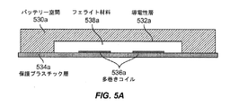
図5A、図5B、図5C、および図5Dは、本発明の例示的な実施形態による、バッテリーに対する誘導コイルおよびフェライト材料の配置に関する例示的な構成の図である。図5Aは、完全なフェライト埋込み型誘導コイル536aを示している。ワイヤレス電力誘導コイルは、フェライト材料538aおよびフェライト材料538aの辺りに巻かれたコイル536aを含むことができる。コイル536a自体は、標準的なリッツワイヤから作られ得る。導電シールド532aは、車両の同乗者を過剰なEMF送信から保護するために提供される。導電シールディングは、プラスチックまたは複合物から作られた車両では特に有益であり得る。
5A, 5B, 5C, and 5D are illustrations of exemplary configurations relating to placement of induction coils and ferrite material relative to a battery, according to an exemplary embodiment of the present invention. FIG. 5A shows a complete ferrite embedded
図5Bは、結合を高めるための、および導電シールド532bにおける渦電流(熱放散)を減らすための最適に寸法決定されたフェライトプレート(すなわち、フェライトバッキング)を示している。コイル536bは、非導電性の非磁性(たとえば、プラスチック)材料に完全に埋め込まれ得る。たとえば、図5A〜図5Dに示すように、コイル536bは、保護筐体534bに埋め込まれ得る。磁気結合とフェライトヒステリシス損との間のトレードオフの結果として、コイル536bとフェライト材料538bとの間に分離があり得る。
FIG. 5B shows an optimally sized ferrite plate (ie, ferrite backing) to increase coupling and reduce eddy currents (heat dissipation) in the
図5Cは、コイル536c(たとえば、銅リッツワイヤ多巻きコイル)が横(「X」)方向で移動可能であり得る別の実施形態を示している。図5Dは、誘導コイルモジュールが下方向に配置される別の実施形態を示している。いくつかの実施形態では、バッテリーユニットは、ワイヤレス電力インターフェースの一部として、配置可能な電気車両誘導コイルモジュール540dおよび配置不可能な電気車両誘導コイルモジュール540dのうちの1つを含む。磁場がバッテリー空間530dに、また車両の内部に浸透するのを防ぐために、バッテリー空間530dと車両との間に導電シールド532d(たとえば、銅板)があり得る。さらに、導電シールド532d、コイル536d、およびフェライト材料538dを環境の影響(たとえば、機械的損傷、酸化など)から保護するために、非導電(たとえば、プラスチック)保護層533dが使用され得る。さらに、コイル536dは、横X方向および/またはY方向に移動可能であり得る。図5Dは、電気車両誘導コイルモジュール540dがバッテリーユニット本体に対して下方Z方向に配置された一実施形態を示している。
FIG. 5C illustrates another embodiment where the coil 536c (eg, a copper litz wire multi-turn coil) may be movable in the lateral (“X”) direction. FIG. 5D shows another embodiment in which the induction coil module is arranged in the downward direction. In some embodiments, the battery unit includes one of a deployable electric vehicle
この配置可能な電気車両誘導コイルモジュール542bの設計は、電気車両誘導コイルモジュール542dに導電シールディングがないことを除いて、図5Bの設計と同様である。導電シールド532dは、バッテリーユニット本体に付帯している。電気車両誘導コイルモジュール542dが配置状態にないときに、保護層533d(たとえば、プラスチック層)は、導電シールド432dと電気車両誘導コイルモジュール542dとの間に提供される。電気車両誘導コイルモジュール542をバッテリーユニット本体から物理的に分離することは誘導コイルのパフォーマンスに好ましい影響を有し得る。
The design of this placeable electric vehicle induction coil module 542b is similar to the design of FIG. 5B, except that the electric vehicle
上で論じたように、配置された電気車両誘導コイルモジュール542dは、コイル536d(たとえば、リッツワイヤ)およびフェライト材料538dのみを含むことがある。フェライトバッキングは、結合を高めるために、および車体の底面または導電シールド532dにおける過剰な渦電流損から保護するために提供され得る。さらに、電気車両誘導コイルモジュール542dは、電力変換電子機器およびセンサ電子機器への柔軟なワイヤ接続を含み得る。このワイヤ束は、電気車両誘導コイルモジュール542dを配置するための機械ギアに組み込まれ得る。
As discussed above, the deployed electric vehicle
図1を参照すると、上述の充電システムは、電気車両112を充電するために、または電力網に戻すように電力を伝達するために、様々な場所で使用され得る。たとえば、電力の伝達は、駐車場環境で生じることがある。「駐車エリア」は、本明細書で「駐車スペース」と呼ばれることもあることに留意されたい。車両ワイヤレス電力伝達システム100の効率性を高めるために、電気車両112は、電気車両112内の電気車両誘導コイル116が関連駐車エリア内の基地ワイヤレス充電システム102aと適切に位置合わせできるようにX方向およびY方向に沿って位置合わせされ得る。
Referring to FIG. 1, the charging system described above can be used at various locations to charge the
さらに、開示する実施形態は、1つもしくは複数の駐車スペースまたは駐車エリアを有する駐車場に適用可能であり、駐車場内の少なくとも1つの駐車スペースは基地ワイヤレス充電システム102aを含むことができる。案内システム(図示せず)を使用して、電気車両112内の電気車両誘導コイル116が基地ワイヤレス充電システム102aと位置合わせされるように、車両オペレータが電気車両112を駐車エリアに位置付けるのを支援することができる。案内システムは、電気車両112内の電気車両誘導コイル116が充電基地(たとえば、基地ワイヤレス充電システム102a)内の充電誘導コイルと適切に位置合わせされ得るように、電気車両オペレータが電気車両112を位置付けるのを支援するための、電子基地の手法(たとえば、無線測位、方向発見原理、ならびに/または光学、準光学および/もしくは超音波感知方法)または機械基地の手法(たとえば、車輪ガイド、トラックまたはストップ)、あるいはそれらの任意の組合せを含むことができる。
Further, the disclosed embodiments are applicable to parking lots having one or more parking spaces or parking areas, where at least one parking space in the parking lot can include a base
上記で論じたように、電気車両充電システム114は、電力を送信し、かつ基地ワイヤレス充電システム102aから電力を受信するために、電気車両112の下面に配置され得る。たとえば、電気車両誘導コイル116は、好ましくは中心位置の近くで車体底面に組み込まれてよく、それにより、EM露出に関して最大の安全な距離がもたらされ、電気車両の前進駐車および後進駐車が可能になる。
As discussed above, the electric vehicle charging system 114 may be located on the underside of the
図6は、本発明の例示的な実施形態による、電気車両をワイヤレス充電するために使用され得る例示的な周波数を示す周波数スペクトルのチャートである。図6に示すように、電気車両へのワイヤレス高電力伝達のための潜在的周波数範囲は、3kHz〜30kHz帯域のVLF、いくつかの除外がある30kHz〜150kHz帯域の低LF(ISMなどの用途)、HFの6.78MHz(ITU−R ISM−帯域6.765〜6.795MHz)、HFの13.56MHz(ITU−R ISM−帯域13.553〜13.567)、およびHFの27.12MHz(ITU−R ISM−帯域26.957〜27.283)を含み得る。 FIG. 6 is a frequency spectrum chart illustrating exemplary frequencies that may be used to wirelessly charge an electric vehicle, according to an exemplary embodiment of the present invention. As shown in FIG. 6, the potential frequency range for wireless high power transfer to an electric vehicle is a VLF in the 3 kHz to 30 kHz band, a low LF in the 30 kHz to 150 kHz band with some exclusions (applications such as ISM) HF, 6.78 MHz (ITU-R ISM-band 6.765-6.795 MHz), HF 13.56 MHz (ITU-R ISM-band 13.553-13.567), and HF 27.12 MHz ( ITU-R ISM-band 26.957-27.283).
図7は、本発明の例示的な実施形態による、電気車両をワイヤレス充電するのに有用であり得る例示的な周波数および送信距離を示すチャートである。電気車両のワイヤレス充電に有用であり得るいくつかの例示的な送信距離は、約30mm、約75mm、および約150mmである。いくつかの例示的な周波数は、VLF帯域の約27kHzおよびLF帯域の約135kHzであり得る。 FIG. 7 is a chart illustrating exemplary frequencies and transmission distances that may be useful for wirelessly charging an electric vehicle according to an exemplary embodiment of the present invention. Some exemplary transmission distances that may be useful for wireless charging of electric vehicles are about 30 mm, about 75 mm, and about 150 mm. Some exemplary frequencies may be about 27 kHz for the VLF band and about 135 kHz for the LF band.
誘導電力伝達(IPT)システムは、エネルギーのワイヤレス伝達のための1つの方法を提供する。IPTシステムでは、1次(または「送信機」)電力デバイスが、2次(または「受信機」)電力受信機デバイスに電力を送信する。送信機電力デバイスおよび受信機電力デバイスの各々は誘導結合器、たとえば、電流搬送媒体のシングルコイル構成またはマルチコイル構成の巻線を含む。1次インダクタ内の交流電流は、交流磁場を生成する。2次インダクタが1次インダクタに近接して配置されたとき、交流磁場は2次インダクタ内に起電力(EMF)を誘起し(ファラデーの法則)、それによって2次電力受信機デバイスに電力を伝達する。 Inductive power transfer (IPT) systems provide one method for wireless transfer of energy. In an IPT system, a primary (or “transmitter”) power device transmits power to a secondary (or “receiver”) power receiver device. Each of the transmitter power device and the receiver power device includes an inductive coupler, eg, a single-coil or multi-coil winding of a current carrying medium. The alternating current in the primary inductor generates an alternating magnetic field. When the secondary inductor is placed in close proximity to the primary inductor, the alternating magnetic field induces an electromotive force (EMF) in the secondary inductor (Faraday's law), thereby transferring power to the secondary power receiver device. To do.
IPT磁束デバイスとも呼ばれる場合がある平面IPT結合器は、典型的には、磁束を生成または拾い上げるためのロープロファイル平面コイル構造と、フェライトバッキング構造またはコア構造と、磁束の成形および遮蔽のための導電性バックプレートとを備える。フェライト構造は、ギャップをほぼ伴わずに組み立てられた(たとえば、モノリシックブロックを構成する)フェライトタイルを備え得るか、または、フェライト構造は、磁束の主な方向がスラブの長辺に平行な状態で、スラブ間のギャップを伴うフェライトスラブを備え得る。導電性パックプレートは、地面と車体底面との間のスペース内の磁場のために所望される特定の境界条件を達成することを円滑にし得る。 Planar IPT couplers, which may also be referred to as IPT flux devices, typically have a low profile planar coil structure for generating or picking up magnetic flux, a ferrite backing structure or core structure, and a conductive for magnetic flux shaping and shielding. A back plate. The ferrite structure may comprise ferrite tiles assembled almost without gaps (eg, constituting a monolithic block), or the ferrite structure may have the main direction of magnetic flux parallel to the long side of the slab. A ferrite slab with a gap between the slabs may be provided. The conductive pack plate may facilitate achieving the specific boundary conditions desired for the magnetic field in the space between the ground and the bottom of the vehicle body.
地上基地充電ユニットから電気車両への誘導電力伝達(IPT)のために、様々な異なる平面コイル結合器トポロジーが提案されてきた。これらの結合器トポロジーは以下を含むが、これらに限定されない:すなわち、「円形」タイプ(たとえば、フェライトバッキングなど、フェライト構造の上部の上のシングルコイル、たとえば、米国特許出願第12/451,436号、「Multi−sourced electric vehicle pick−up」参照)、「ソレノイド」タイプ(たとえば、フェライトコアなど、フェライト構造周囲に巻かれたシングルコイル、たとえば、米国特許出願第13/138,299号、「Inductive power transfer apparatus」参照)、「二重コイル」タイプ(たとえば、フェライトバッキングなど、本質的に、フェライト構造の上部の上の2つのコイル、たとえば、米国特許出願第13/138,298号、「Inductive power transfer apparatus」参照)、およびそれらの変形態(たとえば、「双極」タイプ、たとえば、米国特許出願第13/389,090号、「Bi−polar pad development」参照)である。加えて、追加のコイルを備えたこれらのトポロジーの組合せであるIPTに関する他のコイル結合器トポロジーが提案されている(たとえば、「二重D」構造を「円形」構造と組み合わせる構成を開示する米国特許出願第13/791,538号、「Wireless power transfer system coil arrangements and method of operation」)。 A variety of different planar coil coupler topologies have been proposed for inductive power transfer (IPT) from ground-based charging units to electric vehicles. These coupler topologies include, but are not limited to: a “circular” type (eg, a single coil on top of a ferrite structure, such as a ferrite backing, eg, US patent application Ser. No. 12 / 451,436). No., “Multi-sourced electric pick-up”, “solenoid” type (for example, a single coil wound around a ferrite structure such as a ferrite core, eg, US patent application Ser. No. 13 / 138,299, “ “Inductive power transfer apparatus”), “double coil” type (eg, ferrite backing, essentially two coils on top of the ferrite structure, eg, US patent application Ser. No. 13/138 298 No., see "Inductive power transfer Apparatus"), and modified forms thereof (e.g., "bipolar" type, for example, U.S. Patent Application Serial No. 13 / 389,090, a "Bi-polar pad development" reference). In addition, other coil coupler topologies for IPT, which is a combination of these topologies with additional coils, have been proposed (e.g., US discloses a configuration combining a "double D" structure with a "circular" structure Patent application No. 13 / 791,538, “Wireless power transfer system coil arrangements and method of operation”).
同じサイズまたは体積の制約の下で最適化および比較される場合、これらの結合器トポロジーは、結合係数、水平変位ならびに垂直変位に対する許容(たとえば、オフセットおよびエアギャップ高さ)、固有品質値、ならびに車載の場合、車両の直近周囲のまたはその近傍の漏れ磁束密度(たとえば、放出)など、パフォーマンス特性の点で異なる。 When optimized and compared under the same size or volume constraints, these coupler topologies can be combined with coupling factors, horizontal and vertical displacement tolerances (eg, offset and air gap height), intrinsic quality values, and In the case of in-vehicle use, performance characteristics such as leakage magnetic flux density (for example, release) around or near the vehicle are different.
数々のコンピュータシミュレーション、ならびに、異なる結合器タイプのトポロジーおよび設計変形態の実際的な測定は、いくつかの実装形態では、「円形」タイプの結合器コイルは、概して、他のタイプの結合器に対して、一定の結合器トポロジーの結合は最も弱く、許容は最小であるが、放出は最低であり、Q値は最高であることを示すのに対して、「ソレノイド」タイプの結合器コイルは、他のタイプの結合器に対して、一定の結合器トポロジーの結合は最も強く、許容は最大であるが、放出レベルは最高であり、Q値は最低であることを示すという証拠を提供している。「二重コイル」タイプまたは「二重D」タイプの結合器コイルは、「円形」タイプの結合器コイルと「ソレノイド」タイプの結合器コイルとの間のやや中間であり、(たとえば、結合パフォーマンスと放出との間の)設計トレードオフを示すトポロジーとして、それらの結合器コイルを特に興味深いものにしている。 Numerous computer simulations and practical measurements of topological and design variations of different coupler types have shown that, in some implementations, “circular” type coupler coils are generally not compatible with other types of couplers. In contrast, the coupling of certain coupler topologies is the weakest and the tolerance is minimal, but the emission is the lowest, indicating the highest Q value, whereas the “solenoid” type coupler coil is For other types of couplers, it provides evidence that the coupling of a certain coupler topology is strongest and has the highest tolerance, but the highest emission level and the lowest Q value. ing. A “double coil” type or “double D” type coupler coil is somewhat intermediate between a “circular” type coupler coil and a “solenoid” type coupler coil (eg, coupling performance). These coupler coils are of particular interest as topologies showing the design trade-off (between and emission).
「二重コイル」タイプの結合器コイルのこの態様は、「円形」タイプのトポロジーと「ソレノイド」タイプのトポロジーとの間の変形の一段階として、「二重コイル」タイプの結合器トポロジーを考慮することによって説明され得る。「円形」タイプの結合器トポロジーおよび「ソレノイド」タイプの結合器トポロジーの変形としての「二重コイル」タイプの結合器トポロジーのこの説明は、様々な結合器トポロジーの特性を理解および説明する際に、またこれらの特性を系統的に選択(たとえば、制御)し、パフォーマンス特性間に(たとえば、結合係数と放出との間に)所望されるトレードオフを示す新しい結合器設計を生成するために有益であり得る。 This aspect of "double coil" type coupler coils considers "double coil" type coupler topologies as a step in the transformation between "circular" type topologies and "solenoid" type topologies. Can be explained. This description of the “double-coil” type coupler topology as a variation of the “circular” type coupler topology and the “solenoid” type coupler topology is in understanding and explaining the characteristics of the various coupler topologies. Also useful to systematically select (eg, control) these characteristics and generate a new coupler design that shows the desired trade-off between performance characteristics (eg, between coupling coefficient and emission) It can be.
図8Aは、その部材が「円形」タイプの結合器を「ソレノイド」タイプの結合器に変形させるプロセスの中間段階と見なされ得る、一群の「二重コイル」タイプの結合器設計を示す。具体的には、これらの結合器設計は、いわゆる「双極」結合器、および、特に興味深い、いわゆる「二重D」結合器の変形態である。 FIG. 8A shows a group of “double-coil” type coupler designs whose members can be considered intermediate stages of the process of transforming a “circular” type coupler into a “solenoid” type coupler. In particular, these coupler designs are variants of so-called “bipolar” couplers and, of particular interest, the so-called “double D” couplers.
2つの結合器トポロジーが特に興味深い:すなわち、「二重D、フルサイズフェライト」結合器トポロジーおよび「二重D、前面積層巻線」結合器トポロジーである。「二重D、フルサイズフェライト」結合器コイルは、放出に有利なトレードオフを表す、「二重D」タイプの結合器コイルの変形態と見なされ得る。「二重D、前面積層巻線」結合器コイルは、結合係数と変位に対する許容とに有利なトレードオフを表す、「二重D」タイプの結合器コイルの変形態と見なされ得る。基地パッド内に「二重D、フルサイズフェライト」結合器コイルを使用し、電気車両上に「二重D、前面積層巻線」結合器コイルを使用することは、両方の結合器コイルとパワーエレクトロニクス(たとえば、整流器)の両方と統合した小型車両パッケージに良好なソリューションを提供し得る。「二重D、前面積層巻線」結合器コイルの概念はまた、「二重D」タイプの結合器コイルと「四重極」タイプの結合器コイルの両方が最適スペース利用と良好なパフォーマンスとを備えた小型車両パッケージに統合されなければならない場合にも有用であり得る。 Two coupler topologies are of particular interest: a “double D, full size ferrite” coupler topology and a “double D, front laminated winding” coupler topology. A “double D, full size ferrite” coupler coil can be viewed as a variation of a “double D” type coupler coil that represents an advantageous trade-off for emissions. A “double D, front laminated winding” coupler coil can be viewed as a variation of a “double D” type coupler coil that represents an advantageous tradeoff between coupling coefficient and tolerance to displacement. Using a “Dual D, Full Size Ferrite” combiner coil in the base pad and using a “Dual D, Front Laminated Winding” combiner coil on an electric vehicle will result in both coupler coil and power It can provide a good solution for small vehicle packages integrated with both electronics (eg, rectifiers). The concept of “double D, front laminated winding” combiner coils also ensures that both “double D” type and “quadrupole” type combiner coils have optimal space utilization and good performance. It may also be useful if it has to be integrated into a small vehicle package with
「二重D、フルサイズフェライト」結合器(たとえば、図15A、図15B、および図25参照)は、磁束デバイス210の上方のスペースとの間で磁束を送信または受信するように構成された磁束デバイス210であり得る。本明細書で使用する「磁束デバイス」という用語は、基地パッド、車両パッド、または他のタイプの磁束パッドを含むが、これらに限定されない、その最も広い妥当な解釈を有し、任意の特定の形状、寸法、または構成要素の組合せに限定されない。本明細書で使用する「パッド」という用語は、ワイヤレス電気車両充電システムにおいて使用するように構成されたデバイス(たとえば、基地パッド、車両パッド)を含むが、これに限定されない、その最も広い妥当な解釈を有し、いかなる特定の形状、寸法、または構成要素の組合せにも限定されない。磁束デバイス210は、少なくとも第1の導電性コイル220と第2の導電性コイル230とを備える。第1のコイル220は、実質的に平面であり、第1のエリアの境界を画定する第1の外周を有する。第2のコイル230は、実質的に平面であり、第2のエリアの境界を画定する第2の外周を有する。第2のコイル230は、第1のコイル220と実質的に同一面上にある。磁束デバイス210は、実質的に平坦な面242を有し、第3のエリアの境界を画定する第3の外周を有する透磁性材料240をさらに備える。透磁性材料240は、本明細書で「コア」と呼ばれることがある。本明細書で使用する「コア」という用語は、具体的には、中央位置にあること、または他の構成要素によって包み込まれていることに限定されない、その最も広い妥当な解釈を有する。透磁性材料240は、少なくとも第1のコイル220および第2のコイル230に磁気的に関連付けられ得る。第1のコイル220および第2のコイル230は、実質的に平坦な面242に対して実質的に平行である。第3のエリアに対する第1のエリアおよび第2のエリアの総和比率は、0.9から1.1の範囲内である。
A “double D, full size ferrite” coupler (see, eg, FIGS. 15A, 15B, and 25) is configured to transmit or receive magnetic flux to and from the space above the
「二重D、前面積層巻線」結合器(たとえば、図17Aおよび図17B参照)は、磁束デバイス310の上方のスペースとの間で磁束を送信または受信するように構成された磁束デバイス310であり得る。本磁束デバイス310は、少なくとも第1の導電性コイル320と第2の導電性コイル330とを備える。第1のコイル320は、第1の層322と第2の層324とを有する。第2のコイル330は、第3の層332と第4の層334とを有する。第1の層322は、第3の層332と実質的に同一面上にある。磁束デバイス310は、実質的に平坦な第1の面342と、第1の縁部346において第1の面342に接触する第2の面344と、第2の縁部350において第1の面342に接触する第3の面348とを有する透磁性材料340をさらに備える。透磁性材料340は、少なくとも第1のコイル320および第2のコイル330に磁気的に関連付けられ得る。第1のコイル320は、第1の縁部346上に延び、第1の面342の平面に交差する。第2のコイル330は、第2の縁部350上に延び、第1の面342の平面に交差する。
A “double D, front layered winding” coupler (see, eg, FIGS. 17A and 17B) is a
図8Aは、平面「円形」トポロジーにおいて開始し、平面「ソレノイド」トポロジーにおいて終了する変形のプロセスを介して生成されていると見なされ得るIPTに関する「二重コイル」タイプの結合器トポロジーの選択を示す。この変形プロセスは、概して図8Bで概略的に表示される。初期ステップで、「円形」コイルは、第1のコイルと第2のコイルとに分割される。次いで、一方のコイルは左に動かされ、もう一方のコイルは右に動かされる。さらに、両方のコイルは、フェライト構造の幅に延ばされる。以下のステップで、内側区分(たとえば、隣接するコイル区分)の位置がフェライトの上部面上に固定された状態に留まり、外側区分(たとえば、反対側にあるコイル区分)がフェライト構造の下に動かされるように、コイルは、さらに延ばされ、フェライト構造上に引っ張られて、フェライト構造はコイルがコアの周囲に巻かれたコアになる。次のステップで、両方のコイルは、外側コイル区分が中央に向けて動かされ、2つに分離されているが、隣接するソレノイドコイルになるように収縮される。最終的に、2つのソレノイドコイルは単一のソレノイドにマージされる。パフォーマンスの比較可能性のために、変形によって生成されるすべての結合器は等しい形状因子を有すると仮定され得る。 FIG. 8A illustrates the selection of a “double-coil” type coupler topology for IPT that can be considered to have been generated through a process of deformation starting in a planar “circular” topology and ending in a planar “solenoid” topology. Show. This deformation process is generally represented schematically in FIG. 8B. In an initial step, the “circular” coil is divided into a first coil and a second coil. One coil is then moved to the left and the other coil is moved to the right. Furthermore, both coils are extended to the width of the ferrite structure. In the following steps, the position of the inner section (eg adjacent coil section) remains fixed on the top surface of the ferrite and the outer section (eg coil section on the opposite side) is moved under the ferrite structure. As such, the coil is further extended and pulled over the ferrite structure, which becomes the core with the coil wound around the core. In the next step, both coils are contracted so that the outer coil section is moved towards the center and separated into two but adjacent solenoid coils. Eventually, the two solenoid coils are merged into a single solenoid. For performance comparability, it can be assumed that all couplers produced by the deformation have equal form factors.
この変形プロセスはまた、図9A〜図9Bにおいて開始し、図23A〜図23Bにおいて終了する一連の概略図でも論証される。これらの概略図は、少なくとも結合器構造の断面図を示し、場合によっては、結合器の斜視(3D)図をさらに示す。断面図は、概して、一定の尺度で描かれておらず、定性的と見なされるべきである。 This deformation process is also demonstrated in a series of schematic diagrams starting in FIGS. 9A-9B and ending in FIGS. 23A-23B. These schematics show at least a cross-sectional view of the coupler structure and, in some cases, further show a perspective (3D) view of the coupler. Cross-sectional views are generally not drawn to scale and should be considered qualitative.
図9Aは、「円形」磁束デバイス(たとえば、図9Bの磁束デバイス)の断面を概略的に示す。図9Aはまた、磁束デバイスの中央の磁極エリア(N)と、磁束デバイスの周辺ゾーン内の対向極エリア(S)と、2本の特性磁力線とを示す。図8A〜図8Bの他のトポロジーと比較して、いくつかの構成では、すべてのトポロジーに関して同じサイズ(形状因子)と、同じ水平変位および垂直変位とを仮定して、「円形」磁束デバイスの対は、結合係数および許容は最低であるが、Q値は最高であり、放出レベル(たとえば、漏れ磁束)は最低であることを示し得る。低い放出レベルは、垂直磁場成分が導電性バックプレートによって効果的に消去され(たとえば、磁束整形効果)、IPT結合システムの機能スペースの外部により少ない漂遊磁束をもたらすということによって説明され得る。「円形」結合器は、したがって、図8A〜図8Bに示す一連のトポロジーにおける1つの極端な例と見なされ得る。 FIG. 9A schematically illustrates a cross-section of a “circular” flux device (eg, the flux device of FIG. 9B). FIG. 9A also shows the magnetic pole area (N) in the center of the magnetic flux device, the counter pole area (S) in the peripheral zone of the magnetic flux device, and two characteristic magnetic field lines. Compared to other topologies of FIGS. 8A-8B, in some configurations, assuming the same size (form factor) and the same horizontal and vertical displacement for all topologies, the “circular” flux device The pair may indicate that the coupling coefficient and tolerance are the lowest, but the Q value is the highest and the emission level (eg, leakage flux) is the lowest. The low emission level can be explained by the fact that the vertical field component is effectively erased by the conductive backplate (eg, flux shaping effect), resulting in less stray flux outside the functional space of the IPT coupling system. A “circular” coupler can therefore be considered as one extreme example in the series of topologies shown in FIGS. 8A-8B.
図10、図11、図12、および図13A〜図13Bは、「ソレノイド」への変形のステップ1、2、3、および4を概略的に示す:すなわち、「円形」コイルはコイルAとコイルBとに分割され(図10参照)、コイルAは左に動かされ(図11参照)、コイルBは右に動かされ(図12参照)、コイルBに重複しない、コイルAの部分はコイルBの平面まで下げられ(たとえば、調整され)(図13A〜図13B参照)、重複するコイルと、フェライト構造の外側寸法と実質的に等しい外側寸法とを備えた二重コイル構造をもたらす。ある程度の重複において、コイルAとコイルBとの間のほぼゼロ結合によって特徴付けられる、いわゆる「双極」磁束に遭遇する。ゼロ結合(たとえば、ゼロ相互インダクタンス)は、垂直モード、水平モード、またはそれらの混合モードの分極において「双極」結合器が動作できるように、コイルが異なる大きさおよび位相の電流とは無関係に駆動されることを可能にする。「双極」結合器のある例示的な実施形態のモデルを図13Bに示す。
10, 11, 12, and 13A-13B schematically illustrate
図13Aに示すように、コイルAとコイルBとが等しい電流レベルと電流方向で駆動される場合、「双極」結合器は、図13Aの極エリア(NおよびS)と磁力線とによって示す垂直磁気モーメントを生成する「円形」結合器のように機能する。「円形」結合器と同様に、これは、結合と変位許容とは比較的に弱いが、放出レベルが非常に低いことによって特徴付けられる。 As shown in FIG. 13A, when coil A and coil B are driven with equal current levels and directions, the “bipolar” coupler is the perpendicular magnetism indicated by the polar areas (N and S) and magnetic field lines of FIG. 13A. It functions like a “circular” coupler that generates moments. Similar to a “circular” coupler, this is characterized by a relatively low emission level, although coupling and displacement tolerance are relatively weak.
変形のステップ5で、図14に概略的に示すように、コイルBの電流方向は反転され、2つの極エリア(NおよびS)と磁力線とによって示されるように、水平分極モードで動作する「双極」結合器をもたらす。コイルのうちの1つの中の電流方向を変更することは、図8A〜図8Bに示した様々なトポロジーの最も著しい水平磁気モーメントを生成する「ソレノイド」タイプの結合器に一致し得るある種の挙動を引き起こし得る。したがって、「双極」結合器の特性は実質的に変化する。導電性バックプレートは水平磁界成分に関して何の漂遊磁場消去効果も有しないため、結合および許容は増大し、放出レベルも同様に増大する。対照的に、基地パッド内および車両パッド内の導電性バックプレートの使用、または、単に、車両底面および地面(たとえば、鉄筋コンクリート)内の金属構造の存在は、放出の点で、逆効果をまねく可能性がある。導電性バックプレートは、車両のスチール製の底面構造内および鉄筋コンクリート地面のスチール鉄筋構造内の過度の渦電流損失(たとえば、誘導加熱)を防ぐために使用され得る。他方で、導電性バックプレートの使用は、何らかの水平分極システム(たとえば、「ソレノイド」タイプ)の結合を実質的に改善することができ、金属構造が、概して、結合およびパフォーマンスに悪影響を与える「円形」タイプの磁束デバイスに対して、これらの結合器タイプの高い結合係数を部分的に説明し得る。
In
図15A〜図15Bは、非重複になり、両方のコイル220、230の外側水平寸法と透磁性材料240(たとえば、フェライト構造)とが実質的に互いに等しいことによって特徴付けられる「二重D、フルサイズフェライト」結合器と称するトポロジーをもたらす、2つのコイル220、230を修正する変形ステップ6の結果を概略的に示す。いくつかの事例では、「二重D」結合器のこの第1の変形態は「円形」タイプの結合器に「最も近接」しているため、この変形態は、図8A〜図8Bに示したシーケンスのすべての「二重D」変形態の中での最低放出レベルを示し得る。「二重D、フルサイズフェライト」トポロジーは、「ソレノイド」トポロジー、または「二重D」トポロジーの他の変形態と比べて、実質的により低い放出を生成するソリューションを提供する可能性を有するため、このトポロジーは、基地充電基地に有用であり得る。
FIGS. 15A-15B are non-overlapping and are characterized by the outer horizontal dimensions of both
図15A〜図15Bで示す例示的な構造では、第1のコイル220は、第1のエリアの境界を画定する(たとえば、D型の)第1の外周を有し、第2のコイル230は、第2のエリアの境界を画定する(たとえば、D型の)第2の外周を有し、透磁性材料240は、第3のエリアの境界を示す第3の外周を有し、第3のエリアに対する第1のエリアと第2のエリアの総和比率は0.9から1.1の範囲内である。たとえば、第1のエリアと第2のエリアの総和は、第3のエリアに実質的に等しい可能性がある。第1の外周の1つまたは複数の部分(たとえば、実質的に直線の部分)は、第3の外周の1つまたは複数の部分(たとえば、実質的に直線の部分)と実質的に整列し得、第2の外周の1つまたは複数の部分(たとえば、実質的に直線の部分)は第3の外周の1つまたは複数の部分(たとえば、実質的に直線の部分)に実質的に整列し得る。たとえば、第1のコイル220と第2のコイル230の総和の外側水平寸法(たとえば、第1の外周の実質的に直線の部分から、反対の、第2の外周の実質的に直線の部分までの二重Dコイルにわたる第1の長さ)は、透磁性材料240の外側水平寸法(たとえば、第1の長さに実質的に平行な第3の外周にわたる第2の長さ)に実質的に等しい可能性がある。第1の外周および第2の外周の他の部分(たとえば、D型の外周の角など、曲線部分)は、第1のエリアと第2のエリアの総和が第3のエリア未満になり得るように、第3の外周から外れてよい。
In the exemplary structure shown in FIGS. 15A-15B, the
図15A〜図15Bに示す例示的な構造では、透磁性材料240は、第3の外周と第3のエリアとを有するモノリシックフェライトプレートである。いくつかの他の構成では、透磁性材料240は、互いに機械的に結合されて、透磁性材料240を形成する複数の透磁性部分(たとえば、プレート、ロッド、ブロック、タイル)を備え得る。これらの複数の透磁性部分は、互いと少なくとも部分的に離間され得る。たとえば、透磁性材料240は、非透磁性材かつ非導電性の材料(たとえば、空気、プラスチック)を備える、少なくとも1つの領域を第3のエリア内に備え得る。少なくとも1つの領域は、互いに隣接する複数の領域、互いと別個である(たとえば、フェライト材料もしくは導電性材料によって分離された)複数の領域、またはそれら両方の複数の領域を備え得る。少なくとも1つの領域は、第3のエリアよりも20%少ない総和エリア(たとえば、少なくとも1つの領域のエリアの総和)を有し得る。
In the exemplary structure shown in FIGS. 15A-15B, the magnetically
図16A〜図16Bに概略的に示した変形ステップ7で、平面「二重D」巻線が基礎をなすフェライト構造にオーバーハングするように、フェライト構造の長さおよび幅はやや短縮される。このトポロジーは、「二重D、平面オーバーハンギング巻線」結合器と称され、「二重D」結合器の実施形態に対応する。このステップは、コイル巻線がフェライト上に引っ張られる、変形の以下の段階に関する予備手段と見なされ得る。フェライトのサイズを削減することは、所与のパッケージ形状因子制約の下でフェライトの前面において巻線用のスペースを提供する。興味深いことに、フェライトの修正は、結合と許容とを高めるが、(図13A〜図13Bに示したように)前述の「二重D」変形態に対して放出レベルも高める。
In the
「ソレノイド」タイプの結合器への途中のステップ8で、第1のコイルおよび第2のコイル320、330(たとえば、「二重Dコイル」の「Dコイル」)の外側区分が透磁性材料340(たとえば、フェライト構造)の前面上に引っ張られる。所与の磁束デバイス形状因子制約とコイル銅断面により、このステップは、多層(たとえば、積層)巻線構造に変形するように初期の「二重D」結合器の平面巻線構造を用いて実行され、その一例が図17A〜図17Bに概略的に示される、「二重D、前面積層巻線」トポロジーと称する、別の「二重D」変形態をもたらし得る。別の例示的な構造のより詳細な図が図26A〜図26Dに提供される。
In
この「二重D、前面積層巻線」結合器は、結合と許容の点で、「二重D、平面オーバーハンギング巻線」結合器よりも優れている可能性があるが、この結合器は「ソレノイド」タイプの結合器に「より近い」ことが見出されているため、より高い放出レベルを示す可能性がある。この変形ステップは、コイル開口を拡大し、コイル巻線(たとえば、第1のコイル320と第2のコイル330とを介して電流を搬送するコイル巻線のうちの少なくともいくつか)を透磁性材料340(たとえば、フェライト構造)の第1の面342を下回るほど下げ、磁極エリアを透磁性材料340の終端にシフトさせ、したがって、図17Aに示すように、より大きな磁束アーチをもたらす。巻線は導電性バックプレートにより近くなるため、この修正は渦電流損も増大させる場合がある。
This “double D, front layered winding” coupler may be superior to the “double D, planar overhanging winding” coupler in terms of coupling and tolerance, It has been found to be “closer” to “solenoid” type couplers, which may indicate higher discharge levels. This deformation step enlarges the coil opening and makes the coil winding (eg, at least some of the coil windings carrying current through the
車両パッケージに厳しい体積制約が存在する場合、この「二重D、前面積層巻線」トポロジーは、車両上での使用に特に適し、基地パッドよりもかなり小さい車両パッド形状因子にソリューションをもたらす。車両上に搭載された高結合タイプの「二重D」結合器(たとえば、その例を図17Aおよび図17Bに示す、「ソレノイド」または「二重D、前面積層巻線」磁束デバイス310)と組み合わされた、地面上の低放出タイプの「二重D」トポロジー(たとえば、その例を図15A、図15B、および図25に示す「二重D、フルサイズフェライト」磁束デバイス210)は、これらの状況の下で有用なソリューションを提供し得る。より大きな基地パッドは放出の主要源であり得、より小さい車両パッドは、主に結合および許容を受け持つことができる。したがって、基地側用に放出最適化されたトポロジーを使用し、車両側用に結合最適化されたトポロジーを使用する手法は、最適トレードオフとして有用であり得る。
This “dual D, front layered winding” topology is particularly suitable for use on vehicles and provides a solution for vehicle pad form factors that are significantly smaller than base pads when vehicle packages have severe volume constraints. A highly coupled “double D” coupler (eg, “solenoid” or “double D, front laminated winding”
図17A〜図17Bに示す例示的な構造では、第1のコイル320は、少なくとも1つのらせん巻線コイルを備え、第2のコイル330は、少なくとも1つのらせん巻線コイルを備える。たとえば、第1のコイル320は、複数の導電性巻線(たとえば、第1の層322および第2の層324)を備えることが可能であり、第2のコイル330は、複数の導電性巻線(たとえば、第3の層332および第4の層334)を備えることが可能である。いくつかの実施形態では、第のコイル320および第2のコイル330は、2つのコイルを形成するように巻かれた単一の導電性ワイヤによって形成される。第1のコイル320および第2のコイル330は両方とも、(たとえば、図17A〜図17Bに示すように、第1のコイルおよび第2のコイル320、330と透磁性材料340との間に介在材料を伴わずに、または介在材料を伴って)透磁性材料340に隣接し得る。第1のコイル320の第1の層322は、第1の面342の一方の半分の部分上に延びてよく、第2のコイル330の第3の層332は、第1の面342のもう一方の半分の部分上に延びてよい。第1のコイル320の第2の層324は、第1の面342の下に延び(たとえば、第1の面342の平面に交差し)、第2のコイル330の第4の層334は、第1の面342の下に延びる(たとえば、第1の面342の平面に交差する)。いくつかの実施形態では、第1のコイル320も第2のコイル330も、透磁性材料340を包囲しない(たとえば、第1の面342上から第1の面342の反対の透磁性材料340の底面の下に延びる)。図17A〜図17Bに示すように、第1のコイル320は、第1の面342上から第1の面342の下に延びてよく(たとえば、第1の面342の平面に交差してよく)、第1の縁部346において第1の面342に接触する第2の面344に隣接してよい(たとえば、第1の縁部346上に延びてよい)。加えて、第2のコイル330は、第1の面342上から第1の面342の下に延びてよく(たとえば、第1の面342の平面に交差してよく)、第2の縁部350において第1の面342に接触する第3の面348に隣接してよい(たとえば、第2の縁部350上に延びてよい)。いくつかの実施形態では、第1の縁部346は、図17A〜図17Bに概略的に示すように、第2の縁部350の反対であり得る。
In the exemplary structure shown in FIGS. 17A-17B, the
図17A〜図17Bに示す例示的な構造では、透磁性材料340は、モノリシックフェライトプレートである。いくつかの他の構成では、透磁性材料340は、互いに機械的に結合されて、透磁性材料340を形成する複数の透磁性部分(たとえば、プレート、ロッド、ブロック、タイル)を備え得る。これらの複数の透磁性部分は、互いと少なくとも部分的に離間され得る。たとえば、透磁性材料340は、非透磁性かつ非導電性の材料(たとえば、空気、プラスチック)を備える、少なくとも1つの領域を備え得る。少なくとも1つの領域は、互いに隣接する複数の領域、互いと別個である(たとえば、フェライト材料もしくは導電性材料によって分離された)複数の領域、またはそれら両方の複数の領域を備え得る。少なくとも1つの領域は、透磁性材料340の総エリアよりも20%少ない総和エリア(たとえば、少なくとも1つの領域のエリアの総和)を有し得る。
In the exemplary structure shown in FIGS. 17A-17B, the magnetically
いくつかの実施形態では、第1のコイル320の第1の層322は、第1の領域の境界を画定する第1の内周を有し、第2のコイル330の第3の層332は、第2の領域の境界を画定する第2の内周を有する。第1の領域の第1の中心点および第2の領域の第2の中心点は、それぞれ、透磁性材料340の中心点に対してよりも、第1の縁部346および第2の縁部350に対してより近い場合がある。いくつかの実施形態では、それぞれ、第1の層322および第3の層332内の第1のコイル320ならびに第2のコイル330の各々の少なくとも1つの巻きによって画定される第1の幾何平面は、実質的に平坦な第1の面342と平行である。
In some embodiments, the
図26A〜図26Cはそれぞれ、本明細書で説明するいくつかの実施形態による「二重D、前面積層巻線」結合器磁束デバイス310のモデルの透過トップダウン図、分解図、および斜視切断図を示す。第1のコイル320が第1の縁部346上に延び、第1の面342の平面に交差し、第2のコイル330が第2の縁部350上に延び、第1の面342の平面に交差するため、本明細書で説明するいくつかの実施形態は、「二重D、前面積層巻線」結合器磁束デバイス310を使用した小型車両パッケージ統合ソリューション内の電子機器に潜在的なスペースを提供する。そのような磁束デバイス310の一例の底面図は図26Dによって概略的に示されている。磁束デバイス310は、第1のコイル320と、第2のコイル330と、透磁性材料340とによって少なくとも部分的に境界が画定された1つまたは複数の領域360を備える。図26Dの1つまたは複数の領域360は、第1のコイル320および第2のコイル330の底面下の透磁性材料340の反対側に位置する。これらの領域は、電子部品(たとえば、磁束デバイス310の電力変換電子機器およびセンサ電子機器)を包含するように構成され得る。
26A-26C are each a transparent top-down, exploded, and perspective cut-away view of a model of a “double D, front laminated winding” coupler
ステップ9および10で「二重D」の変形を続けると、「二重D」巻線の外側区分をフェライトの前面上に完全に引っ張ることができ、フェライトを持ち上げて、フェライトの下に巻線用のスペースを作ることができる。コイルはフェライトコアの周囲に巻かれているため、図18に示す、結果として生じる新しいトポロジーは、「ソレノイド」タイプの結合器の変形態と見なされ得る。しかしながら、2つのコイルは非常に斜めであり、「二重ソレノイド、前面積層巻線」トポロジーと称する、前面積層巻線を依然として有する。磁束デバイスの全高(図18に示さず)が維持される場合、このステップはまた、コイルおよび/またはフェライト構造の厚みを減少させるステップを含み得る。加えて、外側巻線区分は、このとき、バックプレートに非常に近接する可能性があり、コイルのQ値に悪影響を有し得る。他方で、結合は実質的に増大され得、Q値の損失を部分的に補償し、依然として許容可能な効率性をもたらす。
Continuing the “double D” deformation in
以下のステップ(ステップ11、12、13、および14)で、フェライトの下のコイル区分が磁束デバイスの中央に向けて段階的に動かされるように、2つのソレノイドコイルは連続的に収縮され(たとえば、縮小され)、(フェライトの上の)中央区分を固定状態に維持する。この変形プロセスは、「二重ソレノイド」トポロジーのある変形態を形成することができ、最終的に「ソレノイド」トポロジーになる。ステップ10で、底部コイル区分は折り畳まれず(たとえば、単一平面内のすべての巻線)、図19A〜図19Dに概略的に示され、「二重ソレノイド、斜め巻線」と称する変形態をもたらす。ステップ11で、フェライトの長さはその「フルサイズ」に増大され、図20A〜図20Cに概略的に示すように、「二重ソレノイド、斜め巻線、フルサイズフェライト」と称するトポロジーをもたらす。このトポロジーは、「二重D、フルサイズフェライト結合器」(たとえば、図15A〜図15B、および図25参照)と類似と見なされ得る。ステップ12および13で、コイルはさらに収縮され、まず、「二重ソレノイド、わずかに斜め」結合器(たとえば、図20A〜図20C)をもたらし、次いで、「二重ソレノイド、コイル隣接」結合器をもたらす。最終的に、ステップ14で、2つのコイルはマージして、図8A〜図8Bに示す、最強の結合を提供するが、すべてのトポロジーの中で最高放出レベルも提供する単一の「ソレノイド」トポロジーになる。
In the following steps (
いくつかの実施形態では、(たとえば、その例が図17A〜図17Bおよび図26A〜図26Dによって概略的に示される)削減されたフェライト構造および積層巻線を備える「二重D前面積層巻線」構成のさらなる利点は、「DDQ」コイルが垂直磁束成分と水平磁束成分の両方を拾い上げることができるように、本明細書で「四重極」(Q)コイルと呼ばれる、「二重D」(DD)コイルと「円形」コイルの両方を統合する(「DDQ」コイル構成と呼ばれる)、いわゆる、交差分極結合器を設計する際に見出され得る。交差分極結合器は、x方向とy方向の両方に同時により多くの変位許容を提供する可能性を有する。この概念はまた基地(たとえば、一次)側に適用され得る。加えて、下でより十分に説明するように、交差分極結合器、すなわち、「DDQ」コイル構成は、(たとえば、最小エアスペースだけを開放状態に残すことによって)利用可能なスペースを最大可能範囲まで利用するために有用であり得る。 In some embodiments, a “double-D front laminated winding comprising a reduced ferrite structure and laminated winding (eg, examples are schematically illustrated by FIGS. 17A-17B and 26A-26D). A further advantage of the configuration is that a “double D”, referred to herein as a “quadrupole” (Q) coil, so that the “DDQ” coil can pick up both the vertical and horizontal flux components. It can be found in designing so-called cross-polarized couplers that integrate both (DD) coils and “circular” coils (referred to as “DDQ” coil configurations). Cross-polarized couplers have the potential to provide more displacement tolerance in both the x and y directions simultaneously. This concept can also be applied to the base (eg, primary) side. In addition, as described more fully below, a cross-polarized coupler, or “DDQ” coil configuration, maximizes the available space (eg, by leaving only the minimum air space open). Can be useful for up to.
図27A〜図27Cは、磁束デバイス410の上方のスペースとの間で電力をワイヤレスに受信または送信するための例示的な磁束デバイス410(たとえば、交差分極結合器、すなわち、「DDQ」コイル構成)を概略的に示す。磁束デバイス410は、磁場を介して電力をワイヤレスに受信または送信するように構成された第1の導電性構造420(たとえば、「DDコイル」)備える。第1の導電性構造420は、第1の下面を有する第1のコイル422(たとえば、第1のDコイル)と、第2の下面を有する第2のコイル424(たとえば、第2のDコイル)とを備える。第1のコイル420の第1の下面は、第2のコイル424の第2の下面と実質的に同一面上にある。第1の導電性構造420は、両方とも第1の下面および第2の下面と実質的に平行である、第1の長さ(L1)と第1の幅(W1)とを有し、第1の長さは第1の幅よりも大きい。磁束デバイス410は、磁場を介して電力をワイヤレスに受信または送信するように構成された第2の導電性構造440(たとえば、「Qコイル」)をさらに備える。第2の導電性構造440は、両方とも第1の下面および第2の下面と実質的に平行である、第2の長さ(L2)と第1の幅(W2)とを有し、第2の長さは第1の長さと実質的に平行であり、第2の幅よりも大きい。第1の導電性構造420の少なくとも第1の平面部分426は、第2の導電性構造430の第2の平面部分436と実質的に同一面上にある。
FIGS. 27A-27C illustrate an exemplary magnetic flux device 410 (eg, a cross-polarized coupler, or “DDQ” coil configuration) for wirelessly receiving or transmitting power to and from the space above the
いくつかの実施形態では、第1の導電性構造420は、第2の導電性構造440の実質的に平坦な面と平行であり、その面とは異なる層内にある第1の幾何平面を画定する、1つまたは複数の導電性巻線の第1の層を備え、第1の導電性構造420は、実質的に平坦な面によって画定された第3の幾何平面と少なくとも部分的に交差する(たとえば、それと同一面上にある)第2の幾何平面を画定する、1つまたは複数の導電性巻線の第2の層をさらに備える。第1の導電性構造420は、第1の領域の境界を画定する第1の内周を有し得、第2の導電性構造440は、第2の領域の境界を画定する第2の内周を有し得、第2の導電性構造440の1つまたは複数の導電性巻線は、第1の領域および第2の領域内に位置し、第1の層と実質的に同一面にあり、第2の層とは異なる層内に位置する。
In some embodiments, the first
いくつかの実施形態では、図27A〜図27Cに概略的に示すように、第1の導電性構造420(たとえば、第1のコイル422および第2のコイル424)ならびに第2の導電性構造440は、透磁性材料440の実質的に平坦な面442を実質的に完全に覆うように構成される。いくつかの実施形態では、図27A〜図27Cに概略的に示すように、第1の導電性構造420および第2の導電性構造430は互いの上に積層される。図27Cで理解できるように、第1の導電性構造420の第1の平面部分426は、第2の導電性構造430の第2の平面部分436を包含する少なくとも1つの領域の境界を少なくとも部分的に画定する。いくつかのそのような実施形態では、磁束デバイス410は、(たとえば、最小エアスペースだけを開放状態に残すことによって)利用可能なスペースを最大可能範囲まで利用することによって、最適スペース利用を有利に提供する。
In some embodiments, as schematically illustrated in FIGS. 27A-27C, a first conductive structure 420 (eg,
いくつかの実施形態では、図27Aに概略的に示すように、第1の長さは第2の長さよりも大きく、第1の幅は第2の幅に実質的に等しい。いくつかの実施形態では、第1のコイル422および第2のコイル424は、第1のエリアおよび第2のエリアをそれぞれ囲み、第2の導電性構造430は第3のエリアを囲む。第1の導電性構造420は、第1の導電性構造420の第1の長さに沿って延びる第1の幾何直線と各々が交差する、第1の縁部および第2の縁部を有し得る。いくつかの実施形態では、第1の幾何直線は第2の導電性構造430の第2の長さに沿って同様に延びるのに対して、いくつかの他の実施形態では、第1の幾何直線は、第2の導電性構造430の第2の長さに沿って延びる第2の幾何直線と実質的に平行である。いくつかの実施形態では、磁束デバイス410は、第1の導電性構造420と、第2の導電性構造430と、透磁性材料440とによって少なくとも部分的に境界が画定された、1つまたは複数の領域を備える。1つまたは複数の領域は、第1の導電性構造420および第2の導電性構造430の底面下の透磁性材料440の反対側に位置し得る。これらの領域は、電子部品(たとえば、磁束デバイス410の電力変換電子機器およびセンサ電子機器)を包含するように構成され得る。
In some embodiments, as schematically illustrated in FIG. 27A, the first length is greater than the second length, and the first width is substantially equal to the second width. In some embodiments, the
(たとえば、図27A〜図27Cに概略的に示す)「DDQ」コイル構成に対応するために、(たとえば、最小エアスペースだけを開放状態に維持することによって)利用可能なスペースを最大可能範囲まで利用することが有用であり得る。フェライトおよび銅(たとえば、リッツワイヤ)用に利用可能なスペースの最適利用は、(たとえば、車両パッケージに関する)厳しい形状因子制約に関して特に有用であり得る。したがって、フェライトの前面におけるスペースを積層巻線で充填することは、結合とスペース利用の両方の点で好ましい効果を備えた有用な手法であり得る。これは、図27Cの斜視切断図に示すように、「Q」コイルを「DD」コイルの開口内、およびフェライト構造の真上の同一面内に埋め込むための十分なスペースを提供することができる。この手法は、ロープロファイル磁束デバイスソリューションにとって有用であり得る。フェライトのサイズが削減されることにより、互いの上部にある「DD」コイル巻線および「Q」コイル巻線の側面区分に対応するために、磁束デバイスの各側上に何らかのスペースも存在し得る。フェライトの側面におけるスペースの最適利用は、図27Bで理解できるように、交互の積層コイル巻線により達成され得る。 To accommodate the “DDQ” coil configuration (e.g., schematically shown in FIGS. 27A-27C), make available space up to the maximum possible range (e.g., by keeping only the minimum air space open). It can be useful to utilize. Optimal utilization of available space for ferrite and copper (eg, litz wire) can be particularly useful with respect to severe form factor constraints (eg, for vehicle packages). Therefore, filling the space on the front surface of the ferrite with the laminated winding can be a useful technique with favorable effects in terms of both coupling and space utilization. This can provide sufficient space to embed the “Q” coil in the opening of the “DD” coil and in the same plane directly above the ferrite structure, as shown in the perspective cutaway view of FIG. 27C. . This approach may be useful for low profile flux device solutions. By reducing the size of the ferrite, there may also be some space on each side of the flux device to accommodate the side sections of the “DD” and “Q” coil windings on top of each other. . Optimal utilization of space on the sides of the ferrite can be achieved with alternating laminated coil windings, as can be seen in FIG. 27B.
上記の方法の様々な動作は、様々なハードウェアおよび/もしくはソフトウェアの構成要素、回路、ならびに/またはモジュールなどの、動作を実行することが可能な任意の適切な手段によって実行され得る。一般に、図に示す任意の動作は、それらの動作を実行することが可能な対応する機能手段によって実行され得る。たとえば、少なくとも1つの電流を流すための手段、または電流を導くための手段は、導電性コイルを備え得る。加えて、磁束を修正するための手段または磁束をチャンネリングするための手段は、透磁性材料を備え得る。加えて、電力をワイヤレスに送信または受信するための手段は、ワイヤレス電気送信機またはワイヤレス電気受信機を備え得る。 The various operations of the methods described above may be performed by any suitable means capable of performing operations, such as various hardware and / or software components, circuits, and / or modules. In general, any operations shown in the figures may be performed by corresponding functional means capable of performing those operations. For example, the means for passing at least one current or the means for directing current may comprise a conductive coil. In addition, the means for modifying the magnetic flux or the means for channeling the magnetic flux may comprise a magnetically permeable material. In addition, the means for transmitting or receiving power wirelessly may comprise a wireless electrical transmitter or a wireless electrical receiver.
様々な異なる技術および技法のうちのいずれかを使用して、情報および信号が表され得る。たとえば、上記の説明全体にわたって言及され得るデータ、命令、コマンド、情報、信号、ビット、シンボル、およびチップは、電圧、電流、電磁波、磁場もしくは磁性粒子、光学場もしくは光学粒子、またはそれらの任意の組合せによって表され得る。 Information and signals may be represented using any of a variety of different technologies and techniques. For example, data, instructions, commands, information, signals, bits, symbols, and chips that may be referred to throughout the above description are voltages, currents, electromagnetic waves, magnetic fields or magnetic particles, optical fields or optical particles, or any of them Can be represented by a combination.
本明細書で開示する実施形態に関して説明する様々な例示的論理ブロック、モジュール、回路、およびアルゴリズムステップは、電子ハードウェア、コンピュータソフトウェア、またはその両方の組合せとして実装され得る。ハードウェアおよびソフトウェアのこの互換性を明確に示すために、様々な例示的な構成要素、ブロック、モジュール、回路、およびステップについて、上記では概してそれらの機能性に関して説明した。そのような機能がハードウェアとして実装されるか、またはソフトウェアとして実装されるかは、具体的な適用例および全体的なシステムに課される設計の制約に依存する。説明した機能は特定の適用例ごとに様々な方法で実装され得るが、そのような実装の決定は、本発明の実施形態の範囲からの逸脱を生じるものと解釈されるべきではない。 Various exemplary logic blocks, modules, circuits, and algorithm steps described with respect to the embodiments disclosed herein may be implemented as electronic hardware, computer software, or a combination of both. To clearly illustrate this interchangeability of hardware and software, various illustrative components, blocks, modules, circuits, and steps have been described above generally in terms of their functionality. Whether such functionality is implemented as hardware or software depends upon the particular application and design constraints imposed on the overall system. Although the described functionality can be implemented in a variety of ways for a particular application, such implementation decisions should not be construed as causing a departure from the scope of the embodiments of the invention.
本明細書で開示する実施形態に関して説明する様々な例示的なブロック、モジュール、および回路は、汎用プロセッサ、デジタル信号プロセッサ(DSP)、特定用途向け集積回路(ASIC)、フィールドプログラマブルゲートアレイ(FPGA)もしくは他のプログラマブル論理デバイス、個別ゲートもしくはトランジスタ論理、個別ハードウェア構成要素、または、本明細書で説明した機能を実行するように設計されたそれらの任意の組合せで、実装あるいは実行され得る。汎用プロセッサはマイクロプロセッサとすることができるが、代替形態では、プロセッサは任意の従来のプロセッサ、コントローラ、マイクロコントローラ、または状態機械とすることができる。プロセッサは、また、たとえば、DSPとマイクロプロセッサの組合せ、複数のマイクロプロセッサの組合せ、1つもしくは複数のマイクロプロセッサのDSPコアと一緒の組合せ、またはそのような任意の他の構成など、コンピューティングデバイスの組合せとして実装されてもよい。 Various exemplary blocks, modules, and circuits described with respect to the embodiments disclosed herein include general purpose processors, digital signal processors (DSPs), application specific integrated circuits (ASICs), field programmable gate arrays (FPGAs). Alternatively, it may be implemented or implemented with other programmable logic devices, individual gate or transistor logic, individual hardware components, or any combination thereof designed to perform the functions described herein. A general purpose processor may be a microprocessor, but in the alternative, the processor may be any conventional processor, controller, microcontroller, or state machine. The processor may also be a computing device such as, for example, a combination of a DSP and a microprocessor, a combination of multiple microprocessors, a combination with a DSP core of one or more microprocessors, or any other configuration as such May be implemented as a combination.
本明細書で開示する実施形態に関して説明した方法またはアルゴリズムおよび機能のステップは、直接ハードウェアで具現化されても、プロセッサによって実行されるソフトウェアモジュールで具現化されても、またはその2つの組合せで具現化されてもよい。ソフトウェアで実装される場合、それらの機能は、1つもしくは複数の命令またはコードとして有形の非一時的コンピュータ可読媒体上に記憶されるか、または有形の非一時的コンピュータ可読媒体を介して送信される場合がある。ソフトウェアモジュールは、ランダムアクセスメモリ(RAM)、フラッシュメモリ、読取り専用メモリ(ROM)、電気的プログラマブルROM(EPROM)、電気的消去可能プログラマブルROM(EEPROM)、レジスタ、ハードディスク、リムーバブルディスク、CD ROM、または、当技術分野で既知である任意の、他の形態の記憶媒体中に存在し得る。記憶媒体は、プロセッサが記憶媒体から情報を読み取り、かつ記憶媒体に情報を書き込むことができるように、プロセッサに結合される。代替形態では、記憶媒体はプロセッサと一体にすることができる。本明細書で使用するディスク(disk)およびディスク(disc)は、コンパクトディスク(disc)(CD)、レーザディスク(disc)、光ディスク(disc)、デジタル多用途ディスク(disc)(DVD)、フロッピーディスク(disk)およびブルーレイディスク(disc)を含み、ディスク(disk)は、通常、データを磁気的に再生し、ディスク(disc)は、データをレーザで光学的に再生する。上述したものの組合せも、コンピュータ可読媒体の範囲の中に含められるべきである。プロセッサおよび記憶媒体はASIC内に存在し得る。そのASICはユーザ端末内に存在することができる。代替として、プロセッサおよび記憶媒体は、ユーザ端末内に個別構成要素として存在し得る。 The method or algorithm and functional steps described with respect to the embodiments disclosed herein may be implemented directly in hardware, software modules executed by a processor, or a combination of the two. It may be embodied. If implemented in software, the functions may be stored as one or more instructions or code on a tangible non-transitory computer readable medium or transmitted via a tangible non-transitory computer readable medium. There is a case. The software module can be random access memory (RAM), flash memory, read only memory (ROM), electrically programmable ROM (EPROM), electrically erasable programmable ROM (EEPROM), register, hard disk, removable disk, CD ROM, or It can be present in any other form of storage medium known in the art. A storage medium is coupled to the processor such that the processor can read information from, and write information to, the storage medium. In the alternative, the storage medium may be integral to the processor. As used herein, the disc and the disc are a compact disc (disc) (CD), a laser disc (disc), an optical disc (disc), a digital versatile disc (DVD), and a floppy disc. (Disk) and Blu-ray disc (disc), the disc (disk) normally reproduces data magnetically, and the disc (disc) optically reproduces data with a laser. Combinations of the above should also be included within the scope of computer-readable media. The processor and storage medium may reside in an ASIC. The ASIC can exist in the user terminal. In the alternative, the processor and the storage medium may reside as discrete components in a user terminal.
本開示の概要を示すために、本発明のいくつかの態様、利点、および新規の特徴が本明細書に記載されている。本発明の任意の特定の実施形態に従って、そのような利点の必ずしもすべてが実現されない場合があることを理解されたい。したがって、本発明は、本明細書に教示された1つの利点または利点のグループを、本明細書に教示または示唆され得る他の利点を必ずしも実現することなく、実現または最適化するように具現化または実行することができる。 In order to provide an overview of the disclosure, certain aspects, advantages, and novel features of the invention are described herein. It should be understood that not all such advantages may be realized in accordance with any particular embodiment of the present invention. Accordingly, the present invention may be implemented to realize or optimize one advantage or group of advantages taught herein without necessarily realizing the other advantages that may be taught or suggested herein. Or can be performed.
上述された実施形態の様々な修正が容易に明らかになり、本明細書に定義された一般原理は、本発明の趣旨または範囲を逸脱することなく、他の実施形態に適用することができる。したがって、本発明は、本明細書に示された実施形態に限定されるものではなく、本明細書に開示された原理および新規の特徴に一致する最大の範囲を与えられるものである。 Various modifications to the embodiments described above will be readily apparent and the general principles defined herein may be applied to other embodiments without departing from the spirit or scope of the invention. Accordingly, the present invention is not limited to the embodiments shown herein but is to be accorded the greatest scope consistent with the principles and novel features disclosed herein.
100 ワイヤレス電力伝達システム
102a、102b 基地ワイヤレス充電システム
104a 基地システム誘導コイル
110 電力リンク
112 電気車両
114 電気車両ワイヤレス充電システム
116 電気車両誘導コイル
118 バッテリーユニット
130 ローカル配電センター
132 電力バックボーン
200 ワイヤレス電力伝達システム
202 基地ワイヤレス電力充電システム
204 基地システム誘導コイル
206 基地システム送信回路
208 電源
210 磁束デバイス
214 電気車両充電システム
216 電気車両誘導コイル
218 電気車両バッテリーユニット、バッテリーユニット
220 第1の導電性コイル、第1のコイル
222 電気車両受信回路
230 第2の導電性コイル、第2のコイル
236 基地充電システム電力変換器、電力変換器
238 電気車両電力変換器
240 透磁性材料
242 実質的に平坦な面
300 ワイヤレス電力伝達システム
302 基地ワイヤレス充電システム
304 基地システム誘導コイル、基地誘導コイル
310 磁束デバイス
314 電気車両充電システム
316 電気車両誘導コイル
320 第1の導電性コイル、第1のコイル
322 第1の層
324 第2の層
330 第2の導電性コイル、第2のコイル
332 第3の層
334 第4の層
336 充電システム電力変換器、基地充電システム電力変換器
338 電気車両電力変換器
340 透磁性材料
342 基地充電システムコントローラ、第1の面
344 電気車両コントローラ、第2の面
346 第1の縁部
348 第3の面
350 第2の縁部
352 位置合わせシステム、基地充電位置合わせシステム
354 位置合わせシステム、電気車両位置合わせシステム、基地充電システム電力インターフェース
356 通信リンク
362 基地充電案内システム
364 電気車両案内システム
366 案内リンク
372 基地充電通信システム
374 電気車両通信システム
376 通信リンク
410 磁束デバイス
412 電気車両
420 第1の導電性構造
422 電気車両バッテリーユニット、第1のコイル
424 バッテリーコンパートメント、第2のコイル
426 充電器/バッテリーコードレスインターフェース、ワイヤレス電力インターフェース、第1の平面部分
428 バッテリー/EVコードレスインターフェース
430 第2の導電性構造
436 第2の平面部分
440 第1の導電性構造
530d バッテリー空間
532a 導電シールド
532b 導電シールド
532d 導電シールド
533d 非導電(たとえば、プラスチック)保護層
534b 保護筐体
536a フェライト埋込み型誘導コイル、コイル
536b コイル
536c コイル
536d コイル
538a フェライト材料
538b フェライト材料
538d フェライト材料
542d 電気車両誘導コイルモジュール
DESCRIPTION OF SYMBOLS 100 Wireless power transfer system 102a, 102b Base wireless charging system 104a Base system induction coil 110 Power link 112 Electric vehicle 114 Electric vehicle wireless charging system 116 Electric vehicle induction coil 118 Battery unit 130 Local power distribution center 132 Power backbone 200 Wireless power transmission system 202 Base wireless power charging system 204 Base system induction coil 206 Base system transmission circuit 208 Power supply 210 Magnetic flux device 214 Electric vehicle charging system 216 Electric vehicle induction coil 218 Electric vehicle battery unit, battery unit 220 First conductive coil, first coil 222 Electric vehicle receiving circuit 230 Second conductive coil, second coil 236 Base charging system Power converter, power converter 238 electric vehicle power converter 240 permeable material 242 substantially flat surface 300 wireless power transfer system 302 base wireless charging system 304 base system induction coil, base induction coil 310 magnetic flux device 314 electric vehicle Charging system 316 Electric vehicle induction coil 320 First conductive coil, first coil 322 First layer 324 Second layer 330 Second conductive coil, second coil 332 Third layer 334 Fourth Layer 336 Charging system power converter, base charging system power converter 338 Electric vehicle power converter 340 Magnetic permeable material 342 Base charging system controller, first side 344 Electric vehicle controller, second side 346 First edge 348 Third surface 350 Second edge 352 Alignment System, base charging alignment system 354 alignment system, electric vehicle alignment system, base charging system power interface 356 communication link 362 base charging guidance system 364 electric vehicle guidance system 366 guidance link 372 base charging communication system 374 electric vehicle communication system 376 Communication link 410 magnetic flux device 412 electric vehicle 420 first conductive structure 422 electric vehicle battery unit, first coil 424 battery compartment, second coil 426 charger / battery cordless interface, wireless power interface, first planar portion 428 Battery / EV cordless interface 430 Second conductive structure 436 Second planar portion 440 First conductive structure 530d Battery space 532a Conductive shield 532b Conductive shield 532d Conductive shield 533d Non-conductive (for example, plastic) protective layer 534b Protective housing 536a Ferrite embedded induction coil, coil 536b Coil 536c Coil 536d Coil 538a Ferrite material 538d Ferrite material 538d Ferrite material 538d Ferrite material 538d Vehicle induction coil module
Claims (19)
少なくとも第1の導電性コイルおよび第2の導電性コイルであって、前記第1のコイルが第1の層と第2の層とを有し、前記第2のコイルが第3の層と第4の層とを有し、前記第1の層が前記第3の層と実質的に同一面上にある、少なくとも第1の導電性コイルおよび第2の導電性コイルと、
実質的に平坦な第1の面と、第1の縁部において前記第1の面に接触する第2の面と、第2の縁部において前記第1の面に接触する第3の面とを有する透磁性材料であって、前記第1のコイルが、前記第1の縁部上に延び、前記第1の面の平面に交差し、前記第2のコイルが、前記第2の縁部上に延び、前記第1の面の平面に交差する、透磁性材料と
を備え、
前記第1の縁部において、前記第1の面に面した前記第1の層の面が前記第1の面の少なくとも一部を覆い、前記第2の面に面した前記第2の層の面が前記第2の面の少なくとも一部を覆い、
前記第2の縁部において、前記第1の面に面した前記第3の層の面が前記第1の面の少なくとも一部を覆い、前記第3の面に面した前記第4の層の面が前記第3の面の少なくとも一部を覆う、磁束デバイス。 A magnetic flux device configured to transmit or receive magnetic flux to and from a space above the magnetic flux device,
At least a first conductive coil and a second conductive coil, wherein the first coil has a first layer and a second layer, and the second coil has a third layer and a second layer. At least a first conductive coil and a second conductive coil, wherein the first layer is substantially coplanar with the third layer;
A first surface that is substantially flat; a second surface that contacts the first surface at a first edge; and a third surface that contacts the first surface at a second edge. The first coil extends over the first edge, intersects the plane of the first surface, and the second coil extends to the second edge. A magnetically permeable material extending upward and intersecting a plane of the first surface ;
In the first edge, the surface of the first layer facing the first surface covers at least part of the first surface, and the surface of the second layer facing the second surface A surface covers at least a portion of the second surface;
In the second edge, the surface of the third layer facing the first surface covers at least part of the first surface, and the surface of the fourth layer facing the third surface. A magnetic flux device , wherein a surface covers at least a portion of the third surface .
前記透磁性材料が、第3のエリアの境界を画定する第3の外周を有し、前記第1のコイルおよび前記第2のコイルが、前記実質的に平坦な面と実質的に平行であり、前記第3のエリアに対する前記第1のエリアおよび前記第2のエリアの総和比率が0.9から1.1の範囲である、請求項1に記載の磁束デバイス。 The first coil is substantially flat and has a first perimeter that defines a boundary of the first area; the second coil is substantially flat; A second perimeter defining a boundary, the second coil being substantially coplanar with the first coil;
The magnetically permeable material has a third outer periphery defining a boundary of a third area, and the first coil and the second coil are substantially parallel to the substantially flat surface. The magnetic flux device according to claim 1, wherein a sum ratio of the first area and the second area to the third area is in a range of 0.9 to 1.1.
第1の下面が、第2の下面と実質的に同一面上にある、前記第1の下面を有する第1のコイルと、前記第2の下面を有する第2のコイルとを備える、磁場を介して電力をワイヤレスに受信または送信するように構成された第1の導電性構造であって、両方とも前記第1の下面および前記第2の下面と実質的に平行な第1の長さと第1の幅とを有し、前記第1の長さが前記第1の幅よりも大きい、第1の導電性構造と、
両方とも前記第1の下面および前記第2の下面と実質的に平行な第2の長さと第2の幅とを有する、前記磁場を介して電力をワイヤレスに受信または送信するように構成された第2の導電性構造であって、前記第2の長さが、前記第1の長さと実質的に平行であり、前記第2の幅よりも大きく、前記第1の導電性構造の少なくとも第1の平面部分が前記第2の導電性構造の第2の平面部分と実質的に同一面上にある、第2の導電性構造と、
実質的に平坦な第1の面と、第1の縁部において前記第1の面に接触する第2の面と、第2の縁部において前記第1の面に接触する第3の面とを有する透磁性材料と、
を備え、
前記第1のコイルが第1の層と第2の層とを有し、前記第2のコイルが第3の層と第4の層とを有し、前記第1の層が前記第3の層と実質的に同一平面上にあり、
前記第1のコイルが、前記第1の縁部上に延び、前記第1の面の平面に交差し、前記第2のコイルが、前記第2の縁部上に延び、前記第1の面の平面に交差し、
前記第1の縁部において、前記第1の面に面した前記第1の層の面が前記第1の面の少なくとも一部を覆い、前記第2の面に面した前記第2の層の面が前記第2の面の少なくとも一部を覆い、
前記第2の縁部において、前記第1の面に面した前記第3の層の面が前記第1の面の少なくとも一部を覆い、前記第3の面に面した前記第4の層の面が前記第3の面の少なくとも一部を覆う、磁束デバイス。 A magnetic flux device for wirelessly transmitting or receiving power to or from a space above the magnetic flux device,
A magnetic field comprising a first coil having the first lower surface and a second coil having the second lower surface, the first lower surface being substantially coplanar with the second lower surface. A first conductive structure configured to wirelessly receive or transmit power via a first length and a first length substantially parallel to the first lower surface and the second lower surface; A first conductive structure having a width of 1 and wherein the first length is greater than the first width;
Both configured to receive or transmit power wirelessly via the magnetic field having a second length and a second width substantially parallel to the first lower surface and the second lower surface A second conductive structure, wherein the second length is substantially parallel to the first length, greater than the second width, and at least a first of the first conductive structure; A second conductive structure, wherein one planar portion is substantially coplanar with a second planar portion of the second conductive structure ;
A first surface that is substantially flat; a second surface that contacts the first surface at a first edge; and a third surface that contacts the first surface at a second edge. A magnetically permeable material having
Equipped with a,
The first coil has a first layer and a second layer, the second coil has a third layer and a fourth layer, and the first layer is the third layer. Is substantially coplanar with the layer,
The first coil extends on the first edge and intersects the plane of the first surface, and the second coil extends on the second edge and the first surface. Intersect the plane of
In the first edge, the surface of the first layer facing the first surface covers at least part of the first surface, and the surface of the second layer facing the second surface A surface covers at least a portion of the second surface;
In the second edge, the surface of the third layer facing the first surface covers at least part of the first surface, and the surface of the fourth layer facing the third surface. A magnetic flux device, wherein a surface covers at least a portion of the third surface.
Applications Claiming Priority (5)
| Application Number | Priority Date | Filing Date | Title |
|---|---|---|---|
| US201361917280P | 2013-12-17 | 2013-12-17 | |
| US61/917,280 | 2013-12-17 | ||
| US14/461,243 | 2014-08-15 | ||
| US14/461,243 US9837204B2 (en) | 2013-12-17 | 2014-08-15 | Coil topologies for inductive power transfer |
| PCT/US2014/070011 WO2015094964A1 (en) | 2013-12-17 | 2014-12-12 | Coil topologies for inductive power transfer |
Publications (3)
| Publication Number | Publication Date |
|---|---|
| JP2017511595A JP2017511595A (en) | 2017-04-20 |
| JP2017511595A5 JP2017511595A5 (en) | 2018-01-11 |
| JP6565082B2 true JP6565082B2 (en) | 2019-08-28 |
Family
ID=53369331
Family Applications (1)
| Application Number | Title | Priority Date | Filing Date |
|---|---|---|---|
| JP2016538002A Active JP6565082B2 (en) | 2013-12-17 | 2014-12-12 | Coil topology for inductive power transfer |
Country Status (6)
| Country | Link |
|---|---|
| US (2) | US9837204B2 (en) |
| EP (2) | EP3084914B1 (en) |
| JP (1) | JP6565082B2 (en) |
| KR (1) | KR102000432B1 (en) |
| CN (1) | CN105981254B (en) |
| WO (1) | WO2015094964A1 (en) |
Families Citing this family (57)
| Publication number | Priority date | Publication date | Assignee | Title |
|---|---|---|---|---|
| US11476566B2 (en) | 2009-03-09 | 2022-10-18 | Nucurrent, Inc. | Multi-layer-multi-turn structure for high efficiency wireless communication |
| EP2730005B1 (en) * | 2011-07-08 | 2021-05-05 | Auckland UniServices Limited | Interoperability of magnetic structures for inductive power transfer systems |
| CN104271384B (en) | 2012-05-09 | 2017-10-10 | 丰田自动车株式会社 | Vehicle |
| US9837204B2 (en) * | 2013-12-17 | 2017-12-05 | Qualcomm Incorporated | Coil topologies for inductive power transfer |
| KR101762778B1 (en) | 2014-03-04 | 2017-07-28 | 엘지이노텍 주식회사 | Wireless communication and charge substrate and wireless communication and charge device |
| JP6623522B2 (en) * | 2015-01-26 | 2019-12-25 | セイコーエプソン株式会社 | Robots, robot systems and servers |
| JP6060195B2 (en) * | 2015-03-06 | 2017-01-11 | 本田技研工業株式会社 | Vehicle parking control device |
| EP3118867A1 (en) * | 2015-07-17 | 2017-01-18 | ABB Technology AG | Inductive power transfer system |
| WO2017023180A1 (en) * | 2015-08-06 | 2017-02-09 | Auckland Uniservices Limited | Hybrid inductive power transfer system |
| TW201725828A (en) * | 2015-08-13 | 2017-07-16 | 維電股份有限公司 | Wireless power enabled enclosures for mobile devices |
| CN105050372B (en) * | 2015-09-09 | 2019-05-17 | 宁波微鹅电子科技有限公司 | A kind of electro-magnetic screen layer and the wireless electric energy transmission device with electro-magnetic screen layer |
| US10759281B2 (en) * | 2016-01-19 | 2020-09-01 | Ford Global Technologies, Llc | Controlling operation of electrified vehicle travelling on inductive roadway to influence electrical grid |
| US10530178B2 (en) * | 2016-03-10 | 2020-01-07 | Wireless Advanced Vehicle Electrification, Inc. | Bi-plane wireless power transmission pad |
| DE102016205352A1 (en) * | 2016-03-31 | 2017-10-05 | Bayerische Motoren Werke Aktiengesellschaft | Primary coil unit |
| JP6532086B2 (en) * | 2016-04-28 | 2019-06-19 | 昭和飛行機工業株式会社 | Externally shielded non-contact power supply |
| US10358045B2 (en) | 2016-05-11 | 2019-07-23 | Witricity Corporation | Methods and apparatus for wirelessly transferring power |
| US10688874B2 (en) * | 2016-06-14 | 2020-06-23 | Intel Corporation | Vehicular inductive power transfer systems and methods |
| US10404100B2 (en) | 2016-06-15 | 2019-09-03 | Witricity Corporation | Double-D based pad magnetics for reduced emissions in flush mounted and buried wireless power transfer applications |
| US10439449B2 (en) * | 2016-08-10 | 2019-10-08 | Microsoft Technology Licensing, Llc | Coupling device modules for inductive data transmission |
| DE102016215285A1 (en) * | 2016-08-16 | 2018-02-22 | Audi Ag | Energy storage device for a motor vehicle and motor vehicle |
| US10622142B2 (en) * | 2016-09-26 | 2020-04-14 | Utah State University | Concrete-embedded wireless power transfer coil |
| KR102401219B1 (en) * | 2016-10-17 | 2022-05-23 | 현대자동차주식회사 | Secondary pad for wireless power transfer system and manufactuing method thereof |
| DE102016223534A1 (en) | 2016-11-28 | 2018-05-30 | SUMIDA Components & Modules GmbH | Inductive component and Sekundärresonatoreinrichtung for mounting on an electric motor vehicle |
| US10984946B2 (en) * | 2016-12-20 | 2021-04-20 | Witricity Corporation | Reducing magnetic flux density proximate to a wireless charging pad |
| US20180233961A1 (en) * | 2017-02-14 | 2018-08-16 | Aiguo Hu | Inductive power transfer |
| JP6825501B2 (en) * | 2017-07-03 | 2021-02-03 | トヨタ自動車株式会社 | Power transmission device and power receiving device |
| EP3679639B1 (en) * | 2017-09-06 | 2023-11-01 | Wireless Advanced Vehicle Electrification, Inc. | Wireless power transfer pad with ferrite chimney |
| US10720277B2 (en) * | 2017-09-08 | 2020-07-21 | Witricity Corporation | Ferrite arrangement in a wireless power-transfer structure to mitigate dimensional tolerance effects on performance |
| US10850634B2 (en) * | 2017-10-20 | 2020-12-01 | Toyota Motor Engineering & Manufacturing North America, Inc. | Multi-turn configurable grid charging coil |
| US11431196B2 (en) | 2017-12-01 | 2022-08-30 | Auckland Uniservices Limited | Misalignment tolerant hybrid wireless power transfer system |
| CN107947396A (en) * | 2017-12-05 | 2018-04-20 | 宁波微鹅电子科技有限公司 | A kind of electromagnetic screen, wireless charging transmitting terminal, receiving terminal and system |
| CA3124345A1 (en) | 2017-12-22 | 2019-06-27 | Wireless Advanced Vehicle Electrification, Inc. | Wireless power transfer pad with multiple windings |
| US11462943B2 (en) | 2018-01-30 | 2022-10-04 | Wireless Advanced Vehicle Electrification, Llc | DC link charging of capacitor in a wireless power transfer pad |
| US10875417B2 (en) | 2018-02-06 | 2020-12-29 | Witricity Corporation | Thermal feedback for power transfer optimization |
| US11437854B2 (en) | 2018-02-12 | 2022-09-06 | Wireless Advanced Vehicle Electrification, Llc | Variable wireless power transfer system |
| WO2019182388A1 (en) * | 2018-03-22 | 2019-09-26 | 엘지전자 주식회사 | Wireless charging pad and wireless charging device |
| US11332025B2 (en) * | 2018-04-09 | 2022-05-17 | The Research Foundation For Suny | Multi-directional wireless charging of vehicles and robots |
| US11451089B2 (en) * | 2018-05-09 | 2022-09-20 | Oticon A/S | Charger antenna unit, charger device, and device to be charged |
| CN108879980B (en) * | 2018-07-04 | 2024-04-02 | 信维通信(江苏)有限公司 | Wireless charging module structure |
| EP3623205B1 (en) * | 2018-09-12 | 2022-01-19 | Ningbo Geely Automobile Research & Development Co. Ltd. | A device for a wireless power transfer system |
| WO2020065631A1 (en) * | 2018-09-28 | 2020-04-02 | Auckland Uniservices Limited | Wireless power transfer coupling structures with reduced leakage flux |
| US11214163B2 (en) * | 2018-12-04 | 2022-01-04 | Cisco Technology, Inc. | Coil association in multisite stationary wireless power transfer (WPT) and (quasi-)dynamic WPT deployments |
| KR102046843B1 (en) * | 2019-01-22 | 2019-11-21 | (주)그린파워 | A wireless power transmetting and receiving magnetic pad for an electric vehicle |
| EP3795408A1 (en) * | 2019-09-23 | 2021-03-24 | Ningbo Geely Automobile Research & Development Co. Ltd. | A device for a wireless power transfer system for charging a vehicle |
| DE102019127004A1 (en) | 2019-10-08 | 2021-04-08 | Tdk Electronics Ag | Coil arrangement with reduced losses and stabilized coupling factor and system for wireless energy transmission |
| DE102019127001A1 (en) * | 2019-10-08 | 2021-04-08 | Tdk Electronics Ag | Magnetic coil with reduced losses and system for wireless energy transfer |
| CN111082535B (en) * | 2019-12-12 | 2022-10-28 | 国家电网有限公司 | Method and system for determining structural parameters of double DD couplers of wireless charging system |
| DE102020201753A1 (en) | 2020-02-12 | 2021-08-12 | Würth Elektronik eiSos Gmbh & Co. KG | Coil module and method for producing a coil arrangement |
| JP7000483B2 (en) * | 2020-03-18 | 2022-01-19 | 本田技研工業株式会社 | Parking support system |
| DE102020206747A1 (en) | 2020-05-29 | 2021-12-02 | Würth Elektronik eiSos Gmbh & Co. KG | Coil arrangement for wireless electromagnetic energy transmission |
| CN111786467B (en) * | 2020-07-24 | 2022-04-01 | 重庆华创智能科技研究院有限公司 | Wireless power transmission mechanism and high-voltage power-taking wireless power transmission system |
| KR102312981B1 (en) * | 2020-10-22 | 2021-10-15 | 더가우스 주식회사 | Wireless power reception apparatus and a method of manufacturing the same |
| CN113285529B (en) * | 2020-12-23 | 2022-07-05 | 国网福建省电力有限公司电力科学研究院 | Cascade type multi-source multi-load power supply method based on wireless power transmission |
| WO2022169979A1 (en) * | 2021-02-04 | 2022-08-11 | Hevo, Inc. | Transmitter assembly and methods for making and using the same |
| EP4295466A1 (en) * | 2021-02-16 | 2023-12-27 | Wireless Advanced Vehicle Electrification, LLC | Biplane wireless power transfer pad |
| US20220294267A1 (en) * | 2021-02-16 | 2022-09-15 | Wireless Advanced Vehicle Electrification, Llc | Triangular arrangements for wireless power transfer pads |
| EP4342053A1 (en) * | 2021-05-19 | 2024-03-27 | Kamil PODHOLA | Wireless electromagnetic energy transfer system |
Family Cites Families (32)
| Publication number | Priority date | Publication date | Assignee | Title |
|---|---|---|---|---|
| US6150794A (en) * | 1996-05-27 | 2000-11-21 | Sanyo Electric Co., Ltd. | Charging system for motor-driven vehicle |
| AUPR520301A0 (en) * | 2001-05-23 | 2001-06-14 | Cochlear Limited | Transceiver coil for auditory prosthesis |
| GB2388715B (en) * | 2002-05-13 | 2005-08-03 | Splashpower Ltd | Improvements relating to the transfer of electromagnetic power |
| US7952322B2 (en) * | 2006-01-31 | 2011-05-31 | Mojo Mobility, Inc. | Inductive power source and charging system |
| DE102006048829B4 (en) * | 2006-10-11 | 2016-05-25 | Thyssenkrupp Transrapid Gmbh | Receiving unit with a receiver coil for non-contact transmission of electrical energy and method for their preparation |
| JP2008210861A (en) * | 2007-02-23 | 2008-09-11 | Yonezawa Densen Kk | Coil having magnetic shield sheet |
| US8749334B2 (en) | 2007-05-10 | 2014-06-10 | Auckland Uniservices Ltd. | Multi power sourced electric vehicle |
| JP4896820B2 (en) * | 2007-05-29 | 2012-03-14 | ソニー・エリクソン・モバイルコミュニケーションズ株式会社 | Coil module device |
| JP5118394B2 (en) | 2007-06-20 | 2013-01-16 | パナソニック株式会社 | Non-contact power transmission equipment |
| JP5390818B2 (en) * | 2008-09-19 | 2014-01-15 | 矢崎総業株式会社 | Communication coil structure of wireless power transmission device |
| JP6230776B2 (en) | 2009-02-05 | 2017-11-15 | オークランド ユニサービシズ リミテッドAuckland Uniservices Limited | Inductive power transmission device |
| US9283858B2 (en) | 2009-02-05 | 2016-03-15 | Auckland Uniservices Ltd | Inductive power transfer apparatus |
| CN102577011B (en) | 2009-08-07 | 2019-02-22 | 奥克兰联合服务有限公司 | Inductive power transfer device |
| WO2012018268A1 (en) | 2010-08-05 | 2012-02-09 | Auckland Uniservices Limited | Inductive power transfer apparatus |
| CN103748765B (en) | 2011-06-14 | 2016-11-09 | 松下电器产业株式会社 | Communicator |
| EP2730005B1 (en) * | 2011-07-08 | 2021-05-05 | Auckland UniServices Limited | Interoperability of magnetic structures for inductive power transfer systems |
| KR101213090B1 (en) | 2011-07-14 | 2012-12-18 | 유한회사 한림포스텍 | Core assembly for wireless power transmission apparatus and wireless power transmission apparatus having the same |
| CN111293788B (en) | 2011-09-07 | 2023-11-03 | 奥克兰联合服务有限公司 | Magnetic field shaping for inductive power transfer |
| CN105609959B (en) * | 2011-09-09 | 2018-07-17 | 株式会社村田制作所 | Antenna assembly |
| US20150295416A1 (en) | 2011-10-07 | 2015-10-15 | Powerbyproxi Limited | Transmitter for an inductive power transfer |
| JP5954698B2 (en) | 2011-10-17 | 2016-07-20 | パナソニックIpマネジメント株式会社 | Non-contact power feeder and primary coil block of non-contact power feeder |
| DE102011054541A1 (en) * | 2011-10-17 | 2013-04-18 | Conductix-Wampfler Gmbh | Device for inductive transmission of electrical energy |
| WO2013095428A1 (en) * | 2011-12-21 | 2013-06-27 | Intel Corporation | Interleaved coil and ferrite configuration to facilitate near field coupling |
| JP5957976B2 (en) | 2012-03-08 | 2016-07-27 | 日産自動車株式会社 | Contactless power supply |
| JP5896226B2 (en) | 2012-03-30 | 2016-03-30 | 株式会社デンソー | Contactless power supply |
| JP6056100B2 (en) * | 2012-04-24 | 2017-01-11 | 株式会社太陽光機 | Spiral coil |
| TW201346949A (en) | 2012-05-07 | 2013-11-16 | Delta Electronics Inc | Magnetic element having heat-dissipating bobbin base |
| WO2014011059A1 (en) | 2012-07-09 | 2014-01-16 | Auckland Uniservices Limited | Flux coupling device and magnetic structures therefor |
| JP6099352B2 (en) | 2012-10-17 | 2017-03-22 | デクセリアルズ株式会社 | Electronic device and coil module |
| JP5958266B2 (en) * | 2012-10-17 | 2016-07-27 | 株式会社ダイフク | Non-contact power supply pad and non-contact charging system for forklift using the non-contact power supply pad |
| JP5958423B2 (en) * | 2013-06-10 | 2016-08-02 | 株式会社ダイフク | Non-contact power supply pad manufacturing method, non-contact power supply pad manufactured by the manufacturing method, and forklift non-contact charging system using the non-contact power supply pad |
| US9837204B2 (en) * | 2013-12-17 | 2017-12-05 | Qualcomm Incorporated | Coil topologies for inductive power transfer |
-
2014
- 2014-08-15 US US14/461,243 patent/US9837204B2/en active Active
- 2014-12-12 JP JP2016538002A patent/JP6565082B2/en active Active
- 2014-12-12 KR KR1020167019083A patent/KR102000432B1/en active IP Right Grant
- 2014-12-12 EP EP14821999.1A patent/EP3084914B1/en active Active
- 2014-12-12 WO PCT/US2014/070011 patent/WO2015094964A1/en active Application Filing
- 2014-12-12 EP EP18180725.6A patent/EP3402030A1/en active Pending
- 2014-12-12 CN CN201480066887.2A patent/CN105981254B/en active Active
-
2017
- 2017-11-03 US US15/803,648 patent/US10340078B2/en active Active
Also Published As
| Publication number | Publication date |
|---|---|
| US20150170833A1 (en) | 2015-06-18 |
| CN105981254A (en) | 2016-09-28 |
| CN105981254B (en) | 2019-04-23 |
| US20180137972A1 (en) | 2018-05-17 |
| WO2015094964A1 (en) | 2015-06-25 |
| EP3084914A1 (en) | 2016-10-26 |
| KR102000432B1 (en) | 2019-07-16 |
| US10340078B2 (en) | 2019-07-02 |
| US9837204B2 (en) | 2017-12-05 |
| EP3402030A1 (en) | 2018-11-14 |
| KR20160099663A (en) | 2016-08-22 |
| JP2017511595A (en) | 2017-04-20 |
| EP3084914B1 (en) | 2018-07-04 |
Similar Documents
| Publication | Publication Date | Title |
|---|---|---|
| JP6565082B2 (en) | Coil topology for inductive power transfer | |
| US10003217B2 (en) | System and method for reducing emissions for polarized coil systems for wireless inductive power transfer | |
| EP2992537B1 (en) | Vehicle charging pad having reduced thickness | |
| US9972434B2 (en) | Magnetically permeable structures | |
| US9376026B2 (en) | System and method for inductance compensation in wireless power transfer | |
| JP6420320B2 (en) | Systems, methods and apparatus for electric vehicle wired and wireless charging | |
| CA2920780C (en) | Systems and methods for bi-state impedance conversion in wireless power transfer | |
| JP2017517866A5 (en) | ||
| WO2014070443A2 (en) | Coil arrangements in wireless power transfer systems for low electromagnetic emissions | |
| US9742200B2 (en) | System and method to avoid magnetic power loss while providing alternating current through a ferromagnetic material |
Legal Events
| Date | Code | Title | Description |
|---|---|---|---|
| A521 | Request for written amendment filed |
Free format text: JAPANESE INTERMEDIATE CODE: A523 Effective date: 20171127 |
|
| A621 | Written request for application examination |
Free format text: JAPANESE INTERMEDIATE CODE: A621 Effective date: 20171127 |
|
| A977 | Report on retrieval |
Free format text: JAPANESE INTERMEDIATE CODE: A971007 Effective date: 20181122 |
|
| A131 | Notification of reasons for refusal |
Free format text: JAPANESE INTERMEDIATE CODE: A131 Effective date: 20181203 |
|
| A521 | Request for written amendment filed |
Free format text: JAPANESE INTERMEDIATE CODE: A523 Effective date: 20190301 |
|
| TRDD | Decision of grant or rejection written | ||
| A01 | Written decision to grant a patent or to grant a registration (utility model) |
Free format text: JAPANESE INTERMEDIATE CODE: A01 Effective date: 20190610 |
|
| A711 | Notification of change in applicant |
Free format text: JAPANESE INTERMEDIATE CODE: A711 Effective date: 20190710 |
|
| A61 | First payment of annual fees (during grant procedure) |
Free format text: JAPANESE INTERMEDIATE CODE: A61 Effective date: 20190710 |
|
| A521 | Request for written amendment filed |
Free format text: JAPANESE INTERMEDIATE CODE: A523 Effective date: 20190726 |
|
| R150 | Certificate of patent or registration of utility model |
Ref document number: 6565082 Country of ref document: JP Free format text: JAPANESE INTERMEDIATE CODE: R150 |
|
| R250 | Receipt of annual fees |
Free format text: JAPANESE INTERMEDIATE CODE: R250 |
|
| R250 | Receipt of annual fees |
Free format text: JAPANESE INTERMEDIATE CODE: R250 |