JP6564591B2 - Appearance inspection apparatus, appearance inspection method, and substrate unit - Google Patents
Appearance inspection apparatus, appearance inspection method, and substrate unit Download PDFInfo
- Publication number
- JP6564591B2 JP6564591B2 JP2015057017A JP2015057017A JP6564591B2 JP 6564591 B2 JP6564591 B2 JP 6564591B2 JP 2015057017 A JP2015057017 A JP 2015057017A JP 2015057017 A JP2015057017 A JP 2015057017A JP 6564591 B2 JP6564591 B2 JP 6564591B2
- Authority
- JP
- Japan
- Prior art keywords
- image
- visible light
- inspection
- inspection object
- imaging
- Prior art date
- Legal status (The legal status is an assumption and is not a legal conclusion. Google has not performed a legal analysis and makes no representation as to the accuracy of the status listed.)
- Expired - Fee Related
Links
- 238000007689 inspection Methods 0.000 title claims description 123
- 239000000758 substrate Substances 0.000 title description 62
- 238000000034 method Methods 0.000 title description 18
- 238000003384 imaging method Methods 0.000 claims description 72
- 238000005286 illumination Methods 0.000 claims description 56
- 230000003287 optical effect Effects 0.000 claims description 21
- 230000031700 light absorption Effects 0.000 description 20
- 238000010586 diagram Methods 0.000 description 16
- 238000012790 confirmation Methods 0.000 description 9
- 239000000126 substance Substances 0.000 description 8
- 230000005284 excitation Effects 0.000 description 7
- 238000004519 manufacturing process Methods 0.000 description 7
- 239000000463 material Substances 0.000 description 6
- 238000011179 visual inspection Methods 0.000 description 6
- 230000001678 irradiating effect Effects 0.000 description 4
- 238000007789 sealing Methods 0.000 description 4
- 238000001514 detection method Methods 0.000 description 3
- 239000011347 resin Substances 0.000 description 3
- 229920005989 resin Polymers 0.000 description 3
- 230000005540 biological transmission Effects 0.000 description 2
- 239000003153 chemical reaction reagent Substances 0.000 description 2
- 239000002184 metal Substances 0.000 description 2
- 238000001579 optical reflectometry Methods 0.000 description 2
- 238000012545 processing Methods 0.000 description 2
- 239000011248 coating agent Substances 0.000 description 1
- 238000000576 coating method Methods 0.000 description 1
- 239000003086 colorant Substances 0.000 description 1
- 238000012937 correction Methods 0.000 description 1
- 238000013500 data storage Methods 0.000 description 1
- 230000002950 deficient Effects 0.000 description 1
- 230000001419 dependent effect Effects 0.000 description 1
- 238000000684 flow cytometry Methods 0.000 description 1
- 239000007850 fluorescent dye Substances 0.000 description 1
- 238000012986 modification Methods 0.000 description 1
- 230000004048 modification Effects 0.000 description 1
- 238000000465 moulding Methods 0.000 description 1
- 239000003973 paint Substances 0.000 description 1
- 229910000679 solder Inorganic materials 0.000 description 1
- 238000012360 testing method Methods 0.000 description 1
Images


Landscapes
- Pinball Game Machines (AREA)
- Investigating Materials By The Use Of Optical Means Adapted For Particular Applications (AREA)
Description
本発明は、透明な容器とその内部に収納された部品からなる透明容器ユニットの外観を検査する技術に関し、特に、遊技機用基板の検査に好適な検査技術に関する。 The present invention relates to a technique for inspecting the appearance of a transparent container unit including a transparent container and components housed therein, and more particularly to an inspection technique suitable for inspecting a gaming machine substrate.
遊技機用基板は、基板に実装された電子部品の改ざん等を防止するために、及び、基板の交換を容易とする為に、基板ケースによって覆われている。以下に、基板ケースとそれに収納された基板の組立体を基板ユニットと称することとする。遊技機と基板との電気的な接合は基板ユニットのコネクタ部のみであり、基板ケースを破壊しないとROM等の電子部品への接触は出来ない。基板ケースは透明な樹脂又はプラスチックスにより形成され、基板に実装されたROM等の電子部品の視認が可能である。 The gaming machine substrate is covered with a substrate case to prevent tampering of electronic components mounted on the substrate and to facilitate replacement of the substrate. Hereinafter, the assembly of the substrate case and the substrate accommodated therein is referred to as a substrate unit. The electrical connection between the gaming machine and the board is only the connector part of the board unit, and the electronic parts such as ROM cannot be contacted unless the board case is destroyed. The substrate case is formed of a transparent resin or plastic, and an electronic component such as a ROM mounted on the substrate can be visually confirmed.
基板ケースは蓋部と底部からなり、両者は端部にて、カシメ又はクリップにより、機械的に接合されている。基板ケースの蓋部と底部の接合部に、封止紙が貼り付けられ、基板ケースが開けられたか否かを確認できる。基板は、基板ケースの底部にネジによって固定されている。 The substrate case is composed of a lid portion and a bottom portion, and both are mechanically joined at the end portion by caulking or a clip. It is possible to confirm whether or not the sealing paper has been attached to the joint between the lid and bottom of the substrate case and the substrate case has been opened. The substrate is fixed to the bottom of the substrate case with screws.
特許文献1(特開2003-230730号公報)には、封止の状態を確認することについて、封止証明の紙のほか、カシメの状態を確認することが記載されている。特許文献2(特開2003-346212号公報)には、有価証券上の紫外光もしくは赤外線にて励起するテープの検出について記載がされている。特許文献3〜5(特開平5-334330、特開2000-122419、特開2000-137821)には、登録された印影と押印された印影とのマッチングによる照合に関する技術が記載されている。 Patent Document 1 (Japanese Patent Laid-Open No. 2003-230730) describes confirming the state of caulking in addition to the paper of the seal certification for confirming the state of sealing. Patent Document 2 (Japanese Patent Laid-Open No. 2003-346212) describes detection of a tape excited by ultraviolet light or infrared light on a securities. Patent Documents 3 to 5 (Japanese Patent Laid-Open Nos. 5-334330, 2000-122419, and 2000-137821) describe a technique related to matching by matching a registered imprint and a stamped imprint.
遊技機用基板の製造ラインでは、基板ユニットの検査が行われる。検査項目は次のとおりである。
(イ)基板ケースの透明な蓋部に形成された刻印文字の有無の確認
(ロ)基板ケースの蓋部に貼付された基板の電気的、動作的な説明を記載したシールの有無と記載内容の確認
(ハ)基板ケースの透明な蓋部に貼付された識別情報を記載したシールの有無の確認と記載内容の確認
(ニ)基板ケースの透明な蓋部と底部を機械的に接合するカシメやクリップの有無の確認
(ホ)基板ケースの透明な蓋部に貼付された白地上の検印等の印影の有無の確認
In the production line for gaming machine boards, the board unit is inspected. The inspection items are as follows.
(A) Confirmation of the presence or absence of engraved characters formed on the transparent lid of the substrate case (b) Presence or absence of the seal describing the electrical and operational description of the substrate affixed to the lid of the substrate case (C) Confirmation of the presence or absence of a seal with identification information affixed to the transparent lid of the substrate case and confirmation of the description (d) Caulking to mechanically join the transparent lid and bottom of the substrate case (E) Confirmation of the presence or absence of imprints on white ground, etc. affixed to the transparent lid of the board case
本願の発明者は、先ず、(イ)基板ケースの透明な蓋部に形成された刻印文字の有無の確認を正確に行うという課題について考察した。刻印文字は、透視可能な透明樹脂で製作された基板ケースにレーザで刻印され、または基板ケース形成時に成型により形成される。刻印文字を撮像するとき、基板ケース上の刻印文字の像と基板の像が重なった画像が得られる。基板ケースの刻印文字とそれ以外の部分の撮像画像上のコントラストが小さいため、透視された基板の画像の映り込みの影響により、刻印文字を正確に認識することが困難である。この問題を解決する手段の記載は上記先行技術資料からは見つけられない。 The inventor of the present application first considered (a) the problem of accurately confirming the presence or absence of stamped characters formed on the transparent lid of the substrate case. The engraved characters are engraved with a laser on a substrate case made of a transparent resin that can be seen through, or formed by molding when the substrate case is formed. When the stamped character is imaged, an image in which the image of the stamped character on the substrate case and the image of the substrate overlap is obtained. Since the contrast on the picked-up image of the printed character of the board case and the other part is small, it is difficult to accurately recognize the printed letter due to the influence of the reflected image of the board. A description of means for solving this problem cannot be found from the above prior art documents.
次に、(ロ)(ハ)シールの有無の確認と(ニ)基板ケースのカシメ又はクリップの有無の確認を正確に行うという課題について考察した。特許文献1(特開2003-230730)には、撮像画像によりカシメの状態を確認すること記載されている。しかしながら、基板ケースの撮像画像ではコントラストが小さく、カシメ又はクリップの有無を精度良く検出できない。シールについても同様である。特許文献2(特開2003-346212)には、有価証券上の紫外光もしくは赤外線にて励起するテープの検出についての記載がされている。しかしながら、紫外光及び赤外線の画像処理システムに一般的に使用される各波長用のLED光源からは微量な可視領域の光が出射される。その可視光線が励起させ撮像しようとする対象以外の部分を照らすため、その部分の撮像画像が励起画像に写り込み、励起画像と重なり画像ノイズとなり認識精度を悪化させる問題がある。また、基板ケースの検査の場合、基板上の金属部品やリフロー済み半田などの高反射率の部分があるため、紫外光を反射し撮像画像に写り込み、励起画像と重なり画像ノイズとなり認識精度を悪化させる問題がある。 Next, (b) (c) the problem of accurately confirming whether or not there was a seal and (d) whether or not the board case was caulked or clipped was considered. Patent Document 1 (Japanese Patent Laid-Open No. 2003-230730) describes that a caulking state is confirmed from a captured image. However, in the captured image of the substrate case, the contrast is small and the presence or absence of caulking or clipping cannot be detected with high accuracy. The same applies to the seal. Patent Document 2 (Japanese Patent Laid-Open No. 2003-346212) describes detection of a tape that is excited by ultraviolet light or infrared light on a securities. However, a small amount of light in the visible region is emitted from the LED light source for each wavelength that is generally used in ultraviolet and infrared image processing systems. Since the visible light is excited to illuminate a portion other than the object to be imaged, the captured image of that portion is reflected in the excitation image, and overlaps with the excitation image, resulting in image noise, which deteriorates recognition accuracy. In the case of inspecting the substrate case, there are high-reflectance parts such as metal parts on the substrate and reflowed solder, so the ultraviolet light is reflected and reflected in the captured image, overlapping with the excitation image and resulting in image noise. There are problems that make it worse.
本願の発明者は、更に、(ホ)透明な基板ケースの上の検印等の印影の有無の確認を正確に行う課題について検討した。特許文献3〜5(特開平5-334330、特開2000-122419、特開2000-137821)には、マッチングによる印影の照合についての技術の記載がある。しかしながら、実施年月日が押印される検印の有無の確認の場合、検査実施日ごとに変更される実施年月日の部分がマッチング処理でマッチング率に影響しないようにするには、想定される実施年月日の印影をすべて登録し、登録した印影の数だけマッチング処理をし、最もマッチング率の良い印影で照合することとなり、膨大なデータの保持と膨大な検査時間を必要とする。また、実施年月日部分をマッチング対象外としてマッチング処理を実施する場合は、回転補正や位置検出の処理に時間がかかってしまい、検査時間がその分多く掛かってしまう問題がある。 The inventor of the present application further studied (e) a problem of accurately confirming the presence or absence of imprints such as a seal on a transparent substrate case. Patent Documents 3 to 5 (Japanese Patent Laid-Open Nos. 5-334330, 2000-122419, and 2000-137821) describe a technique for checking an imprint by matching. However, in the case of confirmation of the presence or absence of a seal where the implementation date is stamped, it is assumed that the portion of the implementation date changed for each inspection implementation date will not affect the matching rate in the matching process All the imprints of the implementation date are registered, matching processing is performed for the number of registered imprints, and collation is performed with the imprint with the best matching rate, and enormous data storage and enormous inspection time are required. Further, when the matching process is performed with the implementation date portion excluded from the matching target, there is a problem that the rotation correction and the position detection process take time, and the inspection time is increased accordingly.
検査の漏れ又は検査ミスが一件でも発覚した場合には、該当する基板ユニットを使用するシリーズの遊技機が設置された全国の店舗にて遊技機全台の確認・修復作業を要求される。そのため、莫大な損害を発生する。従来、製造ラインにおける基板ユニットの検査は、人の目視に依存していた。そこで、人の目視に頼らない正確な検査技術の必要性が高まっている。 If any inspection omission or inspection error is detected, all the gaming machines are required to be confirmed and repaired at stores nationwide where a series of gaming machines using the corresponding board unit is installed. Therefore, enormous damage occurs. Conventionally, inspection of a substrate unit in a production line has been dependent on human visual inspection. Thus, there is an increasing need for accurate inspection techniques that do not rely on human visual inspection.
本発明の目的は、遊技機用基板のような透明容器ユニットの製造ラインにおいて、透明容器ユニットの検査を正確に且つ迅速に行うことができる技術を提供することにある。 An object of the present invention is to provide a technique capable of accurately and quickly inspecting a transparent container unit in a production line for a transparent container unit such as a gaming machine substrate.
本発明によると、不透明体と該不透明体を覆う透明体からなる容器ユニットに照明光を照射する照明装置と、前記透明体に形成された検査対象を撮像するための撮像装置と、を有する外観検査装置において、
前記照明装置の光軸は、前記撮像装置の光軸に対して傾斜しており、
前記照明装置からの照明光は、前記透明体における撮像領域を照射するが、前記透明体を透過した照明光は前記不透明体における撮像領域の外側を照射し、前記撮像装置は、前記透明体の検査対象からの反射光のみを受光することによって、前記透明体の検査対象のみを撮像することを特徴とする。
According to the present invention, an appearance having an illuminating device that irradiates illumination light to a container unit made of an opaque body and a transparent body that covers the opaque body, and an imaging device for imaging an inspection object formed on the transparent body. In inspection equipment,
The optical axis of the illumination device is inclined with respect to the optical axis of the imaging device,
The illumination light from the illumination device irradiates the imaging region in the transparent body, but the illumination light transmitted through the transparent body irradiates the outside of the imaging region in the opaque body, and the imaging device Only the inspection object of the transparent body is imaged by receiving only the reflected light from the inspection object.
本発明によると、紫外線を照射すると励起された可視光を生成する物質を含む検査対象を検査するための外観検査装置において、
紫外線を生成する紫外光光源と、該紫外線光源の出射側に設けられた可視光吸収フィルタと、前記検査対象からの可視光を受光する撮像装置と、を有し、
前記撮像装置の入射側に、紫外線を吸収し可視光のみを透過させる紫外線カットフィルタが設けられていることを特徴とする。
According to the present invention, in an appearance inspection apparatus for inspecting an inspection object including a substance that generates excited visible light when irradiated with ultraviolet rays,
An ultraviolet light source that generates ultraviolet light, a visible light absorption filter provided on an emission side of the ultraviolet light source, and an imaging device that receives visible light from the inspection target,
An ultraviolet cut filter that absorbs ultraviolet rays and transmits only visible light is provided on the incident side of the imaging device.
本発明によると、ボックスと該ボックスに装着された基板と該基板を覆うように前記ボックスに装着された透明なカバーとを有する遊技機用の基板ユニットにおいて、
前記カバーに前記基板の電気的又は動作的な説明を記載した機能シールと前記基板の識別情報を記載した識別情報シールが貼り付けられており、前記機能シールと前記識別情報シールの少なくとも一方は、紫外線を受光すると励起した可視光を生成する物質を含むことを特徴とする。
According to the present invention, in a board unit for a gaming machine having a box, a board attached to the box, and a transparent cover attached to the box so as to cover the board,
A functional seal describing electrical or operational explanation of the substrate and an identification information seal describing identification information of the substrate are affixed to the cover, and at least one of the functional seal and the identification information seal is: It contains a substance that generates visible light that is excited when it receives ultraviolet light.
本発明によると、白地に着色の印影が付された検査対象に照明光を照射する照明装置と、前記検査対象を撮像するための撮像装置と、を有する外観検査装置において、
前記照明装置は前記印影と同色の照明光と前記印影と異なる色の照明光を生成するように構成されており、
前記撮像装置は、前記照明装置が前記印影と同色の照明光を生成したときに取得した第1の画像と、前記照明装置が前記印影と異なる色の照明光を生成したときに取得した第2の画像を生成し、前記第1の画像の2値化データと前記第2の画像の2値化データの差に基づいて、前記印影の有無を判定することを特徴とする。
According to the present invention, in an appearance inspection apparatus comprising: an illumination device that irradiates illumination light onto an inspection target that is colored on a white background; and an imaging device that images the inspection target.
The illumination device is configured to generate illumination light of the same color as the imprint and illumination light of a color different from the imprint,
The imaging device acquires a first image acquired when the illumination device generates illumination light of the same color as the imprint and a second image acquired when the illumination device generates illumination light of a color different from the imprint. The image is generated, and the presence or absence of the imprint is determined based on the difference between the binarized data of the first image and the binarized data of the second image.
本発明によると、白地に着色の印影が付された検査対象を検査するために外観検査方法において、
前記印影と同色の照明光を前記印影に照射し、該印影の像を撮像して第1の画像を得るステップと、
前記印影と異なる色の照明光を前記印影に照射し、該印影の像を撮像して第2の画像を得るステップと、
前記第1の画像の各画素を黒と白に2値化し、白の画素数W1を計数するステップと、
前記第2の画像の各画素を黒と白に2値化し、白の画素数W2を計数するステップと、
前記2つの画素数の差W1−W2を演算するステップと、
を有する。
According to the present invention, in the appearance inspection method for inspecting an inspection object with a colored imprint on a white background,
Illuminating the imprint with the same color of illumination light as the imprint, capturing an image of the imprint, and obtaining a first image;
Illuminating the impression light with a color different from the imprint, capturing an image of the imprint, and obtaining a second image;
Binarizing each pixel of the first image into black and white and counting the number of white pixels W1;
Binarizing each pixel of the second image into black and white and counting the number of white pixels W2;
Calculating a difference W1-W2 between the two pixels;
Have
本発明によると、遊技機用基板のような透明容器ユニットの製造ラインにおいて、透明容器ユニットの検査を正確に且つ迅速に行うことができる技術を提供することができる。 ADVANTAGE OF THE INVENTION According to this invention, the technique which can test | inspect a transparent container unit correctly and rapidly in the production line of a transparent container unit like a board | substrate for game machines can be provided.
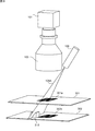
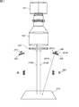
図1を参照して本発明に係わる外観検査装置の構成を説明する。外観検査装置は、検査対象210を撮像するためのCMOS又はCCDを備えた撮像カメラ101及び撮像レンズ103を有する撮像装置、断面がスリット状の照明光を生成し、検査対象210に照射する照明装置105、紫外光を生成し、検査対象210に照射する紫外光光源201、RGBの3色を含む可視光を生成し、検査対象210に照射する可視光光源203、紫外光光源201の出射側に設けられた可視光吸収フィルタ205、撮像レンズ103の入射側に設けられた可視光透過フィルタ又は紫外線カットフィルタ207を有する。撮像カメラ101からの画像データはコンピュータ212に送信される。コンピュータ212は、画像データから検査対象210の検査を行う。撮像装置の光軸は、検査対象210に垂直に配置されている。撮像カメラ101、撮像レンズ103、及び、紫外線カットフィルタ207は、撮像装置の光軸に沿って配置されている。可視光光源203、紫外光光源201、及び、可視光吸収フィルタ205は、光軸の周囲に複数個設けられてよい。照明装置105の光軸は、撮像装置の光軸に対して所定の角度傾斜している。
A configuration of an appearance inspection apparatus according to the present invention will be described with reference to FIG. The appearance inspection apparatus is an imaging apparatus having an
本発明に係わる外観検査装置は、例えば、遊技機用基板の製造ラインにおいて遊技機用基板ユニットの検査に用いることができる。しかしながら、本発明に係わる外観検査装置は、遊技機用基板ユニットと同様な構造を備えた器具の検査に適用可能である。 The appearance inspection apparatus according to the present invention can be used, for example, for inspection of a gaming machine board unit in a gaming machine board production line. However, the appearance inspection apparatus according to the present invention is applicable to inspection of equipment having a structure similar to that of a gaming machine substrate unit.
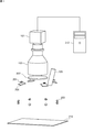
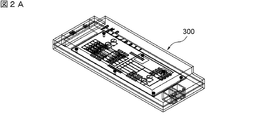
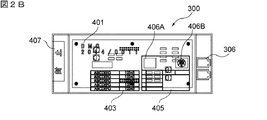
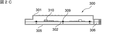
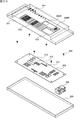
図2Aは遊技機用の基板ユニット300の外観を示す斜視図、図2Bは遊技機用の基板ユニット300の平面構成を示す図、図2Cは遊技機用の基板ユニット300の側面構成を示す図である。更に、図2Dは遊技機用の基板ユニット300の分解構造を示す。図2Dに示すように、基板ユニット300は、カバー301とボックス305とその間に収納された基板302を有する。カバー301とボックス305は、カシメ構造306又はクリップにより機械的に接合されている。基板302はネジ309によってボックス305に固定されている。基板302には、ROM等の電子部品310、311、312が実装されている。カバー301とボックス305は、内部の基板302を視認することができるように、無色の又は着色された透明な樹脂、プラスチック等によって形成されている。
2A is a perspective view showing an appearance of the
透明なカバー301には、刻印文字401が形成されている。刻印文字401は、例えば、浮き彫り状、又は、溝状の立体形状にて成形されている。刻印文字401はレーザによる刻印によって形成されてもよいが、カバーの成型時に型により形成してもよい。刻印文字401は、この基板ユニット300が適用される複数のモデルの機種及び社名を含む。透明なカバー301には、基板の電気的、動作的な説明を記載した機能シール403と基板の識別情報を記載した識別情報シール405が貼り付けられている。透明なカバー301には「検印」の印影406Bが表示されている。印影406Bは白色塗料又は白色紙で形成された白地406Aの上に表示されたものである。基板ユニット300の端部には「開封禁止」の文字が印字された封止紙407が貼り付けられている。
A stamped
遊技機用基板の製造ラインでは、(イ)カバー301の刻印文字401の有無と記載内容の確認、(ロ)(ハ)機能シール403及び識別情報シール405の有無と記載内容の確認、(ニ)カシメ構造306又はクリップの有無の確認、(ホ)白地406A上の「検印」等の印影406Bの有無の確認等を行う。本発明の第1の実施形態では、(イ)カバー301の刻印文字401の有無と記載内容の確認を行う。本発明の第2の実施形態では、(ロ)(ハ)機能シール403及び識別情報シール405の有無と記載内容の確認、(ニ)カシメ構造306又はクリップの有無の確認を行う。本発明の第3の実施形態では、(ホ)白地406A上の「検印」等の印影406Bの有無の確認等を行う。
In the production line for gaming machine substrates, (a) the presence or absence of the stamped
図3及び図4を参照して、本発明の第1の実施形態について説明する。第1の実施形態では、透明なカバー301の刻印文字401の有無確認や文字認識等の検査を行う。ここでは、検査対象として、遊技機用の基板ユニット300のカバー301を例として説明するが、検査対象となるのは、刻印文字401が形成された透明部材であればどのようなものでものよい。尚、カバー301の下側の基板302及び電子部品は非検査対象である。
A first embodiment of the present invention will be described with reference to FIGS. 3 and 4. In the first embodiment, the presence / absence check of the stamped
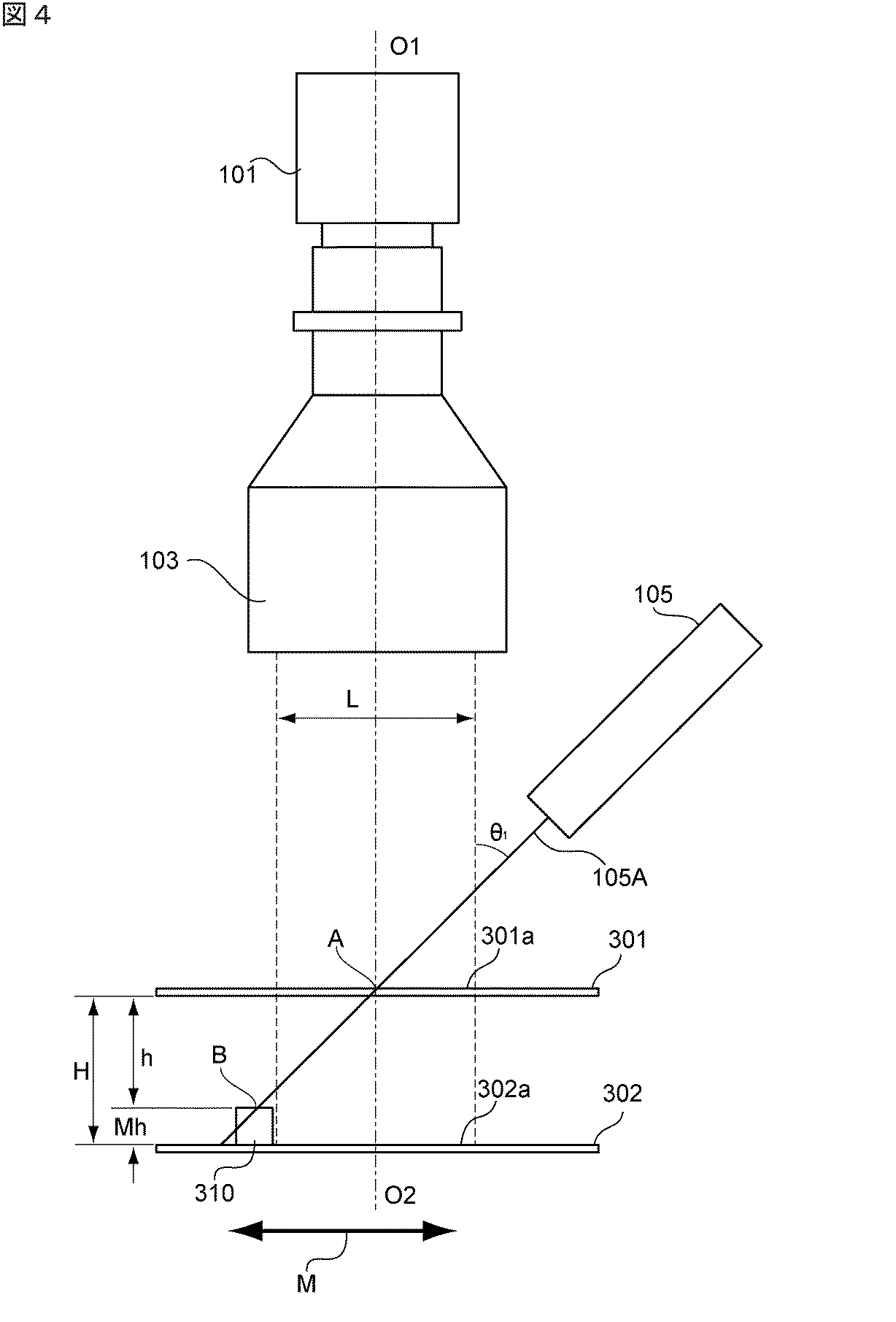
第1の実施形態では、照明装置105は、レーザ光源又はLED光源のように指向性且つ非散乱性のスリット状断面の照明光105Aを生成する。照明光105Aは、基板ユニットのカバー301を照射し、反射成分と透過成分に分かれる。透過成分は、基板302の表面や実装された電子部品310を照射する。以下に、検査対象であるカバー301を透明体301と称し、非検査対象である基板302を不透明体302と称する。更に、非検査対象である電子部品等を突起物310と称する。ここでは、撮像レンズ103は透明体301に対して上側にあり、不透明体302は透明体301に対して下側にあるとする。
In the first embodiment, the
本実施形態では、照明光105Aの光軸は、撮像レンズ103の光軸(O1−O2)に対して、所定の傾斜角θ1だけ傾斜している。そのため、照明光105Aは、透明体301の撮像領域301aを照射するが、透過した照明光は、不透明体302の撮像領域302aの外側を照射する。従って、撮像カメラ101は、透明体301の表面の撮像領域301aを反射した成分のみを撮像し、不透明体302からの反射光は撮像しない。即ち、撮像カメラ101は、透明体301の撮像領域301aにおける検査対象のみを撮像し、非検査対象である不透明体302を撮像しない。
In the present embodiment, the optical axis of the
照明光105Aは細いスリット状断面を有する。従って、検査対象である透明体301の全体の画像を得るためには、透明体301を移動させてスキャン画像を取得する必要がある。本実施形態では、透明体301及び不透明体302は、撮像レンズ103の光軸(O1−O2)に対して直交する面に沿って移動するように構成されている。撮像カメラ101によって得られたスキャン画像から、検査対象である透明体301の全体の画像を生成することができる。尚、スキャン画像より、透明体301の上面301Aに形成された刻印文字の領域の画像を順に取り出し、各領域の画像の明るさから、凹凸による反射率の変化を判定し、刻印文字の有無又は良否を判定してもよい。例えば、刻印文字の領域の画像の明るさを標準値と比較してもよく、又は、製造ラインで順次送られてくる透明体の明るさを前後の透明体の明るさと比較してもよい。更に、検査のパラメータとして、刻印文字の領域の画像の明るさばかりでなく、画像認識によって抽出した画像の特徴を用いてもよい。
The
図5を参照して、照明光105Aによって、検査対象である透明体301の撮像領域301aのみを照射し、非検査対象である不透明体302の撮像領域302aを照射しないための条件を求める。線O1−O2は撮像装置の光軸を表す。線D1、D2は、撮像領域301a及び302aの両側の縁の位置を示す。透明体301の上面301Aと下面301Bは、互いに平行であり、光軸O1−O2に対して垂直であるとする。また、照明光105Aの断面は細いスリット状であるが、その短手側の幅を0とする。透明体301の上の空間321の光の屈折率をn1、透明体301の光の屈折率をn2、透明体301と不透明体302の間の空間322の光の屈折率をn3とする。透明体301の上面301Aにおける照明光105Aの入射点をA、透明体301の下面301Bにおける照明光105Aの出射点をC、突起物310の上面における照明光105Aの入射点をBとする。
Referring to FIG. 5, a condition for irradiating
図示の例では、点Aは、光軸O1−O2上にあるが、必ずしも光軸O1−O2上にあるとは限らない。点Aは、透明体301の表面の撮像領域301aにあればよい。点Aは、照明装置105の取付け角度又は取付け位置によって変化する。点Aにおける照明光105Aの入射角をθ1、点Cにおける照明光105Aの出射角をθ2、点Bにおける照明光105Aの入射角をθ3とする。ここで入射角は、法線、即ち、光軸O1−O2と照明光105Aのなす角とする。
In the illustrated example, the point A is on the optical axis O1-O2, but is not necessarily on the optical axis O1-O2. The point A may be in the
点Aと点Cの間の水平距離をx1、点Bと点Cの間の水平距離をx2、点Aから線D1までの距離をLA、撮像領域301a及び302aの両縁の間の距離をLとする。更に、透明体301の厚さをT、空間322の厚さをH、突起物310の高さをMh、突起物310の上面と透明体301の下面301Bの間の距離をhとする。距離hは、透明体301と不透明体302の間の最短距離とする。点Bが、不透明体302の表面の撮像領域302aより外側にある条件は次の式によって表される。
The horizontal distance between the point A and the point C is x1, the horizontal distance between the point B and the point C is x2, the distance from the point A to the line D1 is LA, and the distance between both edges of the
上述の条件は、透明体301の上の空間321、透明体301、透明体301と不透明体302の間の空間322の3つの層を有する場合について当てはまる。しかしながら、上式は、2つの層の場合にも適合する。例えば、透明体301の厚さT=0とすることにより、2つの層の場合となる。また、例えば、突起物が存在せずかつ不透明体302の上面302Aに印刷された文字等が存在し、透明体301が不透明体302の上面302Aに接触している場合、h=0とすることにより、2つの層の場合となる。
The above-mentioned condition is applied to the case where the three layers of the
撮像領域301aの幅Lの調整は、撮像レンズ103の取り込み径や、カメラセンサ上の撮像領域の設定によって可変である。点Aにおける照明光105Aの断面の短手側の幅は十分に小さいため、図5のスキャン方向Mへのスキャン動作により、検査対象である透明体301を連続的に撮像する。
The adjustment of the width L of the
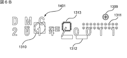
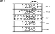
図6Aは、第1の実施形態の外観検査装置によって得られた画像の例を示す。この画像には、透明なカバー301の刻印文字の像1401が現れているが、基板302の電子部品等の像は現れていない。即ち、検査対象の像のみを含み非検査対象の像を含まない画像が得られる。従って、検査対象である刻印文字401の有無、良否の認識を正確に行うことができる。図6Bは、通常の撮像装置によって得られたた画像の例を示す。この画像には、透明なカバー301の刻印文字の像1401ばかりでなく、下側の基板302の電子部品の像1310、1311、1312、1313及びネジの像1309が現れている。即ち、検査対象の像ばかりでなく非検査対象の像も含む画像が得られる。従って、検査対象である刻印文字401の有無、良否の認識を正確に行うことができない。
FIG. 6A shows an example of an image obtained by the appearance inspection apparatus of the first embodiment. In this image, an
ここでは、検査対象として、透明なカバー301に形成された刻印文字の場合を説明したが、検査対象はこれに限定されるわけではない。検査対象は、例えば、透明体の表面に施された印刷等であってもよく、透明体の表面のキズやくもり等であってもよい。
Here, the case of the stamped character formed on the
図7を参照して本発明の第2の実施形態を説明する。第2の実施形態では、透明なカバー301の機能シール403の有無と記載内容の確認、識別情報シール405の有無と記載内容の確認、カシメ構造306又はクリップの有無確認、等の検査を行う。以下に、検査対象として、透明なカバー301の機能シール403を例として説明する。尚、ここでは、検査対象として、遊技機用の基板ユニット300のカバー301を例として説明するが、検査対象となるのは、同様な透明部材であればどのようなものでものよい。尚、カバー301の下側の基板302及び電子部品は非検査対象である。
A second embodiment of the present invention will be described with reference to FIG. In the second embodiment, inspections such as the presence / absence and description of the
本実施形態では、検査対象である機能シール403は、紫外線を受光すると励起による可視光線を生成する物質、又は、材料を含む。このような物質として、例えば、紫外光励起蛍光が知られている。従って、検査対象に紫外光が照射されると、蛍光可視光が生成される。一方、非検査対象である基板302及び電子部品は、このような材料を含まない。非検査対象に紫外光が照射されても、蛍光可視光は生成されない。
In the present embodiment, the
通常、紫外光光源201は、紫外光201Aを生成するが、同時に、僅かであるが可視光201Bを生成する。紫外光光源201の出射側に設けられた可視光吸収フィルタ205は可視光201Bを吸収し、紫外光201Aを透過させる。可視光吸収フィルタ205を透過した紫外光201Aのみが、検査対象210に照射される。この紫外光201Aは非検査対象(図示なし)にも照射される。
Normally, the ultraviolet
検査対象210からは、蛍光である可視光210Aが生成されると同時に、非検査対象からは、反射光である紫外光210Bが生成される。検査対象210からの蛍光可視光210Aと、非検査対象からの反射紫外光210Bは、紫外線カットフィルタ207に到達する。蛍光可視光210Aは紫外線カットフィルタ207を透過し、反射紫外光210Bは紫外線カットフィルタ207によって吸収される。紫外線カットフィルタ207を透過した蛍光可視光210Aは、撮像レンズ103を経由して、可視光撮像カメラ101によって受光される。こうして、検査対象210のみが撮像され、非検査対象が撮像されていない画像が得られる。
From the
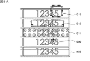
図8Aは、照明装置として可視光光源203を用い、可視光吸収フィルタ205及び紫外線カットフィルタ207を用いない場合の可視光撮像カメラ101による画像の例である。図示のように、検査対象である機能シール403の像1403ばかりでなく、非検査対象である基板302に実装された電子部品の像1311、1312、1313及びネジの像1309が現れている。基板302及び電子部品は光の反射率が高く、また、ネジ309等の金属も光の反射率が高い。そのため、これらの非検査対象の像が現れ、検査対象の識別が困難となる。
FIG. 8A is an example of an image obtained by the visible
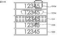
図8Bは、照明装置として紫外光光源201を用い、可視光吸収フィルタ205及び紫外線カットフィルタ207を用いない場合の可視光撮像カメラ101による画像の例である。紫外光光源201は紫外光を生成するが、僅かであるが可視光を生成する。従って、検査対象によって、蛍光可視光及び可視光の反射光が生成される。非検査対象によって、可視光及び紫外光の反射光が生成される。可視光撮像カメラ101は、検査対象からの蛍光可視光及び反射可視光と非検査対象からの反射可視光及び反射紫外光を受光する。そのため、図示のように、検査対象である機能シール403の像1403ばかりでなく、非検査対象である基板302に実装された電子部品の像1311、1312a、1313a及びネジの像1309が現れている。
FIG. 8B is an example of an image obtained by the visible
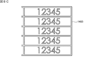
図8Cは本実施形態による外観検査装置による検査対象210の画像の例を示す。本実施形態では、照明装置として紫外光光源201を用い、可視光吸収フィルタ205及び紫外線カットフィルタ207を用いる。本実施形態では、可視光吸収フィルタ205を用いるため、検査対象及び非検査対象に紫外光のみが照射される。検査対象によって、蛍光可視光のみが生成され、非検査対象によって、反射紫外光のみが生成される。一方、紫外線カットフィルタ207を用いるため、可視光撮像カメラ101は、検査対象からの蛍光可視光のみを受光する。検査対象である機能シール403の像1403のみが現れ、非検査対象である基板302に実装された電子部品の像1311、1312、1313及びネジの像1309が現れていない。
FIG. 8C shows an example of an image of the
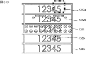
図8Dは、照明装置として紫外光光源201を用い、可視光吸収フィルタ205を用いるが、紫外線カットフィルタ207を用いない場合の可視光撮像カメラ101による画像の例である。本実施形態では、可視光吸収フィルタ205を用いるため、検査対象及び非検査対象に紫外光のみが照射される。検査対象によって、蛍光可視光のみが生成され、非検査対象によって、反射紫外光のみが生成される。しかしながら、紫外線カットフィルタ207を用いないため、可視光撮像カメラ101は、検査対象からの蛍光可視光と非検査対象からの反射紫外光を受光する。この反射紫外光は、可視光撮像カメラ101に外乱として受光される。従って、可視光撮像カメラ101による可視光像は、紫外光による外乱の影響を受ける。従って、検査対象である機能シール403の像1403ばかりでなく、非検査対象である基板302に実装された電子部品の像1311、1312b、1313a及びネジの像1309が現れている。
FIG. 8D is an example of an image obtained by the visible
図8Eは、照明装置として紫外光光源201を用い、可視光吸収フィルタ205を用いないが、紫外線カットフィルタ207を用いる場合の可視光撮像カメラ101による画像の例である。本実施形態では、可視光吸収フィルタ205を用いないため、検査対象及び非検査対象に紫外光及び可視光が照射される。検査対象によって、蛍光可視光が生成されるが、非検査対象によって、可視光及び紫外光の反射光が生成される。しかしながら、紫外線カットフィルタ207を用いるため、可視光撮像カメラ101は、検査対象からの蛍光可視光と非検査対象からの反射可視光を受光する。従って、検査対象である機能シール403の像1403ばかりでなく、非検査対象である基板302に実装された電子部品の像1311、1312b、1313a及びネジの像1309が現れている。
FIG. 8E is an example of an image obtained by the visible
ここでは、検査対象210は、紫外光を照射すると可視光を励起する物質又は材料を含むように構成されている。しかしながら、検査対象210は、例えば、赤外線を照射すると可視光を励起する物質又は材料を含むように構成してもよい。この場合には、紫外光光源201の代わりに赤外線光源を用い、紫外線カットフィルタ207の代わりに赤外線カットフィルタを用いるとよい。検査対象210は、例えば、紫外光を照射すると可視光を励起する物質又は材料を含む紙又はテープであってもよい。更に、検査対象210は、可視光を照射すると励起する、物質又は材料を含むように構成してもよい。
Here, the
本発明の第2の実施形態において、検査対象を様々な分野で選択することが可能である。例えば、紫外線又は赤外線で励起する塗料又はテープを有価証券や紙幣等に塗布したものを検査対象とすることができる。更に、蛍光試薬を用いた試料を検査対象とし、それを顕微鏡観察してもよい。この場合、紫外光、可視光、又は赤外光を励起用光線として用い、蛍光可視光を顕微鏡観察する。紫外線カットフィルタ207の代わりに蛍光波長のみを透過するフィルタを用い、可視光吸収フィルタ205の代わりに励起用光のみを透過させるフィルタを用いる。このような蛍光試薬として、フローサイトメトリーで使用される蛍光色素が知られている。
In the second embodiment of the present invention, it is possible to select an inspection object in various fields. For example, a coating or a tape that is excited by ultraviolet rays or infrared rays and applied to securities, banknotes, or the like can be an inspection target. Furthermore, a sample using a fluorescent reagent may be used as an inspection target and observed with a microscope. In this case, ultraviolet light, visible light, or infrared light is used as an excitation light beam, and fluorescence visible light is observed with a microscope. A filter that transmits only the fluorescence wavelength is used instead of the
図9、図10A及び図10Bを参照して、本発明の第3の実施形態を説明する。第3の実施形態では、透明なカバー301に付された「検印」等の印影406Bの有無を確認する検査を行う。印影406Bは着色されており白地406Aの上に形成される。ここでは、検査対象として、遊技機用の基板ユニット300のカバー301を例として説明するが、検査対象となるのは、基板ユニット300のカバー301に限定されない。
A third embodiment of the present invention will be described with reference to FIGS. 9, 10A and 10B. In the third embodiment, an inspection for confirming the presence / absence of a
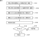
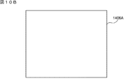
本実施形態では、可視光光源203は印影406Bの色と同一の色の照明光と、異なる色の照明光を生成するように構成されている。先ず、ステップS101にて、可視光光源203より印影406Bと同色の照明光を生成し、検査対象である透明なカバー301に付された印影406Bに照射する。次に、可視光撮像カメラ101によって画像1を取得する。図10Bは画像1の例を示す。印影406Bと同一色の照明光によって撮像すると、無地の白色1406Aの画像が得られる。
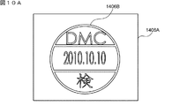
In the present embodiment, the visible
ステップS102にて、可視光光源203より印影406Bと異なる色の照明光を生成し、検査対象である透明なカバー301に付された印影406Bに照射する。次に、可視光撮像カメラ101によって画像2を取得する。図10Aは画像2の例を示す。印影406Bと異なる色の照明光によって撮像すると、無地の白色1406Aに着色した印影の像1406Bの画像が得られる。ステップ103にて、画像1を構成する画素を黒と白に2値化し、白の画素数W1を計数する。ステップ104にて、画像2を構成する画素を黒と白に2値化し、白の画素数W2を計数する。ステップ105にて、判定値Xを設定する。ステップ106にて、画素数の差W1−W2が判定値Xより大きいか否かを判定する。尚、画像1と画像2の寸法は同一であるとする。即ち、画像1の総画素数と画像2の総画素数は同一であるとする。
In step S102, illumination light having a color different from that of the
ステップ106にて大きいと判定された場合には、ステップS107に進み、印影が良好であると判定する。ステップ106にて小さいか又は等しい大きいと判定された場合には、ステップS108に進み、印影が不良であると判定する。ここで、ステップ105における判定値Xの設定方法の例を説明する。予め多数の良好な印影について、画素数の差W1−W2を求め、その平均値、又は、下限値を判定値Xとしてよい。
If it is determined in step 106 that it is large, the process proceeds to step S107, and it is determined that the seal is good. If it is determined in step 106 that it is small or equal and large, the process proceeds to step S108, where it is determined that the seal is defective. Here, an example of a method for setting the determination value X in
以上、本発明の実施の形態を説明したが、本発明の範囲はこれらの実施の形態によって制限されるものではなく、特許請求の範囲に記載された発明の範囲にて様々な変更が可能であることは当業者であれば容易に理解されよう。 Although the embodiments of the present invention have been described above, the scope of the present invention is not limited by these embodiments, and various modifications can be made within the scope of the invention described in the claims. This will be readily appreciated by those skilled in the art.
101…撮像カメラ、103…撮像レンズ、105…照明装置、201…紫外光光源、203…可視光光源、205…可視光吸収フィルタ、207…紫外線カットフィルタ、210…検査対象、212…コンピュータ、300…基板ユニット、301…カバー(透明体)、302…基板(不透明体)、305…ボックス、306…カシメ部又はクリップ、309…ネジ、310、311、312…電子部品(突起物)、401…刻印文字、403…機能シール、405…識別情報シール、406A…白地、406B…印影、407…封止紙
DESCRIPTION OF
Claims (2)
前記照明装置は指向性且つ非散乱性のスリット状断面の照明光を生成し、前記照明装置の光軸は、前記撮像装置の光軸に対して傾斜しており、
前記照明装置からの照明光は、前記透明体における撮像領域を照射するが、前記透明体を透過した照明光は前記不透明体における撮像領域の外側を照射し、
前記撮像装置は、前記透明体の検査対象からの反射光のみを受光することによって、前記透明体の検査対象のみを撮像し、前記検査対象のスキャン画像を生成することを特徴とする外観検査装置。 In an appearance inspection apparatus having an illumination device that irradiates illumination light to a container unit made of an opaque body and a transparent body that covers the opaque body, and an imaging device for imaging an inspection object formed on the transparent body,
The illumination device generates directional and non-scattering slit-shaped illumination light, and the optical axis of the illumination device is inclined with respect to the optical axis of the imaging device,
The illumination light from the illumination device irradiates the imaging area in the transparent body, but the illumination light transmitted through the transparent body irradiates the outside of the imaging area in the opaque body,
The imaging apparatus receives only the reflected light from the inspection object of the transparent body, captures only the inspection object of the transparent body, and generates a scan image of the inspection object. .
前記容器ユニットは遊技機用の基板と該基板を覆う透明なカバーを有する遊技機用の基板ユニットであり、前記検査対象は前記透明なカバーに形成された刻印文字であることを特徴とする外観検査装置。 The container unit is a gaming machine board unit having a gaming machine board and a transparent cover covering the board, and the inspection object is a stamped character formed on the transparent cover. Inspection device.
Priority Applications (1)
| Application Number | Priority Date | Filing Date | Title |
|---|---|---|---|
| JP2015057017A JP6564591B2 (en) | 2015-03-20 | 2015-03-20 | Appearance inspection apparatus, appearance inspection method, and substrate unit |
Applications Claiming Priority (1)
| Application Number | Priority Date | Filing Date | Title |
|---|---|---|---|
| JP2015057017A JP6564591B2 (en) | 2015-03-20 | 2015-03-20 | Appearance inspection apparatus, appearance inspection method, and substrate unit |
Publications (2)
| Publication Number | Publication Date |
|---|---|
| JP2016174725A JP2016174725A (en) | 2016-10-06 |
| JP6564591B2 true JP6564591B2 (en) | 2019-08-21 |
Family
ID=57070639
Family Applications (1)
| Application Number | Title | Priority Date | Filing Date |
|---|---|---|---|
| JP2015057017A Expired - Fee Related JP6564591B2 (en) | 2015-03-20 | 2015-03-20 | Appearance inspection apparatus, appearance inspection method, and substrate unit |
Country Status (1)
| Country | Link |
|---|---|
| JP (1) | JP6564591B2 (en) |
Family Cites Families (9)
| Publication number | Priority date | Publication date | Assignee | Title |
|---|---|---|---|---|
| JPH08241374A (en) * | 1995-03-02 | 1996-09-17 | Canon Inc | Character reading device and method |
| JPH09147092A (en) * | 1995-11-24 | 1997-06-06 | Dainippon Printing Co Ltd | Inspection device |
| JPH1190011A (en) * | 1997-09-16 | 1999-04-06 | Sankyo Kk | Board box of game machine |
| JP2003263627A (en) * | 2002-03-08 | 2003-09-19 | Olympus Optical Co Ltd | Image taking-in device |
| JP4650830B2 (en) * | 2005-04-18 | 2011-03-16 | サミー株式会社 | Board case for gaming machine and gaming machine equipped with the same |
| JP2006334272A (en) * | 2005-06-06 | 2006-12-14 | Samii Kk | Inspecting apparatus of board assembly |
| JP4822349B2 (en) * | 2006-12-26 | 2011-11-24 | サミー株式会社 | Game machine fraud prevention device |
| JP5064913B2 (en) * | 2007-07-05 | 2012-10-31 | 株式会社藤商事 | Inspection method and equipment for manufacturing play boards |
| JP5995600B2 (en) * | 2012-08-08 | 2016-09-21 | 株式会社藤商事 | Play board inspection device and inspection method |
-
2015
- 2015-03-20 JP JP2015057017A patent/JP6564591B2/en not_active Expired - Fee Related
Also Published As
| Publication number | Publication date |
|---|---|
| JP2016174725A (en) | 2016-10-06 |
Similar Documents
| Publication | Publication Date | Title |
|---|---|---|
| US8345249B2 (en) | Liquid sample analyzing method | |
| KR100828981B1 (en) | Method and apparatus for inspecting front surface shape | |
| CN109313133B (en) | Surface inspection system and surface inspection method | |
| CN102971744B (en) | Method and device for measuring optical properties of an optically variable marking applied to an object | |
| RU2598296C2 (en) | Method for checking optical security feature of value document | |
| US20080316476A1 (en) | System and Device for the Optical Inspection of Glass Panels | |
| CN107735675B (en) | Substrate inspection device and substrate manufacturing method | |
| US9897555B2 (en) | Defect inspection method and apparatus therefor | |
| KR101595581B1 (en) | An Optical Device for Observing Millimetric or Submillimetric Structural Details of an Object with Specular Behaviour | |
| JP5776949B2 (en) | Inspection method | |
| KR20190041009A (en) | Inspection device, inspection method and program | |
| JP7039700B2 (en) | Inspection device with light watermark | |
| JP4151306B2 (en) | Inspection method of inspection object | |
| JP2020529618A5 (en) | ||
| JP6564591B2 (en) | Appearance inspection apparatus, appearance inspection method, and substrate unit | |
| KR100517868B1 (en) | Method for determining and evaluating defects in a sample surface | |
| JP2001056297A (en) | Surface inspection method and device therefor | |
| JP4910128B2 (en) | Defect inspection method for object surface | |
| US12301770B2 (en) | Information processing apparatus, abnormality detection method, storage medium, and information processing system | |
| KR102868765B1 (en) | Method for inspecting mini led mounting | |
| JP2020091132A (en) | Surface defect inspection device of translucent member | |
| JP4967132B2 (en) | Defect inspection method for object surface | |
| KR20230067759A (en) | optical inspection device and inspecting method using the same | |
| JP2022170295A (en) | ELECTRONIC DEVICE, DISPLAY, AND INFORMATION READING METHOD OF ELECTRONIC DEVICE | |
| EP4610632A1 (en) | Measurement apparatus and measurement method |
Legal Events
| Date | Code | Title | Description |
|---|---|---|---|
| A621 | Written request for application examination |
Free format text: JAPANESE INTERMEDIATE CODE: A621 Effective date: 20180202 |
|
| A977 | Report on retrieval |
Free format text: JAPANESE INTERMEDIATE CODE: A971007 Effective date: 20181019 |
|
| A131 | Notification of reasons for refusal |
Free format text: JAPANESE INTERMEDIATE CODE: A131 Effective date: 20181127 |
|
| A521 | Request for written amendment filed |
Free format text: JAPANESE INTERMEDIATE CODE: A523 Effective date: 20190117 |
|
| TRDD | Decision of grant or rejection written | ||
| A01 | Written decision to grant a patent or to grant a registration (utility model) |
Free format text: JAPANESE INTERMEDIATE CODE: A01 Effective date: 20190702 |
|
| A61 | First payment of annual fees (during grant procedure) |
Free format text: JAPANESE INTERMEDIATE CODE: A61 Effective date: 20190729 |
|
| R150 | Certificate of patent or registration of utility model |
Ref document number: 6564591 Country of ref document: JP Free format text: JAPANESE INTERMEDIATE CODE: R150 |
|
| LAPS | Cancellation because of no payment of annual fees |