JP6552383B2 - Automated TEM sample preparation - Google Patents
Automated TEM sample preparation Download PDFInfo
- Publication number
- JP6552383B2 JP6552383B2 JP2015215353A JP2015215353A JP6552383B2 JP 6552383 B2 JP6552383 B2 JP 6552383B2 JP 2015215353 A JP2015215353 A JP 2015215353A JP 2015215353 A JP2015215353 A JP 2015215353A JP 6552383 B2 JP6552383 B2 JP 6552383B2
- Authority
- JP
- Japan
- Prior art keywords
- probe
- sample
- image
- tip
- charged particle
- Prior art date
- Legal status (The legal status is an assumption and is not a legal conclusion. Google has not performed a legal analysis and makes no representation as to the accuracy of the status listed.)
- Active
Links
- 0 *CC1C*CCC1 Chemical compound *CC1C*CCC1 0.000 description 1
Images


Classifications
-
- H—ELECTRICITY
- H01—ELECTRIC ELEMENTS
- H01J—ELECTRIC DISCHARGE TUBES OR DISCHARGE LAMPS
- H01J37/00—Discharge tubes with provision for introducing objects or material to be exposed to the discharge, e.g. for the purpose of examination or processing thereof
- H01J37/30—Electron-beam or ion-beam tubes for localised treatment of objects
- H01J37/302—Controlling tubes by external information, e.g. programme control
- H01J37/3023—Programme control
-
- G—PHYSICS
- G01—MEASURING; TESTING
- G01N—INVESTIGATING OR ANALYSING MATERIALS BY DETERMINING THEIR CHEMICAL OR PHYSICAL PROPERTIES
- G01N1/00—Sampling; Preparing specimens for investigation
- G01N1/28—Preparing specimens for investigation including physical details of (bio-)chemical methods covered elsewhere, e.g. G01N33/50, C12Q
- G01N1/286—Preparing specimens for investigation including physical details of (bio-)chemical methods covered elsewhere, e.g. G01N33/50, C12Q involving mechanical work, e.g. chopping, disintegrating, compacting, homogenising
-
- H—ELECTRICITY
- H01—ELECTRIC ELEMENTS
- H01J—ELECTRIC DISCHARGE TUBES OR DISCHARGE LAMPS
- H01J37/00—Discharge tubes with provision for introducing objects or material to be exposed to the discharge, e.g. for the purpose of examination or processing thereof
- H01J37/26—Electron or ion microscopes; Electron or ion diffraction tubes
- H01J37/28—Electron or ion microscopes; Electron or ion diffraction tubes with scanning beams
-
- H—ELECTRICITY
- H01—ELECTRIC ELEMENTS
- H01J—ELECTRIC DISCHARGE TUBES OR DISCHARGE LAMPS
- H01J37/00—Discharge tubes with provision for introducing objects or material to be exposed to the discharge, e.g. for the purpose of examination or processing thereof
- H01J37/26—Electron or ion microscopes; Electron or ion diffraction tubes
- H01J37/285—Emission microscopes, e.g. field-emission microscopes
-
- H—ELECTRICITY
- H01—ELECTRIC ELEMENTS
- H01J—ELECTRIC DISCHARGE TUBES OR DISCHARGE LAMPS
- H01J37/00—Discharge tubes with provision for introducing objects or material to be exposed to the discharge, e.g. for the purpose of examination or processing thereof
- H01J37/30—Electron-beam or ion-beam tubes for localised treatment of objects
- H01J37/304—Controlling tubes by information coming from the objects or from the beam, e.g. correction signals
- H01J37/3045—Object or beam position registration
-
- H—ELECTRICITY
- H01—ELECTRIC ELEMENTS
- H01J—ELECTRIC DISCHARGE TUBES OR DISCHARGE LAMPS
- H01J37/00—Discharge tubes with provision for introducing objects or material to be exposed to the discharge, e.g. for the purpose of examination or processing thereof
- H01J37/30—Electron-beam or ion-beam tubes for localised treatment of objects
- H01J37/31—Electron-beam or ion-beam tubes for localised treatment of objects for cutting or drilling
-
- G—PHYSICS
- G01—MEASURING; TESTING
- G01N—INVESTIGATING OR ANALYSING MATERIALS BY DETERMINING THEIR CHEMICAL OR PHYSICAL PROPERTIES
- G01N1/00—Sampling; Preparing specimens for investigation
- G01N1/28—Preparing specimens for investigation including physical details of (bio-)chemical methods covered elsewhere, e.g. G01N33/50, C12Q
- G01N1/286—Preparing specimens for investigation including physical details of (bio-)chemical methods covered elsewhere, e.g. G01N33/50, C12Q involving mechanical work, e.g. chopping, disintegrating, compacting, homogenising
- G01N2001/2873—Cutting or cleaving
-
- H—ELECTRICITY
- H01—ELECTRIC ELEMENTS
- H01J—ELECTRIC DISCHARGE TUBES OR DISCHARGE LAMPS
- H01J2237/00—Discharge tubes exposing object to beam, e.g. for analysis treatment, etching, imaging
- H01J2237/20—Positioning, supporting, modifying or maintaining the physical state of objects being observed or treated
- H01J2237/208—Elements or methods for movement independent of sample stage for influencing or moving or contacting or transferring the sample or parts thereof, e.g. prober needles or transfer needles in FIB/SEM systems
-
- H—ELECTRICITY
- H01—ELECTRIC ELEMENTS
- H01J—ELECTRIC DISCHARGE TUBES OR DISCHARGE LAMPS
- H01J2237/00—Discharge tubes exposing object to beam, e.g. for analysis treatment, etching, imaging
- H01J2237/30—Electron or ion beam tubes for processing objects
- H01J2237/317—Processing objects on a microscale
- H01J2237/3174—Etching microareas
- H01J2237/31745—Etching microareas for preparing specimen to be viewed in microscopes or analyzed in microanalysers
Landscapes
- Chemical & Material Sciences (AREA)
- Analytical Chemistry (AREA)
- Physics & Mathematics (AREA)
- Health & Medical Sciences (AREA)
- Life Sciences & Earth Sciences (AREA)
- Biochemistry (AREA)
- General Health & Medical Sciences (AREA)
- General Physics & Mathematics (AREA)
- Immunology (AREA)
- Pathology (AREA)
- Engineering & Computer Science (AREA)
- Plasma & Fusion (AREA)
- Sampling And Sample Adjustment (AREA)
- Analysing Materials By The Use Of Radiation (AREA)
- Drying Of Semiconductors (AREA)
- Testing Or Measuring Of Semiconductors Or The Like (AREA)
Description
本発明は、荷電粒子ビーム・システムで観察するための試料の自動化された調製に関する。 The present invention relates to the automated preparation of samples for observation in charged particle beam systems.
半導体回路製造法ならびに他のマイクロスコピックおよびナノスコピック製造技法は、改良された分解能を有する新しい画像化技法の開発を必要としている。改良された画像化技法は生命科学でも必要とされている。電子顕微鏡法、イオン顕微鏡法などの荷電粒子ビーム顕微鏡法は、光学顕微鏡法よりもかなり高い分解能および大きな焦点深度を提供する。走査電子顕微鏡(SEM)では、1次電子ビームを微小なスポットに集束させ、観察しようとする表面をそのスポットで走査する。表面に1次電子ビームが衝突すると、その表面から2次電子が放出される。その2次電子を検出し、画像を形成する。このとき、画像のそれぞれの点の輝度は、その表面の対応するスポットにビームが衝突したときに検出された2次電子の数によって決定される。SEMは、2次電子の代替として後方散乱電子からも画像を形成することができる。走査イオン顕微鏡法(SIM)は、走査電子顕微鏡法と似ているが、表面を走査し、2次電子を放出させる目的にイオン・ビームを使用する。イオン顕微鏡は、2次イオンを使用して画像を形成することもできる。 Semiconductor circuit fabrication methods and other microscopic and nanoscopic fabrication techniques require the development of new imaging techniques with improved resolution. Improved imaging techniques are also needed in life sciences. Charged particle beam microscopy, such as electron microscopy, ion microscopy, provides much higher resolution and greater depth of focus than optical microscopy. In a scanning electron microscope (SEM), a primary electron beam is focused on a minute spot, and the surface to be observed is scanned with the spot. When a primary electron beam collides with a surface, secondary electrons are emitted from the surface. The secondary electrons are detected and an image is formed. The intensity of each point of the image is then determined by the number of secondary electrons detected when the beam strikes the corresponding spot on that surface. The SEM can also form an image from backscattered electrons as an alternative to secondary electrons. Scanning ion microscopy (SIM) is similar to scanning electron microscopy, but uses an ion beam to scan the surface and emit secondary electrons. Ion microscopes can also use secondary ions to form images.
透過電子顕微鏡(TEM)では、幅の広い電子ビームが試料に衝突し、試料を透過した電子を集束させて試料の画像を形成する。1次ビーム中の電子の多くが試料を透過し、反対側から出てくることを可能にするため、試料は十分に薄くなければならない。試料の厚さは通常200nm未満であるが、それよりもずっと薄いこともしばしばである。 In a transmission electron microscope (TEM), a broad electron beam strikes a sample and focuses the electrons transmitted through the sample to form an image of the sample. The sample must be sufficiently thin to allow much of the electrons in the primary beam to pass through the sample and out the opposite side. The thickness of the sample is usually less than 200 nm, but often much thinner.
走査透過電子顕微鏡(STEM)では、1次電子ビームを微小なスポットに集束させ、そのスポットで試料表面を走査する。加工物を透過した電子を、試料の向こう側に置かれた電子検出器によって集める。画像のそれぞれの点の強度は、その表面の対応する点に1次ビームが衝突したときに集められた電子の数に対応する。本明細書で使用する用語「TEM試料」はTEMまたはSTEM用の試料を指し、TEM用の試料を調製すると言うときには、STEMで観察するための試料を調製することも含まれると理解される。 In scanning transmission electron microscopy (STEM), a primary electron beam is focused to a minute spot and the spot scans the sample surface. Electrons that have passed through the workpiece are collected by an electron detector placed across the sample. The intensity of each point in the image corresponds to the number of electrons collected when the primary beam collides with the corresponding point on the surface. The term "TEM sample" as used herein refers to a sample for TEM or STEM, and when referring to preparing a sample for TEM, it is understood to include preparing a sample for observation with STEM.
TEM試料は非常に薄いため、試料の調製は、繊細で時間のかかる作業となる。薄い試料、特に厚さ100nm未満の試料の厚さに変動があると、試料が曲がったり、過剰にミリング(milling)してしまったり、または他の致命的な欠陥が生じたりすることがある。調製技法が、構造の特性評価の質、および最も小さく最も決定的な構造体の分析能力を決定する。 Because TEM samples are so thin, sample preparation is a delicate and time-consuming task. Variations in the thickness of thin samples, particularly samples less than 100 nm thick, can cause the sample to bend, over-mill, or cause other fatal defects. Preparation techniques determine the quality of structural characterization and the ability to analyze the smallest and most definitive structures.
加工物上で試料がどのような向きにあるかによって、TEM試料を、「断面視(cross−sectional view)」試料または「平面視(planar view)」試料に大まかに分類することができる。試料の観察しようとする面が加工物の表面に対して平行である場合、その試料は「平面視」試料と呼ばれる。観察しようとする面が加工物表面に対して直角である場合、その試料は「断面視」試料と呼ばれる。 Depending on the orientation of the sample on the workpiece, a TEM sample can be roughly classified into a “cross-section view” sample or a “planar view” sample. If the face to be observed of the sample is parallel to the surface of the workpiece, the sample is called a "planar view" sample. If the plane to be observed is perpendicular to the workpiece surface, the sample is called a "cross-sectional" sample.
TEM試料を調製するいくつかの技法が知られている。いくつかの技法は、クリービング(cleaving)、化学研磨、機械研磨、またはブロード・ビーム低エネルギー・イオン・ミリング(broad beam low energy ion milling)を含むことができる。これらの技法の組合せも可能である。これらの方法は、出発材料を次第に小さな材料片に切断していくことをしばしば必要とし、それによって原試料の多くの部分が破壊されるため、不利である。これらの方法は一般に、特定の部位だけを処理する(site specific)のではない。 Several techniques for preparing TEM samples are known. Some techniques can include cleaving, chemical polishing, mechanical polishing, or broad beam low energy ion milling. Combinations of these techniques are also possible. These methods are disadvantageous because they often require starting material to be progressively cut into smaller pieces of material, which destroys many portions of the original sample. These methods are generally not site specific of specific sites.
「リフトアウト(lift−out)」手順と一般に呼ばれている他の技法は、集束イオン・ビーム(FIB)を使用して基板から試料を切り出し、その間、基板の周囲のエリアに対する損傷を大幅に限定しまたは排除する。この技法は、例えば半導体製造の結果を分析するのに役立つ。リフトアウト技法を使用して、断面視、平面視など、任意の向きに試料を分析することができる。いくつかの技法は、追加の調製なしでTEMにおいて使用することができる十分な薄さの試料を抜き取る。他の技法では、抜き取った試料を、観察する前にさらに薄くする。 Another technique, commonly referred to as the "lift-out" procedure, uses a focused ion beam (FIB) to cut out the sample from the substrate while significantly damaging the damage to the area around the substrate. Limit or eliminate. This technique is useful, for example, to analyze the results of semiconductor manufacturing. The lift-out technique can be used to analyze the sample in any orientation, such as cross-sectional view, planar view, and the like. Some techniques remove sufficiently thin samples that can be used in TEM without additional preparation. In other techniques, the withdrawn sample is further thinned prior to observation.
FIB真空室内で基板から試料を抜き取り、試料ホルダに移動させる技法は、「原位置(in−situ)」技法と呼ばれる。真空室から加工物を取り出した後に加工物から試料を取り出し、試料ホルダに移動させる技法は、「外位置(ex−situ)」技法と呼ばれる。 The technique of withdrawing the sample from the substrate in the FIB vacuum chamber and moving it to the sample holder is referred to as the "in-situ" technique. The technique of removing the sample from the workpiece after removing the workpiece from the vacuum chamber and moving it to the sample holder is referred to as the "ex-situ" technique.
断面試料は通常、イオン・ビームを用いたミリングによって材料を除去して、関心の領域の両側にトレンチを形成し、それによって「薄片(lamella)」と呼ばれる薄い切片を残すことによって、より大きなバルク(bulk)試料から調製される。少量の材料のみで薄片が基板に接続されるようになるまで、薄片の底部および側部の周囲をイオン・ビーム・ミリングすることによって、薄片は試料基板から部分的に切り離される。いくつかのケースでは、この接続材料が、両側部の「タブ(tab)」である。原位置プロセスでは、次いで、この薄い試料のすぐ近くに試料操作プローブを置く。このプローブは通常、前駆体ガスからの材料のビーム誘起付着によってこの薄い試料に取り付けられるが、静電取付けなど、他の方法を使用することもできる。ビーム付着は、FIBまたはSEMによって実行することができる。次いで、この薄い試料を加工物に接続している材料をミリングによって除去して(または機械的に破壊して)、操作プローブだけに接続した試料を残す。次いで、このプローブを、取り付けられた試料とともに、異なる位置へ移動させることができ、そこで、「グリッド(grid)」と呼ばれるTEM試料ホルダに試料を取り付けることができる。TEMグリッドの選択された部分のすぐ近くにプローブを置き、通常はビーム誘起付着によって、薄片をグリッドに取り付ける。試料をグリッドに取り付けた後、例えばFIBを用いて接続を切ることによって、または単にプローブおよび/または試料を移動させて接続を破壊することによって、試料プローブを試料から取り外すことができる。グリッドに取り付けた後に薄片をさらに処理することができる。 Cross-section samples are typically larger bulk by removing material by milling with an ion beam, forming trenches on both sides of the region of interest, thereby leaving a thin section called a “lamella”. (Bulk) prepared from a sample. The flakes are partially separated from the sample substrate by ion beam milling around the bottom and sides of the flakes until the flakes are connected to the substrate with only a small amount of material. In some cases this connection material is a "tab" on both sides. In the in-situ process, the sample manipulation probe is then placed in close proximity to this thin sample. The probe is usually attached to this thin sample by beam-induced deposition of material from a precursor gas, but other methods such as electrostatic attachment can also be used. Beam deposition can be performed by FIB or SEM. The material connecting the thin sample to the workpiece is then removed by milling (or mechanically broken) leaving the sample connected only to the manipulation probe. The probe can then be moved to a different position with the attached sample, where the sample can be attached to a TEM sample holder called a "grid". A probe is placed in the immediate vicinity of a selected portion of the TEM grid and the flakes are attached to the grid, usually by beam-induced deposition. After attaching the sample to the grid, the sample probe can be removed from the sample, for example, by disconnecting using a FIB, or simply by moving the probe and / or sample to break the connection. The flakes can be further processed after being attached to the grid.
薄片を形成し、抜き取り、それを試料グリッドに移すプロセスは繊細で時間のかかる手順であり、しばしば1試料あたり約45から90分を要し、熟練したオペレータの不断の注意を必要とする。半導体ウェーハ上の関心領域を完全に分析するためには、例えば15から50またはそれ以上のTEM試料を分析することが望ましいことがある。このような多くの試料を抜取り測定しなければならないときには、1つのエリアの試料を処理する総時間が数時間から数日にもなることがある。このように、TEM分析によって得ることができる情報が非常に価値の高いものであることがあるにしても、このプロセスは、製造プロセス制御および他のルーチンの手順に膨大な時間を消費する。 The process of forming, extracting and transferring the flakes to the sample grid is a delicate and time consuming procedure, often requiring about 45 to 90 minutes per sample and requiring the constant attention of a skilled operator. In order to fully analyze a region of interest on a semiconductor wafer, it may be desirable to analyze, for example, 15 to 50 or more TEM samples. When many such samples have to be withdrawn and measured, the total time to process a sample of an area can be several hours to several days. Thus, even though the information that can be obtained by TEM analysis may be of great value, this process consumes a great deal of time for manufacturing process control and other routine procedures.
したがって、画像化用に薄片を調製する速度を高めると、分析用に選抜した加工物を生産ラインにより早く戻すことが可能になることにより、時間と潜在的な収益の両面でかなりの利点が提供される。この薄片調製プロセスを自動化すると、プロセスの速度が上がるだけでなく、オペレータに対して求められる専門技能のレベルが低下する。このことは製造業者とって有利である。それに加えて、熟練したオペレータは、自動操作が実行されている間に別の作業を実行することができ、それによって手順のスループットが増大する。 Thus, increasing the speed at which slices are prepared for imaging allows for a faster return of selected products for analysis to the production line, which offers significant advantages in both time and potential revenue. Is done. Automating this flake preparation process not only increases the speed of the process, but also reduces the level of expertise required for the operator. This is advantageous for the manufacturer. In addition, the skilled operator can perform other tasks while automated operations are being performed, thereby increasing the throughput of the procedure.
薄片をミリングし、抜き取り、移し、試料グリッド上に置くのに必要な精度のため、このプロセスは自動化に適合しなかった。薄片が薄くなるにつれて、薄片から関心領域が除外される可能性は高くなる。厚さ100nm未満の薄片、特に70nm未満の薄片は、手動でもまたは自動でも形成するのが難しい。 The process was not amenable to automation due to the precision needed to mill, extract, transfer and place the slices on the sample grid. As the slice becomes thinner, the likelihood of the region of interest being excluded from the slice increases. Flakes less than 100 nm thick, in particular flakes less than 70 nm, are difficult to form manually or automatically.
薄片は、薄くなると、熱応力または機械的応力によりゆがむことがあり、それによってビームに対する薄片の位置が変化する可能性がある。薄片の位置が変化すると、ビームが関心領域に衝突することが可能になることにより、薄片が使い物にならなくなることがある。薄片の厚さに変動があると、試料が曲がったり、過剰にミリングしてしまったり、または他の致命的な欠陥が生じたりすることがあり、これらは試料を使用不能にする。それに加えて、薄片を操作する試料プローブは、薄片を基板から抜き取る準備をするとき、および試料グリッド上に薄片を降着させるときに、極めて高い精度で配置されなければならない。これらの因子が相まって、分析用の薄片の調製は、自動化が著しく困難なプロセスとなっている。 As the foil thins, it may be distorted by thermal or mechanical stress, which may change the position of the foil relative to the beam. Changing the position of the slice may render the slice useless by allowing the beam to strike the area of interest. Variations in flake thickness can cause the sample to bend, over-mill, or cause other catastrophic defects, which renders the sample unusable. In addition, the sample probe that manipulates the flakes must be placed with very high accuracy when preparing the flakes to be extracted from the substrate and when depositing the flakes on the sample grid. Together these factors make the preparation of thin sections for analysis a very difficult process to automate.
本発明の目的は、試料調製手順の一部または全部の自動化である。 The object of the present invention is the automation of part or all of the sample preparation procedure.
既存の手動ワークフローは自動化するのが困難であるため、本発明は、自動化を可能にするように特に設計された新しい方法論を含む。試料調製はいくつかのステップを含み、本明細書は、いくつかのステップの改良を記載する。本発明のいくつかの実施形態は、薄片、プローブおよび/またはTEMグリッドの位置を、マシンビジョンを使用して決定して、薄片へのプローブの取付けおよびTEMグリッドへの薄片の取付けを誘導することを含む。いくつかの実施形態では、薄片および/またはプローブ上に荷電粒子ビームによって形成された「基準マーク(fiducial)」として知られる基準構造体を使用して、薄片の近傍に先端を誘導すること、ならびに薄片へのプローブの取付けおよびTEMグリッドへの薄片の取付けを誘導することができる。基準マークは、表面に構造体をミリングすることによってまたは表面に材料を付着させることによって形成することができる。いくつかの実施形態は、減算画像化(subtractive imaging)ルーチンを使用して、薄片および先端の位置を、画像解析を使用することによって特定する。薄片に取り付ける前にプローブ先端を自動的に終始一貫した形状に形成することによって、プローブ先端の機械識別を支援することができる。次いで、薄片を加工物から切り離し、プローブと一緒に持ち上げることができる。厚さ、位置などの薄片特性の計測値をフィードバック機構として使用して、自動化の性能を改良することもできる。 As existing manual workflows are difficult to automate, the present invention includes a new methodology specifically designed to enable automation. Sample preparation involves several steps, and the specification describes improvements of some steps. Some embodiments of the invention determine the position of the foil, the probe and / or the TEM grid using machine vision to guide the attachment of the probe to the foil and the attachment of the foil to the TEM grid including. In some embodiments, guiding the tip in the vicinity of the foil using a reference structure known as a "fiducial" formed by the charged particle beam on the foil and / or the probe, and The attachment of the probe to the flake and the attachment of the flake to the TEM grid can be guided. The fiducial marks can be formed by milling the structure on the surface or by depositing material on the surface. Some embodiments use subtractive imaging routines to identify the slice and tip locations by using image analysis. By automatically forming the probe tip into a consistent shape before attaching to the flake, machine identification of the probe tip can be assisted. The lamina can then be separated from the workpiece and lifted with the probe. Measurements of flake properties such as thickness, position, etc. can also be used as a feedback mechanism to improve automation performance.
以上では、以下の本発明の詳細な説明をより十分に理解できるように、本発明の特徴および技術上の利点をかなり大まかに概説した。以下では、本発明の追加の特徴および本発明の利点を説明する。開示される着想および特定の実施形態を、本発明の同じ目的を達成するために他の構造体を変更しまたは設計するベースとして容易に利用することができることを当業者は理解すべきである。さらに、このような等価の構造体は、添付の特許請求の範囲に記載された本発明の趣旨および範囲を逸脱しないことを当業者は理解すべきである。 The foregoing has outlined rather broadly the features and technical advantages of the present invention in order that the detailed description of the invention that follows may be better understood. In the following, additional features of the invention and advantages of the invention are described. One of ordinary skill in the art should understand that the disclosed concepts and particular embodiments can be readily utilized as a basis for modifying or designing other structures to achieve the same purpose of the present invention. Furthermore, it is to be understood by those skilled in the art that such equivalent constructions do not depart from the spirit and scope of the present invention as set forth in the appended claims.
本発明の好ましい実施形態は、TEM分析用の薄い薄片を製作するさまざまな態様を対象とし、これには、完全にまたは部分的に自動化された手順による薄片の抜取り、移送およびその後の分析用試料グリッドへの取付けが含まれる。 Preferred embodiments of the present invention are directed to various aspects of fabricating thin slices for TEM analysis, including sample removal, transfer and subsequent analysis of the slices by fully or partially automated procedures. Includes mounting to the grid.
以下で説明する方法は、信頼性を増大させて、薄片の製作および調製におけるそれぞれのステップの自動化を容易にする。 The method described below increases reliability and facilitates the automation of each step in flake fabrication and preparation.
本発明のいくつかの実施形態は、真空室内で試料を処理するように組み合わされた走査電子顕微鏡(SEM)と集束イオン・ビーム・システム(FIB)とを備えるデュアル・ビーム荷電粒子システムを使用する。電子ビームは高分解能画像を生成することができ、イオン・ビームは、試料をミリングして薄片を形成することができる。イオン・ビームは画像化にも使用されるが、画像化中に加工物を傷つける。これらの2つのビームは、異なる2つの視点から画像を形成することを可能にし、それにより、異なる視点からの画像を組み合わせることによって、3次元空間内の物体の位置を決定することを可能にする。SEMおよびFIBはともに材料を付着させることができる。SEMおよびFIBはともに材料を除去することもできる。 Some embodiments of the present invention use a dual beam charged particle system comprising a scanning electron microscope (SEM) and a focused ion beam system (FIB) combined to process a sample in a vacuum chamber. . The electron beam can produce a high resolution image, and the ion beam can mill the sample to form flakes. Ion beams are also used for imaging, but they damage the workpiece during imaging. These two beams make it possible to form an image from two different viewpoints, thereby making it possible to determine the position of an object in three-dimensional space by combining the images from different viewpoints . Both SEM and FIB can deposit materials. Both SEM and FIB can also remove material.
本発明の実施形態は、半導体ウェーハの分析、品質管理および/または故障解析に使用することができ、生命科学、材料科学、および他の分野の試料の観察に使用することもできる。関心領域(ROI)が、最新のフォトリソグラフィ・プロセスでは寸法が数十ナノメートル程度である特定の1つの論理セルであることはしばしばであり、ROIが薄片に含まれていることを保証することが難しいことがある。 Embodiments of the present invention can be used for semiconductor wafer analysis, quality control and / or failure analysis, and can also be used for life sciences, material sciences, and observation of samples in other fields. Often, the region of interest (ROI) is a specific logic cell that is on the order of tens of nanometers in modern photolithographic processes, ensuring that the ROI is contained in a flake May be difficult.
薄片を製造する方法および原位置試料調製の方法は例えば、Keady他の「High Throughput TEM Preparation Processes and Hardware for Backside Thinning of Cross−Sectional View Lamella」という名称の米国特許出願公開第2013/0248354号明細書に記載されている。この出願は、本発明の譲受人に譲渡されており、参照によって本明細書に組み込まれる。本出願は、原位置試料調製のステップを実施する自動化可能な技法を記載する。 For example, US Pat. App. No. 2013/0248354 entitled "High Throughput TEM Preparation Processes and Hardware for Backside Thinning of Cross-Sectional View Lamella" by Keady et al. It is described in. This application is assigned to the assignee of the present invention and is incorporated herein by reference. The present application describes an automatable technique for performing the steps of in situ sample preparation.
いくつかの実施形態は、画像認識ソフトウェアを使用して、プローブを薄片に自動的に取り付けるときおよび/または薄片をTEMグリッドに取り付けるときのプローブの移動を指示する。本明細書には、画像認識を容易にする複数の技法が記載される。さまざまな実施形態は、それらの技法のうちの1つの技法またはそれらの技法の任意の組合せを使用することができる。以下に示す技法は例えば、容易に認識することができる既知の外観をプローブ先端が示すようにし、プローブ先端の位置を高い信頼性で識別することができるようにする、プローブ先端の自動ミリングを記載する。プローブ上に基準マークをミリングすることも記載される。この基準マークも、プローブ先端の位置を高い信頼性で識別することを可能にする。一連の画像を使用して、関心の物体を画像と画像の間で移動させ、次いでそれらの画像の減算を実行して、移動していない背景を排除することにより、プローブ先端、薄片、TEMグリッドなどの物体の位置を高い信頼性で識別する、画像減算技法の使用も記載される。全ての用途でこれらの全ての技法を使用する必要があるわけではない。例えば、既知の形状を有するプローブを使用すると、用途によっては、プローブ上の基準マークが必要なくなる。減算画像化を使用してプローブの位置を識別すると、プローブ上の基準マークの必要性が排除される場合がある。 Some embodiments use image recognition software to direct the movement of the probe when automatically attaching the probe to the slice and / or when attaching the slice to the TEM grid. Several techniques are described herein that facilitate image recognition. Various embodiments may use one of those techniques or any combination of those techniques. The techniques described below describe, for example, automatic milling of the probe tip, allowing the probe tip to exhibit a known appearance that can be easily recognized and identifying the position of the probe tip reliably. To do. Milling the fiducial marks on the probe is also described. This fiducial mark also makes it possible to reliably identify the position of the probe tip. Using the sequence of images, move the object of interest between the images and then perform subtraction of those images to eliminate the non-moving background, probe tip, slice, TEM grid Also described is the use of image subtraction techniques, which reliably identify the position of an object such as. Not all applications require the use of all these techniques. For example, using a probe with a known shape eliminates the need for a reference mark on the probe in some applications. Using subtractive imaging to identify the position of the probe may eliminate the need for fiducial marks on the probe.
画像認識は、「エッジ・ファインダ」などの知られているソフトウェア計測ツールを使用することができる。それらのツールは、関連する機能を有するアイコン(icon)であり、荷電粒子ビーム画像上に置かれて、アイコン内または他の場所にある縁を、コントラストの変化を使用して認識する。このようなツールは、Tasker他の「Graphical automated machine control and metrology」という名称の米国特許第6,889,113号明細書の中でより詳細に説明されている。この特許は参照によって本明細書に組み込まれる。 Image recognition can use known software metrology tools such as “Edge Finder”. These tools are icons with associated functions and are placed on the charged particle beam image to recognize edges within the icon or elsewhere using contrast changes. Such a tool is described in more detail in U.S. Pat. No. 6,889,113 entitled "Graphical automated machine control and metrology" by Tasker et al. This patent is incorporated herein by reference.
グラフィカル・ソフトウェアを使用してFIB操作を制御することができ、このソフトウェアでは、スクリーン上のボックスが、画像中のそのボックス内に示された試料の部分に対して実行する操作を指定することができる。以下では、このようなツールを例えば「ミリング・ボックス」と呼ぶ。ミリング・ボックスは、ミリングの位置およびビーム・パラメータを指定する。 Graphical software can be used to control the FIB operation, where the box on the screen specifies the operation to be performed on the portion of the sample shown in the box in the image. it can. In the following, such a tool is called, for example, a "milling box". The milling box specifies the milling position and beam parameters.
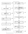
原位置薄片抜取りプロセスの概要
図1は、原位置薄片製造プロセスの諸ステップの概要を示す流れ図である。ステップ102で、半導体ウェーハなどの加工物200(図2)をデュアル・ビーム・システムの真空室(図示せず)に挿入する。ステップ104で、加工物の関心領域202を、例えば検査データ、試験データおよび/またはCADデータを使用して識別する。図2は、関心領域202を含む塊204を含む加工物200を示す。この体積204を、イオン・ビーム206によって薄片にする。薄片を抜き取る間および薄片を薄くする間の損傷から関心領域を保護するため、ステップ106で、保護層208を付着させる。ステップ108で、関心領域に隣接した位置に、処理用のイオン・ビーム206の位置合せまたはプローブの位置決めの基準点の役目を果たす1つまたは複数の基準マーク210をミリングする。
Overview of in-situ lamina extraction process FIG. 1 is a flow chart outlining the steps of the in-situ lamina manufacturing process. At
ステップ110で、関心領域の両側にトレンチをミリングし、図3に示されているように薄い薄片309を残す。薄片の調製中にスパッタリングされた材料が薄片に再付着しないように、いくつかの実施形態では、薄片の下に、FIBを使用して追加の切削部を形成する。図3は、関心領域202を含む薄片309を残すためにイオン・ビーム206によってトレンチ305がミリングされた加工物200の一部分を示す。しばしば、薄片の小さな領域または窓(図示せず)がさらに薄化される。この際、薄片の残りの部分は、機械的安定性を維持するのに十分な厚さのまま残される。この薄化操作は、基板から薄片を抜き取る前に、薄片が針上にある間に、または薄片がグリッドに取り付けられた後に実行することができる。
At
ステップ112で、イオン・ビームが、薄片の側部およびの底部の周囲をミリングし、取付けタブ308によって加工物に取り付けられた薄片を残す。取付けタブの位置および数は、このワークフローの必要性に応じて変更することができる。
At
薄片上の基準マークの製造
任意選択のステップ114で、薄片309に基準マーク306を形成する。図18は、基準マーク306がミリングされた薄片309を示す顕微鏡写真である。いくつかの実施形態では、基準マーク306が、X−Y平面における薄片309とTEMグリッドの位置合せ、および続くZ方向のグリッドの降着を容易にする。基準マークは、FIBを使用してミリングすることによって、またはFIBもしくはSEMを使用して材料を付着させることによって形成することができる。基準マークは単なる基準ターゲットであるため、付着を使用して基準マークを形成することも、または除去を使用して基準マークを形成することもできる。基準マーク306が関心領域の画像化に影響を及ぼさないように、この基準マークは、表面の関心領域から十分に離れた位置に、好ましくはTEMグリッドに溶接する部分に形成する。本明細書で使用するとき、用語「溶接」は、ビーム誘起付着によって材料を付加して取付け部を形成することを指し、冶金の場合のように、表面を溶かし充填材料を追加し、その材料が冷えて、金属を溶接する場合のような結合部を形成することを言うのではない。溶接部は、FIB付着によって、SEM付着によってまたは他のある方法によって形成することができる。この基準マークはさらに、薄化するプロセスの間に、特徴部分(feature)が薄くなるにつれてそれらの特徴部分がどのように変化しているのかを追跡するのを助けるのに役立つことがある。この基準マークは、原位置 STEMを実行しようとする場合、または独立型S/TEMで特定のゲートの位置を特定しようとするときにも役立ちうる。
Production of fiducial marks on the foil In an
この基準マークの形状は加工物に応じて変更される。電子回路試料のフィーチャは角張っている傾向があるため、電子回路に対しては円形の基準マークを選択するとよい。生命科学では、試料のフィーチャが丸みを帯びていたり曲線状だったりする傾向があるため、正方形の基準マークが必要となることがある。この基準マークの形状はケース・バイ・ケースで変更することができる。この基準マークは、薄片の表面にミリングされた形状を含み、または薄片を貫通して延びる特定の形状の穴を含むことができる。 The shape of this fiducial mark is changed according to the workpiece. A circular fiducial mark may be selected for the electronic circuit, as the features of the electronic circuit sample tend to be angular. In life sciences, square fiducial marks may be required as sample features tend to be rounded or curvilinear. The shape of the reference mark can be changed on a case-by-case basis. The fiducial marks may include features milled on the surface of the lamina or may include holes of a specific shape extending through the lamina.
グリッド降着中には、FIB画像の上半分またはSEM画像の下半分の何もない空間に他のフィーチャがないため、いくつかの用途では、この基準マークが、TEMグリッドへの薄片の取付けの成功率を向上させる。薄片を裏返した後に薄片の位置を精確に特定することをより容易にすることにより、この基準マークを使用して、マニピュレータの回転位置合せを微調整することもできる。 During grid accretion, there are no other features in the empty space in the upper half of the FIB image or the lower half of the SEM image, so in some applications this fiducial mark is a successful attachment of the flake to the TEM grid. Improve the rate. This fiducial mark can also be used to fine-tune the rotational alignment of the manipulator by making it easier to accurately identify the location of the slice after turning it over.
ステップ115で、プローブ先端310を有する試料プローブ301を薄片309に接触させ、または薄片309の近くに置く。後述するように、マシンビジョンを使用して、プローブ先端を見つけ、プローブ先端を薄片に対して移動させることによって、ステップ115を自動化することができる。
In
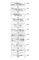
薄片へのプローブの取付け
図4は、図5および16に示されている、プローブ先端を薄片に自動的に取り付ける方法を示す流れ図である。いくつかの実施形態では、最初に、プローブ先端および薄片上の取付け点のx−y平面内における位置を特定し、次いで、プローブ先端を、x−y平面内において、取付け点のx−y座標まで移動させる。次いで、後述するように、表面に対して直角でないビームによって得た画像でプローブ先端および取付け点の位置を特定して、プローブ先端および取付け点のZ座標を決定することができるようにし、プローブ先端をz方向に取付け点まで移動させる。他の実施形態では、異なる経路に沿ってプローブが取付け点まで移動してもよく、異なる変位ベクトルを計算することができる。「物体の位置を決定する」および同様の言い回しは、物体の縁の位置または物体上の点の位置を決定することを含むことが理解される。この物体の縁の位置または物体上の点の位置の決定はしばしば、1つの物体の縁もしくは点を移動させて、別の物体の縁もしくは点の近くに置くこと、または別の物体の縁もしくは点に接触させることを目的とする。
Attaching the Probe to the Slice FIG. 4 is a flow chart showing the method of attaching the probe tip to the slice automatically, as shown in FIGS. In some embodiments, first locate the probe tip and the attachment point on the slice in the xy plane, and then locate the probe tip in the xy plane, the xy coordinate of the attachment point Move to The position of the probe tip and attachment point can then be identified in the image obtained by the beam not perpendicular to the surface, as described below, so that the Z coordinates of the probe tip and attachment point can be determined, In the z direction to the mounting point. In other embodiments, the probe may move to the attachment point along different paths, and different displacement vectors can be calculated. It is understood that "determining the position of an object" and similar phrases include determining the position of an edge of an object or the position of a point on an object. The determination of the position of the edge of the object or the position of a point on the object often involves moving the edge or point of one object to place it near the edge or point of another object, or the edge or point of another object Intended to be in contact with points.
ステップ402で、薄片309のそばの加工物上の基準マーク210の位置を、電子カラム1604からの電子ビームによって生成された上面画像を使用して特定する。ステップ404で、プローブ先端310を薄片309に溶接する位置503を、基準マーク210からのオフセット1602として決定する。これは、薄片309が、基準マーク210から既知の方向かつ既知の距離のところに位置するためである。ステップ406で、電子ビーム・カラム1604からの上面画像内で、プローブの先端310のx−y平面内における位置を特定する。ステップ408で、x−y平面内における先端310の位置とx−y平面内における薄片上の溶接位置503の位置との間のベクトルVxy(図16)を計算する。溶接位置503の位置は、基準マーク210からのオフセット1602によって決定される。ステップ410で、プローブ301を、ステージに対して平行な平面内において、計算されたベクトル距離Vxyだけ移動させて、プローブが、プローブを取り付ける薄片の面の上方に位置するようにする。
At
ステップ412で、図16に示された傾けられたイオン・カラム1606の視点からの画像を使用して、針の先端310の位置を特定する。ステップ413で、加工物上の基準マーク210の位置を特定する。ステップ414で、薄片上の溶接位置とプローブ先端310との間のベクトルVzを計算する。溶接位置は、基準マーク210からの既知のオフセットによって決定される。ステップ416で、ステージの平面に対して垂直なこのベクトルに沿った移動を使用して、プローブを、計算されたベクトル距離Vzだけ移動させる。Vzを決定する際には、三角法スカラーを使用して、イオン・カラム1606の斜めからの視点に対応する。すなわち、イオン・ビーム画像によるz距離を、イオン・ビームと表面法線の間の角度の正弦で除して、Vzの大きさを決定する。図16は、薄片の表面に取り付けられたプローブを示しているが、薄片の上面にプローブを溶接することもできる。薄片の上面の代わりに薄片の表面にプローブ先端310を溶接することによって、プローブのZ方向の位置決めの重要性が低下する。薄片の上面へのZ位置決めに誤差があると、薄片が損傷する可能性がある。プローブ先端と薄片の側面との間にわずかな隙間がある場合、その隙間は溶接操作中に埋められる。
At
プローブを薄片に取り付ける図1のステップ116は、ステップ418に示されているように、この画像上の薄片309に接触したプローブ先端310の位置に溶接ボックスを置くことによって実施することができる。プログラムは次いで、ビーム誘起付着による溶接に適したビーム・パラメータを使用して溶接位置でラスタリング(rastering)するようイオン・ビーム・カラムに指示する。ステップ420で、プローブ先端310を薄片309に溶接する。図5は、ガス噴射ノズル510によって導入されたW(CO)6などの前駆体ガスを分解して材料503を付着させることによって、薄片309に取り付けられているプローブ先端310を示す。いくつかの実施形態では、プローブ先端310を薄片の上面に取り付ける。他の実施形態では、プローブ先端310を、薄片の側面の関心領域202から十分に離れた位置に取り付ける。自動化されたプロセスに関しては、薄片を上面を通して取り付けるよりも、側面に取り付けた方が容易であることがある。プローブを、Z方向に、薄片に近い位置または薄片に接触する位置まで下ろすことができる。プローブは、固定された単一のZ値を有する上面ではなく、Z方向に延びる側面にあるため、取付け部のZ寸法が正確であるかどうかは重要ではない。
Attaching the Probe to the
この手順は次いで図1のステップ118へ進む。ステップ118では、タブ308を切断して、プローブ301に取り付けられた薄片を基板から分離する。ステップ120で、薄片をTEMグリッドへ移動させる。これについては後により詳細に説明する。ステップ122で、薄片をTEMグリッドに取り付ける。
The procedure then proceeds to step 118 of FIG. In
ステップ406および412では、ビームによって形成された画像中でプローブの位置を特定する必要がある。これは画像解析、つまりパターン認識または小塊検出(blob finding)によって実行することができる。プローブと薄片の間の近接または接触の判定は、電気回路を使用してプローブと薄片の間の接触を検出することによって、または静電容量センサを使用して近接を感知することによって支援することができる。このガイド方法が画像解析法である場合には、プローブ先端が認識可能な形状を有することを保証することによってプローブ先端の発見が容易になる。プローブ先端が認識可能な形状を有することを保証する1つの方法は、イオン・ビーム・ミリングによってプローブ先端を自動的に整形する方法である。
In
プローブ先端の整形
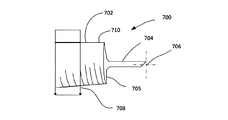
図6は、プローブ先端を自動的に整形する方法を示す流れ図である。図7および8に示されているように、プローブ700の太い部分を針702、細くされた部分を先端704、針が先端に変わる領域を肩705と呼ぶ。針は通常、約10度から約13度の間の角度で次第に細くなる。しかしながら、まっすぐな針を使用することもできる。ステップ602で、プローブを移動させて、プローブ先端が、イオン・ビームの視野の中心706の近くに位置するようにする。ステップ604で、図7に示されているように、針702の画像上にエッジ・ファインダ・ツール708を置き、それを使用して針の上縁710を見つける。ステップ606で、図8に示されているように、この画像上にエッジ・ファインダ・ツールを置き、それを使用して針の下縁を見つける。ステップ604および606は協力して針軸の「Y」位置を決定する。針軸の「Y」位置は、上縁と下縁の間の中央である。
Shaping the Probe Tip FIG. 6 is a flow diagram illustrating a method for automatically shaping the probe tip. As shown in FIGS. 7 and 8, the thick portion of the
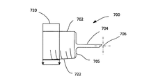
ステップ608で、針702の上縁を包含し下縁を包含しないより短いエッジ・ファインダ902(図9)を、針702の上縁に沿って移動させ、これを、エッジ・ファインダが針の上縁を見失うまで繰り返す。エッジ・ファインダが針の上縁を見失った点が、既存の針702の上縁の最大範囲および先端704の始まりを示す。所望の長さおよび幅を有する先端を形成するため、ステップ610で、ミリング・ボックス1002(図10)を置いて針をミリングする。既存の先端の端に対応する視野の中心からミリング・ボックスの反対端までの長さが、新しい先端の長さを決定する。針の軸からミリング・ボックス1002まで距離が、新しい先端の太さの1/2を決定する。いくつかの実施形態では、先端の太さが、10ミクロン未満であることが好ましく、5ミクロン未満であることがより好ましく、3ミクロン未満であることがよりいっそう好ましく、約2.5ミクロンであることが最も好ましい。ステップ612で、プローブの所望の先端長さの始まりからプローブ先端908の端までを画像の中心に置く。ステップ612でのミリングは、3nAから30nAの間、より好ましくは5nAから20nAの間、よりいっそう好ましくは約8nAから15nAの間の大きなビーム電流でのバルク・ミリングである。ステップ614で、同様のミリングを実行して、所望のプローブ先端よりも下方の材料を除去する。図11は、先端の長さを延ばすこのバルク・ミリングが完了した後の針を示す。
At
ステップ614および616のバルク・ミリングの後、ステップ618で、プローブ先端の全長に沿って断面クリーニング(cleaning cross section)を実行する。「断面クリーニング」は、最終的な切削面位置に向かってゆっくりと進むライン・ミリングであり、所望の最終切削面に対して平行なラインに沿ってビームが前後に掃引し、間隔を置いて、所望の最終切削面に向かってラインを前進させ、これを所望の最終切削面に達するまで続ける。この間隔は、ミリングの放射線量(dose)によって決定される。この放射線量は普通、ナノクーロン/平方マイクロメートルで示され、実質的に、単位面積当たりいくつのイオンが加工物に衝突するのかを規定する方法である。断面クリーニングを使用するときには通常、そのライン走査が増分される前に、切削面の上面からトレンチの底までの全ての材料が除去されることを保証する放射線量が設定される。
After bulk milling at
ステップ620で、プローブを90度回転させ、ステップ610から618を繰り返す。図6のプロセスの結果は、図12に示されているような直方柱(rectangular prism)状の形状に整形された既知の長さの先端を有するプローブである。針702は次第に細くなるため、針と先端の間の肩の高さは、使用中に針が時間の経過とともに短くなるにつれて増大する。他の先端形状および回転角を使用することもできる。
At
接触時のプローブと基板の間の角度のため、いくつかの実施形態では、図13に示されているように、プローブ先端704の端を斜めにミリングすることが好ましい。次いで、図14に示されているようにプローブ先端704を薄片309に接触させると、プローブの端1302が薄片309の側面と平行になる。プローブ先端を切削する好ましい角度は、試料室内でプローブが装着される角度によって異なる。さらに、鋭い角およびまっすぐな線は画像認識ソフトウェアによって容易に識別され、そのため、この形状は、プローブの画像認識の信頼性を高め、薄片へのプローブの取付けを改善する。したがって、好ましいプローブ先端の形状は「鑿(のみ:chisel)形」である。すなわち、遠位縁1302は長軸に対して垂直ではなく、長縁と90度では交差しない。
Because of the angle between the probe and the substrate upon contact, in some embodiments, as shown in FIG. 13, it is preferable to mill the end of the
この鑿形の先端は、イオン・ビームでミリングすることによって生み出すことができる。鑿形の形状を生み出すため、ステップ622で、図15に示されているように、プローブ先端の端にミリング・ボックス1502を置く。ステップ624で、プローブ先端をミリングして、斜めの先端を形成する。画像認識では先端の形状が認識可能であることが重要であるため、1つの薄片と別の薄片の間で先端の形状を維持することが望ましいことがある。試料プローブの縁および先端の位置に関する正確な情報なしに、プローブがたどらなければならない後述する移動経路を計算することは難しい。先端の形状が認識可能であることを保証するため、薄片を抜き取るごとに、または2つもしくは3つの薄片を抜き取るごとに先端を整形し直すことが好ましい。薄片が移送されるときには、薄片が切り離されるたびに、プローブ先端の一部がしばしば失われ、そのため、薄片の取付け部は、次第に細くなるプローブの上の方へ段々と移動し、それによって肩がより高くなる。この自動プローブ再整形手順は、プローブが短くなったときでもプローブ先端の外観を均一に保つのに役立つ。
This wedge shaped tip can be produced by milling with an ion beam. In order to create a wedge shape, at
この自動プローブ再整形の重要な態様は、それが、抜取りプロセスの一部として、粒子ビーム機器内で「原位置」で実行されることである。 An important aspect of this automatic probe reshaping is that it is performed “in situ” within the particle beam instrument as part of the sampling process.
ステップ626は、任意選択で、図3に示されているように、プローブ先端に、基準マーク302がミリングされることを示している。図19は、プローブ先端310にミリングされた基準マーク302の顕微鏡写真を示す。この基準マークを使用して、ステップ115で薄片に対するプローブ先端の位置を決定するプローブ先端の位置の自動画像認識を容易にすることができる。さらに、この基準マークを使用して、画像認識プログラムが先端を探すエリアをより精緻にすることができ、この基準マークは、使用するエッジ・ファインダの正確さを増大させる。この基準マークは、プローブ先端から既知の距離のところにミリングすることができる。画像認識によってこの基準マークを見つけると、プローブ先端の位置をより容易に特定することができる。
Step 626 optionally indicates that the
この基準マークは、画像中において先端位置を機械認識する第2の方法を可能にするため、この基準マークを、整形された先端と一緒にまたは整形された先端の代わりに使用することができる。 Since this reference mark allows a second way of machine recognition of the tip position in the image, this reference mark can be used with or instead of the shaped tip.
プローブに基準マークがミリングされる場合には、プローブ先端を薄片まで移動させるときに、基準マークの位置を使用してエッジ・ファインダを置き、それによってプローブ先端の端の位置を特定することができる。例えば、プローブ先端の縁がエッジ・ファインダの探索ボックス内にあることを保証する十分な大きさの固定された距離だけ、エッジ・ファインダを、基準マークの端から延ばすことができる。そのエッジ・ファインダは、プローブ先端の縁の位置を特定し、プローブ先端と薄片の間のベクトル変位を計算することによって、プローブを薄片に自動的に接触させることを容易にするであろう。その薄片がTEMグリッドに取り付けられときには、次の薄片を取り上げるときに使用するプローブ先端に、新しい基準マークをミリングすることができる。 If the fiducial mark is milled on the probe, the position of the fiducial mark can be used to locate the edge finder and thereby locate the end of the probe tip when moving the probe tip to the slice. . For example, the edge finder can extend from the end of the fiducial mark by a fixed distance large enough to ensure that the edge of the probe tip is within the search box of the edge finder. The edge finder will facilitate contacting the probe automatically with the foil by locating the edge of the probe tip and calculating the vector displacement between the probe tip and the foil. When the foil is attached to the TEM grid, a new fiducial mark can be milled into the probe tip used to pick up the next foil.
この基準マークは、針を薄片まで正確に移動させて、薄片を傷つけることなく溶接することができるように、画像認識ソフトウェアが先端の端を容易に識別することを可能にする。いくつかの実施形態では、プローブ先端に円形の基準マークがミリングされるが、異なる形状の基準マークを使用することもできる。この新しい基準マークは、加工物から次の薄片を取り上げるために使用される。 This fiducial mark allows the image recognition software to easily identify the end of the tip so that the needle can be accurately moved to the foil and welded without damaging the foil. In some embodiments, a circular fiducial mark is milled at the probe tip, although different shaped fiducial marks can be used. This new fiducial mark is used to pick up the next slice from the workpiece.
この項で説明したとおり、プローブ先端を整形しおよび/またはプローブに基準マークを追加するプロセスは、薄片の抜取りの自動化において特に有用である。しかしながら、薄片を抜き取るたびにこのプロセスを実行することが常に必要であるというわけではない。いくつかのケースでは、このプローブ先端の整形および/または基準マークの追加が定期的に実行されるが、薄片を抜き取るごと必ず実行されるというわけではない。例えば、プローブ先端の整形は、薄片を1つ抜き取るごとに、または薄片を2つ抜き取るごとに、または薄片を3つ抜き取るごとに、または薄片を4つ抜き取るごとに、または薄片を5つもしくはそれ以上抜き取るごとに実行することができる。
プローブ先端を薄片まで移動させる際の画像減算の使用
画像中の特定のフィーチャの画像認識を容易にするためにいくつかの実施形態で使用される他の技法が画像減算である。当面の作業に無関係の複数の外部フィーチャを画像が有するときには、それらのフィーチャが、物体の位置を自動的に特定しようとする試みを複雑にすることがある。ターゲット物体を移動させた複数の画像を撮影することによって、それらの外部フィーチャを排除することができる。それらの複数の画像の減算を実行し、それにより静止した外部フィーチャを排除することができる。関心の物体の位置を背景の干渉なしに決定するためには、エッジ・ファインダまたは他の自動計測ツール(automated metrology tool)を配置する。
As described in this section, the process of shaping the probe tip and / or adding fiducial marks to the probe is particularly useful in the automation of flake extraction. However, it is not always necessary to carry out this process each time a slice is removed. In some cases, this probe tip shaping and / or addition of fiducial marks is performed periodically, but not necessarily every time a slice is extracted. For example, the probe tip can be shaped every time one slice is drawn, every two slices, every three slices, every fourth slice, or five or more slices. It can be executed each time it is removed.
Use of Image Subtraction in Moving the Probe Tip to a Slice Another technique used in some embodiments to facilitate image recognition of particular features in the image is image subtraction. When an image has multiple external features that are not relevant to the task at hand, these features can complicate attempts to automatically locate the object. By capturing multiple images with the target object moved, those external features can be eliminated. The subtraction of those multiple images can be performed, thereby eliminating stationary external features. In order to determine the position of the object of interest without background interference, an edge finder or other automated metrology tool is placed.
図17a〜17fは、プローブ先端を識別して、プローブ先端の位置を正確に決定することができるようにするのに使用する画像を示す。プローブ先端の位置を正確に決定した後、プローブを薄片に取り付ける薄片溶接位置までプローブ先端を移動させるためのベクトルを計算することができる。図17a〜17cは、加工物表面に対して垂直に向けられた電子ビームによる画像を示す。これらの画像を使用して、X−Y平面内におけるプローブ先端の位置を決定する。図17d〜17fは、加工物表面に対して45度、52度などの角度に向けられたイオン・ビームによる画像を示す。これらの画像を使用して、プローブ先端と薄片上に取付け点との間のZ座標の差を決定する。 Figures 17a-17f show images used to identify the probe tip so that the position of the probe tip can be accurately determined. Once the position of the probe tip has been accurately determined, a vector can be calculated to move the probe tip to the foil weld location where the probe is attached to the foil. Figures 17a-17c show images with an electron beam directed perpendicular to the workpiece surface. These images are used to determine the position of the probe tip in the X-Y plane. Figures 17d-17f show images from ion beams directed at angles such as 45 degrees, 52 degrees, etc. with respect to the workpiece surface. These images are used to determine the Z coordinate difference between the probe tip and the attachment point on the slice.
図20aおよび20bは、自動化されたリフトアウトを容易にするための画像減算技法の使用を示す流れ図である。図20aのステップ2002で、図17aに示されているようなプローブ先端310の上面画像を形成する。ステップ2004で、ステップ2002で撮影した画像の視野の中にプローブが依然としてあるようにして、プローブを、x−y平面内で少しだけ移動させる。ステップ2006で、図20bに示されているような第2の画像を、好ましくは図20aの画像を形成するのに使用したビーム設定と同じビーム設定を使用して得る。ステップ2008で、図17bの画像から図17aの画像を差し引く。画像を差し引くとは、一方の画像の画素のグレー・レベルから他方の画像の画素のグレー・レベルを差し引くことを意味する。それらの画像の撮影と撮影の間にビーム・パラメータが変化しない場合には、それらの画像は位置合せされているはずであるが、いくつかの実施形態では、減算の前にそれらの画像の位置合せを実施する。いくつかの実施形態では、この減算プロセスの前および/または後に、メジアン・フィルタ(median filter)、ガウス平滑フィルタ(Gaussion smoothing filter)、しきい値処理(threshholding)、膨張(dilation)/収縮(erosion)操作などの画像処理機能を、任意の画像に対して適用する。図17cは、減算後の画像1702を示し、図17aからの寄与が破線で示されている。背景は実質的に排除されており、移動させたプローブ先端は、エッジ・ファインダまたは他の計測ツールによって位置を精確に特定することがより容易になっている。ステップ2010で、図17cの減算後の画像にエッジ・ファインダを適用して、減算後の画像中のプローブ先端の位置を特定する。図20に記載された手順は、上面画像中のプローブ先端の位置を特定するステップ406のステップを実行する1つの方法である。他の方法を使用することもできる。プローブ先端に基準マークをミリングする実施形態では、この画像減算技法を使用して、基準マークの位置をより精確に特定することができる。いくつかの実施形態では、この画像減算法の使用が、プローブ先端の基準マークの必要性を排除した。他の実施形態では、プローブ先端の基準マークが、画像減算技法の必要性を排除した。
Figures 20a and 20b are flow diagrams illustrating the use of image subtraction techniques to facilitate automated lift-out. At
図20bのステップ2020から2028は、図4のステップ412に示されているようにプローブ先端のZ方向の位置を精確に決定する1つの方法を説明する。ステップ2020で、図17dに示されているような第1の画像を、表面に対して垂直に向けられていないビーム、この場合にはイオン・ビームを使用して得る。ステップ2022で、ビーム走査エリアを変更しなくてもプローブ先端が依然として見えるようにして、プローブを、Z方向に少しだけ移動させる。ステップ2024で、第2の画像(図17e)を、図17dの画像を得るのに使用したビーム設定と同じビーム設定を使用して得る。ステップ2026で、図17eの画像から図17dの画像を差し引いて、プローブ先端の位置の変化を図17eに示し、加工物表面の画像を排除してプローブ先端の認識を容易にする。ステップ2028で、エッジ・ファインダを使用して、図17fの画像中のプローブ先端の位置を特定する。プローブ先端のZ方向の位置を特定した後、ステップ414で、その位置を使用して、ベクトルVzを決定することができる。
プローブを識別する場合には、画像に対してプローブを少しだけ移動させて2つの画像を得ることによって、それらの画像の減算を実行し、先端の外側包絡線(outer envelope)に関連した境界を決定することができる。このようなプロセスは、プローブの包絡線の位置の決定を大いに支援する。複数の移動を実行して追加の情報を得ることができる。さらに、既知の量だけ移動させ、その既知の量の移動を解析の一部として利用することが有利となることがある。 When identifying a probe, the probe is moved slightly relative to the image to obtain two images, which are then subtracted between the images to determine the boundary associated with the outer envelope of the tip. Can be determined. Such a process greatly aids in the determination of the position of the envelope of the probe. Multiple moves can be performed to obtain additional information. Furthermore, it may be advantageous to move by a known amount and to use the known amount of movement as part of the analysis.
TEMグリッドへの薄片の取付け
図21は、プローブ301に取り付けられた薄片309をTEMグリッドに取り付けるプロセスを説明する流れ図である。理解されるとおり、TEMグリッドは、TEMで観察するために薄片が装着される構造体であり、本出願の出願人によって市販されている。グリッド上に薄片を正確に降着させるためには、薄片が取り付けられたプローブおよびグリッドの正確な位置が、3つの全ての次元において既知であるべきである。3次元位置特定には、第1のビームに対して傾けられた第2のビームの視点を使用することができる。図22の画像減算ルーチンを使用して、薄片が取り付けられたプローブおよび試料グリッドの位置を、この第2の視点を使用することによって識別することができる。
Attaching a Slice to a TEM Grid FIG. 21 is a flow chart illustrating the process of attaching a
ステップ2102で、薄片309の位置を特定する。いくつかの実施形態では、パターン認識ソフトウェアを使用して薄片の位置を自動的に特定する。このパターン認識は、薄片の位置特定を容易にする図18に示された薄片上の基準マーク306によって容易にすることができる。薄片の位置特定は、減算画像化を使用して容易にすることもできる。
At
図22aおよび22bは、減算画像化を使用して薄片の位置を特定する諸ステップを示す。図22aのステップ2202で、図23aに示されているように、プローブ先端301の端にある薄片309を示す上面SEM画像を取得する。この画像ではTEMグリッド2302が見えている。ステップ2204で、薄片301が視野の中に留まるようにして、薄片を保持しているプローブを、x−y平面内で短い距離だけ移動させる。ステップ2206で、図23aを取得するのに使用したシステム設定を使用して、図23bに示された別の画像を取得する。ステップ2208で、図23bの画像から図23aの画像を差し引き、その結果として図23cの画像を得る。図23cは、薄片309およびプローブ先端301を示しているが、その一方で、背景およびTEMグリッド2302の多くを排除している。ステップ2210で、この減算後の画像にエッジ・ファインダまたは他の計測ツールを適用して、薄片の位置を精確に決定する。
Figures 22a and 22b show the steps of locating a slice using subtraction imaging. At
薄片のx−y平面内の位置を決定した後、ステップ2104(図21)で、TEMグリッド上の取付け点の位置を決定する。ステップ2220(図22)で、図23dに示されているように、TEMグリッド2302の上面SEM画像を取得する。ステップ2222で、TEMグリッドが図23dの視野の中に留まるようにして、TEMグリッドを支持しているステージをわずかに移動させる。ステップ2224で、第1の画像と同じビーム設定を使用して第2の画像を取得する。ステップ2226で、図23eに示された第2の画像から図23dに示された第1の画像を差し引き、その結果として図23fの画像を得る。ステップ2228で、この減算後の画像にエッジ・ファインダまたは他の計測ツールを適用して、TEMグリッド2302の位置を精確に決定する。
After determining the position of the slice in the xy plane, in step 2104 (FIG. 21), the position of the attachment point on the TEM grid is determined. In step 2220 (FIG. 22), an upper surface SEM image of the
ステップ2106で、図24に示されているように、薄片309とTEMグリッド2412上の取付け点との間のベクトルVxy変位を決定する。ステップ2108で、X−Y平面内において、薄片を、取付け点位置のすぐ上の位置まで移動させる。
At
ステップ2110で、薄片のZ寸法を決定することができるような異なる視点を提供するもう一方のビームを使用して、薄片の位置を特定する。薄片の位置は例えば、薄片上の基準マーク306によって支援された画像認識を使用することによって、または画像減算技法を使用することによって、またはこれらの両方の技法を使用することによって特定することができる。
At
図25aおよび25bは、画像減算を使用してZ変位を決定する諸ステップを示す流れ図である。ステップ2502で、図26aに示されているように、薄片を示す斜めのFIB画像を取得する。ステップ2504で、薄片が、このイオン・ビーム画像の視野の中に留まるようにして、薄片を保持しているプローブをZ方向に短い距離だけ移動させる。ステップ2506で、図26bに示されているような別の画像を取得する。図26bの画像は、図26aを取得するのに使用したシステム設定を使用して取得する。ステップ2508で、図26bの画像から図26aの画像を差し引き、その結果として図26cの画像を得る。この画像は、薄片およびプローブを示しているが、その一方で背景の多くを排除している。ステップ2510で、この減算後の画像にエッジ・ファインダまたは他の計測ツールを適用して、薄片の位置を精確に決定する。
25a and 25b are flow diagrams showing the steps of determining Z displacement using image subtraction. At
FIBの視点から薄片の位置を決定した後、ステップ2112で、TEMの取付け点の位置を、FIBの視点から決定する。ステップ2520で、図26dに示されているように、TEMグリッド2302の角度のついた画像を取得する。ステップ2522で、TEMグリッド2302が図26dの視野の中に留まるようにして、TEMグリッド2302を支持しているステージをZ方向に少しだけ移動させる。ステップ2526で、図26eから図26dの画像を差し引き、その結果として図26fの画像を得る。ステップ2528で、この減算後の画像にエッジ・ファインダまたは他の計測ツールを適用して、TEMグリッドの位置を精確に決定する。
After determining the position of the foil from the FIB's point of view, in
ステップ2114で、薄片とTEMグリッド上の取付け点との間の高さの差であるベクトルVzを、FIB画像内の薄片とTEMグリッドの取付け点の間の距離を使用し、この距離を、FIB軸と表面に対する法線の間の角度の正弦で除することによって決定する。ステップ2116で、プローブを、計算された距離VzだけZ方向に移動させる。
In
ステップ2118で、図27に示されているように、薄片309をTEMグリッド1302に溶接する。イオン・ビーム206を使用して、ガス噴射針410からの前駆体ガスを分解し、それによって溶接材料2702を付着させて、薄片309を取り付ける。ステップ2120で、図28に示されているように、イオン・ビームを使用して、プローブ301を薄片309から切り離す。あるいは、プローブと薄片を別々に移動させることによって、それらを切り離すこともできる。薄片とプローブの間の接続を切るためにミリング・ボックス2802が配置される。任意選択のステップ2124で、例えば図19に示されているように、プローブ先端に基準マーク302をミリングして、次の薄片のリフトアウト中に画像認識ソフトウェアがプローブ先端をより容易に認識することができるようにする。任意選択のステップ2126で、図29に示されているように、TEMグリッド上に薄片が装着されている間に薄片をさらに薄くする。
At
第1の薄片を形成し、その薄片をTEMグリッドまで移動させた後、後続の薄片に対してこのプロセスを繰返すことができる。それに加えてまたはその代わりに、リフトアウトする次の薄片にプローブ先端が接近する前に、図6に記載されているようにしてプローブ先端を再整形して、プローブ先端が、自動画像認識ソフトウェアによって容易に認識されるようにする。 After the first slice has been formed and transferred to the TEM grid, this process can be repeated for subsequent slices. Additionally or alternatively, before the probe tip approaches the next slice to be lifted out, the probe tip is reshaped as described in FIG. Make it easy to recognize.
以上では、画像減算ルーチンに対して2つの画像を使用することを説明したが、3つ以上の画像を使用することもできる。減算画像化は、画像解析中に偽陽性を示すであろうエリアにおいても特定の物体の識別を可能にする。 Although the use of two images has been described above for the image subtraction routine, more than two images can be used. Subtraction imaging allows identification of specific objects even in areas that will show false positives during image analysis.
本発明の方法を実行する典型的なシステム
図30は、本発明のさまざまな実施形態の諸ステップを実行する目的に使用することができる典型的なデュアル荷電粒子ビーム・システムを示す。このシステムは、電子源3000とビーム整形レンズ3001、3003とを備える電子ビーム・カラム3002を有し、電子ビーム3016を導く。このシステムはさらに、イオン源3020とイオン集束レンズ3019、3018とを備えるイオン・ビーム・カラム3021を有し、イオン・ビーム3017を導く。これらのビームは、関心領域307を含む試料3013に向かって導かれる。試料3013は、x−y−z方向に移動し、回転し、傾くことができる5軸1次ステージ3012上に配置される。この1次ステージ上には、TEMグリッド3022を保持するTEMグリッド・ホルダ3024が装着されている。薄片の取付けおよび処理のためにTEMグリッドを操作する更なる自由度を確認するために、任意選択で、TEMグリッド・ホルダ3024を2次ステージ3026上に装着することもできる。このシステムはさらに、粒子検出器3015、ガス導入システム3014および試料操作プローブ3011を含む。試料操作プローブ3011は、プローブ先端をx−y−z方向に移動させることができ、プローブ軸を軸にして回転することができる。荷電粒子ビーム・カラム、検出器、ガス導入システムおよび試料操作プローブは真空室3004内に収容されており、真空室3004は、真空ポンプ3009によって排気される。荷電粒子カラム、検出器、ガス導入システムおよび試料プローブは制御装置3008によって制御され、制御装置3008は、記憶装置3028に記憶されたコンピュータ命令を取り出すことができる。
Exemplary System for Performing the Method of the Present Invention FIG. 30 illustrates an exemplary dual charged particle beam system that can be used to perform the steps of various embodiments of the present invention. The system comprises an
本発明の以上の説明は主に、TEM薄片を生成する方法を対象としており、この方法は、堅牢さ、繰返し性および速度の面で有利であり、したがって自動化に適しているが、この方法の操作を実行する装置も本発明の範囲に含まれるであろうことを認識すべきである。さらに、本発明の実施形態は、コンピュータ・ハードウェアもしくはソフトウェアまたはハードウェアとソフトウェアの組合せによって実現することができることを認識すべきである。本発明の方法は、標準プログラミング技法を使用した、本明細書に記載された方法および図に基づくコンピュータ・プログラムとして実現することができる。ここで言うコンピュータ・プログラムには、コンピュータ・プログラムを含むように構成されたコンピュータ可読の記憶媒体が含まれ、そのように構成された記憶媒体は、コンピュータを、事前に決定された特定の方式で動作させる。コンピュータ・システムと通信するため、それぞれのプログラムは、高水準手続き型プログラミング言語またはオブジェクト指向プログラミング言語で実現することができる。しかしながら、所望ならば、それらのプログラムを、アセンブラ言語または機械語で実現することもできる。いずれにせよ、その言語は、コンパイルまたは解釈される言語とすることができる。さらに、そのプログラムは、そのプログラムを実行するようにプログラムされた専用集積回路上で実行することができる。 The above description of the present invention is mainly directed to a method of producing TEM slices, which is advantageous in terms of robustness, repeatability and speed, and thus suitable for automation, It should be recognized that apparatus for performing the operations would also fall within the scope of the present invention. Furthermore, it should be appreciated that embodiments of the present invention can be realized by computer hardware or software or a combination of hardware and software. The method of the present invention can be implemented as a computer program based on the methods and figures described herein using standard programming techniques. The computer program referred to herein includes a computer-readable storage medium configured to include a computer program, and the storage medium configured in such a manner causes the computer to be in a predetermined manner. Make it work. Each program may be implemented in a high level procedural or object oriented programming language to communicate with a computer system. However, if desired, the programs can also be implemented in assembler or machine language. In any case, the language can be the language to be compiled or interpreted. Furthermore, the program can be run on a dedicated integrated circuit programmed to run the program.
さらに、方法論は、限定はされないが、荷電粒子ツールもしくは他の画像化装置とは別個の、または荷電粒子ツールもしくは他の画像化装置と一体の、または荷電粒子ツールもしくは他の画像化装置と通信するパーソナル・コンピュータ、ミニコンピュータ、メインフレーム、ワークステーション、ネットワーク化されたコンピューティング環境または分散コンピューティング環境、コンピュータ・プラットホームなどを含む、任意のタイプのコンピューティング・プラットホームで実現することができる。本発明の諸態様は、取外し可能であるか、またはコンピューティング・プラットホームと一体であるかを問わない、ハードディスク、光学式記憶媒体、RAM、ROMなどの記憶媒体上または記憶装置上に記憶された機械可読コードであって、プログラム可能なコンピュータが、本明細書に記載された手順を実行するために、その記憶媒体または記憶装置を読んだときに、そのコンピュータを構成し、動作させるために、そのコンピュータが読むことができるように記憶された機械可読コードとして実現することができる。さらに、機械可読コードまたは機械可読コードの一部を、1つまたは複数の有線または無線ネットワークを介して伝送することができる。本明細書に記載された発明は、マイクロプロセッサまたは他のデータ処理装置と連携して上述の諸ステップを実現する命令またはプログラムを含む、これらのさまざまなタイプのコンピュータ可読記憶媒体、およびその他のさまざまなタイプのコンピュータ可読記憶媒体を含む。本発明はさらに、本明細書に記載された方法および技法に従ってプログラムされたコンピュータを含む。 Further, the methodology is not limited, but is separate from the charged particle tool or other imaging device, or integral with the charged particle tool or other imaging device, or in communication with the charged particle tool or other imaging device Can be implemented on any type of computing platform, including personal computers, minicomputers, mainframes, workstations, networked or distributed computing environments, computer platforms, and the like. Aspects of the invention are stored on a storage medium or storage device, such as a hard disk, optical storage medium, RAM, ROM, whether removable or integral with a computing platform. Machine readable code, which is a programmable computer, configured to operate and operate when the computer reads the storage medium or storage device to perform the procedures described herein. It can be implemented as machine readable code stored so that the computer can read it. Further, the machine readable code or a portion of the machine readable code may be transmitted over one or more wired or wireless networks. The invention described herein includes these various types of computer-readable storage media, including instructions or programs that implement the steps described above in conjunction with a microprocessor or other data processing apparatus, and various others. Various types of computer readable storage media. The invention further includes a computer programmed according to the methods and techniques described herein.
以上の説明の多くは半導体ウェーハを対象としているが、本発明は、適当な任意の基板または表面に対して使用することができる。 Although much of the above description is directed to semiconductor wafers, the present invention can be used on any suitable substrate or surface.
本発明のいくつかの実施形態は、荷電粒子ビーム・システム内での自動化された試料調製の方法であって、
1つまたは複数の荷電粒子ビーム・システムおよび試料操作プローブを特徴とする真空室内に加工物を装填することと、
加工物上の関心領域を画像化することと、
薄い切片の周囲の材料を、集束イオン・ビームを使用して除去することと、
薄い切片を支持している材料を除去し、小さな取付け構造体によって大きな加工物に取り付けられた薄い切片を残すことと、
イオン・ビームを使用して材料を除去することによって、試料操作プローブの先端を整形することと、
薄い切片に対する先端の位置を決定するために、先端の既知の形状を使用することと、
薄い切片に対する先端の位置を使用して、薄い切片のすぐ近くに試料プローブを自動的に移動させることと、
試料プローブを薄い切片に取り付けることと、
大きな加工物に薄い切片を接続している支持構造体を、イオン・ビームを使用して除去することであって、薄い切片が試料プローブだけによって支持されているようにすることと、
試料プローブを、取り付けられた薄い切片とともに、薄い切片用の試料グリッドが位置する領域まで移動させることと、
試料グリッドおよびプローブならびに取り付けられた薄い切片が位置する領域を画像化することと、
薄い切片が試料グリッドのすぐ近くにくるように、プローブを自動的に移動させることと、
薄い切片を試料グリッドに取り付けることと、
薄い切片から試料プローブの先端を取り外すことと
を含む方法を提供する。
Some embodiments of the present invention are methods of automated sample preparation within a charged particle beam system comprising:
Loading the workpiece into a vacuum chamber featuring one or more charged particle beam systems and a sample manipulation probe;
Imaging the region of interest on the workpiece;
Removing the material around the thin section using a focused ion beam;
Removing the material supporting the thin section, leaving the thin section attached to the large workpiece by the small mounting structure;
Shaping the tip of the sample manipulation probe by removing material using an ion beam;
Using the known shape of the tip to determine the position of the tip relative to the thin section;
Automatically moving the sample probe in close proximity to the thin section using the tip position relative to the thin section;
Attaching the sample probe to a thin section;
Removing the support structure connecting the thin section to the large workpiece using an ion beam, such that the thin section is supported only by the sample probe;
Moving the sample probe with the attached thin section to the area where the sample grid for the thin section is located;
Imaging the region where the sample grid and probe and the attached thin section are located;
Automatically moving the probe so that the thin section is in close proximity to the sample grid;
Attaching a thin section to the sample grid;
Removing the tip of the sample probe from the thin section.
いくつかの実施形態では、薄い切片が断面観察用の切片である。 In some embodiments, the thin section is a section for cross-sectional observation.
いくつかの実施形態は、試料プローブの移動を誘導するために、画像解析を使用する。 Some embodiments use image analysis to guide the movement of the sample probe.
いくつかの実施形態では、試料操作プローブの先端を整形することが、先端を、機械認識が可能な形状に整形することを含み、薄い切片に対する先端の位置を決定するために、先端の既知の形状を使用することが、プローブ先端の位置を決定するために機械認識が可能な先端の形状を認識するために画像認識ソフトウェアを使用することを含む。 In some embodiments, shaping the tip of the sample manipulation probe includes shaping the tip into a shape that is machine recognizable to determine the tip position relative to the thin section. Using the shape involves using image recognition software to recognize the shape of the tip that is capable of machine recognition to determine the position of the probe tip.
いくつかの実施形態では、先端が鑿形に整形される。 In some embodiments, the tip is shaped like a bowl.
いくつかの実施形態は、プローブを薄い切片または試料グリッドまで移動させるための軌道を決定するために、プローブの位置を画像解析を使用して特定することを含む。 Some embodiments include identifying the position of the probe using image analysis to determine the trajectory for moving the probe to a thin section or sample grid.
いくつかの実施形態では、画像解析が画像減算を使用する。 In some embodiments, image analysis uses image subtraction.
いくつかの実施形態は、プローブと前記薄い切片の間のXYベクトルを、1つの荷電粒子ビームによる画像に基づいて計算し、プローブと薄い切片の間のZベクトルを、第2の粒子ビームによる画像に基づいて計算することをさらに含む。 Some embodiments calculate the XY vector between the probe and the thin section based on the image with one charged particle beam, and the Z vector between the probe and the thin section with the second particle beam Further comprising calculating based on.
いくつかの実施形態では、この方法が、プローブから薄い切片が取り外された後に先端を再整形することをさらに含む。 In some embodiments, the method further comprises reshaping the tip after removing the thin section from the probe.
いくつかの実施形態では、この方法が、薄い切片の側面の関心領域から離れた位置にプローブを取り付けることをさらに含む。 In some embodiments, the method further comprises attaching the probe at a position away from the region of interest on the side of the thin section.
いくつかの実施形態では、この方法が、薄い切片が試料グリッドに取り付けられた後に薄い切片をさらに薄くすることをさらに含む。 In some embodiments, the method further comprises thinning the thin section after the thin section is attached to the sample grid.
本発明のいくつかの実施形態は、荷電粒子システム内での自動化された試料調製のための装置であって、
加工物を収容する真空室と、
真空室内の加工物を画像化し、加工物に対して作用する荷電粒子ビームを生成する少なくとも2つの荷電粒子ビーム・カラムと、
真空室内の加工物を保持し、加工物を移動させる可動試料ステージと、
荷電粒子ビームが衝突したときに試料から放出された荷電粒子から画像を形成する荷電粒子検出器と、
サブミクロンの位置決めが可能な試料操作プローブと、
荷電粒子ビーム誘起付着用の前駆体ガスを供給するガス噴射システムと、
この装置の動作を制御する制御装置と、
制御装置によって実行される、上記請求項[000157]1の方法を実行するためのコンピュータ命令を記憶するコンピュータ可読の記憶装置と
を備える装置を提供する。
Some embodiments of the present invention are devices for automated sample preparation within a charged particle system comprising:
A vacuum chamber for containing the workpiece,
At least two charged particle beam columns for imaging a workpiece in a vacuum chamber and producing a charged particle beam acting on the workpiece;
A movable sample stage that holds the workpiece in the vacuum chamber and moves the workpiece;
A charged particle detector that forms an image from charged particles emitted from the sample when the charged particle beam collides;
A sample handling probe capable of submicron positioning;
A gas injection system for supplying a precursor gas for charged particle beam induced deposition;
A control device that controls the operation of the device;
A computer readable storage device storing computer instructions for performing the method of
いくつかの実施形態では、この装置が、2つの荷電粒子ビーム・システムを含む装置をさらに備える。 In some embodiments, the apparatus further comprises an apparatus that includes two charged particle beam systems.
いくつかの実施形態では、加工物を画像化し、加工物に対して作用する荷電粒子ビームを生成する少なくとも2つの荷電粒子ビーム・カラムが、電子ビーム・カラムおよびイオン・ビーム・カラムを含む。 In some embodiments, at least two charged particle beam columns that image a workpiece and generate charged particle beams that act on the workpiece include an electron beam column and an ion beam column.
いくつかの実施形態では、コンピュータ記憶装置が、荷電粒子ビームによって形成された画像を解析するためのコンピュータ命令を含み、この画像解析が、薄い切片が取り付けられた試料操作プローブの位置または薄い切片が取り付けられていない試料操作プローブの位置を特定するようにプログラムされている。 In some embodiments, the computer storage device comprises computer instructions for analyzing an image formed by the charged particle beam, wherein the image analysis comprises the position of the thin section mounted sample manipulation probe or the thin section It is programmed to locate the unmounted sample manipulation probe.
いくつかの実施形態では、この画像解析が画像減算を使用して実行される。 In some embodiments, this image analysis is performed using image subtraction.
いくつかの実施形態では、材料除去手段が集束イオン・ビームである。 In some embodiments, the material removal means is a focused ion beam.
いくつかの実施形態では、集束イオン・ビームが薄い切片上に基準マークを形成するようにするコンピュータ命令をコンピュータ記憶装置が含む。 In some embodiments, the computer storage device comprises computer instructions for causing the focused ion beam to form a fiducial mark on the thin section.
いくつかの実施形態では、集束イオン・ビームがプローブ上に基準マークを形成するようにするコンピュータ命令をコンピュータ記憶装置が含む。 In some embodiments, the computer storage device includes computer instructions that cause the focused ion beam to form a reference mark on the probe.
いくつかの実施形態では、集束イオン・ビームが試料プローブの先端を鑿形に形成するようにするコンピュータ命令をコンピュータ記憶装置が含む。 In some embodiments, the computer storage device comprises computer instructions for causing the focused ion beam to form a tip of the sample probe.
本発明のいくつかの実施形態は、荷電粒子ビーム・システム内での自動化された試料調製の方法であって、
1つまたは複数の荷電粒子ビーム・システムおよび試料操作プローブを含む真空室内に加工物を装填することと、
操作プローブを、新たな形状へと自動的に物理的に再整形することと、
加工物の一部分から試料を形成するために、荷電粒子ミリング操作を自動的に実行することと、
加工物から試料を取り出すために、再整形後のプローブを使用することと
を含む方法を提供する。
Some embodiments of the present invention are methods of automated sample preparation within a charged particle beam system comprising:
Loading a workpiece into a vacuum chamber containing one or more charged particle beam systems and a sample handling probe;
Automatically re-shaping the operating probe to a new shape,
Automatically performing a charged particle milling operation to form a sample from a portion of a workpiece;
Using the reshaped probe to remove the sample from the workpiece.
いくつかの実施形態では、加工物から試料を取り出すために、再整形後のプローブを使用することが、再整形後のプローブの位置を自動的に決定するために、画像認識ソフトウェアを使用することを含む。 In some embodiments, using the reshaped probe to remove the sample from the workpiece uses image recognition software to automatically determine the position of the reshaped probe. including.
いくつかの実施形態では、プローブを再整形することが、プローブ先端を直方柱の形状にすることを含む。 In some embodiments, reshaping the probe includes shaping the tip of the probe into a rectangular prism.
本発明のいくつかの実施形態は、荷電粒子ビーム・システム内での自動化された試料調製の方法であって、
1つまたは複数の荷電粒子ビーム・システムおよび試料操作プローブを含む真空室内に加工物を装填することと、
操作プローブ上に基準マークを形成することと、
加工物の一部分から試料を形成するために、荷電粒子ビーム・ミリング操作を実行することと、
操作プローブ上の基準マークを識別して操作プローブの位置を決定するために、自動化された画像認識を使用することと、
操作プローブを、画像認識ソフトウェアによって決定された位置から、試料に隣接した位置まで自動的に移動させることと、
プローブを試料に取り付けることと、
加工物から試料を取り出すことと
を含む方法を提供する。
Some embodiments of the present invention are methods of automated sample preparation within a charged particle beam system comprising:
Loading a workpiece into a vacuum chamber containing one or more charged particle beam systems and a sample handling probe;
Forming a fiducial mark on the manipulation probe;
Performing a charged particle beam milling operation to form a sample from a portion of the workpiece;
Using automated image recognition to identify fiducial marks on the operating probe and determine the position of the operating probe;
Automatically moving the manipulation probe from a position determined by the image recognition software to a position adjacent to the sample;
Attaching a probe to the sample;
Removing a sample from the workpiece.
いくつかの実施形態では、薄片の厚さが100nm未満である。 In some embodiments, the flake thickness is less than 100 nm.
いくつかの実施形態では、プローブを試料に取り付けることが、荷電粒子ビーム誘起付着を使用してプローブを試料に取り付けることを含む。 In some embodiments, attaching the probe to the sample includes attaching the probe to the sample using charged particle beam induced deposition.
いくつかの実施形態は、荷電粒子ビーム・システム内での自動化された試料調製の方法であって、
1つまたは複数の荷電粒子ビーム・システムおよび試料操作プローブを含む真空室内に加工物を装填することと、
加工物の一部分から試料を形成するために、荷電粒子ビーム・ミリング操作を実行することと、
試料上に基準マークを形成することと、
プローブを試料に取り付けることと、
加工物から試料を取り出すことと、
試料上の基準マークを識別して、試料ホルダに対する試料の位置を決定するために、自動化された画像認識を使用することと、
自動化された画像認識によって決定された試料の位置を使用して、試料を試料ホルダまで自動的に移動させることと
を含む方法を提供する。
Some embodiments are methods of automated sample preparation in a charged particle beam system,
Loading a workpiece into a vacuum chamber containing one or more charged particle beam systems and a sample handling probe;
Performing a charged particle beam milling operation to form a sample from a portion of the workpiece;
Forming a fiducial mark on the sample;
Attaching a probe to the sample;
Removing a sample from a workpiece;
Using automated image recognition to identify fiducial marks on the sample and to determine the position of the sample relative to the sample holder;
Moving the sample to the sample holder automatically using the position of the sample determined by automated image recognition.
いくつかの実施形態では、試料上に基準マークを形成することが、基準マークを形成するために、試料に向かって荷電粒子ビームを導くことを含む。 In some embodiments, forming the reference mark on the sample includes directing a charged particle beam toward the sample to form the reference mark.
いくつかの実施形態では、試料が厚さ100nm未満の薄片であり、試料上に基準マークを形成することが、基準マークを形成するために、薄片に向かって荷電粒子ビームを導くことを含む。 In some embodiments, the sample is a flake having a thickness of less than 100 nm, and forming the fiducial mark on the sample comprises directing a charged particle beam towards the flake to form the fiducial mark.
いくつかの実施形態では、自動化された画像認識によって決定された試料の位置を使用して、試料を試料ホルダまで自動的に移動させることが、試料をTEMグリッドまで自動的に移動させることを含み、前記方法が、ビーム誘起付着を使用して試料をTEMグリッドに取り付けることをさらに含む。 In some embodiments, automatically moving the sample to the sample holder using the position of the sample determined by the automated image recognition includes automatically moving the sample to the TEM grid The method further comprises attaching the sample to the TEM grid using beam induced deposition.
いくつかの実施形態は、荷電粒子ビーム・システム内での自動化された試料調製の方法であって、
1つまたは複数の荷電粒子ビーム・システムおよび試料操作プローブを含む真空室内に加工物を装填することと、
荷電粒子ミリング操作を自動的に実行して、加工物の一部分から試料を形成することと、
操作プローブの一部分の画像を形成することと、
操作プローブを移動させることと、
操作プローブの第2の画像を形成することと、
第1の画像と第2の画像の差を示す差分画像を形成することと、
操作プローブの位置を決定するために、画像認識ソフトウェアを使用することおよび差分画像中の操作プローブの位置を特定することと、
決定された位置を使用して、操作プローブを試料まで移動させることと、
試料を操作プローブに取り付けることと
を含む方法を提供する。
Some embodiments are methods of automated sample preparation in a charged particle beam system,
Loading a workpiece into a vacuum chamber containing one or more charged particle beam systems and a sample handling probe;
Automatically performing a charged particle milling operation to form a sample from a portion of the workpiece;
Forming an image of a portion of the manipulation probe;
Moving the operation probe,
Forming a second image of the manipulation probe;
Forming a difference image indicating a difference between the first image and the second image;
Using image recognition software to determine the position of the manipulation probe and locating the position of the manipulation probe in the difference image;
Using the determined position to move the operating probe to the sample;
Attaching a sample to an operating probe.
いくつかの実施形態では、試料が、厚さ100nm未満の薄片を含む。 In some embodiments, the sample comprises a flake that is less than 100 nm thick.
いくつかの実施形態では、操作プローブを試料まで移動させることが、操作プローブを移動させて薄片に接触させる、または十分な距離まで操作プローブを薄片に近づけて、荷電粒子ビーム誘起付着を使用して操作プローブを薄片に取り付けることを含む。 In some embodiments, moving the manipulation probe to the sample moves the manipulation probe into contact with the foil, or brings the manipulation probe closer to the foil to a sufficient distance, using charged particle beam induced deposition. Including attaching an operating probe to the lamina.
いくつかの実施形態は、関心領域を透過電子顕微鏡で観察するための試料の、荷電粒子ビーム・システム内での自動化された調製の方法であって、
加工物中の関心領域を真空室内で識別することと、
関心領域の両側から材料を除去し、それによって関心領域を含む厚さ100nm未満の薄片を残すために、加工物に向かってイオン・ビームを導くことと、
加工物の上方にある操作プローブの第1の荷電粒子ビーム画像を形成することと、
操作プローブを移動させることと、
加工物の上方にある操作プローブの第2の荷電粒子ビーム画像を形成することと、
第1の画像と第2の画像の差を表す第3の画像を決定することと、
プローブの位置を決定するために、第3の画像中の操作プローブを自動的に認識することと、
操作プローブを薄片に接触させるための軌道または操作プローブを薄片の近くに置くための軌道を決定することと、
操作プローブを移動させて、薄片に接触させるかまたは薄片の近くに置くことと、
操作プローブに向かって前駆体ガスを導くことと、
前駆体ガスを分解し、それによって材料を付着させて、操作プローブを薄片に接続するために、イオン・ビームを導くことと、
薄片を加工物から分離することと、
プローブを、薄片とともに、TEMグリッドまで移動させることと、
薄片をTEMグリッドに取り付けることと、
プローブを薄片から分離することと
を含み、第1の画像と第2の画像の差を表す第3の画像が、第1の画像および第2の画像中の加工物に関連した要素を減らして、第3の画像中での操作プローブの認識を容易にする
方法を提供する。
Some embodiments are methods of automated preparation of a sample in a charged particle beam system for observing a region of interest with a transmission electron microscope, comprising:
Identifying the area of interest in the workpiece in the vacuum chamber;
Directing an ion beam toward the workpiece to remove material from both sides of the region of interest, thereby leaving a flake less than 100 nm thick containing the region of interest;
Forming a first charged particle beam image of the manipulation probe above the workpiece;
Moving the operation probe,
Forming a second charged particle beam image of the manipulation probe above the workpiece;
Determining a third image representing a difference between the first image and the second image;
Automatically recognizing the operating probe in the third image to determine the position of the probe;
Determining a trajectory for bringing the manipulation probe into contact with the foil or a trajectory for placing the manipulation probe close to the foil;
Moving the manipulation probe into contact with the foil or placing it close to the foil;
Directing the precursor gas towards the operating probe;
Directing an ion beam to decompose the precursor gas, thereby depositing the material and connecting the manipulation probe to the foil;
Separating the flakes from the workpiece;
Moving the probe with the flakes to the TEM grid;
Attaching the foil to the TEM grid,
Separating the probe from the slice, wherein a third image representing the difference between the first image and the second image reduces elements associated with the workpiece in the first image and the second image. A method for facilitating recognition of an operation probe in a third image is provided.
いくつかの実施形態では、
加工物の上方にある操作ローブの第1の荷電粒子ビーム画像を形成することが、第1の上面画像を形成することを含み、
操作プローブを移動させることが、操作プローブをx−y平面内で移動させることを含み、
加工物の上方にある操作プローブの第2の荷電粒子ビーム画像を形成することが、第2の上面画像を形成することを含み、
第1の画像と第2の画像の差を表す第3の画像を決定すること、
プローブの位置を決定することが、操作プローブのx−y座標を決定するために、第3の画像中の操作プローブを自動的に認識することを含み、
操作プローブを薄片に接触させるための軌道または操作プローブを薄片の近くに置くための軌道を決定することが、x−y平面内で、操作プローブを、操作プローブを薄片に取り付ける位置の上方の点まで移動させるための軌道を決定することを含み、
前記方法が、
表面に対して直角でない荷電粒子ビームによって、操作プローブの第3の荷電粒子ビーム画像を形成することと、
操作プローブをz平面内で移動させることと、
表面に対して直角でない荷電粒子ビームによって、操作プローブの第4の荷電粒子ビーム画像を形成することと、
第3の画像と第4の画像の差を表す第5の画像を決定することと、
Z方向のプローブの位置を決定するために、第5の画像中の操作プローブを自動的に認識することと
をさらに含み、
操作プローブを薄片に接触させるための軌道または操作プローブを薄片の近くに置くための軌道を決定することが、z方向に、操作プローブを、操作プローブを薄片に取り付ける位置の上方の点まで移動させるための軌道を決定することをさらに含む。
In some embodiments,
Forming a first charged particle beam image of the manipulation lobe above the workpiece includes forming a first top image.
Moving the operating probe includes moving the operating probe in an xy plane;
Forming a second charged particle beam image of the manipulation probe above the workpiece includes forming a second top image.
Determining a third image representing the difference between the first image and the second image,
Determining the position of the probe includes automatically recognizing the operating probe in the third image to determine the x-y coordinates of the operating probe,
By determining the trajectory for bringing the manipulation probe into contact with the slice or the trajectory for placing the manipulation probe close to the slice, a point above the position where the manipulation probe is attached to the manipulation probe in the xy plane. Determining the trajectory to move to
The above method is
Forming a third charged particle beam image of the steering probe by the charged particle beam not perpendicular to the surface;
Moving the manipulation probe in the z plane;
Forming a fourth charged particle beam image of the steering probe by the charged particle beam not perpendicular to the surface;
Determining a fifth image representing the difference between the third image and the fourth image;
Automatically identifying the manipulation probe in the fifth image to determine the position of the probe in the Z direction;
Determining the trajectory for bringing the manipulation probe into contact with the foil or the trajectory for placing the manipulation probe close to the foil moves the manipulation probe in the z direction to a point above the position where the manipulation probe is attached to the foil Further including determining the trajectory for.
いくつかの実施形態では、
第1の荷電粒子ビーム画像を形成することが、第1の電子ビーム画像を形成することを含み、
第2の電荷粒子ビーム画像を形成することが、第2の電子ビーム画像を形成することを含み、
操作プローブの第3の荷電粒子ビーム画像を形成することが、イオン・ビーム画像を形成することを含み、
操作プローブの第4の荷電粒子ビーム画像を形成することが、イオン・ビーム画像を形成することを含む。
In some embodiments,
Forming a first charged particle beam image includes forming a first electron beam image,
Forming a second charged particle beam image includes forming a second electron beam image,
Forming a third charged particle beam image of the manipulation probe includes forming an ion beam image;
Forming a fourth charged particle beam image of the manipulation probe includes forming an ion beam image.
いくつかの実施形態は、関心領域を透過電子顕微鏡で観察するための試料の、荷電粒子ビーム・システム内での自動化された調製の方法であって、
請求項[00157]33に記載の各動作を複数回繰返すことと、
それぞれの繰返しと繰返しの間に、それぞれの繰返し中に同じ指定された形状を形成するために、プローブの先端をイオン・ビームでミリングすることであり、指定された形状が画像認識ソフトウェアによって認識可能であることと
を含み、
プローブの位置を決定するために、前記各動作のそれぞれの繰返し中に、第3の画像中の操作プローブを自動的に認識することが、指定された形状を認識することを含む
方法を提供する。
Some embodiments are methods of automated preparation of a sample in a charged particle beam system for observing a region of interest with a transmission electron microscope, comprising:
Repeating each operation described in claim 33 a plurality of times,
During each iteration, the tip of the probe is milled with an ion beam to form the same designated shape during each iteration, the designated shape being recognizable by the image recognition software Including and being
Automatically identifying a manipulation probe in a third image during each iteration of each said motion to determine the position of the probe, comprising: recognizing a designated shape .
いくつかの実施形態では、画像認識ソフトウェアによって認識可能な同じ指定された形状を形成することが、プローブの端に端縁(end edge)を形成することとを含み、この端縁が、プローブの縦軸に対して直角でない角度を形成する。 In some embodiments, forming the same designated shape that is recognizable by the image recognition software comprises forming an end edge at the end of the probe, which is the edge of the probe. An angle that is not perpendicular to the vertical axis is formed.
いくつかの実施形態は、TEMで観察するための薄い試料を調製するのに使用する微小操作プローブの先端を自動的に整形する方法であって、微小操作プローブが、針と、針から延びる先端であり、直径が針の直径よりも小さい先端と、針と先端の間の肩とを含む方法において、
先端の端の位置を特定することと、
肩の位置を特定することと、
所望の先端開始位置から先端の端までの距離が所望の先端長さに一致するように、針に沿った所望の先端開始位置を特定することと、
イオン・ビームを用いて、所望の先端開始位置から少なくとも肩までの第1の材料を針から自動的に除去することと、
先端開始位置から先端の端までの滑らかな表面を生み出すために、イオン・ビームを用いて自動的にミリングすることと、
操作プローブを回転させることと、
イオン・ビームを用いて、所望の先端開始位置から少なくとも肩までの第2の材料を針から自動的に除去することと、
先端開始位置から先端の端までの滑らかな表面を生み出すために、イオン・ビームを用いて自動的にミリングすることと
を含む方法を提供する。
Some embodiments are methods of automatically shaping the tip of a micromanipulation probe used to prepare a thin sample for observation by TEM, the micromanipulation probe comprising a needle and a tip extending from the needle And in a method comprising a tip having a diameter smaller than the diameter of the needle and a shoulder between the needle and the tip,
Specifying the position of the end of the tip;
Identifying the position of the shoulders,
Identifying a desired tip start position along the needle such that the distance from the desired tip start position to the end of the tip corresponds to the desired tip length;
Automatically removing from the needle the first material from the desired tip start position to at least the shoulder using an ion beam;
Automatically milling with an ion beam to create a smooth surface from the tip start position to the end of the tip;
Rotating the operation probe;
Automatically removing the second material from the desired tip start position to at least the shoulder from the needle using an ion beam;
Automatically milling with an ion beam to create a smooth surface from the tip start position to the end of the tip.
いくつかの実施形態では、肩の位置を特定することが、針の上縁の位置を画像中で自動的に特定することと、針の上縁が終わる点を決定することとを含む。 In some embodiments, locating the shoulder includes automatically locating the upper edge of the needle in the image and determining the point where the upper edge of the needle ends.
いくつかの実施形態では、
イオン・ビームを用いて第1の材料を針から自動的に除去することが、第1の材料の第1の部分を除去することと、第1の材料の第2の部分を除去することとを含み、第1の材料の第1の部分と第2の部分が、第1の次元の所望の先端太さに対応する距離だけ離れており、
イオン・ビームを用いて第1の材料を針から自動的に除去することが、第2の材料の第1の部分を除去することと、第2の材料の第2の部分を除去することとを含み、第1の材料の第1の部分と第2の部分が、第2の次元の所望の先端太さに対応する距離だけ離れている。
In some embodiments,
Automatically removing the first material from the needle using an ion beam removes the first portion of the first material and removing the second portion of the first material; The first portion and the second portion of the first material being separated by a distance corresponding to the desired tip thickness of the first dimension,
Automatically removing the first material from the needle using an ion beam removes the first portion of the second material and removing the second portion of the second material; And the first and second portions of the first material are separated by a distance corresponding to the desired tip thickness in the second dimension.
いくつかの実施形態では、第1の材料の第1の部分と第2の部分が互いに針軸の反対側にあり、第2の材料の第1の部分と第2の部分が互いに針軸の反対側にある。 In some embodiments, the first and second portions of the first material are on opposite sides of the needle axis from one another, and the first and second portions of the second material are on the needle axis relative to one another. On the other side.
いくつかの実施形態は、TEMで観察するための薄い試料を調製するのに使用する微小操作プローブの先端を自動的に整形する方法であって、微小操作プローブが、針と、針から延びる先端であり、直径が針の直径よりも小さい先端と、針と先端の間の肩とを含む方法において、
a)荷電粒子ビーム画像中の先端の端の位置を特定することと、
b)エッジ・ロケータ・ツール(edge locator tool)を使用して、画像中の針の上縁の位置を特定することと、
c)エッジ・ロケータ・ツールを使用して、画像中の針の下縁の位置を特定することと、
d)針の上縁および針の下縁から、針軸の位置を決定することと、
e)針の上縁の端の肩の位置を決定するために、エッジ・ロケータ・ツールを針に沿って先端の端の方向に移動させることと、
f)針軸から第1の方向に所望の針太さだけオフセットされた針の第1の領域を、肩からまたは肩の前から始めて、針先端の端から指定された距離のところまでミリングすることであり、この指定された距離が所望の先端長さに対応することと、
g)針軸から第2の方向に所望の針太さだけオフセットされた針の第2の領域を、肩からまたは肩の前から始めて、針先端の端から指定された距離のところまでミリングすることであり、この指定された距離が所望の先端長さに対応することと、
h)針を回転させることと、
i)b〜gを繰返すことと
を含む方法を提供する。
Some embodiments are methods of automatically shaping the tip of a micromanipulation probe used to prepare a thin sample for observation by TEM, the micromanipulation probe comprising a needle and a tip extending from the needle And in a method comprising a tip having a diameter smaller than the diameter of the needle and a shoulder between the needle and the tip,
a) identifying the end position of the tip in the charged particle beam image;
b) locating the upper edge of the needle in the image using an edge locator tool;
c) using the edge locator tool to locate the lower edge of the needle in the image;
d) determining the position of the needle shaft from the upper edge of the needle and the lower edge of the needle;
e) moving the edge locator tool along the needle in the direction of the tip end to determine the position of the shoulder at the upper edge end of the needle;
f) Milling the first region of the needle offset by the desired needle thickness in the first direction from the needle axis, starting from the shoulder or from the front of the shoulder, to a specified distance from the end of the needle tip And the specified distance corresponds to the desired tip length,
g) Mill the second region of the needle offset by the desired needle thickness in the second direction from the needle axis, starting from the shoulder or from the front of the shoulder, to the specified distance from the end of the needle tip And the specified distance corresponds to the desired tip length,
h) rotating the needle,
i) repeating b through g.
いくつかの実施形態では、この方法が、先端の端を、針軸に対して直角でないある角度で切削することをさらに含む。 In some embodiments, the method further includes cutting the tip end at an angle that is not perpendicular to the needle axis.
いくつかの実施形態は、関心領域を透過電子顕微鏡で観察するための試料の、荷電粒子ビーム・システム内での自動化された調製の方法であって、
1つまたは複数の荷電粒子ビーム・システムおよび試料操作プローブを有する荷電粒子ビーム・システムの真空室内に加工物を装填することと、
加工物中の関心領域を識別することと、
関心領域の両側から材料を除去し、それによって関心領域を含む厚さ100nm未満の薄片を残すために、加工物に向かってイオン・ビームを導くことと、
薄片上に基準マークを形成するために、イオン・ビームを導くことと、
操作プローブを薄片に取り付けることと、
薄片を加工物から分離することと、
プローブを、薄片とともに、TEMグリッドの近傍に移動させることと、
薄片の基準マークを認識するために、画像認識ソフトウェアを使用することと、
薄片をTEMグリッドの取付け点まで移動させるための軌道を決定するために、薄片の基準マークの位置を使用することと、
薄片をTEMグリッドに取り付けることと
を含む方法を提供する。
Some embodiments are methods of automated preparation of a sample in a charged particle beam system for observing a region of interest with a transmission electron microscope, comprising:
Loading a workpiece into a vacuum chamber of a charged particle beam system having one or more charged particle beam systems and a sample handling probe;
Identifying regions of interest in the workpiece;
Directing an ion beam toward the workpiece to remove material from both sides of the region of interest, thereby leaving a flake less than 100 nm thick containing the region of interest;
Directing an ion beam to form a fiducial mark on the flake;
Attaching the operation probe to the foil;
Separating the flakes from the workpiece;
Moving the probe with the flakes to the vicinity of the TEM grid;
Using image recognition software to recognize the fiducial marks,
Using the position of the fiducial marks of the foil to determine the trajectory for moving the foil to the attachment point of the TEM grid;
Attaching a flake to a TEM grid.
いくつかの実施形態では、薄片上に基準マークを形成するために、イオン・ビームを導くことが、薄片に、整形された穴をミリングすることを含む。 In some embodiments, directing the ion beam to form fiducial marks on the slice includes milling the shaped hole in the slice.
いくつかの実施形態では、薄片上に基準マークを形成するためにイオン・ビームを導くことが、薄片の表面に、ある形状をミリングすることを含む。 In some embodiments, directing the ion beam to form a fiducial mark on the slice includes milling a shape on the surface of the slice.
いくつかの実施形態は、荷電粒子ビーム・システム内での自動化された試料調製の方法であって、微小操作プローブが薄片に取り付けられ、この微小操作プローブが、薄片を移送する目的に使用される方法において、
1つまたは複数の荷電粒子ビーム・システムおよび試料操作プローブを特徴とする真空室内に加工物を装填することと、
加工物上の関心のエリアを識別することと、
関心領域を含む薄い切片を残すために、関心領域の周囲の材料を除去することと、
プローブの先端に基準マークを形成し、それによって自動システムが先端を識別することができるようにイオン・ビームを導くことと、
基準マークを含むプローブ先端の画像を形成することと、
画像中の基準マークを識別するために、画像認識ソフトウェアを使用ことと、
プローブ先端と薄片上の取付け点との間の変位ベクトルを決定するために、画像認識ソフトウェアによって決定された基準マークの位置を使用することと、
プローブ先端を薄片に接触させるか、または薄片の近くに置くために、変位ベクトルに従ってプローブ先端を移動させることと、
プローブ先端を薄片に取り付けることと、
薄片を加工物から切り離すことと、
プローブ先端を、取り付けられた薄片とともに、TEMグリッドまで移動させることと、
薄片をTEMグリッドに取り付けることと、
プローブを薄片から切り離すことと
を含む方法を提供する。
Some embodiments are methods of automated sample preparation in a charged particle beam system, wherein a micromanipulation probe is attached to the foil and the micromanipulation probe is used for the purpose of transporting the foil. In the method
Loading the workpiece into a vacuum chamber featuring one or more charged particle beam systems and a sample manipulation probe;
Identifying the area of interest on the workpiece;
Removing material around the area of interest to leave a thin section containing the area of interest;
Forming a fiducial mark at the tip of the probe, thereby directing the ion beam so that the automated system can identify the tip;
Forming an image of the probe tip including the fiducial marks;
Using image recognition software to identify fiducial marks in the image;
Using the position of the fiducial mark determined by the image recognition software to determine the displacement vector between the probe tip and the attachment point on the slice;
Moving the probe tip according to the displacement vector to bring the probe tip into contact with or close to the foil;
Attaching the probe tip to the foil;
Separating the flakes from the workpiece;
Moving the probe tip with the attached foil to the TEM grid;
Attaching the foil to the TEM grid,
Separating the probe from the flake.
いくつかの実施形態では、この方法が、プローブの先端に第2の基準マークを形成するためにイオン・ビームを導くことをさらに含み、それによって自動システムが先端を識別することができるようにする。 In some embodiments, the method further includes directing the ion beam to form a second fiducial mark at the tip of the probe, thereby enabling an automated system to identify the tip. .
いくつかの実施形態では、この方法が、プローブの先端に第2の基準マークを形成するためにイオン・ビームを導くことをさらに含み、それによって自動システムが先端を識別することができるようにする。 In some embodiments, the method further includes directing the ion beam to form a second fiducial mark at the tip of the probe, thereby enabling an automated system to identify the tip. .
コンピュータ処理を使用して走査または画像が自動的に処理されているときには、目に見える実際の画像を生成することなしに、生の画像データを処理することができることを理解すべきである。用語「画像」は、広い意味で使用され、表面の外観を示す表示された画像だけでなく、表面または表面よりも下の複数の点を特徴づける情報の集合体をも含む。例えば、表面の一連の点に粒子ビームが入射したときに集められた2次電子に対応するデータの集合体は、たとえそのデータが表示されていないとしても一種の「画像」である。試料または加工物上の点に関する情報を集めることは「画像化する」ことである。用語「自動」または「自動的に」は、オペレータの介入がないことを意味するが、これらの用語は、操作の全てのステップがオペレータの介入なしで実行されること、またはオペレータの介入なしプロセスが始まることを要件としない。 It should be understood that when the scan or image is being processed automatically using computer processing, the raw image data can be processed without producing a visible actual image. The term “image” is used in a broad sense and includes not only a displayed image showing the appearance of a surface, but also a collection of information that characterizes the surface or points below the surface. For example, a collection of data corresponding to secondary electrons collected when a particle beam is incident on a series of points on the surface is a kind of “image” even if that data is not displayed. Gathering information about points on a sample or workpiece is "imaging." The terms “automatic” or “automatically” mean that there is no operator intervention, but these terms mean that all steps of the operation are performed without operator intervention or the process without operator intervention. Is not required to begin.
本発明の好ましい実施形態は、粒子ビームを使用して試料を画像化するために、FIB、SEMなどの粒子ビーム装置を利用する。試料を画像化するために使用されるこのような粒子は試料と本来的に相互作用し、その結果、試料はある程度、物理的に変形する。さらに、本明細書の全体を通じて、「計算する」、「決定する」、「測定する」、「生成する」、「検出する」、「形成する」などの用語を利用した議論は、コンピュータ・システムまたは同様の電子装置の動作および処理に関し、そのコンピュータ・システムまたは同様の電子装置は、コンピュータ・システム内の物理量として表されたデータを操作し、そのデータを、その同じコンピュータ・システム内または他の情報記憶装置、伝送装置もしくは表示装置内の、物理量として同様に表された他のデータに変換する。 Preferred embodiments of the present invention utilize particle beam devices such as FIB, SEM, etc. to image a sample using a particle beam. Such particles used to image the sample inherently interact with the sample, so that the sample is physically deformed to some extent. Furthermore, throughout the present specification, discussion using terms such as “calculate”, “determine”, “measure”, “generate”, “detect”, “form”, and the like may be computer systems Or with respect to the operation and processing of similar electronic devices, the computer system or similar electronic devices manipulate data represented as physical quantities in the computer system, which data may be in the same computer system or otherwise. Convert to other data in the information storage, transmission or display device, also represented as physical quantities.
本発明は幅広い適用可能性を有し、上記の例において説明し示した多くの利点を提供することができる。本発明の実施形態は、具体的な用途によって異なる。全ての実施形態が、これらの全ての利点を提供するわけではなく、全ての実施形態が、本発明によって達成可能な全ての目的を達成するわけでもない。 The invention has broad applicability and can provide many of the advantages described and shown in the examples above. Embodiments of the invention vary depending on the specific application. Not all embodiments provide all these advantages, and not all embodiments achieve all the objectives achievable by the present invention.
上記の議論および特許請求の範囲では、用語「含む(including)」および「備える(comprising)」が、オープン・エンド(open−ended)型の用語として使用されており、したがって、これらの用語は、「...を含むが、それらだけに限定されない(including,but not limited to)」ことを意味すると解釈すべきである。本明細書では用語「集束イオン・ビーム」が、イオン光学部品によって集束させたビームおよび整形されたイオン・ビームを含む、平行イオン・ビームを指すために使用される。 In the above discussion and claims, the terms "including" and "comprising" are used as open-ended terms, thus these terms are It should be construed to mean "including but not limited to". As used herein, the term "focused ion beam" is used to refer to a collimated ion beam, including a beam focused by ion optics and a shaped ion beam.
ある用語が本明細書で特に定義されていない場合、その用語は、その通常の一般的な意味で使用されることが意図されている。添付図面は、本発明の理解を助けることが意図されており、特記しない限り、一定の比率では描かれていない。 If a term is not specifically defined herein, the term is intended to be used in its ordinary general sense. The accompanying drawings are intended to assist in understanding the present invention and are not drawn to scale unless otherwise specified.
本発明および本発明の利点を詳細に説明したが、特許請求の範囲によって定義された本発明の範囲から逸脱することなく、本明細書に記載された実施形態に、さまざまな変更、置換および改変を加えることができることを理解すべきである。さらに、本出願の範囲が、本明細書に記載されたプロセス、機械、製造、組成物、手段、方法およびステップの特定の実施形態に限定されることは意図されていない。 Having described the invention and the advantages of the invention in detail, various modifications, substitutions and alterations may be made to the embodiments described herein without departing from the scope of the invention as defined by the claims. It should be understood that can be added. Moreover, the scope of the present application is not intended to be limited to the particular embodiments of the process, machine, manufacture, composition of matter, means, methods and steps described in the specification.
700 プローブ
702 針
704 先端
705 肩
706 イオン・ビームの視野の中心
708 エッジ・ファインダ・ツール
710 針の上縁
720 エッジ・ファインダ・ツール
722 針の下縁
700
Claims (19)
集束イオン・ビームを含む複数の荷電粒子ビーム・システムおよび試料操作プローブを有する真空室内に加工物を装填することと、
前記加工物の薄い切片の周囲の材料を、前記集束イオン・ビームを使用して、小さな取付け構造体によって大きな加工物に取り付けられた前記薄い切片を残して除去することと、
前記集束イオン・ビームを使用して前記試料操作プローブの先端の材料を除去することによって、前記試料操作プローブの前記先端を機械認識が可能な形状に整形することと、
前記薄い切片に対する前記先端の位置を決定するために、前記先端の機械認識が可能な形状および前記複数の荷電粒子ビーム・システムのうちの2つからの画像を使用することと、
前記薄い切片に対する前記先端の位置を使用し、荷電粒子ビーム誘起付着を使用して前記試料操作プローブを取り付けるために、前記試料操作プローブを前記薄い切片に近接して自動的に移動させることと、
前記試料操作プローブを前記薄い切片に取り付けることと、
前記薄い切片が前記試料操作プローブだけによって支持されるように、前記小さな取付け構造体を切り離すことと、
前記薄い切片が、荷電粒子ビーム誘起付着を使用して前記薄い切片を試料グリッドに取り付けるために、薄い試料を保持する前記試料グリッドの近くにくるように、前記試料操作プローブを自動的に移動させることと、
前記薄い切片を前記試料グリッドに取り付けることと、
前記薄い切片から前記試料操作プローブの前記先端を取り外すことと
を含む方法。 A method of automated sample preparation in a charged particle beam system, comprising:
Loading a workpiece into a vacuum chamber having a plurality of charged particle beam systems including a focused ion beam and a sample handling probe;
And said surrounding material of thin sections of the workpiece, using the focused ion beam is removed by leaving the thin section mounted on large workpieces with a small mounting structure,
Shaping the tip of the sample manipulation probe into a machine recognizable shape by removing material at the tip of the sample manipulation probe using the focused ion beam;
Using a machine-recognizable shape of the tip and an image from two of the plurality of charged particle beam systems to determine the position of the tip relative to the thin section;
Automatically moving the sample manipulation probe in proximity to the thin section to use the position of the tip relative to the thin section and attach the sample manipulation probe using charged particle beam induced deposition;
Attaching the sample manipulation probe to the thin section;
Separating the small mounting structure so that the thin section is supported only by the sample manipulation probe;
Automatically moving the sample manipulation probe so that the thin section is close to the sample grid holding the thin sample to attach the thin section to the sample grid using charged particle beam induced deposition And
Attaching the thin section to the sample grid;
Removing the tip of the sample manipulation probe from the thin section.
加工物を収容する真空室と、
前記真空室内の前記加工物を画像化し、前記加工物に対して作用する荷電粒子ビームを生成する少なくとも2つの荷電粒子ビーム・カラムと、
前記真空室内の前記加工物を保持し、前記加工物を移動させる可動試料ステージと、
前記荷電粒子ビームが衝突したときに試料から放出された荷電粒子から画像を形成する荷電粒子検出器と、
サブミクロンの位置決めが可能な試料操作プローブと、
荷電粒子ビーム誘起付着用の前駆体ガスを供給するガス噴射システムと、
前記装置の動作を制御する制御装置と、
前記制御装置によって実行される、請求項1に記載の方法を実行するためのコンピュータ命令を記憶するコンピュータ可読の記憶装置と
を備える装置。 Apparatus for automated sample preparation in a charged particle system, comprising:
A vacuum chamber for containing the workpiece,
At least two charged particle beam columns for imaging the workpiece in the vacuum chamber and generating a charged particle beam acting on the workpiece;
A movable sample stage for holding the workpiece in the vacuum chamber and moving the workpiece;
A charged particle detector that forms an image from charged particles emitted from a sample when the charged particle beam collides;
A sample handling probe capable of submicron positioning;
A gas injection system for supplying a precursor gas for charged particle beam induced deposition;
A control device that controls the operation of the device;
A computer readable storage device storing computer instructions for performing the method according to claim 1, which is executed by the controller.
複数の荷電粒子ビーム・システムおよび試料操作プローブを含む真空室内に加工物を装填することと、
前記試料操作プローブを、新たな形状へと自動的に物理的に再整形することと、
画像認識ソフトウェアおよび前記複数の荷電粒子ビーム・システムのうちの2つからの画像を使用して、再整形後の前記試料操作プローブの位置を自動的に決定することと、
前記加工物の一部分から試料を形成するために、荷電粒子ミリング操作を自動的に実行することと、
前記加工物から前記試料を取り出すために、再整形後の前記試料操作プローブを使用することと
を含む方法。 A method of automated sample preparation in a charged particle beam system, comprising:
Loading a workpiece into a vacuum chamber containing a plurality of charged particle beam systems and a sample handling probe;
Automatically physically reshaping the sample manipulation probe into a new shape;
Automatically determining the position of the sample manipulation probe after reshaping using image recognition software and images from two of the plurality of charged particle beam systems;
Automatically performing a charged particle milling operation to form a sample from a portion of the workpiece;
Using the reshaped sample manipulation probe to remove the sample from the workpiece.
Applications Claiming Priority (2)
| Application Number | Priority Date | Filing Date | Title |
|---|---|---|---|
| US201462077148P | 2014-11-07 | 2014-11-07 | |
| US62/077,148 | 2014-11-07 |
Publications (3)
| Publication Number | Publication Date |
|---|---|
| JP2016105077A JP2016105077A (en) | 2016-06-09 |
| JP2016105077A5 JP2016105077A5 (en) | 2018-12-13 |
| JP6552383B2 true JP6552383B2 (en) | 2019-07-31 |
Family
ID=54476768
Family Applications (1)
| Application Number | Title | Priority Date | Filing Date |
|---|---|---|---|
| JP2015215353A Active JP6552383B2 (en) | 2014-11-07 | 2015-11-01 | Automated TEM sample preparation |
Country Status (5)
| Country | Link |
|---|---|
| US (3) | US9601313B2 (en) |
| EP (1) | EP3018693B1 (en) |
| JP (1) | JP6552383B2 (en) |
| KR (1) | KR101970478B1 (en) |
| CN (1) | CN105588742A (en) |
Families Citing this family (19)
| Publication number | Priority date | Publication date | Assignee | Title |
|---|---|---|---|---|
| TWI664658B (en) * | 2014-06-30 | 2019-07-01 | 日商日立高新技術科學股份有限公司 | Automatic sample making device |
| JP6552383B2 (en) * | 2014-11-07 | 2019-07-31 | エフ・イ−・アイ・カンパニー | Automated TEM sample preparation |
| US9837246B1 (en) | 2016-07-22 | 2017-12-05 | Fei Company | Reinforced sample for transmission electron microscope |
| JP7113613B2 (en) | 2016-12-21 | 2022-08-05 | エフ イー アイ カンパニ | defect analysis |
| JP6931214B2 (en) * | 2017-01-19 | 2021-09-01 | 株式会社日立ハイテクサイエンス | Charged particle beam device |
| JP6885576B2 (en) * | 2017-01-19 | 2021-06-16 | 株式会社日立ハイテクサイエンス | Charged particle beam device |
| DE102017202339B3 (en) | 2017-02-14 | 2018-05-24 | Carl Zeiss Microscopy Gmbh | Beam system with charged particles and method therefor |
| US10303829B2 (en) | 2017-05-31 | 2019-05-28 | International Business Machines Corporation | Automated method for integrated analysis of back end of the line yield, line resistance/capacitance and process performance |
| DE102017212020B3 (en) | 2017-07-13 | 2018-05-30 | Carl Zeiss Microscopy Gmbh | Method for in situ preparation and transfer of microscopic samples, computer program product and microscopic sample |
| JP7109051B2 (en) * | 2018-03-30 | 2022-07-29 | 株式会社日立ハイテクサイエンス | Charged particle beam device |
| DE102018108974B3 (en) | 2018-04-16 | 2019-05-09 | Carl Zeiss Microscopy Gmbh | Method for producing a TEM sample |
| DE102018206278A1 (en) | 2018-04-24 | 2019-10-24 | Carl Zeiss Smt Gmbh | Method and apparatus for removing a particle from a photolithographic mask |
| DE102018210098B4 (en) | 2018-06-21 | 2022-02-03 | Carl Zeiss Smt Gmbh | Device and method for examining and/or processing a sample |
| CN109011030B (en) * | 2018-08-08 | 2021-02-09 | 长沙理工大学 | Method and device for detecting and correcting position of needle of automatic injection instrument |
| CN110514679B (en) * | 2019-09-16 | 2021-04-30 | 南京大学 | Transmission electron microscope in-situ reaction cabin chip with movable Raman needle tip probe and using method thereof |
| US11355305B2 (en) * | 2019-10-08 | 2022-06-07 | Fei Company | Low keV ion beam image restoration by machine learning for object localization |
| CN110554063B (en) * | 2019-10-21 | 2021-10-12 | 长江存储科技有限责任公司 | TEM sample and method for preparing TEM sample |
| CN111537533B (en) * | 2020-03-24 | 2023-06-30 | 天津华慧芯科技集团有限公司 | Preparation method of spherical aberration correction TEM sample of spinel micron particles |
| DE102021205001B4 (en) | 2021-05-18 | 2023-07-27 | Carl Zeiss Microscopy Gmbh | Method for positioning objects in a particle beam microscope using a flexible particle beam barrier and computer program product |
Family Cites Families (23)
| Publication number | Priority date | Publication date | Assignee | Title |
|---|---|---|---|---|
| JPH0542524Y2 (en) * | 1987-11-18 | 1993-10-26 | ||
| JPH03230696A (en) * | 1990-02-05 | 1991-10-14 | Nec Corp | Travelling object speed detector |
| JP2774884B2 (en) * | 1991-08-22 | 1998-07-09 | 株式会社日立製作所 | Method for separating sample and method for analyzing separated sample obtained by this separation method |
| JP3613039B2 (en) * | 1998-12-02 | 2005-01-26 | 株式会社日立製作所 | Sample preparation equipment |
| US6405584B1 (en) * | 1999-10-05 | 2002-06-18 | Agere Systems Guardian Corp. | Probe for scanning probe microscopy and related methods |
| WO2002095378A1 (en) * | 2000-05-22 | 2002-11-28 | Moore Thomas M | Method for sample separation and lift-out |
| JP4751017B2 (en) | 2001-08-23 | 2011-08-17 | エフ・イ−・アイ・カンパニー | A method for controlling a system and a computer readable medium comprising instructions for performing the steps of the method |
| JP2003156539A (en) * | 2001-11-26 | 2003-05-30 | Hitachi Ltd | Evaluation apparatus and method |
| WO2005031789A2 (en) * | 2003-09-23 | 2005-04-07 | Zyvex Corporation | Method, system and device for microscopic examination employing fib-prepared sample grasping element |
| JP2005147671A (en) * | 2003-11-11 | 2005-06-09 | Hitachi Ltd | Charged particle line controlling method and system |
| JP4130798B2 (en) * | 2003-12-05 | 2008-08-06 | 株式会社日立ハイテクノロジーズ | Compound microscope with probe and probe driving method |
| US20090138995A1 (en) * | 2005-06-16 | 2009-05-28 | Kelly Thomas F | Atom probe component treatments |
| JP2007018935A (en) * | 2005-07-08 | 2007-01-25 | Hitachi High-Technologies Corp | Microscope with probe, and probe contact method |
| US8455821B2 (en) | 2006-10-20 | 2013-06-04 | Fei Company | Method for S/TEM sample analysis |
| US8357913B2 (en) * | 2006-10-20 | 2013-01-22 | Fei Company | Method and apparatus for sample extraction and handling |
| JP2008210732A (en) * | 2007-02-28 | 2008-09-11 | Hitachi High-Technologies Corp | Charged particle beam apparatus |
| US7834315B2 (en) * | 2007-04-23 | 2010-11-16 | Omniprobe, Inc. | Method for STEM sample inspection in a charged particle beam instrument |
| JP5537058B2 (en) * | 2009-03-30 | 2014-07-02 | 株式会社日立ハイテクノロジーズ | Sample preparation apparatus and control method in sample preparation apparatus |
| JP5537653B2 (en) * | 2010-04-16 | 2014-07-02 | 株式会社日立ハイテクノロジーズ | Ion beam apparatus and ion beam processing method |
| JP6224612B2 (en) * | 2011-12-01 | 2017-11-01 | エフ・イ−・アイ・カンパニー | High-throughput TEM preparation process and hardware for backside thinning of cross-section observation slices |
| US10465293B2 (en) * | 2012-08-31 | 2019-11-05 | Fei Company | Dose-based end-pointing for low-kV FIB milling TEM sample preparation |
| TWI664658B (en) * | 2014-06-30 | 2019-07-01 | 日商日立高新技術科學股份有限公司 | Automatic sample making device |
| JP6552383B2 (en) * | 2014-11-07 | 2019-07-31 | エフ・イ−・アイ・カンパニー | Automated TEM sample preparation |
-
2015
- 2015-11-01 JP JP2015215353A patent/JP6552383B2/en active Active
- 2015-11-04 EP EP15192862.9A patent/EP3018693B1/en active Active
- 2015-11-06 CN CN201510749549.5A patent/CN105588742A/en active Pending
- 2015-11-06 US US14/934,837 patent/US9601313B2/en active Active
- 2015-11-06 KR KR1020150155516A patent/KR101970478B1/en active IP Right Grant
-
2017
- 2017-03-20 US US15/464,307 patent/US10340119B2/en active Active
-
2019
- 2019-05-13 US US16/410,774 patent/US10825651B2/en active Active
Also Published As
| Publication number | Publication date |
|---|---|
| US20160141147A1 (en) | 2016-05-19 |
| KR20160055076A (en) | 2016-05-17 |
| US20170256380A1 (en) | 2017-09-07 |
| US20190272975A1 (en) | 2019-09-05 |
| CN105588742A (en) | 2016-05-18 |
| KR101970478B1 (en) | 2019-04-19 |
| US9601313B2 (en) | 2017-03-21 |
| EP3018693A1 (en) | 2016-05-11 |
| US10340119B2 (en) | 2019-07-02 |
| EP3018693B1 (en) | 2018-12-26 |
| JP2016105077A (en) | 2016-06-09 |
| US10825651B2 (en) | 2020-11-03 |
Similar Documents
| Publication | Publication Date | Title |
|---|---|---|
| JP6552383B2 (en) | Automated TEM sample preparation | |
| JP6188792B2 (en) | Preparation of slices for TEM observation | |
| US10529538B2 (en) | Endpointing for focused ion beam processing | |
| JP6598684B2 (en) | Reference mark design for tilt or glancing angle milling operations using charged particle beams | |
| JP6586261B2 (en) | Large-capacity TEM grid and sample mounting method | |
| JP6541161B2 (en) | Charged particle beam device | |
| KR102579329B1 (en) | CAD-assisted TEM prep recipe creation | |
| KR102056507B1 (en) | Charged particle beam device and specimen observation method | |
| US11004651B2 (en) | Tomography-assisted TEM prep with requested intervention automation workflow | |
| JP6542608B2 (en) | Charged particle beam device | |
| EP3149761A1 (en) | Method and apparatus for slice and view sample imaging | |
| JP5409685B2 (en) | Ion beam apparatus and processing method | |
| JP2005308400A (en) | Sample machining method, sample machining device and sample observing method | |
| CN106206224B (en) | Method and apparatus for correcting offset in a charged particle beam system | |
| JP2005135761A (en) | Correction method for machining focus position using fib, and apparatus executing same | |
| CN117849084A (en) | Method for preparing a volume of interest from a bulk sample and computer program product |
Legal Events
| Date | Code | Title | Description |
|---|---|---|---|
| A521 | Request for written amendment filed |
Free format text: JAPANESE INTERMEDIATE CODE: A523 Effective date: 20181031 |
|
| A621 | Written request for application examination |
Free format text: JAPANESE INTERMEDIATE CODE: A621 Effective date: 20181031 |
|
| A871 | Explanation of circumstances concerning accelerated examination |
Free format text: JAPANESE INTERMEDIATE CODE: A871 Effective date: 20181121 |
|
| A975 | Report on accelerated examination |
Free format text: JAPANESE INTERMEDIATE CODE: A971005 Effective date: 20190115 |
|
| A131 | Notification of reasons for refusal |
Free format text: JAPANESE INTERMEDIATE CODE: A131 Effective date: 20190122 |
|
| A521 | Request for written amendment filed |
Free format text: JAPANESE INTERMEDIATE CODE: A523 Effective date: 20190404 |
|
| TRDD | Decision of grant or rejection written | ||
| A01 | Written decision to grant a patent or to grant a registration (utility model) |
Free format text: JAPANESE INTERMEDIATE CODE: A01 Effective date: 20190618 |
|
| A61 | First payment of annual fees (during grant procedure) |
Free format text: JAPANESE INTERMEDIATE CODE: A61 Effective date: 20190702 |
|
| R150 | Certificate of patent or registration of utility model |
Ref document number: 6552383 Country of ref document: JP Free format text: JAPANESE INTERMEDIATE CODE: R150 |
|
| R250 | Receipt of annual fees |
Free format text: JAPANESE INTERMEDIATE CODE: R250 |
|
| R250 | Receipt of annual fees |
Free format text: JAPANESE INTERMEDIATE CODE: R250 |