JP6552100B2 - Organic electroluminescent device - Google Patents
Organic electroluminescent device Download PDFInfo
- Publication number
- JP6552100B2 JP6552100B2 JP2015186898A JP2015186898A JP6552100B2 JP 6552100 B2 JP6552100 B2 JP 6552100B2 JP 2015186898 A JP2015186898 A JP 2015186898A JP 2015186898 A JP2015186898 A JP 2015186898A JP 6552100 B2 JP6552100 B2 JP 6552100B2
- Authority
- JP
- Japan
- Prior art keywords
- light
- layer
- organic
- electrode
- wavelength
- Prior art date
- Legal status (The legal status is an assumption and is not a legal conclusion. Google has not performed a legal analysis and makes no representation as to the accuracy of the status listed.)
- Active
Links
Images


Landscapes
- Optical Filters (AREA)
- Electroluminescent Light Sources (AREA)
Description
本発明は、有機エレクトロルミネッセンス装置に関する。 The present invention relates to an organic electroluminescence device.
有機エレクトロルミネッセンス表示装置においては、色純度や光の取り出し効率を向上させる目的で、発光層から射出された光を一対の反射層の間で多重反射させて共振させる構造、いわゆる共振器構造が提案されている。共振器構造は、マイクロキャビティ構造と呼ばれることもある。発光層から射出された光が一対の反射層の間で共振すると、発光スペクトルが急峻になるとともに光強度が増大する、という効果が得られる。なお、エレクトロルミネッセンス(Electro-Luminescence)を以下、「EL」と略記する。 In organic electroluminescence display devices, a structure that resonates light emitted from the light-emitting layer by multiple reflection between a pair of reflective layers, the so-called resonator structure, is proposed for the purpose of improving color purity and light extraction efficiency. It is done. The resonator structure is sometimes called a microcavity structure. When the light emitted from the light emitting layer resonates between the pair of reflective layers, an effect is obtained that the light emission spectrum becomes sharp and the light intensity increases. In addition, electroluminescence (Electro-Luminescence) is abbreviated as "EL" below.
例えば下記の特許文献1には、一対の電極間に発光層を含む少なくとも1層の有機層を有する有機電界発光部と、有機電界発光部からの発光を吸収して異なる波長の光を放射する色変換層と、を基板上に備え、有機電界発光部と色変換層とが光反射層と半透過半反射層との間に挟持されたマイクロキャビティ構造内に配置された「発光素子」が開示されている。 For example, in Patent Document 1 below, an organic electroluminescent part having at least one organic layer including a light emitting layer between a pair of electrodes and light emitted from the organic electroluminescent part are absorbed to emit light of different wavelengths. A “light emitting element” disposed in a microcavity structure including a color conversion layer on a substrate, and an organic electroluminescent portion and a color conversion layer sandwiched between a light reflection layer and a semi-transmission semi-reflection layer It is disclosed.
特許文献1の発光素子において、マイクロキャビティ構造が、共振波長が色変換層から放射される光のピーク波長に相当するように設計されている。したがって、例えば青色光を吸収して緑色光を発光する発光素子であれば、マイクロキャビティ構造は、緑色光を強め、青色光を強めないような光学距離を有している。特許文献1には、有機電界発光部で発光した青色光がマイクロキャビティ構造内で反射を繰り返すと記載されているが、青色光が反射を繰り返す間に減衰し、色変換層に吸収される青色光の強度が低下するため、発光効率が低い発光素子となる、という問題がある。 In the light emitting device of Patent Document 1, the microcavity structure is designed such that the resonant wavelength corresponds to the peak wavelength of the light emitted from the color conversion layer. Therefore, for example, in the case of a light emitting element that absorbs blue light and emits green light, the microcavity structure has an optical distance that enhances green light and does not increase blue light. Patent Document 1 describes that the blue light emitted from the organic electroluminescence unit is repeatedly reflected in the microcavity structure. However, the blue light attenuates while repeating the reflection and is absorbed by the color conversion layer. Since the intensity of light is reduced, there is a problem that the light emitting element has low light emission efficiency.
本発明の一つの態様は、上記の課題を解決するためになされたものであって、発光効率に優れた有機EL装置の提供を目的の一つとする。 One aspect of the present invention is made to solve the above-described problems, and an object of the present invention is to provide an organic EL device having excellent luminous efficiency.
上記の目的を達成するために、本発明の一つの態様の有機EL装置は、基材と、前記基材の第1面の側に設けられた第1電極と、前記基材の前記第1面の側に設けられた第2電極と、前記第1電極と前記第2電極との間に設けられ、前記第1電極および前記第2電極から電荷の注入により第1波長域の光を発する有機発光層を含む有機層と、前記基材の第1面の側に設けられ、前記第1波長域の光の少なくとも一部を吸収し、前記第1波長域と異なる第2波長域の光を発する波長変換層と、前記有機層および前記波長変換層と前記基材との間に設けられ、前記第1波長域の光の少なくとも一部および前記第2波長域の光の少なくとも一部を反射する第1反射層と、前記有機層および前記波長変換層の前記基材とは反対側に設けられ、前記第1波長域の光の少なくとも一部および前記第2波長域の光の一部を反射し、前記第2波長域の光の他の一部を透過する第2反射層と、を備える。前記第1反射層と前記第2反射層とによって共振器構造が構成され、前記第1反射層と前記第2反射層との間の光学距離は、前記第1波長域の光および前記第2波長域の光のいずれに対しても共振条件を満たす光学距離に略一致する。 In order to achieve the above object, an organic EL device according to one aspect of the present invention includes a base material, a first electrode provided on the first surface side of the base material, and the first electrode of the base material. A second electrode provided on the side of the surface, and provided between the first electrode and the second electrode, and emits light in a first wavelength region by injecting charges from the first electrode and the second electrode. An organic layer including an organic light emitting layer and a light in a second wavelength range that is provided on the first surface side of the substrate and absorbs at least a part of the light in the first wavelength range and is different from the first wavelength range Between the organic layer and the wavelength conversion layer, and the substrate, and at least a portion of the light in the first wavelength range and at least a portion of the light in the second wavelength range Provided on a side of the first reflective layer that reflects light, the organic layer, and the wavelength conversion layer opposite to the base material; Reflecting at least a portion of a part and the second wavelength band of light in a long range of light, and a second reflective layer that transmits another portion of the light of the second wavelength band. A resonator structure is constituted by the first reflective layer and the second reflective layer, and an optical distance between the first reflective layer and the second reflective layer is the light of the first wavelength range and the second wavelength layer. The optical distance substantially matches the optical distance satisfying the resonance condition for any light in the wavelength range.
本発明の一つの態様の有機EL装置は、前記第2反射層の前記有機層および前記波長変換層が設けられた側と反対側に、前記第1波長域の光の少なくとも一部を反射し、前記第2波長域の光の少なくとも一部を透過するバンドパスフィルターを備えていてもよい。 The organic EL device according to one aspect of the present invention reflects at least a part of the light in the first wavelength region on the side of the second reflective layer opposite to the side on which the organic layer and the wavelength conversion layer are provided. A band pass filter that transmits at least a part of the light in the second wavelength range may be provided.
本発明の一つの態様の有機EL装置において、前記波長変換層は、前記第1電極と前記第2電極とで挟まれる部分の外側に設けられていてもよい。 In the organic EL device according to one aspect of the present invention, the wavelength conversion layer may be provided outside a portion sandwiched between the first electrode and the second electrode.
本発明の一つの態様の有機EL装置において、前記第1電極および前記第2電極は光透過性を有していてもよい。 In the organic EL device according to one aspect of the present invention, the first electrode and the second electrode may be light transmissive.
本発明の一つの態様の有機EL装置は、前記第1反射層と前記第1電極との間に、光透過性を有する光学距離調整層を備えていてもよい。 The organic EL device according to one aspect of the present invention may include an optical distance adjusting layer having light transmittance between the first reflective layer and the first electrode.
本発明の一つの態様の有機EL装置は、赤色光による表示を行う赤色サブ画素と、緑色光による表示を行う緑色サブ画素と、青色光による表示を行う青色サブ画素と、を含む複数の画素を備えていてもよい。 An organic EL device according to an aspect of the present invention includes a plurality of pixels including a red sub-pixel that performs display with red light, a green sub-pixel that performs display with green light, and a blue sub-pixel that performs display with blue light. May be provided.
本発明の一つの態様の有機EL装置は、前記波長変換層の光射出側にカラーフィルターを備えていてもよい。 The organic EL device according to one aspect of the present invention may include a color filter on the light emission side of the wavelength conversion layer.
本発明の一つの態様の有機EL装置は、前記第2反射層の光射出側に光散乱層を備えていてもよい。 The organic EL device according to one aspect of the present invention may include a light scattering layer on the light emission side of the second reflective layer.
本発明の一つの態様によれば、優れた発光効率を有する有機EL装置を得ることができる。 According to one aspect of the present invention, an organic EL device having excellent light emission efficiency can be obtained.
[第1実施形態]
以下、本発明の第1実施形態について、図1を用いて説明する。
図1は、第1実施形態の有機EL装置の断面図である。
なお、以下の各図面においては各構成要素を見やすくするため、構成要素によって寸法の縮尺を異ならせて示すことがある。
First Embodiment
Hereinafter, a first embodiment of the present invention will be described with reference to FIG.
FIG. 1 is a cross-sectional view of the organic EL device of the first embodiment.
In the following drawings, in order to make each component easy to see, the scale of the size may be varied depending on the component.
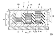
図1に示すように、本実施形態の有機EL装置1は、第1基板2と、第1反射層3と、波長変換層4と、陽極5と、有機層6と、陰極7と、バンドパスフィルター8と、隔壁9と、第2基板10と、封止層11と、を備える。波長変換層4は、緑色波長変換層4Gと、赤色波長変換層4Rと、を含む。陽極5と有機層6と陰極7とは、所定の色光、例えば青色光を発光する発光部12を構成する。本実施形態の第1基板2は、特許請求の範囲の基材に対応する。個々の構成要件の詳細な構成については、後述する。
As shown in FIG. 1, the organic EL device 1 according to this embodiment includes a
本実施形態の有機EL装置1は、表示装置として用いることを想定している。そのため、有機EL装置1は、マトリクス状に配列された複数の画素PXを有する。画素PXは、赤色の表示を行う赤色サブ画素13Rと、緑色の表示を行う緑色サブ画素13Gと、青色の表示を行う青色サブ画素13Bと、から構成されている。図1では、複数の画素のうち、赤色サブ画素13Rと緑色サブ画素13Gと青色サブ画素13Bとからなる一つの画素PXのみを代表して図示している。
The organic EL device 1 of this embodiment is assumed to be used as a display device. Therefore, the organic EL device 1 has a plurality of pixels PX arranged in a matrix. The pixel PX is composed of a
ただし、有機EL装置1の用途は必ずしも表示装置に限ることはなく、例えば照明装置等の用途で用いられてもよい。また、有機EL装置1は、必ずしも複数の異なる色の光を射出するものでなくてもよく、単色の光を射出するものであってもよい。 However, the use of the organic EL device 1 is not necessarily limited to the display device, and may be used, for example, for a lighting device or the like. The organic EL device 1 may not necessarily emit light of a plurality of different colors, and may emit monochromatic light.
第1基板2には、例えば、ガラス、石英等からなる無機材料基板、ポリエチレンテレフタレート、ポリカルバゾール、ポリイミド等を含むプラスティック基板、アルミナ等を含むセラミックス基板等の絶縁性基板、もしくは、アルミニウム(Al)、鉄(Fe)等を含む金属基板、または、基板上に酸化シリコン(SiO2)、有機絶縁材料等を含む絶縁物を表面にコーティングした基板、Al等を含む金属基板の表面を陽極酸化等の方法で絶縁化処理を施した基板等を用いることができる。なお、本実施形態で使用できる第1基板2は、これらの基板に限定されるものではない。
As the
例えば第1基板2の材料をガラスとした場合、高温プロセスによっても変形が起こらず、水分を透過させないため、有機層6の劣化が抑えられる点で好適である。第2基板10についても、第1基板2と同様の基板を用いることができる。ただし、第1基板2は光透過性を有していなくてもよいが、第2基板10は表示装置の観察者に向けて光を透過させなければならないため、光透過性を有する基板でなければならない。
For example, when the material of the
図1では図示を省略したが、第1基板2の第2基板10と対向する側の面(図1における第1基板2の上側の面)に、TFT回路が設けられている。TFT回路は、発光部12のスイッチング用素子および駆動用素子として機能する。TFT回路の具体的な構成としては、公知のTFT回路を用いることができる。以下の説明においては、第1基板2の第2基板10と対向する側の面を、第1基板2の第1面2aと称する。
Although not shown in FIG. 1, a TFT circuit is provided on the surface of the
第1反射層3は、第1基板2の第1面2a(有機層6および波長変換層4と第1基板2との間)に設けられている。第1反射層3は、発光部12から発せられて第1基板2に向けて進む光を第2基板10側に向けて反射する。第1反射層3は、後述する陰極7とは異なり、光透過性を有する必要はない。そのため、第1反射層3には、光反射率が高い材料が好適に用いられる。本実施形態では、第1反射層3の材料として、例えば光を透過させないだけの膜厚を有するAl膜が用いられる。第1反射層3は、青色波長域の光の少なくとも一部、緑色波長域の光の少なくとも一部、および赤色波長域の光の少なくとも一部を反射する特性を有する必要がある。
本実施形態の青色波長域は、特許請求の範囲の第1波長域に対応する。本実施形態の緑色波長域および赤色波長域は、特許請求の範囲の第2波長域に対応する。
The first
The blue wavelength range in the present embodiment corresponds to the first wavelength range in the claims. The green wavelength range and the red wavelength range in the present embodiment correspond to the second wavelength range in the claims.
発光部12は、陽極5と、陰極7と、陽極5と陰極7との間に挟持された有機層6と、を備える。有機層6は、例えば正孔注入層15、正孔輸送層16、発光体層17、電子輸送層18、電子注入層19の5つの層が陽極5側から陰極7側に向けて順に積層された構成を有する。陽極5は、第1基板2の第1面2aの側に設けられている。陰極7は、第1基板2の第1面2aの側であって、有機層6および波長変換層4の第1基板2とは反対側に設けられている。発光部12は、波長変換層4に含有される蛍光体材料の励起光となる青色光を射出する。
The
本実施形態の陽極5は、特許請求の範囲の第1電極に相当する。本実施形態の陰極7は、特許請求の範囲の第2電極および第2反射層に相当する。すなわち、本実施形態の陰極7は、第2電極と第2反射層とを兼ねている。ただし、陰極7は、必ずしも第2電極と第2反射層とを兼ねていなくてもよい。発光部12は、陰極7とは別に第2反射層を備えていてもよい。一方、本実施形態の陽極5は、第1電極と第1反射層とを兼ねていないが、第1電極と第1反射層とを兼ねていてもよい。
The
有機層6は、本実施形態の構成に限定されず、少なくとも発光体層17を含んでいればよい。すなわち、有機層6は、発光体層17の単層構造であってもよいし、発光体層17と正孔輸送層16もしくは電子輸送層18等を含む多層構造であってもよい。有機層6は、例えば下記の9種類のうちのいずれかの構成を有することができるが、本発明の有機EL装置はこれらにより限定されるものではない。
(1)発光体層
(2)発光体層/正孔輸送層
(3)電子輸送層/発光体層
(4)電子輸送層/発光体層/正孔輸送層
(5)電子輸送層/発光体層/正孔輸送層/正孔注入層
(6)電子注入層/電子輸送層/発光体層/正孔輸送層/正孔注入層
(7)電子輸送層/正孔防止層/発光体層/正孔輸送層/正孔注入層
(8)電子注入層/電子輸送層/正孔防止層/発光体層/正孔輸送層/正孔注入層
(9)電子注入層/電子輸送層/正孔防止層/発光体層/電子防止層/正孔輸送層/正孔注入層
ここで、発光体層、正孔注入層、正孔輸送層、正孔防止層、電子防止層、電子輸送層および電子注入層の各層は、単層構造でも多層構造でもよい。
The
(1) Light emitter layer
(2) Light emitter layer / hole transport layer (3) electron transport layer / light emitter layer (4) electron transport layer / light emitter layer / hole transport layer (5) electron transport layer / light emitter layer / hole transport Layer / hole injection layer (6) electron injection layer / electron transport layer / light emitter layer / hole transport layer / hole injection layer (7) electron transport layer / hole blocking layer / light emitter layer / hole transport layer / Hole injection layer (8) electron injection layer / electron transport layer / hole blocking layer / light emitter layer / hole transport layer / hole injection layer (9) electron injection layer / electron transport layer / hole blocking layer / Light emitting layer / electron blocking layer / hole transporting layer / hole injecting layer Here, light emitting layer, hole injecting layer, hole transporting layer, hole blocking layer, electron blocking layer, electron transporting layer and electron injecting layer Each of these layers may have a single layer structure or a multilayer structure.
発光体層17は、以下に例示する有機発光材料のみから構成されていてもよく、発光性のドーパントおよびホスト材料の組み合わせから構成されていてもよく、任意に正孔輸送材料、電子輸送材料、添加剤(ドナー、アクセプター等)等を含んでいてもよく、これらの材料が高分子材料(結着用樹脂)または無機材料中に分散された構成であってもよい。発光効率および発光寿命の観点からは、ホスト材料中に発光性のドーパントが分散されたものが好ましい。
The
有機発光材料としては、有機EL用の公知の発光材料を挙げることができる。この種の発光材料は、低分子発光材料、高分子発光材料等に分類され、これらの具体的な化合物を以下に例示するが、本発明はこれらの材料に限定されるものではない。有機発光材料として、蛍光材料、燐光材料等に分類されるものを用いることができる。低消費電力化の観点で、発光効率の高い燐光材料を用いてもよい。 As an organic luminescent material, the well-known luminescent material for organic EL can be mentioned. Light emitting materials of this type are classified into low molecular weight light emitting materials, high molecular weight light emitting materials and the like, and specific compounds thereof are exemplified below, but the present invention is not limited to these materials. As the organic light emitting material, those classified into fluorescent materials, phosphorescent materials and the like can be used. From the viewpoint of reducing power consumption, a phosphorescent material with high luminous efficiency may be used.
具体的な化合物を以下に例示するが、本発明はこれらの化合物に限定されるものではない。
低分子有機発光材料としては、例えば、4,4’−ビス(2,2’−ジフェニルビニル)−ビフェニル(DPVBi)等の芳香族ジメチリデン化合物、5−メチル−2−[2−[4−(5−メチル−2−ベンゾオキサゾリル)フェニル]ビニル]ベンゾオキサゾール等のオキサジアゾール化合物、3−(4−ビフェニルイル)−4−フェニル−5−t−ブチルフェニル−1,2,4−トリアゾール(TAZ)等のトリアゾール誘導体、1,4−ビス(2−メチルスチリル)ベンゼン等のスチリルベンゼン化合物、フルオレノン誘導体等の蛍光性有機材料等が挙げられる。
Specific compounds are exemplified below, but the present invention is not limited to these compounds.
Examples of the low-molecular organic light-emitting material include aromatic dimethylidene compounds such as 4,4′-bis (2,2′-diphenylvinyl) -biphenyl (DPVBi), 5-methyl-2- [2- [4- ( Oxadiazole compounds such as 5-methyl-2-benzoxazolyl) phenyl] vinyl] benzoxazole, 3- (4-biphenylyl) -4-phenyl-5-t-butylphenyl-1,2,4- Examples include triazole derivatives such as triazole (TAZ), styrylbenzene compounds such as 1,4-bis (2-methylstyryl) benzene, and fluorescent organic materials such as fluorenone derivatives.
高分子発光材料としては、例えば、ポリ(2−デシルオキシ−1,4−フェニレン)(DO−PPP)、等のポリフェニレンビニレン誘導体、ポリ(9,9−ジオクチルフルオレン)(PDAF)等のポリスピロ誘導体が挙げられる。 Examples of the polymer light-emitting material include polyphenylene vinylene derivatives such as poly (2-decyloxy-1,4-phenylene) (DO-PPP), and polyspiro derivatives such as poly (9,9-dioctylfluorene) (PDAF). Can be mentioned.
発光体層21に任意に含まれる発光性のドーパントとしては、有機EL素子用の公知のドーパント材料を挙げることができる。このようなドーパント材料として、例えば、スチリル誘導体等の蛍光発光材料、ビス[(4,6−ジフルオロフェニル)−ピリジナト−N,C2’]ピコリネートイリジウム(III)(FIrpic)、ビス(4’,6‘−ジフルオロフェニルポリジナト)テトラキス(1−ピラゾイル)ボレートイリジウム(III)(FIr6)等の燐光発光有機金属錯体等が挙げられる。 Examples of the light emitting dopant optionally contained in the light emitting layer 21 include known dopant materials for organic EL devices. Examples of such dopant materials include fluorescent materials such as styryl derivatives, bis [(4,6-difluorophenyl) -pyridinato-N, C2 ′] picolinate iridium (III) (FIrpic), bis (4 ′, 6'-Difluorophenylpolydinato) phosphorescent organometallic complexes such as tetrakis (1-pyrazolyl) borate iridium (III) (FIr6) and the like can be mentioned.
ドーパントを使用する際のホスト材料としては、有機EL素子用の公知のホスト材料を挙げることができる。このようなホスト材料としては、上述した低分子発光材料、高分子発光材料、4,4’−ビス(カルバゾール)ビフェニル、9,9−ジ(4−ジカルバゾール−ベンジル)フルオレン(CPF)、3,6−ビス(トリフェニルシリル)カルバゾール(mCP)、(PCF)等のカルバゾール誘導体、4−(ジフェニルフォスフォイル)−N,N−ジフェニルアニリン(HM−A1)等のアニリン誘導体、1,3−ビス(9−フェニル−9H−フルオレン−9−イル)ベンゼン(mDPFB)、1,4−ビス(9−フェニル−9H−フルオレン−9−イル)ベンゼン(pDPFB)等のフルオレン誘導体等が挙げられる。 Examples of the host material when using the dopant include known host materials for organic EL elements. As such a host material, the above-described low molecular light emitting material, polymer light emitting material, 4,4′-bis (carbazole) biphenyl, 9,9-di (4-dicarbazole-benzyl) fluorene (CPF), 3 , 6-bis (triphenylsilyl) carbazole (mCP), carbazole derivatives such as (PCF), aniline derivatives such as 4- (diphenylphosphoyl) -N, N-diphenylaniline (HM-A1), 1,3- And fluorene derivatives such as bis (9-phenyl-9H-fluoren-9-yl) benzene (mDPFB) and 1,4-bis (9-phenyl-9H-fluoren-9-yl) benzene (pDPFB).
電荷は、正孔と電子とを含む。陽極5から発光体層17への正孔の注入および輸送をより効率良く行なう目的で、正孔注入層15および正孔輸送層16が用いられる。陰極7から発光体層17への電子の注入および輸送をより効率良く行なう目的で、電子注入層19および電子輸送層18が用いられる。これらの層は、以下に例示する電荷注入・輸送材料のみから構成されていてもよく、任意に添加剤(ドナー、アクセプター等)等を含んでいてもよく、これらの材料が高分子材料(結着用樹脂)または無機材料中に分散された構成であってもよい。
The charge includes holes and electrons. In order to more efficiently inject and transport holes from the
電荷注入・輸送材料としては、有機EL素子用、有機光導電体用の公知のものを使用することができる。このような電荷注入輸送材料は、正孔注入・輸送材料および電子注入・輸送材料に分類され、これらの具体的な化合物を以下に例示するが、本発明はこれらの材料に限定されるものではない。 As the charge injection / transport material, known materials for organic EL devices and organic photoconductors can be used. Such charge injecting and transporting materials are classified into hole injecting and transporting materials and electron injecting and transporting materials, and these specific compounds are exemplified below, but the present invention is not limited to these materials. Absent.
正孔注入層15および正孔輸送層16の材料としては、例えば、酸化バナジウム(V2O5)、酸化モリブデン(MoO2)等の酸化物、無機p型半導体材料、ポルフィリン化合物、N,N’−ビス(3−メチルフェニル)−N,N’−ビス(フェニル)−ベンジジン(TPD)、N,N’−ジ(ナフタレン−1−イル)−N,N’−ジフェニル−ベンジジン(NPD)等の芳香族第三級アミン化合物、ヒドラゾン化合物、キナクリドン化合物、スチリルアミン化合物等の低分子材料、ポリアニリン(PANI)、ポリアニリン−樟脳スルホン酸(PANI−CSA)、3,4−ポリエチレンジオキシチオフェン/ポリスチレンサルフォネイト(PEDOT/PSS)、ポリ(トリフェニルアミン)誘導体(Poly−TPD)、ポリビニルカルバゾール(PVCz)、ポリ(p−フェニレンビニレン)(PPV)、ポリ(p−ナフタレンビニレン)(PNV)等の高分子材料等が挙げられる。
Examples of the material for the
陽極5からの正孔の注入および輸送をより効率良く行なうという観点から、正孔注入層15の材料として、正孔輸送層16の材料との最高被占分子軌道(HOMO)のエネルギー障壁が小さい材料を用いることが好ましい。
From the viewpoint of more efficient injection and transport of holes from the
正孔の注入性および輸送性をより向上させるため、材料にアクセプターをドープすることが好ましい。アクセプターとしては、有機EL素子用の公知のアクセプター材料を使用することができる。これらの具体的な化合物を以下に例示するが、本発明はこれらの材料に限定されるものではない。 In order to further improve the injectability and transportability of holes, it is preferable to dope the material with an acceptor. As an acceptor, the well-known acceptor material for organic EL elements can be used. Although these specific compounds are illustrated below, this invention is not limited to these materials.
アクセプター材料としては、Au、Pt、W,Ir、POCl3、AsF6、Cl、Br、I、酸化バナジウム(V2O5)、酸化モリブデン(MoO2)等の無機材料、TCNQ(7,7,8,8,−テトラシアノキノジメタン)、TCNQF4(テトラフルオロテトラシアノキノジメタン)、TCNE(テトラシアノエチレン)、HCNB(ヘキサシアノブタジエン)、DDQ(ジシクロジシアノベンゾキノン)等のシアノ基を有する化合物、TNF(トリニトロフルオレノン)、DNF(ジニトロフルオレノン)等のニトロ基を有する化合物、フルオラニル、クロラニル、ブロマニル等の有機材料が挙げられる。このうち、TCNQ、TCNQF4、TCNE、HCNB、DDQ等のシアノ基を有する化合物は、キャリア濃度を効果的に増加させることができるため、より好ましい。 Acceptor materials include Au, Pt, W, Ir, POC 13 , AsF 6 , Cl, Br, I, vanadium oxide (V 2 O 5 ), molybdenum oxide (MoO 2 ) and other inorganic materials, TCNQ (7, 7 , 8, 8-tetracyanoquinodimethane), TCNQF 4 (tetrafluorotetracyanoquinodimethane), TCNE (tetracyanoethylene), HCNB (hexacyanobutadiene), DDQ (dicyclodicyanobenzoquinone), etc. And compounds having a nitro group such as TNF (trinitrofluorenone) and DNF (dinitrofluorenone), and organic materials such as fluoranyl, chloranil and bromanyl. Among these, compounds having a cyano group such as TCNQ, TCNQF 4 , TCNE, HCNB, DDQ and the like are more preferable because they can effectively increase the carrier concentration.
電子注入層19および電子輸送層18の材料としては、例えば、n型半導体である無機材料、オキサジアゾール誘導体、トリアゾール誘導体、チオピラジンジオキシド誘導体、ベンゾキノン誘導体、ナフトキノン誘導体、アントラキノン誘導体、ジフェノキノン誘導体、フルオレノン誘導体、ベンゾジフラン誘導体等の低分子材料;ポリ(オキサジアゾール)(Poly−OXZ)、ポリスチレン誘導体(PSS)等の高分子材料等が使用される。特に電子注入層19の材料には、フッ化リチウム(LiF)、フッ化バリウム(BaF2)等のフッ化物、酸化リチウム(Li2O)等の酸化物等が挙げられる。
Examples of materials for the
陰極7からの電子の注入・輸送をより効率良く行なうという観点から、電子注入層19の材料としては、電子輸送層18の材料との最低空分子軌道(LUMO)のエネルギー障壁が小さい材料を用いることが望ましい。
From the viewpoint of performing electron injection / transport from the
電子の注入効率および電子の輸送性をより向上させるため、電子注入層19および電子輸送層18の材料に、ドナーをドープすることが好ましい。ドナーとしては、有機EL素子用の公知のドナー材料を使用することができる。これらの具体的な化合物を以下に例示するが、本発明はこれらの材料に限定されるものではない。
In order to further improve the electron injection efficiency and the electron transportability, it is preferable to dope the material of the
ドナー材料としては、アルカリ金属、アルカリ土類金属、希土類元素、Al、Ag、Cu、In等の無機材料、アニリン類、フェニレンジアミン類、ベンジジン類(N,N,N’,N’−テトラフェニルベンジジン、N,N’−ビス−(3−メチルフェニル)−N,N’−ビス−(フェニル)−ベンジジン、N,N’−ジ(ナフタレン−1−イル)−N,N’−ジフェニル−ベンジジン等)、トリフェニルアミン類(トリフェニルアミン、4,4’,4”−トリス(N,N−ジフェニル−アミノ)−トリフェニルアミン、4,4’,4”−トリス(N−3−メチルフェニル−N−フェニル−アミノ)−トリフェニルアミン、4,4’,4”−トリス(N−(1−ナフチル)−N−フェニル−アミノ)−トリフェニルアミン等)、トリフェニルジアミン類(N,N’−ジ−(4−メチル−フェニル)−N,N’−ジフェニル−1,4−フェニレンジアミン)等の芳香族3級アミンを骨格にもつ化合物、フェナントレン、ピレン、ペリレン、アントラセン、テトラセン、ペンタセン等の縮合多環化合物(ただし、縮合多環化合物は置換基を有してもよい)、TTF(テトラチアフルバレン)類、ジベンゾフラン、フェノチアジン、カルバゾール等の有機材料がある。このうち、芳香族3級アミンを骨格にもつ化合物、縮合多環化合物、アルカリ金属は、キャリア濃度を効果的に増加させることができるため、より好ましい。 Donor materials include inorganic materials such as alkali metals, alkaline earth metals, rare earth elements, Al, Ag, Cu, and In, anilines, phenylenediamines, benzidines (N, N, N ′, N′-tetraphenyl) Benzidine, N, N′-bis- (3-methylphenyl) -N, N′-bis- (phenyl) -benzidine, N, N′-di (naphthalen-1-yl) -N, N′-diphenyl- Benzidine, etc.), triphenylamines (triphenylamine, 4,4 ′, 4 ′ ′-tris (N, N-diphenyl-amino) -triphenylamine, 4,4 ′, 4 ′ ′-tris (N-3-3) Methylphenyl-N-phenyl-amino) -triphenylamine, 4,4 ', 4' '-tris (N- (1-naphthyl) -N-phenyl-amino) -triphenylamine etc.), triphenyldia Compounds having an aromatic tertiary amine skeleton such as N (N, N′-di- (4-methyl-phenyl) -N, N′-diphenyl-1,4-phenylenediamine), phenanthrene, pyrene, perylene And condensed polycyclic compounds such as anthracene, tetracene and pentacene (however, the condensed polycyclic compound may have a substituent), TTF (tetrathiafulvalene) s, organic materials such as dibenzofuran, phenothiazine and carbazole. Among these, compounds having an aromatic tertiary amine in the skeleton, condensed polycyclic compounds, and alkali metals are more preferable because the carrier concentration can be effectively increased.
正孔注入層15、正孔輸送層16、発光体層17、電子輸送層18および電子注入層19等を含む有機層6は、上述したこれらの層の材料を溶剤に溶解、分散させた発光層形成用塗液を用いて形成できる。このとき、スピンコーティング法、ディッピング法、ドクターブレード法、吐出コート法、スプレーコート法等の塗布法、インクジェット法、凸版印刷法、凹版印刷法、スクリーン印刷法、マイクログラビアコート法等の印刷法等による公知のウエットプロセス、上記の材料を抵抗加熱蒸着法、電子線(EB)蒸着法、分子線エピタキシー(MBE)法、スパッタリング法、有機気相蒸着(OVPD)法等の公知のドライプロセス、または、レーザー転写法等が用いられる。ウエットプロセスにより有機層6を形成する場合、発光層形成用塗液は、レベリング剤、粘度調整剤等の塗液の物性を調整するための添加剤を含んでいてもよい。
The
陽極5および陰極7を形成する電極材料としては、公知の電極材料を使用することができる。陽極5を形成する電極材料としては、有機層6への正孔の注入をより効率良く行なえる観点から、仕事関数が4.5eV以上の金(Au)、白金(Pt)、ニッケル(Ni)等の金属、および、インジウム(In)および錫(Sn)を含む酸化物(ITO)、錫(Sn)の酸化物(SnO2)、インジウム(In)および亜鉛(Zn)を含む酸化物(IZO)等が透明電極材料として挙げられる。陰極7を形成する電極材料としては、有機層6への電子の注入をより効率良く行なえる観点から、仕事関数が4.5eV以下のリチウム(Li)、カルシウム(Ca)、セリウム(Ce)、バリウム(Ba)、アルミニウム(Al)等の金属、または、これらの金属を含有するMg:Ag合金、Li:Al合金等の合金が挙げられる。
A known electrode material can be used as an electrode material for forming the
陽極5および陰極7のうち、光を取り出す側に位置する電極は、発光体層17から発せられる光の少なくとも一部を透過させるものでなければならない。本実施形態では、発光体層17から発せられた光を第2基板10側、すなわち陰極7側から取り出す。本実施形態の陰極7は、青色波長域の光の少なくとも一部、緑色波長域の光の少なくとも一部、および赤色波長域の光の少なくとも一部を反射し、緑色波長域の光の他の一部、および赤色波長域の光の他の一部を透過する特性を有する。本実施形態では、陰極7の材料として、例えば所望の光透過率を確保できるだけの膜厚を有するMg:Ag合金膜が用いられる。
Of the
陽極5は、陰極7とは異なり、反射層を兼ねていない。そのため、陽極7は、光反射性を有する必要はなく、光透過率が高い材料が好適に用いられる。本実施形態では、陽極5の材料として、例えばIZO膜が用いられる。なお、陽極5−陰極7間の各層の積層順を本実施形態とは逆にして、陽極5側から光を取り出し、陰極7側で光を反射させる構成を採用してもよい。
Unlike the
本実施形態の有機EL装置1において、緑色サブ画素13Gに緑色波長変換層4Gが設けられ、赤色サブ画素13Rには赤色波長変換層4Rが設けられている。青色サブ画素13Gには波長変換層が設けられていない。発光部12から射出された青色光は、これら波長変換層4G,4Rに入射し、蛍光体材料の励起光として機能する。緑色サブ画素13Gの緑色波長変換層4Gに入射した青色光は、緑色光に波長変換されて射出される。赤色サブ画素13Rの赤色波長変換層4Rに入射した青色光は、赤色光に波長変換されて射出される。青色サブ画素13Bに入射した青色光は、波長変換されることなく射出される。
In the organic EL device 1 of the present embodiment, the green
緑色波長変換層4Gは、第1反射層3と陽極5との間に設けられている。赤色波長変換層4Rは、第1反射層3と陽極5との間に設けられている。すなわち、緑色波長変換層4Gおよび赤色波長変換層4Rは、陽極5と陰極7とで挟まれる発光部12の外側に設けられている。
The green
緑色波長変換層4Gおよび赤色波長変換層4Rは、以下に例示する蛍光体材料のみから構成されていてもよく、添加剤等を含んでいてもよく、これらの材料が高分子材料(結着用樹脂)または無機材料中に分散された構成であってもよい。本実施形態の緑色波長変換層4Gおよび赤色波長変換層4Rは、例えば透明樹脂中に複数の蛍光体粒子21G,21Rが分散された構成を有する。蛍光体粒子21G,21Rは、青色光の照射により緑色もしくは赤色の蛍光を生じる蛍光体材料で構成されている。透明樹脂には、例えばPMMA(ポリメチルメタクリレート)、PVA(ポリビニルアルコール)等の材料が用いられる。
The green
緑色波長変換層4Gに含まれる蛍光体粒子21Gには、公知の蛍光体材料を使用することができる。このような蛍光体材料は、有機系蛍光体材料と無機系蛍光体材料に分類され、これらの具体的な化合物を以下に例示するが、本発明はこれらの材料に限定されるものではない。
A known phosphor material can be used for the
有機系蛍光体材料の場合、青色光を緑色光に変換する蛍光色素として、クマリン系色素:2,3,5,6−1H、4H−テトラヒドロ−8−トリフロメチルキノリジン(9,9a、1−gh)クマリン(クマリン153)、3−(2′−ベンゾチアゾリル)―7−ジエチルアミノクマリン(クマリン6)、3−(2′−ベンゾイミダゾリル)―7−N,N−ジエチルアミノクマリン(クマリン7)、ナフタルイミド系色素:ベーシックイエロー51、ソルベントイエロー11、ソルベントイエロー116等が挙げられる。 In the case of an organic phosphor material, as a fluorescent dye that converts blue light into green light, a coumarin dye: 2,3,5,6-1H, 4H-tetrahydro-8-trifluoromethylquinolidine (9,9a, 1-gh) Coumarin (coumarin 153), 3- (2'-benzothiazolyl) -7-diethylaminocoumarin (coumarin 6), 3- (2'-benzoimidazolyl) -7-N, N-diethylaminocoumarin (coumarin 7), Naphthalimide dyes: basic yellow 51, solvent yellow 11, solvent yellow 116 and the like.
無機系蛍光体材料の場合、青色光を緑色光に変換する蛍光材料として、(BaMg)Al16O27:Eu2+,Mn2+、Sr4Al14O25:Eu2+、(SrBa)Al12Si2O8:Eu2+、(BaMg)2SiO4:Eu2+、Y2SiO5:Ce3+,Tb3+、Sr2P2O7−Sr2B2O5:Eu2+、(BaCaMg)5(PO4)3Cl:Eu2+、Sr2Si3O8−2SrCl2:Eu2+、Zr2SiO4、MgAl11O19:Ce3+,Tb3+、Ba2SiO4:Eu2+、Sr2SiO4:Eu2+、(BaSr)SiO4:Eu2+等が挙げられる。 In the case of an inorganic phosphor material, (BaMg) Al 16 O 27 : Eu 2+ , Mn 2+ , Sr 4 Al 14 O 25 : Eu 2+ , (SrBa) Al 12 Si are used as fluorescent materials that convert blue light into green light. 2 O 8 : Eu 2+ , (BaMg) 2 SiO 4 : Eu 2+ , Y 2 SiO 5 : Ce 3+ , Tb 3+ , Sr 2 P 2 O 7- Sr 2 B 2 O 5 : Eu 2+ , (BaCaMg) 5 ( PO 4 ) 3 Cl: Eu 2+ , Sr 2 Si 3 O 8 -2SrCl 2 : Eu 2+ , Zr 2 SiO 4 , MgAl 11 O 19 : Ce 3+ , Tb 3+ , Ba 2 SiO 4 : Eu 2+ , Sr 2 SiO 4 : Eu 2+, (BaSr) SiO 4 : include Eu 2+ and the like.
赤色波長変換層4Rに含まれる蛍光体粒子21Rには、公知の蛍光体材料を使用することができる。このような蛍光体材料は、有機系蛍光体材料と無機系蛍光体材料に分類され、これらの具体的な化合物を以下に例示するが、本発明はこれらの材料に限定されるものではない。
A known phosphor material can be used for the
有機系蛍光体材料としては、青色光を赤色光に変換する蛍光色素として、シアニン系色素:4−ジシアノメチレン−2−メチル−6−(p−ジメチルアミノスチルリル)−4H−ピラン、ピリジン系色素:1−エチル−2−[4−(p−ジメチルアミノフェニル)−1,3−ブタジエニル]−ピリジニウム−パークロレート、およびローダミン系色素:ローダミンB、ローダミン6G、ローダミン3B、ローダミン101、ローダミン110、ベーシックバイオレット11、スルホローダミン101等が挙げられる。
Examples of organic phosphor materials include cyanine dyes: 4-dicyanomethylene-2-methyl-6- (p-dimethylaminostyryl) -4H-pyran, pyridine dyes as fluorescent dyes that convert blue light into red light Dye: 1-ethyl-2- [4- (p-dimethylaminophenyl) -1,3-butadienyl] -pyridinium-perchlorate, and rhodamine dyes: rhodamine B, rhodamine 6G, rhodamine 3B, rhodamine 101, rhodamine 110 ,
無機系蛍光体材料としては、青色光を赤色光に変換する蛍光体として、Y2O2S:Eu3+、YAlO3:Eu3+、Ca2Y2(SiO4)6:Eu3+、LiY9(SiO4)6O2:Eu3+、YVO4:Eu3+、CaS:Eu3+、Gd2O3:Eu3+、Gd2O2S:Eu3+、Y(P,V)O4:Eu3+、Mg4GeO5.5F:Mn4+、Mg4GeO6:Mn4+、K5Eu2.5(WO4)6.25、Na5Eu2.5(WO4)6.25、K5Eu2.5(MoO4)6.25、Na5Eu2.5(MoO4)6.25等が挙げられる。 As the inorganic phosphor material, Y 2 O 2 S: Eu 3+ , YAlO 3 : Eu 3+ , Ca 2 Y 2 (SiO 4 ) 6: Eu 3+ , LiY 9 are used as phosphors that convert blue light into red light. (SiO 4 ) 6 O 2 : Eu 3+ , YVO 4 : Eu 3+ , CaS: Eu 3+ , Gd 2 O 3 : Eu 3+ , Gd 2 O 2 S: Eu 3+ , Y (P, V) O 4 : Eu 3+ , Mg 4 GeO 5 . 5 F: Mn 4+ , Mg 4 GeO 6 : Mn 4+ , K 5 Eu 2.5 (WO 4 ) 6.25 , Na 5 Eu 2.5 (WO 4 ) 6.25 , K 5 Eu 2.5 (MoO 4 ) 6.25 , Na 5 Eu 2.5 (MoO 4 ) 6.25 and the like.
緑色波長変換層4Gおよび赤色波長変換層4Rは、上記の蛍光体材料と樹脂材料とを溶剤に溶解、分散させた蛍光体層形成用塗液を用いて形成される。このとき、スピンコーティング法、ディッピング法、ドクターブレード法、吐出コート法、スプレーコート法等の塗布法、インクジェット法、凸版印刷法、凹版印刷法、スクリーン印刷法、マイクログラビアコート法等の印刷法等による公知のウエットプロセス、抵抗加熱蒸着法、電子線(EB)蒸着法、分子線エピタキシー(MBE)法、スパッタリング法、有機気相蒸着(OVPD)法等の公知のドライプロセス、または、レーザー転写法等が用いられる。
The green
緑色サブ画素13Gにおいて、陰極7の有機層6とは反対側(陰極7の上方)にバンドパスフィルター8が設けられている。赤色サブ画素13Rにおいて、陰極7の有機層6とは反対側(陰極7の上方)にバンドパスフィルター8が設けられている。青色サブ画素13Gにはバンドパスフィルターが設けられていない。これらのバンドパスフィルター8は、例えば屈折率が異なる誘電体膜が交互に多数積層された誘電体多層膜により構成されている。
In the
緑色サブ画素13Gのバンドパスフィルター8は、青色光を反射し、緑色光を透過する特性を有する。緑色サブ画素13Gのバンドパスフィルター8は、必ずしも青色光の全てを反射し、緑色光の全てを透過しなくてもよく、青色光の少なくとも一部を反射し、緑色光の少なくとも一部を透過すればよい。赤色サブ画素13Rのバンドパスフィルター8は、青色光を反射し、赤色光を透過する特性を有する。赤色サブ画素13Gのバンドパスフィルター8は、必ずしも青色光の全てを反射し、赤色光の全てを透過しなくてもよく、青色光の少なくとも一部を反射し、赤色光の少なくとも一部を透過すればよい。
The
第2基板10は、封止基板として機能する。第2基板10は、例えばガラス、石英等からなる無機材料基板、ポリエチレンテレフタレート、ポリカルバゾール、ポリイミド等を含むプラスティック基板等の光透過率が高い材料からなる基板が好適に用いられる。ただし、本実施形態で用いられる第2基板10は、これらの基板に限定されるものではない。
The
第2基板10と陰極7もしくはバンドパスフィルター8との間に、封止層11が設けられている。封止層11は、各サブ画素13B,13G,13Rの構成部材を封止し、水分等の浸入を防止する。封止層11は、任意の絶縁材料を用いて形成することができる。絶縁材料は、有機材料、無機材料のいずれであってもよい。
A
隔壁9は、隣り合うサブ画素間を区画するように、第2基板10側から見て格子状に設けられている。隔壁9の断面形状は、図1に示すように、第1基板2の側から第2基板10の側に向けて同一の幅を有していてもよいし、幅が変化していてもよい。すなわち、隔壁9の断面形状は、テーパ状であってもよい。隔壁9の材料には、光透過性材料もしくは遮光性材料が用いられてもよいし、光反射性材料が用いられてもよい。
The
蛍光は、蛍光体粒子21G,21Rを中心として等方的に発せられる。ここで、テーパ状の隔壁9に光反射性材料を用いた場合、蛍光体粒子21G,21Rから発せられた蛍光のうち、隔壁9に向かって進む光が隔壁9の側面で反射して方向を変え、第2基板10に向けて進む。これにより、蛍光の取り出し効率を高めることができる。この観点から、隔壁9の断面形状を第2基板の10側で狭く、第1基板2の側で広いテーパ状とし、隔壁9の材料に光反射性材料が用いられることが好ましい。その場合であっても、必ずしも隔壁9の全体が光反射性材料で構成されていなくてもよく、少なくとも隔壁9の側面が光反射性材料で構成されていればよい。
The fluorescence is emitted isotropically around the
本実施形態の有機EL装置1は、マイクロキャビティ効果を発現する共振器構造を有する。マイクロキャビティ効果を発現するためには、例えば一対の反射層間に存在する層全体の厚さを、増強させたい光の波長に応じて設定する。共振器構造として、第2反射層として機能する陰極7と第1反射層3との間に、青色サブ画素13Bにおいては陽極5および有機層6が設けられ、緑色サブ画素13Gにおいては緑色波長変換層4G、陽極5および有機層6が設けられ、赤色サブ画素13Rにおいては赤色波長変換層4R、陽極5および有機層6が設けられている。これら陰極7と第1反射層3との間に存在する複数の膜の合計膜厚を、増強させたい光の波長に応じて設定する。これにより、発光体層17および波長変換層4から発せられた光が第1反射層3と陰極7との間で多重反射を繰り返し、共振することによって、所望の波長の光が増強される。
The organic EL device 1 of the present embodiment has a resonator structure that exhibits a microcavity effect. In order to exhibit the microcavity effect, for example, the thickness of the entire layer present between a pair of reflective layers is set according to the wavelength of light to be enhanced. As the resonator structure, the
以下、本実施形態の有機EL装置1における共振器構造の光学距離について説明する。
特許文献1に記載の発光素子では、マイクロキャビティ構造が、波長変換層から射出された光を強め、励起光を強めないような光学距離を有していた。そのため、励起光が一対の反射層間で反射を繰り返す間に減衰し、波長変換層に吸収される励起光の強度が低下する、という問題があった。そこで、本実施形態の有機EL装置1では、マイクロキャビティ構造が、波長変換層4から射出された光を強めると同時に、発光部12から射出された励起光をも強めるような光学距離に設定されている点が、特許文献1の発光素子と異なる。これにより、励起光の強度が高い状態で波長変換層4に吸収されるため、発光効率に優れた有機EL装置を実現することができる。
Hereinafter, the optical distance of the resonator structure in the organic EL device 1 of the present embodiment will be described.
In the light emitting device described in Patent Document 1, the microcavity structure has an optical distance such that the light emitted from the wavelength conversion layer is intensified and the excitation light is not intensified. Therefore, there is a problem that the excitation light is attenuated while being repeatedly reflected between the pair of reflection layers, and the intensity of the excitation light absorbed by the wavelength conversion layer is reduced. Therefore, in the organic EL device 1 of the present embodiment, the microcavity structure is set to an optical distance that enhances the light emitted from the
具体的には、一対の反射層間の光学距離(本実施形態では第1反射層3と陰極7との間の光学距離)をLとする。有機EL装置1からの出力光を視認する際の視線の角度(画面の法線に対する角度)をθとする。共振波長をλとする。干渉の次数をm(m=1,2,3,…)とする。各反射層で光が反射する際の位相シフトの和をΦ(rad)とする。ここで、一対の反射層間の光学距離Lは、一対の反射層間に存在する層全体の光学膜厚である。言い換えると、一対の反射層間の光学距離Lは、一対の反射層間に存在する複数の層の屈折率と膜厚との積の総和である。例えば一対の反射層間に存在する層が3層であり、第1層の屈折率がn1、第1層の膜厚がd1、第2層の屈折率がn2、第2層の膜厚がd2、第3層の屈折率がn3、第3層の膜厚がd3であったとすると、光学距離Lは、L=n1×d1+n2×d2+n3×d3、と表される。角度θについては、有機EL装置1の正面方向を角度θ=0°とする。
Specifically, an optical distance between the pair of reflective layers (optical distance between the first
このとき、下記の(1)式で示される共振条件が満たされれば、共振波長λの光が共振し、増幅される。2つの発光ピーク波長、例えば波長λ1および波長λ2の双方に対して共振条件を満たすためには、波長λ1、波長λ2のいずれを代入しても(1)式が成立するように、一対の反射層間の光学距離Lを設定すればよい。 At this time, if the resonance condition represented by the following equation (1) is satisfied, the light having the resonance wavelength λ resonates and is amplified. In order to satisfy the resonance condition for both of the two emission peak wavelengths, for example, the wavelength λ1 and the wavelength λ2, a pair of reflections so that the equation (1) is satisfied regardless of which of the wavelengths λ1 and λ2 is substituted. The optical distance L between layers may be set.
![]()
![]()
緑色サブ画素13Gにおいて、第1反射層3と陰極7との間の光学距離Lは、2つの異なる波長λ1,λ2の光である青色光と緑色光のいずれに対しても共振条件を満たす光学距離に略一致している。青色光の共振波長λ1を例えば442nmとし、緑色光の共振波長λ2を例えば510nmとしたとき、青色光と緑色光のいずれに対しても共振条件を満たす光学距離Lは、(1)式から、例えば1657.5nmとなる。
In the
赤色サブ画素13Rにおいて、第1反射層3と陰極7との間の光学距離Lは、2つの異なる波長λ1,λ2の光である青色光と赤色光のいずれに対しても共振条件を満たす光学距離に略一致している。青色光の共振波長λ1を例えば442nmとし、赤色光の共振波長λ2を例えば598nmとしたとき、青色光と赤色光のいずれに対しても共振条件を満たす光学距離Lは、(1)式から、例えば2541.5nmとなる。
In the
青色サブ画素13Bにおいて、第1反射層3と陰極7との間の光学距離Lは、青色光のみに対して共振条件を満たす光学距離に略一致している。青色光の共振波長λ1を例えば442nmとしたとき、青色光に対して共振条件を満たす光学距離Lは、(1)式から、例えば552.5nmとなる。
In the
第1反射層3と陰極7との間に存在する各層の膜厚および光学膜厚(nd:屈折率と膜厚との積)を[表1]に示す。[表1]では、第1反射層3と陰極7との間の電子注入層を除く有機層6の部分はまとめて示した。
Table 1 shows the film thickness and optical film thickness (nd: product of refractive index and film thickness) of each layer existing between the first

(1)式中の位相シフトをΦ=2πとすると、緑色サブ画素13Gについては、[表1]に示すように、波長λ1=442nmにおいて、角度θ=0°、次数m=15、光学距離L=1657.5nmのとき、(1)式は成立する。また、波長λ2=510nmにおいて、角度θ=0°、次数m=13、光学距離L=1657.5nmのとき、(1)式は成立する。
Assuming that the phase shift in the equation (1) is Φ = 2π, for the
赤色サブ画素13Rについては、[表1]に示すように、波長λ1=442nmにおいて、角度θ=0°、次数m=23、光学距離L=2541.5nmのとき、(1)式は成立する。また、波長λ2=598nmにおいて、角度θ=0°、次数m=17、光学距離L=2541.5nmのとき、(1)式は成立する。
青色サブ画素13Bについては、[表1]に示すように、波長λ=442nmにおいて、角度θ=0°、次数m=5、光学距離L=552.5nmのとき、(1)式は成立する。
For the
For the
陽極5から陰極7までの各層の構成材料および膜厚は、全てのサブ画素にわたって共通としている。そのため、本実施形態の場合、異なる色のサブ画素毎に最適な光学距離Lを異ならせるために、波長変換層4の膜厚を異ならせている。具体的には、緑色サブ画素13Gにおいては、緑色波長変換層4Gの膜厚を650nm(光学膜厚:nd=1105nm)としている。これに対して、赤色サブ画素13Rについては、赤色波長変換層4Rの膜厚を1170nm(光学膜厚:nd=1989nm)としている。
The constituent material and film thickness of each layer from the
従来の波長変換方式の有機EL装置には、励起光を発光する有機EL発光部と波長変換層とが別々の基板に設けられた構成の有機EL装置が存在していた。この種の有機EL装置では、有機EL発光部から波長変換層までの距離が長くなり、有機EL発光部から射出される励起光のロスが多くなる。また、励起光のロスを補うために波長変換層を厚くする必要がある、という問題があった。 In conventional wavelength conversion type organic EL devices, organic EL devices having a configuration in which an organic EL light emitting unit that emits excitation light and a wavelength conversion layer are provided on different substrates exist. In this type of organic EL device, the distance from the organic EL light emitting unit to the wavelength conversion layer becomes long, and the loss of excitation light emitted from the organic EL light emitting unit increases. There is also a problem that the wavelength conversion layer needs to be thickened to compensate for the loss of excitation light.
これに対して、本実施形態の有機EL装置1においては、発光部12が設けられた第1基板2上に波長変換層4が設けられ、発光部12と波長変換層4とが隣り合っているため、励起光のロスを十分に小さくすることができる。また、励起光のロスが少ないため、波長変換層4の膜厚が薄くて済む、という効果が得られる。
On the other hand, in the organic EL device 1 of the present embodiment, the
また、本実施形態の有機EL装置1においては、緑色サブ画素13Gもしくは赤色サブ画素13Rにおける第1反射層3−陰極7間の光学距離Lが、励起光である青色光と波長変換層4から射出される波長変換光の双方に対して共振条件を満たす光学距離に略一致している。そのため、発光部12から射出された青色光がマイクロキャビティ構造内で共振し、増強されて波長変換層4の蛍光体材料に吸収され、さらに波長変換層4からの波長変換光がマイクロキャビティ構造内で共振し、増強される。
Further, in the organic EL device 1 of the present embodiment, the optical distance L between the first
マイクロキャビティ構造の光射出側には、各サブ画素に対応したバンドパスフィルター8が設けられているため、青色光はバンドパスフィルター8で反射され、マイクロキャビティ構造内に閉じ込められる。そのため、増強された青色光は、視認側に射出されることがなく、波長変換層4の励起光として十分に機能を果たす。一方、波長変換光はバンドパスフィルター8を透過し、増強された波長変換光は、視認側に射出される。このように、本実施形態によれば、発光効率に優れた有機EL装置1を実現することができる。
Since the
[第2実施形態]
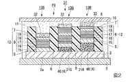
以下、本発明の第2実施形態について、図2を用いて説明する。
図2は、第2実施形態の有機EL装置の断面図である。
第2実施形態の有機EL装置の基本構成は第1実施形態と同様であり、光散乱層を備えた点が第1実施形態と異なる。
図2において、第1実施形態で用いた図1と共通の構成要素には同一の符号を付し、詳細な説明は省略する。
Second Embodiment
Hereinafter, a second embodiment of the present invention will be described with reference to FIG.
FIG. 2 is a cross-sectional view of the organic EL device of the second embodiment.
The basic configuration of the organic EL device of the second embodiment is the same as that of the first embodiment, and is different from the first embodiment in that a light scattering layer is provided.
In FIG. 2, the same components as those in FIG. 1 used in the first embodiment are denoted by the same reference numerals, and detailed description thereof is omitted.
図2に示すように、第2実施形態の有機EL装置31は、各サブ画素13B,13G,13Rにおける発光部12の光射出側に光散乱層32を備えている。すなわち、青色サブ画素13Bにおいて、光散乱層32は、陰極7の光射出側(図2における上方)に陰極7と接するように積層されている。緑色サブ画素13Gにおいて、光散乱層32は、バンドパスフィルター8の光射出側(図2における上方)にバンドパスフィルター8と接するように積層されている。赤色サブ画素13Rにおいて、光散乱層32は、バンドパスフィルター8の光射出側にバンドパスフィルター8と接するように積層されている。光散乱層32には、例えば基材の内部に基材の屈折率とは異なる屈折率の微粒子を分散させた部材、あるいは表面に微細な凹凸が設けられた部材、などが用いられる。
As shown in FIG. 2, the
青色サブ画素13Bにおいて、光散乱層32は、発光部12から射出された青色光を透過しつつ散乱させる。緑色サブ画素13Gおよび赤色サブ画素13Rにおいて、光散乱層32は、バンドパスフィルター8から射出された波長変換光を透過しつつ散乱させる。
その他の構成は、第1実施形態の有機EL装置と同様である。
In the
The other configuration is the same as that of the organic EL device of the first embodiment.
第2実施形態においても、発光効率に優れた有機EL装置を実現できる、といった第1実施形態と同様の効果が得られる。特に、第2実施形態の有機EL装置31は光散乱層32を備えたことにより、広い視野角にわたって明るい表示が可能な有機EL装置を実現できる。
Also in the second embodiment, the same effect as in the first embodiment can be obtained that an organic EL device having excellent luminous efficiency can be realized. In particular, by providing the
[第3実施形態]
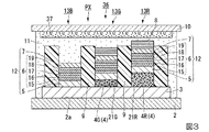
以下、本発明の第3実施形態について、図3を用いて説明する。
図3は、第3実施形態の有機EL装置の断面図である。
第3実施形態の有機EL装置の基本構成は第1実施形態と同様であり、光散乱層を備えた点が第1実施形態と異なる。
図3において、第1実施形態で用いた図1と共通の構成要素には同一の符号を付し、詳細な説明は省略する。
Third Embodiment
Hereinafter, a third embodiment of the present invention will be described with reference to FIG.
FIG. 3 is a cross-sectional view of the organic EL device of the third embodiment.
The basic configuration of the organic EL device of the third embodiment is the same as that of the first embodiment, and is different from the first embodiment in that a light scattering layer is provided.
In FIG. 3, the same components as those in FIG. 1 used in the first embodiment are denoted by the same reference numerals, and detailed description thereof is omitted.
第2実施形態の有機EL装置は、各サブ画素における発光部上に光散乱層が積層されていた。これに対し、図3に示すように、第3実施形態の有機EL装置36において、光散乱層37は、第2基板10の第1基板2との対向面に、第2基板10の略全域にわたって設けられている。光散乱層37の構成は、第2実施形態の有機EL装置と同様である。その他の構成は、第1実施形態の有機EL装置と同様である。
In the organic EL device of the second embodiment, the light scattering layer is stacked on the light emitting portion in each subpixel. On the other hand, as shown in FIG. 3, in the
第3実施形態においても、発光効率に優れた有機EL装置を実現できる、といった第1実施形態と同様の効果が得られる。また、広い視野角にわたって明るい表示が可能な有機EL装置を実現できる、といった第2実施形態と同様の効果が得られる。さらに第3実施形態の場合、第2基板10の略全面に光散乱層37が形成されるため、有機EL装置の製造プロセスが簡単になる。
Also in the third embodiment, an effect similar to that of the first embodiment that an organic EL device excellent in luminous efficiency can be realized is obtained. Moreover, the same effect as 2nd Embodiment that the organic electroluminescent apparatus which can perform bright display over a wide viewing angle is realizable is acquired. Furthermore, in the case of the third embodiment, since the
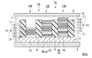
[第4実施形態]
以下、本発明の第4実施形態について、図4を用いて説明する。
図4は、第4実施形態の有機EL装置の断面図である。
第4実施形態の有機EL装置の基本構成は第1実施形態と同様であり、第2基板にカラーフィルターが付加された点が第1実施形態と異なる。
図4において、第1実施形態で用いた図1と共通の構成要素には同一の符号を付し、詳細な説明は省略する。
Fourth Embodiment
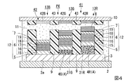
Hereinafter, a fourth embodiment of the present invention will be described with reference to FIG.
FIG. 4 is a cross-sectional view of the organic EL device of the fourth embodiment.
The basic configuration of the organic EL device of the fourth embodiment is the same as that of the first embodiment, and is different from the first embodiment in that a color filter is added to the second substrate.
In FIG. 4, the same components as those in FIG. 1 used in the first embodiment are denoted by the same reference numerals, and detailed description thereof is omitted.
図4に示すように、第4実施形態の有機EL装置41においては、第2基板10の第1基板2に対向する側の面に、カラーフィルター42が設けられている。青色サブ画素13B、緑色サブ画素13Gおよび赤色サブ画素13Rに対応して、青色カラーフィルター42B、緑色カラーフィルター42Gおよび赤色カラーフィルター42Rがそれぞれ設けられている。また、第2基板10の第1基板2に対向する側の面には、各色のカラーフィルター42B,42G,42Rを区画する隔壁43が設けられている。
As shown in FIG. 4, in the
第4実施形態においても、発光効率に優れた有機EL装置を実現できる、といった第1実施形態と同様の効果が得られる。さらに第4実施形態の場合、青色サブ画素13Bにおいて、陰極7から射出された青色光は、青色カラーフィルター42Bを透過して視認側に射出される。緑色サブ画素13Gにおいて、バンドパスフィルター8から射出された緑色光は、緑色カラーフィルター42Gを透過して視認側に射出される。同様に、赤色サブ画素13Rにおいて、バンドパスフィルター8から射出された赤色光は、赤色カラーフィルター42Rを透過して視認側に射出される。このようにして、各サブ画素13B,13G,13Rから射出される光の色純度を高めることができる。
Also in the fourth embodiment, the same effect as in the first embodiment that an organic EL device excellent in luminous efficiency can be realized is obtained. Furthermore, in the case of the fourth embodiment, in the
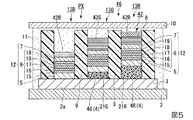
[第5実施形態]
以下、本発明の第5実施形態について、図5を用いて説明する。
図5は、第5実施形態の有機EL装置の断面図である。
第5実施形態の有機EL装置の基本構成は第1実施形態と同様であり、カラーフィルターを備えた点が第1実施形態と異なる。
図5において、第1実施形態で用いた図1と共通の構成要素には同一の符号を付し、詳細な説明は省略する。
Fifth Embodiment
Hereinafter, a fifth embodiment of the present invention will be described with reference to FIG.
FIG. 5 is a cross-sectional view of the organic EL device of the fifth embodiment.
The basic configuration of the organic EL device of the fifth embodiment is the same as that of the first embodiment, and is different from the first embodiment in that a color filter is provided.
In FIG. 5, the same components as those in FIG. 1 used in the first embodiment are denoted by the same reference numerals, and detailed description thereof is omitted.
第4実施形態の有機EL装置は、第2基板の一面にカラーフィルターが設けられていた。これに対し、図5に示すように、第5実施形態の有機EL装置46は、各サブ画素13B,13G,13Rにおける発光部12の光射出側に、カラーフィルター42を備えている。すなわち、青色カラーフィルター42Bは、青色サブ画素13Bの陰極7の光射出側(図5における上方)に、陰極7と接するように積層されている。緑色カラーフィルター42Gは、緑色サブ画素13Gのバンドパスフィルター8の光射出側(図5における上方)に、バンドパスフィルター8と接するように積層されている。赤色カラーフィルター42Rは、赤色サブ画素13Rのバンドパスフィルター8の光射出側に、バンドパスフィルター8と接するように積層されている。その他の構成は、第1実施形態の有機EL装置と同様である。
In the organic EL device of the fourth embodiment, the color filter is provided on one surface of the second substrate. On the other hand, as shown in FIG. 5, the
第5実施形態においても、発光効率に優れた有機EL装置を実現できる、といった第1実施形態と同様の効果が得られる。さらに、第4実施形態と同様、射出される光の色純度を高めることができる。 Also in the fifth embodiment, the same effect as in the first embodiment that an organic EL device excellent in luminous efficiency can be realized is obtained. Furthermore, as in the fourth embodiment, the color purity of the emitted light can be increased.
[第6実施形態]
以下、本発明の第6実施形態について、図6を用いて説明する。
図6は、第6実施形態の有機EL装置の断面図である。
第6実施形態の有機EL装置の基本構成は第1実施形態と同様であり、光学距離調整層を付加した点が第1実施形態と異なる。
図6において、第1実施形態で用いた図1と共通の構成要素には同一の符号を付し、詳細な説明は省略する。
Sixth Embodiment
Hereinafter, a sixth embodiment of the present invention will be described with reference to FIG.
FIG. 6 is a cross-sectional view of the organic EL device of the sixth embodiment.
The basic configuration of the organic EL device of the sixth embodiment is the same as that of the first embodiment, and is different from the first embodiment in that an optical distance adjustment layer is added.
In FIG. 6, the same components as those in FIG. 1 used in the first embodiment are denoted by the same reference numerals, and detailed description thereof is omitted.
図6に示すように、第6実施形態の有機EL装置51において、光学距離調整層52は、青色サブ画素13Bには設けられておらず、緑色サブ画素13Gと赤色サブ画素13Rとに設けられている。このように、光学距離調整層52は、必ずしも全てのサブ画素に設けられている必要はなく、一部のサブ画素には設けられていなくてもよい。
As shown in FIG. 6, in the
緑色サブ画素13Gおよび赤色サブ画素13Rにおいて、光学距離調整層52は、第1反射層3と陽極5との間に設けられている。具体的には、緑色サブ画素13Gの光学距離調整層52は、第1反射層3と緑色波長変換層4Gとの間に設けられている。赤色サブ画素13Rの光学距離調整層52は、第1反射層3と赤色波長変換層4Rとの間に設けられている。緑色サブ画素13Gの光学距離調整層52と赤色サブ画素13Rの光学距離調整層52とは、膜厚が互いに異なる。
In the
光学距離調整層52は、第1反射層3と陰極7との間の光学距離を調整するために用いられる。例えば光学距離調整層52がなかったとしても、第1反射層3と陰極7との間に存在する他の層の膜厚を調整することにより、第1反射層3と陰極7との間の光学距離を調整することができる。例えば第1実施形態のように、波長変換層4の膜厚をサブ画素毎に調整することにより、第1反射層3と陰極7との間の光学距離を調整してもよい。しかしながら、光学距離調整層52以外の層は、要求される特性上の制約、もしくは製造プロセス上の制約等があり、膜厚を自由に調整するのが難しい場合がある。そのため、第6実施形態の有機EL装置51は、光学距離調整層52を備えている。
The optical
光学距離調整層52は、発光体層17から発せられた光を第1反射層3に向けて透過させ、第1反射層3で反射した光を発光体層17に向けて再度透過させる。そのため、光学距離調整層52には、光透過率が高く、膜厚が自由に調整しやすい材料が好適に用いられる。第6実施形態では、光学距離調整層52の材料として、例えば無機物(SiO2、SiON、SiN等)や有機物(ポリカーボネート、ポリアクリレート、シリコーン樹脂等)の絶縁膜や透明導電性材料等のいずれを用いてもよい。
The optical
光学距離調整層52に用いられる無機絶縁材料としては、従来知られている種々の金属酸化物、金属窒化物、金属フッ化物などを用いることができる。
金属酸化物の具体例としては、MgO、SiO、SiO2、Al2O3、GeO、NiO、CaO、BaO、Fe2O3、Y2O3、TiO2等が挙げられ、金属窒化物の具体例としては、AlN、SiNx、SiNxOy等が挙げられ、金属フッ化物の具体例としては、MgF2、LiF、AlF3、CaF2等が挙げられる。また、これらの混合物であってもよい。
As the inorganic insulating material used for the optical
Specific examples of the metal oxides, MgO, SiO, SiO 2, Al 2
光学距離調整層52として有機化合物を用いてもよく、例えば被膜形成性ポリマーが好ましく用いられる。被膜形成性ポリマーとしては、ポリカーボネート、ポリアクリレート、シリコーン樹脂、ポリビニルブチラール等が挙げられる。光学距離調整層52として透明導電性材料を用いてもよく、透明電極を使用してもよい。例えば、インジウム(In)および錫(Sn)を含む酸化物(ITO)、錫(Sn)の酸化物(SnO2)、インジウム(In)および亜鉛(Zn)を含む酸化物(IZO)等が透明電極材料として挙げられる。
An organic compound may be used as the optical
光学距離調整層52の形成方法については、特に限定はなく、例えば真空蒸着法、スパッタリング法、反応性スパッタリング法、MBE(分子線エピタキシー)法、クラスターイオンビーム法、イオンプレーティング法、プラズマ重合法(高周波励起イオンプレーティング法)、プラズマCVD法、レーザーCVD法、熱CVD法、ガスソースCVD法、コーティング法、印刷法、または転写法を適用できる。
The method for forming the optical
緑色サブ画素13Gにおいて、第1反射層3と陰極7との間の光学距離Lは、青色光と緑色光のいずれに対しても共振条件を満たす光学距離に略一致している。青色光の共振波長λ1を例えば442nmとし、緑色光の共振波長λ2を例えば510nmとしたとき、青色光と緑色光のいずれに対しても共振条件を満たす光学距離Lは、例えば1657.5nmである。
In the
赤色サブ画素13Rにおいて、第1反射層3と陰極7との間の光学距離Lは、青色光と赤色光のいずれに対しても共振条件を満たす光学距離に略一致している。青色光の共振波長λ1を例えば442nmとし、赤色光の共振波長λ2を例えば598nmとしたとき、青色光と赤色光のいずれに対しても共振条件を満たす光学距離Lは、例えば2541.5nmである。
In the
青色サブ画素13Bにおいて、第1反射層3と陰極7との間の光学距離Lは、青色光のみに対して共振条件を満たす光学距離に略一致している。青色光の共振波長λ1を例えば442nmとしたとき、青色光に対して共振条件を満たす光学距離Lは、例えば552.5nmである。
In the
第1反射層3と陰極7との間に存在する各層の膜厚および光学膜厚(nd:屈折率と膜厚との積)を[表2]に示す。[表2]では、第1反射層3と陰極7との間の電子注入層を除く有機層6の部分はまとめて示した。
Table 2 shows the film thickness and optical film thickness (nd: product of refractive index and film thickness) of each layer existing between the first
(1)式の中の位相シフトをΦ=2πとすると、緑色サブ画素13Gについては、[表2]に示すように、波長λ1=442nmにおいて、角度θ=0°、次数m=15、光学距離L=1657.5nmのとき、(1)式は成立する。また、波長λ2=510nmにおいて、角度θ=0°、次数m=13、光学距離L=1657.5nmのとき、(1)式は成立する。
Assuming that the phase shift in the equation (1) is Φ = 2π, for the
赤色サブ画素13Rについては、[表2]に示すように、波長λ1=442nmにおいて、角度θ=0°、次数m=23、光学距離L=2541.5nmのとき、(1)式は成立する。また、波長λ2=598nmにおいて、角度θ=0°、次数m=17、光学距離L=2541.5nmのとき、(1)式は成立する。
青色サブ画素13Bについては、[表2]に示すように、波長λ=442nmにおいて、角度θ=0°、次数m=5、光学距離L=552.5nmのとき、(1)式は成立する。
For the
For the
陽極5から陰極7までの各層の構成材料および膜厚は、全てのサブ画素13B,13G,13Rにわたって共通としている。また、第1実施形態では波長変換層4の膜厚を異ならせたが、第6実施形態では波長変換層4の膜厚を全てのサブ画素13B,13G,13Rにわたって共通にし、光学距離調整層52の膜厚をサブ画素13B,13G,13R毎に異ならせている。
The constituent material and film thickness of each layer from the
具体的には、緑色波長変換層4Gの膜厚および赤色波長変換層4Rの膜厚をともに201nm(光学膜厚:nd=341.7nm)とし、緑色サブ画素13Gにおいては、光学距離調整層52の膜厚を350nm(光学膜厚:nd=1105nm)とし、赤色サブ画素13Rにおいては、光学距離調整層52の膜厚を756nm(光学膜厚:nd=1648nm)としている。
Specifically, the film thickness of the green
第6実施形態においても、発光効率に優れた有機EL装置を実現できる、といった第1実施形態と同様の効果が得られる。さらに、波長変換層4の膜厚をサブ画素に依らずに共通にしたことにより、波長変換層4の形成工程の簡略化を図ることができる。
Also in the sixth embodiment, an effect similar to that of the first embodiment that an organic EL device excellent in luminous efficiency can be realized is obtained. Furthermore, by making the film thickness of the
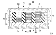
[第7実施形態]
以下、本発明の第7実施形態について、図7を用いて説明する。
図7は、第7実施形態の有機EL装置の断面図である。
第7実施形態の有機EL装置の基本構成は第1実施形態と同様であり、光学距離調整層を付加した点が第1実施形態と異なる。
図7において、第1実施形態で用いた図1と共通の構成要素には同一の符号を付し、詳細な説明は省略する。
Seventh Embodiment
Hereinafter, a seventh embodiment of the present invention will be described with reference to FIG.
FIG. 7 is a cross-sectional view of the organic EL device of the seventh embodiment.
The basic configuration of the organic EL device of the seventh embodiment is the same as that of the first embodiment, and is different from the first embodiment in that an optical distance adjustment layer is added.
In FIG. 7, the same components as those in FIG. 1 used in the first embodiment are denoted by the same reference numerals, and detailed description thereof is omitted.
第6実施形態の有機EL装置では、緑色サブ画素の光学距離調整層は第1反射層と緑色波長変換層との間に設けられ、赤色サブ画素の光学距離調整層は第1反射層と赤色波長変換層との間に設けられていた。これに対して、図7に示すように、第7実施形態の有機EL装置56においては、緑色サブ画素13Gの光学距離調整層52は、緑色波長変換層4Gと陽極5との間に設けられている。赤色サブ画素13Rの光学距離調整層52は、赤色波長変換層4Rと陽極5との間に設けられている。その他の構成は、第6実施形態の有機EL装置と同様である。
In the organic EL device of the sixth embodiment, the optical distance adjustment layer of the green sub-pixel is provided between the first reflection layer and the green wavelength conversion layer, and the optical distance adjustment layer of the red sub-pixel is the first reflection layer and red It was provided between the wavelength conversion layer. On the other hand, as shown in FIG. 7, in the
第7実施形態においても、発光効率に優れた有機EL装置を実現できる、といった第1実施形態と同様の効果が得られる。また、波長変換層4の形成工程の簡略化を図ることができる、といった第6実施形態と同様の効果が得られる。
Also in the seventh embodiment, an effect similar to that of the first embodiment that an organic EL device excellent in luminous efficiency can be realized is obtained. In addition, the same effect as that of the sixth embodiment can be obtained, such that the formation process of the
[第8実施形態]
以下、本発明の第8実施形態について、図8を用いて説明する。
図8は、第8実施形態の有機EL装置の断面図である。
第8実施形態の有機EL装置の基本構成は第1実施形態と同様であり、波長変換層の位置が第1実施形態と異なる。
図8において、第1実施形態で用いた図1と共通の構成要素には同一の符号を付し、詳細な説明は省略する。
Eighth Embodiment
Hereinafter, an eighth embodiment of the present invention will be described with reference to FIG.
FIG. 8 is a cross-sectional view of the organic EL device of the eighth embodiment.
The basic configuration of the organic EL device of the eighth embodiment is the same as that of the first embodiment, and the position of the wavelength conversion layer is different from that of the first embodiment.
In FIG. 8, the same components as those in FIG. 1 used in the first embodiment are denoted by the same reference numerals, and detailed description thereof is omitted.
第1〜第7実施形態の有機EL装置において、波長変換層は、第1反射層と陽極との間に設けられていた。すなわち、波長変換層は、発光部の外側に設けられていた。これに対し、図8に示すように、第8実施形態の有機EL装置61において、波長変換層62は、正孔輸送性を有する材料で構成されている。波長変換層62は、緑色波長変換層62Gと、赤色波長変換層62Rと、を含む。波長変換層62は、陽極5と発光体層17との間に設けられている。すなわち、波長変換層62は、発光部12の内部(陽極5と陰極7との間)に設けられている。正孔輸送層16および正孔注入層15は、設けられていない。
その他の構成は、第1実施形態の有機EL装置と同様である。
In the organic EL devices of the first to seventh embodiments, the wavelength conversion layer is provided between the first reflective layer and the anode. That is, the wavelength conversion layer was provided outside the light emitting unit. On the other hand, as shown in FIG. 8, in the
The other configuration is the same as that of the organic EL device of the first embodiment.
波長変換層が正孔輸送性もしくは電子輸送性を有していない場合、波長変換層が発光部の内部に設けられていると、陽極と陰極との間の距離が大きくなるため、発光部の駆動電力が増大する、という問題が生じる。しかしながら、第8実施形態の場合、波長変換層62が正孔輸送性を有しているため、波長変換層62が正孔輸送層としての機能を果たすことができる。そのため、波長変換層62が発光部12の内部に設けられていても、特に駆動電力が増大する等の問題がなく、発光効率の向上を図ることができる。また、従来の正孔輸送層が不要となることで、有機EL装置の構造および製造プロセスの簡略化が図れる。
When the wavelength conversion layer does not have hole transportability or electron transportability, if the wavelength conversion layer is provided inside the light emitting portion, the distance between the anode and the cathode becomes large. The problem arises that the driving power is increased. However, in the case of the eighth embodiment, since the
[第9実施形態]
以下、本発明の第9実施形態について、図9を用いて説明する。
図9は、第9実施形態の有機EL装置の断面図である。
第9実施形態の有機EL装置の基本構成は第1実施形態と同様であり、波長変換層の位置が第1実施形態と異なる。
図9において、第1実施形態で用いた図1と共通の構成要素には同一の符号を付し、詳細な説明は省略する。
[Ninth embodiment]
Hereinafter, a ninth embodiment of the present invention will be described with reference to FIG.
FIG. 9 is a cross-sectional view of the organic EL device of the ninth embodiment.
The basic configuration of the organic EL device of the ninth embodiment is the same as that of the first embodiment, and the position of the wavelength conversion layer is different from that of the first embodiment.
9, the same code | symbol is attached | subjected to the same component as FIG. 1 used in 1st Embodiment, and detailed description is abbreviate | omitted.
図9に示すように、第9実施形態の有機EL装置66において、波長変換層67は、電子輸送性を有する材料で構成されている。波長変換層67は、緑色波長変換層67Gと、赤色波長変換層67Rと、を含む。波長変換層67は、発光体層17と陰極7との間に設けられている。すなわち、波長変換層67は、発光部12の内部(陽極5と陰極7との間)に設けられている。また、電子輸送層18および電子注入層19は設けられていない。
その他の構成は、第1実施形態の有機EL装置と同様である。
As shown in FIG. 9, in the
The other configuration is the same as that of the organic EL device of the first embodiment.
第9実施形態の場合、波長変換層67が電子輸送性を有しているため、波長変換層67が電子輸送層としての機能を果たすことができる。そのため、波長変換層67が発光部12の内部に設けられていても、特に駆動電力が増大する等の問題がなく、発光効率の向上を図ることができる。また、従来の電子輸送層が不要となることで、有機EL装置の構造および製造プロセスの簡略化が図れる。
In the ninth embodiment, since the
なお、本発明の技術範囲は上記実施形態に限定されるものではなく、本発明の趣旨を逸脱しない範囲において種々の変更を加えることが可能である。
有機EL装置の各種構成要素の数、配置、形状、寸法、構成材料等の具体例については、上記実施形態に限らず、適宜変更が可能である。
The technical scope of the present invention is not limited to the above embodiment, and various modifications can be made without departing from the spirit of the present invention.
Specific examples of the number, arrangement, shape, dimensions, constituent materials, and the like of various components of the organic EL device are not limited to the above-described embodiment, and can be changed as appropriate.
本発明の有機EL装置は、各種の表示装置もしくは照明装置等に利用が可能である。 The organic EL device of the present invention can be used for various display devices or lighting devices.
1,31,36,41,46,51,56,61,66…有機EL装置、2…第1基板(基材)、3…第1反射層、4,62,67…波長変換層、4G,62G,67G…緑色波長変換層、4R,62R,67R…赤色波長変換層、5…陽極(第1電極)、6…有機層、7…陰極(第2電極、第2反射層)、8…バンドパスフィルター、13B…青色サブ画素、13G…緑色サブ画素、13R…赤色サブ画素、32,37…光散乱層、42…カラーフィルター、42B…青色カラーフィルター、42G…緑色カラーフィルター、42R…赤色カラーフィルター、52…光学距離調整層。 1, 3, 36, 41, 46, 51, 56, 61, 66 Organic light emitting device, 2. First substrate (base material), 3. First reflection layer, 4, 62, 67: Wavelength conversion layer, 4G , 62G, 67G ... green wavelength conversion layer, 4R, 62R, 67R ... red wavelength conversion layer, 5 ... anode (first electrode), 6 ... organic layer, 7 ... cathode (second electrode, second reflection layer), 8 ... band pass filter, 13B ... blue sub-pixel, 13G ... green sub-pixel, 13R ... red sub-pixel, 32, 37 ... light scattering layer, 42 ... color filter, 42B ... blue color filter, 42G ... green color filter, 42R ... Red color filter, 52: optical distance adjustment layer.
Claims (8)
前記基材の第1面の側に設けられた第1電極と、
前記基材の前記第1面の側に設けられた第2電極と、
前記第1電極と前記第2電極との間に設けられ、前記第1電極および前記第2電極から電荷の注入により第1波長域の光を発する有機発光層を含む有機層と、
前記基材の第1面の側に設けられ、前記第1波長域の光の少なくとも一部を吸収し、前記第1波長域と異なる第2波長域の光を発する波長変換層と、
前記有機層および前記波長変換層と前記基材との間に設けられ、前記第1電極よりも前記基材側に設けられ、前記第1波長域の光の少なくとも一部および前記第2波長域の光の少なくとも一部を反射する第1反射層と、を備え、
前記第2電極は、前記第1波長域の光の少なくとも一部および前記第2波長域の光の一部を反射し、前記第2波長域の光の他の一部を透過する第2反射層として機能し、
前記第1反射層と前記第2反射層とによって共振器構造が構成され、
前記第1反射層と前記第2反射層との間の光学距離は、前記第1波長域の光および前記第2波長域の光のいずれに対しても共振条件を満たす光学距離に略一致する、有機エレクトロルミネッセンス装置。 A substrate;
A first electrode provided on the side of the first surface of the substrate;
A second electrode provided on the side of the first surface of the substrate;
An organic layer provided between the first electrode and the second electrode, the organic layer including an organic light emitting layer that emits light of a first wavelength range by injection of charges from the first electrode and the second electrode;
A wavelength conversion layer provided on the side of the first surface of the base material, absorbing at least a part of the light in the first wavelength range, and emitting light in a second wavelength range different from the first wavelength range;
It is provided between the organic layer, the wavelength conversion layer, and the substrate, and is provided closer to the substrate than the first electrode, and at least a part of the light in the first wavelength region and the second wavelength region comprising of a first reflecting layer reflecting at least part of the light, and
The second electrode reflects the portion of the at least a portion and said second wavelength band of light before Symbol first wavelength range of light, the second passing through the other part of the second wavelength band of light as a reflective layer function,
A resonator structure is constituted by the first reflective layer and the second reflective layer,
The optical distance between the first reflective layer and the second reflective layer substantially matches the optical distance satisfying the resonance condition for both the light in the first wavelength range and the light in the second wavelength range. Organic electroluminescence device.
Priority Applications (1)
| Application Number | Priority Date | Filing Date | Title |
|---|---|---|---|
| JP2015186898A JP6552100B2 (en) | 2015-09-24 | 2015-09-24 | Organic electroluminescent device |
Applications Claiming Priority (1)
| Application Number | Priority Date | Filing Date | Title |
|---|---|---|---|
| JP2015186898A JP6552100B2 (en) | 2015-09-24 | 2015-09-24 | Organic electroluminescent device |
Publications (2)
| Publication Number | Publication Date |
|---|---|
| JP2017062902A JP2017062902A (en) | 2017-03-30 |
| JP6552100B2 true JP6552100B2 (en) | 2019-07-31 |
Family
ID=58429043
Family Applications (1)
| Application Number | Title | Priority Date | Filing Date |
|---|---|---|---|
| JP2015186898A Active JP6552100B2 (en) | 2015-09-24 | 2015-09-24 | Organic electroluminescent device |
Country Status (1)
| Country | Link |
|---|---|
| JP (1) | JP6552100B2 (en) |
Families Citing this family (6)
| Publication number | Priority date | Publication date | Assignee | Title |
|---|---|---|---|---|
| JP2019102153A (en) | 2017-11-29 | 2019-06-24 | 株式会社ジャパンディスプレイ | Light emitting device and display device |
| CN111903192B (en) * | 2018-03-30 | 2024-09-27 | 索尼半导体解决方案公司 | Display device, method for manufacturing display device, and electronic apparatus |
| KR20250079071A (en) * | 2018-06-06 | 2025-06-04 | 가부시키가이샤 한도오따이 에네루기 켄큐쇼 | Light emitting device, display device, and electronic device |
| CA3131865A1 (en) * | 2019-03-04 | 2020-09-10 | Immunolight, Llc. | Energy augment structures for use with energy emitters and collectors |
| KR102785403B1 (en) | 2020-03-03 | 2025-03-21 | 삼성전자주식회사 | Light emitting device and display apparatus including the light emitting device |
| JP7564966B2 (en) * | 2021-10-13 | 2024-10-09 | シャープ株式会社 | Light-emitting element and light-emitting device |
Family Cites Families (3)
| Publication number | Priority date | Publication date | Assignee | Title |
|---|---|---|---|---|
| JP2008226718A (en) * | 2007-03-14 | 2008-09-25 | Fuji Electric Holdings Co Ltd | Organic EL device |
| JP2010015785A (en) * | 2008-07-02 | 2010-01-21 | Fujifilm Corp | Light-emitting element, multicolor display device, and light-emitting element manufacturing method |
| JP2014165062A (en) * | 2013-02-26 | 2014-09-08 | Sharp Corp | Phosphor substrate and display device |
-
2015
- 2015-09-24 JP JP2015186898A patent/JP6552100B2/en active Active
Also Published As
| Publication number | Publication date |
|---|---|
| JP2017062902A (en) | 2017-03-30 |
Similar Documents
| Publication | Publication Date | Title |
|---|---|---|
| US9182631B2 (en) | Phosphor substrate, display device, and electronic apparatus | |
| JP4654207B2 (en) | Display device | |
| JP5538519B2 (en) | Light emitting element, display and display device | |
| CN102835190B (en) | Fluorophor substrate and manufacture method thereof and display unit | |
| US20150042933A1 (en) | Fluorescent substrate and display device provided with same | |
| JP6552100B2 (en) | Organic electroluminescent device | |
| JP2017037121A (en) | Color conversion substrate and display device | |
| WO2011125363A1 (en) | Organic electroluminescence element, organic electroluminescence display, and organic electroluminescence display apparatus | |
| JP2015064391A (en) | Phosphor substrate, display device, and electronic apparatus | |
| WO2012108384A1 (en) | Fluorescent substrate, and display device and lighting device using same | |
| WO2012090786A1 (en) | Light-emitting device, display device, and illumination device | |
| KR20090092698A (en) | Resonant cavity color conversion el device and organic el display device using the same | |
| JP2016218151A (en) | Wavelength conversion substrate, light emitting device, display device including the same, lighting device, and electronic apparatus | |
| US8823030B2 (en) | Light-emitting device and lighting device | |
| WO2013038971A1 (en) | Light-emitting device, display device and lighting device | |
| WO2015174464A1 (en) | Organic electroluminescence display device | |
| WO2012081568A1 (en) | Fluorescent substrate, display device, and lighting device | |
| JP2016143658A (en) | Light emitting element and display device | |
| WO2011145418A1 (en) | Phosphor display device, and phosphor layer | |
| JP2017004639A (en) | Organic electroluminescence device | |
| WO2012043611A1 (en) | Organic el display device and method for manufacturing same | |
| WO2011102024A1 (en) | Display device | |
| JP2013191464A (en) | Organic electroluminescent element and manufacturing method therefor, liquid crystal display device | |
| WO2012081536A1 (en) | Light-emitting device, display device, electronic apparatus, and illumination device | |
| WO2013094645A1 (en) | Optical substrate and method for manufacturing same, light-emitting element, liquid crystal element, display device, liquid crystal device, and illumination device |
Legal Events
| Date | Code | Title | Description |
|---|---|---|---|
| A621 | Written request for application examination |
Free format text: JAPANESE INTERMEDIATE CODE: A621 Effective date: 20180323 |
|
| A977 | Report on retrieval |
Free format text: JAPANESE INTERMEDIATE CODE: A971007 Effective date: 20190109 |
|
| A131 | Notification of reasons for refusal |
Free format text: JAPANESE INTERMEDIATE CODE: A131 Effective date: 20190115 |
|
| A521 | Request for written amendment filed |
Free format text: JAPANESE INTERMEDIATE CODE: A523 Effective date: 20190206 |
|
| TRDD | Decision of grant or rejection written | ||
| A01 | Written decision to grant a patent or to grant a registration (utility model) |
Free format text: JAPANESE INTERMEDIATE CODE: A01 Effective date: 20190604 |
|
| A61 | First payment of annual fees (during grant procedure) |
Free format text: JAPANESE INTERMEDIATE CODE: A61 Effective date: 20190701 |
|
| R150 | Certificate of patent or registration of utility model |
Ref document number: 6552100 Country of ref document: JP Free format text: JAPANESE INTERMEDIATE CODE: R150 |