JP6549331B2 - Waveguide device and antenna device provided with the waveguide device - Google Patents
Waveguide device and antenna device provided with the waveguide device Download PDFInfo
- Publication number
- JP6549331B2 JP6549331B2 JP2018538899A JP2018538899A JP6549331B2 JP 6549331 B2 JP6549331 B2 JP 6549331B2 JP 2018538899 A JP2018538899 A JP 2018538899A JP 2018538899 A JP2018538899 A JP 2018538899A JP 6549331 B2 JP6549331 B2 JP 6549331B2
- Authority
- JP
- Japan
- Prior art keywords
- waveguide
- conductive
- conductive member
- hole
- wall
- Prior art date
- Legal status (The legal status is an assumption and is not a legal conclusion. Google has not performed a legal analysis and makes no representation as to the accuracy of the status listed.)
- Active
Links
Images


Classifications
-
- H—ELECTRICITY
- H01—ELECTRIC ELEMENTS
- H01P—WAVEGUIDES; RESONATORS, LINES, OR OTHER DEVICES OF THE WAVEGUIDE TYPE
- H01P3/00—Waveguides; Transmission lines of the waveguide type
-
- H—ELECTRICITY
- H01—ELECTRIC ELEMENTS
- H01Q—ANTENNAS, i.e. RADIO AERIALS
- H01Q21/00—Antenna arrays or systems
- H01Q21/06—Arrays of individually energised antenna units similarly polarised and spaced apart
- H01Q21/061—Two dimensional planar arrays
- H01Q21/064—Two dimensional planar arrays using horn or slot aerials
-
- G—PHYSICS
- G01—MEASURING; TESTING
- G01S—RADIO DIRECTION-FINDING; RADIO NAVIGATION; DETERMINING DISTANCE OR VELOCITY BY USE OF RADIO WAVES; LOCATING OR PRESENCE-DETECTING BY USE OF THE REFLECTION OR RERADIATION OF RADIO WAVES; ANALOGOUS ARRANGEMENTS USING OTHER WAVES
- G01S7/00—Details of systems according to groups G01S13/00, G01S15/00, G01S17/00
- G01S7/02—Details of systems according to groups G01S13/00, G01S15/00, G01S17/00 of systems according to group G01S13/00
- G01S7/021—Auxiliary means for detecting or identifying radar signals or the like, e.g. radar jamming signals
-
- G—PHYSICS
- G01—MEASURING; TESTING
- G01S—RADIO DIRECTION-FINDING; RADIO NAVIGATION; DETERMINING DISTANCE OR VELOCITY BY USE OF RADIO WAVES; LOCATING OR PRESENCE-DETECTING BY USE OF THE REFLECTION OR RERADIATION OF RADIO WAVES; ANALOGOUS ARRANGEMENTS USING OTHER WAVES
- G01S7/00—Details of systems according to groups G01S13/00, G01S15/00, G01S17/00
- G01S7/02—Details of systems according to groups G01S13/00, G01S15/00, G01S17/00 of systems according to group G01S13/00
- G01S7/03—Details of HF subsystems specially adapted therefor, e.g. common to transmitter and receiver
-
- H—ELECTRICITY
- H01—ELECTRIC ELEMENTS
- H01P—WAVEGUIDES; RESONATORS, LINES, OR OTHER DEVICES OF THE WAVEGUIDE TYPE
- H01P1/00—Auxiliary devices
- H01P1/18—Phase-shifters
- H01P1/182—Waveguide phase-shifters
-
- H—ELECTRICITY
- H01—ELECTRIC ELEMENTS
- H01P—WAVEGUIDES; RESONATORS, LINES, OR OTHER DEVICES OF THE WAVEGUIDE TYPE
- H01P3/00—Waveguides; Transmission lines of the waveguide type
- H01P3/12—Hollow waveguides
- H01P3/123—Hollow waveguides with a complex or stepped cross-section, e.g. ridged or grooved waveguides
-
- H—ELECTRICITY
- H01—ELECTRIC ELEMENTS
- H01P—WAVEGUIDES; RESONATORS, LINES, OR OTHER DEVICES OF THE WAVEGUIDE TYPE
- H01P5/00—Coupling devices of the waveguide type
- H01P5/12—Coupling devices having more than two ports
-
- H—ELECTRICITY
- H01—ELECTRIC ELEMENTS
- H01Q—ANTENNAS, i.e. RADIO AERIALS
- H01Q1/00—Details of, or arrangements associated with, antennas
- H01Q1/27—Adaptation for use in or on movable bodies
- H01Q1/32—Adaptation for use in or on road or rail vehicles
-
- H—ELECTRICITY
- H01—ELECTRIC ELEMENTS
- H01Q—ANTENNAS, i.e. RADIO AERIALS
- H01Q13/00—Waveguide horns or mouths; Slot antennas; Leaky-waveguide antennas; Equivalent structures causing radiation along the transmission path of a guided wave
- H01Q13/06—Waveguide mouths
-
- H—ELECTRICITY
- H01—ELECTRIC ELEMENTS
- H01Q—ANTENNAS, i.e. RADIO AERIALS
- H01Q13/00—Waveguide horns or mouths; Slot antennas; Leaky-waveguide antennas; Equivalent structures causing radiation along the transmission path of a guided wave
- H01Q13/06—Waveguide mouths
- H01Q13/065—Waveguide mouths provided with a flange or a choke
-
- H—ELECTRICITY
- H01—ELECTRIC ELEMENTS
- H01Q—ANTENNAS, i.e. RADIO AERIALS
- H01Q21/00—Antenna arrays or systems
Landscapes
- Engineering & Computer Science (AREA)
- Radar, Positioning & Navigation (AREA)
- Remote Sensing (AREA)
- Computer Networks & Wireless Communication (AREA)
- Physics & Mathematics (AREA)
- General Physics & Mathematics (AREA)
- Radar Systems Or Details Thereof (AREA)
- Variable-Direction Aerials And Aerial Arrays (AREA)
- Waveguide Aerials (AREA)
- Waveguides (AREA)
- Waveguide Connection Structure (AREA)
- Control Of Motors That Do Not Use Commutators (AREA)
Description
本開示は、導波路装置および当該導波路装置を備えるアンテナ装置に関する。 The present disclosure relates to a waveguide device and an antenna device provided with the waveguide device.
人工磁気導体を備える導波構造の例が特許文献1から3、ならびに非特許文献1および2に開示されている。人工磁気導体は、自然界には存在しない完全磁気導体(PMC: Perfect Magnetic Conductor)の性質を人工的に実現した構造体である。完全磁気導体は、「表面における磁界の接線成分がゼロになる」という性質を有している。これは、完全導体(PEC: Perfect Electric Conductor)の性質、すなわち、「表面における電界の接線成分がゼロになる」という性質とは反対の性質である。完全磁気導体は、自然界には存在しないが、例えば複数の導電性ロッドの配列のような人工的な構造によって実現され得る。人工磁気導体は、その構造によって定まる特定の周波数帯域において、完全磁気導体として機能する。人工磁気導体は、特定の周波数帯域(伝搬阻止帯域)に含まれる周波数を有する電磁波が人工磁気導体の表面に沿って伝搬することを抑制または阻止する。このため、人工磁気導体の表面は、高インピーダンス面と呼ばれることがある。 Examples of waveguide structures comprising artificial magnetic conductors are disclosed in US Pat. An artificial magnetic conductor is a structure that artificially realizes the properties of a perfect magnetic conductor (PMC) that does not exist in nature. The perfect magnetic conductor has the property that "the tangential component of the magnetic field at the surface is zero". This is the opposite of the property of a perfect conductor (PEC), that is, the property that "the tangential component of the electric field at the surface is zero". A perfect magnetic conductor is not present in nature but can be realized by artificial structures, such as an array of conducting rods, for example. The artificial magnetic conductor functions as a perfect magnetic conductor in a specific frequency band determined by its structure. The artificial magnetic conductor suppresses or blocks the propagation of an electromagnetic wave having a frequency included in a specific frequency band (propagation stop band) along the surface of the artificial magnetic conductor. For this reason, the surface of the artificial magnetic conductor may be called a high impedance surface.
特許文献1から3、ならびに非特許文献1および2に開示されている導波路装置では、行および列方向に配列された複数の導電性ロッドによって人工磁気導体が実現されている。このようなロッドは、ポストまたはピンと呼ばれることもある。これらの導波路装置のそれぞれは、全体として、対向する一対の導電プレートを備えている。一方の導電プレートは、他方の導電プレートの側に突出するリッジと、リッジの両側に位置する人工磁気導体とを有している。リッジの上面(導電性を有する面)は、ギャップを介して、他方の導電プレートの導電性表面に対向している。人工磁気導体の伝搬阻止帯域に含まれる波長を有する電磁波は、この導電性表面とリッジの上面との間の空間(ギャップ)をリッジに沿って伝搬する。
In the waveguide devices disclosed in
特許文献1から3、ならびに非特許文献1および2に開示された導波路構造によれば、従来の中空導波管を用いた場合と比較して、小型のアンテナ装置を実現し得る。しかし、アンテナ装置が小さくなると、各アンテナ素子に給電するための給電路の構築が困難になる。
According to the waveguide structures disclosed in
本開示の実施形態は、小型のアンテナ装置に適した新規な給電構造を有する導波路装置を提供する。 Embodiments of the present disclosure provide a waveguide device having a novel feed structure suitable for small antenna devices.
本開示の一態様に係る導波路装置は、自由空間中における最短の波長がλmである帯域の電磁波の伝搬に用いられる導波路装置であって、導電性表面を有する第1の導電部材であって、第1の貫通孔を有する第1の導電部材と、各々が前記導電性表面に対向する先端部を持つ複数の導電性ロッドを有する第2の導電部材であって、前記第1の貫通孔の軸方向に沿って見たときに前記第1の貫通孔と重なる第2の貫通孔を有する第2の導電部材と、前記第1の貫通孔と前記第2の貫通孔との間の空間の少なくとも一部を囲む導電性の導波壁であって、前記複数の導電性ロッドに囲まれ、前記第1の貫通孔と前記第2の貫通孔との間で前記電磁波を伝搬させる導波壁と、を備える。前記導波壁の高さはλm/2未満である。前記複数の導電性ロッドの内、前記導波壁に隣接する前記導電性ロッドと、前記導波壁の外周との距離はλm/2未満である。 A waveguide device according to an aspect of the present disclosure is a waveguide device used for propagating an electromagnetic wave in a band in which the shortest wavelength in free space is λm, and is a first conductive member having a conductive surface. A second conductive member having a first conductive member having a first through hole and a plurality of conductive rods each having a tip end facing the conductive surface, the first conductive member having a first through hole; A second conductive member having a second through hole overlapping with the first through hole when viewed along the axial direction of the hole, and between the first through hole and the second through hole A conductive waveguide wall surrounding at least a part of a space, which is surrounded by the plurality of conductive rods, and which propagates the electromagnetic wave between the first through hole and the second through hole. And a wave wall. The height of the waveguide wall is less than λm / 2. Among the plurality of conductive rods, the distance between the conductive rod adjacent to the waveguide wall and the outer periphery of the waveguide wall is less than λm / 2.
本開示の実施形態によると、導波壁を介して電磁波を、少なくとも1つの導波層を貫いて伝搬させることができる。その際この導波層の上または下の層には、他の導波層又は励振層を配置することができる。中間の層での不要な伝搬を抑制できるため、導波路装置の設計の自由度を向上させることができる。 According to embodiments of the present disclosure, electromagnetic waves can be propagated through the at least one waveguide layer through the waveguide wall. Other waveguide layers or excitation layers can then be arranged in the layers above or below this waveguide layer. Since unnecessary propagation in the middle layer can be suppressed, the degree of freedom in design of the waveguide device can be improved.
本開示の実施形態を説明する前に、本開示の基礎となった知見を説明する。 Before describing the embodiments of the present disclosure, the findings underlying the present disclosure will be described.
前述の特許文献1および非特許文献1に開示されているリッジ導波路は、人工磁気導体として機能し得るワッフルアイアン構造中に設けられている。このような人工磁気導体を利用するリッジ導波路(以下、WRG:Waffle−iron Ridge waveGuideと称する場合がある。)は、マイクロ波またはミリ波帯において、損失の低いアンテナ給電路を実現できる。
The ridge waveguides disclosed in the
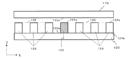
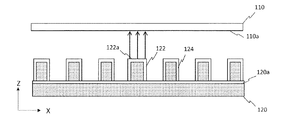
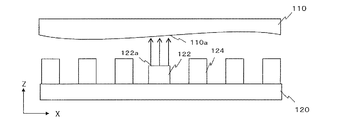
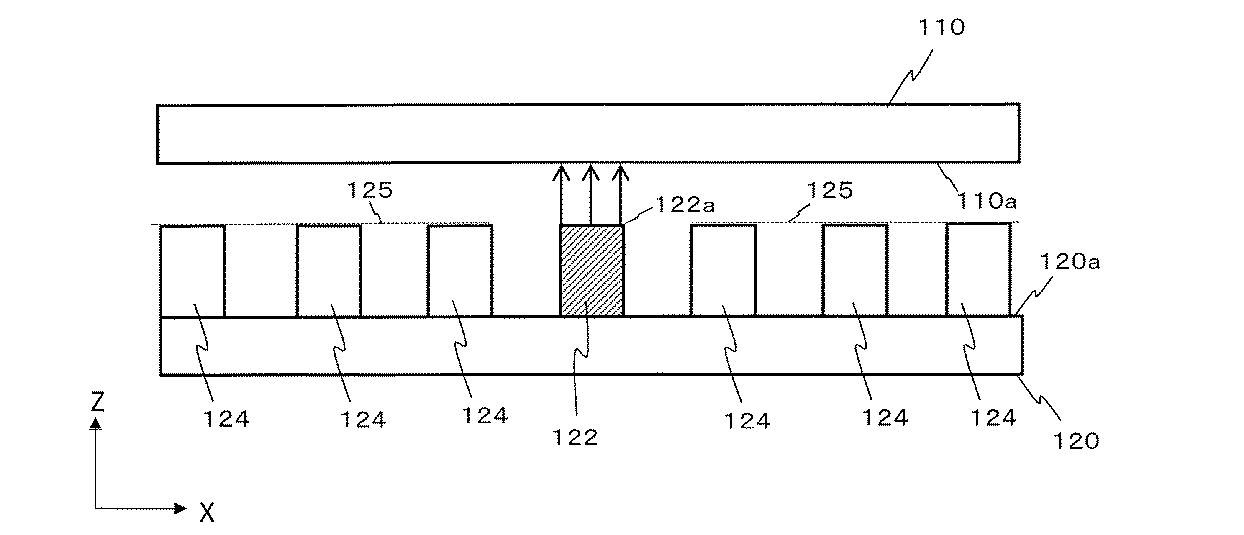
図1は、このような導波路装置が備える基本構成の限定的ではない例を模式的に示す斜視図である。図1では、互いに直交するX、Y、Z方向を示すXYZ座標が示されている。図示されている導波路装置100は、対向して平行に配置されたプレート状の第1の導電部材110および第2の導電部材120を備えている。第2の導電部材120には複数の導電性ロッド124が配列されている。
FIG. 1 is a perspective view schematically showing a non-limiting example of the basic configuration of such a waveguide device. In FIG. 1, XYZ coordinates indicating X, Y, Z directions orthogonal to one another are shown. The illustrated
なお、本願の図面に示される構造物の向きは、説明のわかりやすさを考慮して設定されており、本開示の実施形態が現実に実施されるときの向きをなんら制限するものではない。また、図面に示されている構造物の全体または一部分の形状および大きさも、現実の形状および大きさを制限するものではない。 In addition, the orientation of the structure shown in the drawings of the present application is set in consideration of the ease of explanation, and does not limit the orientation when the embodiment of the present disclosure is actually implemented. In addition, the shape and size of all or a part of the structure shown in the drawings do not limit the actual shape and size.
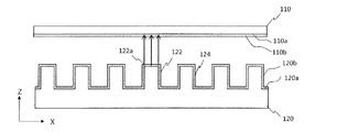
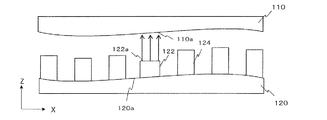
図2Aは、導波路装置100のXZ面に平行な断面の構成を模式的に示す図である。図2Aに示されるように、第1の導電部材110は、第2の導電部材120に対向する側に導電性表面110aを有している。導電性表面110aは、導電性ロッド124の軸方向(Z方向)に直交する平面(XY面に平行な平面)に沿って二次元的に拡がっている。この例における導電性表面110aは平滑な平面であるが、後述するように、導電性表面110aは平面である必要は無い。
FIG. 2A is a view schematically showing the configuration of a cross section parallel to the XZ plane of the
図3は、わかりやすさのため、第1の導電部材110と第2の導電部材120との間隔を極端に離した状態にある導波路装置100を模式的に示す斜視図である。現実の導波路装置100では、図1および図2Aに示したように、第1の導電部材110と第2の導電部材120との間隔は狭く、第1の導電部材110は、第2の導電部材120の全ての導電性ロッド124を覆うように配置されている。
FIG. 3 is a perspective view schematically showing the
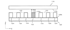
再び図2Aを参照する。第2の導電部材120上に配列された複数の導電性ロッド124は、それぞれ、導電性表面110aに対向する先端部124aを有している。図示されている例において、複数の導電性ロッド124の先端部124aは同一平面上にある。この平面は人工磁気導体の表面125を形成している。導電性ロッド124は、その全体が導電性を有している必要はなく、ロッド状構造物の少なくとも上面および側面に沿って広がる導電層があればよい。この導電層はロッド状構造物の表層に位置してもよいが、表層が絶縁塗装または樹脂層からなり、ロッド状構造物の表面には導電層が存在していない状態であってもよい。また、第2の導電部材120は、複数の導電性ロッド124を支持して人工磁気導体を実現できれば、その全体が導電性を有している必要はない。第2の導電部材120の表面のうち、複数の導電性ロッド124が配列されている側の面120aが導電性を有し、隣接する複数の導電性ロッド124の表面が導電体によって電気的に接続されていればよい。また、導電部材120の導電性を有する層は、絶縁塗装または樹脂層で覆われていてもよい。言い換えると、第2の導電部材120および複数の導電性ロッド124の組み合わせの全体は、第1の導電部材110の導電性表面110aに対向する凹凸状の導電層を有していればよい。
Refer again to FIG. 2A. The plurality of
第2の導電部材120上には、複数の導電性ロッド124の間にリッジ状の導波部材122が配置されている。より詳細には、導波部材122の両側にそれぞれ人工磁気導体が位置しており、導波部材122は両側の人工磁気導体によって挟まれている。図3からわかるように、この例における導波部材122は、第2の導電部材120に支持され、Y方向に直線的に延びている。図示されている例において、導波部材122は、導電性ロッド124の高さおよび幅と同一の高さおよび幅を有している。後述するように、導波部材122の高さおよび幅は、導電性ロッド124の高さおよび幅とは異なる値を有していてもよい。導波部材122は、導電性ロッド124とは異なり、導電性表面110aに沿って電磁波を案内する方向(この例ではY方向)に延びている。導波部材122も、全体が導電性を有している必要は無く、第1の導電部材110の導電性表面110aに対向する導電性の導波面122aを有していればよい。第2の導電部材120、複数の導電性ロッド124、および導波部材122は、連続した単一構造体の一部であってもよい。さらに、第1の導電部材110も、この単一構造体の一部であってもよい。
A ridge-
導波部材122の両側において、各人工磁気導体の表面125と第1の導電部材110の導電性表面110aとの間の空間は、特定周波数帯域内の周波数を有する電磁波を伝搬させない。そのような周波数帯域は「禁止帯域」と呼ばれる。導波路装置100内を伝搬する電磁波(以下、「信号波」と称することがある。)の周波数(以下、「動作周波数」と称することがある。)が禁止帯域に含まれるように人工磁気導体は設計される。禁止帯域は、導電性ロッド124の高さ、すなわち、隣接する複数の導電性ロッド124の間に形成される溝の深さ、導電性ロッド124の幅、配置間隔、および導電性ロッド124の先端部124aと導電性表面110aとの間隙の大きさによって調整され得る。
The space between the
次に、図4を参照しながら、各部材の寸法、形状、配置等の例を説明する。 Next, with reference to FIG. 4, an example of dimensions, shapes, arrangement, and the like of each member will be described.
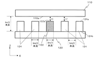
図4は、図2Aに示す構造における各部材の寸法の範囲の例を示す図である。本明細書において、第1の導電部材110の導電性表面110aと導波部材122の導波面122aとの間の導波路を伝搬する電磁波(信号波)の自由空間における波長の代表値(例えば、動作周波数帯域の中心周波数に対応する中心波長)をλoとする。また、動作周波数帯域における最高周波数の電磁波の自由空間における波長をλmとする。各導電性ロッド124のうち、第2の導電部材120に接している方の端の部分を「基部」と称する。図4に示すように、各導電性ロッド124は、先端部124aと基部124bとを有する。各部材の寸法、形状、配置等の例は、以下のとおりである。
FIG. 4 is a view showing an example of a range of dimensions of each member in the structure shown in FIG. 2A. In the present specification, representative values of wavelengths in free space of an electromagnetic wave (signal wave) propagating in the waveguide between the
(1)導電性ロッドの幅
導電性ロッド124の幅(X方向およびY方向のサイズ)は、λm/2未満に設定され得る。この範囲内であれば、X方向およびY方向における最低次の共振の発生を防ぐことができる。なお、XおよびY方向だけでなくXY断面の対角方向でも共振が起こる可能性があるため、導電性ロッド124のXY断面の対角線の長さもλm/2未満であることが好ましい。ロッドの幅および対角線の長さの下限値は、工法的に作製できる最小の長さであり、特に限定されない。
(1) Width of Conductive Rod The width (size in the X direction and the Y direction) of the
(2)導電性ロッドの基部から第1の導電部材の導電性表面までの距離
導電性ロッド124の基部124bから第1の導電部材110の導電性表面110aまでの距離は、導電性ロッド124の高さよりも長く、かつλm/2未満に設定され得る。当該距離がλm/2以上の場合、導電性ロッド124の基部124bと導電性表面110aとの間において共振が生じ、信号波の閉じ込め効果が失われる。
(2) The distance from the base of the conductive rod to the conductive surface of the first conductive member The distance from the base 124 b of the
導電性ロッド124の基部124bから第1の導電部材110の導電性表面110aまでの距離は、第1の導電部材110と第2の導電部材120との間隔に相当する。例えば導波路をミリ波帯である76.5±0.5GHzの信号波が伝搬する場合、信号波の波長は、3.8923mmから3.9435mmの範囲内である。したがって、この場合、λmは3.8923mmとなるので、第1の導電部材110と第2の導電部材120との間隔は、3.8923mmの半分よりも小さく設定され得る。第1の導電部材110と第2の導電部材120とが、このような狭い間隔を実現するように対向して配置されていれば、第1の導電部材110と第2の導電部材120とが厳密に平行である必要はない。また、第1の導電部材110と第2の導電部材120との間隔がλm/2未満であれば、第1の導電部材110および/または第2の導電部材120の全体または一部が曲面形状を有していても良い。他方、第1および第2の導電部材110、120の平面形状(XY面に垂直に投影した領域の形状)および平面サイズ(XY面に垂直に投影した領域のサイズ)は、用途に応じて任意に設計され得る。
The distance from the base 124 b of the
図2Aで示される例において、導電性表面120aは平面であるが、本開示の実施形態はこれに限られない。例えば、図2Bに示すように、導電性表面120aは断面がU字またはV字に近い形状である面の底部であっても良い。導電性ロッド124または導波部材122が、基部に向かって幅が拡大する形状をもつ場合に、導電性表面120aはこのような構造になる。このような構造であっても、導電性表面110aと導電性表面120aとの間の距離が波長λmの半分よりも短ければ、図2Bに示す装置は、本開示の実施形態における導波路装置として機能し得る。
In the example shown in FIG. 2A, the
(3)導電性ロッドの先端部から導電性表面までの距離L2
導電性ロッド124の先端部124aから導電性表面110aまでの距離L2は、λm/2未満に設定される。当該距離がλm/2以上の場合、導電性ロッド124の先端部124aと導電性表面110aとの間を往復する伝搬モードが生じ、電磁波を閉じ込められなくなるからである。なお、複数の導電性ロッド124のうち、少なくとも導波部材122と隣り合うものについては、先端が導電性表面110aとは電気的には接触していない状態にある。ここで、導電性ロッドの先端が導電性表面に電気的に接触していない状態とは、先端と導電性表面との間に空隙がある状態、あるいは、導電性ロッドの先端と導電性表面とのいずれかに絶縁層が存在し、導電性ロッドの先端と導電性表面とが絶縁層を介して接触している状態、のいずれかを指す。
(3) The distance L2 from the tip of the conductive rod to the conductive surface
The distance L2 from the
(4)導電性ロッドの配列および形状
複数の導電性ロッド124のうちの隣接する2つの導電性ロッド124の間の隙間は、例えばλm/2未満の幅を有する。隣接する2つの導電性ロッド124の間の隙間の幅は、当該2つの導電性ロッド124の一方の表面(側面)から他方の表面(側面)までの最短距離によって定義される。このロッド間の隙間の幅は、ロッド間の領域で最低次の共振が起こらないように決定される。共振が生じる条件は、導電性ロッド124の高さ、隣接する2つの導電性ロッド間の距離、および導電性ロッド124の先端部124aと導電性表面110aとの間の空隙の容量の組み合わせによって決まる。よって、ロッド間の隙間の幅は、他の設計パラメータに依存して適宜決定される。ロッド間の隙間の幅には明確な下限はないが、製造の容易さを確保するために、ミリ波帯の電磁波を伝搬させる場合には、例えばλm/16以上であり得る。なお、隙間の幅は一定である必要はない。λm/2未満であれば、導電性ロッド124の間の隙間は様々な幅を有していてもよい。
(4) Arrangement and Shape of Conducting Rods The gap between two adjacent ones of the plurality of
複数の導電性ロッド124の配列は、人工磁気導体としての機能を発揮する限り、図示されている例に限定されない。複数の導電性ロッド124は、直交する行および列状に並んでいる必要は無く、行および列は90度以外の角度で交差していても良い。複数の導電性ロッド124は、行または列に沿って直線上に配列されている必要は無く、単純な規則性を示さずに分散して配置されていても良い。各導電性ロッド124の形状およびサイズも、第2の導電部材120上の位置に応じて変化していて良い。
The arrangement of the plurality of
複数の導電性ロッド124の先端部124aが形成する人工磁気導体の表面125は、厳密に平面である必要は無く、微細な凹凸を有する平面または曲面であってもよい。すなわち、各導電性ロッド124の高さが一様である必要はなく、導電性ロッド124の配列が人工磁気導体として機能し得る範囲内で個々の導電性ロッド124は多様性を持ち得る。
The
導電性ロッド124は、図示されている角柱形状に限らず、例えば円筒状の形状を有していてもよい。さらに、導電性ロッド124は、単純な柱状の形状を有している必要はない。人工磁気導体は、導電性ロッド124の配列以外の構造によっても実現することができ、多様な人工磁気導体を本開示の導波路装置に利用することができる。なお、導電性ロッド124の先端部124aの形状が角柱形状である場合は、その対角線の長さはλm/2未満であることが好ましい。楕円形状であるときは、長軸の長さがλm/2未満であることが好ましい。先端部124aがさらに他の形状をとる場合でも、その差し渡し寸法は一番長い部分でもλm/2未満であることが好ましい。
The
導電性ロッド124の高さ、すなわち、基部124bから先端部124aまでの長さは、導電性表面110aと導電性表面120aとの間の距離(λm/2未満)よりも短い値、例えばλo/4に設定され得る。
The height of
(5)導波面の幅
導波部材122の導波面122aの幅、すなわち、導波部材122が延びる方向に直交する方向における導波面122aのサイズは、λm/2未満(例えばλo/8)に設定され得る。導波面122aの幅がλm/2以上になると、幅方向で共振が起こり、共振が起こるとWRGは単純な伝送線路としては動作しなくなるからである。
(5) Width of Waveguide Surface The width of the
(6)導波部材の高さ
導波部材122の高さ(図示される例ではZ方向のサイズ)は、λm/2未満に設定される。当該距離がλm/2以上の場合、導電性ロッド124の基部124bと導電性表面110aとの距離がλm/2以上となるからである。同様に、導電性ロッド124(特に、導波部材122に隣接する導電性ロッド124)の高さについても、λm/2未満に設定される。
(6) Height of Waveguide Member The height (the size in the Z direction in the illustrated example) of the
(7)導波面と導電性表面との間の距離L1
導波部材122の導波面122aと導電性表面110aとの間の距離L1については、λm/2未満に設定される。当該距離がλm/2以上の場合、導波面122aと導電性表面110aとの間で共振が起こり、導波路として機能しなくなるからである。ある例では、当該距離はλm/4以下である。製造の容易さを確保するために、ミリ波帯の電磁波を伝搬させる場合には、距離L1を、例えばλm/16以上とすることが好ましい。
(7) The distance L1 between the waveguide surface and the conductive surface
The distance L1 between the
導電性表面110aと導波面122aとの距離L1の下限、および導電性表面110aと導電性ロッド124の先端部124aとの距離L2の下限は、機械工作の精度と、上下の2つの導電部材110、120を一定の距離に保つように組み立てる際の精度とに依存する。プレス工法またはインジェクション工法を用いた場合、上記距離の現実的な下限は50マイクロメートル(μm)程度である。MEMS(Micro−Electro−Mechanical System)技術を用いて例えばテラヘルツ領域の製品を作る場合には、上記距離の下限は、2〜3μm程度である。
The lower limit of the distance L1 between the
上記の構成を有する導波路装置100によれば、動作周波数の信号波は、人工磁気導体の表面125と第1の導電部材110の導電性表面110aとの間の空間を伝搬することはできず、導波部材122の導波面122aと第1の導電部材110の導電性表面110aとの間の空間を伝搬する。このような導波路構造における導波部材122の幅は、中空導波管とは異なり、伝搬すべき電磁波の半波長以上の幅を有する必要はない。また、第1の導電部材110と第2の導電部材120とを厚さ方向(YZ面に平行)に延びる金属壁によって接続する必要もない。
According to the
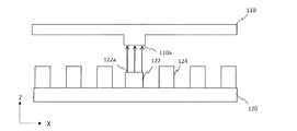
図5Aは、導波部材122の導波面122aと第1の導電部材110の導電性表面110aとの間隙における幅の狭い空間を伝搬する電磁波を模式的に示している。図5Aにおける3本の矢印は、伝搬する電磁波の電界の向きを模式的に示している。伝搬する電磁波の電界は、第1の導電部材110の導電性表面110aおよび導波面122aに対して垂直である。
FIG. 5A schematically shows an electromagnetic wave propagating in a narrow space in the gap between the
導波部材122の両側には、それぞれ、複数の導電性ロッド124によって形成された人工磁気導体が配置されている。電磁波は導波部材122の導波面122aと第1の導電部材110の導電性表面110aとの間隙を伝搬する。図5Aは、模式的であり、電磁波が現実に作る電磁界の大きさを正確には示していない。導波面122a上の空間を伝搬する電磁波(電磁界)の一部は、導波面122aの幅によって区画される空間から外側(人工磁気導体が存在する側)に横方向に拡がっていてもよい。この例では、電磁波は、図5Aの紙面に垂直な方向(Y方向)に伝搬する。このような導波部材122は、Y方向に直線的に延びている必要は無く、不図示の屈曲部および/または分岐部を有し得る。電磁波は導波部材122の導波面122aに沿って伝搬するため、屈曲部では伝搬方向が変わり、分岐部では伝搬方向が複数の方向に分岐する。
Artificial magnetic conductors formed of a plurality of
図5Aの導波路構造では、伝搬する電磁波の両側に、中空導波管では不可欠の金属壁(電気壁)が存在していない。このため、この例における導波路構造では、伝搬する電磁波が作る電磁界モードの境界条件に「金属壁(電気壁)による拘束条件」が含まれず、導波面122aの幅(X方向のサイズ)は、電磁波の波長の半分未満である。
In the waveguide structure of FIG. 5A, the metal wall (electrical wall) which is indispensable in the hollow waveguide does not exist on both sides of the propagating electromagnetic wave. For this reason, in the waveguide structure in this example, the boundary condition of the electromagnetic field mode generated by the propagating electromagnetic wave does not include “restraint condition by metal wall (electric wall)”, and the width (size in the X direction) of the
図5Bは、参考のため、中空導波管130の断面を模式的に示している。図5Bには、中空導波管130の内部空間132に形成される電磁界モード(TE10)の電界の向きが矢印によって模式的に表されている。矢印の長さは電界の強さに対応している。中空導波管130の内部空間132の幅は、波長の半分よりも広く設定されなければならない。すなわち、中空導波管130の内部空間132の幅は、伝搬する電磁波の波長の半分よりも小さく設定され得ない。
FIG. 5B schematically shows a cross section of the
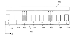
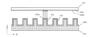
図5Cは、第2の導電部材120上に2個の導波部材122が設けられている形態を示す断面図である。このように隣接する2個の導波部材122の間には、複数の導電性ロッド124によって形成される人工磁気導体が配置されている。より正確には、各導波部材122の両側に複数の導電性ロッド124によって形成される人工磁気導体が配置され、各導波部材122が独立した電磁波の伝搬を実現することが可能である。
FIG. 5C is a cross-sectional view showing an embodiment in which two
図5Dは、参考のため、2つの中空導波管130を並べて配置した導波路装置の断面を模式的に示している。2つの中空導波管130は、相互に電気的に絶縁されている。電磁波が伝搬する空間の周囲が、中空導波管130を構成する金属壁で覆われている必要がある。このため、電磁波が伝搬する内部空間132の間隔を、金属壁の2枚の厚さの合計よりも短縮することはできない。金属壁の2枚の厚さの合計は、通常、伝搬する電磁波の波長の半分よりも長い。したがって、中空導波管130の配列間隔(中心間隔)を、伝搬する電磁波の波長よりも短くすることは困難である。特に、電磁波の波長が10mm以下となるミリ波帯、あるいはそれ以下の波長の電磁波を扱う場合は、波長に比して十分に薄い金属壁を形成することが難しくなる。このため、商業的に現実的なコストで実現することが困難になる。
FIG. 5D schematically shows a cross section of a waveguide device in which two
これに対して、人工磁気導体を備える導波路装置100は、導波部材122を近接させた構造を容易に実現することができる。このため、複数のアンテナ素子が近接して配置されたアレーアンテナへの給電に好適に用いられ得る。
On the other hand, the
以上のようなWRGの構造を利用して小型のアレーアンテナを構成する場合、各アンテナ素子に如何に給電するかが問題になる。アンテナ素子が配置される面の面積は、設置場所および要求されるアンテナ特性によって決定される。設置場所の制約等により、アンテナ素子が配置される面の面積が小さくなると、導波路を介して各アンテナ素子に必要な給電を行うことが困難になる。 When constructing a small array antenna using the above-described WRG structure, it becomes a problem how to feed each antenna element. The area of the surface on which the antenna element is disposed is determined by the installation location and the required antenna characteristics. If the area of the surface on which the antenna element is disposed is reduced due to the restriction of the installation place, it becomes difficult to feed necessary power to each antenna element through the waveguide.
限られたスペースの中で各アンテナ素子に所望の給電を行うためには、図3に示すような一次元的なリッジ導波路、または二次元的なリッジ導波路では不十分であり、三次元的な(すなわち多層化された)給電路のネットワークを構成することが必要になる。その際、異なる層における導波路を如何に繋ぐかが重要な問題となる。なお、本明細書において「層」とは、対向する2つの導電部材によって挟まれ、電磁波が伝搬し得る領域を含む層状の空間を意味する。例えば、図3に示す第1の導電部材110と第2の導電部材120との間の空間は、1つの「層」に該当する。
In order to feed each antenna element as desired within a limited space, a one-dimensional ridge waveguide as shown in FIG. 3 or a two-dimensional ridge waveguide is not sufficient, and three-dimensional It is necessary to configure a network of feed lines (ie, multi-layered). At that time, how to connect waveguides in different layers becomes an important issue. In the present specification, “layer” means a layered space including a region where electromagnetic waves can propagate, which is sandwiched by two opposing conductive members. For example, the space between the first
特許文献1は、多層化された導波路構造を有する移相器を開示している。参考のため、特許文献1に開示された図を引用しながら、この構造を説明する。
図6Aは、特許文献1の図7に示された移相器の導波路構造を示す斜視図である。この移相器は、貫通孔27bを有する上側導体23と、貫通孔27aを有する下側導体22とを備える。下側導体22は、Z方向に延びるリッジ25と、その周囲の複数の柱状突起(ロッド)24とを有している。貫通孔27bと貫通孔27aとは、Z方向に離れた位置に設けられている。
FIG. 6A is a perspective view showing the waveguide structure of the phase shifter shown in FIG. 7 of
図6Bは、特許文献1の図8に示された移相器の導波路構造を示す断面図である。この移相器は、図6Aに示される移相器を2つ組み合わせた構造を備えている。図6Bは、2つの移相器の導体22a、22bを背中合わせにした構造を、リッジ25a、25bに沿って切断した場合の断面を示している。この移相器では、電磁波は、図示されるA−Aの経路を、貫通孔27ba、27aa、27ab、27bbを通って伝搬する。導体22a、22bを図中の矢印30の方向にスライドさせることにより、貫通孔27ba、27aa、27ab、27bbを通過する電磁波の位相が変化する。これにより、可変移相器として動作させることができる。
6B is a cross-sectional view showing the waveguide structure of the phase shifter shown in FIG. 8 of
図6Aおよび図6Bに示される構成では、貫通孔を介して、上側の層におけるリッジ導波路と下側の層におけるリッジ導波路とが繋がっている。貫通孔の近傍には、リッジの先端部と、複数の溝とを含むチョーク構造28、29が設けられている。これにより、高周波エネルギのロスを抑え、貫通孔を介して異なる層の間で効率よく電磁波を伝送できる。 In the configuration shown in FIGS. 6A and 6B, the ridge waveguide in the upper layer and the ridge waveguide in the lower layer are connected via the through holes. In the vicinity of the through holes, choke structures 28 and 29 including a tip of the ridge and a plurality of grooves are provided. As a result, loss of high frequency energy can be suppressed, and electromagnetic waves can be efficiently transmitted between different layers through the through holes.
以上のような構成により、三次元的な給電路のネットワークを構成することができる。一方で、用途によっては1つ以上の層を飛び越えて給電することが必要な場合がある。例えば、途中の層に他のリッジ導波路またはカメラ等の構造物を配置する必要がある場合、その層を越えて給電することが要求される。そのような構成は、例えば送信用のアンテナ素子に繋がる給電路と受信用のアンテナ素子に繋がる給電路とを別々に設ける場合、またはカメラを利用したレーダシステムを構築する場合等に適用され得る。そのような場合に中間の層を飛び越えて電磁波を伝送させることのできる構造は従来知られていなかった。 With the above configuration, it is possible to configure a three-dimensional network of feed lines. On the other hand, it may be necessary to feed across one or more layers, depending on the application. For example, when it is necessary to arrange another ridge waveguide or a structure such as a camera in an intermediate layer, it is required to feed power over that layer. Such a configuration can be applied, for example, to separately provide a feed path connected to an antenna element for transmission and a feed path connected to an antenna element for reception, or to construct a radar system using a camera. In such a case, a structure capable of transmitting an electromagnetic wave by jumping over the middle layer has not been known conventionally.
本開示の実施形態は、電磁波を3つ以上の層に亘って伝搬させることができる新規な導波路構造を提供する。 Embodiments of the present disclosure provide novel waveguide structures that can propagate electromagnetic waves across more than two layers.
以下、本開示の実施形態による導波路装置の具体的な構成例を説明する。ただし、必要以上に詳細な説明は省略する場合がある。例えば、既によく知られた事項の詳細説明や実質的に同一の構成に対する重複説明を省略する場合がある。これは、以下の説明が不必要に冗長になるのを避け、当業者の理解を容易にするためである。なお、発明者らは、当業者が本開示を十分に理解するために添付図面および以下の説明を提供するのであって、これらによって特許請求の範囲に記載の主題を限定することを意図するものではない。以下の説明においては、同一または類似する構成要素には、同一の参照符号を付している。 Hereinafter, a specific configuration example of a waveguide device according to an embodiment of the present disclosure will be described. However, more detailed description than necessary may be omitted. For example, detailed description of already well-known matters and redundant description of substantially the same configuration may be omitted. This is to avoid unnecessary redundancy in the following description and to facilitate understanding by those skilled in the art. It is noted that the inventors provide the attached drawings and the following description so that those skilled in the art can fully understand the present disclosure, and intend to limit the claimed subject matter by these is not. In the following description, the same or similar components are given the same reference numerals.
<実施形態1:導波路装置>
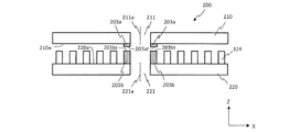
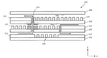
図7Aは、本開示の例示的な実施形態における導波路装置200の一部を模式的に示す斜視図である。この導波路装置200は、第1の導電部材210と、第2の導電部材220とを備えている。第1の導電部材210および第2の導電部材220は、図示されていない周辺部において互いに固定され、間隙を隔てて互いに対向している。図7Aには、互いに直交するX、Y、Z方向を示すXYZ座標が示されている。第1の導電部材210および第2の導電部材220はXY面に沿って拡がっている。この導波路装置200は、図7Aに示される部分の周辺に、図1から図4を参照して説明した導波路装置100と同様のWRG構造を備え得る。そのような構造により、例えば送信波および受信波の一方を、第1の導電部材210の貫通孔211を通して垂直方向(Z軸方向)に伝搬させ、他方を、周辺部のWRG構造を介して伝搬させることができる。第1の導電部材210の貫通孔211を通して垂直方向に伝搬した電磁波は、後述するように他の層におけるWRG構造によってさらに伝搬され得る。
<Embodiment 1: Waveguide Device>
FIG. 7A is a perspective view schematically illustrating a portion of a
図7Bは、図7Aに示す第1の導電部材210の、第2の導電部材220に対向する側の構造を示す斜視図である。第1の導電部材210は、第1の貫通孔211を囲む凸部203aを有する。第1の導電部材210、第1の貫通孔211の内壁、および凸部203aは、いずれも導電性の表面を有している。
FIG. 7B is a perspective view showing the structure of the first
図7Cは、図7Aに示す第2の導電部材220の、第1の導電部材210に対向する側の構造を示す斜視図である。第2の導電部材220は、第2の貫通孔221と、第2の貫通孔221を囲む凸部203bと、凸部203bを囲む複数の導電性ロッド124とを有する。複数の導電性ロッド124は、X方向およびY方向に沿って行列状に配列されている。なお、複数の導電性ロッド124は、行または列に沿って直線上に配列されている必要は無く、単純な規則性を示さずに分散して配置されていても良い。貫通孔221の内壁、凸部203b、および複数の導電性ロッド124は、いずれも導電性の表面を有している。
FIG. 7C is a perspective view showing the structure of the second
図7Dは、導波路装置200の、貫通孔211、221の中心を通るXZ面断面を模式的に示す図である。図7Dおよび以降の断面図では、強調のため、凸部203a、203bのみをハッチングで表している。なお、凸部203a、203b、複数の導電性ロッド124、第1の導電部材210、および第2の導電部材220は、別部材であってもよいし、互いに繋がった1つの部材を構成していてもよい。各構成要素が繋がって1つの部材を構成している場合、構成要素間に明確な境界はないが、図7Dおよび以降の図では、わかり易さのため、構成要素間の境界線を明示している。
FIG. 7D is a view schematically showing an XZ plane cross section passing through the centers of the through
図7Dに示されるように、第1の導電部材210における凸部203aの頂面203atと、第2の導電部材220における凸部203bの頂面203btとは対向しており、両者の間には間隙がある。これらの凸部203a、203bは、その内部において電磁波を伝搬させる導波壁として機能する。このため、本明細書では、凸部203aおよび203bを、併せて「導波壁203」と称することがある。以下、第1の導電部材210における凸部203aを導波壁の「第1部分」と称し、第2の導電部材220における凸部203bを導波壁の「第2部分」と称する。
As shown in FIG. 7D, the
第1の貫通孔211は、軸211aに沿って第1の導電部材210を貫通している。この軸211aを「第1の貫通孔の軸」と称する。第2の貫通孔221は、軸221aに沿って第2の導電部材220を貫通している。この軸221aを「第2の貫通孔の軸」と称する。第2の貫通孔221は、第1の貫通孔211の軸方向に沿って見たときに第1の貫通孔211と重なるように位置している。ここで「重なる」とは、完全に重なる場合のみならず、部分的に重なっている場合を含む。すなわち、第1の貫通孔211を、第2の導電部材220が配置されていない側から軸211aの方向を向いて見たときに、第1の貫通孔211および第2の貫通孔221が、少なくとも部分的に重なる。本実施形態では、第1の導電部材210の導電性表面210aは平面状である。第1の貫通孔211は、導電性表面210aに垂直に第1の導電部材210を貫通している。第2の貫通孔221は、第1の貫通孔211の軸方向に沿って第2の導電部材220を貫通している。すなわち、第1の貫通孔211の軸211aと第2の貫通孔221の軸221aとが一致している。しかし、このような構成に限らず、軸211a、221aが僅かにずれていてもよい。また、軸211a、221aの方向がZ軸に対して若干傾いていてもよい。
The first through
本実施形態では、第1の貫通孔211、導波壁の第1部分203aおよび第2部分203b、ならびに第2の貫通孔221の内壁のXY断面の形状は、Z方向の位置によらず一定である。しかし、このような形態に限定されず、Z方向の位置によってXY断面の形状が変化する貫通孔または導波壁を用いることも可能である。
In the present embodiment, the shape of the XY cross section of the first through
導波壁(第1部分203aおよび第2部分203b)は、他の部材と同様、少なくとも表面が導電性の材料で構成されていれば、必ずしも全体が導電性を有する必要はない。導波壁は、第1の貫通孔211と第2の貫通孔221との間の空間の少なくとも一部を囲んでいればよく、必ずしも当該空間の全てを囲んでいる必要はない。導波壁は、第1の貫通孔211と第2の貫通孔221との間で電磁波を伝搬させる。
The waveguide wall (the
導波路装置200は、自由空間中における中心波長がλo、最短の波長がλmである帯域の電磁波の伝搬に用いられる。波長λoは、例えばミリ波の帯域に属する波長(1mm以上10cm未満)であり、本実施形態では約4mmである。導波壁の第1部分203aの高さと、第2部分203bの高さと、その間の間隙の長さとの合計は、λm/2未満である。ここで、「第1部分203aの高さ」は、第1部分203aの基部(即ち、第1の導電部材210に繋がる部分)から頂面203atまでの距離を意味する。「第2部分203bの高さ」は、第2部分203bの基部(即ち、第2の導電部材220に繋がる部分)から頂面203btまでの距離を意味する。「間隙の長さ」は、第1部分203aと第2部分203bとの間隙のZ方向の長さを意味する。本実施形態のように導波壁が第1部分203aと第2部分203bとに分かれている場合、第1部分203aの高さと第2部分203bの高さとの合計を「導波壁の高さ」と定義する。なお、後述するように、導波壁が第1部分203aおよび第2部分203bの一方のみを有していてもよい。その場合には、その一方の部分の高さが「導波壁の高さ」である。上記の構成に限らず、導波壁の高さはλm/2未満であればよい。これにより、導波壁を通過する際の信号波の反射を抑制し、効率よく信号波を伝搬させることができる。本実施形態では、導波壁の第1部分203aと第2部分203bとの間に間隙があり、接触させる必要がないので製造が容易であるという利点がある。
The
導波壁の頂面203at、203btにおける厚さはλm/2未満である。この条件は、導波壁の頂面203at、203bt上で最低次の共振の発生を防ぐために課される。これにより、導波壁の外側に電磁波が漏洩することを抑制できる。なお、本明細書において「頂面における厚さ」とは、頂面における内周に沿った各点から外周までの最短距離のうち、最も大きい距離を意味する。
The thicknesses of the
本実施形態では、導波壁の第2部分203b高さは、第1部分203aの高さよりも大きく、周囲の導電性ロッド124の高さと同じである。このため、簡易なプロセスで導波壁の第1部分203aと複数の導電性ロッド124とを第2の導電部材220上に形成することができる。しかし、必ずしもこのような形態に限定されない。以下、導波壁の他の構成例を説明する。
In the present embodiment, the height of the
図8Aは、導波壁の他の構成例を示す断面図である。この例では、導波壁の第1部分203aの高さの方が第2部分203bの高さよりも大きい。この例でも第1部分203aと第2部分203bとの間には間隙がある。よって、導波壁の頂面203at、203btにおける厚さはλm/2未満に設定される。なお、電磁波の漏洩をさらに低減するために、導波壁の頂面203at、203btにおける厚さと、導波壁および導電性ロッド124の間の空間の幅の半分と、導電性ロッド124の高さから導波壁の第2部分203bの高さを引いた長さとの合計(図8Aに示す矢印の長さ)は、λm/2未満である。これにより、導波壁の間隙の入り口から導電性ロッド124の先端部に至る領域で最低次の共振が発生することを防ぐことができる。なお、図7Dに示す構成においても同様の条件を満たすように設計される。
FIG. 8A is a cross-sectional view showing another configuration example of the waveguide wall. In this example, the height of the
図8Bは、導波壁のさらに他の構成例を示す断面図である。この例では、分離されていない単一の導波壁203が、第1の導電部材210および第2の導電部材220の両方に接続されている。この例では、導波壁203の高さと、第1の導電部材210の厚さと、第2の導電部材220の厚さとの合計が、λm/2未満に設計される。すなわち、第1の貫通孔211、導波壁203、および第2の貫通孔221によって囲まれる空間のZ方向の長さがλm未満に設計される。これにより、最低次の共振の発生を防ぎ、第1の貫通孔211、導波壁、および第2の貫通孔221を通過する際の反射によるエネルギのロスを低減できる。この例では、導波壁203の厚さに特に制約はない。
FIG. 8B is a cross-sectional view showing yet another configuration example of the waveguide wall. In this example, a single
図8Cは、導波壁のさらに他の構成例を示す断面図である。この例では、導波壁は、第2の導電部材220に繋がる第2部分203bのみを含む。この例における導波壁(第2部分203b)の高さは導電性ロッド124の高さと同じであるが、異なっていてもよい。導波壁(第2部分203b)と第1の導電部材210との間には間隙がある。間隙から電磁波のエネルギが漏洩することを抑制するために、導波壁(第2部分203b)の頂面における厚さは、λm/2未満に設定される。
FIG. 8C is a cross-sectional view showing yet another configuration example of the waveguide wall. In this example, the waveguide wall includes only the
図8Dは、導波壁のさらに他の構成例を示す断面図である。この例では、導波壁は、第1の導電部材210に繋がる第1部分203aのみを含む。導波壁(第1部分203a)と第2の導電部材220との間には間隙がある。間隙から電磁波のエネルギが漏洩することを防ぐために、導波壁(第1部分203a)の頂面における厚さは、λm/2未満に設定される。
FIG. 8D is a cross-sectional view showing yet another configuration example of the waveguide wall. In this example, the waveguide wall includes only the
図8Eは、導波壁のさらに他の構成例を示す断面図である。この例では、導波壁203は、第1の導電部材210にも第2の導電部材220にも接続されていない単一の部分のみを含んでいる。この導波壁203は、図示されていない部材によって第1の導電部材210および第2の導電部材220に固定されている。導波壁203と第1の導電部材210との間、および導波壁203と第2の導電部材220との間の両方に間隙が存在する。間隙から電磁波のエネルギが漏洩することを防ぐために、導波壁203の頂面における厚さは、λm/2未満に設定される。なお、この例では、導波壁203の頂面は、第1の導電部材210の導電性表面210aに対向する面、および第2の導電部材220の導電性表面220aに対向する面の両方を指す。
FIG. 8E is a cross-sectional view showing yet another configuration example of the waveguide wall. In this example, the
以上のいずれの構成においても、複数の導電性ロッド124のうち、導波壁に隣接する(即ち、最も近い)導電性ロッド124と導波壁の外周との距離はλm/2未満に設定される。第1の導電部材210および第2の導電部材220の少なくとも一方、ならびに導波壁は、繋がった一つの部材を構成していてもよい。言い換えれば、第1の導電部材210および第2の導電部材220の少なくとも一方、ならびに導波壁は、単一構造体の一部であり得る。導波壁が第1部分203aと第2部分203bとに分かれている構成においては、第1の導電部材210と第1部分203aとが単一構造体の一部であり、第2の導電部材220と第2部分203bとが他の単一構造体の一部であってもよい。このような単一構造体は、例えば同一の材料で構成され、切削、絞り、または成型等の工程を経て製造された単一の部材であり得る。単一構造体は、例えば3Dプリンタを用いて製造することも可能である。そのような、構成要素間の境界が明確ではない構成も、本開示の実施形態に含まれる。
In any of the above configurations, among the plurality of
次に、導波壁および貫通孔211、221の断面形状の例を説明する。
Next, an example of the cross-sectional shape of the waveguide wall and the through
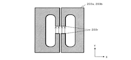
図9Aは、導波壁の第2部分203bのXY断面の形状の例を模式的に示す図である。第1部分203aおよび貫通孔211、221も同様の断面形状を有する。この例では、導波壁の第1部分203a、導波壁の第2部分203b、および貫通孔211、221の各々の内壁面は、内側に向かって突出する2つの突出部203rを有する。この開口の断面の形状は、アルファベットの「H」に類似しており、X方向に延びる1つの横部分203Tと、横部分の両端からY方向に延びる一対の縦部分203Lとを有する。この例では、縦部分203Lは横部分203Tに対して垂直に延びているが、必ずしも垂直に延びている必要はない。より一般的には、縦部分203Lは横部分203Tの延びる方向に対して交差する方向に延びる。以下、このような形状をH型形状またはダブル突出部形状と称することがある。図9AではH型形状の横部分203TがX軸方向に平行であるが、横部分203TがX軸方向に対して傾斜していてもよい。開口の断面形状は、H型形状の中心点(横部分203Tの中心点)から端部(縦部分203Lのいずれかの端部)までの、横部分203Tおよび縦部分203Lに沿った長さの2倍がλo/2以上になるように設計され得る。これにより、導波壁が中空導波管として機能し、主に一対の突出部203r(横部分203T)に沿って電磁波を伝搬させることができる。H型形状にすることにより、開口の横部分203Tに沿った方向のサイズを小さくすることができる。横部分203Tの中央における導波壁の厚さ(即ち、突出部203rがある部分における導波壁の第2部分203bのY方向における厚さ)は、λo/4あるいはλo/4の0.8倍以上1.2倍以下とすることが好ましい。この寸法範囲とすることにより、貫通孔からの電磁波の漏洩をより確実に抑制できる。
FIG. 9A is a view schematically showing an example of the shape of the XY cross section of the
図9Bは、導波壁の第2部分203bのXY断面の形状の他の例を模式的に示す図である。第1部分203aおよび貫通孔211、221も同様の断面形状を有する。この例では、第1の貫通孔、第2の貫通孔、および導波壁の、導電性表面210aに沿った断面形状は、一方向に長い形状(長尺形状)であり、横部分203Tのみを有している。このような形状は、矩形(方形)の形状に限らず、楕円形状のように両端が丸い形状でもよい。このような形状は、アルファベットの「I」に類似しているため、I型形状と称することがある。開口の長さ方向(X方向)の寸法は、λo/2より大きな寸法に設定される。図9Aの構造に比して、長さ方向(図9Bの例ではX方向)のサイズが大きくなるが、孔の形状は単純化される。貫通孔の縁から導波壁の第2部分203bの長辺の縁までのY方向における寸法は、λo/4あるいはλo/4の0.8倍以上1.2倍以下とすることが好ましい。この寸法範囲とする事により、貫通孔から電磁波の漏洩をより確実に抑制できる。
FIG. 9B is a view schematically showing another example of the shape of the XY cross section of the
図9Cは、導波壁の第2部分203bのXY断面の形状のさらに他の例を模式的に示す図である。第1部分203aおよび貫通孔211、221も同様の断面形状を有する。この例では、導波壁の第1部分203a、導波壁の第2部分203b、および貫通孔211、221の各々の内壁面は、内側に向かって突出する1つの突出部203rを有する。このような形状を、シングル突出部形状と称することがある。このように、導波壁の内壁面が、内側に向かって突出する少なくとも1つの突出部203rを有することにより、突出部203rに沿って電磁波を伝搬させることができる。シングル突出部形状においても、導波壁の外壁面には、他に一つ以上の突出部を有していてもよい。図9Cの例においては、突出部203rを有する側とは反対の側において、導波壁の外壁面は外側に向かって突出する1つの外側突出部203r2を有する。この例において、外側突出部203r2のX方向における幅は、突出部203rのX方向における幅よりも広い。但し、外側突出部203r2が、突出部203rの幅と略同一の幅を持つ構造も採用可能である。この例における開口は、X方向に延びる1つの横部分203Tと、横部分203Tの両端から同じ方向である+Y方向に延びる一対の縦部分203Lとを有する。この例では、一対の縦部分203Lにおける一方の端部(図9Cにおける右上の端部)から他方の端部(図9Cにおける左上の端部)までの、一対の縦部分203Lおよび横部分203Tに沿った長さは、λo/2より大きな寸法に設計される。横部分203Tの中央における導波壁の厚さ(即ち、突出部203rがある部分における導波壁の第2部分203bのY方向における厚さ)は、λo/4あるいはλo/4の0.8倍以上1.2倍以下とすることが好ましい。貫通孔の縁から導波壁の第2部分203bの長辺の縁までのY方向における寸法についても、λo/4あるいはλo/4の0.8倍以上1.2倍以下とすることが好ましい。この寸法範囲とする事により、貫通孔から電磁波の漏洩をより確実に抑制できる。
FIG. 9C is a view schematically showing still another example of the shape of the XY cross section of the
図9Dは、導波壁の第2部分203bのXY断面の形状のさらに他の例を模式的に示す図である。第1部分203aおよび貫通孔211、221も同様の断面形状を有する。この例における断面形状は、X方向に延びる1つの横部分203Tと、横部分203Tの両端から互いに異なる方向(+Z方向と−Z方向)に延びる一対の縦部分203Lとを有する。このような形状は、アルファベットの「Z」または反転した「Z」の形状に類似するため、「Z型形状」と称することがある。Z型形状の中心点(横部分203Tの中心点)から端部(縦部分203Lのいずれかの端部)までの、横部分203Tおよび縦部分203Lに沿った長さの2倍がλo/2以上になるように開口の断面形状は設計され得る。
FIG. 9D is a view schematically showing still another example of the shape of the XY cross section of the
図10は、開口の形状がH型形状である場合に形成される電界の強度分布の一例を模式的に示す図である。導波壁を電磁波が伝搬しているとき、導波壁内には、図10に例示されるような電界が形成され得る。図10において、電界の向きが矢印で表され、電界の強さが矢印の長さで表されている。電界は、一対の突出部の間において相対的に強く、突出部の周辺部において相対的に弱い。電磁波は、このような電界分布で、主に突出部に沿って伝搬する。 FIG. 10 is a view schematically showing an example of an intensity distribution of an electric field formed when the shape of the opening is an H-shape. When an electromagnetic wave propagates through the waveguide wall, an electric field as illustrated in FIG. 10 can be formed in the waveguide wall. In FIG. 10, the direction of the electric field is represented by an arrow, and the strength of the electric field is represented by the length of the arrow. The electric field is relatively strong between the pair of protrusions and relatively weak at the periphery of the protrusions. An electromagnetic wave propagates mainly along the protrusion in such an electric field distribution.
以上の例では、導波壁(第1部分203aおよび第2部分203b)は、第1の貫通孔211と第2の貫通孔221との間の(間隙を除く)空間の周囲を完全に囲んでいるが、このような形態に限定されない。
In the above example, the waveguide wall (the
図11は、導波壁の他の構成例を示す図である。この例では、導波壁は、2つの部分に分割されている。2つの部分の一方のXY断面の形状は、H型形状の半分(横部分の半分と1つの縦部分)の形状である。このような導波壁を用いても、図11に示すように、対向する突出部203r間に強い電界が形成されるため、前述の例と同様に電磁波を伝搬させることができる。
FIG. 11 is a view showing another configuration example of the waveguide wall. In this example, the waveguiding wall is divided into two parts. The shape of the XY cross section of one of the two parts is the shape of a half of the H-shape (half of the horizontal part and one vertical part). Even when such a waveguide wall is used, as shown in FIG. 11, a strong electric field is formed between the facing
次に、本実施形態における導波路装置200と、前述のリッジ導波路(WRG)とを組み合わせた例を説明する。本実施形態における導波路装置200は、前述のWRGの構造と組み合わせることで、目的に応じて様々な給電路を構成できる。
Next, an example in which the
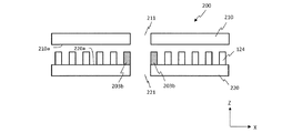
図12Aは、第2の導電部材220の下にWRGの構造を有する第3の導電部材230を有する例を示す断面図である。第3の導電部材230は、Y方向に延びる導波部材122と、導波部材122の両側に位置する複数の導電性ロッド124とを有している。ここで、第3の導電部材230の上側の面に配置される複数の導電性ロッド124を、第2の複数の導電性ロッドと呼ぶことができる。導波部材122の導波面および導電性ロッド124の先端部は、第2の導電部材220の導電性表面220bに対向している。
FIG. 12A is a cross-sectional view showing an example having a third
図12Bは、第2の導電部材220の上下に導電性ロッド124を有する例を示す断面図である。第2の導電部材220の下側の面には、複数の導電性ロッド124および導波部材122が配置されている。第2の導電部材220の上側の面(導電性表面220a)に配置される複数の導電性ロッド124を第1の複数の導電性ロッド124と呼び、第2の導電部材220の下側の面(導電性表面220b)に配置される複数の導電性ロッド124を第2の複数の導電性ロッド124と呼ぶことができる。第3の導電部材230は、第2の導電部材220の下方に配置される板状の部材であり、導電性表面220bに対向する導電性表面230aを有する。この例において、第2の導電部材220の下側の導波部材122はY方向に延び、その両側に複数の導電性ロッド124が並ぶ。この導波部材122の導波面および導電性ロッド124の先端部は、第3の導電部材230の導電性表面230aに対向している。また、第2の貫通孔221は、導波部材122の導波面の端部または他の部分に開口する。
FIG. 12B is a cross-sectional view showing an example in which
図13は、図12Aにおける第3の導電部材230をZ軸の正方向から見た上面図である。導波部材122の両側には、複数の導電性ロッド124の配列によって構成された人工磁気導体が形成されている。導波部材122の一端には、複数の導電性ロッド124がY方向に並び、チョーク構造129が形成されている。チョーク構造129は、先端が開放された導波部材(リッジ)122の端部と、そのリッジ122の端部の延長方向に並ぶ、高さが約λo/4の複数の導電性ロッドを含む。このチョーク構造に含まれるリッジの長さは、リッジ導波路における電磁波の波長λgとするとき、λg/4である。このチョーク構造129により、導波部材122の一端から電磁波が漏洩することを抑制でき、効率よく電磁波を伝送することができる。
FIG. 13 is a top view of the third
第3の導電部材230は、導波部材122の他端に近接するポート(開口部)145を有している。ポート145を介して不図示の送信回路(電子回路)から導波部材122上の導波路に電磁波が供給され得る。逆に、導波部材122上の導波路を伝搬した電磁波がポート145を介してさらに下層の導波路に伝送され得る。なお、第3の導電部材230における導波部材122の導波面は、そのいずれかの部位において第2の貫通孔221に対向していればよい。
The third
図14は、第1の導電部材210の上にWRGの構造が設けられた例を示す断面図である。この例では、第1の導電部材210が、導電性表面210aの反対側の表面に、導波部材122と、複数の導電性ロッド124とを備えている。導波部材122の一端は、第1の貫通孔211の側壁に繋がっている。第1の導電部材210に対向して、他の導電部材240が配置されている。導電部材240の導電性表面240aと、導波部材122の導波面および導電性ロッド124の先端部とは対向している。導電性表面240aと導波面との間に導波路が形成される。
FIG. 14 is a cross-sectional view showing an example in which the structure of the WRG is provided on the first
図15は、図14における第1の導電部材210をZ軸の正方向側から見た上面図である。第1の導電部材210における第1の貫通孔211の位置からY軸の負方向にストライプ状(「ストリップ形状」と称することもある。)の導波部材122が延びている。導波部材122の周囲には、複数の導電性ロッド124が二次元的に配列されている。これらの導電性ロッド124によって人工磁気導体が形成されている。導波壁および第1の貫通孔211を通過した電磁波は、導波部材122上の導波面に沿って伝搬することができる。導波部材122上と導電性表面240aとの間の導波路は、不図示の少なくとも1つのアンテナ素子(例えばスロット)に接続されたり、さらに上部の層の導波路に接続されたりしてもよい。なお本明細書において「ストライプ形状」とは、縞(stripes)の形状を意味するのではなく、単一のストライプ(a stripe)の形状を意味する。一方向に直線的に延びる形状だけでなく、途中で曲がったり、分岐したりする形状も「ストライプ形状」に含まれる。なお、導波面122a上に高さまたは幅の変化する部分が設けられている場合も、導波面122aの法線方向から見て一方向に沿って延びる部分を含む形状であれば、「ストライプ形状」に該当する。
FIG. 15 is a top view of the first
図16は、図12Aおよび図14の構成を組み合わせた構成例を示す断面図である。このような構成によれば、第3の導電部材230における導波部材122上の導波路と、第1の導電部材210における導波部材122上の導波路とが、第2の貫通孔211、導波壁(第1部分203aおよび第2部分203b)、および第2の貫通孔221を介して接続される。このため、上下2つの導波路の間で、電磁波を伝搬させることができる。また、第3の導電部材230には、貫通孔221に対してY方向における正の側に、Y方向における長さがλg/4のリッジを含むチョーク構造229が設けられている。チョーク構造229によって導波部材122のY方向正の側の端部から電磁波が漏洩することを抑制でき、効率よく電磁波を伝送することができる。
FIG. 16 is a cross-sectional view showing a configuration example in which the configurations of FIG. 12A and FIG. 14 are combined. According to such a configuration, the waveguide on the
図17は、2つの導波層を越えて電磁波を伝搬させることのできる導波路装置200の構成例を模式的に示す断面図である。この例における導波路装置200は、第1の導電部材210、第2の導電部材220、第3の導電部材230、および他の導電部材240、250を備えている。第3の導電部材230は、各々が第2の導電部材220の導電性表面220bに対向する先端部を持つ第2の複数の導電性ロッド124と、第2の貫通孔221の軸方向に沿って見たときに第2の貫通孔221と重なる第3の貫通孔231と、第2の貫通孔221と第3の貫通孔231との間の空間の少なくとも一部を囲む導電性の他の導波壁233(第1部分233aおよび第2部分233b)とを有している。導波壁233は、第3の導電部材230における第2の複数の導電性ロッド124に囲まれ、第2の貫通孔221と第3の貫通孔231との間で電磁波を伝搬させる。他の導波壁233についても、高さ(第1部分233aおよび第2部分233bの高さの合計)はλm/2未満である。第2の複数の導電性ロッド124の内、導波壁233に隣接する導電性ロッド124と、導波壁233の外周との距離はλm/2未満である。図17に示す例では、導波壁233は、導電部材220の裏面側(導電性表面220bの側)に接続された第1部分233aと、導電部材230に接続された第2部分233bとに分かれているが、1つの部分から構成されていてもよい。導波壁233は、導電部材220、230の少なくとも一方に繋がっていてもよいし、図8Eに示す例のように、いずれの導電部材にも繋がっていなくてもよい。導電部材220、230の少なくとも一方と、導波壁233の少なくとも一部は、単一構造体の一部であってもよい。導波壁233についても、前述の導波壁203と同様、頂面における厚さはλm/2未満に設定される。
FIG. 17 is a cross-sectional view schematically showing a configuration example of a
この例では、導電部材210と導電部材220との間の層、および導電部材220と導電部材230との間の層の2層を越えて電磁波を伝搬させることができる。このため、スキップされる当該2層の空間に、他の導波路またはカメラ等の構造物を配置することができる。なお、図17における導電部材250の代わりに、さらに他の導波壁を有する部材を配置してもよい。そのような構成によれば、3つ以上の層を飛び越えて電磁波を伝搬させることができる。
In this example, electromagnetic waves can be propagated across two layers of the layer between the
図18は、導波壁203が配置された層に他の導波路が形成された構成例を模式的に示す断面図である。この導波路装置200は、図16に示す構成に加えて、第2の導電部材220上および第3の導電部材230上に他のリッジ導波路をさらに有している。この例では、第3の導電部材230は、複数の導電性ロッド124を隔てて2つのストライプ状の導波部材122を有する。
FIG. 18 is a cross-sectional view schematically showing a configuration example in which another waveguide is formed in the layer in which the
図19は、図18に示す導波路装置200における第2の導電部材220をZ軸の正方向から見た上面図である。この例における第2の導電部材220は、複数の導電性ロッド124の間に、導電性表面210aに対向する導電性の導波面を有する導波部材122をさらに有している。導波部材122は、導波壁203から複数の導電性ロッド124を隔てて配置されている。導波部材122の導波面と第1の導電部材の導電性表面210aとの間に導波路が形成される。この導波路は、ポート145を介して、第3の導電部材230における導波部材122上の導波路に接続される。
FIG. 19 is a top view of the second
第2の導電部材220における導波部材122上の導波路を伝搬する電磁波は、導波壁203内を伝搬する電磁波とは異なる信号を伝送することができる。例えば、前者の電磁波は受信用のアンテナ素子から伝送された受信波であり、後者の電磁波は送信用のアンテナ素子に伝送される送信波であり得る。このような構成により、限られたスペースに必要な導波路構造が設けられた小型のアンテナ装置を実現できる。
The electromagnetic wave propagating in the waveguide on the
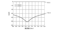
次に、図20Aおよび図20Bを参照しながら、本実施形態における導波壁を通過する電磁波の透過・反射特性を説明する。図20Aおよび図20Bは、各部材の寸法等を適切な値に設定してシミュレーションを行った結果を示している。 Next, transmission and reflection characteristics of an electromagnetic wave passing through the waveguide wall in the present embodiment will be described with reference to FIGS. 20A and 20B. FIG. 20A and FIG. 20B show the results of simulation performed by setting the dimensions and the like of the respective members to appropriate values.
図20Aは、図7Aから7Dに示される導波路装置200の導波壁における散乱パラメータ(Sパラメータ)の周波数依存性を示すグラフである。Sパラメータは、散乱行列(S行列)の行列要素であり、回路を伝搬する信号波の透過・反射特性を表す。図20AにおけるS(1,1)は、入力波の強度に対する反射波の強度の割合を示し、S(2,1)は、入力波の強度に対する透過波の強度の割合を示している。
FIG. 20A is a graph showing the frequency dependence of the scattering parameter (S-parameter) in the waveguide wall of the
図20Aからわかるように、S(1,1)が−50dBから−30dB(10-5倍から10-3倍)程度の非常に小さい値になるのに対して、S(2,1)は、ほぼ0dB(1倍)である。このことは、電磁波が本実施形態における導波壁を通過する際に、反射が殆ど生じない(即ち、ロスが小さい)ことを意味している。 As can be seen from FIG. 20A, while S (1,1) becomes a very small value of about −50 dB to −30 dB (10 −5 to 10 −3 times), S (2, 1) is , Approximately 0 dB (one time). This means that when the electromagnetic wave passes through the waveguide wall in the present embodiment, almost no reflection occurs (that is, the loss is small).
図20Bは、導波壁の近傍に隣接ポートが配置されている場合におけるSパラメータの周波数依存性を示すグラフである。この場合、導波壁から隣接ポートへのエネルギの漏洩が生じ得ることから、S行列は4行4列になる。この場合、S(1,1)は、入力波の強度に対する反射波の強度の割合を示し、S(2,1)は、入力波の強度に対する透過波の強度の割合を示し、S(3,1)およびS(4,1)は、入力波の強度に対する隣接ポートへの漏洩波の強度の割合を示す。 FIG. 20B is a graph showing frequency dependence of S parameters in the case where adjacent ports are arranged in the vicinity of the waveguide wall. In this case, since the leakage of energy from the waveguide wall to the adjacent port may occur, the S matrix has 4 rows and 4 columns. In this case, S (1,1) indicates the ratio of the intensity of the reflected wave to the intensity of the input wave, S (2,1) indicates the ratio of the intensity of the transmitted wave to the intensity of the input wave, S (3 (3) , 1) and S (4, 1) indicate the ratio of the strength of the leaked wave to the adjacent port to the strength of the input wave.
図20Bからわかるように、S(1,1)、S(3,1)、S(4,1)が−37dBから−25dB程度の非常に小さい値になるのに対して、S(2,1)は、ほぼ0dB(1倍)である。このことは、電磁波が導波壁を通過する際に、反射および隣接ポートへの漏洩が殆ど生じない(即ち、ロスが小さい)ことを意味している。 As can be seen from FIG. 20B, S (1, 2), S (3, 1), S (4, 1) have extremely small values of about −37 dB to about −25 dB, while S (2, 1) is approximately 0 dB (1 ×). This means that when the electromagnetic wave passes through the waveguide wall, reflection and leakage to the adjacent port hardly occur (that is, the loss is small).
このように、本実施形態によれば、導波壁を介して電磁波を高い効率で伝搬させることができる。 Thus, according to the present embodiment, an electromagnetic wave can be propagated with high efficiency through the waveguide wall.
<実施形態2:アンテナ装置>
次に、本開示の導波路装置を備えたアンテナ装置の例示的な実施形態を説明する。本実施形態のアンテナ装置は、実施形態1における導波路装置と、当該導波路装置における導波壁内の導波路に接続された少なくとも1つのアンテナ素子とを備える。「導波壁内の導波路に接続される」とは、導波壁内の導波路に直接的に、または前述したWRG等の他の導波路を介して間接的に接続されることを意味する。少なくとも1つのアンテナ素子は、導波壁内の導波路を伝搬した電磁波を空間に向けて放射する機能、および空間を伝搬してきた電磁波を導波壁内の導波路に導入する機能の少なくとも一方を有する。すなわち、本実施形態におけるアンテナ装置は、信号の送信および受信の少なくとも一方に用いられる。
Embodiment 2: Antenna Device
An exemplary embodiment of an antenna device comprising a waveguide device of the present disclosure will now be described. The antenna device of the present embodiment includes the waveguide device in the first embodiment and at least one antenna element connected to the waveguide in the waveguide wall of the waveguide device. “Connected to a waveguide in a waveguide wall” means connected directly to the waveguide in the waveguide wall or indirectly via another waveguide such as the above-mentioned WRG. Do. At least one of the antenna elements has a function of radiating an electromagnetic wave propagating in the waveguide in the waveguide wall toward the space, and a function of introducing an electromagnetic wave propagating in the space into the waveguide in the waveguide wall Have. That is, the antenna device in the present embodiment is used for at least one of transmission and reception of a signal.
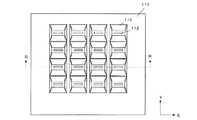
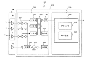
図21Aは、複数のスロット(開口部)が配列されたアンテナ装置(アレーアンテナ)の例を示す図である。図21Aはアンテナ装置を+Z方向から見た上面図である。図21Bは、図21AのB−B線断面図である。図示されるアンテナ装置においては、アンテナ素子(放射素子)として機能する複数のスロット112に直接的に結合する複数の導波部材122Uを含む第1の導波層10aと、複数の導電性ロッド124Mおよび不図示の導波壁を含む第2の導波層10bと、第1の導波層10aの導波部材122Uに導波壁を介して結合する他の導波部材122Lを含む第3の導波層10cとが積層されている。第1の導波層10aにおける複数の導波部材122U、および複数の導電性ロッド124Uは、第1の導電部材210上に配置されている。第2の導波層10bにおける複数の導電性ロッド124Mおよび不図示の導波壁は、第2の導電部材220上に配置されている。第3の導波層10cにおける導波部材122Lおよび複数の導電性ロッド124Lは、第3の導電部材230上に配置されている。
FIG. 21A is a diagram showing an example of an antenna apparatus (array antenna) in which a plurality of slots (openings) are arranged. FIG. 21A is a top view of the antenna device as viewed from the + Z direction. 21B is a cross-sectional view taken along line B-B of FIG. 21A. In the illustrated antenna device, a
このアンテナ装置は、第1の導波層10aにおける導波部材122Uおよび導電性ロッド124Uを覆う導電部材110をさらに備えている。導電部材110は、4行4列に配列された16個のスロット(開口部)112を有する。導電部材110には、各スロット112を囲む側壁114が設けられている。側壁114は、スロット112の指向性を調整するホーンを形成している。この例におけるスロット112の個数および配列は、例示的なものに過ぎない。スロット112の向きおよび形状も、図示される例に限定されない。例えば、H型形状のスロットを用いてもよい。ホーンの側壁114の傾斜の有無および角度、ならびにホーンの形状も、図示されている例に限定されない。
The antenna device further includes a
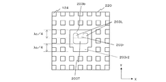
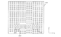
図22Aは、第1の導電部材210における導波部材122Uおよび導電性ロッド124Uの平面レイアウトを示す図である。図22Bは、第2の導電部材220における導電性ロッド124M、導波壁203および貫通孔221の平面レイアウトを示す図である。図22Cは、第3の導電部材230における導波部材122Lおよび導電性ロッド124Lの平面レイアウトを示す図である。これらの図から明らかなように、第1の導電部材210における導波部材122Uは直線状(ストライプ状)に延びており、分岐部も屈曲部も有していない。一方、第3の導電部材230における導波部材122Lは延びる方向が2つに分かれる分岐部および延びる方向が変化する屈曲部の両方を有している。第1の導電部材210における貫通孔211と第2の導電部材220における貫通孔221との間には、図22Bに示すように、実施形態1において説明した導波壁203が配置されている。
FIG. 22A is a diagram showing a planar layout of the
図22Bに示す例では、第2の導電部材220上に4つの導波壁203が存在する。これらの導波壁203と、それらに隣接するロッド124Mとの配置関係は、導波壁203によって異なっている。内側に突出部を有する導波壁203の該突出部を含む厚さは、図9Aに示すように、約λo/4に設定され得る。そのような導波壁203を配置する場合、隣接する導電性ロッド124Mとの間隔を調節する必要が生じる。図22Bは、そのバリエーションを示している。図において左右両端の導波壁221については、Y方向に隣接する6個のロッド124MのみがY方向に僅かにずれ、導波壁203とこれらのロッド124Mとが接触しないように調整されている。左から2番目の導波壁221については、Y方向に隣接する6個のロッド124Mが除去されている。左から3番目の導波壁221については、X座標が重なる3列のロッド124MのY方向の配置の位相がずれている。これらの何れの例でも機能する。また、導波壁203の外周面と、隣接するロッド124Mの外周面との間隔はλm/2未満である。
In the example shown in FIG. 22B, four
第1の導電部材210における導波部材122Uは、貫通孔211、導波壁、および貫通孔221を通じて第3の導電部材230における導波部材122Lに結合する。言い換えると、第3の導電部材230上の導波部材122Lに沿って伝搬してきた電磁波は、貫通孔221、導波壁、および貫通孔211を通って第1の導電部材210上の導波部材122Uに達し、導波部材122Uに沿って伝搬することができる。このとき、各スロット112は、導波路を伝搬してきた電磁波を空間に向けて放射するアンテナ素子として機能する。反対に、空間を伝搬してきた電磁波がスロット112に入射すると、その電磁波はスロット112の直下に位置する導波部材122Uに結合し、導波部材122Uに沿って伝搬する。導波部材122Uを伝搬してきた電磁波は、貫通孔211、導波壁、および貫通孔221を通って第3の導電部材230上の導波部材122Lに達し、導波部材122Lに沿って伝搬することも可能である。導波部材122Lは、第3の導電部材230が有するポート145Lを介して、外部にある導波路装置または高周波回路(電子回路)に結合され得る。図22Cには、一例として、ポート145Lに接続された電子回路290が示されている。電子回路290は、特定の位置に限定されず、任意の位置に配置されていてよい。電子回路290は、例えば、第3の導電部材210の背面側(図21Bにおける下側)の回路基板に配置され得る。このような電子回路は、マイクロ波集積回路であり、例えば、ミリ波を生成または受信するMMIC(Monolithic Microwave Integrated Circuit)であり得る。
The
図21Aに示される導電部材110を「放射層」と呼ぶことができる。また、図22Aに示される第1の導電部材210上の導波部材122Uおよび導電性ロッド124Uの全体を含む層を「励振層」と呼び、図22Bに示される第2の導電部材220上の導電性ロッド124Mおよび導波壁の全体を含む層を「中間層」と呼び、図22Cに示される第3の導電部材230上の導波部材122Lおよび導電性ロッド124Lの全体を含む層を「分配層」と呼んでも良い。また、「励振層」、「中間層」、および「分配層」をまとめて「給電層」と呼んでも良い。「放射層」、「励振層」、「中間層」、および「分配層」は、それぞれ、一枚の金属プレートを加工することによって量産され得る。放射層、励振層、分配層、および分配層の背面側に設けられる電子回路は、モジュール化された1つの製品として製造され得る。
The
この例におけるアレーアンテナでは、図21Bからわかるように、プレート状の放射層、励振層および分配層が積層されているため、全体としてフラットかつ低姿勢(low profile)のフラットパネルアンテナが実現している。例えば、図21Bに示す断面構成を持つ積層構造体の高さ(厚さ)を20mm以下にすることができる。 In the array antenna in this example, as can be seen from FIG. 21B, since the plate-like radiation layer, the excitation layer and the distribution layer are laminated, a flat and low profile flat panel antenna is realized as a whole. There is. For example, the height (thickness) of the laminated structure having the cross-sectional configuration shown in FIG. 21B can be 20 mm or less.
図22Cに示される導波部材122Lによれば、第3の導電部材230のポート145Lから第1の導電部材210の各貫通孔211(図22A参照)までの、導波部材122Lに沿って測った距離がすべて等しい。このため、第3の導電部材230のポート145Lから導波部材122Lに入力された信号波は、第1の導電部材210の4つの貫通孔211のそれぞれに同じ位相で到達する。その結果、第1の導電部材210上に配置された4個の導波部材122Uは、同位相で励振され得る。
According to the
なお、アンテナ素子として機能する全てのスロット112が同位相で電磁波を放射する必要はない。励振層および分配層における導波部材122のネットワークパターンは任意であり、各導波部材122が互いに異なる信号を独立して伝搬するように構成されていても良い。
Note that it is not necessary for all the
本実施形態における第1の導電部材210上の導波部材122Uは分岐部も屈曲部も有していないが、励振層として機能する部分が分岐部および屈曲部の少なくとも一方を有する導波部材を備えていても良い。前述したように、導波路装置内の全ての導電性ロッドが同様の形状を有している必要はない。
Although the
本実施形態によれば、第1の導電部材210における貫通孔211と第2の導電部材220における貫通孔221との間で、導電性の導波壁203を介して直接的に電磁波を伝搬させることができる。第2の導電部材220上で不要な伝搬が生じないため、第2の導電部材220上に他の導波路、回路基板、またはカメラ等の構造物を配置することができる。このため、装置の設計の自由度を向上させることができる。なお、本実施形態では第1の導電部材210と第2の導電部材220との間に導波壁を配置しているが、導波壁は他の位置に配置してもよい。また、必要に応じて複数の導波壁を配置してもよい。
According to the present embodiment, the electromagnetic wave is directly propagated through the
本実施形態における導波路装置およびアンテナ装置は、例えば車両、船舶、航空機、ロボット等の移動体に搭載されるレーダまたはレーダシステムに好適に用いられ得る。レーダは、本開示の実施形態におけるアンテナ装置と、当該アンテナ装置に接続されたマイクロ波集積回路とを備える。レーダシステムは、当該レーダと、当該レーダのマイクロ波集積回路に接続された信号処理回路とを備える。本実施形態のアンテナ装置は、小型化が可能な多層のWRG構造を備えているため、従来の中空導波管を用いた構成と比較して、アンテナ素子が配列される面の面積を著しく小さくすることができる。このため、当該アンテナ装置を搭載したレーダシステムを、例えば車両のリアビューミラーの鏡面の反対側の面のような狭小な場所、またはUAV(Unmanned Aerial Vehicle、所謂ドローン)のような小型の移動体にも容易に搭載することができる。なお、レーダシステムは、車両に搭載される形態の例に限定されず、例えば道路または建物に固定されて使用され得る。 The waveguide device and the antenna device in the present embodiment can be suitably used, for example, in a radar or a radar system mounted on a mobile object such as a vehicle, a ship, an aircraft, a robot or the like. The radar includes the antenna device in the embodiment of the present disclosure and a microwave integrated circuit connected to the antenna device. The radar system includes the radar and a signal processing circuit connected to a microwave integrated circuit of the radar. The antenna device of the present embodiment is provided with a multilayer WRG structure that can be miniaturized, so the area of the surface on which the antenna elements are arranged is significantly reduced compared to the configuration using a conventional hollow waveguide. can do. For this reason, the radar system mounted with the antenna device is, for example, in a narrow place such as a surface opposite to the mirror surface of a rear view mirror of a vehicle or a small mobile such as a UAV (Unmanned Aerial Vehicle). Can be easily mounted. In addition, a radar system is not limited to the example of the form mounted in a vehicle, For example, it can be fixed and used for a road or a building.
本開示の実施形態におけるスロットアレーアンテナは、無線通信システムにも利用できる。そのような無線通信システムは、上述したいずれかの実施形態におけるスロットアレーアンテナと、通信回路(送信回路または受信回路)とを備える。無線通信システムへの応用例の詳細については、後述する。 The slot array antenna in the embodiment of the present disclosure can also be used in a wireless communication system. Such a wireless communication system includes the slot array antenna in any of the above-described embodiments and a communication circuit (transmission circuit or reception circuit). Details of application examples to the wireless communication system will be described later.
本開示の実施形態におけるスロットアレーアンテナは、さらに、屋内測位システム(IPS:Indoor Positioning System)におけるアンテナとしても利用することができる。屋内測位システムでは、建物内にいる人、または無人搬送車(AGV:Automated Guided Vehicle)などの移動体の位置を特定することができる。スロットアレーアンテナはまた、店舗または施設に来場した人が有する情報端末(スマートフォン等)に情報を提供するシステムにおいて用いられる電波発信機(ビーコン)に用いることもできる。そのようなシステムでは、ビーコンは、例えば数秒に1回、IDなどの情報を重畳した電磁波を発する。その電磁波を情報端末が受信すると、情報端末は、通信回線を介して遠隔地のサーバコンピュータに、受け取った情報を送信する。サーバコンピュータは、情報端末から得た情報から、その情報端末の位置を特定し、その位置に応じた情報(例えば、商品案内またはクーポン)を、当該情報端末に提供する。 The slot array antenna in the embodiment of the present disclosure can also be used as an antenna in an indoor positioning system (IPS). In the indoor positioning system, it is possible to identify the position of a person in a building or a mobile object such as an automated guided vehicle (AGV). The slot array antenna can also be used for a radio wave transmitter (beacon) used in a system for providing information to an information terminal (such as a smartphone) possessed by a person who has visited a store or facility. In such a system, a beacon emits an electromagnetic wave superimposed with information such as an ID, for example, once every several seconds. When the information terminal receives the electromagnetic wave, the information terminal transmits the received information to the remote server computer via the communication line. The server computer specifies the position of the information terminal from the information obtained from the information terminal, and provides the information terminal (for example, a product guide or a coupon) according to the position to the information terminal.
なお、本明細書では、本発明者の一人である桐野による論文(非特許文献1)、および同時期に関連する内容の研究を発表したKildalらの論文の記載を尊重して、「人工磁気導体」という用語を用いて本開示の技術を記載している。しかし、本発明者らの検討の結果、本開示に係る発明には、従来の定義における「人工磁気導体」を、必ずしも必須としないことが明らかになってきている。即ち、人工磁気導体には、周期構造が必須であると考えられてきたが、本開示に係る発明を実施するためには、必ずしも周期構造は必須ではない。 In addition, in this specification, in view of the description of the article by Sugano, who is one of the present inventors (Non-Patent Document 1), and the article of Kildal et al. Who published the study of the contents related to the same period, The term "conductor" is used to describe the technology of the present disclosure. However, as a result of studies by the present inventors, it has become clear that the “artificial magnetic conductor” in the conventional definition is not necessarily essential to the invention according to the present disclosure. That is, although it has been considered that a periodic structure is essential to the artificial magnetic conductor, the periodic structure is not necessarily essential to practice the invention according to the present disclosure.
本開示において、人工磁気導体は、導電性ロッドの列によって実現される。導波面から離れる方向に漏れ出る電磁波を阻止するためには、導波部材(リッジ)に沿って並ぶ導電性ロッドの列が、導波部材の片側に少なくとも2つあることが必須であると考えられてきた。導電性ロッド列の配置「周期」は、列が最低限2本なければ存在しないからである。しかし、本発明者らの検討によれば、並行して延びる2つの導波部材の間に、導電性ロッドの列が1列あるいは1本しか配置されていない場合でも、一方の導波部材から他方の導波部材に漏れ出る信号の強度は−10dB以下に抑えられる。これは、多くの用途において実用上十分な値である。不完全な周期構造しか持たない状態で、この様な十分なレベルの分離が達成される理由は、今のところ不明である。しかし、この事実を考慮し、本開示においては、従来の「人工磁気導体」の概念を拡張し、「人工磁気導体」の用語が、導電性ロッドが1列または1本のみ配置された構造をも包含することとする。 In the present disclosure, the artificial magnetic conductor is realized by a row of conductive rods. In order to prevent electromagnetic waves leaking in the direction away from the waveguide surface, it is considered essential that there be at least two rows of conductive rods aligned along the waveguide (ridge) on one side of the waveguide. It has been The arrangement "period" of the conductive rod row is because there are only two rows. However, according to the study of the present inventors, even if only one or only one row of conductive rods is disposed between two waveguide members extending in parallel, one of the waveguide members can be used. The intensity of the signal leaking to the other waveguide member is suppressed to -10 dB or less. This is a practically sufficient value for many applications. The reason why such a sufficient level of separation is achieved with only an imperfect periodic structure is unknown at present. However, in view of this fact, in the present disclosure, the concept of the conventional “artificial magnetic conductor” is extended, and the term “artificial magnetic conductor” refers to a structure in which only one row or one conductive rod is arranged. Will also be included.
<他の変形例>
次に、導波部材122、導電部材110、120、および導電性ロッド124を有する導波路構造の他の変形例を説明する。
<Other Modifications>
Next, another modified example of the waveguide structure having the
図23Aは、導波部材122の上面である導波面122aのみが導電性を有し、導波部材122の導波面122a以外の部分は導電性を有していない構造の例を示す断面図である。導電部材110および導電部材120も同様に、導波部材122が位置する側の表面(導電性表面110a、120a)のみが導電性を有し、他の部分は導電性を有していない。このように、導波部材122、導電部材110、120の各々は、全体が導電性を有していなくてもよい。
FIG. 23A is a cross-sectional view showing an example of a structure in which only the
図23Bは、導波部材122が導電部材120上に形成されていない変形例を示す図である。この例では、導波部材122は、導電部材110と導電部材とを支持する支持部材(例えば、筐体の内壁等)に固定されている。導波部材122と導電部材120との間には間隙が存在する。このように、導波部材122は導電部材120に接続されていなくてもよい。
FIG. 23B is a view showing a modification in which the
図23Cは、導電部材120、導波部材122、および複数の導電性ロッド124の各々が、誘電体の表面に金属などの導電性材料がコーティングされた構造の例を示す図である。導電部材120、導波部材122、および複数の導電性ロッド124は、相互に導電体で接続されている。一方、導電部材110は、金属などの導電性材料で構成されている。
FIG. 23C is a view showing an example of a structure in which each of the
図23D、図23Eは、導電部材110、120、導波部材122、および導電性ロッド124の各々の最表面に、誘電体の層110b、120bを有する構造の例を示す図である。図23Dは、導体である金属製の導電部材の表面を誘電体の層で覆った構造の例を示す。図23Eは、導電部材120が、樹脂などの誘電体製の部材の表面を、金属などの導体で覆い、更にその金属の層を誘電体の層で覆った構造を有する例を示す。金属表面を覆う誘電体の層は樹脂などの塗膜であっても良いし、当該金属が酸化する事で生成された不動態皮膜などの酸化皮膜であっても良い。
FIGS. 23D and 23E are diagrams showing an example of a structure having the
最表面の誘電体層は、WRG導波路によって伝播される電磁波の損失を増やす。しかし、導電性を有する導電性表面110a、120aを腐食から守ることができる。また、直流電圧や、WRG導波路によっては伝播されない程度に周波数の低い交流電圧の影響を遮断することができる。
The topmost dielectric layer increases the loss of the electromagnetic wave propagated by the WRG waveguide. However, the
図23Fは、導波部材122の高さが導電性ロッド124の高さよりも低く、導電部材110の導電性表面110aのうち、導波面122aに対向する部分が、導波部材122の側に突出している例を示す図である。このような構造であっても、図4に示す寸法の範囲を満たしていれば、前述の実施形態と同様に動作する。
In FIG. 23F, the height of the
図23Gは、図23Fの構造において、さらに、導電性表面110aのうち導電性ロッド124に対向する部分が、導電性ロッド124の側に突出している例を示す図である。このような構造であっても、図4に示す寸法の範囲を満たしていれば、前述の実施形態と同様に動作する。なお、導電性表面110aの一部が突出する構造に代えて、一部が窪む構造であってもよい。
FIG. 23G is a diagram showing an example in which in the structure of FIG. 23F, the portion of the
図24Aは、導電部材110の導電性表面110aが曲面形状を有する例を示す図である。図24Bは、さらに、導電部材120の導電性表面120aも曲面形状を有する例を示す図である。これらの例のように、導電性表面110a、120aは、平面形状に限らず、曲面形状を有していてもよい。
FIG. 24A is a diagram showing an example in which the
<応用例:車載レーダシステム>
次に、上述したアレーアンテナを利用する応用例として、アレーアンテナを備えた車載レーダシステムの一例を説明する。車載レーダシステムに利用される送信波は、たとえば76ギガヘルツ(GHz)帯の周波数を有し、その自由空間中の波長λoは約4mmである。
<Example of application: Automotive radar system>
Next, as an application example using the above-described array antenna, an example of a vehicle-mounted radar system provided with the array antenna will be described. The transmission wave used for the on-vehicle radar system has a frequency of, for example, the 76 GHz band, and the wavelength λo in its free space is about 4 mm.
自動車の衝突防止システムおよび自動運転などの安全技術には、特に自車両の前方を走行する1または複数の車両(物標)の識別が不可欠である。車両の識別方法として、従来、レーダシステムを用いた到来波の方向を推定する技術の開発が進められてきた。 The identification of one or more vehicles (targets) traveling especially in front of the vehicle is essential to safety techniques such as collision prevention systems and autonomous driving of motor vehicles. Conventionally, as a method of identifying a vehicle, development of a technique for estimating the direction of an incoming wave using a radar system has been advanced.
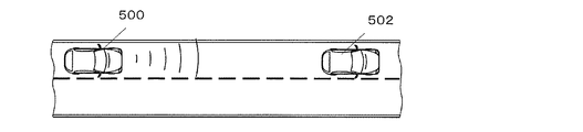
図25は、自車両500と、自車両500と同じ車線を走行している先行車両502とを示す。自車両500は、上述した実施形態にアレーアンテナを有する車載レーダシステムを備えている。自車両500の車載レーダシステムが高周波の送信信号を放射すると、その送信信号は先行車両502に到達して先行車両502で反射され、その一部は再び自車両500に戻る。車載レーダシステムは、その信号を受信して、先行車両502の位置、先行車両502までの距離、速度等を算出する。
FIG. 25 shows a
図26は、自車両500の車載レーダシステム510を示す。車載レーダシステム510は車内に配置されている。より具体的には、車載レーダシステム510は、リアビューミラーの鏡面と反対側の面に配置されている。車載レーダシステム510は、車内から車両500の進行方向に向けて高周波の送信信号を放射し、進行方向から到来した信号を受信する。
FIG. 26 shows an on-
本応用例による車載レーダシステム510は、上記の実施形態2におけるアレーアンテナを有している。本応用例では、複数の導波部材の各々が延びる方向が鉛直方向に一致し、複数の導波部材の配列方向が水平方向に一致するように配置される。このため、複数のスロットを正面から見たときの横方向の寸法を小さくできる。上述のアレーアンテナを含むアンテナ装置の寸法の一例は、横×縦×奥行きが、60×30×10mmである。76GHz帯のミリ波レーダシステムのサイズとしては非常に小型であることが理解される。
The on-
なお、従来の多くの車載レーダシステムは、車外、たとえばフロントノーズの先端部に設置されている。その理由は、車載レーダシステムのサイズが比較的大きく、本開示のように車内に設置することが困難であるからである。本応用例による車載レーダシステム510は、前述のように車内に設置できるが、フロントノーズの先端に搭載してもよい。フロントノーズにおいて、車載レーダシステムが占める領域を減少させられるため、他の部品の配置が容易になる。
Many conventional on-vehicle radar systems are installed outside the vehicle, for example, at the tip of the front nose. The reason is that the size of the on-vehicle radar system is relatively large and it is difficult to install in the vehicle as in the present disclosure. The on-
本応用例によれば、送信アンテナに用いられる複数の導波部材(リッジ)の間隔を狭くすることができるため、隣接する複数の導波部材に対向して設けられる複数のスロットの間隔も狭くすることができる。これにより、グレーティングローブの影響を抑制することができる。たとえば、横方向に隣接する2つのスロットの中心間隔を送信波の自由空間波長λoよりも短く(約4mm未満に)した場合にはグレーティングローブは前方には発生しない。これにより、グレーティングローブの影響を抑制できる。なお、グレーティングローブは、アンテナ素子の配列間隔が電磁波の波長の半分よりも大きくなると出現する。しかし、配列間隔が波長未満であればグレーティングローブは前方には現れない。このため、アレーアンテナを構成する各アンテナ素子から放射される電波に位相差を付与するビームステアリングを行わない場合は、アンテナ素子の配置間隔が波長よりも小さければ、グレーティングローブは実質的には影響しない。送信アンテナのアレーファクタを調整することにより、送信アンテナの指向性を調整することができる。複数の導波部材上を伝送される電磁波の位相を個別に調整できるように、位相シフタを設けてもよい。この場合は、グレーティングローブの影響を避けるために、アンテナ素子の配置間隔は送信波の自由空間波長λoの半分未満とする事がより好ましい。位相シフタを設けることにより、送信アンテナの指向性を任意の方向に変更することができる。位相シフタの構成は周知であるため、その構成の説明は省略する。 According to this application example, since the distance between the plurality of waveguide members (ridges) used for the transmitting antenna can be narrowed, the distance between the plurality of slots provided facing the plurality of adjacent waveguide members is also narrow. can do. Thereby, the influence of the grating lobe can be suppressed. For example, when the center distance between two laterally adjacent slots is shorter than the free space wavelength λo of the transmission wave (less than about 4 mm), grating lobes do not occur forward. This can suppress the influence of grating lobes. The grating lobes appear when the array spacing of the antenna elements is larger than half the wavelength of the electromagnetic wave. However, if the array spacing is less than the wavelength, the grating lobes do not appear forward. For this reason, when beam steering for giving a phase difference to radio waves radiated from each antenna element constituting the array antenna is not performed, the grating lobe substantially affects if the arrangement distance between the antenna elements is smaller than the wavelength. do not do. By adjusting the array factor of the transmitting antenna, the directivity of the transmitting antenna can be adjusted. A phase shifter may be provided so that the phases of the electromagnetic waves transmitted on the plurality of waveguide members can be adjusted individually. In this case, in order to avoid the influence of the grating lobes, it is more preferable that the arrangement interval of the antenna elements be less than half of the free space wavelength λo of the transmission wave. By providing the phase shifter, the directivity of the transmitting antenna can be changed in any direction. Since the configuration of the phase shifter is well known, the description of the configuration is omitted.
本応用例における受信アンテナは、グレーティングローブに由来する反射波の受信を低減できるため、以下に説明する処理の精度を向上させることができる。以下、受信処理の一例を説明する。 The receiving antenna in this application example can reduce the reception of the reflected wave derived from the grating lobe, so that the accuracy of the processing described below can be improved. Hereinafter, an example of the reception process will be described.
図27Aは、車載レーダシステム510のアレーアンテナAAと、複数の到来波k(k:1〜Kの整数;以下同じ。Kは異なる方位に存在する物標の数。)との関係を示している。アレーアンテナAAは、直線状に配列されたM個のアンテナ素子を有する。原理上、アンテナは送信および受信の両方に利用することが可能であるため、アレーアンテナAAは送信アンテナおよび受信アンテナの両方を含み得る。以下では受信アンテナが受信した到来波を処理する方法の例を説明する。
FIG. 27A shows the relationship between the array antenna AA of the on-
アレーアンテナAAは、様々な角度から同時に入射する複数の到来波を受ける。複数の到来波の中には、同じ車載レーダシステム510の送信アンテナから放射され、物標で反射された到来波が含まれる。さらに、複数の到来波の中には、他の車両から放射された直接的または間接的な到来波も含まれる。
The array antenna AA receives a plurality of incoming waves simultaneously incident from various angles. The plurality of incoming waves include the incoming waves emitted from the transmitting antenna of the same on-
到来波の入射角度(すなわち到来方向を示す角度)は、アレーアンテナAAのブロードサイドBを基準とする角度を表している。到来波の入射角度は、アンテナ素子群が並ぶ直線方向に垂直な方向に対する角度を表す。 The incident angle of the incoming wave (ie, the angle indicating the incoming direction) represents an angle based on the broadside B of the array antenna AA. The incident angle of the incoming wave represents an angle with respect to the direction perpendicular to the linear direction in which the antenna element groups are arranged.
いま、k番目の到来波に注目する。「k番目の到来波」とは、異なる方位に存在するK個の物標からアレーアンテナにK個の到来波が入射しているときにおける、入射角θkによって識別される到来波を意味する。 Now, we focus on the k th arrival wave. “K-th incoming wave” means an incoming wave identified by the incident angle θ k when K incoming waves are incident on the array antenna from K targets present in different orientations .
図27Bは、k番目の到来波を受信するアレーアンテナAAを示している。アレーアンテナAAが受信した信号は、M個の要素を持つ「ベクトル」として、数1のように表現できる。
FIG. 27B shows the array antenna AA that receives the k-th incoming wave. A signal received by the array antenna AA can be expressed as
(数1)
S=[s1,s2,…,sM]T
ここで、sm(m:1〜Mの整数;以下同じ。)は、m番目のアンテナ素子が受信した信号の値である。上付きのTは転置を意味する。Sは列ベクトルである。列ベクトルSは、アレーアンテナの構成によって決まる方向ベクトル(ステアリングベクトルまたはモードベクトルと称する。)と、物標(波源または信号源とも称する。)における信号を示す複素ベクトルとの積によって与えられる。波源の個数がKであるとき、各波源から個々のアンテナ素子に到来する信号の波が線形的に重畳される。このとき、smは数2のように表現できる。
(1)
S = [s 1 , s 2 , ..., s M ] T
Here, s m (m is an integer from 1 to M; the same applies hereinafter) is the value of the signal received by the m-th antenna element. Superscript T means transposition. S is a column vector. The column vector S is given by the product of a direction vector (referred to as a steering vector or mode vector) determined by the configuration of the array antenna and a complex vector representing a signal on a target (also referred to as a wave source or signal source). When the number of wave sources is K, waves of signals arriving from each wave source to the individual antenna elements are linearly superimposed. At this time, s m can be expressed as equation 2.
数2から理解されるように、smは、実部(Re)と虚部(Im)とから構成される複素数として表現されている。 As understood from the equation 2, s m is expressed as a complex number composed of real part (Re) and imaginary part (Im).
ノイズ(内部雑音または熱雑音)を考慮してさらに一般化すると、アレー受信信号Xは数3のように表現できる。 Further generalizing in consideration of noise (internal noise or thermal noise), the array reception signal X can be expressed as Equation 3.
(数3)
X=S+N
Nはノイズのベクトル表現である。
(Number 3)
X = S + N
N is a vector representation of noise.
信号処理回路は、数3に示されるアレー受信信号Xを用いて到来波の自己相関行列Rxx(数4)を求め、さらに自己相関行列Rxxの各固有値を求める。 The signal processing circuit obtains an autocorrelation matrix Rxx (Equation 4) of the incoming wave using the array reception signal X shown in Equation 3, and further obtains each eigenvalue of the autocorrelation matrix Rxx.
求めた複数の固有値のうち、熱雑音によって定まる所定値以上の値を有する固有値(信号空間固有値)の個数が、到来波の個数に対応する。そして、反射波の到来方向の尤度が最も大きくなる(最尤度となる)角度を算出することにより、物標の数および各物標が存在する角度を特定することができる。この処理は、最尤推定法として公知である。 The number of eigenvalues (signal space eigenvalues) having a value equal to or greater than a predetermined value determined by the thermal noise among the plurality of eigenvalues determined corresponds to the number of arrival waves. Then, the number of targets and the angle at which each target exists can be specified by calculating the angle at which the likelihood of the direction of arrival of the reflected wave is the largest (the maximum likelihood). This process is known as maximum likelihood estimation.
次に、図28を参照する。図28は、本開示による車両走行制御装置600の基本構成の一例を示すブロック図である。図28に示される車両走行制御装置600は、車両に実装されたレーダシステム510と、レーダシステム510に接続された走行支援電子制御装置520とを備えている。レーダシステム510は、アレーアンテナAAと、レーダ信号処理装置530とを有している。
Next, FIG. 28 is referred to. FIG. 28 is a block diagram showing an example of a basic configuration of a vehicle
アレーアンテナAAは、複数のアンテナ素子を有しており、その各々が1個または複数個の到来波に応答して受信信号を出力する。上述のように、アレーアンテナAAは高周波のミリ波を放射することも可能である。なお、アレーアンテナAAは、実施形態2におけるアレーアンテナに限らず、受信に適した他のアレーアンテナであってもよい。 The array antenna AA has a plurality of antenna elements, each of which outputs a received signal in response to one or more incoming waves. As described above, the array antenna AA can also emit high frequency millimeter waves. The array antenna AA is not limited to the array antenna in the second embodiment, and may be another array antenna suitable for reception.
レーダシステム510のうち、アレーアンテナAAは車両に取り付けられる必要がある。しかしながらレーダ信号処理装置530の少なくとも一部の機能は、車両走行制御装置600の外部(例えば自車両の外)に設けられたコンピュータ550およびデータベース552によって実現されてもよい。その場合、レーダ信号処理装置530のうちで車両内に位置する部分は、車両の外部に設けられたコンピュータ550およびデータベース552に、信号またはデータの双方向通信が行えるように、常時または随時に接続され得る。通信は、車両が備える通信デバイス540、および一般の通信ネットワークを介して行われる。
Of the
データベース552は、各種の信号処理アルゴリズムを規定するプログラムを格納していても良い。レーダシステム510の動作に必要なデータおよびプログラムの内容は、通信デバイス540を介して外部から更新され得る。このように、レーダシステム510の少なくとも一部の機能は、クラウドコンピューティングの技術により、自車両の外部(他の車両の内部を含む)において実現し得る。したがって、本開示における「車載」のレーダシステムは、構成要素のすべてが車両に搭載されていることを必要としない。ただし、本願では、簡単のため、特に断らない限り、本開示の構成要素のすべてが1台の車両(自車両)に搭載されている形態を説明する。
The
レーダ信号処理装置530は、信号処理回路560を有している。この信号処理回路560は、アレーアンテナAAから直接または間接に受信信号を受け取り、受信信号、または受信信号から生成した二次信号を到来波推定ユニットAUに入力する。受信信号から二次信号を生成する回路(不図示)の一部または全部は、信号処理回路560の内部に設けられている必要はない。このような回路(前処理回路)の一部または全部は、アレーアンテナAAとレーダ信号処理装置530との間に設けられていても良い。
The radar
信号処理回路560は、受信信号または二次信号を用いて演算を行い、到来波の個数を示す信号を出力するように構成されている。ここで、「到来波の個数を示す信号」は、自車両の前方を走行する1または複数の先行車両の数を示す信号ということができる。
The
この信号処理回路560は、公知のレーダ信号処理装置が実行する各種の信号処理を実行するように構成されていればよい。例えば、信号処理回路560は、MUSIC法、ESPRIT法、およびSAGE法などの「超分解能アルゴリズム」(スーパーレゾリューション法)、または相対的に分解能が低い他の到来方向推定アルゴリズムを実行するように構成され得る。
The
図28に示す到来波推定ユニットAUは、任意の到来方向推定アルゴリズムにより、到来波の方位を示す角度を推定し、推定結果を示す信号を出力する。信号処理回路560は、到来波推定ユニットAUが実行する公知のアルゴリズムにより、到来波の波源である物標までの距離、物標の相対速度、物標の方位を推定し、推定結果を示す信号を出力する。
The arrival wave estimation unit AU shown in FIG. 28 estimates an angle indicating the direction of the arrival wave by an arbitrary arrival direction estimation algorithm, and outputs a signal indicating the estimation result. The
本開示における「信号処理回路」の用語は、単一の回路に限られず、複数の回路の組み合わせを概念的に一つの機能部品として捉えた態様も含む。信号処理回路560は、1個または複数のシステムオンチップ(SoC)によって実現されても良い。例えば、信号処理回路560の一部または全部がプログラマブルロジックデバイス(PLD)であるFPGA(Field−Programmable Gate Array)であってもよい。その場合、信号処理回路560は、複数の演算素子(例えば汎用ロジックおよびマルチプライヤ)および複数のメモリ素子(例えばルックアップテーブルまたはメモリブロック)を含む。または、信号処理回路560は、汎用プロセッサおよびメインメモリ装置の集合であってもよい。信号処理回路560は、プロセッサコアとメモリとを含む回路であってもよい。これらは信号処理回路560として機能し得る。
The term “signal processing circuit” in the present disclosure is not limited to a single circuit, but also includes an aspect in which a combination of a plurality of circuits is conceptually regarded as one functional component. The
走行支援電子制御装置520は、レーダ信号処理装置530から出力される各種の信号に基づいて車両の走行支援を行うように構成されている。走行支援電子制御装置520は、所定の機能を発揮するように各種の電子制御ユニットに指示を行う。所定の機能は、例えば、先行車両までの距離(車間距離)が予め設定された値よりも短くなったときに警報を発してドライバにブレーキ操作を促す機能、ブレーキを制御する機能、アクセルを制御する機能を含む。例えば、自車両のアダプティブクルーズコントロールを行う動作モードのとき、走行支援電子制御装置520は、各種の電子制御ユニット(不図示)およびアクチュエータに所定の信号を送り、自車両から先行車両までの距離を予め設定された値に維持したり、自車両の走行速度を予め設定された値に維持したりする。
The driving support
MUSIC法による場合、信号処理回路560は、自己相関行列の各固有値を求め、それらのうちの熱雑音によって定まる所定値(熱雑音電力)より大きい固有値(信号空間固有値)の個数を示す信号を、到来波の個数を示す信号として出力する。
In the case of the MUSIC method, the
次に、図29を参照する。図29は、車両走行制御装置600の構成の他の例を示すブロック図である。図29の車両走行制御装置600におけるレーダシステム510は、受信専用のアレーアンテナ(受信アンテナとも称する。)Rxおよび送信専用のアレーアンテナ(送信アンテナとも称する。)Txを含むアレーアンテナAAと、物体検知装置570とを有している。
Next, FIG. 29 is referred to. FIG. 29 is a block diagram showing another example of the configuration of vehicle
送信アンテナTxおよび受信アンテナRxの少なくとも一方は、上述した導波路構造を有している。送信アンテナTxは、例えばミリ波である送信波を放射する。受信専用の受信アンテナRxは、1個または複数個の到来波(例えばミリ波)に応答して受信信号を出力する。 At least one of the transmitting antenna Tx and the receiving antenna Rx has the above-described waveguide structure. The transmission antenna Tx radiates a transmission wave which is, for example, a millimeter wave. The receive-only receive antenna Rx outputs a receive signal in response to one or more incoming waves (e.g., millimeter waves).
送受信回路580は、送信波のための送信信号を送信アンテナTxに送り、また、受信アンテナRxで受けた受信波による受信信号の「前処理」を行う。前処理の一部または全部は、レーダ信号処理装置530の信号処理回路560によって実行されても良い。送受信回路580が行う前処理の典型的な例は、受信信号からビート信号を生成すること、および、アナログ形式の受信信号をデジタル形式の受信信号に変換することを含み得る。
The transmission /
なお、本開示によるレーダシステムは、車両に搭載される形態の例に限定されず、道路または建物に固定されて使用され得る。 In addition, the radar system according to the present disclosure is not limited to an example of a form mounted on a vehicle, and may be fixed to a road or a building and used.
続いて、車両走行制御装置600のより具体的な構成の例を説明する。
Subsequently, an example of a more specific configuration of the vehicle
図30は、車両走行制御装置600のより具体的な構成の例を示すブロック図である。図30に示される車両走行制御装置600は、レーダシステム510と、車載カメラシステム700とを備えている。レーダシステム510は、アレーアンテナAAと、アレーアンテナAAに接続された送受信回路580と、信号処理回路560とを有している。
FIG. 30 is a block diagram showing an example of a more specific configuration of the vehicle
車載カメラシステム700は、車両に搭載される車載カメラ710と、車載カメラ710によって取得された画像または映像を処理する画像処理回路720とを有している。
The on-
本応用例における車両走行制御装置600は、アレーアンテナAAおよび車載カメラ710に接続された物体検知装置570と、物体検知装置570に接続された走行支援電子制御装置520とを備えている。この物体検知装置570は、前述したレーダ信号処理装置530(信号処理回路560を含む)に加えて、送受信回路580および画像処理回路720を含んでいる。物体検知装置570は、レーダシステム510によって得られる情報だけではなく、画像処理回路720によって得られる情報を利用して、道路上または道路近傍における物標を検知することができる。例えば自車両が同一方向の2本以上の車線のいずれかを走行している最中において、自車両が走行している車線がいずれの車線であるかを、画像処理回路720によって判別し、その判別の結果を信号処理回路560に与えることができる。信号処理回路560は、所定の到来方向推定アルゴリズム(たとえばMUSIC法)によって先行車両の数および方位を認識するとき、画像処理回路720からの情報を参照することにより、先行車両の配置について、より信頼度の高い情報を提供することが可能になる。
The vehicle
なお、車載カメラシステム700は、自車両が走行している車線がいずれの車線であるかを特定する手段の一例である。他の手段を利用して自車両の車線位置を特定してもよい。例えば、超広帯域無線(UWB:Ultra Wide Band)を利用して、複数車線のどの車線を自車両が走行しているかを特定することができる。超広帯域無線が位置測定および/またはレーダとして利用可能なことは広く知られている。超広帯域無線を利用すれば、レーダの距離分解能が高まるため、前方に多数の車両が存在する場合でも、距離の差に基づいて個々の物標を区別して検知できる。このため、路肩のガードレール、または中央分離帯からの距離を特定することが可能である。各車線の幅は、各国の法律等で予め定められている。これらの情報を利用して、自車両が現在走行中の車線の位置を特定することができる。なお、超広帯域無線は一例である。他の無線による電波を利用してもよい。また、ライダー(LIDAR:Light Detection and Ranging)をレーダと組合せて用いてもよい。LIDARは、レーザレーダと呼ばれることもある。
The on-
アレーアンテナAAは、一般的な車載用ミリ波アレーアンテナであり得る。本応用例における送信アンテナTxは、ミリ波を送信波として車両の前方に放射する。送信波の一部は、典型的には先行車両である物標によって反射される。これにより、物標を波源とする反射波が発生する。反射波の一部は、到来波としてアレーアンテナ(受信アンテナ)AAに到達する。アレーアンテナAAを構成している複数のアンテナ素子の各々は、1個または複数個の到来波に応答して、受信信号を出力する。反射波の波源として機能する物標の個数がK個(Kは1以上の整数)である場合、到来波の個数はK個であるが、到来波の個数Kは既知ではない。 The array antenna AA can be a general automotive millimeter-wave array antenna. The transmission antenna Tx in this application example radiates a millimeter wave as a transmission wave to the front of the vehicle. A portion of the transmitted wave is reflected by a target that is typically a leading vehicle. Thereby, the reflected wave which makes a target a wave source is generated. A part of the reflected wave reaches the array antenna (receiving antenna) AA as an incoming wave. Each of the plurality of antenna elements constituting the array antenna AA outputs a received signal in response to one or more incoming waves. In the case where the number of targets serving as a source of reflected waves is K (K is an integer of 1 or more), the number of incoming waves is K, but the number K of incoming waves is not known.
図28の例では、レーダシステム510はアレーアンテナAAも含めて一体的にリアビューミラーに配置されるとした。しかしながら、アレーアンテナAAの個数および位置は、特定の個数および特定の位置に限定されない。アレーアンテナAAは、車両の後方に位置する物標を検知できるように車両の後面に配置されてもよい。また、車両の前面または後面に複数のアレーアンテナAAが配置されていても良い。アレーアンテナAAは、車両の室内に配置されていても良い。アレーアンテナAAとして、各アンテナ素子が上述したホーンを有するホーンアンテナが採用される場合でも、そのようなアンテナ素子を備えるアレーアンテナは車両の室内に配置され得る。
In the example of FIG. 28, the
信号処理回路560は、受信アンテナRxによって受信され、送受信回路580によって前処理された受信信号を受け取り、処理する。この処理は、受信信号を到来波推定ユニットAUに入力すること、または、受信信号から二次信号を生成して二次信号を到来波推定ユニットAUに入力すること、を含む。
図30の例では、信号処理回路560から出力される信号および画像処理回路720から出力される信号を受け取る選択回路596が物体検知装置570内に設けられている。選択回路596は、信号処理回路560から出力される信号および画像処理回路720から出力される信号の一方または両方を走行支援電子制御装置520に与える。
In the example of FIG. 30, a
図31は、本応用例におけるレーダシステム510のより詳細な構成例を示すブロック図である。
FIG. 31 is a block diagram showing a more detailed configuration example of the
図31に示すように、アレーアンテナAAは、ミリ波の送信を行う送信アンテナTxと、物標で反射された到来波を受信する受信アンテナRxとを備えている。図面上では送信アンテナTxは1つであるが、特性の異なる2種類以上の送信アンテナが設けられていてもよい。アレーアンテナAAは、M個(Mは3以上の整数)のアンテナ素子111、112、・・・、11Mを備えている。複数のアンテナ素子111、112、・・・、11Mの各々は、到来波に応答して、受信信号s1、s2、・・・、sM(図27B)を出力する。
As shown in FIG. 31, the array antenna AA includes a transmitting antenna Tx that transmits a millimeter wave, and a receiving antenna Rx that receives an incoming wave reflected by a target. Although one transmission antenna Tx is shown in the drawing, two or more types of transmission antennas having different characteristics may be provided. Array antenna AA is the
アレーアンテナAAにおいて、アンテナ素子111〜11Mは、例えば、固定された間隔を空けて直線状または面状に配列されている。到来波は、アンテナ素子111〜11Mが配列されている面の法線に対する角度θの方向からアレーアンテナAAに入射する。このため、到来波の到来方向は、この角度θによって規定される。
In the array antenna AA, for example, the
1個の物標からの到来波がアレーアンテナAAに入射するとき、アンテナ素子111〜11Mには、同一の角度θの方位から平面波が入射すると近似できる。異なる方位にあるK個の物標からアレーアンテナAAにK個の到来波が入射しているとき、相互に異なる角度θ1〜θKによって個々の到来波を識別することができる。
When an incoming wave from one target is incident on the array antenna AA, it can be approximated that plane waves are incident on the
図31に示されるように、物体検知装置570は、送受信回路580と信号処理回路560とを含む。
As shown in FIG. 31, the
送受信回路580は、三角波生成回路581、VCO(Voltage−Controlled−Oscillator:電圧制御可変発振器)582、分配器583、ミキサ584、フィルタ585、スイッチ586、A/Dコンバータ587、制御器588を備える。本応用例におけるレーダシステムは、FMCW方式でミリ波の送受信を行うように構成されているが、本開示のレーダシステムは、この方式に限定されない。送受信回路580は、アレーアンテナAAからの受信信号と送信アンテナTxのための送信信号とに基づいて、ビート信号を生成するように構成されている。
The transmission /
信号処理回路560は、距離検出部533、速度検出部534、方位検出部536を備える。信号処理回路560は、送受信回路580のA/Dコンバータ587からの信号を処理し、検出された物標までの距離、物標の相対速度、物標の方位を示す信号をそれぞれ出力するように構成されている。
The
まず、送受信回路580の構成および動作を詳細に説明する。
First, the configuration and operation of the transmission /
三角波生成回路581は三角波信号を生成し、VCO582に与える。VCO582は、三角波信号に基づいて変調された周波数を有する送信信号を出力する。図32は、三角波生成回路581が生成した信号に基づいて変調された送信信号の周波数変化を示している。この波形の変調幅はΔf、中心周波数はf0である。このようにして周波数が変調された送信信号は分配器583に与えられる。分配器583は、VCO582から得た送信信号を、各ミキサ584および送信アンテナTxに分配する。こうして、送信アンテナは、図32に示されるように三角波状に変調された周波数を有するミリ波を放射する。
The triangular
図32には、送信信号に加えて、単一の先行車両で反射された到来波による受信信号の例が記載されている。受信信号は、送信信号に比べて遅延している。この遅延は、自車両と先行車両との距離に比例している。また、受信信号の周波数は、ドップラー効果により、先行車両の相対速度に応じて増減する。 FIG. 32 shows an example of a received signal by an incoming wave reflected by a single preceding vehicle in addition to the transmitted signal. The received signal is delayed relative to the transmitted signal. This delay is proportional to the distance between the host vehicle and the preceding vehicle. Also, the frequency of the received signal increases or decreases according to the relative velocity of the preceding vehicle due to the Doppler effect.
受信信号と送信信号とを混合すると、周波数の差異に基づいてビート信号が生成される。このビート信号の周波数(ビート周波数)は、送信信号の周波数が増加する期間(上り)と、送信信号の周波数が減少する期間(下り)とで異なる。各期間におけるビート周波数が求められると、それらのビート周波数に基づいて、物標までの距離と、物標の相対速度が算出される。 Mixing the receive and transmit signals produces a beat signal based on the frequency difference. The frequency (beat frequency) of this beat signal differs between the period (uplink) in which the frequency of the transmission signal increases and the period (downlink) in which the frequency of the transmission signal decreases. When the beat frequency in each period is determined, the distance to the target and the relative velocity of the target are calculated based on the beat frequency.
図33は、「上り」の期間におけるビート周波数fu、および「下り」の期間におけるビート周波数fdを示している。図33のグラフにおいて、横軸が周波数、縦軸が信号強度である。このようなグラフは、ビート信号の時間−周波数変換を行うことによって得られる。ビート周波数fu、fdが得られると、公知の式に基づいて、物標までの距離と、物標の相対速度が算出される。本応用例では、以下に説明する構成および動作により、アレーアンテナAAの各アンテナ素子に対応したビート周波数を求め、それに基づいて物標の位置情報を推定することが可能になる。 FIG. 33 shows the beat frequency fu in the “uplink” period and the beat frequency fd in the “downlink” period. In the graph of FIG. 33, the horizontal axis is frequency, and the vertical axis is signal intensity. Such a graph is obtained by performing time-frequency conversion of the beat signal. When the beat frequencies fu and fd are obtained, the distance to the target and the relative velocity of the target are calculated based on known equations. In this application example, it becomes possible to obtain the beat frequency corresponding to each antenna element of the array antenna AA and to estimate the position information of the target based on the configuration and operation described below.
図31に示される例において、各アンテナ素子111〜11Mに対応したチャンネルCh1〜ChMからの受信信号は、増幅器によって増幅され、対応するミキサ584に入力される。ミキサ584の各々は、増幅された受信信号に送信信号を混合する。この混合により、受信信号と送信信号との間にある周波数差に対応したビート信号が生成される。生成されたビート信号は、対応するフィルタ585に与えられる。フィルタ585は、チャンネルCh1〜ChMのビート信号の帯域制限を行い、帯域制限されたビート信号をスイッチ586に与える。
In the example shown in FIG. 31, the received signal from the channel Ch 1 to CH M corresponding to each
スイッチ586は、制御器588から入力されるサンプリング信号に応答してスイッチングを実行する。制御器588は、例えばマイクロコンピュータによって構成され得る。制御器588は、ROMなどのメモリに格納されたコンピュータプログラムに基づいて、送受信回路580の全体を制御する。制御器588は、送受信回路580の内部に設けられている必要は無く、信号処理回路560の内部に設けられていても良い。つまり、送受信回路580は信号処理回路560からの制御信号にしたがって動作してもよい。または、送受信回路580および信号処理回路560の全体を制御する中央演算ユニットなどによって、制御器588の機能の一部または全部が実現されていても良い。
The
フィルタ585の各々を通過したチャンネルCh1〜ChMのビート信号は、スイッチ586を介して、順次、A/Dコンバータ587に与えられる。A/Dコンバータ587は、スイッチ586から入力されるチャンネルCh1〜ChMのビート信号を、サンプリング信号に同期してデジタル信号に変換する。
The beat signals of the channels Ch 1 to Ch M passed through each of the
以下、信号処理回路560の構成および動作を詳細に説明する。本応用例では、FMCW方式によって、物標までの距離および物標の相対速度を推定する。レーダシステムは、以下に説明するFMCW方式に限定されず、2周波CWまたはスペクトル拡散などの他の方式を用いても実施可能である。
Hereinafter, the configuration and operation of the
図31に示される例において、信号処理回路560は、メモリ531、受信強度算出部532、距離検出部533、速度検出部534、DBF(デジタルビームフォーミング)処理部535、方位検出部536、物標引継ぎ処理部537、相関行列生成部538、物標出力処理部539および到来波推定ユニットAUを備えている。前述したように、信号処理回路560の一部または全部がFPGAによって実現されていてもよく、汎用プロセッサおよびメインメモリ装置の集合によって実現されていてもよい。メモリ531、受信強度算出部532、DBF処理部535、距離検出部533、速度検出部534、方位検出部536、物標引継ぎ処理部537、および到来波推定ユニットAUは、それぞれ、別個のハードウェアによって実現される個々の部品であってもよいし、1つの信号処理回路における機能上のブロックであってもよい。
In the example illustrated in FIG. 31, the
図34は、信号処理回路560がプロセッサPRおよびメモリ装置MDを備えるハードウェアによって実現されている形態の例を示している。このような構成を有する信号処理回路560も、メモリ装置MDに格納されたコンピュータプログラムの働きにより、図31に示す受信強度算出部532、DBF処理部535、距離検出部533、速度検出部534、方位検出部536、物標引継ぎ処理部537、相関行列生成部538、到来波推定ユニットAUの機能が果たされ得る。
FIG. 34 shows an example of a form in which the
本応用例における信号処理回路560は、デジタル信号に変換された各ビート信号を受信信号の二次信号として、先行車両の位置情報を推定し、推定結果を示す信号を出力するよう構成されている。以下、本応用例における信号処理回路560の構成および動作を詳細に説明する。
The
信号処理回路560内のメモリ531は、A/Dコンバータ587から出力されるデジタル信号をチャンネルCh1〜ChMごとに格納する。メモリ531は、例えば、半導体メモリ、ハードディスクおよび/または光ディスクなどの一般的な記憶媒体によって構成され得る。
The
受信強度算出部532は、メモリ531に格納されたチャンネルCh1〜ChMごとのビート信号(図32の下図)に対してフーリエ変換を行う。本明細書では、フーリエ変換後の複素数データの振幅を「信号強度」と称する。受信強度算出部532は、複数のアンテナ素子のいずれかの受信信号の複素数データ、または、複数のアンテナ素子のすべての受信信号の複素数データの加算値を周波数スペクトルに変換する。こうして得られたスペクトルの各ピーク値に対応するビート周波数、すなわち距離に依存した物標(先行車両)の存在を検出することができる。全アンテナ素子の受信信号の複素数データを加算すると、ノイズ成分が平均化されるため、S/N比が向上する。
Reception
物標、すなわち先行車両が1個の場合、フーリエ変換の結果、図33に示されるように、周波数が増加する期間(「上り」の期間)および減少する期間(「下り」の期間)に、それぞれ、1個のピーク値を有するスペクトルが得られる。「上り」の期間におけるピーク値のビート周波数を「fu」、「下り」の期間におけるピーク値のビート周波数を「fd」とする。 In the case where there is one target vehicle, ie, one preceding vehicle, as a result of Fourier transform, as shown in FIG. 33, a period during which the frequency increases (period of “up”) and during a period of decrease (period of “down”) In each case, a spectrum having one peak value is obtained. The beat frequency of the peak value in the "uplink" period is "fu", and the beat frequency of the peak value in the "downlink" period is "fd".
受信強度算出部532は、ビート周波数毎の信号強度から、予め設定された数値(閾値)を超える信号強度を検出することによって、物標が存在していることを判定する。受信強度算出部532は、信号強度のピークを検出した場合、ピーク値のビート周波数(fu、fd)を対象物周波数として距離検出部533、速度検出部534へ出力する。受信強度算出部532は、周波数変調幅Δfを示す情報を距離検出部533へ出力し、中心周波数f0を示す情報を速度検出部534へ出力する。
The reception
受信強度算出部532は、複数の物標に対応する信号強度のピークが検出された場合には、上りのピーク値と下りのピーク値とを予め定められた条件によって対応づける。同一の物標からの信号と判断されたピークに同一の番号を付与し、距離検出部533および速度検出部534に与える。
When peaks of signal strength corresponding to a plurality of targets are detected, the reception
複数の物標が存在する場合、フーリエ変換後、ビート信号の上り部分とビート信号の下り部分のそれぞれに物標の数と同じ数のピークが表れる。レーダと物標の距離に比例して、受信信号が遅延し、図32における受信信号は右方向にシフトするので、レーダと物標との距離が離れるほど、ビート信号の周波数は、大きくなる。 When a plurality of targets are present, after Fourier transformation, the same number of peaks as the number of targets appear in the upstream portion of the beat signal and the downstream portion of the beat signal. Since the received signal is delayed in proportion to the distance between the radar and the target and the received signal in FIG. 32 is shifted to the right, the frequency of the beat signal increases as the distance between the radar and the target increases.
距離検出部533は、受信強度算出部532から入力されるビート周波数fu、fdに基づいて、下記の式により距離Rを算出し、物標引継ぎ処理部537へ与える。
The
R={c・T/(2・Δf)}・{(fu+fd)/2}
また、速度検出部534は、受信強度算出部532から入力されるビート周波数fu、fdに基づいて、下記の式によって相対速度Vを算出し、物標引継ぎ処理部537へ与える。
R = {c · T / (2 · Δf)} · {(fu + fd) / 2}
Further, the
V={c/(2・f0)}・{(fu−fd)/2}
距離Rおよび相対速度Vを算出する式において、cは光速、Tは変調周期である。
V = {c / (2 · f0)} · {(fu−fd) / 2}
In the equation for calculating the distance R and the relative velocity V, c is the speed of light, and T is the modulation period.
なお、距離Rの分解能下限値は、c/(2Δf)で表される。したがって、Δfが大きくなるほど、距離Rの分解能が高まる。周波数f0が76GHz帯の場合において、Δfを660メガヘルツ(MHz)程度に設定するとき、距離Rの分解能は例えば0.23メートル(m)程度である。このため、2台の先行車両が併走しているとき、FMCW方式では車両が1台なのか2台なのかを識別することは困難である場合がある。このような場合、角度分解能が極めて高い到来方向推定アルゴリズムを実行すれば、2台の先行車両の方位を分離して検出することが可能である。 The resolution lower limit value of the distance R is expressed by c / (2Δf). Therefore, the resolution of the distance R increases as Δf increases. When the frequency f0 is in the 76 GHz band and the Δf is set to about 660 megahertz (MHz), the resolution of the distance R is, for example, about 0.23 meters (m). For this reason, when two leading vehicles run in parallel, it may be difficult to identify whether one or two vehicles are present in the FMCW method. In such a case, it is possible to separate and detect the directions of two preceding vehicles by executing an arrival direction estimation algorithm with a very high angular resolution.
DBF処理部535は、アンテナ素子111、112、・・・、11Mにおける信号の位相差を利用して、入力される各アンテナに対応した時間軸でフーリエ変換された複素データを、アンテナ素子の配列方向にフーリエ変換する。そして、DBF処理部535は、角度分解能に対応した角度チャネル毎のスペクトルの強度を示す空間複素数データを算出し、ビート周波数毎に方位検出部536に出力する。
The
方位検出部536は、先行車両の方位を推定するために設けられている。方位検出部536は、算出されたビート周波数毎の空間複素数データの値の大きさのうち、一番大きな値を取る角度θを対象物が存在する方位として物標引継ぎ処理部537に出力する。
The
なお、到来波の到来方向を示す角度θを推定する方法は、この例に限定されない。前述した種々の到来方向推定アルゴリズムを用いて行うことができる。 Note that the method of estimating the angle θ indicating the arrival direction of the incoming wave is not limited to this example. It can be performed using the various direction of arrival estimation algorithms described above.
物標引継ぎ処理部537は、今回算出した対象物の距離、相対速度、方位の値と、メモリ531から読み出した1サイクル前に算出された対象物の距離、相対速度、方位の値とのそれぞれの差分の絶対値を算出する。そして、差分の絶対値が、それぞれの値毎に決められた値よりも小さいとき、物標引継ぎ処理部537は、1サイクル前に検知した物標と今回検知した物標とを同じものと判定する。その場合、物標引継ぎ処理部537は、メモリ531から読み出したその物標の引継ぎ処理回数を1つだけ増やす。
The
物標引継ぎ処理部537は、差分の絶対値が決められた値よりも大きな場合には、新しい対象物を検知したと判断する。物標引継ぎ処理部537は、今回の対象物の距離、相対速度、方位およびその対象物の物標引継ぎ処理回数をメモリ531に保存する。
If the absolute value of the difference is larger than the determined value, the target
信号処理回路560で、受信した反射波を基にして生成された信号であるビート信号を周波数解析して得られるスペクトラムを用い、対象物との距離、相対速度を検出することができる。
The
相関行列生成部538は、メモリ531に格納されたチャンネルCh1〜ChMごとのビート信号(図32の下図)を用いて自己相関行列を求める。数4の自己相関行列において、各行列の成分は、ビート信号の実部および虚部によって表現される値である。相関行列生成部538は、さらに自己相関行列Rxxの各固有値を求め、得られた固有値の情報を到来波推定ユニットAUへ入力する。
The correlation
受信強度算出部532は、複数の対象物に対応する信号強度のピークが複数検出された場合、上りの部分および下りの部分のピーク値ごとに、周波数が小さいものから順番に番号をつけて、物標出力処理部539へ出力する。ここで、上りおよび下りの部分において、同じ番号のピークは、同じ対象物に対応しており、それぞれの識別番号を対象物の番号とする。なお、煩雑化を回避するため、図31では、受信強度算出部532から物標出力処理部539への引出線の記載は省略している。
When a plurality of peaks of signal strength corresponding to a plurality of objects are detected, the reception
物標出力処理部539は、対象物が前方構造物である場合に、その対象物の識別番号を物標として出力する。物標出力処理部539は、複数の対象物の判定結果を受け取り、そのどちらもが前方構造物である場合、自車両の車線上にある対象物の識別番号を物標が存在する物体位置情報として出力する。また、物標出力処理部539は、複数の対象物の判定結果を受け取り、そのどちらもが前方構造物である場合であって、2つ以上の対象物が自車両の車線上にある場合、メモリ531から読み出した物標引継ぎ処理回数が多い対象物の識別番号を物標が存在する物体位置情報として出力する。
The target
再び図30を参照し、車載レーダシステム510が図30に示す構成例に組み込まれた場合の例を説明する。画像処理回路720は、映像から物体の情報を取得し、その物体の情報から物標位置情報を検出する。画像処理回路720は、例えば、取得した映像内のオブジェクトの奥行き値を検出して物体の距離情報を推定したり、映像の特徴量から物体の大きさの情報等を検出したりすることにより、予め設定された物体の位置情報を検出するように構成されている。
Referring again to FIG. 30, an example in which the on-
選択回路596は、信号処理回路560および画像処理回路720から受け取った位置情報を選択的に走行支援電子制御装置520に与える。選択回路596は、例えば、信号処理回路560の物体位置情報に含まれている、自車両から検出した物体までの距離である第1距離と、画像処理回路720の物体位置情報に含まれている、自車両から検出した物体までの距離である第2距離とを比較してどちらが自車両に対して近距離であるかを判定する。例えば、判定された結果に基づいて、自車両に近いほうの物体位置情報を選択回路596が選択して走行支援電子制御装置520に出力し得る。なお、判定の結果、第1距離および第2距離が同じ値であった場合には、選択回路596は、そのいずれか一方または両方を走行支援電子制御装置520に出力し得る。
なお、物標出力処理部539(図31)は、受信強度算出部532から物標候補がないという情報が入力された場合には、物標なしとしてゼロを物体位置情報として出力する。そして、選択回路596は、物標出力処理部539からの物体位置情報に基づいて予め設定された閾値と比較することで信号処理回路560あるいは画像処理回路720の物体位置情報を使用するか選択している。
It should be noted that, when information indicating that there is no target candidate is input from the reception
物体検知装置570によって先行物体の位置情報を受け取った走行支援電子制御装置520は、予め設定された条件により、物体位置情報の距離や大きさ、自車両の速度、降雨、降雪、晴天などの路面状態等の条件と併せて、自車両を運転しているドライバに対して操作が安全あるいは容易となるような制御を行う。例えば、走行支援電子制御装置520は、物体位置情報に物体が検出されていない場合、予め設定されている速度までスピードを上げるようにアクセル制御回路526に制御信号を送り、アクセル制御回路526を制御してアクセルペダルを踏み込むことと同等の動作を行う。
The driving support
走行支援電子制御装置520は、物体位置情報に物体が検出されている場合において、自車両から所定の距離であることが分かれば、ブレーキバイワイヤ等の構成により、ブレーキ制御回路524を介してブレーキの制御を行う。すなわち、速度を落とし、車間距離を一定に保つように操作する。走行支援電子制御装置520は、物体位置情報を受けて、警告制御回路522に制御信号を送り、車内スピーカを介して先行物体が近づいていることをドライバに知らせるように音声またはランプの点灯を制御する。走行支援電子制御装置520は、先行車両の配置を含む物体位置情報を受けとり、予め設定された走行速度の範囲であれば、先行物体との衝突回避支援を行うために自動的にステアリングを左右どちらかに操作し易くするか、あるいは、強制的に車輪の方向を変更するようにステアリング側の油圧を制御することができる。
If an object is detected in the object position information, the driving support
物体検知装置570では、選択回路596が前回検出サイクルにおいて一定時間連続して検出していた物体位置情報のデータで、今回検出サイクルで検出できなかったデータに対して、カメラで検出したカメラ映像からの先行物体を示す物体位置情報が紐付けされれば、トラッキングを継続させる判断を行い、信号処理回路560からの物体位置情報を優先的に出力するようにしても構わない。
In the
信号処理回路560および画像処理回路720の出力を選択回路596に選択させるための具体的構成の例および動作の例は、米国特許第8446312号明細書、米国特許第8730096号明細書、および米国特許第8730099号明細書に開示されている。この公報の内容の全体をここに援用する。
Examples of specific configurations and examples of operations for causing the
[第1の変形例]
上記の応用例の車載用レーダシステムにおいて、周波数変調連続波FMCWの1回の周波数変調の(掃引)条件、つまり変調に要する時間幅(掃引時間)は、例えば1ミリ秒である。しかし、掃引時間を100マイクロ秒程度に短くすることもできる。
[First Modification]
In the on-vehicle radar system of the above application example, the (sweep) condition of one frequency modulation of the frequency modulated continuous wave FMCW, that is, the time width required for the modulation (sweep time) is, for example, 1 millisecond. However, the sweep time can be shortened to about 100 microseconds.
ただし、そのような高速の掃引条件を実現するためには、送信波の放射に関連する構成要素のみならず、当該掃引条件下での受信に関連する構成要素をも高速に動作させる必要が生じる。例えば、当該掃引条件下で高速に動作するA/Dコンバータ587(図31)を設ける必要がある。A/Dコンバータ587のサンプリング周波数は、例えば10MHzである。サンプリング周波数は10MHzよりも早くてもよい。
However, in order to realize such high-speed sweep conditions, not only components related to transmission wave radiation but also components related to reception under the sweep conditions need to be operated at high speed. . For example, it is necessary to provide an A / D converter 587 (FIG. 31) that operates at high speed under the sweep conditions. The sampling frequency of the A /
本変形例においては、ドップラーシフトに基づく周波数成分を利用することなく、物標との相対速度を算出する。本変形例では、掃引時間Tm=100マイクロ秒であり、非常に短い。検出可能なビート信号の最低周波数は1/Tmであるので、この場合は10kHzとなる。これは、およそ20m/秒の相対速度を持つ物標からの反射波のドップラーシフトに相当する。即ち、ドップラーシフトに頼る限り、これ以下の相対速度を検出することはできない。よって、ドップラーシフトに基づく計算方法とは異なる計算方法を採用することが好適である。 In this modification, the relative velocity with the target is calculated without using the frequency component based on the Doppler shift. In this modification, the sweep time Tm = 100 microseconds, which is very short. Since the lowest frequency of the detectable beat signal is 1 / Tm, it is 10 kHz in this case. This corresponds to the Doppler shift of the reflected wave from the target with a relative velocity of approximately 20 m / s. That is, as long as the Doppler shift is relied upon, a relative velocity lower than this can not be detected. Therefore, it is preferable to adopt a calculation method different from the calculation method based on the Doppler shift.
本変形例では、一例として、送信波の周波数が増加するアップビート区間で得られた、送信波と受信波との差の信号(アップビート信号)を利用する処理を説明する。FMCWの1回の掃引時間は100マイクロ秒で、波形は、アップビート(上り)部分のみからなる鋸歯形状である。即ち、本変形例において、三角波/CW波生成回路581が生成する信号波は鋸歯形状を有する。また、周波数の掃引幅は500MHzである。ドップラーシフトに伴うピークは利用しないので、アップビート信号とダウンビート信号を生成して双方のピークを利用する処理は行わず、何れか一方の信号のみで処理を行う。ここではアップビート信号を利用する場合について説明するが、ダウンビート信号を用いる場合も同様の処理を行うことができる。
In this modification, as an example, a process of using a signal (upbeat signal) of the difference between the transmission wave and the reception wave obtained in the upbeat section in which the frequency of the transmission wave is increased will be described. One sweep time of the FMCW is 100 microseconds, and the waveform is a sawtooth shape consisting only of the upbeat portion. That is, in the present modification, the signal wave generated by the triangular wave / CW
A/Dコンバータ587(図31)は、10MHzのサンプリング周波数で各アップビート信号をサンプリングして、数百個のデジタルデータ(以下「サンプリングデータ」と呼ぶ。)を出力する。サンプリングデータは、例えば、受信波が得られる時刻以後で、かつ、送信波の送信が終了した時刻までのアップビート信号に基づいて生成される。なお、一定数のサンプリングデータが得られた時点で処理を終了してもよい。 The A / D converter 587 (FIG. 31) samples each upbeat signal at a sampling frequency of 10 MHz, and outputs hundreds of digital data (hereinafter referred to as "sampling data"). The sampling data is generated, for example, based on the upbeat signal after the time when the reception wave is obtained and until the time when the transmission of the transmission wave is finished. The process may be ended when a certain number of sampling data are obtained.
本変形例では、連続して128回アップビート信号の送受信を行い、各々について数百個のサンプリングデータを得る。このアップビート信号の数は128個に限られない。256個であってもよいし、あるいは8個であってもよい。目的に応じて様々の個数を選択することができる。 In this modification, up-beat signals are transmitted and received 128 times in succession, and several hundred sampling data are obtained for each. The number of upbeat signals is not limited to 128. There may be 256 or eight. Various numbers can be selected according to the purpose.
得られたサンプリングデータは、メモリ531に格納される。受信強度算出部532はサンプリングデータに2次元の高速フーリエ変換(FFT)を実行する。具体的には、まず、1回の掃引で得られたサンプリングデータ毎に、1回目のFFT処理(周波数解析処理)を実行してパワースペクトルを生成する。次に、速度検出部534は、処理結果を、全ての掃引結果に渡って集めて2回目のFFT処理を実行する。
The obtained sampling data is stored in the
同一物標からの反射波により各掃引期間で検出される、パワースペクトルのピーク成分の周波数はいずれも同じである。一方、物標が異なるとピーク成分の周波数は異なる。1回目のFFT処理によれば、異なる距離に位置する複数の物標を分離することができる。 The frequency of the peak component of the power spectrum, which is detected in each sweep period by the reflected wave from the same target, is the same. On the other hand, if the target is different, the frequency of the peak component is different. According to the first FFT processing, a plurality of targets located at different distances can be separated.
物標に対する相対速度がゼロでない場合は、アップビート信号の位相は、掃引毎に少しずつ変化する。つまり、2回目のFFT処理によれば、上述した位相の変化に応じた周波数成分のデータを要素として有するパワースペクトルが、1回目のFFT処理の結果毎に求められることになる。 If the relative velocity to the target is not zero, the phase of the upbeat signal changes little by little every sweep. That is, according to the second FFT processing, a power spectrum having data of frequency components according to the above-described change in phase can be obtained for each result of the first FFT processing.
受信強度算出部532は、2回目に得られたパワースペクトルのピーク値を抽出して速度検出部534に送る。
The reception
速度検出部534は、位相の変化から相対速度を求める。例えば、連続して得られたアップビート信号の位相が、位相θ[RXd]ずつ変化していたとする。送信波の平均波長をλとすると、1回のアップビート信号が得られるごとに距離がλ/(4π/θ)だけ変化したことを意味する。この変化は、アップビート信号の送信間隔Tm(=100マイクロ秒)で生じた。よって、{λ/(4π/θ)}/Tm により、相対速度が得られる。
The
以上の処理によれば、物標との距離に加えて、物標との相対速度を求めることができる。 According to the above processing, in addition to the distance to the target, the relative velocity to the target can be determined.
[第2の変形例]
レーダシステム510は、1つまたは複数の周波数の連続波CWを用いて、物標を検知することができる。この方法は、車両がトンネル内にある場合の様に、周囲の静止物から多数の反射波がレーダシステム510に入射する環境において、特に有用である。
Second Modified Example
The
レーダシステム510は、独立した5チャンネルの受信素子を含む受信用のアンテナアレイを備えている。このようなレーダシステムでは、入射する反射波の到来方位の推定は、同時に入射する反射波が4つ以下の状態でしか行うことができない。FMCW方式のレーダでは、特定の距離からの反射波のみを選択することで、同時に到来方位の推定を行う反射波の数を減らすことができる。しかし、トンネル内など、周囲に多数の静止物が存在する環境では、電波を反射する物体が連続的に存在しているのに等しい状況にあるため、距離に基づいて反射波を絞り込んでも、反射波の数が4つ以下にならない状況が生じ得る。しかし、それら周囲の静止物は、自車両に対する相対速度が全て同一で、しかも前方を走行する他車両よりも相対速度が大きいため、ドップラーシフトの大きさに基づいて、静止物と他車両とを区別し得る。
The
そこで、レーダシステム510は、複数の周波数の連続波CWを放射し、受信信号において静止物に相当するドップラーシフトのピークを無視し、それよりもシフト量が小さなドップラーシフトのピークを用いて距離を検知する処理を行う。FMCW方式とは異なり、CW方式では、ドップラーシフトのみに起因して、送信波と受信波との間に周波数差が生じる。つまり、ビート信号に現れるピークの周波数はドップラーシフトのみに依存する。
Therefore, the
なお、本変形例の説明でも、CW方式で利用される連続波を「連続波CW」と記述する。上述のとおり、連続波CWの周波数は一定であり、変調されていない。 Also in the description of this modification, the continuous wave used in the CW method is described as "continuous wave CW". As mentioned above, the frequency of the continuous wave CW is constant and not modulated.
レーダシステム510が周波数fpの連続波CWを放射し、物標で反射した周波数fqの反射波を検出したとする。送信周波数fpと受信周波数fqとの差はドップラー周波数と呼ばれ、近似的にfp−fq=2・Vr・fp/c と表される。ここでVrはレーダシステムと物標との相対速度、cは光速である。送信周波数fp、ドップラー周波数(fp−fq)、および光速cは既知である。よって、この式から相対速度Vr=(fp−fq)・c/2fpを求めることができる。物標までの距離は、後述するように位相情報を利用して算出する。
It is assumed that the
連続波CWを用いて、物標までの距離を検出ためには2周波CW方式を採用する。2周波CW方式では、少しだけ離れた2つの周波数の連続波CWが、それぞれ一定期間ずつ放射され、各々の反射波が取得される。例えば76GHz帯の周波数を用いる場合には、2つの周波数の差は数百キロヘルツである。なお、後述する様に、2つの周波数の差は、使用するレーダが物標を検知できる限界の距離を考慮して定められることがより好ましい。 In order to detect the distance to the target using a continuous wave CW, a two-frequency CW method is adopted. In the two-frequency CW system, continuous waves CW of two frequencies which are slightly apart are respectively emitted for a constant period, and respective reflected waves are acquired. For example, when using a frequency of 76 GHz band, the difference between the two frequencies is several hundred kilohertz. As described later, it is more preferable that the difference between the two frequencies be determined in consideration of the limit distance at which the radar used can detect the target.
レーダシステム510が周波数fp1およびfp2(fp1<fp2)の連続波CWを順次放射し、2種類の連続波CWが1つの物標で反射されることにより、周波数fq1およびfq2の反射波がレーダシステム510に受信されたとする。
The
周波数fp1の連続波CWとその反射波(周波数fq1)とによって、第1のドップラー周波数が得られる。また、周波数fp2の連続波CWとその反射波(周波数fq2)とによって、第2のドップラー周波数が得られる。2つのドップラー周波数は実質的に同じ値である。しかしながら、周波数fp1およびfp2の相違に起因して、受信波の複素信号における位相が異なる。この位相情報を用いることにより、物標までの距離を算出できる。 A first Doppler frequency is obtained by the continuous wave CW of frequency fp1 and its reflected wave (frequency fq1). A second Doppler frequency is obtained by the continuous wave CW of frequency fp2 and its reflected wave (frequency fq2). The two Doppler frequencies have substantially the same value. However, due to the difference between the frequencies fpl and fp2, the phase of the complex signal of the received wave is different. By using this phase information, the distance to the target can be calculated.
具体的には、レーダシステム510は、距離RをR=c・Δφ/4π(fp2−fp1)として求めることができる。ここで、Δφは2つのビート信号の位相差を表す。2つのビート信号とは、周波数fp1の連続波CWとその反射波(周波数fq1)との差分として得られるビート信号1、および、周波数fp2の連続波CWとその反射波(周波数fq2)との差分として得られるビート信号2である。ビート信号1の周波数fb1およびビート信号2の周波数fb2の特定方法は、上述した単周波数の連続波CWにおけるビート信号の例と同じである。
Specifically, the
なお、2周波CW方式での相対速度Vrは、以下のとおり求められる。
Vr=fb1・c/2・fp1 または Vr=fb2・c/2・fp2
The relative velocity Vr in the two-frequency CW method is determined as follows.
Vr = fb1 · c / 2 · fp1 or Vr = fb2 · c / 2 · fp2
また、物標までの距離を一意に特定できる範囲は、Rmax<c/2(fp2−fp1)の範囲に限られる。これよりも遠い物標からの反射波より得られるビート信号は、Δφが2πを超え、より近い位置の物標に起因するビート信号と区別がつかなくなるためである。そこで、2つの連続波CWの周波数の差を調節して、Rmaxをレーダの検出限界距離よりも大きくすることがより好ましい。検出限界距離が100mであるレーダでは、fp2−fp1を例えば1.0MHzとする。この場合、Rmax=150mとなるため、Rmaxを超える位置にある物標からの信号は検出されない。また、250mまで検出できるレーダを搭載する場合は、fp2−fp1を例えば500kHzとする。この場合は、Rmax=300mとなるため、やはりRmaxを超える位置にある物標からの信号は検出されない。また、レーダが、検出限界距離が100mで水平方向の視野角が120度の動作モードと、検出限界距離が250mで水平方向の視野角が5度の動作モードとの、両方を備えている場合は、各々の動作モードにおいて、fp2−fp1の値を、1.0MHzと500kHzとにそれぞれ切り替えて動作させることがより好ましい。 Moreover, the range which can identify the distance to a target uniquely is limited to the range of Rmax <c / 2 (fp2-fp1). The beat signal obtained from the reflected wave from a target farther than this is because Δφ exceeds 2π and can not be distinguished from the beat signal caused by the target located closer. Therefore, it is more preferable to adjust the difference between the frequencies of the two continuous waves CW to make Rmax larger than the detection limit distance of the radar. For a radar whose detection limit distance is 100 m, fp2-fp1 is, for example, 1.0 MHz. In this case, since Rmax = 150 m, no signal from a target at a position exceeding Rmax is detected. Moreover, when mounting the radar which can detect to 250 m, fp2-fp1 shall be 500 kHz, for example. In this case, since Rmax = 300 m, a signal from a target located at a position exceeding Rmax is not detected. Also, the radar has both an operation mode with a detection limit distance of 100 m and a horizontal view angle of 120 degrees, and an operation mode with a detection limit distance of 250 m and a horizontal view angle of 5 degrees. It is more preferable to operate by switching the value of fp2-fp1 between 1.0 MHz and 500 kHz in each operation mode.
N個(N:3以上の整数)の異なる周波数で連続波CWを送信し、各々の反射波の位相情報を利用することにより、各物標までの距離をそれぞれ検出することが可能な検出方式が知られている。当該検出方式によれば、N−1個までの物標については距離を正しく認識できる。そのための処理として、例えば高速フーリエ変換(FFT)を利用する。いま、N=64、あるいは128として、各周波数の送信信号と受信信号との差であるビート信号のサンプリングデータについてFFTを行って周波数スペクトル(相対速度)を得る。その後、同一の周波数のピークに関してCW波の周波数でさらにFFTを行って距離情報を求めることができる。 A detection method capable of detecting the distance to each target by transmitting continuous waves CW at N (N: integer of 3 or more) different frequencies and using phase information of each reflected wave It has been known. According to the said detection system, distance can be correctly recognized about N-1 targets. For example, a fast Fourier transform (FFT) is used as processing for that. Now, with N = 64 or 128, FFT is performed on sampling data of the beat signal which is the difference between the transmission signal of each frequency and the reception signal to obtain a frequency spectrum (relative velocity). After that, distance information can be obtained by further performing FFT on the frequency of the CW wave with respect to the peak of the same frequency.
以下、より具体的に説明する。 The following more specifically describes.
説明の簡単化のため、まず、3つの周波数f1,f2,f3の信号を時間的に切り換えて送信する例を説明する。ここでは、f1>f2>f3であり、かつ、f1−f2=f2−f3=Δfであるとする。また、各周波数の信号波の送信時間をΔtとする。図35は、3つの周波数f1、f2、f3の関係を示す。 In order to simplify the description, first, an example in which signals of three frequencies f1, f2, and f3 are temporally switched and transmitted will be described. Here, it is assumed that f1> f2> f3 and f1-f2 = f2-f3 = Δf. Further, the transmission time of the signal wave of each frequency is Δt. FIG. 35 shows the relationship between three frequencies f1, f2 and f3.
三角波/CW波生成回路581(図31)は、それぞれが時間Δtだけ持続する周波数f1、f2、f3の連続波CWを、送信アンテナTxを介して送信する。受信アンテナRxは、各連続波CWが1または複数の物標で反射された反射波を受信する。 The triangular wave / CW wave generation circuit 581 (FIG. 31) transmits, via the transmitting antenna Tx, continuous waves CW of frequencies f1, f2 and f3 each of which lasts for a time Δt. The receiving antenna Rx receives a reflected wave in which each continuous wave CW is reflected by one or more targets.
ミキサ584は、送信波と受信波とを混合してビート信号を生成する。A/Dコンバータ587はアナログ信号としてのビート信号を、例えば数百個のデジタルデータ(サンプリングデータ)に変換する。
The
受信強度算出部532は、サンプリングデータを用いてFFT演算を行う。FFT演算の結果、送信周波数f1,f2,f3の各々について、受信信号の周波数スペクトルの情報が得られる。
The reception
その後受信強度算出部532は、受信信号の周波数スペクトルの情報から、ピーク値を分離する。所定以上の大きさを有するピーク値の周波数は、物標との相対速度に比例する。受信信号の周波数スペクトルの情報から、ピーク値を分離することは、相対速度の異なる1または複数の物標を分離することを意味する。
Thereafter, the
次に、受信強度算出部532は、送信周波数f1〜f3の各々について、相対速度が同一または予め定められた範囲内のピーク値のスペクトル情報を計測する。
Next, the reception
いま、2つの物標AおよびBが、同程度の相対速度で、かつ、それぞれが異なる距離に存在する場合を考える。周波数f1の送信信号は物標AおよびBの両方で反射され、受信信号として得られる。物標AおよびBからの各反射波のビート信号の周波数は、概ね同一になる。そのため、受信信号の、相対速度に相当するドップラー周波数でのパワースペクトルは、2つの物標AおよびBの各パワースペクトルを合成した合成スペクトルF1として得られる。 Now, consider the case where two targets A and B exist at the same relative velocity and at different distances. The transmission signal of frequency f1 is reflected by both targets A and B and is obtained as a reception signal. The frequency of the beat signal of each reflected wave from the targets A and B will be approximately the same. Therefore, the power spectrum of the received signal at the Doppler frequency corresponding to the relative velocity is obtained as a combined spectrum F1 obtained by combining the power spectra of the two targets A and B.
同様に、周波数f2およびf3の各々についても、受信信号の、相対速度に相当するドップラー周波数でのパワースペクトルは、2つの物標AおよびBの各パワースペクトルを合成した合成スペクトルF2およびF3として得られる。 Similarly, for each of frequencies f2 and f3, power spectra at the Doppler frequency corresponding to the relative velocity of the received signal are obtained as combined spectra F2 and F3 obtained by combining the power spectra of the two targets A and B. Be
図36は、複素平面上の合成スペクトルF1〜F3の関係を示す。合成スペクトルF1〜F3の各々を張る2つのベクトルの方向に向かって、右側のベクトルが物標Aからの反射波のパワースペクトルに対応する。図36ではベクトルf1A〜f3Aに対応する。一方、合成スペクトルF1〜F3の各々を張る2つのベクトルの方向に向かって、左側のベクトルが物標Bからの反射波のパワースペクトルに対応する。図36ではベクトルf1B〜f3Bに対応する。 FIG. 36 shows the relationship between combined spectra F1 to F3 on the complex plane. The right vector corresponds to the power spectrum of the reflected wave from the target A in the directions of the two vectors stretching each of the synthesized spectra F1 to F3. In FIG. 36, it corresponds to the vectors f1A to f3A. On the other hand, the vector on the left side corresponds to the power spectrum of the reflected wave from the target B in the directions of the two vectors stretching each of the synthesized spectra F1 to F3. In FIG. 36, it corresponds to the vectors f1B to f3B.
送信周波数の差分Δfが一定のとき、周波数f1およびf2の各送信信号に対応する各受信信号の位相差と、物標までの距離は比例する関係にある。よって、ベクトルf1Aとf2Aの位相差と、ベクトルf2Aとf3Aの位相差とは同じ値θAになり、位相差θAが物標Aまでの距離に比例する。同様に、ベクトルf1Bとf2Bの位相差と、ベクトルf2Bとf3Bの位相差とは同じ値θBになり、位相差θBが物標Bまでの距離に比例する。 When the difference Δf of the transmission frequency is constant, the phase difference between the reception signals corresponding to the transmission signals of the frequencies f1 and f2 is in proportion to the distance to the target. Therefore, the phase difference between the vectors f1A and f2A and the phase difference between the vectors f2A and f3A have the same value θA, and the phase difference θA is proportional to the distance to the target A. Similarly, the phase difference between the vectors f1B and f2B and the phase difference between the vectors f2B and f3B have the same value θB, and the phase difference θB is proportional to the distance to the target B.
周知の方法を用いて、合成スペクトルF1〜F3の、および、送信周波数の差分Δfから物標AおよびBの各々までの距離を求めることができる。この技術は、例えば米国特許6703967号に開示されている。この公報の内容の全体をここに援用する。 A known method can be used to determine the distance from each of the combined spectra F1 to F3 and each of the targets A and B from the difference Δf of the transmission frequency. This technique is disclosed, for example, in US Pat. No. 6,703,967. The entire content of this publication is incorporated herein by reference.
送信する信号の周波数が4以上になった場合も同様の処理を適用することができる。 The same processing can be applied even when the frequency of the signal to be transmitted becomes 4 or more.
なお、N個の異なる周波数で連続波CWを送信する前に、2周波CW方式で各物標までの距離および相対速度を求める処理を行ってもよい。そして、所定の条件下で、N個の異なる周波数で連続波CWを送信する処理に切り換えてもよい。例えば、2つの周波数の各々のビート信号を用いてFFT演算を行い、各送信周波数のパワースペクトルの時間変化が30%以上である場合には、処理の切り換えを行ってもよい。各物標からの反射波の振幅はマルチパスの影響等で時間的に大きく変化する。所定の以上の変化が存在する場合には、複数の物標が存在する可能性があると考えられる。 Note that, before transmitting the continuous wave CW at N different frequencies, processing may be performed to obtain the distance to each target and the relative velocity by the two-frequency CW method. Then, the processing may be switched to processing of transmitting the continuous wave CW at N different frequencies under a predetermined condition. For example, FFT calculation may be performed using beat signals of two frequencies, and processing switching may be performed when the time change of the power spectrum of each transmission frequency is 30% or more. The amplitude of the reflected wave from each target largely changes temporally due to the influence of multipath and the like. If a predetermined change or more is present, it is considered that there may be a plurality of targets.
また、CW方式では、レーダシステムと物標との相対速度がゼロである場合、すなわちドップラー周波数がゼロの場合には物標を検知できないことが知られている。しかしながら、例えば以下の方法によって擬似的にドップラー信号を求めると、その周波数を用いて物標を検知することは可能である。 Further, it is known that in the CW method, the target can not be detected when the relative velocity between the radar system and the target is zero, ie, when the Doppler frequency is zero. However, for example, when the Doppler signal is determined in a pseudo manner by the following method, it is possible to detect a target using that frequency.
(方法1)受信用アンテナの出力を一定周波数シフトさせるミキサを追加する。送信信号と、周波数がシフトされた受信信号とを用いることにより、擬似ドップラー信号を得ることができる。 (Method 1) Add a mixer to shift the output of the receiving antenna by a constant frequency. The pseudo Doppler signal can be obtained by using the transmission signal and the reception signal whose frequency is shifted.
(方法2)受信用アンテナの出力とミキサとの間に、時間的に連続して位相を変化させる可変位相器を挿入し、受信信号に擬似的に位相差を付加する。送信信号と、位相差が付加された受信信号とを用いることにより、擬似ドップラー信号を得ることができる。 (Method 2) A variable phase shifter for changing the phase continuously in time is inserted between the output of the receiving antenna and the mixer to add a pseudo phase difference to the received signal. A pseudo Doppler signal can be obtained by using a transmission signal and a reception signal to which a phase difference is added.
方法2による、可変位相器を挿入して擬似ドップラー信号を発生させる具体的構成の例および動作の例は、特開2004−257848号公報に開示されている。この公報の内容の全体をここに援用する。 An example of a specific configuration and an example of the operation of inserting a variable phase shifter to generate a pseudo Doppler signal according to method 2 are disclosed in Japanese Patent Application Laid-Open No. 2004-257848. The entire content of this publication is incorporated herein by reference.
相対速度がゼロの物標、または、非常に小さな物標を検知する必要がある場合は、上述の擬似ドップラー信号を発生させる処理を使用してもよいし、または、FMCW方式による物標検出処理への切り換えを行ってもよい。 When it is necessary to detect a target with a relative velocity of zero or a very small target, the above-mentioned processing for generating a pseudo Doppler signal may be used, or a target detection processing by an FMCW method You may switch to.
次に、図37を参照しながら、車載レーダシステム510の物体検知装置570によって行われる処理の手順を説明する。
Next, the procedure of processing performed by the
以下では、2個の異なる周波数fp1およびfp2(fp1<fp2)で連続波CWを送信し、各々の反射波の位相情報を利用することにより、物標との距離をそれぞれ検出する例を説明する。 In the following, an example will be described in which the continuous wave CW is transmitted at two different frequencies fp1 and fp2 (fp1 <fp2), and the phase information of each reflected wave is used to detect the distance to the target, respectively. .
図37は、本変形例による相対速度および距離を求める処理の手順を示すフローチャートである。 FIG. 37 is a flow chart showing a procedure of processing for obtaining relative velocity and distance according to the present modification.
ステップS41において、三角波/CW波生成回路581は、少しだけ周波数が離れている、2種類の異なる連続波CWを生成する。周波数はfp1およびfp2とする。
In step S41, the triangular wave / CW
ステップS42において、送信アンテナTxおよび受信アンテナRxは、生成された一連の連続波CWの送受信を行う。なお、ステップS41の処理およびステップS42の処理はそれぞれ、三角波/CW波生成回路581および送信アンテナTx/受信アンテナRxにおいて並列的に行われる。ステップS41の完了後にステップS42が行われるのではないことに留意されたい。
In step S42, the transmitting antenna Tx and the receiving antenna Rx transmit and receive the generated series of continuous waves CW. The process of step S41 and the process of step S42 are performed in parallel in the triangular wave / CW
ステップS43において、ミキサ584は、各送信波と各受信波とを利用して2つの差分信号を生成する。各受信波は、静止物由来の受信波と、物標由来の受信波とを含む。そのため、次に、ビート信号として利用する周波数を特定する処理を行う。なお、ステップS41の処理、ステップS42の処理およびステップS43の処理はそれぞれ、三角波/CW波生成回路581、送信アンテナTx/受信アンテナRxおよびミキサ584において並列的に行われる。ステップS41の完了後にステップS42が行われるのではなく、また、ステップS42の完了後にステップS43が行われるのでもないことに留意されたい。
In step S43, the
ステップS44において、物体検知装置570は、2つの差分信号の各々について、閾値として予め定められた周波数以下で、かつ予め定められた振幅値以上の振幅値を有し、なおかつ互いの周波数の差が所定の値以下であるピークの周波数を、ビート信号の周波数fb1およびfb2として特定する。
In step S44, the
ステップS45において、受信強度算出部532は、特定した2つのビート信号の周波数のうちの一方に基づいて相対速度を検出する。受信強度算出部532は、例えばVr=fb1・c/2・fp1 により、相対速度を算出する。なお、ビート信号の各周波数を利用して相対速度を算出してもよい。これにより、受信強度算出部532は、両者が一致しているか否かの検証し、相対速度の算出精度を高めることができる。
In step S45, the reception
ステップS46において、受信強度算出部532は、2つのビート信号1および2の位相差Δφを求め、物標までの距離R=c・Δφ/4π(fp2−fp1)を求める。
In step S46, the
以上の処理により、物標までの相対速度および距離を検出することができる。 By the above processing, the relative velocity and distance to the target can be detected.
なお、3以上のN個の異なる周波数で連続波CWを送信し、各々の反射波の位相情報を利用して、相対速度が同一で、かつ異なる位置に存在する複数の物標までの距離を検出してもよい。 Note that continuous waves CW are transmitted at three or more N different frequencies, and the phase information of each reflected wave is used to determine the distances to a plurality of targets having the same relative velocity and different positions. It may be detected.
以上で説明した、車両500は、レーダシステム510に加えて、さらに他のレーダシステムを有していてもよい。例えば車両500は、車体の後方、または側方に検知範囲を持つレーダシステムをさらに備えていてもよい。車体の後方に検知範囲を持つレーダシステムを有する場合には、当該レーダシステムは後方を監視し、他車両によって追突される危険性があるときは、警報を出す等の応答をすることができる。車体の側方に検知範囲を持つレーダシステムを有する場合には、当該レーダシステムは、自車両が車線変更などを行う場合に、隣接車線を監視し、必要に応じて警報を出す等の応答をすることができる。
The
以上で説明したレーダシステム510の用途は、車載用途に限られない。種々の用途のセンサとして利用することができる。例えば、家屋その他の建築物の周囲を監視するためのレーダとして利用できる。あるいは、屋内において特定の場所における人物の有無、あるいはその人物の動きの有無等を、光学的画像に寄らずに監視するためのセンサとして利用することができる。
The application of the
[処理の補足]
前記したアレーアンテナに関する2周波CWまたはFMCWについて、他の実施形態を説明する。前述したとおり、図31の例において、受信強度算出部532は、メモリ531に格納されたチャンネルCh1〜ChMごとのビート信号(図32の下図)に対してフーリエ変換を行う。その際のビート信号は、複素信号である。その理由は、演算対象としている信号の位相を特定するためである。これにより、到来波方向を正確に特定できる。しかしこの場合、フーリエ変換のための演算負荷量が増大し、回路規模が大きくなる。
[Supplement of processing]
Another embodiment will be described for the two-frequency CW or FMCW related to the array antenna described above. As described above, in the example of FIG. 31, reception
これを克服するために、ビート信号としてスカラ信号を生成し、それぞれ生成された複数のビート信号に対して、アンテナ配列に沿った空間軸方向および時間の経過に沿った時間軸方向についての2回の複素フーリエ変換を実行することにより、周波数分析結果を得てもよい。これにより、最終的には、少ない演算量で、反射波の到来方向を特定可能なビーム形成を行うことができ、ビーム毎の周波数分析結果を得ることができる。本件に関連する特許公報として、米国特許第6339395号明細書の開示内容全体を本明細書に援用する。 To overcome this, a scalar signal is generated as a beat signal, and for each of a plurality of generated beat signals, twice in the spatial axis direction along the antenna array and in the time axis direction along the passage of time The frequency analysis result may be obtained by performing the complex Fourier transform of As a result, it is finally possible to perform beam formation that can specify the arrival direction of the reflected wave with a small amount of calculation, and to obtain the result of frequency analysis for each beam. The entire disclosure of US Pat. No. 6,339,395 is incorporated herein by reference as a patent publication related to the present case.
[カメラ等の光学センサとミリ波レーダ]
次に、上述したアレーアンテナと従来のアンテナとの比較、および、本アレーアンテナと光学センサ、例えばカメラ、との双方を利用した応用例について説明する。なお、光学センサとして、ライダー(LIDAR)等を用いてもよい。
[Optical sensor such as camera and millimeter wave radar]
Next, a comparison between the above-described array antenna and a conventional antenna, and an application using both the array antenna and an optical sensor such as a camera will be described. In addition, you may use a rider (LIDAR) etc. as an optical sensor.
ミリ波レーダは、物標までの距離とその相対速度を直接検出することが可能である。また、薄暮を含む夜間、または降雨、霧、降雪等の悪天候時にも、検出性能が大きく低下しないという特徴がある。一方、ミリ波レーダは、カメラに比較して、物標を2次元的にとらえることが容易ではない、とされている。他方、カメラは、物標を2次元的にとらえ、その形状を認識することが比較的容易である。しかし、カメラは、夜間または悪天候時には、物標を撮像できないことがあり、この点が大きな課題となっている。特に採光部分に水滴が付着した場合、または霧で視界が狭くなった場合には、この課題が顕著である。同じ光学系センサであるLIDAR等でも、この課題は同様に存在する。 The millimeter wave radar can directly detect the distance to the target and its relative velocity. In addition, there is a feature that the detection performance does not significantly decrease even at night including twilight, or in bad weather such as rainfall, fog, snowfall and the like. On the other hand, it is said that millimeter wave radar is not easy to capture a target two-dimensionally as compared with a camera. On the other hand, it is relatively easy for a camera to capture a target two-dimensionally and recognize its shape. However, the camera may not be able to image the target at night or in bad weather, which is a major issue. This problem is significant particularly when water drops adhere to the light-receiving portion or when the field of vision is narrowed due to fog. The same problem exists with LIDAR, which is the same optical system sensor.
近年、車両の安全運行要求が高まる中、衝突等を未然に回避する運転者補助システム(Driver Assist System)が開発されている。運転者補助システムは、車両進行方向の画像をカメラまたはミリ波レーダ等のセンサで取得し、車両運行上障害になると予想される障害物を認識した場合に、自動的にブレーキ等を操作することで、衝突等を未然に回避する。このような衝突防止機能は、夜間または悪天候時といえども、正常に機能することが求められる。 In recent years, while the demand for safe operation of vehicles has increased, a driver assist system (Driver Assist System) has been developed to prevent a collision or the like in advance. The driver assistance system acquires an image of the traveling direction of the vehicle with a camera or a sensor such as a millimeter wave radar, and automatically operates a brake or the like when it recognizes an obstacle expected to be an obstacle to the operation of the vehicle. And avoid collisions etc. in advance. Such an anti-collision function is required to function properly even at night or in bad weather.
そこで、センサとして、従来のカメラ等の光学センサに加えて、ミリ波レーダを搭載し、双方の利点を生かした認識処理を行う、いわゆるフュージョン構成の運転者補助システムが普及しつつある。そのような運転者補助システムについては、後述する。 Therefore, as a sensor, in addition to a conventional optical sensor such as a camera, a millimeter wave radar is mounted, and a driver assistance system of a so-called fusion configuration is widely spread, which performs recognition processing utilizing the advantages of both. Such driver assistance systems will be described later.
一方、ミリ波レーダそのものに求められる要求機能は、一層高まっている。車載用途のミリ波レーダでは、76GHz帯の電磁波が主に使用されている。そのアンテナの空中線電力(antenna power)は、各国の法律等により、一定以下に制限されている。例えば日本国では0.01W以下に制限されている。このような制限の中で、車載用途のミリ波レーダには、例えばその検出距離は200m以上、アンテナのサイズは60mm×60mm以下、水平方向の検知角度は90度以上、距離分解能は20cm以下、10m以内の近距離での検出も可能であること等、の要求性能を満たすことが求められている。従来のミリ波レーダは、導波路としてマイクロストリップラインを用い、アンテナとしてパッチアンテナを用いていた(以下、これらを合わせて「パッチアンテナ」という)。しかしパッチアンテナでは、上記の性能を実現することは困難であった。 On the other hand, the required functions required for the millimeter wave radar itself are further increasing. In millimeter-wave radars for automotive applications, electromagnetic waves in the 76 GHz band are mainly used. The antenna power of the antenna is limited to a certain level or less by the law of each country. For example, in Japan it is limited to 0.01 W or less. Within such limitations, for millimeter wave radars for automotive use, for example, the detection distance is 200 m or more, the antenna size is 60 mm × 60 mm or less, the horizontal detection angle is 90 degrees or more, the distance resolution is 20 cm or less, It is required to satisfy the required performance, such as detection at a short distance within 10 m is also possible. The conventional millimeter wave radar uses a microstrip line as a waveguide and uses a patch antenna as an antenna (hereinafter, these are collectively called "patch antenna"). However, with patch antennas, it has been difficult to achieve the above performance.
発明者は、本開示の技術を応用したスロットアレーアンテナを用いることで、上記性能を実現することに成功した。これにより、従来のパッチアンテナ等に比較して、小型、高効率、高性能なミリ波レーダを実現した。加えて、このミリ波レーダと、カメラ等の光学センサとを組み合わせることで、従来存在しなかった小型、高効率、高性能のフュージョン装置を実現した。以下、これについて詳述する。 The inventor has succeeded in realizing the above performance by using a slot array antenna to which the technology of the present disclosure is applied. As a result, a compact, high-efficiency, high-performance millimeter-wave radar is realized as compared to conventional patch antennas and the like. In addition, by combining this millimeter-wave radar with an optical sensor such as a camera, a compact, high-efficiency, high-performance fusion device that has not existed conventionally is realized. This will be described in detail below.
図38は、車両500における、本開示の技術を応用したスロットアレーアンテナを有するレーダシステム510(以下、ミリ波レーダ510とも称する。)、および車載カメラシステム700を備えるフュージョン装置に関する図である。この図を参照しながら、以下に、種々の実施形態について説明する。
FIG. 38 is a diagram relating to a fusion device provided with a radar system 510 (hereinafter also referred to as a millimeter wave radar 510) having a slot array antenna to which the technology of the present disclosure is applied in a
[ミリ波レーダの車室内設置]
従来のパッチアンテナによるミリ波レーダ510’は、車両のフロントノーズにあるグリル512の後方内側に配置される。アンテナから放射される電磁波は、グリル512の隙間を抜け、車両500の前方に放射される。この場合、電磁波通過領域には、ガラス等の電磁波エネルギーを減衰させ、または反射する誘電層は存在しない。これにより、パッチアンテナによるミリ波レーダ510’から放射された電磁波は、遠距離、例えば150m以上、の物標にも届く。そしてこれに反射した電磁波をアンテナで受信することで、ミリ波レーダ510’は、物標を検出できる。しかしこの場合、アンテナが車両のグリル512の後方内側に配置されることで、車両が障害物に衝突した場合に、レーダが破損することがある。また雨天等の際に泥等がかぶることで、アンテナに汚れが付着し、電磁波の放射や受信を阻害することがある。
[In-vehicle installation of millimeter wave radar]
A conventional patch antenna millimeter wave radar 510 'is located behind and inboard the
本開示の実施形態におけるスロットアレーアンテナを用いたミリ波レーダ510では、従来と同様に、車両のフロントノーズにあるグリル512の後方に配置することができる(図示せず)。これにより、アンテナから放射される電磁波のエネルギーを100%活用することができ、従来を超える遠距離、例えば250m以上の距離にある物標の検出が可能となる。
In the
さらに、本開示の実施形態によるミリ波レーダ510は、車両の車室内に配置することもできる。その場合、ミリ波レーダ510は、車両のフロントガラス511の内側で、且つリアビューミラー(図示せず)の鏡面とは反対側の面との間のスペースに配置される。一方、従来のパッチアンテナによるミリ波レーダ510’は、車室内に置くことはできなかった。その理由は、主に次の2つである。第1の理由は、サイズが大きいため、フロントガラス511とリアビューミラーとの間のスペースに収まらないことである。第2の理由は、前方に放射された電磁波が、フロントガラス511により反射され、誘電損により減衰する為、求められる距離まで到達できないことである。その結果、従来のパッチアンテナによるミリ波レーダを車室内に置いた場合、例えば前方100mに存在する物標までしか検出できなかった。他方、本開示の実施形態によるミリ波レーダは、フロントガラス511での反射または減衰があっても、200m以上の距離にある物標を検出できる。これは従来のパッチアンテナによるミリ波レーダを車室外に置いた場合と同等、あるいはそれ以上の性能である。
Furthermore, the
[ミリ波レーダとカメラ等の車室内配置によるフュージョン構成]
現在、多くの運転者補助システム(Driver Assist System)で用いられている主たるセンサには、CCDカメラ等の光学的撮像装置が用いられている。そして通常、カメラ等は、外的環境等の悪影響を考慮して、フロントガラス511の内側の車室内に配置されている。その際、雨滴等の光学的な影響を最小にするために、カメラ等は、フロントガラス511の内側で且つワイパー(図示せず)が作動する領域に配置される。
[Fusion configuration by vehicle interior arrangement such as millimeter wave radar and camera]
At present, an optical imaging device such as a CCD camera is used as a main sensor used in many Driver Assist Systems. In general, a camera or the like is disposed in the vehicle compartment inside the
近年、車両の自動ブレーキ等の性能向上要請から、どんな外的環境でも確実に作動する自動ブレーキ等が求められている。この場合、運転者補助システムのセンサをカメラ等の光学機器のみで構成した場合、夜間や悪天候時においては確実な作動が保証できないという課題があった。そこで、カメラ等の光学センサに加えて、ミリ波レーダも併用し、連携処理することで、夜間や悪天候時でも確実に動作する運転者補助システムが求められている。 In recent years, automatic brakes and the like that reliably operate in any external environment are required from the demand for improving the performance of automatic brakes and the like of vehicles. In this case, when the sensor of the driver assistance system is configured only with an optical device such as a camera, there is a problem that a reliable operation can not be guaranteed at night or in bad weather. Then, in addition to optical sensors, such as a camera, the millimeter wave radar is used together and the driver assistance system which operate | moves reliably also at night time or the time of bad weather is calculated | required by carrying out cooperative processing.
前述したとおり、本スロットアレーアンテナを用いたミリ波レーダは、小型化できたこと、および放射される電磁波の効率が従来のパッチアンテナに比較して著しく高まったことで、車室内に配置することが可能になった。この特性を活用し、図38に示す通り、カメラ等の光学センサ(車載カメラシステム700)のみならず、本スロットアレーアンテナを用いたミリ波レーダ510も、共に車両500のフロントガラス511の内側に配置することが可能になった。これにより以下の新たな効果が生じた
As described above, the millimeter-wave radar using this slot array antenna should be placed in the vehicle cabin because of its miniaturization and the efficiency of the radiated electromagnetic wave being significantly increased compared to the conventional patch antenna. Became possible. Taking advantage of this characteristic, as shown in FIG. 38, not only an optical sensor such as a camera (vehicle-mounted camera system 700) but also a
(1)運転者補助システム(Driver Assist System)の車両500への取付けが容易になった。従来のパッチアンテナによるミリ波レーダ510’では、フロントノーズにあるグリル512の後方に、レーダを配置するスペースを確保する必要があった。このスペースは車両の構造設計に影響する部位を含むことから、レーダのサイズが変化した場合、新たに構造設計をやり直す必要が生じる場合があった。しかしミリ波レーダを車室内に配置することで、そのような不都合は解消された
(1) Installation of the Driver Assist System on the
(2)車両の外的環境である雨天や夜間等に影響されず、より信頼性の高い動作が確保できるようになった。特に図39に示す通り、ミリ波レーダ(車載レーダシステム)510と車載カメラシステム700を車室内のほぼ同じ位置に置くことで、それぞれの視野・視線が一致し、後述する「照合処理」、即ちそれぞれが捉えた物標情報が同一物であることを認識する処理、が容易になる。他方、ミリ波レーダ510’を車室外のフロントノーズにあるグリル512の後方に置いた場合、そのレーダ視線Lは、車室内に置いた場合のレーダ視線Mと異なることから、車載カメラシステム700で取得された画像とのずれが大きくなる
(2) It became possible to secure more reliable operation without being affected by rainy weather and nighttime which are external environment of the vehicle. In particular, as shown in FIG. 39, by placing the millimeter wave radar (vehicle radar system) 510 and the
(3)ミリ波レーダの信頼性が向上した。前述の通り、従来のパッチアンテナによるミリ波レーダ510’は、フロントノーズにあるグリル512の後方に配置されていることから、汚れが付着しやすく、また小さな接触事故等でも破損する場合があった。これらの理由により、清掃および機能確認が常時必要であった。また、後述する通り、事故等の影響でミリ波レーダの取付け位置または方向がずれた場合、カメラとの位置合わせを再度行う必要が生じていた。しかし、ミリ波レーダを車室内に配置することで、これらの確率は小さくなり、そのような不都合は解消された。
(3) The reliability of the millimeter wave radar has been improved. As described above, the millimeter-wave radar 510 'based on the conventional patch antenna is disposed behind the
このようなフュージョン構成の運転者補助システムでは、カメラ等の光学センサと、本スロットアレーアンテナを用いたミリ波レーダ510とは、相互に固定された一体の構成を有してもよい。その場合、カメラ等の光学センサの光軸と、ミリ波レーダのアンテナの方向とは、一定の位置関係を確保する必要がある。これについては後述する。またこの一体構成の運転者補助システムを、車両500の車室内に固定する場合、カメラの光軸等が車両前方の所要の方向に向くように調整する必要がある。これについては、米国特許出願公開第2015/0264230号明細書、米国特許出願公開第2016/0264065号明細書、米国特許出願15/248141、米国特許出願15/248149、米国特許出願15/248156が存在し、これらを援用する。また、これに関連するカメラを中心とした技術として、米国特許第7355524号明細書、および米国特許第7420159号明細書があり、これらの開示内容全体を本明細書に援用する。
In such a driver assist system of the fusion configuration, the optical sensor such as a camera and the
また、カメラ等の光学センサとミリ波レーダとを車室内に配置することについては、米国特許第8604968号明細書、米国特許第8614640号明細書、および米国特許第7978122号明細書等が存在する。これらの開示内容全体を本明細書に援用する。しかし、これらの特許の出願時点では、ミリ波レーダとしてはパッチアンテナを含む従来のアンテナしか知られておらず、従って、十分な距離の観測ができない状態であった。例えば、従来のミリ波レーダで観測可能な距離はせいぜい100m〜150mと考えられる。また、ミリ波レーダをフロントガラスの内側に配置した場合、レーダのサイズが大きいため、運転者の視野を遮り、安全運転に支障をきたす等の不都合が生じていた。これに対し、本開示の実施形態にかかるスロットアレーアンテナを用いたミリ波レーダは、小型であること、および放射される電磁波の効率が従来のパッチアンテナに比較して著しく高まったことで、車室内に配置することが可能になった。これにより、200m以上の遠距離の観測が可能となるとともに、運転者の視野を遮ることもない。 Further, with regard to the arrangement of an optical sensor such as a camera and a millimeter wave radar in a vehicle compartment, there are US Pat. Nos. 8604968, 8614640, and 7978122, etc. . The entire disclosures of these are incorporated herein by reference. However, at the time of filing these patents, only a conventional antenna including a patch antenna is known as a millimeter wave radar, and therefore, it has not been possible to observe a sufficient distance. For example, the distance observable by the conventional millimeter wave radar is considered to be at most 100 m to 150 m. In addition, when the millimeter wave radar is disposed inside the windshield, the size of the radar is large, which results in inconveniences such as obstructing the driver's field of vision and causing troubles in safe driving. On the other hand, the millimeter wave radar using the slot array antenna according to the embodiment of the present disclosure is small in size, and the efficiency of the radiated electromagnetic wave is significantly improved as compared with the conventional patch antenna. It became possible to arrange in the room. This makes it possible to observe a distance of 200 m or more, and does not obstruct the driver's vision.
[ミリ波レーダとカメラ等との取付け位置の調整]
フュージョン構成の処理(以下「フュージョン処理」ということがある)においては、カメラ等で得られた画像とミリ波レーダにて得られたレーダ情報とが、同じ座標系に対応付けられることが求められる。相互に位置および物標のサイズが異なった場合、双方の連携処理に支障をきたすからである。
[Adjustment of mounting position of millimeter wave radar and camera etc.]
In fusion configuration processing (hereinafter sometimes referred to as “fusion processing”), it is required that an image obtained by a camera or the like and radar information obtained by a millimeter wave radar be associated with the same coordinate system. . If the position and the size of the target differ from each other, the cooperation processing of both will be hindered.
これについては次の3つの観点で、調整する必要がある。 This needs to be adjusted in the following three aspects.
(1)カメラ等の光軸と、ミリ波レーダのアンテナの方向とが一定の固定関係にあること。 (1) The optical axis of the camera or the like and the direction of the millimeter wave radar antenna have a fixed relationship.
カメラ等の光軸とミリ波レーダのアンテナの方向とが相互に一致していることが求められる。あるいは、ミリ波レーダでは、2以上の送信アンテナと2以上の受信アンテナを持つ場合があり、それぞれのアンテナの方向が意図的に異なっている場合もある。従ってカメラ等の光軸と、これらのアンテナの向きとの間には、少なくとも一定の既知の関係があることを保証することが求められる。 It is required that the optical axis of a camera or the like and the direction of the antenna of the millimeter wave radar coincide with each other. Alternatively, the millimeter wave radar may have two or more transmitting antennas and two or more receiving antennas, and the directions of the respective antennas may be intentionally different. It is therefore sought to guarantee that there is at least a certain known relationship between the optical axis of the camera etc. and the orientation of these antennas.
前述の、カメラ等とミリ波レーダとが相互に固定された一体の構成を有する場合、カメラ等とミリ波レーダとの位置関係は固定されている。従ってこの一体構成の場合は、これらの要件は満たされている。他方、従来のパッチアンテナ等では、ミリ波レーダは、車両500のグリル512の後方に配置される。この場合は、これらの位置関係は、通常次の(2)により調整される。
In the case where the camera etc. and the millimeter wave radar are integrally fixed to each other as described above, the positional relationship between the camera etc. and the millimeter wave radar is fixed. Therefore, in the case of this one-piece construction, these requirements are satisfied. On the other hand, in the conventional patch antenna or the like, the millimeter wave radar is disposed behind the
(2)カメラ等による取得画像とミリ波レーダのレーダ情報とが、車両に取り付けられた場合の初期状態(例えば出荷時)において、一定の固定関係にあること。 (2) The acquired image by the camera or the like and the radar information of the millimeter wave radar are in a fixed relationship in an initial state (for example, at the time of shipment) when attached to a vehicle.
カメラ等の光学センサ、およびミリ波レーダ510または510’の、車両500における取付け位置は、最終的に、以下の手段で決定される。即ち、車両500の前方の所定位置800に、基準となるチャート、またはレーダによって観測させる物標(以下、それぞれ「基準チャート」、「基準物標」といい、両者をまとめて「基準対象物」ということがある)を正確に配置する。これをカメラ等の光学センサ、あるいはミリ波レーダ510によって観測する。観測された基準対象物の観測情報と、予め記憶された基準対象物の形状情報等とを比較し、現状のずれ情報を定量的に把握する。このずれ情報に基づき、以下の少なくとも一方の手段で、カメラ等の光学センサ、およびミリ波レーダ510または510’の取付け位置を調整または補正する。なお、同様の結果をもたらす、これ以外の手段を用いてもよい
The mounting position of the optical sensor such as a camera and the
(i)基準対象物がカメラとミリ波レーダの中央に来るように、カメラとミリ波レーダの取付け位置を調整する。この調整には、別途設けられた治具等を使用してもよい。
(ii)基準対象物に対するカメラとミリ波レーダの軸/方位のずれ量を求め、カメラ画像の画像処理およびレーダ処理にて、それぞれの軸/方位のずれ量を補正する。
(I) Adjust the mounting positions of the camera and the millimeter wave radar so that the reference object is at the center of the camera and the millimeter wave radar. A jig or the like provided separately may be used for this adjustment.
(Ii) The amount of deviation of the axis / orientation of the camera and millimeter wave radar with respect to the reference object is determined, and the amount of deviation of each axis / orientation is corrected by image processing of the camera image and radar processing.
注目すべき点は、カメラ等の光学センサと、本開示の実施形態にかかるスロットアレーアンテナを用いたミリ波レーダ510とが、相互に固定された一体の構成を有する場合は、カメラあるいはレーダの何れかについて、基準対象物とのずれを調整すれば、他方についてもずれ量が分かり、他方について再度基準対象物のずれを検査する必要がない点である。
It should be noted that when the optical sensor such as a camera and the
即ち、車載カメラシステム700について、基準チャートを所定位置750に置き、その撮像画像と、予め基準チャート画像がカメラの視野の何処に位置すべきかを示す情報と、を比較することで、ずれ量を検出する。これに基づき、上記(i)、(ii)の少なくとも一方の手段により、カメラの調整を行う。次にカメラで求めたずれ量を、ミリ波レーダのずれ量に換算する。その後、レーダ情報について、上記(i)、(ii)の少なくとも一方の手段により、ずれ量を調整する。
That is, for the on-
あるいは、これをミリ波レーダ510に基づいて行ってもよい。即ち、ミリ波レーダ510について、基準物標を所定位置800に置き、そのレーダ情報と、予め基準物標がミリ波レーダ510の視野の何処に位置すべきかを示す情報とを比較することで、ずれ量を検出する。これに基づき、上記(i)、(ii)の少なくとも一方の手段により、ミリ波レーダ510の調整を行う。次に、ミリ波レーダで求めたずれ量を、カメラのずれ量に換算する。その後、カメラで得られた画像情報について、上記(i)、(ii)の少なくとも一方の手段により、ずれ量を調整する。
Alternatively, this may be performed based on the
(3)カメラ等による取得画像とミリ波レーダのレーダ情報とが、車両における初期状態以降においても、一定の関係が維持さていること。 (3) The acquired image by the camera or the like and the radar information of the millimeter wave radar maintain a constant relationship even after the initial state of the vehicle.
通常、カメラ等による取得画像とミリ波レーダのレーダ情報とは、初期状態において固定され、車両事故等がない限り、その後変化することは少ないとされる。しかし、仮にこれらにずれが生じた場合は、以下の手段で調整することが可能である。 Usually, an image acquired by a camera or the like and radar information of the millimeter wave radar are fixed in an initial state, and it is considered that there is little change thereafter unless there is a vehicle accident or the like. However, if deviation occurs in these, it is possible to adjust by the following means.
カメラは、その視野内に、例えば自車両の特徴部分513、514(特徴点)が入る状態で取り付けられている。この特徴点のカメラによる現実の撮像位置と、カメラが本来正確に取付けられている場合のこの特徴点の位置情報と、を比較し、そのずれ量を検出する。この検出されたずれ量に基づき、それ以降に撮像された画像の位置を補正することで、カメラの物理的な取付け位置のずれを補正することができる。この補正により、車両に求められる性能が十分発揮できる場合は、前記(2)の調整は不要となる。またこの調整手段を、車両500の起動時や稼働中でも定期的に行うことで、新たにカメラ等のずれが生じた場合でも、ずれ量の補正が可能であり、安全な運行を実現できる。
The camera is mounted with its
ただしこの手段は、前記(2)で述べた手段に比較して、一般に、調整精度が落ちると考えられている。基準対象物をカメラで撮影して得られる画像に基づいて、調整を行う場合、基準対象物の方位が高精度で特定できるため、高い調整精度を容易に達成できる。しかし本手段では、基準対象物に代えて車体の一部の画像を調整に利用するため、方位の特性精度を高める事はやや難しい。そのため、調整精度も落ちることになる。但し事故や車室内でのカメラ等に大きな外力が加わった場合等が原因で、カメラ等の取付け位置が大きく狂った場合の補正手段としては有効である。 However, this means is generally considered to have a lower adjustment accuracy than the means described in (2). When adjustment is performed based on an image obtained by photographing the reference object with a camera, the orientation of the reference object can be specified with high accuracy, so high adjustment accuracy can be easily achieved. However, in this method, it is somewhat difficult to improve the characteristic accuracy of the azimuth, since the image of a part of the vehicle body is used for adjustment instead of the reference object. Therefore, the adjustment accuracy will also fall. However, it is effective as a correction means when the attachment position of the camera etc. is largely deviated due to an accident or when a large external force is applied to the camera etc. in the vehicle compartment.
[ミリ波レーダとカメラ等とが検出した物標の対応付け:照合処理]
フュージョン処理においては、1つの物標に対して、カメラ等で得られた画像とミリ波レーダにて得られたレーダ情報とが「同一物標である」と認識されている必要がある。例えば車両500の前方に、2つの障害物(第1の障害物と第2の障害物)、例えば2台の自転車、が出現した場合を考える。この2つの障害物は、カメラの画像として撮像されると同時に、ミリ波レーダのレーダ情報としても検出される。その際、第1の障害物について、カメラ画像とレーダ情報とは、相互に同一の物標であることが対応づけられている必要がある。同様に、第2の障害物について、そのカメラ画像とそのレーダ情報とは、相互に同一の物標であることが対応づけられている必要がある。仮に誤って、第1の障害物であるカメラ画像と、第2の障害物であるミリ波レーダのレーダ情報とが、同一物標であると誤認された場合、大きな事故に繋がる可能性が生じる。以下、本明細書においては、このようなカメラ画像上の物標とレーダ画像上の物標とが同一物標であるか否かを判断する処理を、「照合処理」と称することがある。
[Assignment of targets detected by millimeter wave radar and camera etc .: Matching process]
In the fusion processing, it is necessary to recognize that an image obtained by a camera or the like and radar information obtained by the millimeter wave radar are "the same target" for one target. For example, consider a case where two obstacles (a first obstacle and a second obstacle), for example, two bicycles, appear in front of the
この照合処理については、以下に述べる種々の検出装置(または方法)がある。以下これらについて、具体的に説明する。なお以下の検出装置は、車両に設置され、少なくとも、ミリ波レーダ検出部と、ミリ波レーダ検出部が検出する方向と重複する方向に向けて配置されたカメラ等の画像検出部と、照合部とを備える。ここで、ミリ波レーダ検出部は、本開示のいずれかの実施形態におけるスロットアレーアンテナを有し、少なくとも、その視野におけるレーダ情報を取得する。画像取得部は、少なくとも、その視野における画像情報を取得する。照合部は、ミリ波レーダ検出部による検出結果と画像検出部による検出結果とを照合し、これら2つの検出部で同一の物標を検出しているか否かを判断する処理回路を含む。ここで画像検出部は、光学カメラ、LIDAR、赤外線レーダ、超音波レーダの何れか1つ、または2つ以上が選択されて構成され得る。以下の検出装置は、照合部における検出処理が異なっている。 There are various detection devices (or methods) described below for this matching process. These will be specifically described below. The following detection devices are installed in a vehicle, and at least a millimeter wave radar detection unit, an image detection unit such as a camera arranged in a direction overlapping the direction detected by the millimeter wave radar detection unit, and a collation unit And Here, the millimeter wave radar detection unit includes the slot array antenna in any of the embodiments of the present disclosure, and acquires at least radar information in the field of view. The image acquisition unit acquires at least image information in the field of view. The collation unit includes a processing circuit that collates the detection result by the millimeter wave radar detection unit with the detection result by the image detection unit, and determines whether the two targets detect the same target. Here, one or two or more of the optical camera, LIDAR, infrared radar, and ultrasonic radar may be selected and configured as the image detection unit. The following detection devices have different detection processes in the collating unit.
第1の検出装置における照合部は、次の2つの照合を行う。第1の照合は、ミリ波レーダ検出部によって検出された注目する物標に対して、その距離情報および横位置情報を得るのと並行して、画像検出部で検出された1または2以上の物標の中で、注目する物標に最も近い位置にある物標を照合し、それらの組合せを検出することを含む。第2の照合は、画像検出部によって検出された注目する物標に対して、その距離情報および横位置情報を得るのと並行して、ミリ波レーダ検出部によって検出された1または2以上の物標の中で、注目する物標に最も近い位置にある物標を照合し、それらの組合せを検出することを含む。さらにこの照合部は、ミリ波レーダ検出部によって検出されたこれらの各物標に対する組合せと、画像検出部によって検出されたこれらの各物標に対する組合せとにおいて一致する組合せがあるか否かを判定する。そして一致する組合せがある場合には、2つの検出部で同一の物体を検出していると判断する。これにより、ミリ波レーダ検出部と画像検出部とでそれぞれ検出された物標の照合を行う。 The collation unit in the first detection device performs the following two collations. The first comparison is one or more detections by the image detection unit in parallel with obtaining the distance information and the lateral position information of the target of interest detected by the millimeter wave radar detection unit. Among the targets, collating targets closest to the target of interest and detecting a combination thereof. The second verification is performed on one or more detected by the millimeter wave radar detection unit in parallel with obtaining the distance information and the lateral position information of the target of interest detected by the image detection unit. Among the targets, collating targets closest to the target of interest and detecting a combination thereof. Furthermore, the matching unit determines whether or not there is a matching combination between the combination for each of these targets detected by the millimeter wave radar detection unit and the combination for each of the targets detected by the image detection unit. Do. If there is a matching combination, it is determined that the same object is detected by the two detection units. Thus, the targets detected by the millimeter wave radar detection unit and the image detection unit are compared.
これに関連する技術は、米国特許第7358889号明細書に記載されている。その開示内容全体を本明細書に援用する。この公報において、画像検出部は、2つのカメラを有する、いわゆるステレオカメラを例示して、説明されている。しかしこの技術は、これに限定されるものではない。画像検出部が1つのカメラを有する場合でも、検出された物標に対して適宜画像認識処理等を行うことで、物標の距離情報と横位置情報とが得られればよい。同様に画像検出部としてレーザスキャナ等のレーザセンサを用いてもよい。 A related art is described in US Pat. No. 7,358,889. The entire disclosure is incorporated herein by reference. In this publication, the image detection unit is described as an example of a so-called stereo camera having two cameras. However, this technique is not limited to this. Even when the image detection unit has one camera, distance information and lateral position information of the target may be obtained by appropriately performing image recognition processing or the like on the detected target. Similarly, a laser sensor such as a laser scanner may be used as the image detection unit.
第2の検出装置における照合部は、所定時間毎に、ミリ波レーダ検出部による検出結果と画像検出部による検出結果とを照合する。照合部は、前回の照合結果で2つの検出部で同一の物標を検出していると判断した場合、その前回の照合結果を用いて照合を行う。具体的には、照合部は、ミリ波レーダ検出部で今回検出された物標および画像検出部で今回検出された物標と、前回の照合結果において判断されている2つの検出部で検出された物標とを照合する。そして、照合部は、ミリ波レーダ検出部で今回検出された物標との照合結果と、画像検出部で今回検出された物標との照合結果とに基づいて、2つの検出部で同一の物標を検出しているか否かを判断する。このように、この検出装置は、2つの検出部による検出結果を直接照合するのではなく、前回の照合結果を利用して2つの検出結果と時系列での照合を行う。このため、瞬間的な照合しか行わない場合に比べて検出精度が向上し、安定的な照合を行うことができる。特に、瞬間的に検出部の精度が低下したときでも、過去の照合結果を利用しているので、照合が可能である。また、この検出装置では、前回の照合結果を利用することにより、2つの検出部の照合を簡単に行うことができる。 The collation unit in the second detection device collates the detection result by the millimeter wave radar detection unit with the detection result by the image detection unit every predetermined time. When it is determined that the same target is detected by the two detection units in the previous collation result, the collation unit performs collation using the previous collation result. Specifically, the collation unit is detected by the target detected this time by the millimeter wave radar detection unit, the target detected this time by the image detection unit, and the two detection units judged in the previous collation result. Match the target. Then, the collating unit is identical to the two detection units based on the collation result with the target detected this time by the millimeter wave radar detection unit and the collation result with the target detected this time by the image detection unit. It is determined whether a target has been detected. As described above, the detection device does not directly collate the detection results of the two detection units but performs time-series collation with the two detection results using the previous collation result. Therefore, the detection accuracy is improved as compared with the case where only the instantaneous collation is performed, and the stable collation can be performed. In particular, even when the accuracy of the detection unit instantaneously decreases, since the past collation result is used, collation is possible. Further, in this detection device, the two detection units can be easily collated by using the previous collation result.
また、この検出装置の照合部は、前回の照合結果を利用した今回の照合において、2つの検出部で同一の物体を検出していると判断した場合、その判断された物体を除いて、ミリ波レーダ検出部で今回検出された物体と、画像検出部で今回検出された物体とを照合する。そして、この照合部は、2つの検出部で今回検出された同一の物体があるか否かを判断する。このように、検出装置は、時系列での照合結果を考慮した上で、その一瞬一瞬で得られた2つの検出結果により瞬間的な照合を行う。そのため、検出装置は、今回の検出で検出した物体も確実に照合することができる。 In addition, when it is determined that the two detection units detect the same object in the current collation using the previous collation result, the collation unit of the detection device, except for the object judged, The object detected this time by the wave radar detection unit and the object detected this time by the image detection unit are collated. And this collation part judges whether there exists the same object currently detected by two detection parts. As described above, the detection apparatus performs the instantaneous comparison based on the two detection results obtained in the moment, in consideration of the comparison result in time series. Therefore, the detection device can reliably collate the object detected in the current detection.
これらに関連する技術は、米国特許第7417580号明細書に記載されている。その開示内容全体を本明細書に援用する。この公報においては、画像検出部は、2つのカメラを有する、いわゆるステレオカメラを例示して、説明されている。しかしこの技術は、これに限定されるものではない。画像検出部が1つのカメラを有する場合でも、検出された物標に対して適宜画像認識処理等を行うことで、物標の距離情報と横位置情報とが得られればよい。同様に、画像検出部としてレーザスキャナ等のレーザセンサを用いてもよい。 Techniques related to these are described in US Pat. No. 7,417,580. The entire disclosure is incorporated herein by reference. In this publication, the image detection unit is described by exemplifying a so-called stereo camera having two cameras. However, this technique is not limited to this. Even when the image detection unit has one camera, distance information and lateral position information of the target may be obtained by appropriately performing image recognition processing or the like on the detected target. Similarly, a laser sensor such as a laser scanner may be used as the image detection unit.
第3の検出装置における2つの検出部および照合部は、所定の時間間隔で物標の検出とこれらの照合を行い、これらの検出結果と照合結果とが時系列でメモリなどの記憶媒体に記憶される。そして照合部は、画像検出部によって検出された物標の画像上のサイズの変化率と、ミリ波レーダ検出部によって検出された自車両から物標までの距離およびその変化率(自車両との相対速度)とに基づいて、画像検出部によって検出された物標とミリ波レーダ検出部によって検出された物標とが同一物体であるかどうかを判断する。 The two detection units and the collation unit in the third detection device detect and compare the targets at predetermined time intervals, and the detection results and the collation results are stored in a storage medium such as a memory in time series. Be done. Then, the matching unit detects the rate of change of the size of the target on the image detected by the image detection unit, the distance from the vehicle to the target detected by the millimeter wave radar It is determined whether the target detected by the image detection unit and the target detected by the millimeter-wave radar detection unit are the same object based on the relative velocity).
照合部は、これらの物標が同一物体であると判断した場合には、画像検出部によって検出された物標の画像上の位置と、ミリ波レーダ検出部によって検出された自車から物標までの距離および/またはその変化率とに基づき、車両との衝突の可能性を予測する。 When the collating unit determines that these targets are the same object, the position on the image of the target detected by the image detecting unit and the target from the vehicle detected by the millimeter wave radar detecting unit Based on the distance to and / or the rate of change thereof, the possibility of a collision with the vehicle is predicted.
これらに関連する技術は、米国特許第6903677号明細書に記載されている。その開示内容全体を本明細書に援用する。 Techniques related to these are described in US Pat. No. 6,906,677. The entire disclosure is incorporated herein by reference.
以上説明した通り、ミリ波レーダとカメラ等の画像撮像装置とのフュージョン処理においては、カメラ等で得られた画像とミリ波レーダにて得られたレーダ情報とが、照合される。上述した本開示の実施形態によるアレーアンテナを用いたミリ波レーダは、高性能且つ小型に構成可能である。従って、上記照合処理を含むフュージョン処理全体について、高性能化と小型化等が達成できる。これにより、物標認識の精度が向上し、車両のより安全な運行制御が可能となる。 As described above, in the fusion process of the millimeter wave radar and the image pickup apparatus such as the camera, the image obtained by the camera or the like and the radar information obtained by the millimeter wave radar are collated. The millimeter wave radar using the array antenna according to the embodiment of the present disclosure described above can be configured to have high performance and small size. Therefore, high performance and miniaturization can be achieved for the entire fusion process including the above-mentioned matching process. As a result, the accuracy of target recognition is improved, and safer operation control of the vehicle becomes possible.
[他のフュージョン処理]
フュージョン処理においては、カメラ等で得られた画像とミリ波レーダ検出部にて得られたレーダ情報との照合処理に基づき、種々の機能が実現される。フュージョン処理の代表的な機能を実現する処理装置の例を以下に説明する。
[Other fusion processing]
In the fusion process, various functions are realized based on a process of comparing an image obtained by a camera or the like with radar information obtained by the millimeter wave radar detection unit. An example of a processing apparatus for realizing representative functions of fusion processing will be described below.
以下の処理装置は、車両に設置され、少なくとも、所定方向に電磁波を送受するミリ波レーダ検出部と、このミリ波レーダ検出部の視野と重複する視野を有する単眼カメラ等の画像取得部と、これらから情報を得て物標の検出等を行う処理部とを備える。ミリ波レーダ検出部は、その視野におけるレーダ情報を取得する。画像取得部は、その視野における画像情報を取得する。画像取得部には、光学カメラ、LIDAR、赤外線レーダ、超音波レーダの何れか1つ、または2以上が選択されて使用され得る。処理部は、ミリ波レーダ検出部および画像取得部に接続された処理回路によって実現され得る。以下の処理装置は、この処理部における処理内容が異なっている。 The following processing apparatus is installed in a vehicle and at least a millimeter wave radar detection unit that transmits and receives electromagnetic waves in a predetermined direction, and an image acquisition unit such as a monocular camera having a view overlapping with the view of the millimeter wave radar detection unit; And a processing unit that obtains information from the information and detects a target. The millimeter wave radar detection unit acquires radar information in the field of view. The image acquisition unit acquires image information in the field of view. One or more of an optical camera, a LIDAR, an infrared radar, and an ultrasonic radar may be selected and used in the image acquisition unit. The processing unit may be realized by a processing circuit connected to the millimeter wave radar detection unit and the image acquisition unit. The following processing devices have different processing contents in this processing unit.
第1の処理装置の処理部は、ミリ波レーダ検出部によって検出された物標と同一であると認識される物標を、画像取得部によって撮像された画像から抽出する。即ち、前述した検出装置による照合処理が行われる。そして、抽出された物標の画像の右側エッジおよび左側エッジの情報を取得し、取得された右側エッジおよび左側エッジの軌跡を近似する直線または所定の曲線である軌跡近似線を両エッジについて導出する。この軌跡近似線上に存在するエッジの数が多い方を物標の真のエッジとして選択する。そして真のエッジとして選択された方のエッジの位置に基づいて物標の横位置を導出する。これにより、物標の横位置の検出精度をより向上させることが可能である。 The processing unit of the first processing device extracts the target recognized as being identical to the target detected by the millimeter wave radar detection unit from the image captured by the image acquisition unit. That is, the verification process is performed by the detection device described above. Then, information on the right edge and left edge of the image of the extracted target is acquired, and a trajectory approximation line that is a straight line or a predetermined curve approximating the acquired trajectory of the right edge and left edge is derived for both edges . The one with the larger number of edges present on this trajectory approximation line is selected as the true edge of the target. Then, the lateral position of the target is derived based on the position of the edge selected as the true edge. Thereby, it is possible to further improve the detection accuracy of the lateral position of the target.
これらに関連する技術は、米国特許第8610620号明細書に記載されている。この文献の開示内容全体を本明細書に援用する。 The techniques related to these are described in US Pat. No. 8610620. The entire disclosure of this document is incorporated herein by reference.
第2の処理装置の処理部は、物標の有無の決定に際して、画像情報に基づいて、レーダ情報における物標の有無の決定に用いられる判断基準値を変更する。これにより、例えば車両運行の障害物となる物標画像がカメラ等にて確認できた場合、あるいは物標の存在が推定された場合等において、ミリ波レーダ検出部による物標検出の判断基準を最適に変更することで、より正確な物標情報を得ることができる。即ち、障害物の存在する可能性が高い場合には、判断基準を変更することより、確実にこの処理装置を作動させることが可能となる。他方、障害物の存在する可能性が低い場合に、判断基準を変更することにより、この処理装置の不要な作動を防止できる。これにより、適切なシステムの作動が行える。 The processing unit of the second processing apparatus changes the determination reference value used to determine the presence or absence of the target in the radar information based on the image information when determining the presence or absence of the target. Thus, for example, in the case where a target image to be an obstacle in vehicle operation can be confirmed by a camera or the like, or when the presence of a target is estimated, the judgment criteria for target detection by the millimeter wave radar detection unit More accurate target information can be obtained by optimally changing. That is, when there is a high possibility of the presence of an obstacle, it is possible to reliably operate this processing device by changing the judgment criteria. On the other hand, when the possibility of the presence of an obstacle is low, changing the judgment criteria can prevent unnecessary operation of this processing device. This enables appropriate system operation.
さらにこの場合、処理部は、レーダ情報に基づいて画像情報の検出領域を設定し、この領域内の画像情報に基づいて障害物の存在を推定することも可能である。これにより検出処理の効率化を図ることができる。 Furthermore, in this case, the processing unit can set a detection area of the image information based on the radar information, and estimate the presence of the obstacle based on the image information in this area. Thereby, the detection process can be made more efficient.
これらに関連する技術は、米国特許第7570198号明細書に記載されている。この文献の開示内容全体を本明細書に援用する。 Techniques related to these are described in U.S. Pat. No. 7,501,0198. The entire disclosure of this document is incorporated herein by reference.
第3の処理装置の処理部は、複数の異なる画像撮像装置およびミリ波レーダ検出部により得られた画像およびレーダ情報に基づく画像信号を、少なくとも1台の表示装置に表示する複合表示を行う。この表示処理において、水平、垂直同期信号を複数の画像撮像装置およびミリ波レーダ検出部で相互に同期させ、これらの装置からの画像信号に対して、1水平走査期間内もしくは1垂直走査期間内で所望の画像信号に選択的に切り替え可能とする。これにより、水平および垂直同期信号に基づき、選択された複数の画像信号の像を並べて表示可能とし、かつ、表示装置から所望の画像撮像装置およびミリ波レーダ検出部における制御動作を設定する制御信号を送出する。 The processing unit of the third processing unit performs composite display in which an image signal obtained by the plurality of different image pickup devices and the millimeter wave radar detection unit and the image signal based on the radar information is displayed on at least one display device. In this display processing, horizontal and vertical synchronization signals are mutually synchronized by a plurality of image pickup devices and millimeter wave radar detection units, and image signals from these devices are within one horizontal scanning period or within one vertical scanning period. To selectively switch to a desired image signal. As a result, based on the horizontal and vertical synchronization signals, control signals for arranging and displaying images of a plurality of selected image signals, and setting control operations in a desired image pickup device and millimeter wave radar detection unit from the display device Send out
複数台の異なる表示装置にそれぞれの画像等が表示された場合は、それぞれの画像間の比較が困難となる。また表示装置が第3の処理装置本体とは別個に配置される場合には装置に対する操作性がよくない。第3の処理装置は、このような欠点を克服する。 In the case where each image or the like is displayed on a plurality of different display devices, it is difficult to compare the respective images. In addition, when the display device is disposed separately from the third processing device main body, the operability with respect to the device is not good. The third processor overcomes these drawbacks.
これらに関連する技術は、米国特許第6628299号明細書、および米国特許第7161561号明細書に記載されている。これらの開示内容全体を本明細書に援用する。 Techniques related to these are described in U.S. Patent No. 6,628,299 and U.S. Patent No. 7,611,561. The entire disclosures of these are incorporated herein by reference.
第4の処理装置の処理部は、車両の前方にある物標について、画像取得部およびミリ波レーダ検出部に指示し、その物標を含む画像およびレーダ情報を取得する。処理部は、その画像情報の内、その物標が含まれる領域を決定する。処理部は、さらに、この領域におけるレーダ情報を抽出し、車両から物標までの距離および車両と物標との相対速度を検出する。処理部は、これらの情報に基づいて、その物標が車両に衝突する可能性を判定する。これによりいち早く物標との衝突可能性を判定する。 The processing unit of the fourth processing device instructs the image acquisition unit and the millimeter wave radar detection unit on the target in front of the vehicle, and acquires an image including the target and radar information. The processing unit determines an area in which the target is included in the image information. The processing unit further extracts radar information in this area, and detects the distance from the vehicle to the target and the relative velocity between the vehicle and the target. The processing unit determines the possibility of the target colliding with the vehicle based on the information. This determines the possibility of collision with the target quickly.
これらに関連する技術は、米国特許第8068134号明細書に記載されている。これらの開示内容全体を本明細書に援用する。 Techniques related to these are described in U.S. Patent No. 8068134. The entire disclosures of these are incorporated herein by reference.
第5の処理装置の処理部は、レーダ情報により、またはレーダ情報と画像情報とに基づくフュージョン処理により、車両前方の1または2以上の物標を認識する。この物標には、他の車両または歩行者等の移動体、道路上の白線によって示された走行レーン、路肩およびそこにある静止物(側溝および障害物等を含む)、信号機、横断歩道等が含まれる。処理部は、GPS(Global Positioning System)アンテナを含み得る。GPSアンテナによって自車両の位置を検出し、その位置に基づき、道路地図情報を格納した記憶装置(地図情報データベース装置と称する)を検索し、地図上の現在位置を確認してもよい。この地図上の現在位置と、レーダ情報等によって認識された1または2以上の物標とを比較し、走行環境を認識することができる。これに基づき、処理部は、車両走行に障害となると推定される物標を抽出し、より安全な運行情報を見出し、必要に応じて表示装置に表示し、運転者に知らせてもよい。 The processing unit of the fifth processing apparatus recognizes one or more targets ahead of the vehicle by radar information or fusion processing based on the radar information and the image information. The targets include moving objects such as other vehicles or pedestrians, traveling lanes indicated by white lines on roads, road shoulders and stationary objects there (including side grooves and obstacles, etc.), traffic lights, pedestrian crossings, etc. Is included. The processing unit may include a GPS (Global Positioning System) antenna. The position of the vehicle may be detected by the GPS antenna, and based on the position, a storage device (referred to as a map information database device) storing road map information may be searched to confirm the current position on the map. The traveling environment can be recognized by comparing the current position on the map with one or more targets recognized by radar information or the like. Based on this, the processing unit may extract a target presumed to be an obstacle to the vehicle traveling, find safer operation information, display it on the display device as needed, and notify the driver.
これらに関連する技術は、米国特許第6191704号明細書に記載されている。その開示内容全体を本明細書に援用する。 Techniques related to these are described in US Pat. No. 6,191,704. The entire disclosure is incorporated herein by reference.
第5の処理装置は、さらに、車両外部の地図情報データベース装置と通信するデータ通信装置(通信回路を有する)を有していてもよい。データ通信装置は、例えば毎週1回または月1回程度の周期で、地図情報データベース装置にアクセスし、最新の地図情報をダウンロードする。これにより、最新の地図情報を用いて、上記の処理を行うことができる。 The fifth processing device may further include a data communication device (having a communication circuit) that communicates with the map information database device outside the vehicle. The data communication apparatus accesses the map information database apparatus, for example, once a week or about once a month, and downloads the latest map information. Thereby, the above processing can be performed using the latest map information.
第5の処理装置は、さらに、上記の車両運行時に取得した最新の地図情報と、レーダ情報等によって認識された1または2以上の物標に関する認識情報とを比較し、地図情報にはない物標情報(以下「地図更新情報」という)を抽出してもよい。そしてこの地図更新情報を、データ通信装置を介して地図情報データベース装置に送信してもよい。地図情報データベース装置は、この地図更新情報を、データベース内の地図情報に関連付けて記憶し、必要があれば現在の地図情報そのものを更新してもよい。更新に際しては、複数の車両から得られた地図更新情報を比較することで、更新の確実性を検証してもよい。 The fifth processing device further compares the latest map information acquired at the time of the above-mentioned vehicle operation with the recognition information on one or more targets recognized by the radar information etc. Target information (hereinafter referred to as "map update information") may be extracted. Then, the map update information may be transmitted to the map information database device via the data communication device. The map information database device may store the map update information in association with the map information in the database, and may update the current map information itself if necessary. When updating, the reliability of the update may be verified by comparing map update information obtained from a plurality of vehicles.
なお、この地図更新情報には、現在の地図情報データベース装置が有する地図情報より詳しい情報を含むことができる。例えば一般の地図情報では、道路の概形は把握できるが、例えば路肩部分の幅またはそこにある側溝の幅、新たに生じた凹凸または建造物の形状等の情報は一般に含まれない。また、車道と歩道の高さ、または歩道に繋がるスロープの状況等の情報も含まれない。地図情報データベース装置は、別途設定された条件に基づき、これらの詳しい情報(以下「地図更新詳細情報」という)を、地図情報と関連付けて記憶しておくことができる。これらの地図更新詳細情報は、自車両を含む車両に、元の地図情報よりも詳しい情報を提供することで、車両の安全走行の用途に加えて、他の用途でも利用可能となる。ここで「自車両を含む車両」とは、例えば自動車でもよいし、二輪車、自転車、あるいは今後新たに出現する自動走行車両、例えば電動車椅子等であってもよい。地図更新詳細情報は、これらの車両が運行する際に利用される。 The map update information can include more detailed information than the map information possessed by the current map information database device. For example, general map information can grasp the general shape of a road, but generally does not include information such as the width of a road shoulder or the width of a side ditch there, a newly generated unevenness or the shape of a building. It also does not include information such as the height of the driveway and the sidewalk, or the status of the slope leading to the sidewalk. The map information database device can store the detailed information (hereinafter referred to as “map update detailed information”) in association with the map information based on conditions set separately. These map update detailed information can be used in other applications in addition to the application of safe travel of the vehicle by providing the vehicle including the host vehicle with more detailed information than the original map information. Here, the “vehicle including the own vehicle” may be, for example, an automobile, a two-wheeled vehicle, a bicycle, or an automatic traveling vehicle newly appearing in the future, such as an electric wheelchair or the like. Map update detailed information is utilized when these vehicles operate.
(ニューラルネットワークによる認識)
第1から第5の処理装置は、さらに、高度認識装置を備えていてもよい。高度認識装置は、車両の外部に設置されていてもよい。その場合、車両は、高度認識装置と通信する高速データ通信装置を備え得る。高度認識装置は、いわゆるディープラーニング等を含むニューラルネットワークにて構成されてもよい。このニューラルネットワークは、例えば、畳み込みニューラルネットワーク(Convolutional Neural Network、以下「CNN」という)を含むことがある。CNNは、画像認識で成果を挙げているニューラルネットワークであり、その特徴の1つは、畳み込み層(Convolutional Layer)とプーリング層(Pooling Layer)と呼ばれる2つの層の組を一または複数持つ点にある。
(Recognition by neural network)
The first to fifth processing devices may further include an advanced recognition device. The altitude recognition device may be installed outside the vehicle. In that case, the vehicle may comprise a high speed data communication device in communication with the altitude recognition device. The advanced recognition device may be configured by a neural network including so-called deep learning and the like. The neural network may include, for example, a convolutional neural network (hereinafter referred to as "CNN"). CNN is a neural network that has been successful in image recognition, and one of its features is that it has one or more sets of two layers called Convolutional Layer and Pooling Layer. is there.
処理装置における畳み込み層に入力される情報として、少なくとも次の3種類の何れかがあり得る。 The information input to the convolutional layer in the processor may be at least one of the following three types.
(1)ミリ波レーダ検出部で取得されたレーダ情報に基づき得られた情報
(2)レーダ情報に基づき、画像取得部で取得された特定画像情報に基づき得られた情報
(3)レーダ情報と、画像取得部で取得された画像情報とに基づいて得られたフュージョン情報、またはこのフュージョン情報に基づき得られた情報
これらの何れかの情報、あるいはこれらの組み合わせられた情報に基づき、畳み込み層に対応する積和演算が行われる。その結果は、次段のプーリング層に入力され、予め設定されたルールに基づき、データの選択が行われる。そのルールとしては、例えば、画素値の最大値を選ぶ最大プーリング(max pooling)では、畳み込み層の分割領域ごとに、その中の最大値を選択し、これがプーリング層における対応する位置の値とされる。
(1) Information obtained based on radar information acquired by the millimeter wave radar detection unit (2) Information obtained based on specific image information acquired by the image acquisition unit based on radar information (3) radar information and Fusion information obtained on the basis of the image information acquired by the image acquisition unit, or information obtained on the basis of the fusion information A corresponding product-sum operation is performed. The result is input to the next stage pooling layer, and data selection is performed based on a preset rule. As the rule, for example, in maximum pooling which selects the maximum value of pixel values, for each divided area of the convolutional layer, the largest value among them is selected, and this is taken as the value of the corresponding position in the pooling layer. Ru.
CNNで構成された高度認識装置は、このような畳み込み層とプーリング層を一組、あるいは複数組、直列につなぐ構成を有することがある。これにより、レーダ情報および画像情報に含まれた車両周辺の物標を正確に認識することができる。 An advanced recognition device configured by CNN may have a configuration in which one or more sets of such convolutional layers and pooling layers are connected in series. Thus, targets around the vehicle included in the radar information and the image information can be accurately recognized.
これらに関連する技術は、米国特許第8861842号明細書、米国特許第9286524号明細書、および米国特許出願公開第2016/0140424号明細書に記載されている。これらの開示内容全体を本明細書に援用する。 The techniques related to these are described in U.S. Pat. No. 8,861,842, U.S. Pat. No. 9,286,524, and U.S. Patent Application Publication No. 2016/0140424. The entire disclosures of these are incorporated herein by reference.
第6の処理装置の処理部は、車両のヘッドランプ制御に関係する処理を行う。車両を夜間に走行させる際、運転者は、自車両の前方に他の車両または歩行者が存在するか否かを確認し、自車両のヘッドランプのビームを操作する。他の車両の運転者または歩行者が、自車両のヘッドランプで幻惑されることを防ぐためである。この第6の処理装置は、レーダ情報、またはレーダ情報とカメラ等による画像との組み合わせを用いて、自車両のヘッドランプを自動で制御する。 The processing unit of the sixth processing apparatus performs processing related to headlamp control of the vehicle. When driving a vehicle at night, the driver checks whether there is another vehicle or a pedestrian in front of the host vehicle, and operates a beam of a headlamp of the host vehicle. This is to prevent drivers or pedestrians of other vehicles from being dazzled by the headlights of the host vehicle. The sixth processing apparatus automatically controls the headlamp of the host vehicle using radar information or a combination of radar information and an image by a camera or the like.
処理部は、レーダ情報により、またはレーダ情報と画像情報とに基づくフュージョン処理により、車両前方の車両あるいは歩行者に該当する物標を検出する。この場合、車両前方の車両には、前方の先行車両、対向車線の車両、2輪車等が含まれる。処理部は、これらの物標を検出した場合、ヘッドランプのビームを下げる指令を出す。この指令を受けた車両内部の制御部(制御回路)は、ヘッドランプを操作し、そのビームを下げる。 The processing unit detects a target corresponding to a vehicle or a pedestrian in front of the vehicle by fusion processing based on radar information or radar information and image information. In this case, the vehicle ahead of the vehicle includes a preceding vehicle ahead, a vehicle on the opposite lane, a two-wheeled vehicle, and the like. When the processing unit detects these targets, it issues a command to lower the beam of the headlamp. A control unit (control circuit) inside the vehicle that has received this command operates the headlamp to lower its beam.
これらに関連する技術は、米国特許第6403942号明細書、米国特許第6611610号明細書、米国特許第8543277号明細書、米国特許第8593521号明細書、および米国特許第8636393号明細書に記載されている。これらの開示内容全体を本明細書に援用する。 The techniques related to these are described in U.S. Pat. No. 6,403,942, U.S. Pat. No. 6,611,610, U.S. Pat. No. 8,543,277, U.S. Pat. No. 8,593,521, and U.S. Pat. No. 8,636,393. ing. The entire disclosures of these are incorporated herein by reference.
以上説明したミリ波レーダ検出部による処理、およびミリ波レーダ検出部とカメラ等の画像撮像装置とのフュージョン処理においては、ミリ波レーダを高性能且つ小型に構成可能であることから、レーダ処理、またはフュージョン処理全体の高性能化と小型化等が達成できる。これにより、物標認識の精度が向上し、車両のより安全な運行制御が可能となる。 In the processing by the millimeter wave radar detection unit described above and the fusion processing between the millimeter wave radar detection unit and an image pickup apparatus such as a camera, since the millimeter wave radar can be configured with high performance and small size, radar processing, Alternatively, high performance and miniaturization of the entire fusion processing can be achieved. As a result, the accuracy of target recognition is improved, and safer operation control of the vehicle becomes possible.
<応用例2:各種監視システム(自然物、建造物、道路、見守り、セキュリティ)>
本開示の実施形態によるアレーアンテナを備えるミリ波レーダ(レーダーシステム)は、自然物、気象、建造物、セキュリティ、介護等における監視の分野でも、広く活用することができる。これに関係する監視システムでは、ミリ波レーダを含む監視装置は、例えば固定した位置に設置され、監視対象を常時監視する。ミリ波レーダは、この特定の監視対象における検知分解能を最適値に調整し、設定される。
Application 2: Various monitoring systems (natural objects, buildings, roads, watching, security)>
The millimeter wave radar (radar system) provided with the array antenna according to the embodiment of the present disclosure can be widely used in the field of surveillance of natural objects, weather, buildings, security, nursing care and the like. In a monitoring system related to this, a monitoring apparatus including a millimeter wave radar is installed, for example, at a fixed position and constantly monitors a monitoring target. The millimeter wave radar adjusts the detection resolution in this specific monitoring target to an optimal value and is set.
本開示の実施形態によるアレーアンテナを備えるミリ波レーダは、例えば100GHzを超える高周波電磁波による検出が可能である。また、レーダ認識に用いられる方式、例えばFMCW方式等における変調帯域については、当該ミリ波レーダは、現在4GHzを超える広帯域を実現している。即ち前述した超広帯域(UWB:Ultra Wide Band)に対応している。この変調帯域は、距離分解能に関係する。即ち従来のパッチアンテナにおける変調帯域は600MHz程度までであったことから、その距離分解能は25cmであった。これに対し、本アレーアンテナに関係するミリ波レーダでは、その距離分解能が3.75cmとなる。これは、従来のLIDARの距離分解能にも匹敵する性能を実現できることを示している。一方、LIDAR等の光学式センサは、前述したとおり、夜間または悪天候時には物標を検出できない。これに対してミリ波レーダでは、昼夜、天候にかかわらず、常時検出が可能である。これにより従来のパッチアンテナを利用したミリ波レーダでは適用できなかった多様な用途で、本アレーアンテナに関係するミリ波レーダを利用することが可能になった。 A millimeter wave radar provided with an array antenna according to an embodiment of the present disclosure can detect, for example, high frequency electromagnetic waves exceeding 100 GHz. In addition, for the modulation band in a method used for radar recognition, such as the FMCW method, the millimeter wave radar currently realizes a wide band exceeding 4 GHz. That is, it corresponds to the ultra-wide band (UWB: Ultra Wide Band) described above. This modulation band is related to the distance resolution. That is, since the modulation band in the conventional patch antenna was up to about 600 MHz, the distance resolution was 25 cm. On the other hand, in the millimeter wave radar related to the present array antenna, the distance resolution is 3.75 cm. This indicates that performance comparable to the distance resolution of the conventional LIDAR can be realized. On the other hand, an optical sensor such as LIDAR can not detect a target at night or in bad weather as described above. On the other hand, in the millimeter wave radar, detection is always possible regardless of the day or night and the weather. As a result, it has become possible to use the millimeter wave radar related to the present array antenna in various applications that can not be applied to the conventional millimeter wave radar using patch antennas.
図40は、ミリ波レーダによる監視システム1500の構成例を示す図である。ミリ波レーダによる監視システム1500は、少なくとも、センサ部1010と本体部1100とを備える。センサ部1010は、少なくとも、監視対象1015に照準を合わせたアンテナ1011と、送受される電磁波に基づいて物標を検出するミリ波レーダ検出部1012と、検出されたレーダ情報を送信する通信部(通信回路)1013とを備える。本体部1100は、少なくとも、レーダ情報を受信する通信部(通信回路)1103と、受信したレーダ情報に基づいて所定の処理を行う処理部(処理回路)1101と、過去のレーダ情報および所定の処理に必要な他の情報等を蓄積するデータ蓄積部(記録媒体)1102とを備える。センサ部1010と本体部1100との間には、通信回線1300があり、これを介して両者間での情報およびコマンドの送信および受信が行われる。ここで通信回線とは、例えば、インターネット等の汎用の通信ネットワーク、携帯通信ネットワーク、専用の通信回線等の何れかを含み得る。なお、本監視システム1500は、通信回線を介することなく、センサ部1010と本体部1100とが直接接続される構成でもよい。センサ部1010には、ミリ波レーダに加えて、カメラ等の光学センサを併設することもできる。これにより、レーダ情報とカメラ等による画像情報とのフュージョン処理による物標認識を行うことで、監視対象1015等のより高度な検出が可能になる。
FIG. 40 is a view showing a configuration example of a
以下これらの応用事例を実現する監視システムの例を、具体的に説明する。 Hereinafter, an example of a monitoring system for realizing these application cases will be specifically described.
[自然物監視システム]
第1の監視システムは、自然物を対象に監視するシステム(以下「自然物監視システム」という)である。図40を参照して、この自然物監視システムについて説明する。この自然物監視システム1500における監視対象1015は、例えば河川、海面、山岳、火山、地表等であり得る。例えば河川が監視対象1015である場合、定位置に固定されたセンサ部1010が、河川1015の水面を常時監視する。その水面情報は、常時、本体部1100における処理部1101に送信される。そして水面が一定以上の高さになった場合、処理部1101は、本監視システムとは別に設けられた、例えば気象観測監視システム等の他のシステム1200に、通信回線1300を介してその旨を知らせる。あるいは、処理部1101は、河川1015に設けられた水門等(図示せず)を自動的に閉鎖するための指示情報を、水門を管理するシステム(図示せず)に送付する。
[Natural object monitoring system]
The first monitoring system is a system for monitoring natural objects (hereinafter referred to as “natural object monitoring system”). This natural object monitoring system will be described with reference to FIG. The
この自然物監視システム1500は、1つの本体部1100で、複数のセンサ部1010、1020等を監視することができる。この複数のセンサ部が、一定の地域に分散して配置された場合、その地域における河川の水位状況を同時に把握できる。これにより、この地域における降雨が、河川の水位にどの様に影響し、洪水等の災害に繋がる可能性があるか否かを評価することも可能になる。これに関する情報は、通信回線1300を介して、気象観測監視システム等の他のシステム1200に知らせることができる。これにより、気象観測監視システム等の他のシステム1200は、より広域の気象観測または災害予想に、通知された情報を活用することができる。
The natural
この自然物監視システム1500は、河川以外の他の自然物にも同様に適用できる。例えば津波または高潮を監視する監視システムにおいては、その監視対象は、海面水位である。また海面水位の上昇に対応して、防潮堤の水門を自動的に開閉することも可能である。あるいは、降雨または地震等による山崩れを監視する監視システムでは、その監視対象は、山岳部の地表等である。
This natural
[交通路監視システム]
第2の監視システムは、交通路を監視するシステム(以下「交通路監視システム」という)である。この交通路監視システムにおける監視対象は、例えば、鉄道の踏切、特定の線路、空港の滑走路、道路の交差点、特定の道路、または駐車場等であり得る。
[Traffic Road Monitoring System]
The second monitoring system is a system for monitoring a traffic route (hereinafter referred to as a "traffic route monitoring system"). An object to be monitored in this traffic monitoring system may be, for example, a railroad crossing, a specific track, an airport runway, a road intersection, a specific road, a parking lot or the like.
例えば監視対象が鉄道の踏切である場合、踏切内部を監視できる位置にセンサ部1010が配置される。この場合、センサ部1010は、ミリ波レーダに加えて、カメラ等の光学センサも併設してよい。この場合には、レーダ情報と画像情報とのフュージョン処理により、より多角的に監視対象における物標を検出できる。センサ部1010によって得られた物標情報は、通信回線1300を介して、本体部1100に送られる。本体部1100は、より高度な認識処理、制御で必要となる他の情報(例えば電車の運行情報等)の収集、およびこれらに基づく必要な制御指示等を行う。ここで、必要な制御指示とは、例えば、踏切閉鎖時に踏切内部に人または車両等が確認された場合に、電車を停止させる等の指示をいう。
For example, when the monitoring target is a railroad crossing, the
また、例えば監視対象を空港の滑走路とした場合は、滑走路上を所定の分解能、例えば滑走路上の5cm角以上の異物が検出できる分解能を実現できる様に、複数のセンサ部1010、1020等が、滑走路に沿って配置される。監視システム1500は、滑走路上を昼夜、天候を問わず常時監視する。この機能は、UWB対応が可能な本開示の実施形態におけるミリ波レーダを用いるからこそ実現できる機能である。また、本ミリ波レーダは、小型、高解像、低コストで実現できるので、滑走路全面を隈なくカバーする場合にも、現実的な対応が可能である。この場合、本体部1100は、複数のセンサ部1010、1020等を統合管理する。本体部1100は、滑走路上に異物を確認した場合、空港管制システム(図示せず)に、異物の位置と大きさに関する情報を送信する。これを受けた空港管制システムは、その滑走路での離着陸を一時的に禁止する。その間、本体部1100は、例えば別途設けられた滑走路上を自動的に清掃する車両等に対して、異物の位置と大きさに関する情報を送信する。これを受けた清掃車両は、自力で異物がある位置に移動し、その異物を自動的に除去する。清掃車両は、異物の除去が完了すると、本体部1100にその旨の情報を送信する。そして本体部1100は、その異物を検出したセンサ部1010等が「異物がない」ことを再度確認し、安全であることを確認した後、空港管制システムにその旨を伝える。これを受けた空港管制システムは、該当する滑走路の離着陸禁止を解除する。
Further, for example, when the monitoring target is the runway of the airport, a plurality of
さらに、例えば監視対象を駐車場とした場合、駐車場のどの位置が空いているのかを、自動的に認識することができる。これに関連する技術は、米国特許第6943726号明細書に記載されている。その開示内容全体を、本明細書に援用する。 Furthermore, for example, when the monitoring target is a parking lot, it is possible to automatically recognize which position of the parking lot is vacant. The related art is described in US Pat. No. 6,943,726. The entire disclosure is incorporated herein by reference.
[セキュリティ監視システム]
第3の監視システムは、私有敷地内または家屋への不法侵入者を監視するシステム(以下「セキュリティ監視システム」という)である。このセキュリティ監視システムでの監視対象は、例えば、私有敷地内または家屋内等の特定領域である。
[Security monitoring system]
The third monitoring system is a system (hereinafter referred to as a "security monitoring system") that monitors unauthorized intruders in private premises or houses. An object to be monitored by this security monitoring system is, for example, a specific area such as a private site or a house.
例えば、監視対象を私有敷地内とした場合、これを監視できる1または2以上の位置にセンサ部1010が配置される。この場合、センサ部1010として、ミリ波レーダに加えて、カメラ等の光学センサも併設してよい。この場合には、レーダ情報と画像情報とのフュージョン処理により、より多角的に監視対象における物標を検出できる。センサ部1010で得られた物標情報は、通信回線1300を介して、本体部1100に送られる。本体部1100において、より高度な認識処理、制御で必要となる他の情報(例えば侵入対象が人であるか犬または鳥等の動物であるかを正確に認識するために必要となる参照データ等)の収集、およびこれらに基づく必要な制御指示等が行われる。ここで、必要な制御指示とは、例えば、敷地内に設置された警報を鳴らすとか、照明を点ける等の指示に加えて、携帯通信回線等を通じて敷地の管理者に直接通報する等の指示を含む。本体部1100における処理部1101は、検出された物標を、内蔵した、ディープラーニング等の手法を採用した高度認識装置に認識させてもよい。あるいは、この高度認識装置は、外部に配置されていてもよい。その場合、高度認識装置は、通信回線1300によって接続され得る。
For example, when the monitoring target is in a private site, the
これに関連する技術は、米国特許第7425983号明細書に記載されている。その開示内容全体を本明細書に援用する。 The related art is described in US Pat. No. 7,425,983. The entire disclosure is incorporated herein by reference.
このようなセキュリティ監視システムの他の実施形態として、空港の搭乗口、駅の改札口、建物の入り口等に設置される人監視システムにも応用することができる。この人監視システムでの監視対象は、例えば、空港の搭乗口、駅の改札口、建物の入り口等である。 As another embodiment of such a security surveillance system, it is applicable also to a person surveillance system installed in a boarding gate of an airport, a ticket gate of a station, an entrance of a building or the like. The monitoring targets in this person monitoring system are, for example, a boarding gate of an airport, a ticket gate of a station, an entrance of a building, and the like.
例えば監視対象が空港の搭乗口である場合、センサ部1010は、例えば搭乗口の持ち物検査装置に設置され得る。この場合、その検査方法には次の2通りの方法がある。1つは、ミリ波レーダが、自らが送信した電磁波が監視対象である搭乗者で反射して戻ってきた電磁波を受信することで、搭乗者の持ち物等を検査する方法である。もう1つは、搭乗者自らの人体から放射される微弱なミリ波をアンテナで受けることで、搭乗者が隠し持つ異物を検査する方法である。後者の方法では、ミリ波レーダには、受信するミリ波をスキャンする機能を持つことが望ましい。このスキャン機能は、デジタルビームフォーミングを利用することによって実現してもよいし、機械的なスキャン動作によって実現してもよい。なお、本体部1100の処理については、前述した例と同様の通信処理および認識処理を用いることもできる。
For example, when the monitoring target is a boarding port of an airport, the
[建造物検査システム(非破壊検査)]
第4の監視システムは、道路もしくは鉄道の高架橋または建造物等のコンクリートの内部、または道路もしくは地面の内部等の監視または検査を行うシステム(以下「建造物検査システム」という)である。この建造物検査システムでの監視対象は、例えば、高架橋もしくは建造物等のコンクリートの内部、または道路もしくは地面の内部等である。
[Building inspection system (nondestructive inspection)]
The fourth monitoring system is a system (hereinafter referred to as a “building inspection system”) that monitors or inspects the inside of concrete such as a road or railway viaduct or a building or the inside of a road or the ground. An object to be monitored by this building inspection system is, for example, the inside of concrete such as a viaduct or a building, or the inside of a road or the ground.
例えば、監視対象がコンクリート建造物の内部である場合、センサ部1010は、コンクリート建造物の表面に沿ってアンテナ1011を走査させることができる構造を有する。ここで「走査」は、手動で実現してもよいし、走査用の固定レールを別途設置し、このレール上をモータ等の駆動力を用いて移動させることで実現してもよい。また、監視対象が道路または地面の場合は、アンテナ1011を車両等に下向きに設置し、車両を一定速度で走行させることによって「走査」を実現してもよい。センサ部1010で使用される電磁波は、例えば100GHzを超える、いわゆるテラヘルツ領域のミリ波を用いてもよい。前述したとおり、本開示の実施形態におけるアレーアンテナによれば、例えば100GHzを超える電磁波にも、従来のパッチアンテナ等に比較して、より少ない損失のアンテナを構成できる。より高周波の電磁波は、コンクリート等の検査対象物に、より深く浸透することができ、より正確な非破壊検査を実現できる。なお、本体部1100の処理については、前述した他の監視システム等と同様の通信処理や認識処理も用いることができる。
For example, when the monitoring target is inside a concrete structure, the
これに関連する技術は、米国特許第6661367号明細書に記載されている。その開示内容全体を本明細書に援用する。 The related art is described in US Pat. No. 6,661,367. The entire disclosure is incorporated herein by reference.
[人監視システム]
第5の監視システムは、介護対象者を見守るシステム(以下「人見守りシステム」という)である。この人見守りシステムでの監視対象は、例えば、介護者または病院の患者等である。
[Person monitoring system]
The fifth monitoring system is a system (hereinafter referred to as a “people watching system”) that watches the care recipient. An object to be monitored by this surveillance system is, for example, a carer or a patient in a hospital.
例えば監視対象を介護施設の室内における介護者とした場合、この室内に、室内全体を監視できる1または2以上の位置に、センサ部1010が配置される。この場合、センサ部1010には、ミリ波レーダに加えて、カメラ等の光学センサも併設してよい。この場合には、レーダ情報と画像情報とのフュージョン処理により、より多角的に監視対象を監視できる。他方、監視対象を人とした場合、プライバシー保護の観点から、カメラ等での監視は適当でない場合がある。この点を考慮して、センサを選択する必要がある。なお、ミリ波レーダでの物標検出では、監視対象の人を、画像ではなくその影ともいえる信号によって取得することができる。従って、ミリ波レーダは、プライバシー保護の観点から、望ましいセンサと言える。
For example, when the monitoring target is a carer in the room of the care facility, the
センサ部1010で得られた介護者の情報は、通信回線1300を介して、本体部1100に送られる。センサ部1010は、より高度な認識処理、制御で必要となる他の情報(例えば介護者の物標情報を正確に認識するために必要となる参照データ等)の収集、およびこれらに基づく必要な制御指示等、を行う。ここで、必要な制御指示とは、例えば、検出結果に基づき、管理者に直接通報する等の指示を含む。また、本体部1100の処理部1101は、検出された物標を、内蔵した、ディープラーニング等の手法を採用した高度認識装置に認識させてもよい。この高度認識装置は、外部に配置されてもよい。その場合、高度認識装置は、通信回線1300によって接続され得る。
The information on the caregiver obtained by the
ミリ波レーダで人を監視対象とする場合、少なくとも次の2つの機能を追加することができる。 When a person is to be monitored by a millimeter wave radar, at least the following two functions can be added.
第1の機能は、心拍数・呼吸数の監視機能である。ミリ波レーダでは、電磁波は衣服を透過して、人体の皮膚表面の位置および動きを検出できる。処理部1101は、まず監視対象となる人とその外形を検出する。次に、例えば心拍数を検知する場合は、心拍の動きが検出しやすい体表面の位置を特定し、そこの動きを時系列化して検出する。これにより、例えば1分間の心拍数を検出することができる。呼吸数を検知する場合も同様である。この機能を用いることで、介護者の健康状態を常時確認することができ、より質の高い介護者への見守りが可能である。
The first function is to monitor heart rate and respiration rate. In millimeter wave radar, electromagnetic waves can penetrate clothes to detect the position and movement of the skin surface of the human body. The
第2の機能は、転倒検出機能である。老人等の介護者は、足腰が弱っていることに起因して、転倒することがある。人が転倒する場合、人体の特定部位、例えば頭部等、の速度、または加速度が一定以上になる。ミリ波レーダで人を監視対象とする場合、常時、対象物標の相対速度または加速度を検出することができる。従って、例えば監視対象として頭部を特定し、その相対速度または加速度を時系列的に検知することで、一定値以上の速度を検出した場合、転倒したと認識することができる。処理部1101は、転倒を認識した場合、例えば的確な介護支援に対応する指示等を発行することができる。
The second function is a fall detection function. Carers such as old people may fall due to weak feet. When a person falls, the speed or acceleration of a specific part of the human body, such as the head, becomes constant or more. When a person is to be monitored by a millimeter wave radar, the relative velocity or acceleration of the target can be detected at all times. Therefore, for example, by identifying the head as the monitoring target and detecting its relative velocity or acceleration in time series, it is possible to recognize that a fall has occurred if a velocity equal to or greater than a predetermined value is detected. The
なお、以上説明した監視システム等では、センサ部1010が一定の位置に固定されていた。しかしセンサ部1010を、例えばロボット、車両、ドローン等の飛行体等の移動体に設置することも可能である。ここで車両等には、例えば自動車のみならず、電動車椅子等の小型移動体も含まれる。この場合、この移動体は、自己の現在位置を常に確認するためにGPSユニットを内蔵してもよい。加えてこの移動体は、地図情報および前述の第5の処理装置について説明した地図更新情報を用いて、自らの現在位置の正確性をさらに向上させる機能を有していてもよい。
In the monitoring system and the like described above, the
さらに、以上説明した、第1から第3の検出装置、第1から第6の処理装置、第1から第5の監視システム等と類似する装置またはシステムにおいて、これらと同様の構成を利用することで、本開示の実施形態におけるアレーアンテナまたはミリ波レーダを用いることができる。 Furthermore, in a device or system similar to the first to third detection devices, the first to sixth processing devices, the first to fifth monitoring systems, etc. described above, use the same configuration as these. Thus, the array antenna or millimeter wave radar in the embodiment of the present disclosure can be used.
<応用例3:通信システム>
[通信システムの第1の例]
本開示における導波路装置およびアンテナ装置(アレーアンテナ)は、通信システム(telecommunication system)を構成する送信機(transmitter)および/または受信機(receiver)に用いることができる。本開示における導波路装置およびアンテナ装置は、積層された導電部材を用いて構成されるため、中空導波管を用いる場合に比して、送信機および/または受信機のサイズを小さく抑えることができる。また、誘電体を必要としないため、マイクロストリップ線路を用いる場合に比して、電磁波の誘電損失を小さく抑えることができる。よって、小型で高効率の送信機および/または受信機を備える通信システムを構築することができる。
Application Example 3 Communication System
[First example of communication system]
The waveguide device and the antenna device (array antenna) in the present disclosure can be used for a transmitter and / or a receiver that constitute a communication system. Since the waveguide device and the antenna device in the present disclosure are configured using stacked conductive members, the size of the transmitter and / or the receiver can be reduced as compared with the case of using a hollow waveguide. it can. In addition, since a dielectric is not required, the dielectric loss of the electromagnetic wave can be suppressed to a low level as compared with the case of using a microstrip line. Thus, it is possible to construct a communication system comprising a small and highly efficient transmitter and / or receiver.
そのような通信システムは、アナログ信号に直接変調をかけて送受信する、アナログ式通信システムであり得る。しかし、デジタル式通信システムであれば、より柔軟で性能の高い通信システムを構築することが可能である。 Such a communication system may be an analog communication system that directly modulates and transmits an analog signal. However, if it is a digital communication system, it is possible to construct a more flexible and high-performance communication system.
以下、図41を参照しながら、本開示の実施形態における導波路装置およびアンテナ装置を用いた、デジタル式通信システム800Aを説明する。
Hereinafter, with reference to FIG. 41, a
図41は、デジタル式通信システム800Aの構成を示すブロック図である。通信システム800Aは、送信機810Aと受信機820Aとを備えている。送信機810Aは、アナログ/デジタル(A/D)コンバータ812と、符号化器813と、変調器814と、送信アンテナ815とを備えている。受信機820Aは、受信アンテナ825と、復調器824と、復号化器823と、デジタル/アナログ(D/A)コンバータ822とを備えている。送信アンテナ815および受信アンテナ825の少なくとも一方は、本開示の実施形態におけるアレーアンテナによって実現され得る。本応用例において、送信アンテナ815に接続される変調器814、符号化器813、およびA/Dコンバータ812などを含む回路を、送信回路と称する。受信アンテナ825に接続される復調器824、復号化器823、およびD/Aコンバータ822などを含む回路を、受信回路と称する。送信回路と受信回路とを合わせて、通信回路と称することもある。
FIG. 41 is a block diagram showing the configuration of a
送信機810Aは、信号源811から受け取ったアナログ信号を、アナログ/デジタル(A/D)コンバータ812によってデジタル信号に変換する。次に、デジタル信号は、符号化器813によって符号化される。ここで、「符号化」とは、送信すべきデジタル信号を操作し、通信に適した形態に変換することを指す。そのような符号化の例としては、CDM(Code−Division Multiplexing)等がある。また、TDM (Time−Division Multiplexing)またはFDM (Frequency Division Multiplexing)、またはOFDM(Orthogonal Frequency Division Multiplexing)を行うための変換も、この符号化の一例である。符号化された信号は、変調器814によって高周波信号に変換され、送信アンテナ815から送信される。
The
なお、通信の分野では、搬送波に重畳される信号を表す波を「信号波」と称することがあるが、本明細書における「信号波」の用語は、そのような意味では用いられていない。本明細書における「信号波」とは、導波路を伝搬する電磁波、およびアンテナ素子を用いて送受信される電磁波を広く意味する。 In the field of communication, a wave representing a signal superimposed on a carrier wave may be referred to as a "signal wave", but the term "signal wave" in this specification is not used in such a sense. The "signal wave" in the present specification broadly means an electromagnetic wave propagating through a waveguide and an electromagnetic wave transmitted and received using an antenna element.
受信機820Aは、受信アンテナ825で受信した高周波信号を、復調器824によって低周波の信号に戻し、復号化器823によってデジタル信号に戻す。復号されたデジタル信号は、デジタル/アナログ(D/A)コンバータ822でアナログ信号に戻され、データシンク(データ受信装置)821に送られる。以上の処理により、一連の送信と受信のプロセスが完了する。
The
通信する主体がコンピュータのようなデジタル機器である場合は、上記の処理において、送信信号のアナログ/デジタル変換、および受信信号のデジタル/アナログ変換は不要である。したがって、図41におけるアナログ/デジタルコンバータ812およびデジタル/アナログコンバータ822は省略可能である。このような構成のシステムも、デジタル式通信システムに含まれる。
When the entity that communicates is a digital device such as a computer, analog / digital conversion of the transmission signal and digital / analog conversion of the reception signal are unnecessary in the above processing. Therefore, the analog /
デジタル式通信システムにおいては、信号強度の確保、または通信容量の拡大のために、様々な方法が用いられる。そのような方法の多くは、ミリ波帯またはテラヘルツ帯の電波を用いる通信システムにおいても有効である。 In digital communication systems, various methods are used to secure signal strength or expand communication capacity. Many such methods are also effective in communication systems that use millimeter-wave or terahertz band radio waves.
ミリ波帯またはテラヘルツ帯における電波は、より低い周波数の電波に比して直進性が高く、障害物の陰の側に回り込む回折は小さい。このため、受信機が、送信機から送信された電波を直接に受信できないことも少なくない。そのような状況でも、反射波を受信できることは多いが、反射波の電波信号の質は直接波よりも劣ることが多いため、安定した受信はより難しくなる。また、複数の反射波が異なる経路を通って到来することもある。その場合、経路長の異なる受信波は互いに位相が異なり、マルチパス・フェージング(Multi−Path Fading)を引き起こす。 The radio waves in the millimeter wave band or the terahertz band are more rectilinear than the radio waves of lower frequencies, and the diffraction that goes into the shadow side of the obstacle is small. For this reason, it is often the case that the receiver can not directly receive the radio wave transmitted from the transmitter. Even in such a situation, although it is often possible to receive a reflected wave, stable reception becomes more difficult because the quality of the radio wave signal of the reflected wave is often inferior to that of a direct wave. Also, multiple reflected waves may come through different paths. In that case, received waves with different path lengths are out of phase with each other, causing multi-path fading.
このような状況を改善するための技術として、アンテナダイバーシティ(Antenna Diversity)と呼ばれる技術を利用することができる。この技術においては、送信機および受信機の少なくとも一方は、複数のアンテナを備える。それらの複数のアンテナ間の距離が、波長程度以上異なれば、受信波の状態は異なってくる。そこで、最も品質のよい送受信が行えるアンテナが選択して用いられる。こうすることで通信の信頼性を高めることができる。また、複数のアンテナから得られる信号を合成して信号の品質の改善を図ってもよい。 As a technique for improving such a situation, a technique called antenna diversity (Antenna Diversity) can be used. In this technique, at least one of the transmitter and the receiver comprises a plurality of antennas. If the distance between the plurality of antennas is different by about the wavelength or more, the condition of the received wave becomes different. Therefore, an antenna that can perform transmission and reception with the highest quality is selected and used. This can improve communication reliability. In addition, signals obtained from a plurality of antennas may be combined to improve the quality of the signal.
図41に示される通信システム800Aにおいて、例えば受信機820Aは受信アンテナ825を複数個備えていてもよい。この場合、複数の受信アンテナ825と復調器824との間には、切り替え器が介在する。受信機820Aは、切り替え器によって、複数の受信アンテナ825の中から最も品質のよい信号が得られるアンテナと復調器824とを接続する。なお、この例において、送信機810Aが送信アンテナ815を複数個備えていてもよい。
In the
[通信システムの第2の例]
図42は、電波の放射パターンを変化させることのできる送信機810Bを含む通信システム800Bの例を示すブロック図である。この応用例において、受信機は図41に示す受信機820Aと同一である。このため、図42には受信機は図示されていない。送信機810Bは、送信機810Aの構成に加えて、複数個のアンテナ素子8151を含むアンテナアレイ815bを有する。アンテナアレイ815bは、本開示の実施形態におけるアレーアンテナであり得る。送信機810Bはさらに、複数のアンテナ素子8151と変調器814との間にそれぞれ接続された複数の移相器(PS)816を有する。この送信機810Bにおいて、変調器814の出力は、複数の移相器816に送られ、そこで位相差を付与されて、その結果得られる信号が複数のアンテナ素子8151に導かれる。複数のアンテナ素子8151が等間隔に配置されている場合において、各アンテナ素子8151に、隣り合うアンテナ素子に対して一定量だけ異なる位相の高周波信号が供給される場合、その位相差に応じてアンテナアレイ815bの主ローブ817は正面から傾いた方位を向く。この方法はビームフォーミング(Beam Forming)と呼ばれることがある。
[Second example of communication system]
FIG. 42 is a block diagram showing an example of a
各移相器816が付与する位相差を様々に異ならせて主ローブ817の方位を変化させることができる。この方法はビームステアリング(Beam Steering)と呼ばれることがある。送受信の状態が最も良くなる位相差を見つけることにより、通信の信頼性を高めることができる。なお、ここでは移相器816が付与する位相差が、隣り合うアンテナ素子8151の間では一定である例を説明したが、そのような例に限られない。また、直接波だけではなく、反射波が受信機に届く方位に電波が放射されるように、位相差が付与されてもよい。
The orientation of the
送信機810Bでは、ヌルステアリング(Null Steering)と呼ばれる方法も利用できる。これは、位相差を調節することで、特定の方向に電波が放射されない状態を作る方法を指す。ヌルステアリングを行うことにより、電波を送信したくない他の受信機に向けて放射される電波を抑制することができる。これにより、混信を回避することができる。ミリ波またはテラヘルツ波を用いたデジタル通信は、非常に広い周波数帯域を利用できるが、それでも、可能な限り効率的に帯域幅を利用することが好ましい。ヌルステアリングを利用すれば、同一の帯域で複数の送受信が行えるため、帯域幅の利用効率を高めることができる。ビームフォーミング、ビームステアリング、およびヌルステアリング等の技術を用いて帯域の利用効率を高める方法は、SDMA(Spatial Division Multiple Access)と呼ばれることもある。
The
[通信システムの第3の例]
特定の周波数帯域における通信容量を増やす為に、MIMO(Multiple−Input and Multiple−Output)と呼ばれる方法を適用することもできる。MIMOにおいては、複数の送信アンテナおよび複数の受信アンテナが使用される。複数の送信アンテナの各々から電波が放射される。ある一例において、放射される電波には、それぞれ異なる信号を重畳させることができる。複数の受信アンテナの各々は、送信された複数の電波を何れも受信する。しかし、異なる受信アンテナは、異なる経路を通って到達する電波を受信するため、受信する電波の位相に差異が生じる。この差異を利用することにより、複数の電波に含まれていた複数の信号を受信機の側で分離することが可能である。
[Third Example of Communication System]
A method called Multiple-Input and Multiple-Output (MIMO) can also be applied to increase communication capacity in a specific frequency band. In MIMO, multiple transmit antennas and multiple receive antennas are used. Radio waves are emitted from each of the plurality of transmitting antennas. In one example, different signals can be superimposed on the radiated radio waves. Each of the plurality of receiving antennas receives any of the plurality of transmitted radio waves. However, since different receiving antennas receive radio waves arriving through different routes, there is a difference in the phase of the received radio waves. By utilizing this difference, it is possible to separate a plurality of signals contained in a plurality of radio waves at the receiver side.
本開示に係る導波路装置およびアンテナ装置は、MIMOを利用する通信システムにおいても用いることができる。以下、そのような通信システムの例を説明する。 The waveguide device and the antenna device according to the present disclosure can also be used in a communication system using MIMO. Hereinafter, an example of such a communication system will be described.
図43は、MIMO機能を実装した通信システム800Cの例を示すブロック図である。この通信システム800Cにおいて、送信機830は、符号化器832と、TX−MIMOプロセッサ833と、2つの送信アンテナ8351、8352とを備える。受信機840は、2つの受信アンテナ8451、8452と、RX−MIMOプロセッサ843と、復号化器842とを備える。なお、送信アンテナおよび受信アンテナのそれぞれの個数は、2つより多くてもよい。ここでは、説明を簡単にするため、各アンテナが2つの例を取り上げる。一般には、送信アンテナと受信アンテナの内の少ない方の個数に比例して、MIMO通信システムの通信容量は増大する。
FIG. 43 is a block diagram showing an example of a
データ信号源831から信号を受け取った送信機830は、符号化器832によって信号を送信のために符号化する。符号化された信号は、TX−MIMOプロセッサ833によって、2つの送信アンテナ8351、8352に分配される。
The
MIMO方式のある一例における処理方法においては、TX−MIMOプロセッサ833は、符号化された信号の列を、送信アンテナ8352の数と同じ数である2つに分割し、並列に送信アンテナ8351、8352に送る。送信アンテナ8351、8352は、分割された複数の信号列の情報を含む電波をそれぞれ放射する。送信アンテナがN個である場合は、信号列はN個に分割される。放射された電波は、2つの受信アンテナ8451、8452の両方で同時に受信される。すなわち、受信アンテナ8451、8452の各々で受信された電波には、送信時に分割された2つの信号が混ざって含まれている。この混ざった信号の分離は、RX−MIMOプロセッサ843によって行われる。
In the processing method in one example of the MIMO scheme, the TX-
混ざった2つの信号は、例えば電波の位相差に着目すれば分離することができる。送信アンテナ8351から到達した電波を受信アンテナ8451、8452が受信した場合の2つの電波の位相差と、送信アンテナ8352から到達した電波を受信アンテナ8451、8452が受信した場合の2つの電波の位相差と異なる。すなわち、送受信の経路によって、受信アンテナ間での位相差は異なる。また、送信アンテナと受信アンテナの空間的な配置関係が変化しなければ、それらの位相差は不変である。そこで、2つの受信アンテナで受信された受信信号を、送受信経路によって定まる位相差だけずらして相関をとることにより、その送受信経路を通って受信された信号を抽出することができる。RX−MIMOプロセッサ843は、例えばこの方法により、受信信号から2つの信号列を分離し、分割される前の信号列を回復する。回復された信号列は、まだ符号化された状態にあるので、復号化器842に送られて、そこで元の信号に復元される。復元された信号は、データシンク841に送られる。
The two mixed signals can be separated, for example, by focusing on the phase difference of radio waves. The phase difference between the two radio waves when the radio waves arriving from the transmitting
この例におけるMIMO通信システム800Cは、デジタル信号を送受信するが、アナログ信号を送受信するMIMO通信システムも実現可能である。その場合は、図43の構成に、図41を参照して説明した、アナログ/デジタルコンバータと、デジタル/アナログコンバータとが追加される。なお、異なる送信アンテナからの信号を見分けるために利用される情報は、位相差の情報に限られない。一般に、送信アンテナと受信アンテナとの組合せが異なると、受信された電波は、位相以外にも、散乱またはフェージング等の状況が異なり得る。これらは総称してCSI(Channel State Information) と呼ばれる。CSIは、MIMOを利用するシステムにおいて、異なる送受信経路を見分けるために利用される。
The
なお、複数の送信アンテナが、各々独立の信号を含んだ送信波を放射することは、必須の条件ではない。受信アンテナの側で分離できるのであれば、複数の信号を含んだ電波を、各送信アンテナが放射する構成でもよい。また、送信アンテナの側でビームフォーミングを行って、各送信アンテナからの電波の合成波として、単一の信号を含んだ送信波が受信アンテナの側で形成されるように構成することも可能である。この場合も、各送信アンテナは、複数の信号を含む電波を放射する構成となる。 In addition, it is not an essential condition that a plurality of transmitting antennas radiate transmitting waves including independent signals. As long as separation is possible on the side of the receiving antenna, each transmitting antenna may radiate radio waves including a plurality of signals. Alternatively, beam forming may be performed on the side of the transmitting antenna so that a transmitting wave including a single signal is formed on the side of the receiving antenna as a composite wave of radio waves from each transmitting antenna. is there. Also in this case, each transmitting antenna emits a radio wave including a plurality of signals.
この第3の例においても、第1および第2の例と同様、信号の符号化の方法として、CDM、FDM、TDM、OFDM等の種々の方法を用いることができる。 Also in this third example, as in the first and second examples, various methods such as CDM, FDM, TDM, or OFDM can be used as a method of signal coding.
通信システムにおいて、信号を処理するための集積回路(信号処理回路または通信回路と称する)を搭載する回路基板は、本開示の実施形態における導波路装置およびアンテナ装置に積層して配置することができる。本開示の実施形態における導波路装置およびアンテナ装置は、板形状の導電部材が積層された構造を持つため、回路基板をそれらの上に積み重ねる配置にすることは容易である。このような配置にすることで、中空導波管などを用いた場合に比して、容積が小さい送信機および受信機を実現できる。 In the communication system, a circuit board carrying an integrated circuit (referred to as a signal processing circuit or communication circuit) for processing signals can be stacked and arranged on the waveguide device and the antenna device in the embodiment of the present disclosure. . Since the waveguide device and the antenna device in the embodiment of the present disclosure have a structure in which plate-shaped conductive members are stacked, it is easy to arrange the circuit boards on top of each other. With such an arrangement, a transmitter and a receiver with a smaller volume can be realized as compared with the case of using a hollow waveguide or the like.
以上で説明した、通信システムの第1から第3の例において、送信機または受信機の構成要素である、アナログ/デジタルコンバータ、デジタル/アナログコンバータ、符号化器、復号化器、変調器、復調器、TX−MIMOプロセッサ、RX−MIMOプロセッサ等は、図41、42、43においては独立した1つの要素として表されているが、必ずしも独立している必要はない。例えば、これらの要素の全てを、1つの集積回路で実現してもよい。あるいは、一部の要素のみを纏めて、1つの集積回路で実現してもよい。いずれの場合も、本開示で説明した機能を実現している限り、本発明を実施しているといえる。
以上のように、本開示は、以下の項目に記載の導波路装置、アンテナ装置、レーダ、レーダシステム、および無線通信システムを含む。
[項目1]
自由空間中における最短の波長がλmである帯域の電磁波の伝搬に用いられる導波路装置であって、
導電性表面を有する第1の導電部材であって、第1の貫通孔を有する第1の導電部材と、
各々が前記導電性表面に対向する先端部を持つ複数の導電性ロッドを有する第2の導電部材であって、前記第1の貫通孔の軸方向に沿って見たときに前記第1の貫通孔と重なる第2の貫通孔を有する第2の導電部材と、
前記第1の貫通孔と前記第2の貫通孔との間の空間の少なくとも一部を囲む導電性の導波壁であって、前記複数の導電性ロッドに囲まれ、前記第1の貫通孔と前記第2の貫通孔との間で前記電磁波を伝搬させる導波壁と、
を備え、
前記導波壁の高さはλm/2未満であり、
前記複数の導電性ロッドの内、前記導波壁に隣接する導電性ロッドと、前記導波壁の外周との距離はλm/2未満である、
導波路装置。
[項目2]
前記第1の導電部材および前記第2の導電部材の少なくとも一方、ならびに前記導波壁は、単一構造体の一部である、項目1に記載の導波路装置。
[項目3]
前記導波壁と、前記第1の導電部材または前記第2の導電部材との間には間隙があり、
前記導波壁の頂面における厚さはλm/2未満である、項目2に記載の導波路装置。
[項目4]
前記導波壁と前記第2の導電部材は、単一構造体の一部であり、
前記導波壁と前記第1の導電部材との間には間隙があり、
前記導波壁の高さは、前記複数の導電性ロッドの高さと同一である、項目1から3のいずれかに記載の導波路装置。
[項目5]
前記導波壁は、前記第1の導電部材に繋がった第1部分と、前記第2の導電部材に繋がった第2部分とに分割されている、項目1から4のいずれかに記載の導波路装置。
[項目6]
前記導波壁は、第1部分と第2部分とに分割されており、
前記第1の導電部材と第1部分は、単一構造体の一部であり、
前記第2の導電部材と第2部分は、他の単一構造体の一部である、項目1から4のいずれかに記載の導波路装置。
[項目7]
前記第1部分と前記第2部分との間には間隙があり、
前記第1部分の高さと、前記第2部分の高さと、前記間隙の長さとの合計は、λm/2未満であり、
前記第1部分の頂面における厚さはλm/2未満であり、
前記第2部分の頂面における厚さはλm/2未満である、
項目5または6に記載の導波路装置。
[項目8]
前記第2部分の高さは、前記複数の導電性ロッドの高さと同一である、項目5から7のいずれかに記載の導波路装置。
[項目9]
前記第1の貫通孔、前記第2の貫通孔、および前記導波壁の、前記導電性表面に沿った断面は、一方向に延びる横部分を有する、項目1から8のいずれかに記載の導波路装置。
[項目10]
前記第1の貫通孔、前記第2の貫通孔、および前記導波壁の、前記導電性表面に沿った断面は、前記一方向と交差する他の方向に延びる少なくとも一対の縦部分をさらに有し、前記横部分は前記一対の縦部分を繋ぐ、項目9に記載の導波路装置。
[項目11]
前記第1の貫通孔、前記第2の貫通孔、および前記導波壁の各々の内壁面は、内側に向かって突出する少なくとも1つの突出部を有し、
前記突出部は、前記一対の縦部分によって挟まれ、前記突出部の先端は前記横部分の少なくとも一部を構成する、
項目10に記載の導波路装置。
[項目12]
前記帯域の自由空間における中心波長をλoとするとき、
前記横部分の中央における前記導波壁の厚さは、λo/4の0.8倍以上1.2倍以下である、項目9から11のいずれかに記載の導波路装置。
[項目13]
前記第2の導電部材は、前記複数の導電性ロッドの間に、前記導電性表面に対向する導電性の導波面を有する導波部材をさらに有する、項目1から12のいずれかに記載の導波路装置。
[項目14]
前記導電性表面は平面状であり、
前記第1の貫通孔は、前記導電性表面に垂直に前記第1の導電部材を貫通し、
前記第2の貫通孔は、前記第1の貫通孔の軸方向に沿って前記第2の導電部材を貫通している、
項目1から13のいずれかに記載の導波路装置。
[項目15]
前記第2の導電部材は、前記複数の導電性ロッドの側とは反対の側に導電性表面を有し、
前記導波路装置は、さらに、
各々が前記第2の導電部材の前記導電性表面に対向する先端部を持つ第2の複数の導電性ロッドを有する第3の導電部材であって、前記第2の貫通孔の軸方向に沿って見たときに前記第2の貫通孔と重なる第3の貫通孔を有する第3の導電部材と、
前記第2の貫通孔と前記第3の貫通孔との間の空間の少なくとも一部を囲む導電性の他の導波壁であって、前記第2の複数の導電性ロッドに囲まれ、前記第2の貫通孔と前記第3の貫通孔との間で前記電磁波を伝搬させる他の導波壁と、
を備え、
前記他の導波壁の高さはλm/2未満であり、
前記第2の複数の導電性ロッドの内、前記他の導波壁に隣接する導電性ロッドと、前記他の導波壁の外周との距離はλm/2未満である、
項目1から14のいずれかに記載の導波路装置。
[項目16]
前記他の導波壁は、前記第2の導電部材および前記第3の導電部材の少なくとも一方に繋がっている、項目15に記載の導波路装置。
[項目17]
前記第2の導電部材および前記第3の導電部材の少なくとも一方と前記他の導波壁の少なくとも一部は、単一構造体の一部である、項目15に記載の導波路装置。
[項目18]
前記他の導波壁と、前記第2の導電部材または前記第3の導電部材との間には間隙があり、
前記他の導波壁の頂面における厚さはλm/2未満である、項目16または17に記載の導波路装置。
[項目19]
前記第2の導電部材は、前記複数の導電性ロッドの側とは反対の側に導電性表面を有し、
前記導波路装置は、さらに、第3の導電部材を備え、
前記第3の導電部材は、
前記第2の導電部材の前記導電性表面に対向する導電性の導波面を持つ導波部材と、
各々が前記第2の導電部材の前記導電性表面に対向する先端部を持ち、前記導波部材の両側に位置する第2の複数の導電性ロッドと、
を有し、
前記導波面は、そのいずれかの部位において前記第2の貫通孔に対向している、
項目1から14のいずれかに記載の導波路装置。
[項目20]
前記第2の導電部材は、前記複数の導電性ロッドの側とは反対の側に、第2の複数の導電性ロッドと導電性の導波面を持つ導波部材とを有し、
前記導波路装置は、前記第2の複数の導電性ロッドの先端と前記導波面とに対向する導電性表面を有する、第3の導電部材をさらに備え、
前記第2の貫通孔は、前記導波部材の導波面の端部もしくは何れかの部位に開口する、
項目1から14のいずれかに記載の導波路装置。
[項目21]
前記第1の導電部材に対して前記第2の導電部材の側の反対の側に、導電性表面を有する他の導電部材をさらに備え、
前記第1の導電部材は、
前記他の導電部材の前記導電性表面に対向する導電性の導波面を有する導波部材であって、前記第1の貫通孔内を伝搬する前記電磁波を伝搬させる導波部材と、
各々が前記他の導電部材の前記導電性表面に対向する先端部を有し、前記導波部材の両側に位置する複数の導電性ロッドと、
を有する、
項目1から20のいずれかに記載の導波路装置。
[項目22]
項目1から21のいずれかに記載の導波路装置と、
前記導波路装置における前記導波壁内の導波路に接続され、送信および受信の少なくとも一方に用いられる少なくとも1つのアンテナ素子と、
を備えるアンテナ装置。
[項目23]
項目22に記載のアンテナ装置と、
前記アンテナ装置に接続されたマイクロ波集積回路と、
を備えるレーダ。
[項目24]
項目23に記載のレーダと、
前記レーダの前記マイクロ波集積回路に接続された信号処理回路と、
を備えるレーダシステム。
[項目25]
項目22に記載のアンテナ装置と、
前記アンテナ装置に接続された通信回路と、
を備える無線通信システム。
In the first to third examples of the communication system described above, an analog to digital converter, a digital to analog converter, an encoder, a decoder, a modulator, a demodulator, which are components of a transmitter or a receiver , TX-MIMO processor, RX-MIMO processor, etc. are represented as one independent element in FIGS. 41, 42, 43, but they need not necessarily be independent. For example, all of these elements may be implemented in one integrated circuit. Alternatively, only some of the elements may be integrated into one integrated circuit. In any case, as long as the functions described in the present disclosure are realized, it can be said that the present invention is implemented.
As described above, the present disclosure includes the waveguide device, the antenna device, the radar, the radar system, and the wireless communication system described in the following items.
[Item 1]
A waveguide device used for propagation of electromagnetic waves in a band in which the shortest wavelength in free space is λm,
A first conductive member having a conductive surface, the first conductive member having a first through hole;
A second conductive member comprising a plurality of conductive rods, each having a tip facing the conductive surface, the first penetration as viewed along the axial direction of the first through hole A second conductive member having a second through hole overlapping the hole;
A conductive waveguide wall surrounding at least a part of a space between the first through hole and the second through hole, the conductive wave wall being surrounded by the plurality of conductive rods, the first through hole A waveguide wall for propagating the electromagnetic wave between the second through hole and the second through hole;
Equipped with
The height of the waveguiding wall is less than λm / 2,
Among the plurality of conductive rods, the distance between the conductive rod adjacent to the waveguide wall and the outer periphery of the waveguide wall is less than λm / 2.
Waveguide device.
[Item 2]
The waveguide device according to
[Item 3]
There is a gap between the waveguide wall and the first conductive member or the second conductive member,
The waveguide device according to claim 2, wherein the thickness of the top surface of the waveguide wall is less than λm / 2.
[Item 4]
The waveguide wall and the second conductive member are part of a single structure,
There is a gap between the waveguide wall and the first conductive member,
The waveguide device according to any one of
[Item 5]
5. A conductor according to any one of
[Item 6]
The waveguide wall is divided into a first portion and a second portion,
The first conductive member and the first portion are part of a unitary structure,
5. A waveguide device according to any of the preceding items, wherein the second conducting member and the second part are part of another unitary structure.
[Item 7]
There is a gap between the first part and the second part,
The sum of the height of the first portion, the height of the second portion, and the length of the gap is less than λm / 2,
The thickness of the top surface of the first portion is less than λm / 2,
The thickness of the top surface of the second portion is less than λm / 2.
The waveguide apparatus according to
[Item 8]
Item 8. The waveguide device according to any one of
[Item 9]
9. A cross section of the first through hole, the second through hole, and the waveguide wall along the conductive surface has a transverse portion extending in one direction. Waveguide device.
[Item 10]
The cross sections of the first through hole, the second through hole, and the waveguide wall along the conductive surface further have at least a pair of longitudinal portions extending in the other direction intersecting the one direction.
[Item 11]
An inner wall surface of each of the first through hole, the second through hole, and the waveguide wall has at least one protrusion projecting inward.
The protrusion is sandwiched by the pair of longitudinal portions, and a tip of the protrusion constitutes at least a part of the lateral portion.
The waveguide apparatus according to
[Item 12]
Assuming that the central wavelength in free space of the above-mentioned band is λo,
12. The waveguide device according to any one of items 9 to 11, wherein the thickness of the waveguide wall at the center of the lateral portion is not less than 0.8 times and not more than 1.2 times λo / 4.
[Item 13]
The conductor according to any one of
[Item 14]
The conductive surface is planar,
The first through hole penetrates the first conductive member perpendicularly to the conductive surface,
The second through hole penetrates the second conductive member along an axial direction of the first through hole.
A waveguide device according to any of
[Item 15]
The second conductive member has a conductive surface on the side opposite to the side of the plurality of conductive rods,
The waveguide device further comprises:
A third conductive member comprising a second plurality of conductive rods each having a tip facing the conductive surface of the second conductive member, wherein the third conductive members extend along an axial direction of the second through hole. A third conductive member having a third through hole overlapping with the second through hole when viewed from the top;
Another conductive waveguide wall surrounding at least a part of a space between the second through hole and the third through hole, the waveguide wall being surrounded by the second plurality of conductive rods, Another waveguide wall for propagating the electromagnetic wave between a second through hole and the third through hole;
Equipped with
The height of the other waveguide wall is less than λm / 2,
Among the second plurality of conductive rods, the distance between the conductive rod adjacent to the other waveguide wall and the outer periphery of the other waveguide wall is less than λm / 2.
The waveguide apparatus according to any one of
[Item 16]
The waveguide device according to item 15, wherein the other waveguide wall is connected to at least one of the second conductive member and the third conductive member.
[Item 17]
The waveguide device according to item 15, wherein at least one of the second conductive member and the third conductive member and at least a part of the other waveguide wall are part of a single structure.
[Item 18]
There is a gap between the other waveguide wall and the second conductive member or the third conductive member,
18. The waveguide device according to
[Item 19]
The second conductive member has a conductive surface on the side opposite to the side of the plurality of conductive rods,
The waveguide device further comprises a third conductive member,
The third conductive member is
A waveguide member having a conductive waveguide surface facing the conductive surface of the second conductive member;
A second plurality of conductive rods, each having a tip facing the conductive surface of the second conductive member, and located on both sides of the waveguide member;
Have
The waveguide face is opposed to the second through hole at any part thereof.
The waveguide apparatus according to any one of
[Item 20]
The second conductive member has a second plurality of conductive rods and a waveguide member having a conductive waveguide surface on the side opposite to the side of the plurality of conductive rods.
The waveguide device further comprises a third conductive member having a conductive surface facing the tips of the second plurality of conductive rods and the waveguide surface,
The second through hole is opened at an end or any portion of the waveguide surface of the waveguide member.
The waveguide apparatus according to any one of
[Item 21]
It further comprises another conductive member having a conductive surface on the opposite side to the side of the second conductive member with respect to the first conductive member,
The first conductive member is
A waveguide member having a conductive waveguide surface facing the conductive surface of the other conductive member, wherein the waveguide member propagates the electromagnetic wave propagating in the first through hole;
A plurality of conductive rods, each having a tip facing the conductive surface of the other conductive member, positioned on both sides of the waveguide member;
Have
The waveguide apparatus according to any one of
[Item 22]
A waveguide device according to any of
At least one antenna element connected to the waveguide in the waveguide wall of the waveguide device and used for at least one of transmission and reception;
An antenna device comprising
[Item 23]
An antenna device according to item 22;
A microwave integrated circuit connected to the antenna device;
Radar with.
[Item 24]
The radar according to item 23, and
A signal processing circuit connected to the microwave integrated circuit of the radar;
Radar system.
[Item 25]
An antenna device according to item 22;
A communication circuit connected to the antenna device;
A wireless communication system comprising:
本開示の導波路装置およびアンテナ装置は、アンテナを利用するあらゆる技術分野において利用可能である。例えばギガヘルツ帯域またはテラヘルツ帯域の電磁波の送受信を行う各種の用途に利用され得る。特に小型化が求められる車載レーダシステム、各種の監視システム、屋内測位システム、および無線通信システムに好適に用いられ得る。 The waveguide device and antenna device of the present disclosure can be used in any technical field that utilizes an antenna. For example, it can be utilized for various applications for transmitting and receiving electromagnetic waves in the gigahertz band or the terahertz band. In particular, it can be suitably used for an on-vehicle radar system, various monitoring systems, an indoor positioning system, and a wireless communication system which are required to be miniaturized.
100 導波路装置
110 第1の導電部材
110a 第1の導電部材の導電性表面
112 スロット
114 ホーンの側壁
120 第2の導電部材
120a 第2の導電部材の導電性表面
122、122U、122M,122L 導波部材
122a 導波面
124、124U、124M、124L 導電性ロッド
124a 導電性ロッドの先端部
124b 導電性ロッドの基部
125 人工磁気導体の表面
130 中空導波管
132 中空導波管の内部空間
140 第3の導電部材
145、145L、145M、145U ポート
200 導波路装置
203 導波壁
203T 導波壁の開口の横部分
203L 導波壁の開口の縦部分
210 第1の導電部材
211 第1の貫通孔
203 導波壁
203a 導波壁の第1部分
203b 導波壁の第2部分
220 第2の導電部材
221 第2の貫通孔
230 第3の導電部材
240、250 他の導電部材
253 他の導波壁
253a 他の導波壁の第1部分
253b 他の導波壁の第2部分
290 電子回路
500 自車両
502 先行車両
510 車載レーダシステム
520 走行支援電子制御装置
530 レーダ信号処理装置
540 通信デバイス
550 コンピュータ
552 データベース
560 信号処理回路
570 物体検知装置
580 送受信回路
596 選択回路
600 車両走行制御装置
700 車載カメラシステム
710 車載カメラ
720 画像処理回路
DESCRIPTION OF
Claims (23)
導電性表面を有する第1の導電部材であって、第1の貫通孔を有する第1の導電部材と、
各々が前記導電性表面に対向する先端部を持つ複数の導電性ロッドを有する第2の導電部材であって、前記第1の貫通孔の軸方向に沿って見たときに前記第1の貫通孔と重なる第2の貫通孔を有する第2の導電部材と、
前記第1の貫通孔と前記第2の貫通孔との間の空間の少なくとも一部を囲む導電性の導波壁であって、前記複数の導電性ロッドに囲まれ、前記第1の貫通孔と前記第2の貫通孔との間で前記電磁波を伝搬させる導波壁と、
を備え、
前記導波壁の高さはλm/2未満であり、
前記複数の導電性ロッドの内、前記導波壁に隣接する導電性ロッドと、前記導波壁の外周との距離はλm/2未満である、
導波路装置。 A waveguide device used for propagation of electromagnetic waves in a band in which the shortest wavelength in free space is λm,
A first conductive member having a conductive surface, the first conductive member having a first through hole;
A second conductive member comprising a plurality of conductive rods, each having a tip facing the conductive surface, the first penetration as viewed along the axial direction of the first through hole A second conductive member having a second through hole overlapping the hole;
A conductive waveguide wall surrounding at least a part of a space between the first through hole and the second through hole, the conductive wave wall being surrounded by the plurality of conductive rods, the first through hole A waveguide wall for propagating the electromagnetic wave between the second through hole and the second through hole;
Equipped with
The height of the waveguiding wall is less than λm / 2,
Among the plurality of conductive rods, the distance between the conductive rod adjacent to the waveguide wall and the outer periphery of the waveguide wall is less than λm / 2.
Waveguide device.
前記導波壁の頂面における厚さはλm/2未満である、請求項2に記載の導波路装置。 There is a gap between the waveguide wall and the first conductive member or the second conductive member,
The waveguide device according to claim 2, wherein the thickness at the top surface of the waveguide wall is less than λm / 2.
前記導波壁と前記第1の導電部材との間には間隙があり、
前記導波壁の高さは、前記複数の導電性ロッドの高さと同一である、請求項1から3のいずれかに記載の導波路装置。 The waveguide wall and the second conductive member are part of a single structure,
There is a gap between the waveguide wall and the first conductive member,
The waveguide device according to any one of claims 1 to 3, wherein the height of the waveguide wall is the same as the height of the plurality of conductive rods.
前記第1の導電部材と第1部分は、単一構造体の一部であり、
前記第2の導電部材と第2部分は、他の単一構造体の一部である、請求項1から4のいずれかに記載の導波路装置。 The waveguide wall is divided into a first portion and a second portion,
The first conductive member and the first portion are part of a unitary structure,
5. A waveguide device according to any of the preceding claims, wherein the second conducting member and the second part are part of another unitary structure.
前記第1部分の高さと、前記第2部分の高さと、前記間隙の長さとの合計は、λm/2未満であり、
前記第1部分の頂面における厚さはλm/2未満であり、
前記第2部分の頂面における厚さはλm/2未満である、
請求項5または6に記載の導波路装置。 There is a gap between the first part and the second part,
The sum of the height of the first portion, the height of the second portion, and the length of the gap is less than λm / 2,
The thickness of the top surface of the first portion is less than λm / 2,
The thickness of the top surface of the second portion is less than λm / 2.
A waveguide device according to claim 5 or 6.
前記突出部は、前記一対の縦部分によって挟まれ、前記突出部の先端は前記横部分の少なくとも一部を構成する、
請求項10に記載の導波路装置。 An inner wall surface of each of the first through hole, the second through hole, and the waveguide wall has at least one protrusion projecting inward.
The protrusion is sandwiched by the pair of longitudinal portions, and a tip of the protrusion constitutes at least a part of the lateral portion.
A waveguide device according to claim 10.
前記横部分の中央における前記導波壁の厚さは、λo/4の0.8倍以上1.2倍以下である、請求項9から11のいずれかに記載の導波路装置。 Assuming that the central wavelength in free space of the above-mentioned band is λo,
The waveguide device according to any one of claims 9 to 11, wherein the thickness of the waveguide wall at the center of the lateral portion is not less than 0.8 times and not more than 1.2 times λo / 4.
前記第1の貫通孔は、前記導電性表面に垂直に前記第1の導電部材を貫通し、
前記第2の貫通孔は、前記第1の貫通孔の軸方向に沿って前記第2の導電部材を貫通している、
請求項1から13のいずれかに記載の導波路装置。 The conductive surface is planar,
The first through hole penetrates the first conductive member perpendicularly to the conductive surface,
The second through hole penetrates the second conductive member along an axial direction of the first through hole.
A waveguide device according to any of the preceding claims.
前記導波路装置は、さらに、
各々が前記第2の導電部材の前記導電性表面に対向する先端部を持つ第2の複数の導電性ロッドを有する第3の導電部材であって、前記第2の貫通孔の軸方向に沿って見たときに前記第2の貫通孔と重なる第3の貫通孔を有する第3の導電部材と、
前記第2の貫通孔と前記第3の貫通孔との間の空間の少なくとも一部を囲む導電性の他の導波壁であって、前記第2の複数の導電性ロッドに囲まれ、前記第2の貫通孔と前記第3の貫通孔との間で前記電磁波を伝搬させる他の導波壁と、
を備え、
前記他の導波壁の高さはλm/2未満であり、
前記第2の複数の導電性ロッドの内、前記他の導波壁に隣接する導電性ロッドと、前記他の導波壁の外周との距離はλm/2未満である、
請求項1から14のいずれかに記載の導波路装置。 The second conductive member has a conductive surface on the side opposite to the side of the plurality of conductive rods,
The waveguide device further comprises:
A third conductive member comprising a second plurality of conductive rods each having a tip facing the conductive surface of the second conductive member, wherein the third conductive members extend along an axial direction of the second through hole. A third conductive member having a third through hole overlapping with the second through hole when viewed from the top;
Another conductive waveguide wall surrounding at least a part of a space between the second through hole and the third through hole, the waveguide wall being surrounded by the second plurality of conductive rods, Another waveguide wall for propagating the electromagnetic wave between a second through hole and the third through hole;
Equipped with
The height of the other waveguide wall is less than λm / 2,
Among the second plurality of conductive rods, the distance between the conductive rod adjacent to the other waveguide wall and the outer periphery of the other waveguide wall is less than λm / 2.
A waveguide device according to any of the preceding claims.
前記他の導波壁の頂面における厚さはλm/2未満である、請求項16または17に記載の導波路装置。 There is a gap between the other waveguide wall and the second conductive member or the third conductive member,
The waveguide device according to claim 16 or 17, wherein the thickness at the top surface of the other waveguide wall is less than λm / 2.
前記導波路装置は、さらに、第3の導電部材を備え、
前記第3の導電部材は、
前記第2の導電部材の前記導電性表面に対向する導電性の導波面を持つ導波部材と、
各々が前記第2の導電部材の前記導電性表面に対向する先端部を持ち、前記導波部材の両側に位置する第2の複数の導電性ロッドと、
を有し、
前記導波面は、そのいずれかの部位において前記第2の貫通孔に対向している、
請求項1から14のいずれかに記載の導波路装置。 The second conductive member has a conductive surface on the side opposite to the side of the plurality of conductive rods,
The waveguide device further comprises a third conductive member,
The third conductive member is
A waveguide member having a conductive waveguide surface facing the conductive surface of the second conductive member;
A second plurality of conductive rods, each having a tip facing the conductive surface of the second conductive member, and located on both sides of the waveguide member;
Have
The waveguide face is opposed to the second through hole at any part thereof.
A waveguide device according to any of the preceding claims.
前記導波路装置は、前記第2の複数の導電性ロッドの先端と前記導波面とに対向する導電性表面を有する、第3の導電部材をさらに備え、
前記第2の貫通孔は、前記導波部材の導波面の端部もしくは何れかの部位に開口する、
請求項1から14のいずれかに記載の導波路装置。 The second conductive member has a second plurality of conductive rods and a waveguide member having a conductive waveguide surface on the side opposite to the side of the plurality of conductive rods.
The waveguide device further comprises a third conductive member having a conductive surface facing the tips of the second plurality of conductive rods and the waveguide surface,
The second through hole is opened at an end or any portion of the waveguide surface of the waveguide member.
A waveguide device according to any of the preceding claims.
前記第1の導電部材は、
前記他の導電部材の前記導電性表面に対向する導電性の導波面を有する導波部材であって、前記第1の貫通孔内を伝搬する前記電磁波を伝搬させる導波部材と、
各々が前記他の導電部材の前記導電性表面に対向する先端部を有し、前記導波部材の両側に位置する複数の導電性ロッドと、
を有する、
請求項1から20のいずれかに記載の導波路装置。 It further comprises another conductive member having a conductive surface on the opposite side to the side of the second conductive member with respect to the first conductive member,
The first conductive member is
A waveguide member having a conductive waveguide surface facing the conductive surface of the other conductive member, wherein the waveguide member propagates the electromagnetic wave propagating in the first through hole;
A plurality of conductive rods, each having a tip facing the conductive surface of the other conductive member, positioned on both sides of the waveguide member;
Have
21. A waveguide device according to any of the preceding claims.
前記導波路装置における前記導波壁内の導波路に接続され、送信および受信の少なくとも一方に用いられる少なくとも1つのアンテナ素子と、
を備えるアンテナ装置。 22. A waveguide device according to any of the preceding claims,
At least one antenna element connected to the waveguide in the waveguide wall of the waveguide device and used for at least one of transmission and reception;
An antenna device comprising
前記アンテナ装置に接続されたマイクロ波集積回路と、
を備えるレーダ。 An antenna device according to claim 22;
A microwave integrated circuit connected to the antenna device;
Radar with.
Applications Claiming Priority (3)
| Application Number | Priority Date | Filing Date | Title |
|---|---|---|---|
| JP2016015329 | 2016-01-29 | ||
| JP2016015329 | 2016-01-29 | ||
| PCT/JP2017/002769 WO2017131099A1 (en) | 2016-01-29 | 2017-01-26 | Waveguide device, and antenna device including the waveguide device |
Related Child Applications (1)
| Application Number | Title | Priority Date | Filing Date |
|---|---|---|---|
| JP2019118138A Division JP2019186952A (en) | 2016-01-29 | 2019-06-26 | Waveguide device, and antenna device including waveguide device |
Publications (2)
| Publication Number | Publication Date |
|---|---|
| JP2019508945A JP2019508945A (en) | 2019-03-28 |
| JP6549331B2 true JP6549331B2 (en) | 2019-07-24 |
Family
ID=59398689
Family Applications (2)
| Application Number | Title | Priority Date | Filing Date |
|---|---|---|---|
| JP2018538899A Active JP6549331B2 (en) | 2016-01-29 | 2017-01-26 | Waveguide device and antenna device provided with the waveguide device |
| JP2019118138A Pending JP2019186952A (en) | 2016-01-29 | 2019-06-26 | Waveguide device, and antenna device including waveguide device |
Family Applications After (1)
| Application Number | Title | Priority Date | Filing Date |
|---|---|---|---|
| JP2019118138A Pending JP2019186952A (en) | 2016-01-29 | 2019-06-26 | Waveguide device, and antenna device including waveguide device |
Country Status (5)
| Country | Link |
|---|---|
| US (2) | US10559890B2 (en) |
| JP (2) | JP6549331B2 (en) |
| CN (5) | CN107026304B (en) |
| DE (1) | DE112017000573B4 (en) |
| WO (1) | WO2017131099A1 (en) |
Families Citing this family (28)
| Publication number | Priority date | Publication date | Assignee | Title |
|---|---|---|---|---|
| JP6549331B2 (en) * | 2016-01-29 | 2019-07-24 | 日本電産株式会社 | Waveguide device and antenna device provided with the waveguide device |
| JP2018164252A (en) * | 2017-03-24 | 2018-10-18 | 日本電産株式会社 | Slot array antenna, and radar having the same |
| CN108695585B (en) | 2017-04-12 | 2021-03-16 | 日本电产株式会社 | Method for manufacturing high-frequency component |
| CN208093762U (en) | 2017-04-14 | 2018-11-13 | 日本电产株式会社 | Slot antenna device and radar installations |
| WO2018207838A1 (en) | 2017-05-11 | 2018-11-15 | Nidec Corporation | Waveguide device, and antenna device including the waveguide device |
| JP7027457B2 (en) * | 2018-01-22 | 2022-03-01 | 京セラ株式会社 | Repeater |
| JP7298808B2 (en) * | 2018-06-14 | 2023-06-27 | ニデックエレシス株式会社 | slot array antenna |
| JP2020025260A (en) * | 2018-07-30 | 2020-02-13 | 日本電産株式会社 | Waveguide device and antenna device |
| JP2020031426A (en) * | 2018-08-20 | 2020-02-27 | 日本電産株式会社 | Antenna array |
| CN110970711A (en) * | 2018-09-28 | 2020-04-07 | 日本电产株式会社 | Antenna element and antenna array |
| US11040714B2 (en) * | 2018-09-28 | 2021-06-22 | Intel Corporation | Vehicle controller and method for controlling a vehicle |
| CN111009710A (en) * | 2018-10-04 | 2020-04-14 | 日本电产株式会社 | Waveguide device and antenna device |
| US20210356504A1 (en) * | 2018-10-19 | 2021-11-18 | Gapwaves Ab | Contactless antenna measurement device |
| JP2020088863A (en) * | 2018-11-21 | 2020-06-04 | 日本電産株式会社 | Method of producing waveguide-to-coaxial adapter array, method of producing antenna array, and method of producing waveguiding device |
| JP6970079B2 (en) * | 2018-11-30 | 2021-11-24 | すみえ 池田 | Ground penetrating radar |
| FR3090216B1 (en) * | 2018-12-18 | 2020-12-18 | Thales Sa | RF RADIOFREQUENCY SWIVEL JOINT FOR ROTARY RF WAVE GUIDANCE DEVICE AND RF ROTARY DEVICE INCLUDING SUCH A JOINT |
| US20200194862A1 (en) * | 2018-12-18 | 2020-06-18 | Nidec Corporation | Waveguide device, antenna device, and communication device |
| JP7379176B2 (en) | 2019-01-16 | 2023-11-14 | 太陽誘電株式会社 | Waveguide devices, electromagnetic wave confinement devices, antenna devices, microwave chemical reaction devices, and radar devices |
| US11171399B2 (en) * | 2019-07-23 | 2021-11-09 | Veoneer Us, Inc. | Meandering waveguide ridges and related sensor assemblies |
| KR102805917B1 (en) | 2020-01-20 | 2025-05-12 | 삼성전자주식회사 | Object detection device and vehicle control system including the same |
| US11165149B2 (en) * | 2020-01-30 | 2021-11-02 | Aptiv Technologies Limited | Electromagnetic band gap structure (EBG) |
| US11699861B2 (en) | 2020-06-01 | 2023-07-11 | General Radar Corporation | Perpendicular Rotman phased array front end device |
| CN111799534B (en) * | 2020-06-08 | 2021-06-01 | 南京邮电大学 | Four-order Ka-band-pass filter based on printed ridge gap waveguide |
| US11670864B2 (en) | 2020-12-29 | 2023-06-06 | Waymo Llc | Low elevation sidelobe antenna with fan-shaped beam |
| CN114167417B (en) * | 2021-11-12 | 2025-02-11 | 南京航空航天大学 | A radar three-dimensional target detection method and device based on multi-sensor fusion |
| JP7564175B2 (en) | 2022-11-16 | 2024-10-08 | アンリツ株式会社 | Waveguide Switch |
| JP7628143B2 (en) * | 2023-01-04 | 2025-02-07 | アンリツ株式会社 | Waveguide connection structure and waveguide switch using the same |
| DE102023211699A1 (en) * | 2023-11-23 | 2025-05-28 | Continental Autonomous Mobility Germany GmbH | Waveguide arrangement and radar sensor |
Family Cites Families (63)
| Publication number | Priority date | Publication date | Assignee | Title |
|---|---|---|---|---|
| US4017864A (en) * | 1975-06-09 | 1977-04-12 | The United States Of America As Represented By The Secretary Of The Navy | Mode-launcher for simulated waveguide |
| US4389650A (en) * | 1980-11-10 | 1983-06-21 | The United States Of America As Represented By The Secretary Of The Army | Line source antenna for electronic beam scanning |
| JPH06204701A (en) * | 1992-11-10 | 1994-07-22 | Sony Corp | Polarizer and waveguide-microstrip line converter |
| JP3277590B2 (en) * | 1993-02-18 | 2002-04-22 | 株式会社村田製作所 | Dielectric rod antenna |
| JP3619628B2 (en) | 1996-12-19 | 2005-02-09 | 株式会社日立製作所 | Driving environment recognition device |
| US6611610B1 (en) | 1997-04-02 | 2003-08-26 | Gentex Corporation | Vehicle lamp control |
| US6326613B1 (en) | 1998-01-07 | 2001-12-04 | Donnelly Corporation | Vehicle interior mirror assembly adapted for containing a rain sensor |
| GB2344713B (en) | 1998-02-10 | 2003-05-07 | Furuno Electric Co | Display system |
| US6297715B1 (en) * | 1999-03-27 | 2001-10-02 | Space Systems/Loral, Inc. | General response dual-mode, dielectric resonator loaded cavity filter |
| JP3498624B2 (en) | 1999-03-31 | 2004-02-16 | 株式会社デンソー | Radar equipment |
| JP3746235B2 (en) | 2000-01-28 | 2006-02-15 | 株式会社日立製作所 | Distance measuring device |
| WO2001067837A1 (en) | 2000-03-06 | 2001-09-13 | Fujitsu Limited | Shielded metal plate and circuit device using the same |
| JP2001267838A (en) | 2000-03-17 | 2001-09-28 | Kobe Steel Ltd | Method of manufacturing waveguide antenna |
| US6403942B1 (en) | 2000-03-20 | 2002-06-11 | Gentex Corporation | Automatic headlamp control system utilizing radar and an optical sensor |
| US6480167B2 (en) * | 2001-03-08 | 2002-11-12 | Gabriel Electronics Incorporated | Flat panel array antenna |
| JP4870874B2 (en) | 2001-03-19 | 2012-02-08 | インターナショナル・ビジネス・マシーンズ・コーポレーション | Non-destructive exploration system, non-destructive exploration method, program for executing non-destructive exploration |
| US6882287B2 (en) | 2001-07-31 | 2005-04-19 | Donnelly Corporation | Automotive lane change aid |
| EP1331688A1 (en) | 2002-01-29 | 2003-07-30 | Era Patents Limited | Waveguide |
| DE10220837A1 (en) | 2002-05-08 | 2003-11-27 | Daimler Chrysler Ag | Device for parking space search by means of radar |
| JP3829787B2 (en) * | 2002-10-10 | 2006-10-04 | 三菱電機株式会社 | Waveguide / microstrip line converter |
| JP3760918B2 (en) | 2003-01-21 | 2006-03-29 | 株式会社日立製作所 | Security system |
| JP3735721B2 (en) | 2003-02-26 | 2006-01-18 | 防衛庁技術研究本部長 | Proximity sensor |
| JP3779280B2 (en) | 2003-03-28 | 2006-05-24 | 富士通株式会社 | Collision prediction device |
| US7391372B2 (en) * | 2003-06-26 | 2008-06-24 | Hrl Laboratories, Llc | Integrated phased array antenna |
| JP3941765B2 (en) | 2003-09-11 | 2007-07-04 | トヨタ自動車株式会社 | Object detection device |
| JP3918791B2 (en) | 2003-09-11 | 2007-05-23 | トヨタ自動車株式会社 | Object detection device |
| US7526103B2 (en) | 2004-04-15 | 2009-04-28 | Donnelly Corporation | Imaging system for vehicle |
| JP4396400B2 (en) | 2004-06-02 | 2010-01-13 | トヨタ自動車株式会社 | Obstacle recognition device |
| US7720580B2 (en) | 2004-12-23 | 2010-05-18 | Donnelly Corporation | Object detection system for vehicle |
| JP4598653B2 (en) | 2005-05-13 | 2010-12-15 | 本田技研工業株式会社 | Collision prediction device |
| JP4602276B2 (en) | 2006-03-23 | 2010-12-22 | 三菱電機株式会社 | Waveguide slot array antenna device |
| US7972045B2 (en) | 2006-08-11 | 2011-07-05 | Donnelly Corporation | Automatic headlamp control system |
| WO2008081807A1 (en) | 2006-12-28 | 2008-07-10 | Panasonic Corporation | Phase shifter, and antenna |
| EP3624086B1 (en) | 2007-01-25 | 2025-07-09 | Magna Electronics Inc. | Radar sensing system for vehicle |
| US8446312B2 (en) | 2007-12-25 | 2013-05-21 | Honda Elesys Co., Ltd. | Electronic scanning type radar device, estimation method of direction of reception wave, and program estimating direction of reception wave |
| EP2311134B1 (en) * | 2008-07-07 | 2021-01-06 | Gapwaves AB | Waveguides and transmission lines in gaps between parallel conducting surfaces |
| JP5007281B2 (en) | 2008-07-11 | 2012-08-22 | 東光株式会社 | Dielectric waveguide slot antenna |
| WO2010042483A1 (en) | 2008-10-08 | 2010-04-15 | Delphi Technologies, Inc. | Integrated radar-camera sensor |
| US8779995B2 (en) | 2008-10-29 | 2014-07-15 | Panasonic Corporation | High-frequency waveguide and phase shifter using same, radiator, electronic device which uses this phase shifter and radiator, antenna device, and electronic device equipped with same |
| FR2944153B1 (en) | 2009-04-02 | 2013-04-19 | Univ Rennes | PILLBOX TYPE PARALLEL PLATE MULTILAYER ANTENNA AND CORRESPONDING ANTENNA SYSTEM |
| US7978122B2 (en) | 2009-08-13 | 2011-07-12 | Tk Holdings Inc. | Object sensing system |
| US8610620B2 (en) | 2009-12-08 | 2013-12-17 | Toyota Jidosha Kabushiki Kaisha | Object detecting apparatus and object detecting method |
| US8861842B2 (en) | 2010-02-05 | 2014-10-14 | Sri International | Method and apparatus for real-time pedestrian detection for urban driving |
| JP5990828B2 (en) * | 2010-03-09 | 2016-09-14 | 日立化成株式会社 | Electromagnetic coupling structure, multilayer transmission line plate, method for manufacturing electromagnetic coupling structure, and method for manufacturing multilayer transmission line plate |
| JP2012004700A (en) | 2010-06-15 | 2012-01-05 | Fujitsu Ten Ltd | Antenna for radar and radar device |
| JP5930517B2 (en) | 2011-08-02 | 2016-06-08 | 日本電産エレシス株式会社 | Antenna device |
| US9318785B2 (en) * | 2011-09-29 | 2016-04-19 | Broadcom Corporation | Apparatus for reconfiguring an integrated waveguide |
| JP5490776B2 (en) * | 2011-12-28 | 2014-05-14 | 東光株式会社 | Waveguide slot antenna |
| US9431709B2 (en) | 2012-04-03 | 2016-08-30 | Wemtec, Inc. | Artificial magnetic conductor antennas with shielded feedlines |
| US9806431B1 (en) * | 2013-04-02 | 2017-10-31 | Waymo Llc | Slotted waveguide array antenna using printed waveguide transmission lines |
| JP6318392B2 (en) * | 2013-06-18 | 2018-05-09 | 日本無線株式会社 | 2-port triplate line-waveguide converter |
| US10256548B2 (en) | 2014-01-31 | 2019-04-09 | Kymeta Corporation | Ridged waveguide feed structures for reconfigurable antenna |
| US10090598B2 (en) | 2014-03-03 | 2018-10-02 | Fujikura Ltd. | Antenna module and method for mounting the same |
| JP2015193366A (en) | 2014-03-17 | 2015-11-05 | 日本電産エレシス株式会社 | Manufacturing method of box body for on-vehicle camera, box body for on-vehicle camera, and on-vehicle camera |
| JP5727069B1 (en) | 2014-04-23 | 2015-06-03 | 株式会社フジクラ | Waveguide type slot array antenna and slot array antenna module |
| CN106463809A (en) * | 2014-05-07 | 2017-02-22 | 桐野秀树 | Waveguide and device using same |
| WO2015172948A2 (en) * | 2014-05-14 | 2015-11-19 | Gapwaves Ab | Waveguides and transmission lines in gaps between parallel conducting surfaces |
| US9665802B2 (en) | 2014-11-13 | 2017-05-30 | Nec Corporation | Object-centric fine-grained image classification |
| US20160264065A1 (en) | 2015-03-12 | 2016-09-15 | Nidec Elesys Corporation | Vehicle-mounted camera, method of manufacturing vehicle-mounted camera, and method of manufacturing vehicle body |
| KR20170134697A (en) | 2015-04-08 | 2017-12-06 | 갭웨이브스 에이비 | Calibration device and method for microwave analysis or measuring instrument |
| US9286524B1 (en) | 2015-04-15 | 2016-03-15 | Toyota Motor Engineering & Manufacturing North America, Inc. | Multi-task deep convolutional neural networks for efficient and robust traffic lane detection |
| JP6549331B2 (en) | 2016-01-29 | 2019-07-24 | 日本電産株式会社 | Waveguide device and antenna device provided with the waveguide device |
| US10224617B2 (en) * | 2016-07-26 | 2019-03-05 | Waymo Llc | Plated, injection molded, automotive radar waveguide antenna |
-
2017
- 2017-01-26 JP JP2018538899A patent/JP6549331B2/en active Active
- 2017-01-26 DE DE112017000573.6T patent/DE112017000573B4/en active Active
- 2017-01-26 WO PCT/JP2017/002769 patent/WO2017131099A1/en not_active Ceased
- 2017-02-03 CN CN201710063178.4A patent/CN107026304B/en active Active
- 2017-02-03 CN CN201721288348.0U patent/CN207977437U/en not_active Expired - Fee Related
- 2017-02-03 CN CN201720106571.2U patent/CN206602168U/en not_active Expired - Fee Related
- 2017-02-03 CN CN201721288284.4U patent/CN207977435U/en not_active Expired - Fee Related
- 2017-02-03 CN CN201721288328.3U patent/CN207977436U/en not_active Expired - Fee Related
-
2018
- 2018-07-27 US US16/047,060 patent/US10559890B2/en active Active
-
2019
- 2019-06-26 JP JP2019118138A patent/JP2019186952A/en active Pending
-
2020
- 2020-02-04 US US16/780,946 patent/US20200176885A1/en not_active Abandoned
Also Published As
| Publication number | Publication date |
|---|---|
| DE112017000573B4 (en) | 2024-01-18 |
| CN107026304B (en) | 2020-10-16 |
| US20180375219A1 (en) | 2018-12-27 |
| DE112017000573T5 (en) | 2019-02-28 |
| JP2019186952A (en) | 2019-10-24 |
| CN206602168U (en) | 2017-10-31 |
| WO2017131099A1 (en) | 2017-08-03 |
| US20200176885A1 (en) | 2020-06-04 |
| CN107026304A (en) | 2017-08-08 |
| JP2019508945A (en) | 2019-03-28 |
| US10559890B2 (en) | 2020-02-11 |
| CN207977437U (en) | 2018-10-16 |
| CN207977435U (en) | 2018-10-16 |
| CN207977436U (en) | 2018-10-16 |
Similar Documents
| Publication | Publication Date | Title |
|---|---|---|
| JP6549331B2 (en) | Waveguide device and antenna device provided with the waveguide device | |
| JP7020677B2 (en) | Slot antenna device | |
| JP7103860B2 (en) | Horn antenna array | |
| JP7060212B2 (en) | Slot antenna device | |
| JP7129999B2 (en) | Waveguide device and antenna device comprising the waveguide device | |
| JP6879729B2 (en) | Slot array antennas, and radars, radar systems, and wireless communication systems equipped with the slot array antennas. | |
| JP6476263B2 (en) | Slot array antenna | |
| JP6809908B2 (en) | A waveguide device and an antenna device including the waveguide device | |
| CN206602167U (en) | Waveguide device, antenna device having the same, and radar | |
| JP6879764B2 (en) | A waveguide device and an antenna device including the waveguide device | |
| CN206697584U (en) | Waveguide device, slot antenna, and radar | |
| JP2019050568A (en) | Directional coupler | |
| JP2018182740A (en) | Slot array antenna | |
| JP2018182743A (en) | Slot array antenna | |
| JP2019071607A (en) | Waveguiding device | |
| JP2018182742A (en) | Slot antenna array | |
| JP2018164252A (en) | Slot array antenna, and radar having the same | |
| JP2019009780A (en) | Electromagnetic wave transmission device | |
| JP2020520180A (en) | Waveguide device and antenna device including the waveguide device | |
| JP2019514281A (en) | Waveguide device and antenna array | |
| JP2019009779A (en) | Transmission line device | |
| JP2020088834A (en) | Waveguide device and signal generation device | |
| JP2019017005A (en) | Method for manufacturing waveguide device | |
| JP2019009765A (en) | Manufacturing method of hone antenna array and antenna array |
Legal Events
| Date | Code | Title | Description |
|---|---|---|---|
| A621 | Written request for application examination |
Free format text: JAPANESE INTERMEDIATE CODE: A621 Effective date: 20180920 |
|
| TRDD | Decision of grant or rejection written | ||
| A01 | Written decision to grant a patent or to grant a registration (utility model) |
Free format text: JAPANESE INTERMEDIATE CODE: A01 Effective date: 20190528 |
|
| A61 | First payment of annual fees (during grant procedure) |
Free format text: JAPANESE INTERMEDIATE CODE: A61 Effective date: 20190626 |
|
| R150 | Certificate of patent or registration of utility model |
Ref document number: 6549331 Country of ref document: JP Free format text: JAPANESE INTERMEDIATE CODE: R150 |
|
| R250 | Receipt of annual fees |
Free format text: JAPANESE INTERMEDIATE CODE: R250 |
|
| R250 | Receipt of annual fees |
Free format text: JAPANESE INTERMEDIATE CODE: R250 |
|
| R250 | Receipt of annual fees |
Free format text: JAPANESE INTERMEDIATE CODE: R250 |
|
| S533 | Written request for registration of change of name |
Free format text: JAPANESE INTERMEDIATE CODE: R313533 |
|
| R350 | Written notification of registration of transfer |
Free format text: JAPANESE INTERMEDIATE CODE: R350 |
|
| S111 | Request for change of ownership or part of ownership |
Free format text: JAPANESE INTERMEDIATE CODE: R313117 |
|
| R350 | Written notification of registration of transfer |
Free format text: JAPANESE INTERMEDIATE CODE: R350 |
|
| R250 | Receipt of annual fees |
Free format text: JAPANESE INTERMEDIATE CODE: R250 |
|
| R250 | Receipt of annual fees |
Free format text: JAPANESE INTERMEDIATE CODE: R250 |