JP6548365B2 - Surface emitting laser and optical coherence tomography - Google Patents
Surface emitting laser and optical coherence tomography Download PDFInfo
- Publication number
- JP6548365B2 JP6548365B2 JP2014142912A JP2014142912A JP6548365B2 JP 6548365 B2 JP6548365 B2 JP 6548365B2 JP 2014142912 A JP2014142912 A JP 2014142912A JP 2014142912 A JP2014142912 A JP 2014142912A JP 6548365 B2 JP6548365 B2 JP 6548365B2
- Authority
- JP
- Japan
- Prior art keywords
- semiconductor
- light
- resonator
- emitting laser
- semiconductor resonator
- Prior art date
- Legal status (The legal status is an assumption and is not a legal conclusion. Google has not performed a legal analysis and makes no representation as to the accuracy of the status listed.)
- Active
Links
Images


Classifications
-
- H—ELECTRICITY
- H01—ELECTRIC ELEMENTS
- H01S—DEVICES USING THE PROCESS OF LIGHT AMPLIFICATION BY STIMULATED EMISSION OF RADIATION [LASER] TO AMPLIFY OR GENERATE LIGHT; DEVICES USING STIMULATED EMISSION OF ELECTROMAGNETIC RADIATION IN WAVE RANGES OTHER THAN OPTICAL
- H01S5/00—Semiconductor lasers
- H01S5/10—Construction or shape of the optical resonator, e.g. extended or external cavity, coupled cavities, bent-guide, varying width, thickness or composition of the active region
- H01S5/18—Surface-emitting [SE] lasers, e.g. having both horizontal and vertical cavities
- H01S5/183—Surface-emitting [SE] lasers, e.g. having both horizontal and vertical cavities having only vertical cavities, e.g. vertical cavity surface-emitting lasers [VCSEL]
- H01S5/18361—Structure of the reflectors, e.g. hybrid mirrors
- H01S5/18363—Structure of the reflectors, e.g. hybrid mirrors comprising air layers
- H01S5/18366—Membrane DBR, i.e. a movable DBR on top of the VCSEL
-
- A—HUMAN NECESSITIES
- A61—MEDICAL OR VETERINARY SCIENCE; HYGIENE
- A61B—DIAGNOSIS; SURGERY; IDENTIFICATION
- A61B5/00—Measuring for diagnostic purposes; Identification of persons
- A61B5/0059—Measuring for diagnostic purposes; Identification of persons using light, e.g. diagnosis by transillumination, diascopy, fluorescence
- A61B5/0062—Arrangements for scanning
- A61B5/0066—Optical coherence imaging
-
- G—PHYSICS
- G01—MEASURING; TESTING
- G01B—MEASURING LENGTH, THICKNESS OR SIMILAR LINEAR DIMENSIONS; MEASURING ANGLES; MEASURING AREAS; MEASURING IRREGULARITIES OF SURFACES OR CONTOURS
- G01B9/00—Measuring instruments characterised by the use of optical techniques
- G01B9/02—Interferometers
- G01B9/02001—Interferometers characterised by controlling or generating intrinsic radiation properties
-
- G—PHYSICS
- G01—MEASURING; TESTING
- G01B—MEASURING LENGTH, THICKNESS OR SIMILAR LINEAR DIMENSIONS; MEASURING ANGLES; MEASURING AREAS; MEASURING IRREGULARITIES OF SURFACES OR CONTOURS
- G01B9/00—Measuring instruments characterised by the use of optical techniques
- G01B9/02—Interferometers
- G01B9/0209—Low-coherence interferometers
- G01B9/02091—Tomographic interferometers, e.g. based on optical coherence
-
- H—ELECTRICITY
- H01—ELECTRIC ELEMENTS
- H01S—DEVICES USING THE PROCESS OF LIGHT AMPLIFICATION BY STIMULATED EMISSION OF RADIATION [LASER] TO AMPLIFY OR GENERATE LIGHT; DEVICES USING STIMULATED EMISSION OF ELECTROMAGNETIC RADIATION IN WAVE RANGES OTHER THAN OPTICAL
- H01S5/00—Semiconductor lasers
- H01S5/10—Construction or shape of the optical resonator, e.g. extended or external cavity, coupled cavities, bent-guide, varying width, thickness or composition of the active region
- H01S5/1039—Details on the cavity length
-
- H—ELECTRICITY
- H01—ELECTRIC ELEMENTS
- H01S—DEVICES USING THE PROCESS OF LIGHT AMPLIFICATION BY STIMULATED EMISSION OF RADIATION [LASER] TO AMPLIFY OR GENERATE LIGHT; DEVICES USING STIMULATED EMISSION OF ELECTROMAGNETIC RADIATION IN WAVE RANGES OTHER THAN OPTICAL
- H01S5/00—Semiconductor lasers
- H01S5/10—Construction or shape of the optical resonator, e.g. extended or external cavity, coupled cavities, bent-guide, varying width, thickness or composition of the active region
- H01S5/12—Construction or shape of the optical resonator, e.g. extended or external cavity, coupled cavities, bent-guide, varying width, thickness or composition of the active region the resonator having a periodic structure, e.g. in distributed feedback [DFB] lasers
- H01S5/125—Distributed Bragg reflector [DBR] lasers
-
- H—ELECTRICITY
- H01—ELECTRIC ELEMENTS
- H01S—DEVICES USING THE PROCESS OF LIGHT AMPLIFICATION BY STIMULATED EMISSION OF RADIATION [LASER] TO AMPLIFY OR GENERATE LIGHT; DEVICES USING STIMULATED EMISSION OF ELECTROMAGNETIC RADIATION IN WAVE RANGES OTHER THAN OPTICAL
- H01S5/00—Semiconductor lasers
- H01S5/10—Construction or shape of the optical resonator, e.g. extended or external cavity, coupled cavities, bent-guide, varying width, thickness or composition of the active region
- H01S5/18—Surface-emitting [SE] lasers, e.g. having both horizontal and vertical cavities
- H01S5/183—Surface-emitting [SE] lasers, e.g. having both horizontal and vertical cavities having only vertical cavities, e.g. vertical cavity surface-emitting lasers [VCSEL]
- H01S5/18308—Surface-emitting [SE] lasers, e.g. having both horizontal and vertical cavities having only vertical cavities, e.g. vertical cavity surface-emitting lasers [VCSEL] having a special structure for lateral current or light confinement
- H01S5/18322—Position of the structure
- H01S5/1833—Position of the structure with more than one structure
- H01S5/18333—Position of the structure with more than one structure only above the active layer
-
- H—ELECTRICITY
- H01—ELECTRIC ELEMENTS
- H01S—DEVICES USING THE PROCESS OF LIGHT AMPLIFICATION BY STIMULATED EMISSION OF RADIATION [LASER] TO AMPLIFY OR GENERATE LIGHT; DEVICES USING STIMULATED EMISSION OF ELECTROMAGNETIC RADIATION IN WAVE RANGES OTHER THAN OPTICAL
- H01S5/00—Semiconductor lasers
- H01S5/10—Construction or shape of the optical resonator, e.g. extended or external cavity, coupled cavities, bent-guide, varying width, thickness or composition of the active region
- H01S5/18—Surface-emitting [SE] lasers, e.g. having both horizontal and vertical cavities
- H01S5/183—Surface-emitting [SE] lasers, e.g. having both horizontal and vertical cavities having only vertical cavities, e.g. vertical cavity surface-emitting lasers [VCSEL]
- H01S5/18361—Structure of the reflectors, e.g. hybrid mirrors
- H01S5/18363—Structure of the reflectors, e.g. hybrid mirrors comprising air layers
-
- H—ELECTRICITY
- H01—ELECTRIC ELEMENTS
- H01S—DEVICES USING THE PROCESS OF LIGHT AMPLIFICATION BY STIMULATED EMISSION OF RADIATION [LASER] TO AMPLIFY OR GENERATE LIGHT; DEVICES USING STIMULATED EMISSION OF ELECTROMAGNETIC RADIATION IN WAVE RANGES OTHER THAN OPTICAL
- H01S5/00—Semiconductor lasers
- H01S5/10—Construction or shape of the optical resonator, e.g. extended or external cavity, coupled cavities, bent-guide, varying width, thickness or composition of the active region
- H01S5/18—Surface-emitting [SE] lasers, e.g. having both horizontal and vertical cavities
- H01S5/185—Surface-emitting [SE] lasers, e.g. having both horizontal and vertical cavities having only horizontal cavities, e.g. horizontal cavity surface-emitting lasers [HCSEL]
- H01S5/187—Surface-emitting [SE] lasers, e.g. having both horizontal and vertical cavities having only horizontal cavities, e.g. horizontal cavity surface-emitting lasers [HCSEL] using Bragg reflection
Landscapes
- Physics & Mathematics (AREA)
- General Physics & Mathematics (AREA)
- Condensed Matter Physics & Semiconductors (AREA)
- Electromagnetism (AREA)
- Optics & Photonics (AREA)
- Health & Medical Sciences (AREA)
- Life Sciences & Earth Sciences (AREA)
- Nuclear Medicine, Radiotherapy & Molecular Imaging (AREA)
- Radiology & Medical Imaging (AREA)
- General Health & Medical Sciences (AREA)
- Pathology (AREA)
- Engineering & Computer Science (AREA)
- Biomedical Technology (AREA)
- Heart & Thoracic Surgery (AREA)
- Medical Informatics (AREA)
- Molecular Biology (AREA)
- Surgery (AREA)
- Animal Behavior & Ethology (AREA)
- Biophysics (AREA)
- Public Health (AREA)
- Veterinary Medicine (AREA)
- Semiconductor Lasers (AREA)
- Investigating Or Analysing Materials By Optical Means (AREA)
Description
本発明は、波長可変型の面発光レーザ、それを用いた光干渉断層計に関する。 The present invention relates to a variable wavelength surface emitting laser and an optical coherence tomography using the same.
レーザ発振波長を変えることができる波長可変レーザは、通信やセンシング、イメージングなどの様々な分野への応用が期待できることから、近年盛んに研究開発が行われている。
波長可変レーザの一種として、MEMS(Micro Electro Mechanical Systems)技術により垂直共振器型面発光レーザ(VCSEL)のレーザ発振波長を制御する、いわゆるMEMS−VCSELという構造が知られている。
A tunable laser capable of changing the laser oscillation wavelength can be expected to be applied to various fields such as communication, sensing, imaging etc. Therefore, research and development have been actively conducted in recent years.
As one type of variable wavelength laser, there is known a so-called MEMS-VCSEL which controls the laser oscillation wavelength of a vertical cavity surface emitting laser (VCSEL) by MEMS (Micro Electro Mechanical Systems) technology.
VCSELは一般的に、一対の分布ブラッグ反射鏡(DBR)などの反射鏡で活性層を挟みこんで構成され、反射鏡の間の光学的距離によって定まる共振器長に応じた波長でレーザ発振する。MEMS−VCSELでは、一方の反射鏡の位置を機械的に動かすことで共振器長を変動させ、レーザ発振波長を変化させることができる(例えば、特許文献1参照)。
MEMS−VCSELにおいて、反射鏡の位置の変化量に対するレーザ発振波長の変化量を波長チューニング効率と呼ぶことがある。波長チューニング効率の大きさは、共振器長や表面コーティングの種類によって影響を受けることが知られている(非特許文献1)。
A VCSEL generally comprises a pair of distributed Bragg reflectors (DBRs) and other reflectors sandwiching the active layer, and emits laser at a wavelength according to the resonator length determined by the optical distance between the reflectors. . In the MEMS-VCSEL, it is possible to change the laser oscillation wavelength by changing the resonator length by mechanically moving the position of one of the reflecting mirrors (for example, see Patent Document 1).
In the MEMS-VCSEL, the change amount of the laser oscillation wavelength with respect to the change amount of the position of the reflecting mirror may be referred to as the wavelength tuning efficiency. It is known that the size of the wavelength tuning efficiency is affected by the resonator length and the type of surface coating (Non-patent Document 1).
MEMS−VCSELの波長掃引速度の高速化や波長可変範囲の広帯域化のために、波長チューニング効率向上が望まれる。
本発明は、上記課題に鑑み、波長チューニング効率を向上させることが可能となる波長可変型面発光レーザの提供を目的とする。
In order to speed up the wavelength sweeping speed of the MEMS-VCSEL and broaden the wavelength tunable range, it is desirable to improve the wavelength tuning efficiency.
An object of the present invention is to provide a wavelength-variable surface emitting laser capable of improving the wavelength tuning efficiency in view of the above-mentioned problems.
本発明の一態様によれば、
上部反射鏡と、活性層を含む半導体共振器と、下部反射鏡と、をこの順に備え、上部反射鏡と半導体層との間に空隙部が形成されており、共振器長が可変である面発光レーザであって、
前記空隙部と前記半導体共振器の間に高反射率構造を備え、
前記半導体共振器の上部および下部の界面での光反射時の位相変化が無い場合に換算した前記半導体共振器の光学厚さLが、
λ/2×m+λ/8 < L < λ/2×m+3λ/8 (mは1以上の整数、λはレーザ発振の中心波長)
であることを特徴とする面発光レーザが提供される。
According to one aspect of the invention:
A surface provided with an upper reflecting mirror, a semiconductor resonator including an active layer, and a lower reflecting mirror in this order, a gap is formed between the upper reflecting mirror and the semiconductor layer, and the resonator length is variable. A light emitting laser,
A high reflectance structure is provided between the air gap and the semiconductor resonator,
The optical thickness L of the semiconductor resonator is calculated in the case where there is no phase change at the time of light reflection at the upper and lower interfaces of the semiconductor resonator,
λ / 2 × m + λ / 8 <L <λ / 2 × m + 3λ / 8 (m is an integer of 1 or more, λ is the central wavelength of laser oscillation)
There is provided a surface emitting laser characterized in that
本発明によれば、波長チューニング効率を向上させることが可能となる波長可変型面発光レーザを得ることができる。 According to the present invention, it is possible to obtain a wavelength variable surface emitting laser that can improve the wavelength tuning efficiency.
(実施形態1)
以下に、本発明の実施形態における波長可変型の垂直共振器型面発光レーザ(VCSEL)について説明する。
はじめに、本明細書中で使用する用語等について定義しておく。
本明細書中ではレーザ素子の基板側を下側、基板と反対側を上側と定義する。
本明細書中では、中心波長とは、面発光レーザから出射可能なレーザ光の波長範囲の中心の波長という意味で使用する。つまり、中心波長とは、レーザ発振可能な最短波長と最長波長の中心の波長を意味する。レーザ発振可能な波長は共振器長の変動幅、反射鏡の反射帯域、活性層の利得帯域などによって決まる。設計時は、基本的には中心波長を設定して、それに合わせて各要素の構成を決める。
本明細書中では、上部反射鏡と下部反射鏡で構成された共振器中の、空隙部と下部反射鏡との間に位置する半導体層を半導体共振器と呼び、その光学厚さを半導体共振器長と呼ぶ。空隙部と半導体共振器の間に反射防止膜や高反射率構造を設ける場合は、その反射防止膜や高反射率構造は半導体共振器には含めず、半導体共振器長はその反射防止膜や高反射率構造を含めない部分の光学厚さを指すこととする。
(Embodiment 1)
The wavelength tunable vertical cavity surface emitting laser (VCSEL) according to the embodiment of the present invention will be described below.
First, terms used in the present specification are defined.
In the present specification, the substrate side of the laser device is defined as the lower side, and the side opposite to the substrate is defined as the upper side.
In the present specification, the central wavelength is used in the meaning of the central wavelength of the wavelength range of the laser light that can be emitted from the surface emitting laser. That is, the central wavelength means the central wavelength of the shortest wavelength and the longest wavelength capable of laser oscillation. The wavelength at which laser oscillation is possible is determined by the fluctuation width of the resonator length, the reflection band of the reflecting mirror, the gain band of the active layer, and the like. At the time of design, basically, the center wavelength is set, and the configuration of each element is determined accordingly.
In the present specification, a semiconductor layer located between an air gap and a lower reflector in a resonator composed of an upper reflector and a lower reflector is called a semiconductor resonator, and the optical thickness of the semiconductor layer is called a semiconductor resonance. It is called the captain. When an antireflective film or a high reflectance structure is provided between the air gap and the semiconductor resonator, the antireflective film or the high reflectance structure is not included in the semiconductor resonator, and the semiconductor resonator length is the antireflective film or It refers to the optical thickness of the part not including the high reflectance structure.
ここで言う反射防止膜とは、半導体共振器から空隙部側に光が入射する場合に、半導体共振器を構成する主材料の屈折率と空隙部の屈折率との差によって生じる光反射(フレネル反射)の反射率よりも反射率を小さくする構造をいう。反射防止膜の例としては、半導体共振器を構成する主材料の屈折率と空隙部の屈折率との中間的な屈折率を持つ材料を、中心波長をλとして、光学厚さλ/4の奇数倍で成膜された層などが挙げられる。また、多層膜により反射防止膜を構成することで、より広帯域な波長範囲で反射を抑制することも可能である。 The anti-reflection film mentioned here is a light reflection (Fresnel caused by the difference between the refractive index of the main material of the semiconductor resonator and the refractive index of the air gap when light is incident from the semiconductor resonator to the air gap side) Structure that makes the reflectance smaller than the reflectance of reflection). As an example of the anti-reflection film, a material having an intermediate refractive index between the refractive index of the main material of the semiconductor resonator and the refractive index of the air gap, with a center wavelength of λ, and an optical thickness of λ / 4 The layer etc. which were formed into a film by odd number multiple are mentioned. Moreover, it is also possible to suppress reflection in a wider wavelength range by forming the antireflective film with a multilayer film.
一方、高反射率構造とは、反射防止膜とは逆に、半導体共振器を構成する主材料の屈折率と空隙部の屈折率との差によって生じる光反射(フレネル反射)の反射率を大きくする構造をいう。高反射率構造の例としては、屈折率の異なる2種類の層を、各層の光学厚さがλ/4の奇数倍となるように2層以上積層した構造などが挙げられる。具体的には、高反射構造の反射率は、中心波長において50%以上であることが好ましい。さらには、高反射構造の反射率は、中心波長において60%以上であることがより好ましい。最適には、高反射構造の反射率は、中心波長において70%以上である。 On the other hand, with the high reflectance structure, the reflectance of light reflection (Fresnel reflection) caused by the difference between the refractive index of the main material of the semiconductor resonator and the refractive index of the air gap is large. Structure that As an example of the high reflectance structure, a structure in which two or more layers having different refractive indexes are laminated such that the optical thickness of each layer is an odd multiple of λ / 4, and the like can be mentioned. Specifically, the reflectance of the high reflection structure is preferably 50% or more at the central wavelength. Furthermore, the reflectance of the high reflection structure is more preferably 60% or more at the central wavelength. Optimally, the reflectivity of the highly reflective structure is greater than 70% at the central wavelength.
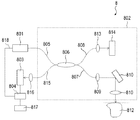
図5(a)に、一般的なMEMS−VCSELの断面模式図を示す。
図5(a)のMEMS−VCSELは、GaAsをベースとした化合物半導体で構成されており、中心波長を1065nmに設定し、その付近で波長可変となるように設計されている。上部反射鏡600と下部反射鏡610の間に活性層620が配置された共振器構造が基板640上に配置されている。この共振器構造内、具体的には、上部反射鏡600と活性層620の間に、上部反射鏡600が駆動できるように空隙部630がある。上部および下部反射鏡には、多層膜で形成した分布ブラッグ反射鏡(DBR)を使用している。
上部反射鏡600と下部反射鏡610の間の光学厚さを共振器長と呼ぶ。上部反射鏡600を光軸方向に動かすことで空隙部630の長さを変え、共振器長を変えることができる。それに伴ってレーザ発振波長が変化する。なお、ここでいう光軸方向とは、上部反射鏡と下部反射鏡を結ぶ方向であり、基板の主面に垂直な方向である。図中では上下方向に相当する。
下部反射鏡610と空隙部630の間の活性層620を含む半導体層650を半導体共振器と呼び、その光学厚さを半導体共振器長と呼ぶこととする。つまり、半導体共振器長は、下部反射鏡610と半導体層650との界面と、空隙部630と半導体層650との界面と、の間の光学的距離のことである。なお、共振器全体の共振器長は、半導体共振器長に空隙部の光学厚さを加えた長さとなる。
FIG. 5A shows a schematic cross-sectional view of a general MEMS-VCSEL.
The MEMS-VCSEL shown in FIG. 5A is made of a compound semiconductor based on GaAs, is set to have a central wavelength of 1065 nm, and is designed to be tunable in the vicinity thereof. A resonator structure in which an
The optical thickness between the upper reflecting
The
図6に、図5(a)に示したMEMS−VCSEL構造の空隙部の長さ(エアギャップ長)とレーザ発振波長の関係を計算した結果を示す。ここでは、中心波長をλとした場合に半導体共振器長が2λ、3λ、4λに相当する3種類の構造について計算した。
この計算結果から、半導体共振器長が長くなるほどグラフの傾きが小さくなることがわかる。グラフの傾きは、空隙部の長さ(dair)の変化に対するレーザ発振波長(λ)の変化(∂λ/∂dair)を表しており、これを波長チューニング効率と呼ぶ。
FIG. 6 shows the calculation results of the relationship between the length (air gap length) of the air gap of the MEMS-VCSEL structure shown in FIG. 5A and the laser oscillation wavelength. Here, when the central wavelength is λ, calculation was made for three types of structures in which the semiconductor resonator lengths correspond to 2λ, 3λ, and 4λ.
From this calculation result, it can be understood that the slope of the graph becomes smaller as the semiconductor resonator length becomes longer. The slope of the graph indicates a change in the lasing wavelength (λ) (∂λ / ∂d air ) with respect to a change in length of the gap portion (d air), referred to as wavelength tuning efficiency.
波長チューニング効率が大きいことはMEMS−VCSELにおいて以下の点で有利となる。
波長チューニング効率が大きいほど、同程度の発振波長変化をさせるのに必要な反射鏡の変位量を小さくすることができるので、反射鏡の機械的駆動のために必要な電圧などを下げることが可能になる。あるいは同程度の電圧で反射鏡を駆動する場合でも、ばね定数が大きく共振周波数が大きい構造を採用することが可能となるので、高速波長掃引に有利となる。
The large wavelength tuning efficiency is advantageous in the MEMS-VCSEL in the following points.
As the wavelength tuning efficiency is higher, the amount of displacement of the reflecting mirror required to cause the same degree of oscillation wavelength change can be made smaller, so it is possible to lower the voltage etc. required for the mechanical drive of the reflecting mirror. become. Alternatively, even when the reflecting mirror is driven with the same voltage, it is possible to adopt a structure having a large spring constant and a large resonance frequency, which is advantageous for high-speed wavelength sweeping.
また、波長チューニング効率を大きくすることは縦モード間隔を広げることにもつながる。縦モード間隔が狭い場合、モードホップによってレーザ発振波長が不連続的に跳んでしまったり、複数波長で同時に発振してしまったりして、シングルモードでの波長可変幅を制限する要因となる。縦モード間隔を広げることで、この制限を解消することが可能となる。 In addition, increasing the wavelength tuning efficiency leads to extending the longitudinal mode interval. When the longitudinal mode interval is narrow, the laser oscillation wavelength jumps discontinuously due to the mode hop, or oscillation occurs simultaneously at a plurality of wavelengths, which is a factor that limits the wavelength variable width in the single mode. This limitation can be eliminated by increasing the longitudinal mode interval.
波長チューニング効率が縦モード間隔に与える影響について、図7に示した計算結果を用いて説明する。
図7(a)と(b)は、共振器構造の異なる2種類のMEMS−VCSEL構造についての計算結果である。どちらも中心波長1065nm付近で波長可変となるように設計したMEMS−VCSELであるが、共振器構造の違いにより波長チューニング効率が異なっている。
図7(a)の中心波長付近での波長チューニング効率は約0.015であり、隣の次数の縦モードとの波長間隔は約25nmとなっている。一方、図7(b)の中心波長付近での波長チューニング効率は約0.12であり、隣の次数の縦モードとの波長間隔は約60nmとなっている。
このように、波長チューニング効率が大きい方が縦モード間隔も広がる傾向にあることが確認できる。
The influence of wavelength tuning efficiency on the longitudinal mode spacing will be described using the calculation results shown in FIG.
FIGS. 7A and 7B show calculation results of two types of MEMS-VCSEL structures having different resonator structures. Both are MEMS-VCSELs designed to be tunable at around the central wavelength of 1065 nm, but the wavelength tuning efficiency is different due to the difference in the resonator structure.
The wavelength tuning efficiency in the vicinity of the center wavelength in FIG. 7A is about 0.015, and the wavelength interval with the longitudinal mode of the next order is about 25 nm. On the other hand, the wavelength tuning efficiency in the vicinity of the central wavelength in FIG. 7B is about 0.12, and the wavelength interval to the longitudinal mode of the next order is about 60 nm.
Thus, it can be confirmed that the longitudinal mode interval tends to increase as the wavelength tuning efficiency increases.
図6に示した計算結果を用いて説明したように、波長チューニング効率の大きさは半導体共振器長に依存することが知られている。波長チューニング効率を大きくするためには半導体共振器長を短くすることが有効であるが、現実的には限界がある。
特に、電流注入によってレーザ発振する構造の場合は電流の拡散や狭窄のための層を設ける必要があるため、光励起によってレーザ発振する構造に比べて半導体共振器長を長くする必要があり、波長チューニング効率を大きくすることが難しい。
As described using the calculation results shown in FIG. 6, it is known that the magnitude of the wavelength tuning efficiency depends on the semiconductor resonator length. In order to increase the wavelength tuning efficiency, it is effective to shorten the semiconductor resonator length, but there is a practical limit.
In particular, in the case of a structure in which laser oscillation is performed by current injection, it is necessary to provide a layer for diffusion or narrowing of current, so it is necessary to make the semiconductor resonator length longer than the structure in which laser oscillation is performed by light excitation. It is difficult to increase the efficiency.
半導体共振器長を短くする以外の手段で波長チューニング効率を大きくする例として、空隙部と半導体共振器の界面に反射防止(AR)膜を設けた構成が一般に知られている。一方、空隙部と半導体共振器の界面に分布ブラッグ反射鏡(DBR)などの反射率を増大させるような構造を設けると、波長チューニング効率が小さくなることも一般に知られている(非特許文献1)。 As an example of increasing the wavelength tuning efficiency by means other than shortening the semiconductor resonator length, a configuration in which an anti-reflection (AR) film is provided on the interface between the air gap and the semiconductor resonator is generally known. On the other hand, it is generally known that the wavelength tuning efficiency is reduced if a structure such as a distributed Bragg reflector (DBR) is provided at the interface between the air gap and the semiconductor resonator to increase the reflectance (Non-Patent Document 1) ).
図5と図8を用いてこのことを説明する。
図5(a)〜(c)に、GaAsをベースとして波長1065nm付近で波長可変となるように構成したMEMS−VCSEL構造の断面模式図を示す。
図5(a)に示した構造は基本構造であり、空隙部630と半導体共振器650の界面に何も設けていない構造である。
図5(b)に示した構造は、図5(a)に示した構造の空隙部630と半導体共振器650の界面に反射防止(AR)膜660として酸化AlAs層を光学厚さ1/4波長だけ付加した構造である。
図5(c)に示した構造は、図5(a)に示した構造の空隙部630と半導体共振器650の界面にGaAs層と酸化AlAs層を光学厚さ1/4波長ずつ積層したDBR670を1ペア付加した構造である。
図5(a)〜(c)に示した構造全て、反射防止膜やDBRを除いた半導体共振器長は、中心波長1065nmを1.00λとした時に3.00λとなるように設計した。
This will be described using FIG. 5 and FIG.
5 (a) to 5 (c) are cross-sectional schematic views of a MEMS-VCSEL structure configured to be wavelength-tunable near a wavelength of 1065 nm based on GaAs.
The structure shown in FIG. 5A is a basic structure, in which nothing is provided at the interface between the
The structure shown in FIG. 5B has an optical thickness of 1⁄4 of an AlAs oxide layer as an anti-reflection (AR)
The structure shown in FIG. 5C is a
In all the structures shown in FIGS. 5A to 5C, the semiconductor resonator length excluding the antireflective film and the DBR is designed to be 3.00λ when the center wavelength 1065nm is 1.00λ.
なお、図5(a)〜(c)に示した各構造において、波長1065nmの光が半導体共振器650から空隙部630側に入射する場合の、半導体共振器650の空隙部630側の界面での反射率の計算値を以下に示す。図5(a)の構造では、半導体共振器650の空隙部630側の界面、つまり、半導体共振器650と空隙部630との界面の反射率は28.4%である。図5(b)の構造では、半導体共振器650の空隙部630側の界面、つまり、半導体共振器650と反射防止膜660との界面の反射率は0.1%である。図5(c)の構造では、半導体共振器650の空隙部630側の界面、つまり、半導体共振器650とDBR670(高反射構造)との界面の反射率は73.5%である。
In each of the structures shown in FIGS. 5A to 5C, when light having a wavelength of 1065 nm is incident from the
図8に、図5(a)〜(c)に示した各構造について、波長1065nm付近を基準に空隙部の長さ(エアギャップ長)の変化量とレーザ発振波長の関係を計算した結果を示す。
基本構造(図5(a)に相当)に対して、AR膜を付加した構造(図5(b)に相当)は波長チューニング効率が大きくなっており、DBRを付加した構造(図5(c)に相当)は逆に波長チューニング効率が小さくなっていることが確認される。
FIG. 8 shows the calculation results of the relationship between the variation of the air gap length (air gap length) and the laser oscillation wavelength based on the wavelength 1065 nm for each of the structures shown in FIGS. 5 (a) to 5 (c). Show.
In contrast to the basic structure (corresponding to FIG. 5 (a)), the structure (corresponding to FIG. 5 (b)) in which the AR film is added has a large wavelength tuning efficiency, and the structure in which DBR is added (FIG. On the contrary, it is confirmed that the wavelength tuning efficiency is reduced.
以上説明したように、MEMS−VCSELの共振器長をできるだけ短くしたり、空隙部と半導体共振器の界面にAR膜を設けたりすることで波長チューニング効率を向上できることが一般に知られてきた。
しかしながら、より高速かつ広帯域に波長を変えられるMEMS−VCSELを実現するためには、さらなる波長チューニング効率の向上が望まれている。
As described above, it has been generally known that the wavelength tuning efficiency can be improved by shortening the resonator length of the MEMS-VCSEL as much as possible or providing the AR film at the interface between the air gap and the semiconductor resonator.
However, in order to realize a MEMS-VCSEL whose wavelength can be changed to a higher speed and a wider band, further improvement in wavelength tuning efficiency is desired.
本発明を適用した構成では、従来の構成とは異なる半導体共振器長の選択と、空隙部と半導体共振器の界面の反射率増大とを組み合わせることで、従来の構成よりさらに波長チューニング効率を大きくすることが可能になる。
具体的には、半導体共振器長がλ/2×m+λ/4近傍となるように構成し、空隙部と半導体共振器の界面に高反射率構造を設けることで、上記の効果を得ることができる。(mは1以上の整数、λは中心波長。以下同じ。)
ここで言う高反射率構造とは、半導体共振器を構成する主成分である半導体材料の屈折率と空隙部の屈折率の差によって界面で生じる光反射よりも反射率を大きくするように構成された構造のことである。例を挙げると、相対的に高屈折率の材料からなる高屈折率層と相対的に低屈折率の材料からなる低屈折率層が少なくとも1ペア積層された構造である。より好ましくは、DBRのように相対的に高屈折率の材料と低屈折率の材料が中心波長をλとした時に光学厚さλ/4の奇数倍となる厚さで交互に積層された多層膜構造である。
また、半導体共振器は、高反射率構造と下部反射鏡との間に配置された全ての半導体層の積層体である。
In the configuration to which the present invention is applied, the wavelength tuning efficiency is made larger than that of the conventional configuration by combining the selection of the semiconductor resonator length different from the conventional configuration and the increase in the reflectivity of the interface between the air gap and the semiconductor resonator. It will be possible to
Specifically, the above effect can be obtained by configuring the semiconductor resonator length to be in the vicinity of λ / 2 × m + λ / 4 and providing a high reflectance structure at the interface between the air gap and the semiconductor resonator. it can. (M is an integer of 1 or more, λ is the central wavelength, and so forth)
The high reflectance structure mentioned here is configured to make the reflectance larger than the light reflection generated at the interface due to the difference between the refractive index of the semiconductor material which is the main component of the semiconductor resonator and the refractive index of the air gap. Structure. An example is a structure in which at least one pair of a high refractive index layer made of a relatively high refractive index material and a low refractive index layer made of a relatively low refractive index material is laminated. More preferably, a multilayer in which a material having a relatively high refractive index and a material having a low refractive index, such as DBR, is alternately stacked at a thickness that is an odd multiple of the optical thickness λ / 4 when the central wavelength is λ. It is a membrane structure.
The semiconductor resonator is a laminate of all the semiconductor layers disposed between the high reflectance structure and the lower reflecting mirror.
図1に、本発明を適用したMEMS−VCSELの一例を示して説明する。
上から順に上部反射鏡100、空隙部130、高反射率構造170、活性層120を含む半導体共振器150、下部反射鏡110、基板140が配置されている。半導体共振器150の光学厚さを半導体共振器長と呼ぶ。つまり、半導体共振器長は、高反射率構造170と半導体共振器150との界面と、半導体共振器150と下部反射鏡110との界面と、の間の光学的距離のことである。
本発明を適用した構成において、中心波長をλとした場合に半導体共振器長はλ/2×m+λ/4となるように構成されている。
本発明において、MEMS−VCSELは、不図示の電極により活性層120に電流が注入されて発光する電流注入型であってもよいし、不図示の外部光源により活性層120に励起光が照射される光励起型であってもよい。
また、上部反射鏡100は、不図示の電極の間に電圧が印加されることで静電気力によりMEMS−VCSELの厚さ方向に駆動される。
An example of a MEMS-VCSEL to which the present invention is applied is shown and described in FIG.
The upper reflecting
In the configuration to which the present invention is applied, when the central wavelength is λ, the semiconductor resonator length is configured to be λ / 2 × m + λ / 4.
In the present invention, the MEMS-VCSEL may be a current injection type in which current is injected into the
In addition, the upper reflecting
なお、本明細書中での半導体共振器長の表記は、半導体共振器の上部および下部の界面での光反射時の位相変化が無い、自由端反射の場合に換算している。換算とは、半導体共振器の上部および下部の界面での光反射時の位相変化がある場合には、半導体共振器長の光学厚さを、その位相変化分を考慮した光学厚さにすることである。具体的な換算の方法は、例えば非特許文献1の第3パラグラフなどに記載されている。
反射時の位相変化がある場合は、それに応じて実効的な光路長が伸び縮みすることとなり、実際の半導体共振器長を調整する必要がある。例えば、反射時の位相変化がπである固定端反射の場合、自由端反射の場合に比べてλ/2分だけ実効的な光路長がずれる。共振器の往復でλ/2分の光路長差を付けるためにはλ/4分だけ共振器長を変える必要がある。
例えば半導体共振器の上部または下部の界面のどちらか一方が固定端反射となる場合には、本発明に適した半導体共振器長はλ/2×m+λ/4からλ/4を引いた値(またはλ/4を足した値)であり、λ/2×mとなる。
本明細書中では、特に言及しないかぎり半導体共振器の上部および下部の界面での光反射は自由端反射となるような構成になっているものとする。
Incidentally, the notation of the semiconductor resonator length in the present specification is converted to the case of free end reflection where there is no phase change at the time of light reflection at the upper and lower interfaces of the semiconductor resonator. The conversion means that if there is a phase change at the time of light reflection at the upper and lower interfaces of the semiconductor resonator, the optical thickness of the semiconductor resonator length should be an optical thickness considering the phase change. It is. A specific conversion method is described, for example, in the third paragraph of Non-Patent Document 1 and the like.
If there is a phase change at the time of reflection, the effective optical path length will expand and contract accordingly, and the actual semiconductor resonator length needs to be adjusted. For example, in the case of fixed end reflection in which the phase change upon reflection is π, the effective optical path length deviates by λ / 2 as compared with the case of free end reflection. In order to make an optical path length difference of λ / 2 in the round trip of the resonator, it is necessary to change the resonator length by λ / 4.
For example, when one of the upper and lower interfaces of the semiconductor resonator is fixed end reflection, the semiconductor resonator length suitable for the present invention is a value obtained by subtracting λ / 4 from λ / 2 × m + λ / 4 Or λ / 4) to obtain λ / 2 × m.
In this specification, light reflection at the upper and lower interfaces of the semiconductor resonator is assumed to be free-end reflection unless otherwise stated.
なお、一般的に、屈折率が大きい材料からなる層から屈折率が小さい材料からなる層へ光が入射する場合は、その2つの層の界面での光反射は自由端反射となる。一方、屈折率が小さい材料からなる層から屈折率が大きい材料からなる層へ光が入射する場合は固定端反射となる。
また、多層膜の場合は各界面からの反射光が合波されたものとなるため、明確な自由端や固定端とはならない場合がある。DBRの場合、基本的にはDBRの活性層に最も近い層の屈折率がその層と接する入射側の層の媒質に比べて屈折率が大きい場合には、固定端反射になる。一方、DBRの活性層に最も近い層の屈折率がその層と接する入射側の層の媒質に比べて屈折率が小さい場合には、自由端反射になる。しかし、DBRの各層の光学厚さがλ/4からずれるにつれて少しずつ固定端反射や自由端反射と言えなくなる。また、膜厚変調DBRのような、高屈折率層がλ/4より厚く低屈折率層がλ/4より薄いDBRなどでは、中心波長でも自由端反射や固定端反射にならない。
この点を踏まえて、本発明のMEMS−VCSELでは、自由端反射の場合に換算して、中心波長をλとした場合に半導体共振器長がλ/2×m+λ/4となるように構成されている。
In general, when light is incident from a layer made of a material having a large refractive index to a layer made of a material having a small refractive index, light reflection at the interface between the two layers is free end reflection. On the other hand, when light is incident from a layer made of a material having a small refractive index to a layer made of a material having a large refractive index, fixed end reflection is obtained.
Further, in the case of a multilayer film, the reflected light from each interface is combined, so that it may not be a clear free end or a fixed end. In the case of DBR, basically, when the refractive index of the layer closest to the DBR active layer is larger than the refractive index of the medium on the incident side in contact with that layer, fixed end reflection is obtained. On the other hand, when the refractive index of the layer closest to the DBR active layer is smaller than the refractive index of the medium on the incident side in contact with that layer, free-end reflection occurs. However, as the optical thickness of each layer of the DBR deviates from λ / 4, it can not be said as fixed end reflection or free end reflection. Further, in a DBR or the like in which the high refractive index layer is thicker than λ / 4 and the low refractive index layer is thinner than λ / 4 like the film thickness modulation DBR, free end reflection or fixed end reflection does not occur even at the center wavelength.
Based on this point, in the MEMS-VCSEL according to the present invention, the semiconductor resonator length is configured to be λ / 2 × m + λ / 4 when the central wavelength is λ in terms of free end reflection. ing.
上部反射鏡100および下部反射鏡110には、多層膜で形成した分布ブラッグ反射鏡(DBR)を使用している。上部反射鏡100と下部反射鏡110に挟まれた領域が共振器となっており、光定在波が形成される。上部反射鏡100は光軸方向(図の上下方向)に可動となっており、空隙部130の長さ(以下、エアギャップ長と呼ぶ)が変わることで共振器長が変化し、レーザ発振波長が変わる。
For the upper reflecting
図2に、図1に示した構造および比較用の構造について、エアギャップ長の変化量とレーザ発振波長の関係を計算した結果を示す。
図5や図8を用いて説明した時と同様、基本構造は空隙部と半導体共振器の界面に何も設けていない構造である。AR膜付加は空隙部と半導体共振器の界面にAR膜を形成した構造である。DBR付加は空隙部と半導体共振器の界面に高反射率構造としてDBRを形成した構造である。DBR付加が本発明を適用した構成であり、基本構造とAR膜付加が比較用の構成である。
なお、AR膜やDBRを除いた半導体共振器長は、中心波長1065nmを1.00λとした時に3.25λとなるように設計した。
FIG. 2 shows the result of calculating the relationship between the amount of change in the air gap length and the laser oscillation wavelength for the structure shown in FIG. 1 and the structure for comparison.
As in the case described with reference to FIGS. 5 and 8, the basic structure is a structure in which nothing is provided at the interface between the air gap and the semiconductor resonator. The AR film addition is a structure in which the AR film is formed at the interface between the air gap and the semiconductor resonator. The DBR addition is a structure in which a DBR is formed as a high reflectance structure at the interface between the air gap and the semiconductor resonator. The DBR addition is the configuration to which the present invention is applied, and the basic structure and the AR film addition are the configurations for comparison.
The semiconductor resonator length excluding the AR film and the DBR was designed to be 3.25 λ when the central wavelength 1065 nm was 1.00 λ.
図2に示した計算結果は、先ほど図8を用いて説明した比較例の構造の計算結果と比較すると大きな違いが見られる。
その違いを明瞭にするために、図2と図8に示した計算結果から各構造の波長チューニング効率を読み取って、大きい順に並べた表を表1に示す。
The calculation results shown in FIG. 2 are significantly different from the calculation results of the structure of the comparative example described above with reference to FIG.
In order to clarify the difference, the wavelength tuning efficiency of each structure is read from the calculation results shown in FIG. 2 and FIG. 8, and a table arranged in descending order is shown in Table 1.

この表から読み取れることは以下のことである。
まず、半導体共振器長を3.00λから3.25λにすることで、共振器長が長くなるにも関わらず基本構造の波長チューニング効率が向上する。
基本構造にAR膜を付加した構造について、従来の半導体共振器長3.00λの場合は波長チューニング効率が大きくなるが、本発明を適用した半導体共振器長3.25λの構造の場合では逆に波長チューニング効率が小さくなる結果が得られた。
一方、基本構造にDBRを付加した構造について、従来の半導体共振器長3.00λの場合は波長チューニング効率が小さくなるが、本発明を適用した半導体共振器長3.25λの構造の場合では逆に波長チューニング効率が大きくなる結果が得られた。
この結果は、半導体共振器長によって波長チューニング効率が変化し、空隙部と半導体共振器の界面の反射率によってその変化量が拡大されたり縮小されたりするということであると理解できる。
The following can be read from this table.
First, by setting the semiconductor resonator length from 3.00λ to 3.25λ, the wavelength tuning efficiency of the basic structure is improved despite the increase in the resonator length.
In the structure in which the AR film is added to the basic structure, the wavelength tuning efficiency is increased in the case of the conventional semiconductor resonator length of 3.00λ, but in the case of the structure of the semiconductor resonator length of 3.25λ to which the present invention is applied. The result is obtained that the wavelength tuning efficiency is reduced.
On the other hand, in the structure in which DBR is added to the basic structure, the wavelength tuning efficiency decreases in the case of the conventional semiconductor resonator length of 3.00λ, but in the case of the structure of the semiconductor resonator length of 3.25λ to which the present invention is applied The result is that the wavelength tuning efficiency is increased.
It can be understood that the result is that the wavelength tuning efficiency changes with the length of the semiconductor resonator, and the amount of change is expanded or reduced by the reflectance of the interface between the air gap and the semiconductor resonator.
このことについて、図3を用いてより詳しく説明する。
図3に、様々な構造のMEMS−VCSELについて、中心波長1065nmにおける波長チューニング効率と半導体共振器長の関係を計算した結果を示す。
空隙部と半導体共振器の界面に何も設けない基本構造と、界面にDBRを1ペア、3ペア、5ペア設けた構造と、界面にAR膜を設けた構造の、中心波長1065nm付近における波長チューニング効率の半導体共振器長依存性を計算したものである。
図3を見ると、半導体共振器長がλ/4変わるごとに波長チューニング効率が増減を繰り返すことがわかる。また、細かい増減を繰り返しながら、全体的な傾向としては半導体共振器長が長くなるほど波長チューニング効率が下がることも見て取れる。
ここで、AR膜を設けた構造では半導体共振器長の変化に対する波長チューニング効率の増減の幅が小さくなっている。
一方、DBRを設けた構造では半導体共振器長の変化に対する波長チューニング効率の増減の幅が大きくなっている。また、DBRのペア数が増えるにつれてさらに波長チューニング効率の増減の幅が大きくなる。
This will be described in more detail with reference to FIG.
FIG. 3 shows the result of calculating the relationship between the wavelength tuning efficiency at a central wavelength of 1065 nm and the semiconductor resonator length for MEMS-VCSELs of various structures.
A wavelength around the central wavelength of 1065 nm of the basic structure in which nothing is provided at the interface between the gap and the semiconductor resonator, the structure in which 1 pair, 3 pairs, 5 pairs of DBRs are provided in the interface, and the structure in which the AR film is provided in the interface The semiconductor resonator length dependency of tuning efficiency is calculated.
It can be seen from FIG. 3 that the wavelength tuning efficiency repeatedly increases and decreases each time the semiconductor resonator length changes by λ / 4. In addition, it can also be seen that the wavelength tuning efficiency decreases as the semiconductor resonator length increases as the overall tendency while repeating the fine increase and decrease.
Here, in the structure provided with the AR film, the range of increase and decrease of the wavelength tuning efficiency with respect to the change of the semiconductor resonator length is small.
On the other hand, in the structure provided with the DBR, the range of increase and decrease of the wavelength tuning efficiency with respect to the change of the semiconductor resonator length is large. Further, as the number of DBR pairs increases, the range of increase and decrease in wavelength tuning efficiency further increases.
従来、空隙部と半導体共振器の界面にAR膜を付加することで波長チューニング効率が向上すると言われてきたが、これまでに検討されたのは半導体共振器長がλ/2×mの場合に限られていた。
図3を用いて説明したように、λ/2×m+λ/4の半導体共振器長にAR膜を付加すると、逆に波長チューニング効率が悪化してしまうということが本発明者らの検討により判明した。
この結果について定性的な考察を試みる。
AR膜などの反射率を低減する構造は、半導体共振器長の違いに対して鈍感にさせる効果を持つと理解できる。それにより、どのような半導体共振器長であっても、AR膜を形成しない場合の波長チューニング効率の大きい半導体共振器長と小さい半導体共振器長の中間的な特性が得られる。
つまり、もともと波長チューニング効率の小さい半導体共振器長(λ/2×m)の場合にはAR膜を付加することで波長チューニング効率を大きくすることができる。一方、もともと波長チューニング効率の大きい半導体共振器長(λ/2×m+λ/4)の場合はAR膜を付加することで波長チューニング効率が小さくなってしまう。
逆に、DBRなどの反射率を増大させる構造は半導体共振器長の違いに対して敏感にさせる効果を持つと理解できる。つまり、もともと波長チューニング効率の小さい半導体共振器長(λ/2×m)の場合にはDBRを付加することで波長チューニング効率がさらに小さくなる。一方、もともと波長チューニング効率の大きい半導体共振器長(λ/2×m+λ/4)の場合はDBRを付加することで波長チューニング効率がさらに大きくなる。
結果として、波長チューニング効率を大きくするという観点では、λ/2×m+λ/4の半導体共振器長にDBRなどの高反射率構造を付加した構造が最適となる。
Conventionally, it has been said that the wavelength tuning efficiency is improved by adding an AR film to the interface between the air gap and the semiconductor resonator, but what has been studied so far is the case where the semiconductor resonator length is λ / 2 × m It was limited to
As described with reference to FIG. 3, the inventors found that the wavelength tuning efficiency is deteriorated when the AR film is added to the semiconductor resonator length of λ / 2 × m + λ / 4. did.
We will try to consider qualitatively about this result.
It can be understood that the structure for reducing the reflectance, such as the AR film, has the effect of making it insensitive to differences in semiconductor resonator length. Thus, regardless of the semiconductor resonator length, it is possible to obtain an intermediate characteristic between the semiconductor resonator length with high wavelength tuning efficiency and the small semiconductor resonator length when the AR film is not formed.
That is, in the case of a semiconductor resonator length (λ / 2 × m) originally having a small wavelength tuning efficiency, the wavelength tuning efficiency can be increased by adding the AR film. On the other hand, in the case of the semiconductor resonator length (λ / 2 × m + λ / 4) originally having a large wavelength tuning efficiency, the wavelength tuning efficiency is reduced by adding the AR film.
Conversely, it can be understood that a structure that increases the reflectance, such as DBR, has the effect of making it sensitive to differences in semiconductor resonator length. That is, in the case of the semiconductor resonator length (λ / 2 × m) originally having a small wavelength tuning efficiency, the wavelength tuning efficiency is further reduced by adding the DBR. On the other hand, in the case of the semiconductor resonator length (λ / 2 × m + λ / 4) originally having a large wavelength tuning efficiency, the wavelength tuning efficiency is further increased by adding the DBR.
As a result, from the viewpoint of increasing the wavelength tuning efficiency, a structure in which a high reflectance structure such as DBR is added to the semiconductor resonator length of λ / 2 × m + λ / 4 is optimum.
本発明を適用した構成において、半導体共振器長は厳密にλ/2×m+λ/4に一致していなくても、ある程度の範囲内であれば本発明の効果を得ることができる。λ/2×mよりもλ/2×m+λ/4に近い値であればよい。つまり、半導体共振器長をLとすると、
λ/2×m+λ/8 < L < λ/2×m+3λ/8(mは1以上の整数、λはレーザ発振の中心波長)
を満たす範囲であれば本発明の効果が得られる。
さらに、
λ/2×m+7λ/40 ≦ L ≦ λ/2×m+13λ/40
を満たす範囲であれば、基本構造よりも波長チューニング効率が向上するため好ましい。
さらに、
λ/2×m+3λ/16 ≦ L ≦ λ/2×m+5λ/16
を満たす範囲であれば、よりλ/2×m+λ/4に近い範囲であり、好適である。
In the configuration to which the present invention is applied, even if the semiconductor resonator length does not strictly coincide with λ / 2 × m + λ / 4, the effect of the present invention can be obtained within a certain range. It may be a value closer to λ / 2 × m + λ / 4 than λ / 2 × m. That is, when the semiconductor resonator length is L,
λ / 2 × m + λ / 8 <L <λ / 2 × m + 3λ / 8 (m is an integer of 1 or more, λ is the central wavelength of laser oscillation)
The effects of the present invention can be obtained as long as
further,
λ / 2 × m + 7λ / 40 ≦ L ≦ λ / 2 × m + 13λ / 40
If the range satisfies the above, it is preferable because the wavelength tuning efficiency is improved compared to the basic structure.
further,
λ / 2 × m + 3λ / 16 ≦ L ≦ λ / 2 × m + 5λ / 16
If the range is satisfied, the range is closer to λ / 2 × m + λ / 4, which is preferable.
本発明を適用した構成において、上部反射鏡および下部反射鏡は、レーザ発振に足る反射率を得られるものであれば特に制限はない。例えば、誘電体や半導体多層膜で構成されたDBR、金属膜、回折格子などを使用することができる。 In the configuration to which the present invention is applied, the upper reflecting mirror and the lower reflecting mirror are not particularly limited as long as they can obtain reflectivity sufficient for laser oscillation. For example, a DBR composed of a dielectric or a semiconductor multilayer film, a metal film, a diffraction grating or the like can be used.
本発明を適用した構成において、空隙部と半導体共振器の界面に設けた高反射率構造は、反射率を増大させるものであればよい。例えば、誘電体や半導体多層膜で構成されたDBR、金属膜、回折格子などを使用することができる。
この中でも、半導体多層膜で構成されたDBR(いわゆる半導体DBR)を使用する場合は、次のような理由から、特に好ましい。すなわち、結晶成長により半導体共振器の後に続けて一括で形成できるという製造上の利点や、導電性を持っているため電流を拡散させることができ電流注入の均一化に役立つといった利点が挙げられる。
また、誘電体多層膜で構成されたDBR(いわゆる誘電体DBR)を使用する場合は、導電性を持たせることができないという点で半導体DBRに劣るが、半導体多層膜より大きな屈折率差を得ることができ、容易に高い反射率を得やすいという点で優れている。そのため、用途によっては半導体DBRより誘電体DBRを用いる方が好ましい場合もある。
In the configuration to which the present invention is applied, the high reflectance structure provided at the interface between the air gap portion and the semiconductor resonator may be one that increases the reflectance. For example, a DBR composed of a dielectric or a semiconductor multilayer film, a metal film, a diffraction grating or the like can be used.
Among these, when using a DBR (so-called semiconductor DBR) composed of a semiconductor multilayer film, it is particularly preferable for the following reasons. That is, there are manufacturing advantages such as being able to be formed collectively at once after the semiconductor resonator by crystal growth, and being advantageous in that it has conductivity and can spread current and help equalize current injection.
In addition, when using DBRs (so-called dielectric DBRs) composed of dielectric multi-layered films, although they are inferior to semiconductor DBRs in that they can not have conductivity, they have a larger difference in refractive index than semiconductor multi-layered films. It is excellent in that it is easy to obtain high reflectance. Therefore, it may be preferable to use a dielectric DBR rather than a semiconductor DBR depending on the application.
本発明を適用した構成において、活性層は一般的な面発光レーザに使用されているものを使用することができる。活性層を構成する材料の組成や層厚などはレーザ発振させたい波長に応じて適宜選択することができる。 In the configuration to which the present invention is applied, the active layer can be one used in a general surface emitting laser. The composition, layer thickness, and the like of the material constituting the active layer can be appropriately selected according to the wavelength at which laser oscillation is desired.
本発明を適用した構成において、上部反射鏡を光軸方向に沿って上下に変位させる手段は、MEMS分野で一般的に使用されている技術を利用することができる。例えば静電、圧電、熱、電磁、流体圧などを利用することができる。 In the configuration to which the present invention is applied, the means for vertically displacing the upper reflecting mirror along the optical axis direction can utilize a technique generally used in the field of MEMS. For example, electrostatic, piezoelectric, heat, electromagnetic, fluid pressure etc. can be used.
本発明を適用した構成において、空隙部には気体や液体を充填することができ、真空にすることもできる。ここで言う真空とは、気圧が標準大気圧より低い負圧の状態を指すこととする。本明細書中では、空隙部には空気が充填されているものと想定し、屈折率は1であるとして計算を行った。 In the configuration to which the present invention is applied, the void portion can be filled with gas or liquid, and can be vacuum. The term "vacuum" as used herein refers to a negative pressure where the pressure is lower than the standard atmospheric pressure. In the present specification, calculation is performed on the assumption that the void is filled with air and the refractive index is 1.
本発明を適用した面発光レーザは、光励起または電流注入でレーザ発振させることができる。電流注入を行う場合は電極を設ける必要があるが、本明細書および図面では記載を簡潔にするために電極は省略している。 The surface emitting laser to which the present invention is applied can be oscillated by light excitation or current injection. Although it is necessary to provide an electrode when performing current injection, the electrode is omitted in the present specification and the drawings for the sake of simplicity.
また、本発明を適用した面発光レーザを同一平面上に複数配列してアレイ光源として使用してもよい。 In addition, a plurality of surface emitting lasers to which the present invention is applied may be arranged on the same plane and used as an array light source.
(実施形態2)
本実施形態では、実施形態1で示した面発光レーザを備えた光源装置の応用例について説明する。波長可変型の光源装置は、光通信用光源や光計測用光源として利用することができる。また、この光源装置は、非侵襲、非破壊で測定対象物の内部の情報を取得する情報取得装置の光源装置として利用することができる。以下では、本実施形態の光源装置を用いた情報取得装置の一例として、光干渉断層計(以下、OCT装置という)について図4を用いて説明する。
図4は、本実施形態に係るOCT装置8を示す模式図である。OCT装置8は、光源装置801、干渉光学系802、光検出部803、測定対象物の内部情報を取得する情報取得部804、を少なくとも有する。光源装置801として、実施形態1の面発光レーザを用いることができる。また、図示していないが、情報取得部804はフーリエ変換器を有する。ここで、情報取得部804がフーリエ変換器を有するとは、情報取得部804が入力されたデータに対してフーリエ変換する機能を有していれば形態は特に限定されない。一例は、情報取得部804が演算部を有し、この演算部がフーリエ変換する機能を有する場合である。具体的には、演算部がCPUを有するコンピュータであり、このコンピュータが、フーリエ変換機能を有するアプリケーションを実行する場合である。他の例は、情報取得部804がフーリエ変換機能を有するフーリエ変換回路を有する場合である。
Second Embodiment
In this embodiment, an application example of the light source device provided with the surface emitting laser shown in the first embodiment will be described. The variable-wavelength light source device can be used as a light source for optical communication or a light source for light measurement. Further, this light source device can be used as a light source device of an information acquisition device that acquires information inside the measurement object noninvasively and nondestructively. Hereinafter, an optical coherence tomography (hereinafter referred to as an OCT apparatus) will be described using FIG. 4 as an example of the information acquisition apparatus using the light source device of the present embodiment.
FIG. 4 is a schematic view showing an
光源装置801から出た光は干渉光学系802を経て測定対象の物体812の情報を有する干渉光となって出力される。干渉光は光検出部803において受光される。なお光検出部803は差動検出型でも良いし単純な強度モニタ型でも良い。受光された干渉光の強度の時間波形の情報は光検出部803から情報取得部804に送られる。情報取得部804では、受光された干渉光の強度の時間波形のピーク値を取得してフーリエ変換をし、物体812の情報(例えば断層像の情報)を取得する。なお、ここで挙げた光源装置801、干渉光学系802、光検出部803、情報取得部804を任意に設けることができる。
以下、光源装置801から光が照射されてから、測定対象の物体の内部の情報を得るまでについて詳細に説明する。光源装置801から出た光は、ファイバ805を通って、カップラ806に入り、照射光用のファイバ807を通る照射光と、参照光用のファイバ808を通る参照光とに分岐される。カップラ806は、光源の波長帯域でシングルモード動作のもので構成し、各種ファイバカップラは3dBカップラで構成することができる。照射光はコリメーター809を通って平行光になり、ミラー810で反射される。ミラー810で反射された光はレンズ811を通って物体812に照射され、物体812の奥行き方向の各層から反射される。
The light emitted from the
Hereinafter, after light is irradiated from the
一方、参照光はコリメーター813を通ってミラー814で反射される。カップラ806では、物体812からの反射光とミラー814からの反射光による干渉光が発生する。干渉した光はファイバ815を通り、コリメーター816を通って集光され、光検出部803で受光される。光検出部803で受光された干渉光の強度の情報は電圧などの電気的な情報に変換されて、情報取得部804に送られる。情報取得部804では、干渉光の強度のデータを処理、具体的にはフーリエ変換し断層像の情報を得る。このフーリエ変換する干渉光の強度のデータは通常、等波数間隔にサンプリングされたデータであるが、等波長間隔にサンプリングされたデータを用いることも可能である。
Meanwhile, the reference light passes through the
得られた断層像の情報は、情報取得部804から画像表示部817に送って画像として表示させてもよい。なお、ミラー810を照射光の入射する方向と垂直な平面内で走査することで、測定対象の物体812の3次元の断層像を得ることができる。また、光源装置801の制御は、情報取得部804が電気回路818を介して行ってもよい。また図示しないが、光源装置801から出る光の強度を逐次モニタリングし、そのデータを干渉光の強度の信号の振幅補正に用いてもよい。
Information on the obtained tomographic image may be sent from the
OCT装置は、眼科、歯科、皮膚科等の分野において、動物や人のような生体内の断層像を取得する際に有用である。生体の断層像に関する情報とは、生体の断層像のみならず、断層像を得るために必要な数値データをも含む。特に、測定対象を人体の眼底や歯、血管とし、それらの断層像に関する情報を取得することに用いられることが好適である。 The OCT apparatus is useful in obtaining a tomogram in a living body such as an animal or a person in the fields of ophthalmology, dentistry, dermatology and the like. The information on the tomogram of the living body includes not only the tomogram of the living body but also numerical data necessary for obtaining the tomogram. In particular, it is preferable that the measurement target be a fundus, teeth, or blood vessels of a human body, and that it be used to acquire information on their tomograms.
以下に、本発明の実施例について説明する。なお、本発明は以下に説明する実施例の構成に限定されるものではない。例えば、材料の種類や組成、形状や大きさは本発明の範囲内で適宜変更できる。
以下の実施例では、レーザ発振波長として1060nm付近のものを示したが、適切な材料・構造の選択により、任意の波長での動作も可能である。
Hereinafter, examples of the present invention will be described. The present invention is not limited to the configurations of the embodiments described below. For example, the type, composition, shape and size of the material can be suitably changed within the scope of the present invention.
In the following embodiments, the laser oscillation wavelength is around 1060 nm. However, operation at an arbitrary wavelength is also possible by selecting an appropriate material and structure.
[実施例1]
実施例1として、本発明を適用したVCSELについて、図1を用いて説明する。図1は、本実施例におけるVCSELの層構造を示す断面模式図である。
本実施例におけるVCSELは、GaAsをベースとした化合物半導体で構成されており、中心波長1060nm付近で波長掃引できるように設計されたものである。
上から順に上部反射鏡100、空隙部130、高反射率構造170、活性層120を含む半導体共振器150、下部反射鏡110、GaAs基板140が配置されている。
上部反射鏡100は、Al0.4Ga0.6AsとAl0.9Ga0.1Asを交互に36.5ペア積層したDBRで構成されている。
上部反射鏡100は電圧印加による静電力で上下方向の位置を変えることができるようになっている。図中では電圧印加用の電極は省略している。
空隙部130には空気が充填されており、空隙部130の長さ(エアギャップ長)は1600nm付近で可変となっている。高反射率構造170は、上部反射鏡100と同様にAl0.4Ga0.6AsとAl0.9Ga0.1Asを交互に5ペア積層したDBRで構成されている。
活性層120はGaInAsからなる量子井戸層とGaAsPからなる障壁層を3周期積層した多重量子井戸構造で構成されている。
活性層120は電流注入により発光する。なお、図中では電流注入のための電極は省略している。
半導体共振器長は、中心波長1060nmを1.00λとしたときに1.75λ付近に相当するように構成されている。
下部反射鏡110はGaAsとAlAsを交互に30ペア積層した上にAl0.4Ga0.6AsとAl0.9Ga0.1Asを交互に5ペア積層したDBRで構成されている。
Example 1
As Example 1, a VCSEL to which the present invention is applied will be described with reference to FIG. FIG. 1 is a schematic cross-sectional view showing the layer structure of the VCSEL in the present embodiment.
The VCSEL in the present embodiment is made of a compound semiconductor based on GaAs, and designed to be capable of wavelength sweeping around a central wavelength of 1060 nm.
The upper reflecting
The upper reflecting
The upper reflecting
The
The
The
The semiconductor resonator length is configured to correspond to around 1.75 λ when the
The lower reflecting
本実施例の空隙部130は、エピタキシャル成長と選択ウエットエッチングを用いて形成した。その手順の概要を説明する。
エピタキシャル成長を行う際、空隙部に相当する部分をGaAsの犠牲層として成膜しておく。
水とクエン酸と過酸化水素水との混合液をエッチャントとして用いることで、AlGaAsのAl組成に応じた選択エッチングが可能である。本実施例では、水およびクエン酸(重量比1:1)を混ぜ合わせたクエン酸溶液と、濃度30%の過酸化水素水とを4:1の割合(体積比)で混ぜたものをエッチャントとして用いた。このエッチャントでGaAsとAl0.7Ga0.3Asの選択エッチングが可能であり、GaAs犠牲層だけを除去することで空隙部を形成することができる。
The void 130 in this example was formed using epitaxial growth and selective wet etching. An outline of the procedure is described.
At the time of epitaxial growth, a portion corresponding to the void portion is formed as a sacrificial layer of GaAs.
By using a mixture of water, citric acid and hydrogen peroxide as an etchant, selective etching according to the Al composition of AlGaAs is possible. In this embodiment, the etchant is a mixture of a citric acid solution in which water and citric acid (1: 1 by weight) are mixed, and a hydrogen peroxide solution having a concentration of 30% in a ratio (volume ratio) of 4: 1. Used as Selective etching of GaAs and Al 0.7 Ga 0.3 As is possible with this etchant, and a void can be formed by removing only the GaAs sacrificial layer.
波長1060nmの光に対する高反射率構造170の反射率は約60%であり、高反射率構造を設けない場合の空隙部と半導体共振器の界面における反射率(約28%)に比べて大きい。それにより、波長チューニング効率を大きくすることができる。
計算によると、高反射率構造170を設けない場合の波長チューニング効率は0.246であるが、本実施例のように高反射率構造170を設けることで波長チューニング効率を0.262に改善できる。
このように、本発明を適用した構成では、従来よりも優れた波長チューニング効率を有する波長可変型の面発光レーザが得られる。
The reflectance of the
According to the calculation, the wavelength tuning efficiency without the
As described above, in the configuration to which the present invention is applied, it is possible to obtain a variable-wavelength surface emitting laser having wavelength tuning efficiency superior to that of the prior art.
100:上部反射鏡
110:下部反射鏡
120:活性層
130:空隙部
140:基板
150:半導体共振器
170:高反射率構造
100: upper reflector 110: lower reflector 120: active layer 130: air gap portion 140: substrate 150: semiconductor resonator 170: high reflectance structure
Claims (11)
前記空隙部と前記半導体共振器の間に高反射率構造を備え、
前記高反射率構造と前記半導体共振器との界面と前記半導体共振器と前記下部反射鏡との界面との間の光学的距離である前記半導体共振器の光学厚さLが、前記半導体共振器の該上部および下部の界面での光反射時の位相変化が無い場合に換算して、
λ/2×m+λ/8 < L < λ/2×m+3λ/8 (mは1以上の整数、λはレーザ発振の中心波長)
であり、
前記高反射率構造が、相対的に高屈折率の材料からなる高屈折率層と相対的に低屈折率の材料からなる低屈折率層が少なくとも1ペア積層された構造であることを特徴とする面発光レーザ。 A surface provided with an upper reflecting mirror, a semiconductor resonator including an active layer, and a lower reflecting mirror in this order, a gap is formed between the upper reflecting mirror and the semiconductor layer, and the resonator length is variable. A light emitting laser,
A high reflectance structure is provided between the air gap and the semiconductor resonator,
The optical thickness L of the semiconductor resonator, which is the optical distance between the interface between the high reflectance structure and the semiconductor resonator and the interface between the semiconductor resonator and the lower reflection mirror, is the semiconductor resonator. in terms of when there is no phase change upon reflection of light at the top and bottom of the interface,
λ / 2 × m + λ / 8 <L <λ / 2 × m + 3λ / 8 (m is an integer of 1 or more, λ is the central wavelength of laser oscillation)
And
The high reflectance structure is a structure in which at least one pair of a high refractive index layer made of a material having a relatively high refractive index and a low refractive index layer made of a material having a relatively low refractive index are laminated. Surface emitting laser.
前記空隙部と前記半導体共振器の間に高反射率構造を備え、
前記高反射率構造と前記半導体共振器との界面または前記半導体共振器と前記下部反射鏡との界面のどちらか一方が固定端反射となり、
前記半導体共振器の該上部の界面と該下部の界面との間の光学的距離である前記半導体共振器の光学厚さLが、
λ/2×m−λ/8 < L < λ/2×m+λ/8 (mは1以上の整数、λはレーザ発振の中心波長)
であり、
前記高反射率構造が、相対的に高屈折率の材料からなる高屈折率層と相対的に低屈折率の材料からなる低屈折率層が少なくとも1ペア積層された構造であることを特徴とする面発光レーザ。 A surface provided with an upper reflecting mirror, a semiconductor resonator including an active layer, and a lower reflecting mirror in this order, a gap is formed between the upper reflecting mirror and the semiconductor layer, and the resonator length is variable. A light emitting laser,
A high reflectance structure is provided between the air gap and the semiconductor resonator,
Either the interface between the high reflectance structure and the semiconductor resonator or the interface between the semiconductor resonator and the lower reflector becomes fixed end reflection,
The optical thickness L of the semiconductor resonator, which is the optical distance between the upper interface and the lower interface of the semiconductor resonator,
λ / 2 × m−λ / 8 <L <λ / 2 × m + λ / 8 (m is an integer of 1 or more, λ is a central wavelength of laser oscillation)
And
The high reflectance structure is a structure in which at least one pair of a high refractive index layer made of a material having a relatively high refractive index and a low refractive index layer made of a material having a relatively low refractive index are laminated. Surface emitting laser.
λ/2×m+7λ/40 ≦ L ≦ λ/2×m+13λ/40
であることを特徴とする請求項1乃至5のいずれか1項に記載の面発光レーザ。 The optical thickness L of the semiconductor resonator is λ / 2 × m + 7λ / 40 ≦ L ≦ λ / 2 × m + 13λ / 40
The surface emitting laser according to any one of claims 1 to 5, characterized in that:
λ/2×m+3λ/16 ≦ L ≦ λ/2×m+5λ/16
であることを特徴とする請求項1乃至5のいずれか1項に記載の面発光レーザ。 The optical thickness L of the semiconductor resonator is λ / 2 × m + 3λ / 16 ≦ L ≦ λ / 2 × m + 5λ / 16
The surface emitting laser according to any one of claims 1 to 5, characterized in that:
測定対象物の内部情報を取得する情報取得部と、を有することを特徴とする情報取得装置。 The surface emitting laser according to any one of claims 1 to 9 .
And an information acquisition unit configured to acquire internal information of the measurement object.
光源装置からの光を測定対象物へ照射する照射光と参照光とに分岐させ、前記測定対象物に照射された光の反射光と前記参照光による干渉光を発生させる干渉光学系と、
前記干渉光を受光する光検出部と、
前記光検出部からの信号に基づき、前記測定対象物の情報を取得する情報取得部と、を有することを特徴とする光干渉断層計。 The surface emitting laser according to any one of claims 1 to 9 .
An interference optical system that branches the light from the light source device into the irradiation light for irradiating the object to be measured and the reference light, and generates the reflected light of the light irradiated to the object to be measured and the interference light by the reference light;
A light detection unit that receives the interference light;
And an information acquisition unit for acquiring information of the measurement object based on a signal from the light detection unit.
Priority Applications (4)
| Application Number | Priority Date | Filing Date | Title |
|---|---|---|---|
| JP2014142912A JP6548365B2 (en) | 2014-07-11 | 2014-07-11 | Surface emitting laser and optical coherence tomography |
| US14/790,118 US9379520B2 (en) | 2014-07-11 | 2015-07-02 | Surface emitting laser and optical coherence tomography apparatus |
| CN201510393621.5A CN105305228B (en) | 2014-07-11 | 2015-07-07 | Surface emitting laser and optical interference tomography apparatus |
| EP15176035.2A EP2966738A1 (en) | 2014-07-11 | 2015-07-09 | Surface emitting laser and optical coherence tomography apparatus |
Applications Claiming Priority (1)
| Application Number | Priority Date | Filing Date | Title |
|---|---|---|---|
| JP2014142912A JP6548365B2 (en) | 2014-07-11 | 2014-07-11 | Surface emitting laser and optical coherence tomography |
Publications (3)
| Publication Number | Publication Date |
|---|---|
| JP2016018971A JP2016018971A (en) | 2016-02-01 |
| JP2016018971A5 JP2016018971A5 (en) | 2017-08-24 |
| JP6548365B2 true JP6548365B2 (en) | 2019-07-24 |
Family
ID=53525133
Family Applications (1)
| Application Number | Title | Priority Date | Filing Date |
|---|---|---|---|
| JP2014142912A Active JP6548365B2 (en) | 2014-07-11 | 2014-07-11 | Surface emitting laser and optical coherence tomography |
Country Status (4)
| Country | Link |
|---|---|
| US (1) | US9379520B2 (en) |
| EP (1) | EP2966738A1 (en) |
| JP (1) | JP6548365B2 (en) |
| CN (1) | CN105305228B (en) |
Families Citing this family (5)
| Publication number | Priority date | Publication date | Assignee | Title |
|---|---|---|---|---|
| US10082383B2 (en) * | 2015-03-05 | 2018-09-25 | Harbin Institute Of Technology | Method and equipment for dimensional measurement of a micro part based on fiber laser with multi-core FBG probe |
| US20180172583A1 (en) * | 2015-09-09 | 2018-06-21 | Dalian Tiandao Marine Technology Co., Ltd. | The Calculation Method of Wave Reflective Index on Interface |
| KR102384230B1 (en) | 2017-10-12 | 2022-04-07 | 삼성전자주식회사 | Tunable laser device |
| TWI733579B (en) * | 2019-09-09 | 2021-07-11 | 全新光電科技股份有限公司 | Measurement method of vertical cavity surface emitting laser diode(vcsel) and epitaxial text fixture |
| CN113013727B (en) * | 2021-03-01 | 2022-08-23 | 中国计量大学 | Quantum dot single photon source based on tunable resonant cavity |
Family Cites Families (12)
| Publication number | Priority date | Publication date | Assignee | Title |
|---|---|---|---|---|
| US5771253A (en) * | 1995-10-13 | 1998-06-23 | The Board Of Trustees Of The Leland Stanford Junior University | High performance micromechanical tunable verticle cavity surface emitting laser |
| FR2805902B1 (en) * | 2000-03-03 | 2002-05-10 | Centre Nat Rech Scient | SEMICONDUCTOR OPTOELECTRONIC DEVICE WITH ELECTRICALLY MODULATED TRANSFER FUNCTION |
| US6549687B1 (en) | 2001-10-26 | 2003-04-15 | Lake Shore Cryotronics, Inc. | System and method for measuring physical, chemical and biological stimuli using vertical cavity surface emitting lasers with integrated tuner |
| US7457033B2 (en) * | 2005-05-27 | 2008-11-25 | The Regents Of The University Of California | MEMS tunable vertical-cavity semiconductor optical amplifier |
| JP4898263B2 (en) * | 2006-04-07 | 2012-03-14 | サンテック株式会社 | Optical coherence tomographic image display system |
| US7701588B2 (en) * | 2006-04-11 | 2010-04-20 | Santec Corporation | Swept source type optical coherent tomography system |
| JP4968959B2 (en) | 2008-03-06 | 2012-07-04 | キヤノン株式会社 | Photonic crystal and surface emitting laser using the photonic crystal |
| US8309929B2 (en) * | 2008-03-18 | 2012-11-13 | Lawrence Livermore National Security, Llc. | Tunable photonic cavities for in-situ spectroscopic trace gas detection |
| JP5388666B2 (en) | 2008-04-21 | 2014-01-15 | キヤノン株式会社 | Surface emitting laser |
| JP5984693B2 (en) * | 2012-01-31 | 2016-09-06 | キヤノン株式会社 | Optical coherence tomography apparatus and optical coherence tomography method |
| JP2014060384A (en) * | 2012-08-23 | 2014-04-03 | Canon Inc | Surface emitting laser, light source device, driving method of light source device and optical coherence tomography |
| US20140176958A1 (en) * | 2012-12-21 | 2014-06-26 | Axsun Technologies, Inc. | OCT System with Bonded MEMS Tunable Mirror VCSEL Swept Source |
-
2014
- 2014-07-11 JP JP2014142912A patent/JP6548365B2/en active Active
-
2015
- 2015-07-02 US US14/790,118 patent/US9379520B2/en not_active Expired - Fee Related
- 2015-07-07 CN CN201510393621.5A patent/CN105305228B/en active Active
- 2015-07-09 EP EP15176035.2A patent/EP2966738A1/en not_active Withdrawn
Also Published As
| Publication number | Publication date |
|---|---|
| CN105305228B (en) | 2019-12-06 |
| CN105305228A (en) | 2016-02-03 |
| US20160013618A1 (en) | 2016-01-14 |
| EP2966738A1 (en) | 2016-01-13 |
| US9379520B2 (en) | 2016-06-28 |
| JP2016018971A (en) | 2016-02-01 |
Similar Documents
| Publication | Publication Date | Title |
|---|---|---|
| JP6548365B2 (en) | Surface emitting laser and optical coherence tomography | |
| JP2015103740A (en) | Surface emitting laser and optical coherence tomography using the same | |
| JP6611487B2 (en) | Surface emitting laser and optical coherence tomography using the surface emitting laser | |
| JP6824605B2 (en) | Amplifying element, light source device and imaging device | |
| JP2016143863A (en) | Tunable laser device and optical coherence tomography | |
| JP6576092B2 (en) | Surface emitting laser, information acquisition device, and imaging device | |
| JP2016027648A (en) | Surface emitting laser and optical interference tomograph meter using the same | |
| JP2014197672A (en) | Surface emitting laser and optical coherence tomography using surface emitting laser | |
| JP2017092189A (en) | Surface light emitting laser, information acquisition apparatus, and imaging device | |
| JP6282094B2 (en) | Surface emitting laser and optical coherence tomography using the same | |
| JP6650961B2 (en) | Surface emitting laser and optical coherence tomography using the same | |
| JP6608202B2 (en) | Surface emitting laser, information acquisition device, and imaging device | |
| JP6463012B2 (en) | Surface emitting laser and optical coherence tomography using the surface emitting laser | |
| JP2015233127A (en) | Surface emitting laser, laser array, light source device, information acquisition device, and optical coherence tomograph | |
| JP2017098303A (en) | Laser device and imaging apparatus | |
| JP2017017276A (en) | Wavelength-variable laser, information acquisition device, and imaging apparatus | |
| JP6608203B2 (en) | Surface emitting laser, information acquisition device, and imaging device | |
| WO2016103604A1 (en) | Surface emitting laser, information acquiring apparatus, imaging apparatus, laser array, and method of manufacturing surface emitting laser | |
| JP6685701B2 (en) | Surface emitting laser, information acquisition device, imaging device, laser array, and method for manufacturing surface emitting laser | |
| JP2017107982A (en) | Surface emitting laser, imaging device, and method for manufacturing surface-emitting laser | |
| JP2015038934A (en) | Surface emission laser and optical coherence tomography having the same | |
| JP6598577B2 (en) | Surface emitting laser, information acquisition device, imaging device, and surface emitting laser manufacturing method | |
| JP2016027647A (en) | Surface emitting laser and optical interference tomograph meter using the same | |
| JP2017085066A (en) | Laser apparatus, information acquisition apparatus, and imaging apparatus |
Legal Events
| Date | Code | Title | Description |
|---|---|---|---|
| A521 | Request for written amendment filed |
Free format text: JAPANESE INTERMEDIATE CODE: A523 Effective date: 20170711 |
|
| A621 | Written request for application examination |
Free format text: JAPANESE INTERMEDIATE CODE: A621 Effective date: 20170711 |
|
| RD05 | Notification of revocation of power of attorney |
Free format text: JAPANESE INTERMEDIATE CODE: A7425 Effective date: 20171214 |
|
| RD04 | Notification of resignation of power of attorney |
Free format text: JAPANESE INTERMEDIATE CODE: A7424 Effective date: 20180126 |
|
| A977 | Report on retrieval |
Free format text: JAPANESE INTERMEDIATE CODE: A971007 Effective date: 20180717 |
|
| A131 | Notification of reasons for refusal |
Free format text: JAPANESE INTERMEDIATE CODE: A131 Effective date: 20180724 |
|
| A521 | Request for written amendment filed |
Free format text: JAPANESE INTERMEDIATE CODE: A523 Effective date: 20180925 |
|
| A131 | Notification of reasons for refusal |
Free format text: JAPANESE INTERMEDIATE CODE: A131 Effective date: 20190226 |
|
| A521 | Request for written amendment filed |
Free format text: JAPANESE INTERMEDIATE CODE: A523 Effective date: 20190426 |
|
| TRDD | Decision of grant or rejection written | ||
| A01 | Written decision to grant a patent or to grant a registration (utility model) |
Free format text: JAPANESE INTERMEDIATE CODE: A01 Effective date: 20190528 |
|
| A61 | First payment of annual fees (during grant procedure) |
Free format text: JAPANESE INTERMEDIATE CODE: A61 Effective date: 20190625 |
|
| R151 | Written notification of patent or utility model registration |
Ref document number: 6548365 Country of ref document: JP Free format text: JAPANESE INTERMEDIATE CODE: R151 |