JP6541623B2 - Plasma processing apparatus and waveform correction method - Google Patents
Plasma processing apparatus and waveform correction method Download PDFInfo
- Publication number
- JP6541623B2 JP6541623B2 JP2016121596A JP2016121596A JP6541623B2 JP 6541623 B2 JP6541623 B2 JP 6541623B2 JP 2016121596 A JP2016121596 A JP 2016121596A JP 2016121596 A JP2016121596 A JP 2016121596A JP 6541623 B2 JP6541623 B2 JP 6541623B2
- Authority
- JP
- Japan
- Prior art keywords
- high frequency
- waveform
- unit
- voltage
- electrode
- Prior art date
- Legal status (The legal status is an assumption and is not a legal conclusion. Google has not performed a legal analysis and makes no representation as to the accuracy of the status listed.)
- Active
Links
- 238000012545 processing Methods 0.000 title claims description 72
- 238000012937 correction Methods 0.000 title claims description 53
- 238000000034 method Methods 0.000 title claims description 19
- 238000000605 extraction Methods 0.000 claims description 27
- 238000005259 measurement Methods 0.000 claims description 27
- 239000000284 extract Substances 0.000 claims description 8
- 230000001131 transforming effect Effects 0.000 claims 1
- 239000007789 gas Substances 0.000 description 32
- 238000005530 etching Methods 0.000 description 23
- 238000006243 chemical reaction Methods 0.000 description 16
- 238000010586 diagram Methods 0.000 description 9
- 239000003507 refrigerant Substances 0.000 description 9
- 238000004088 simulation Methods 0.000 description 7
- 229910052782 aluminium Inorganic materials 0.000 description 5
- XAGFODPZIPBFFR-UHFFFAOYSA-N aluminium Chemical compound [Al] XAGFODPZIPBFFR-UHFFFAOYSA-N 0.000 description 5
- 230000000694 effects Effects 0.000 description 4
- 239000000463 material Substances 0.000 description 4
- 238000001020 plasma etching Methods 0.000 description 4
- 238000013139 quantization Methods 0.000 description 4
- 230000008021 deposition Effects 0.000 description 3
- 238000009792 diffusion process Methods 0.000 description 3
- 239000000919 ceramic Substances 0.000 description 2
- 230000008859 change Effects 0.000 description 2
- 239000011248 coating agent Substances 0.000 description 2
- 238000000576 coating method Methods 0.000 description 2
- 238000001514 detection method Methods 0.000 description 2
- NBVXSUQYWXRMNV-UHFFFAOYSA-N fluoromethane Chemical compound FC NBVXSUQYWXRMNV-UHFFFAOYSA-N 0.000 description 2
- 150000002500 ions Chemical class 0.000 description 2
- 230000007246 mechanism Effects 0.000 description 2
- 229910052756 noble gas Inorganic materials 0.000 description 2
- 230000008569 process Effects 0.000 description 2
- 230000004043 responsiveness Effects 0.000 description 2
- VYPSYNLAJGMNEJ-UHFFFAOYSA-N silicon dioxide Inorganic materials O=[Si]=O VYPSYNLAJGMNEJ-UHFFFAOYSA-N 0.000 description 2
- 238000012546 transfer Methods 0.000 description 2
- 238000010521 absorption reaction Methods 0.000 description 1
- QVGXLLKOCUKJST-UHFFFAOYSA-N atomic oxygen Chemical compound [O] QVGXLLKOCUKJST-UHFFFAOYSA-N 0.000 description 1
- 230000005540 biological transmission Effects 0.000 description 1
- 239000006227 byproduct Substances 0.000 description 1
- 239000004020 conductor Substances 0.000 description 1
- 238000001816 cooling Methods 0.000 description 1
- 239000011810 insulating material Substances 0.000 description 1
- 229910052751 metal Inorganic materials 0.000 description 1
- 239000002184 metal Substances 0.000 description 1
- 150000002835 noble gases Chemical class 0.000 description 1
- 229910052760 oxygen Inorganic materials 0.000 description 1
- 239000001301 oxygen Substances 0.000 description 1
- 239000010453 quartz Substances 0.000 description 1
- 230000004044 response Effects 0.000 description 1
- 229910052710 silicon Inorganic materials 0.000 description 1
- 239000010703 silicon Substances 0.000 description 1
- XLYOFNOQVPJJNP-UHFFFAOYSA-N water Substances O XLYOFNOQVPJJNP-UHFFFAOYSA-N 0.000 description 1
Images


Classifications
-
- H—ELECTRICITY
- H01—ELECTRIC ELEMENTS
- H01J—ELECTRIC DISCHARGE TUBES OR DISCHARGE LAMPS
- H01J37/00—Discharge tubes with provision for introducing objects or material to be exposed to the discharge, e.g. for the purpose of examination or processing thereof
- H01J37/32—Gas-filled discharge tubes
- H01J37/32009—Arrangements for generation of plasma specially adapted for examination or treatment of objects, e.g. plasma sources
- H01J37/32082—Radio frequency generated discharge
- H01J37/32128—Radio frequency generated discharge using particular waveforms, e.g. polarised waves
-
- H—ELECTRICITY
- H01—ELECTRIC ELEMENTS
- H01J—ELECTRIC DISCHARGE TUBES OR DISCHARGE LAMPS
- H01J37/00—Discharge tubes with provision for introducing objects or material to be exposed to the discharge, e.g. for the purpose of examination or processing thereof
- H01J37/32—Gas-filled discharge tubes
- H01J37/32917—Plasma diagnostics
- H01J37/3299—Feedback systems
-
- H—ELECTRICITY
- H01—ELECTRIC ELEMENTS
- H01J—ELECTRIC DISCHARGE TUBES OR DISCHARGE LAMPS
- H01J37/00—Discharge tubes with provision for introducing objects or material to be exposed to the discharge, e.g. for the purpose of examination or processing thereof
- H01J37/32—Gas-filled discharge tubes
- H01J37/32009—Arrangements for generation of plasma specially adapted for examination or treatment of objects, e.g. plasma sources
- H01J37/32055—Arc discharge
-
- H—ELECTRICITY
- H01—ELECTRIC ELEMENTS
- H01J—ELECTRIC DISCHARGE TUBES OR DISCHARGE LAMPS
- H01J37/00—Discharge tubes with provision for introducing objects or material to be exposed to the discharge, e.g. for the purpose of examination or processing thereof
- H01J37/32—Gas-filled discharge tubes
- H01J37/32009—Arrangements for generation of plasma specially adapted for examination or treatment of objects, e.g. plasma sources
- H01J37/32082—Radio frequency generated discharge
- H01J37/32091—Radio frequency generated discharge the radio frequency energy being capacitively coupled to the plasma
-
- H—ELECTRICITY
- H01—ELECTRIC ELEMENTS
- H01J—ELECTRIC DISCHARGE TUBES OR DISCHARGE LAMPS
- H01J37/00—Discharge tubes with provision for introducing objects or material to be exposed to the discharge, e.g. for the purpose of examination or processing thereof
- H01J37/32—Gas-filled discharge tubes
- H01J37/32009—Arrangements for generation of plasma specially adapted for examination or treatment of objects, e.g. plasma sources
- H01J37/32082—Radio frequency generated discharge
- H01J37/32174—Circuits specially adapted for controlling the RF discharge
-
- H—ELECTRICITY
- H01—ELECTRIC ELEMENTS
- H01J—ELECTRIC DISCHARGE TUBES OR DISCHARGE LAMPS
- H01J37/00—Discharge tubes with provision for introducing objects or material to be exposed to the discharge, e.g. for the purpose of examination or processing thereof
- H01J37/32—Gas-filled discharge tubes
- H01J37/32431—Constructional details of the reactor
- H01J37/32532—Electrodes
-
- H—ELECTRICITY
- H01—ELECTRIC ELEMENTS
- H01J—ELECTRIC DISCHARGE TUBES OR DISCHARGE LAMPS
- H01J37/00—Discharge tubes with provision for introducing objects or material to be exposed to the discharge, e.g. for the purpose of examination or processing thereof
- H01J37/32—Gas-filled discharge tubes
- H01J37/32431—Constructional details of the reactor
- H01J37/32715—Workpiece holder
-
- H—ELECTRICITY
- H01—ELECTRIC ELEMENTS
- H01J—ELECTRIC DISCHARGE TUBES OR DISCHARGE LAMPS
- H01J2237/00—Discharge tubes exposing object to beam, e.g. for analysis treatment, etching, imaging
- H01J2237/32—Processing objects by plasma generation
- H01J2237/327—Arrangements for generating the plasma
-
- H—ELECTRICITY
- H01—ELECTRIC ELEMENTS
- H01J—ELECTRIC DISCHARGE TUBES OR DISCHARGE LAMPS
- H01J2237/00—Discharge tubes exposing object to beam, e.g. for analysis treatment, etching, imaging
- H01J2237/32—Processing objects by plasma generation
- H01J2237/33—Processing objects by plasma generation characterised by the type of processing
- H01J2237/334—Etching
Landscapes
- Physics & Mathematics (AREA)
- Engineering & Computer Science (AREA)
- Plasma & Fusion (AREA)
- Chemical & Material Sciences (AREA)
- Analytical Chemistry (AREA)
- Plasma Technology (AREA)
- Drying Of Semiconductors (AREA)
Description
本発明の種々の側面及び実施形態は、プラズマ処理装置、及び波形補正方法に関するものである。 Various aspects and embodiments of the present invention relate to plasma processing apparatus and waveform correction methods.
従来、プラズマを用いて被処理体にプラズマエッチング処理を行うプラズマ処理装置が知られている。このようなプラズマ処理装置では、例えば、処理容器の内部に設けられて被処理体の載置台として機能する電極上に被処理体が載置され、電極にプラズマ生成用の高周波が印加されることにより、処理容器の内部においてプラズマが生成される。そして、プラズマ中のイオンやラジカル等により、被処理体の表面にプラズマエッチング処理が施される。 BACKGROUND Conventionally, there has been known a plasma processing apparatus that performs plasma etching on an object using plasma. In such a plasma processing apparatus, for example, the object to be processed is mounted on an electrode provided inside the processing container and functioning as a mounting table for the object to be processed, and a high frequency for plasma generation is applied to the electrode. Thus, plasma is generated inside the processing container. Then, plasma etching processing is performed on the surface of the object by ions, radicals, and the like in the plasma.
ところで、プラズマ処理装置では、プラズマ生成用の高周波を電極に伝送する経路においてプラズマ生成用の高周波に歪み成分が付加されることがある。例えば、プラズマ生成用の高周波を生成する高周波電源と電極とを接続するケーブル等の素子における微小なインピーダンスの変化や非線形特性によって、プラズマ生成用の高周波の周波数の整数倍の周波数に高調波歪みと呼ばれる歪み成分が生じる。高調波歪みが生じると、電極に印加されるプラズマ生成用の高周波の波形に歪み(以下「波形歪み」と呼ぶ)が生じ、この高周波の波形歪みによってプラズマの均一性が低下するので、被処理体のエッチングレートの均一性が低下する。 By the way, in the plasma processing apparatus, a distortion component may be added to the high frequency for plasma generation in the path which transmits the high frequency for plasma generation to an electrode. For example, due to a minute impedance change or non-linear characteristic in an element such as a cable connecting a high frequency power source for generating a high frequency plasma and an electrode, harmonic distortion is generated at an integral multiple of the frequency of the high frequency plasma generation. A distortion component called is generated. When harmonic distortion occurs, distortion (hereinafter referred to as “waveform distortion”) occurs in the high frequency waveform for plasma generation applied to the electrodes, and the waveform distortion of this high frequency degrades the uniformity of the plasma. The uniformity of the etching rate of the body is reduced.
この高周波の波形歪みを抑えるために、プラズマ生成用の高周波を電極に伝送する経路にインピーダンス素子を設け、インピーダンス素子が有する特定のインピーダンスを付与することにより、高調波歪みを除去する従来技術が知られている。 In order to suppress the waveform distortion of this high frequency, an impedance element is provided in the path which transmits the high frequency for plasma generation to an electrode, and the conventional technology which removes harmonic distortion is known by giving specific impedance which an impedance element has. It is done.
しかしながら、インピーダンス素子を用いた従来技術では、電極に印加される高周波の波形歪みに起因したエッチングレートの均一性の低下を抑えることができるものの、プラズマ処理装置間のエッチングレートの差を抑えることが困難である。 However, in the prior art using the impedance element, although it is possible to suppress the decrease in the uniformity of the etching rate caused by the waveform distortion of the high frequency applied to the electrodes, it is possible to suppress the difference in the etching rate between the plasma processing apparatuses Have difficulty.
すなわち、インピーダンス素子が設けられた経路の状態(例えば、プラズマ生成用の高周波を生成する高周波電源と電極とを接続するケーブル等の状態)は、プラズマ処理装置間で異なるため、該経路で生じる高調波歪みの大きさも装置間で異なる。高調波歪みの大きさが装置間で異なる場合、単純にインピーダンス素子を用いて高調波歪みを除去するのみでは、インピーダンス素子のインピーダンスが固定されているため、高調波歪みが十分に除去されず、装置によっては大きな高調波歪みが残存することがある。したがって、単純にインピーダンス素子を用いる場合、装置間で残存する高調波歪みの大きさが異なることとなる。これにより、電極に印加される高周波の波形歪みの程度も装置間で異なることとなる。装置間の波形歪みの差は、装置間のプラズマの均一性の差を引き起こし、結果として、装置間のエッチングレートの差が増大してしまう。 That is, since the state of the path provided with the impedance element (for example, the state of the cable connecting the high frequency power source for generating the high frequency for plasma generation and the electrode) differs among the plasma processing apparatuses, harmonics generated in the path are generated. The magnitude of wave distortion also varies between devices. If the magnitude of the harmonic distortion differs between the devices, simply removing the harmonic distortion simply by using the impedance element does not sufficiently remove the harmonic distortion because the impedance of the impedance element is fixed. Depending on the device, significant harmonic distortion may remain. Therefore, when simply using an impedance element, the magnitude of the remaining harmonic distortion will differ between the devices. As a result, the degree of waveform distortion of the high frequency applied to the electrodes also differs among the devices. The difference in waveform distortion between devices causes a difference in plasma uniformity between devices, resulting in an increase in the difference in etching rate between devices.
開示するプラズマ処理装置は、1つの実施態様において、プラズマ生成用の高周波が印加され、かつ、被処理体の載置台として機能する電極を有するプラズマ処理装置であって、高周波生成部と、歪み成分抽出部と、波形補正部とを有する。前記高周波生成部は、予め定められた周波数を有する設定周波数成分を含む波形データを用いて、前記高周波を生成する。前記歪み成分抽出部は、前記高周波生成部により生成された前記高周波を前記電極に伝送する経路において前記高周波に付与される歪み成分を抽出する。前記波形補正部は、前記歪み成分の位相を逆転して得られる逆位相成分を、前記高周波生成部における前記高周波の生成に用いられる波形データの前記設定周波数成分に合成することによって、前記波形データを補正する。 In one embodiment, the disclosed plasma processing apparatus is a plasma processing apparatus having an electrode to which a high frequency for plasma generation is applied and which functions as a mounting table for an object to be processed, the high frequency generation unit, and a distortion component. It has an extraction unit and a waveform correction unit. The high frequency generation unit generates the high frequency using waveform data including a set frequency component having a predetermined frequency. The distortion component extraction unit extracts a distortion component to be applied to the high frequency in a path for transmitting the high frequency generated by the high frequency generation unit to the electrode. The waveform correction unit combines the antiphase component obtained by reversing the phase of the distortion component with the set frequency component of waveform data used to generate the high frequency in the high frequency generation unit, thereby generating the waveform data. Correct the
開示するプラズマ処理装置の1つの態様によれば、電極に印加される高周波の波形歪みに起因したエッチングレートの均一性の低下及び装置間のエッチングレートの差を抑えることができるという効果を奏する。 According to one aspect of the plasma processing apparatus to be disclosed, it is possible to suppress the decrease in the uniformity of the etching rate due to the waveform distortion of the high frequency applied to the electrode and the difference in the etching rate between the apparatuses.
以下、図面を参照して本願の開示するプラズマ処理装置及び波形補正方法の実施形態について詳細に説明する。なお、各図面において同一又は相当の部分に対しては同一の符号を付すこととする。また、本実施形態により開示する発明が限定されるものではない。各実施形態は、処理内容を矛盾させない範囲で適宜組み合わせることが可能である。 Hereinafter, embodiments of a plasma processing apparatus and a waveform correction method disclosed in the present application will be described in detail with reference to the drawings. In the drawings, the same or corresponding parts will be denoted by the same reference numerals. Moreover, the invention disclosed by this embodiment is not limited. The respective embodiments can be combined appropriately as long as the processing contents do not contradict each other.
(第1の実施形態)
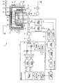
図1は、第1の実施形態に係るプラズマ処理装置10の構成例を示す図である。図1に示すプラズマ処理装置10は、容量結合プラズマ(CCP:Capacitively Coupled Plasma)を用いたプラズマ処理装置として構成される。プラズマ処理装置10は、略円筒状の処理容器12を備えている。処理容器12の内壁面は、例えば、陽極酸化処理されたアルミニウムから構成されている。この処理容器12は保安接地されている。
First Embodiment
FIG. 1 is a view showing a configuration example of a
処理容器12の底部上には、略円筒状の支持部14が設けられている。支持部14は、例えば、絶縁材料から構成されている。支持部14は、処理容器12内において、処理容器12の底部から鉛直方向に延在している。また、処理容器12内には、ウエハWの載置台として機能する下部電極18が設けられている。下部電極18は、支持部14によって支持されている。
A substantially
下部電極18は、その上面において被処理体としてのウエハWを保持する。下部電極18は、第1プレート18a及び第2プレート18bを含んでいる。第1プレート18a及び第2プレート18bは、例えばアルミアルミニウムといった金属から構成されており、略円盤形状をなしている。第2プレート18bは、第1プレート18a上に設けられており、第1プレート18aに電気的に接続されている。
The
下部電極18の第2プレート18b上には、静電チャック19が設けられている。静電チャック19は、導電膜である電極を一対の絶縁層又は絶縁シート間に配置した構造を有している。静電チャック19の電極には、直流電源22がスイッチ23を介して電気的に接続されている。この静電チャック19は、直流電源22からの直流電圧により生じたクーロン力等の静電力によりウエハWを吸着する。これにより、静電チャック19は、ウエハWを保持することができる。
An
下部電極18の第2プレート18bの周縁部上には、ウエハWのエッジ及び静電チャック19を囲むようにフォーカスリングFRが配置されている。フォーカスリングFRは、エッチングの均一性を向上させるために設けられている。フォーカスリングFRは、エッチング対象の膜の材料によって適宜選択される材料から構成されており、例えば、石英から構成され得る。
A focus ring FR is disposed on the periphery of the
第2プレート18bの内部には、冷媒流路24が設けられている。冷媒流路24は、温調機構を構成している。冷媒流路24には、処理容器12の外部に設けられたチラーユニットから配管26aを介して冷媒が供給される。冷媒流路24に供給された冷媒は、配管26bを介してチラーユニットに戻される。このように、冷媒流路24には、冷媒が循環するよう、供給される。この冷媒の温度を制御することにより、静電チャック19によって支持されたウエハWの温度が制御される。
A
また、プラズマ処理装置10には、ガス供給ライン28が設けられている。ガス供給ライン28は、伝熱ガス供給機構からの伝熱ガス、例えばHeガスを、静電チャック19の上面とウエハWの裏面との間に供給する。
Further, a
また、プラズマ処理装置10は、上部電極30を備えている。上部電極30は、下部電極18の上方において、当該下部電極18と対向配置されている。下部電極18と上部電極30とは、互いに略平行に設けられている。これら上部電極30と下部電極18との間には、ウエハWにプラズマ処理を行うための処理空間Sが提供されている。
The
上部電極30は、絶縁性遮蔽部材32を介して、処理容器12の上部に支持されている。また、上部電極30は、GNDに接続されている。第1の実施形態では、上部電極30は、下部電極18の上面、即ち、ウエハ載置面からの鉛直方向における距離が可変であるように構成され得る。上部電極30は、電極板34及び電極支持体36を含み得る。電極板34は処理空間Sに面しており、当該電極板34には複数のガス吐出孔34aが設けられている。この電極板34は、第1の実施形態では、シリコンから構成されている。
The
電極支持体36は、電極板34を着脱自在に支持するものであり、例えばアルミニウムといった導電性材料から構成され得る。この電極支持体36は、水冷構造を有し得る。電極支持体36の内部には、ガス拡散室36aが設けられている。このガス拡散室36aからは、ガス吐出孔34aに連通する複数のガス通流孔36bが下方に延びている。また、電極支持体36には、ガス拡散室36aに処理ガスを導くガス導入口36cが形成されており、このガス導入口36cには、ガス供給管38が接続されている。
The
ガス供給管38には、バルブ群42及び流量制御器群44を介して、ガスソース群40が接続されている。ガスソース群40は、フルオロカーボンガスのソース、希ガスのソース、及び、酸素(O2)ガスのソースといった複数のガスソースを含んでいる。フルオロカーボンガスは、例えば、C4F6ガス及びC4F8ガスのうち少なくとも一種を含むガスである。また、希ガスは、Arガス、Heガスといった種々の希ガスのうち少なくとも一種を含むガスである。
A
バルブ群42は複数のバルブを含んでおり、流量制御器群44はマスフローコントローラといった複数の流量制御器を含んでいる。ガスソース群40の複数のガスソースはそれぞれ、バルブ群42の対応のバルブ及び流量制御器群44の対応の流量制御器を介して、ガス供給管38に接続されている。
The
また、プラズマ処理装置10では、処理容器12の内壁に沿ってデポシールド46が着脱自在に設けられている。デポシールド46は、支持部14の外周にも設けられている。デポシールド46は、処理容器12にエッチング副生物(デポ)が付着することを防止するものであり、アルミニウム材にY2O3等のセラミックスを被覆することにより構成され得る。
In the
処理容器12の底部側、且つ、支持部14と処理容器12の側壁との間には排気プレート48が設けられている。排気プレート48は、例えば、アルミニウム材にY2O3等のセラミックスを被覆することにより構成され得る。この排気プレート48の下方、且つ、処理容器12には、排気口12eが設けられている。排気口12eには、排気管52を介して排気装置50が接続されている。排気装置50は、ターボ分子ポンプなどの真空ポンプを有しており、処理容器12内の空間を所望の真空度まで減圧することができる。また、処理容器12の側壁にはウエハWの搬入出口12gが設けられており、この搬入出口12gはゲートバルブ54により開閉可能となっている。
An
また、プラズマ処理装置10は、図1に示すように、高周波生成部61と、高周波電源64とを有する。
Further, as shown in FIG. 1, the
高周波生成部61は、予め定められた周波数を有する設定周波数成分を含む波形データを用いて、プラズマ生成用の高周波を生成する。高周波生成部61は、例えば、60MHzの周波数を有する設定周波数成分を含む波形データを用いて、60MHzの高周波を生成する。高周波生成部61は、増幅器62及び整合器63を介して下部電極18に接続されている。増幅器62は、高周波生成部61により生成される高周波を増幅し、増幅した高周波を整合器63を介して下部電極18へ供給する。整合器63は、高周波生成部61の出力インピーダンスと負荷側(つまり、下部電極18側)の入力インピーダンスを整合する。高周波生成部61と下部電極18との間の経路は、高周波生成部61により生成されたプラズマ生成用の高周波を下部電極18に伝送する経路であり、例えば、増幅器62、整合器63、及び、高周波生成部61と下部電極18とを接続するケーブル等の素子を備える。そして、これらの素子におけるインピーダンスの不連続点や微小な非線形特性によって、プラズマ生成用の高周波の周波数の整数倍の周波数に「高調波歪み」と呼ばれる歪み成分が生じる。「高調波歪み」は、高周波生成部61と下部電極18との間の経路において、プラズマ生成用の高周波に付加される。この「高調波歪み」は、高周波生成部61により生成されたプラズマ生成用の高周波を下部電極18に伝送する経路で生じる歪み成分の一例である。
The high
高周波生成部61は、図1に示すように、波形データ生成部71と、量子化部72と、逆フーリエ変換部73と、D(Digital)/A(Analog)変換部74,75と、LPF(Low Pass Filter)76,77とを有する。また、高周波生成部61は、PLL(Phase Locked Loop)発振器78と、移相器79と、乗算器80,81と、加算器82とを有する。
As shown in FIG. 1, the high
波形データ生成部71は、波形データを生成する。波形データ生成部71は、例えば、予め定められた周波数を有する設定周波数成分を含む波形データを生成する。そして、波形データ生成部71は、生成した波形データを量子化部72へ出力する。なお、波形データ生成部71により生成される波形データ、すなわち、高周波生成部61における第1の高周波の生成に用いられる波形データは、後述する波形補正部67によって補正される。
The waveform
量子化部72は、波形データ生成部71から入力される波形データを量子化する。逆フーリエ変換部73は、量子化部72により量子化された波形データを逆フーリエ変換することによって、波形データの同相成分データ(Iデータ:In-Phase component)及び逆相成分データ(Qデータ:Quadrature component)を分離する。逆フーリエ変換部73により分離された波形データのIデータ及びQデータは、D/A変換部74,75によってD/A変換され、LPF76,77を経て、乗算器80,81へ入力される。
The
PLL発振器78は、基準搬送波を生成し、生成した基準搬送波を移相器79及び乗算器80へ出力する。移相器79は、PLL発振器78から入力される基準搬送波の位相を90°シフトし、位相が90°シフトされた基準搬送波を乗算器81へ出力する。乗算器80は、LPF76から入力されるIデータと、PLL発振器78から入力される基準搬送波とを乗算する。乗算器81は、LPF77から入力されるQデータと、移相器79から入力される基準搬送波とを乗算する。加算器82は、乗算器80の乗算結果と、乗算器81の乗算結果とを合成することによって、プラズマ生成用の高周波を生成し、生成した高周波を増幅器62へ出力する。
The PLL oscillator 78 generates a reference carrier, and outputs the generated reference carrier to the
高周波電源64は、ウエハWにイオンを引き込むための高周波を生成する。高周波電源64は、高周波生成部61により生成される高周波よりも周波数が低い高周波を生成する。高周波電源64は、例えば、600kHzの高周波を生成する。以下では、高周波電源64により生成される高周波と、高周波生成部61により生成される高周波とを区別するために、高周波電源64により生成される高周波を「バイアス用高周波」と呼ぶ。高周波電源64は、整合器65を介して下部電極18に接続されている。整合器65は、高周波電源64の出力インピーダンスと負荷側(下部電極18側)の入力インピーダンスを整合する。高周波電源64は、高周波生成部61と同様に下部電極18に接続されているので、高周波生成部61により生成された高周波とは周波数が異なるバイアス用高周波が下部電極18に印加される場合、バイアス用高周波の一部が高周波生成部61と下部電極18との間の経路へ漏洩することがある。そして、高周波生成部61と下部電極18との間の経路へ漏洩したバイアス用高周波とプラズマ生成用の高周波とが干渉することにより、プラズマ生成用の高周波の周波数近傍に「混変調歪み」と呼ばれる歪み成分が生じる。「高調波歪み」は、高周波生成部61と下部電極18との間の経路において、プラズマ生成用の高周波に付加される。この「混変調歪み」は、高周波生成部61により生成された高周波を下部電極18に伝送する経路で生じる歪み成分の一例である。
The high
また、プラズマ処理装置10は、図1に示すように、歪み成分抽出部66と、波形補正部67とを有する。
Further, as shown in FIG. 1, the
歪み成分抽出部66は、高周波生成部61により生成されたプラズマ生成用の高周波を下部電極18に伝送する経路においてプラズマ生成用の高周波に付与される歪み成分を抽出する。歪み成分抽出部66により抽出される歪み成分には、例えば、上記の「高調波歪み」及び「混変調歪み」が含まれる。
The distortion
歪み成分抽出部66は、図1に示すように、電力測定部91,92と、A(Analog)/D(Digital)変換部93,94と、波形取得部95と、フーリエ変換部96と、比較部97とを有する。また、歪み成分抽出部66は、歪み成分を検出するために十分な高速応答性を有する必要があり、少なくとも基本周波数の2倍以上の高速応答性(周波数検出能力)を持ち、検出部分で波形の歪みおよび位相の変化が起こらないように設計される必要がある。すなわち、歪み成分抽出部66は、基本周波数の少なくとも2倍以上の周波数応答速度を持った電力、あるいは電圧の検出手段である。ここで、基本周波数は、波形データの補正により最終的にウェハW上で生成される正弦波の周波数(後述する図2Aにおいて設定周波数成分として定義されるf0の周波数)である。
The distortion
電力測定部91は、方向性結合器91aを介して、高周波生成部61と下部電極18との間の経路(図1の例では、整合器63の出力端)に接続されている。方向性結合器91aは、下部電極18へ向かうプラズマ生成用の高周波を抽出して電力測定部91へ出力する。電力測定部91は、方向性結合器91aから入力されるプラズマ生成用の高周波の電力(以下「高周波電力」と呼ぶ)を測定し、測定した高周波電力をA/D変換部93へ出力する。
The
電力測定部92は、方向性結合器92aを介して、高周波生成部61と下部電極18との間の経路(図1の例では、整合器63の出力端)に接続されている。方向性結合器92aは、プラズマ生成用の高周波がプラズマで反射された反射波を抽出して電力測定部92へ出力する。電力測定部92は、方向性結合器92aから入力される反射波の電力(以下「反射波電力」と呼ぶ)を測定し、測定した反射波電力をA/D変換部94へ出力する。
The
A/D変換部93は、電力測定部91から入力される高周波電力をA/D変換し、得られたデジタルの高周波電力を波形取得部95へ出力する。
The A / D conversion unit 93 A / D converts the high frequency power input from the
A/D変換部94は、電力測定部92から入力される反射波電力をA/D変換し、得られたデジタルの反射波電力を波形取得部95へ出力する。
The A / D conversion unit 94 A / D converts the reflected wave power input from the
波形取得部95は、高周波電力、又は、高周波電力と反射波電力との差分(つまり、高周波電力−反射波電力)に関して、波形を取得する。高周波電力と反射波電力との差分は、実際にプラズマに吸収された高周波の電力を示し、実効吸収電力とも呼ばれる。高周波電力又は実効吸収電力の波形は、下部電極18に印加される高周波の電圧波形と概ね一致する。このため、高周波電力又は実効吸収電力の波形には、高周波生成部61と下部電極18との間の経路においてプラズマ生成用の高周波に付加された歪み成分が含まれる。
The
フーリエ変換部96は、波形取得部95により取得された波形をフーリエ変換することによって、当該波形に含まれる複数の周波数成分を抽出し、抽出した複数の周波数成分を比較部97へ出力する。
The
比較部97は、波形に含まれる複数の周波数成分の入力をフーリエ変換部96から受ける。比較部97は、波形データ生成部71により生成される波形データに含まれる設定周波数成分を示す情報を予め保持している。そして、比較部97は、波形に含まれる複数の周波数成分と、設定周波数成分とを比較することによって、設定周波数成分以外の周波数成分を歪み成分として抽出し、抽出した歪み成分を波形補正部67へ出力する。
The
波形補正部67は、高周波生成部61における高周波の生成に用いられる波形データ、すなわち、波形データ生成部71により生成される波形データを補正する。具体的には、波形補正部67は、歪み成分抽出部66の比較部97から入力される歪み成分の位相を逆転して逆位相成分を得る。そして、波形補正部67は、歪み成分の逆位相成分を、波形データ生成部71により生成される波形データの設定周波数成分に合成することによって、当該波形データを補正する。波形補正部67により補正された波形データ(以下「補正後の波形データ」という)は、設定周波数成分に加えて、歪み成分の逆位相成分を含む。このため、補正後の波形データを用いて高周波生成部61により生成される高周波は、設定周波数成分に加えて、歪み成分の逆位相成分を含む。
The
図2A及び図2Bは、第1の実施形態における歪み成分抽出部66及び波形補正部67のよる処理の一例を説明するための図である。図2Aの右側の図は、高周波生成部61における高周波の生成に用いられる波形データ(つまり、波形データ生成部71により生成される波形データ)に含まれる設定周波数成分を示す。歪み成分抽出部66の比較部97は、図2Aの右側の図に示した設定周波数成分を示す情報を予め保持している。図2Aにおける左側の図は、フーリエ変換部96により抽出された複数の周波数成分(つまり、高周波電力又は実効吸収電力の波形に含まれる複数の周波数成分)を示す。
FIGS. 2A and 2B are diagrams for explaining an example of processing performed by the distortion
図2Aの左側の図に示すように、フーリエ変換部96により抽出された複数の周波数成分には、設定周波数成分に加えて、上記の「高調波歪み」及び「混変調歪み」が含まれる。図2Aの例では、「高調波歪み」は、設定周波数成分の周波数(つまり、高周波生成部61により生成されるプラズマ生成用の高周波の周波数)がf0であるとすると、2f0の周波数及び3f0の周波数に生じる。また、「混変調歪み」は、高周波電源64により生成されるバイアス用高周波の周波数がf1であるとすると、f0±f1の周波数及びf0±2f1の周波数に生じる。歪み成分抽出部66の比較部97は、図2Aの左側の図に示した複数の周波数成分と、図2Aの右側の図に示した設定周波数成分とを比較することによって、設定周波数成分以外の周波数成分である「高調波歪み」及び「混変調歪み」を歪み成分として抽出する。波形補正部67は、歪み成分として抽出された「高調波歪み」及び「混変調歪み」の位相を逆転して、「高調波歪み」の逆位相成分及び「混変調歪み」の逆位相成分を得る。そして、波形補正部67は、「高調波歪み」の逆位相成分及び「混変調歪み」の逆位相成分を、高周波生成部61における高周波の生成に用いられる波形データ(つまり、波形データ生成部71により生成される波形データ)の設定位相成分に合成することによって、当該波形データを補正する。補正後の波形データは、設定周波数成分に加えて、「高調波歪み」の逆位相成分及び「混変調歪み」の逆位相成分を含む。このため、補正後の波形データを用いて高周波生成部61により生成される高周波は、図2Bに示すように、設定周波数成分に加えて、「高調波歪み」の逆位相成分及び「混変調歪み」の逆位相成分を含む。
As shown in the left side of FIG. 2A, the plurality of frequency components extracted by the
ここで、図3及び図4を参照して、波形補正部67による波形データの補正のシミュレーション結果について説明する。図3は、波形補正部67による波形データの補正が行われる前の下部電極18の電圧波形のシミュレーション結果の一例を示す図である。図4は、波形補正部67による波形データの補正が行われた後の下部電極18の電圧波形のシミュレーション結果の一例を示す図である。
Here, simulation results of correction of waveform data by the
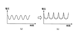
図3(a)は、波形補正部67により補正されていない波形データを用いて高周波生成部61により生成された高周波の電圧波形を示す。図3(b)は、図3(a)の電圧波形を有する高周波が高周波生成部61により生成された場合に下部電極18に印加される高周波の電圧波形を示す。図4(a)は、波形補正部67により補正された波形データを用いて高周波生成部61により生成された高周波の電圧波形を示す。図4(b)は、図4(a)の電圧波形を有する高周波が高周波生成部61により生成された場合に下部電極18に印加される高周波の電圧波形を示す。図3及び図4において、横軸は、時間を示し、縦軸は、高周波の電圧を示す。
FIG. 3A shows a high frequency voltage waveform generated by the high
図3のシミュレーション結果を参照すると、波形補正部67により波形データが補正されていない場合、高周波生成部61により生成された高周波の電圧波形は、正弦波である。また、波形補正部67により波形データが補正されていない場合、下部電極18に印加される高周波の電圧波形に歪みが生じる。すなわち、波形補正部67により波形データが補正されていない場合、高周波生成部61と下部電極18との間の経路において、プラズマ生成用の高周波に歪み成分が付与されるので、下部電極18に印加される高周波に波形歪みが生じる。
Referring to the simulation result of FIG. 3, when the
これに対して、図4のシミュレーション結果を参照すると、波形補正部67により波形データが補正された場合、補正後の波形データを用いて高周波生成部61により生成された高周波の電圧波形は、歪む。また、波形補正部67により波形データが補正された場合、下部電極18に印加される高周波の電圧波形は、正弦波である。すなわち、波形補正部67により波形データが補正された場合、高周波生成部61と下部電極18との間の経路においてプラズマ生成用の高周波に付与された歪み成分が歪み成分の逆位相成分によって相殺されるので、下部電極18に印加される高周波の波形歪みが抑制される。
On the other hand, referring to the simulation result of FIG. 4, when the
次に、第1の実施形態に係るプラズマ処理装置10における波形補正方法について説明する。図5は、第1の実施形態に係る波形補正方法の流れの一例を示すフローチャートである。
Next, a waveform correction method in the
図5に示すように、プラズマ処理装置10の高周波生成部61は、予め定められた周波数を有する設定周波数成分を含む波形データを用いて、高周波を生成する(ステップS101)。
As shown in FIG. 5, the high
歪み成分抽出部66は、高周波生成部61により生成されたプラズマ生成用の高周波を下部電極18に伝送する経路で生じる歪み成分を抽出する(ステップS102)。
The distortion
波形補正部67は、歪み成分の逆位相成分を、高周波生成部61における高周波の生成に用いられる波形データの設定周波数成分に合成することによって、当該波形データを補正する(ステップS103)。
The
本実施形態によれば、プラズマ生成用の高周波が印加され、かつ、ウエハWの載置台として機能する下部電極18を備えたプラズマ処理装置10において、予め定められた周波数を有する設定周波数成分を含む波形データを用いて、高周波を生成し、生成された高周波を下部電極18に伝送する経路で生じる歪み成分を抽出し、歪み成分の位相を逆転して得られる逆位相成分を、高周波の生成に用いられる波形データの設定周波数成分に合成することによって、波形データを補正する。これにより、高周波を下部電極18に伝送する経路においてプラズマ生成用の高周波に付与された歪み成分が歪み成分の逆位相成分によって相殺されるので、下部電極18に印加される高周波の波形歪みが抑制される。その結果、本実施形態によれば、下部電極18に印加される高周波の波形歪みに起因したエッチングレートの均一性の低下及び異なるプラズマ処理装置10間のエッチングレートの差を抑えることができる。
According to the present embodiment, in the
続いて、本実施形態に係る波形補正方法による効果についてさらに説明する。図6A及び図6Bは、第1の実施形態に係る波形補正方法による効果を説明するための図である。図6A及び図6Bの横軸は、ウエハWの中心位置「0」を基準とした径方向の位置を示す。図6A及び図6Bの縦軸は、ウエハWのエッチングレート(E/R)を示す。また、図6Aは、装置A〜装置Cについて、本実施形態に係る波形補正方法を用いずに、ウエハWに対してプラズマエッチング処理を実行した場合の、ウエハWの径方向の位置と、ウエハWのエッチングレートとの関係を示す。一方、図6Bは、装置A〜装置Cについて、本実施形態に係る波形補正方法を用いて、ウエハWに対してプラズマエッチング処理を実行した場合の、ウエハWの径方向の位置と、ウエハWのエッチングレートとの関係を示す。 Subsequently, the effects of the waveform correction method according to the present embodiment will be further described. 6A and 6B are diagrams for explaining the effect of the waveform correction method according to the first embodiment. The horizontal axes in FIGS. 6A and 6B indicate radial positions based on the center position “0” of the wafer W. The vertical axes in FIGS. 6A and 6B indicate the etching rate (E / R) of the wafer W. Further, FIG. 6A shows the position of the wafer W in the radial direction and the wafer when the plasma etching process is performed on the wafer W without using the waveform correction method according to the present embodiment for the apparatuses A to C. The relationship with the etching rate of W is shown. On the other hand, FIG. 6B shows the position of the wafer W in the radial direction and the wafer W when the plasma etching process is performed on the wafer W using the waveform correction method according to the present embodiment for the devices A to C. The relationship with the etching rate of
図6Aに示すように、本実施形態に係る波形補正方法を用いなかった場合、異なる装置A〜装置Cの各々におけるウエハWのエッチングレートの均一性が比較的に低下し、かつ、異なる装置A〜B間のエッチングレートの差が増大した。 As shown in FIG. 6A, when the waveform correction method according to this embodiment is not used, the uniformity of the etching rate of the wafer W in each of the different apparatuses A to C is relatively lowered, and the different apparatuses A are different. The difference in etching rate between -B was increased.
これに対して、本実施形態に係る波形補正方法を用いた場合、予め定められた周波数を有する設定周波数成分を含む波形データを用いて、高周波を生成し、生成された高周波を下部電極18に伝送する経路で生じる歪み成分を抽出し、歪み成分の位相を逆転して得られる逆位相成分を、高周波の生成に用いられる波形データの設定周波数成分に合成することによって、波形データを補正する。その結果、図6Bに示すように、本実施形態に係る波形補正方法を用いた場合、異なる装置A〜装置Cの各々におけるウエハWのエッチングレートの均一性が向上し、かつ、異なる装置A〜B間のエッチングレートの差が縮減された。
On the other hand, when the waveform correction method according to the present embodiment is used, a high frequency is generated using waveform data including a preset frequency component having a predetermined frequency, and the generated high frequency is used as the
(第2の実施形態)
第2の実施形態では、歪み成分を抽出する際に、高周波電力又は実効吸収電力に代えて、下部電極18の電圧値を測定して、波形を取得する点が第1の実施形態と異なる。以下の説明では、第1の実施形態と同一の構成要素については、同一の符号を付してその説明を省略する。
Second Embodiment
The second embodiment is different from the first embodiment in that the voltage value of the
図7は、第2の実施形態に係るプラズマ処理装置10の構成例を示す図である。図7に示すように、プラズマ処理装置10は、歪み成分抽出部166を有する。歪み成分抽出部166は、電圧測定部191と、A/D変換部193と、波形取得部195と、フーリエ変換部96と、比較部97とを有する。
FIG. 7 is a view showing a configuration example of a
電圧測定部191は、下部電極18の電圧値を測定する。具体的には、電圧測定部191は、高周波生成部61により生成された高周波を下部電極18に伝送する経路(つまり、高周波生成部61と下部電極18との間の経路)の電圧(以下「経路電圧」と呼ぶ)を下部電極18の自己バイアス電圧Vdcとして測定する。そして、電圧測定部191は、測定した経路電圧をA/D変換部193へ出力する。
The
A/D変換部193は、電圧測定部191から入力される経路電圧をA/D変換し、得られたデジタルの電圧を波形取得部195へ出力する。
The A / D conversion unit 193 A / D converts the path voltage input from the
波形取得部195は、下部電極18の電圧値、すなわち、経路電圧に関して、波形を取得する。経路電圧の波形は、下部電極18に印加される高周波の電圧波形と概ね一致する。このため、経路電圧の波形には、高周波生成部61と下部電極18との間の経路においてプラズマ生成用の高周波に付加された歪み成分が含まれる。
The
以上のように、本実施形態によれば、歪み成分を抽出する際に、下部電極18の電圧値(つまり、経路電圧)に関して、波形を取得する。その結果、本実施形態によれば、第1の実施形態と同様に、下部電極18に印加される高周波の波形歪みに起因したエッチングレートの均一性の低下及び異なる装置間のエッチングレートの差を抑えることができる。
As described above, according to the present embodiment, when the distortion component is extracted, the waveform is acquired with respect to the voltage value (that is, the path voltage) of the
(第3の実施形態)
第3の実施形態では、下部電極18の電圧値として静電チャック19の電圧を測定し、静電チャック19の電圧に関して、波形を取得する点が第2の実施形態と異なる。以下の説明では、第2の実施形態と同一の構成要素については、同一の符号を付してその説明を省略する。
Third Embodiment
The third embodiment is different from the second embodiment in that the voltage of the
図8は、第3の実施形態に係るプラズマ処理装置10の構成例を示す図である。図8に示すように、プラズマ処理装置10は、歪み成分抽出部266を有する。歪み成分抽出部266は、電圧測定部291と、A/D変換部293と、波形取得部295と、フーリエ変換部96と、比較部97とを有する。
FIG. 8 is a view showing a configuration example of a
電圧測定部291は、静電チャック19の電圧を下部電極18の自己バイアス電圧Vdcとして測定する。図8の例では、電圧測定部291は、静電チャック19と直流電源22とを接続する配線において、静電チャック19の電圧を測定する。そして、電圧測定部291は、測定した静電チャック19の電圧をA/D変換部293へ出力する。
The
A/D変換部293は、電圧測定部291から入力される静電チャック19の電圧をA/D変換し、得られたデジタルの電圧を波形取得部295へ出力する。
The A / D conversion unit 293 A / D converts the voltage of the
波形取得部295は、下部電極18の電圧値、すなわち、静電チャック19の電圧に関して、波形を取得する。静電チャック19の電圧の波形は、下部電極18に印加される高周波の電圧波形と概ね一致する。このため、静電チャック19の電圧の波形には、高周波生成部61と下部電極18との間の経路においてプラズマ生成用の高周波に付加された歪み成分が含まれる。
The
以上のように、本実施形態によれば、歪み成分を抽出する際に、下部電極18の電圧値(つまり、静電チャック19の電圧)に関して、波形を取得する。その結果、本実施形態によれば、第2の実施形態と同様に、下部電極18に印加される高周波の波形歪みに起因したエッチングレートの均一性の低下及び異なる装置間のエッチングレートの差を抑えることができる。
As described above, according to the present embodiment, when the strain component is extracted, a waveform is acquired regarding the voltage value of the lower electrode 18 (that is, the voltage of the electrostatic chuck 19). As a result, according to the present embodiment, as in the second embodiment, the uniformity of the etching rate due to the waveform distortion of the high frequency applied to the
(第4の実施形態)
第4の実施形態では、下部電極18の電圧値としてフォーカスリングFRの電圧を測定し、フォーカスリングFRの電圧に関して、波形を取得する点が第2の実施形態と異なる。以下の説明では、第2の実施形態と同一の構成要素については、同一の符号を付してその説明を省略する。
Fourth Embodiment
The fourth embodiment is different from the second embodiment in that the voltage of the focus ring FR is measured as the voltage value of the
図9は、第4の実施形態に係るプラズマ処理装置10の構成例を示す図である。図9に示すように、プラズマ処理装置10は、歪み成分抽出部366を有する。歪み成分抽出部366は、電圧測定部391と、A/D変換部393と、波形取得部395と、フーリエ変換部96と、比較部97とを有する。
FIG. 9 is a view showing a configuration example of a
電圧測定部391は、フォーカスリングFRの電圧値を測定する。そして、電圧測定部391は、測定したフォーカスリングFRの電圧をA/D変換部393へ出力する。
The
A/D変換部393は、電圧測定部391から入力されるフォーカスリングFRの電圧をA/D変換し、得られたデジタルの電圧を波形取得部395へ出力する。
The A / D conversion unit 393 A / D converts the voltage of the focus ring FR input from the
波形取得部395は、下部電極18の電圧値、すなわち、フォーカスリングFRの電圧に関して、波形を取得する。フォーカスリングFRの電圧の波形は、下部電極18に印加される高周波の電圧波形と概ね一致する。このため、フォーカスリングFRの電圧の波形には、高周波生成部61と下部電極18との間の経路においてプラズマ生成用の高周波に付加された歪み成分が含まれる。
The
以上のように、本実施形態によれば、歪み成分を抽出する際に、下部電極18の電圧値に関して、波形を取得する。その結果、本実施形態によれば、第2の実施形態と同様に、下部電極18に印加される高周波の波形歪みに起因したエッチングレートの均一性の低下及び異なる装置間のエッチングレートの差を抑えることができる。
As described above, according to the present embodiment, when the distortion component is extracted, the waveform is acquired regarding the voltage value of the
10 プラズマ処理装置
12 処理容器
18 下部電極
18a 第1プレート
18b 第2プレート
19 静電チャック
30 上部電極
61 高周波生成部
62 増幅器
63 整合器
64 高周波電源
65 整合器
66、166、266、366 歪み成分抽出部
67 波形補正部
91、92 電力測定部
95、195、295、395 波形取得部
96 フーリエ変換部
97 比較部
191、291、391 電圧測定部
FR フォーカスリング
DESCRIPTION OF
Claims (6)
予め定められた周波数を有する設定周波数成分を含む波形データを用いて、プラズマ生成用の高周波を生成する高周波生成部と、
前記高周波生成部により生成された前記高周波を前記電極に伝送する経路において前記高周波に付与される歪み成分を抽出する歪み成分抽出部と、
前記歪み成分の位相を逆転して得られる逆位相成分を、前記高周波生成部における前記高周波の生成に用いられる波形データの前記設定周波数成分に合成することによって、前記波形データを補正する波形補正部と
を有することを特徴とするプラズマ処理装置。 A plasma processing apparatus having a conductive electrode,
A high frequency generating unit for generating a high frequency for plasma generation using waveform data including a set frequency component having a predetermined frequency;
A distortion component extraction unit for extracting distortion components applied to the high frequency in a path for transmitting the high frequency generated by the high frequency generation unit to the electrode;
A waveform correction unit that corrects the waveform data by combining an antiphase component obtained by reversing the phase of the distortion component with the set frequency component of waveform data used for generating the high frequency in the high frequency generation unit. And a plasma processing apparatus characterized by having.
前記電極に印加される前記高周波の電力、前記高周波の電力と前記高周波がプラズマで反射された反射波の電力との差分、又は前記電極の電圧値に関して、波形を取得する波形取得部と、
前記波形をフーリエ変換することによって、前記波形に含まれる複数の周波数成分を抽出するフーリエ変換部と、
前記複数の周波数成分と、前記設定周波数成分とを比較することによって、前記設定周波数成分以外の周波数成分を前記歪み成分として抽出する比較部と
を有することを特徴とする請求項1に記載のプラズマ処理装置。 The distortion component extraction unit
A waveform acquisition unit that acquires a waveform regarding the power of the high frequency applied to the electrode, the difference between the power of the high frequency and the power of the reflected wave of the high frequency reflected by the plasma, or the voltage value of the electrode;
A Fourier transform unit that extracts a plurality of frequency components included in the waveform by Fourier transforming the waveform;
The plasma processing apparatus according to claim 1, further comprising: a comparison unit that extracts frequency components other than the set frequency component as the distortion component by comparing the plurality of frequency components with the set frequency component. Processing unit.
前記高周波生成部により生成された前記高周波を前記電極に伝送する経路の電圧を前記電極の電圧値として測定する電圧測定部をさらに有し、
前記波形取得部は、
前記電圧測定部により測定された前記経路の電圧に関して、波形を取得することを特徴とする請求項2に記載のプラズマ処理装置。 The distortion component extraction unit
The voltage measuring unit further includes a voltage measuring unit configured to measure a voltage of a path for transmitting the high frequency generated by the high frequency generating unit to the electrode as a voltage value of the electrode.
The waveform acquisition unit
The plasma processing apparatus according to claim 2, wherein a waveform is acquired regarding the voltage of the path measured by the voltage measurement unit.
前記電極上には、前記被処理体を静電力により吸着する静電チャックが設けられ、
前記歪み成分抽出部は、
前記静電チャックの電圧を前記電極の電圧値として測定する電圧測定部をさらに有し、
前記波形取得部は、
前記電圧測定部により測定された前記静電チャックの電圧に関して、波形を取得することを特徴とする請求項2に記載のプラズマ処理装置。 The electrode functions as a mounting table for the object to be processed.
An electrostatic chuck is provided on the electrode for attracting the object by electrostatic force.
The distortion component extraction unit
It further has a voltage measurement unit that measures the voltage of the electrostatic chuck as the voltage value of the electrode,
The waveform acquisition unit
The plasma processing apparatus according to claim 2, wherein a waveform is acquired regarding the voltage of the electrostatic chuck measured by the voltage measurement unit.
前記電極上には、前記被処理体が載置される領域を囲むようにフォーカスリングが設けられ、
前記歪み成分抽出部は、
前記フォーカスリングの電圧を前記電極の電圧値として測定する電圧測定部をさらに有し、
前記波形取得部は、
前記電圧測定部により測定された前記フォーカスリングの電圧に関して、波形を取得することを特徴とする請求項2に記載のプラズマ処理装置。 The electrode functions as a mounting table for the object to be processed.
A focus ring is provided on the electrode so as to surround a region on which the object to be processed is placed;
The distortion component extraction unit
It further has a voltage measurement unit that measures the voltage of the focus ring as the voltage value of the electrode,
The waveform acquisition unit
The plasma processing apparatus according to claim 2, wherein a waveform is acquired regarding the voltage of the focus ring measured by the voltage measurement unit.
予め定められた周波数を有する設定周波数成分を含む波形データを用いて、プラズマ生成用の高周波を生成し、
生成された前記高周波を前記電極に伝送する経路において前記高周波に付与される歪み成分を抽出し、
前記歪み成分の位相を逆転して得られる逆位相成分を、前記高周波の生成に用いられる波形データの前記設定周波数成分に合成することによって、前記波形データを補正する
ことを特徴とする波形補正方法。 A waveform correction method in a plasma processing apparatus having electrodes,
Generating high frequency for plasma generation using waveform data including a set frequency component having a predetermined frequency;
Extracting a distortion component to be applied to the high frequency in a path for transmitting the generated high frequency to the electrode;
A waveform correction method characterized by correcting the waveform data by combining an anti-phase component obtained by reversing the phase of the distortion component with the set frequency component of the waveform data used to generate the high frequency. .
Priority Applications (4)
| Application Number | Priority Date | Filing Date | Title |
|---|---|---|---|
| JP2016121596A JP6541623B2 (en) | 2016-06-20 | 2016-06-20 | Plasma processing apparatus and waveform correction method |
| TW106118818A TWI794176B (en) | 2016-06-20 | 2017-06-07 | Plasma treatment device and waveform correction method |
| KR1020170077136A KR102358730B1 (en) | 2016-06-20 | 2017-06-19 | Plasma processing apparatus and waveform correction method |
| US15/626,502 US9934947B2 (en) | 2016-06-20 | 2017-06-19 | Plasma processing apparatus and waveform correction method |
Applications Claiming Priority (1)
| Application Number | Priority Date | Filing Date | Title |
|---|---|---|---|
| JP2016121596A JP6541623B2 (en) | 2016-06-20 | 2016-06-20 | Plasma processing apparatus and waveform correction method |
Publications (3)
| Publication Number | Publication Date |
|---|---|
| JP2017228558A JP2017228558A (en) | 2017-12-28 |
| JP2017228558A5 JP2017228558A5 (en) | 2018-08-16 |
| JP6541623B2 true JP6541623B2 (en) | 2019-07-10 |
Family
ID=60659760
Family Applications (1)
| Application Number | Title | Priority Date | Filing Date |
|---|---|---|---|
| JP2016121596A Active JP6541623B2 (en) | 2016-06-20 | 2016-06-20 | Plasma processing apparatus and waveform correction method |
Country Status (4)
| Country | Link |
|---|---|
| US (1) | US9934947B2 (en) |
| JP (1) | JP6541623B2 (en) |
| KR (1) | KR102358730B1 (en) |
| TW (1) | TWI794176B (en) |
Families Citing this family (14)
| Publication number | Priority date | Publication date | Assignee | Title |
|---|---|---|---|---|
| JP7037964B2 (en) * | 2018-03-09 | 2022-03-17 | 東京エレクトロン株式会社 | How the system operates to inspect the measuring instrument and focus ring |
| JP6846384B2 (en) * | 2018-06-12 | 2021-03-24 | 東京エレクトロン株式会社 | Method of controlling high frequency power supply of plasma processing equipment and plasma processing equipment |
| US10916409B2 (en) * | 2018-06-18 | 2021-02-09 | Lam Research Corporation | Active control of radial etch uniformity |
| JP6842443B2 (en) * | 2018-06-22 | 2021-03-17 | 東京エレクトロン株式会社 | Plasma processing equipment and method of generating plasma |
| CN113169026B (en) * | 2019-01-22 | 2024-04-26 | 应用材料公司 | Feedback loop for controlling pulse voltage waveform |
| JP7122268B2 (en) * | 2019-02-05 | 2022-08-19 | 東京エレクトロン株式会社 | Plasma processing equipment |
| US11721526B2 (en) * | 2019-05-31 | 2023-08-08 | Mks Instruments, Inc. | System and method of power generation with phase linked solid-state generator modules |
| KR102175086B1 (en) * | 2019-07-15 | 2020-11-05 | 세메스 주식회사 | Apparatus for treating substrate and method for treating apparatus |
| CN113035677B (en) * | 2019-12-09 | 2023-01-24 | 中微半导体设备(上海)股份有限公司 | Plasma processing apparatus and plasma processing method |
| WO2021124427A1 (en) * | 2019-12-17 | 2021-06-24 | 株式会社日立ハイテク | Plasma processing apparatus and method for operating plasma processing apparatus |
| JP2021168231A (en) * | 2020-04-09 | 2021-10-21 | 東京計器株式会社 | High frequency generation device |
| US11775199B2 (en) * | 2021-01-20 | 2023-10-03 | Micron Technology, Inc. | Voltage resonance mitigation of memory dies |
| KR20240042091A (en) * | 2021-08-12 | 2024-04-01 | 램 리써치 코포레이션 | Distortion of pulses for wafer biasing |
| JP2024062195A (en) | 2022-10-24 | 2024-05-09 | 東京エレクトロン株式会社 | Frequency variable power supply and plasma processing device |
Family Cites Families (19)
| Publication number | Priority date | Publication date | Assignee | Title |
|---|---|---|---|---|
| US5965034A (en) * | 1995-12-04 | 1999-10-12 | Mc Electronics Co., Ltd. | High frequency plasma process wherein the plasma is executed by an inductive structure in which the phase and anti-phase portion of the capacitive currents between the inductive structure and the plasma are balanced |
| US6252354B1 (en) * | 1996-11-04 | 2001-06-26 | Applied Materials, Inc. | RF tuning method for an RF plasma reactor using frequency servoing and power, voltage, current or DI/DT control |
| JP3808973B2 (en) * | 1996-05-15 | 2006-08-16 | 株式会社ダイヘン | Plasma processing equipment |
| JP3122618B2 (en) * | 1996-08-23 | 2001-01-09 | 東京エレクトロン株式会社 | Plasma processing equipment |
| JPH10241895A (en) | 1996-11-04 | 1998-09-11 | Applied Materials Inc | Improvement of plasma process efficiency by filtering plasma sheath generation harmonic |
| US20010045832A1 (en) * | 1997-11-26 | 2001-11-29 | Kenneth W. Belt | Peripheral vascular array |
| JP4633881B2 (en) * | 2000-02-21 | 2011-02-16 | 株式会社日立製作所 | Plasma processing apparatus and processing method using the same |
| CA2373139A1 (en) * | 2000-06-12 | 2001-12-20 | Sysmex Corporation | Immunoassay and immunoassay apparatus |
| TW201041455A (en) * | 2002-12-16 | 2010-11-16 | Japan Science & Tech Agency | Plasma generation device, plasma control method, and substrate manufacturing method |
| US8835869B2 (en) * | 2003-02-04 | 2014-09-16 | Veeco Instruments, Inc. | Ion sources and methods for generating an ion beam with controllable ion current density distribution |
| JP4408707B2 (en) | 2004-01-13 | 2010-02-03 | 株式会社日立ハイテクノロジーズ | Plasma processing equipment |
| JP4920991B2 (en) * | 2006-02-22 | 2012-04-18 | 株式会社日立ハイテクノロジーズ | Plasma processing apparatus and plasma processing method |
| JP5376816B2 (en) * | 2008-03-14 | 2013-12-25 | 東京エレクトロン株式会社 | Microwave introduction mechanism, microwave plasma source, and microwave plasma processing apparatus |
| JP4978566B2 (en) * | 2008-06-10 | 2012-07-18 | パナソニック株式会社 | Atmospheric pressure plasma generation method and apparatus |
| US9111795B2 (en) * | 2011-04-29 | 2015-08-18 | Semiconductor Energy Laboratory Co., Ltd. | Semiconductor device with capacitor connected to memory element through oxide semiconductor film |
| JP2014049362A (en) * | 2012-09-03 | 2014-03-17 | Tokyo Electron Ltd | Plasma generation device and substrate processing device |
| US9924883B2 (en) * | 2013-06-28 | 2018-03-27 | University of Pittsburgh—of the Commonwealth System of Higher Education | Biomimetic coating for neural implants |
| JP6140093B2 (en) * | 2014-03-18 | 2017-05-31 | 株式会社東芝 | Cache memory, error correction circuit, and processor system |
| US9798256B2 (en) * | 2015-06-30 | 2017-10-24 | Canon Kabushiki Kaisha | Method of producing toner |
-
2016
- 2016-06-20 JP JP2016121596A patent/JP6541623B2/en active Active
-
2017
- 2017-06-07 TW TW106118818A patent/TWI794176B/en active
- 2017-06-19 US US15/626,502 patent/US9934947B2/en active Active
- 2017-06-19 KR KR1020170077136A patent/KR102358730B1/en active IP Right Grant
Also Published As
| Publication number | Publication date |
|---|---|
| US9934947B2 (en) | 2018-04-03 |
| JP2017228558A (en) | 2017-12-28 |
| US20170365445A1 (en) | 2017-12-21 |
| KR20170142925A (en) | 2017-12-28 |
| KR102358730B1 (en) | 2022-02-04 |
| TWI794176B (en) | 2023-03-01 |
| TW201810419A (en) | 2018-03-16 |
Similar Documents
| Publication | Publication Date | Title |
|---|---|---|
| JP6541623B2 (en) | Plasma processing apparatus and waveform correction method | |
| CN111029238B (en) | Plasma processing apparatus and control method | |
| WO2019244734A1 (en) | Control method and plasma treatment device | |
| KR20210019400A (en) | Control method and plasma processing device | |
| JP7000521B2 (en) | Plasma processing equipment and control method | |
| US20130284369A1 (en) | Two-phase operation of plasma chamber by phase locked loop | |
| KR20200083330A (en) | Plasma processing apparatus and control method | |
| CN111293024B (en) | Control method and plasma processing apparatus | |
| JP6625122B2 (en) | Plasma processing apparatus and plasma processing method | |
| TW201802934A (en) | Plasma processing device | |
| JP6817889B2 (en) | Plasma processing equipment and plasma processing method | |
| JP2021068880A (en) | Suction method, placing platform, and plasma processing device | |
| JP2023001473A (en) | Plasma processing apparatus and plasma processing method | |
| KR102421082B1 (en) | Rf tailored voltage on bias operation | |
| US9859101B2 (en) | Plasma processing apparatus and plasma processing method | |
| JP7442365B2 (en) | Substrate processing apparatus, substrate processing system, control method for substrate processing apparatus, and control method for substrate processing system | |
| WO2023074816A1 (en) | Plasma treatment device, power supply system, control method, program, and storage medium | |
| US20240136154A1 (en) | Frequency-variable power supply and plasma processing apparatus | |
| JP2007115867A (en) | Plasma processor and method for controlling the same | |
| JP2020119938A (en) | Substrate processing apparatus and substrate processing method |
Legal Events
| Date | Code | Title | Description |
|---|---|---|---|
| A521 | Request for written amendment filed |
Free format text: JAPANESE INTERMEDIATE CODE: A523 Effective date: 20180706 |
|
| A621 | Written request for application examination |
Free format text: JAPANESE INTERMEDIATE CODE: A621 Effective date: 20180906 |
|
| TRDD | Decision of grant or rejection written | ||
| A977 | Report on retrieval |
Free format text: JAPANESE INTERMEDIATE CODE: A971007 Effective date: 20190426 |
|
| A01 | Written decision to grant a patent or to grant a registration (utility model) |
Free format text: JAPANESE INTERMEDIATE CODE: A01 Effective date: 20190514 |
|
| A61 | First payment of annual fees (during grant procedure) |
Free format text: JAPANESE INTERMEDIATE CODE: A61 Effective date: 20190611 |
|
| R150 | Certificate of patent or registration of utility model |
Ref document number: 6541623 Country of ref document: JP Free format text: JAPANESE INTERMEDIATE CODE: R150 |
|
| R250 | Receipt of annual fees |
Free format text: JAPANESE INTERMEDIATE CODE: R250 |
|
| R250 | Receipt of annual fees |
Free format text: JAPANESE INTERMEDIATE CODE: R250 |
|
| R250 | Receipt of annual fees |
Free format text: JAPANESE INTERMEDIATE CODE: R250 |