JP6530976B2 - Connector cap - Google Patents
Connector cap Download PDFInfo
- Publication number
- JP6530976B2 JP6530976B2 JP2015126551A JP2015126551A JP6530976B2 JP 6530976 B2 JP6530976 B2 JP 6530976B2 JP 2015126551 A JP2015126551 A JP 2015126551A JP 2015126551 A JP2015126551 A JP 2015126551A JP 6530976 B2 JP6530976 B2 JP 6530976B2
- Authority
- JP
- Japan
- Prior art keywords
- connector
- cap
- housing
- mounting
- insertion hole
- Prior art date
- Legal status (The legal status is an assumption and is not a legal conclusion. Google has not performed a legal analysis and makes no representation as to the accuracy of the status listed.)
- Active
Links
Images


Description
本発明は、コネクタを基板に実装する際に使用されるコネクタ用のキャップに関する。 The present invention relates to a cap for a connector used when mounting the connector to a substrate.
基板上にコネクタを実装する方法として、リフロー半田付け法が知られている。これは、コネクタに設けられる吸着面を吸着ヘッドで吸着して基板上の所定位置に搬送し、その後、基板及びコネクタを加熱炉内に配置して基板上に設けられるクリーム半田を融かしてコネクタの端子を基板上の配線に半田付けする方法である。しかし、コネクタの中には、吸着ヘッドにより吸着可能な吸着面を上部に有していないものがある。こうしたコネクタを基板に実装する場合には、吸着面を有するコネクタ用のキャップをコネクタに取り付け、吸着ヘッドをその吸着面に吸着させることによりコネクタを所定位置に搬送する方法が取られることがある(例として特許文献1)。 As a method of mounting a connector on a substrate, a reflow soldering method is known. In this method, the suction surface provided on the connector is suctioned by the suction head and conveyed to a predetermined position on the substrate, and then the substrate and the connector are placed in a heating furnace to melt the cream solder provided on the substrate This is a method of soldering the terminal of the connector to the wiring on the substrate. However, some connectors do not have a suction surface at the top that can be suctioned by a suction head. When such a connector is mounted on a substrate, a method of attaching a cap for a connector having a suction surface to the connector and suctioning the suction head to the suction surface may be employed to transport the connector to a predetermined position (S. Patent document 1) as an example.
しかしながら、こうしたコネクタ用のキャップはコネクタが有する接続対象物の挿入口を閉塞するため、コネクタ用のキャップを取り付けたままではコネクタに接続対象物を挿入することができない。よって、コネクタを基板に実装した後でコネクタ用のキャップを取り外す必要があるため、作業効率に問題がある場合がある。 However, since the cap for such a connector closes the insertion port of the connection object of the connector, the connection object can not be inserted into the connector with the connector cap attached. Therefore, since it is necessary to remove the cap for connectors after mounting a connector on a board | substrate, there may be a problem in working efficiency.
本発明は、このような従来技術を背景になされたものである。その目的は、コネクタの実装作業を効率よく行うことができるコネクタ用のキャップを提供するものである。 The present invention is made in the background of such prior art. An object of the present invention is to provide a cap for a connector capable of efficiently performing a connector mounting operation.
上記目的を達成すべく本発明は以下のように構成される。
すなわち、本発明はコネクタのハウジングを保持する装着部と、前記ハウジングに備わるコネクタの接続対象物の挿入口に沿って設けられるカバー部とを有しており、該カバー部が、前記ハウジングの挿入口と連通し、接続対象物を挿入する挿通孔を有するコネクタ用のキャップを提供する。
In order to achieve the above object, the present invention is configured as follows.
That is, the present invention has a mounting portion for holding the housing of the connector, and a cover portion provided along the insertion port of the connection target of the connector provided on the housing, and the cover portion is the insertion of the housing. Provided is a cap for a connector in communication with a port and having an insertion hole for inserting a connection object.
ハウジングを保持する装着部を有するため、コネクタを基板に実装する際に本発明のコネクタ用のキャップを持ち上げて移送することで、コネクタを装着部に追従させて同時に移送することができる。したがって、ハウジングがコネクタの移送時に保持される部分を有さない場合であっても、容易にコネクタを移送して基板に実装することができる。また、本発明のカバー部が、前記ハウジングの挿入口と連通し、接続対象物を挿通する挿通孔を有することで、コネクタ用のキャップをハウジングに取り付けた状態で接続対象物を、挿通孔を通じて挿入口に挿入することができる。よって、接続対象物をコネクタに挿入するためにコネクタ用のキャップをハウジングから取り外す必要がないため、基板へのコネクタの実装作業を効率よく行うことができる。また、こうした挿通孔が接続対象物の先端をハウジングの挿入口までガイドするため、接続対象物を挿入口にスムーズに挿入することができる。 Since the mounting portion for holding the housing is provided, by lifting and transferring the cap for the connector of the present invention when mounting the connector on the substrate, the connector can be made to follow the mounting portion and be simultaneously transferred. Therefore, even when the housing does not have a portion to be held during transfer of the connector, the connector can be easily transferred and mounted on the substrate. Further, the cover portion of the present invention communicates with the insertion port of the housing and has an insertion hole through which the connection object is inserted, whereby the connection object is attached to the housing through the insertion hole while the cap for the connector is attached to the housing. It can be inserted into the insertion slot. Therefore, since it is not necessary to remove the cap for connectors from a housing in order to insert a connection subject into a connector, the mounting operation of a connector to a substrate can be performed efficiently. Further, since the insertion hole guides the tip of the connection object to the insertion port of the housing, the connection object can be smoothly inserted into the insertion port.
前記本発明は、接続対象物の非挿入状態で前記挿通孔を閉塞し、前記接続対象物を挿入する際に押圧されて前記挿通孔を開放するシャッター部を有するものとすることができる。 In the present invention, the insertion hole may be closed in a non-insertion state of the connection object, and the shutter portion may have a shutter portion which is pressed when the connection object is inserted and opens the insertion hole.
接続対象物の非挿入状態において、シャッター部が挿通孔を閉塞することで、挿入口からハウジングの内部に異物を入り込ませ難くすることができる。接続対象物を挿通し、その後抜去することで、シャッター部が挿通孔を再度閉塞する構造とすることで、接続対象物の挿抜を繰り返しても、確実にハウジングの内部に異物を入り込ませ難くすることができる。 In the non-insertion state of the connection object, the shutter portion closes the insertion hole, thereby making it difficult for foreign matter to enter the inside of the housing from the insertion port. By inserting the connection object and removing it thereafter, the shutter portion closes the insertion hole again, so that foreign objects can not be reliably made to enter the inside of the housing even if the connection object is repeatedly inserted and removed. be able to.
前記本発明は、複数の前記装着部と、少なくとも1つの前記挿通孔とを有しており、各装着部にコネクタのハウジングを保持するものとすることができる。 The present invention may include a plurality of the mounting portions and at least one the insertion hole, and the housing of the connector may be held by each mounting portion.
複数のコネクタを基板に実装する場合、コネクタを1つずつ実装すると、時間と手間が掛かって作業効率に問題がある。また、実装作業の回数が増えると、目的位置に実装されないコネクタが増える場合もある。この場合、基板によってコネクタ同士の間隔にばらつきが生じ、コネクタによっては基板上の回路と正確に導通接続できなくなるといった不具合が生じるおそれもあり、問題となる。そこで、複数の前記装着部と、少なくとも1つの前記挿通孔とを有しており、各装着部にコネクタのハウジングを保持するコネクタ用のキャップとすることで、複数のコネクタにキャップを装着して、それらを同時に移送することができる。こうすることで、実装作業を効率よく行うことができる。また、基板によってコネクタ同士の間隔をばらつかせずに、一定にすることができる。そのため、より正確な位置に複数のコネクタを実装することができる。 In the case of mounting a plurality of connectors on a substrate, mounting the connectors one by one takes time and labor and causes a problem in work efficiency. In addition, when the number of mounting operations increases, the number of connectors not mounted at the target position may increase. In this case, the gap between the connectors may vary depending on the substrate, and there may be a problem that the connector can not be correctly connected to the circuit on the substrate depending on the connector. Therefore, a plurality of mounting parts and at least one insertion hole are provided, and the mounting parts are mounted on the plurality of connectors by using a cap for the connector which holds the housing of the connector in each mounting part. , They can be transported simultaneously. By doing this, the mounting work can be performed efficiently. In addition, the distance between the connectors can be made constant by the substrate. Therefore, multiple connectors can be mounted at more accurate positions.
前記本発明は、カバー部が、コネクタ移送時の吸着面を有するものとすることができる。 In the present invention, the cover portion can have a suction surface at the time of connector transfer.
カバー部が吸着ヘッドの吸着面を有することで、こうした吸着面を有さないコネクタであっても、リフロー半田等による自動実装を容易に行うことができる。 With the cover portion having the suction surface of the suction head, automatic mounting by reflow soldering or the like can be easily performed even with a connector having no suction surface.
本発明によれば、コネクタに取り付けた状態で、接続対象物をコネクタに挿入可能なコネクタ用のキャップを提供することができる。コネクタからコネクタ用のキャップを取り外す作業を省略することができるため、基板へのコネクタの実装作業を効率よく行うことができる。 According to the present invention, it is possible to provide a cap for a connector capable of inserting an object to be connected into the connector in a state of being attached to the connector. Since the work of removing the connector cap from the connector can be omitted, the work of mounting the connector on the substrate can be performed efficiently.
以下、本発明の実施形態について図面を参照しつつ説明する。以下の各実施形態で共通する構成については、同一の符号を付して重複説明を省略する。 Hereinafter, embodiments of the present invention will be described with reference to the drawings. The same reference numerals are given to configurations common to each of the following embodiments, and redundant description will be omitted.
本実施形態のコネクタ用のキャップ1,5,6はコネクタ2に取り付けられて使用されるものであり、平型導体4を挿通する挿通部1a2を有する。本明細書中では、各キャップ1,5,6の挿通孔1a2に挿通される「接続対象物」としての平型導体4の板幅方向(幅方向)をX方向、平型導体4の板厚方向(前後方向)をY方向、各キャップ1,5,6に対する平型導体4の挿抜方向(上下方向)をZ方向として説明する。また、各キャップ1,5,6をコネクタ2に取り付けた状態において、挿抜方向Zにおけるコネクタ2の側を「下側」とし、各キャップ1,5,6の側を「上側」として説明し、また、板厚方向Yにおいてコネクタ2のレバー部2eが設けられる側を「前側」とし、反対側を「後側」として説明する。しかし、これらの記載によって各キャップ1,5,6の実装方法や使用方法を限定するものではない。なお、左側面図は右側面図とは左右対称に表されるため、記載を省略する。
本実施形態の各キャップ1,5,6が装着されるコネクタとしては、基板3に実装された状態で、基板3に対する垂直方向で平型導体4が挿入されるコネクタ2を例示する。またコネクタ2は、図8〜図13で示すように、ハウジング2aと、端子2bと、グラウンド端子2cと、平型導体4をハウジング2aの内部に挿入する挿入口2d1と、ハウジング2aに挿入した平型導体4をハウジング2aに対して着脱可能に固定するレバー部2eとを有する。
As a connector with which each
コネクタ2をリフロー半田によって基板3に実装する場合、通常、コネクタ2の上側には吸着ヘッド(図示略)を吸着するための平坦な吸着部を必要とする。しかし、コネクタ2は上記の通り、基板に対する垂直方向で平型導体4を挿入するものであり、コネクタ2の上壁部2dには挿入口2d1が開口するため、上壁部2dは吸着ヘッド(図示略)が吸着できるだけの面積を有さない。また、グラウンド端子2cが挿入口2d1よりも上側に突出する場合には、やはり吸着ヘッドで上壁部2dを吸着することが困難である。なお、コネクタ用のキャップ1,5,6が装着されるコネクタはこうしたコネクタ2には限られない。例えばグラウンド端子2cやレバー部2eを有していないコネクタについても装着可能である。
When the
第1実施形態〔図1〜図13〕:
本実施形態のコネクタ用のキャップ1は、コネクタ2の上壁部2d側に装着されて使用される。
First Embodiment [FIGS. 1 to 13]:
The
〔コネクタ用のキャップの構成〕
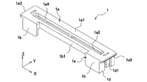
コネクタ用のキャップ1は絶縁性樹脂でなり、略直方体形状でなる。また、コネクタ用のキャップ1は、図1〜図7で示すように、カバー部1aと、装着部1eとを有する。装着部1eは、前壁部1bと、後壁部1cと、側壁部1d,1dとを有する。
[Configuration of cap for connector]
The
カバー部1aは、コネクタ用のキャップ1がコネクタ2のハウジング2aに取り付けられた状態で、コネクタ2の上壁部2d及び上壁部2dに設けられる挿入口2d1に沿うように設けられる。カバー部1aは、基板3と平行で、平坦な吸着面1e1を有する。吸着面1a1は幅方向X及び前後方向Yで、コネクタ2の上壁部2dよりも大きく形成され、吸着ノズルによって真空吸着可能な面積を有する。また、カバー部1aは幅方向Xにおける両端側に、後述する側壁部1d,1dよりもさらに幅方向Xに沿って突出する突出部1a3を有する。コネクタ用のキャップ1をコネクタ2に取り付けた後、コネクタ2から取り外す場合には、この突出部1a3に指などを引っ掛けることで容易に取り外し作業を行うことができる。
The
カバー部1aの幅方向Xにおける略中央であって、かつ前後方向Yにおける略中央には、挿通孔1a2が設けられる。挿通孔1a2は、カバー部1aを挿抜方向Zに沿って貫通し、幅方向Xや前後方向Yにおいて平型導体4よりも大きく形成されている。こうすることで、挿通孔1a2が平型導体4をスムーズに挿通することができる。挿通孔1a2は、コネクタ用のキャップ1がコネクタ2に取り付けられた状態でコネクタ2の挿入口2d1と外部とを連通する。また、挿通孔1a2の開口部分には誘い込み部1a4が形成されており、平型導体4を挿通孔1a2に挿入しやすくなっている。
An insertion hole 1a2 is provided substantially at the center in the width direction X of the
前壁部1bは、カバー部1aの前端部から下方向に挿抜方向Zに沿って伸長する。また、本実施形態ではコネクタ2が前側にレバー部2eを有するため、前壁部1bはこのレバー部2eを避けるように凹部1b1を有する。コネクタ2がこうしたレバー部2eを有さない場合には、前壁部1bに凹部1b1を設けなくても良い。
The
後壁部1cは、カバー部1aの後端部から下方向に挿抜方向Zに沿って伸長する。そして、後壁部1cは前壁部1bと対向して配置される。なお、本実施形態の前壁部1b及び後壁部1cはそれぞれカバー部1aの前後方向Yにおける端部と面一に設けられる。しかし、吸着ヘッドによって吸着するために十分な面積を確保できるように、カバー部1aの端部を前壁部1bと後壁部1cの少なくとも何れか一方から前後方向Yに沿って突出させて、吸着面1a1の面積を広くすることができる。
The
側壁部1dは、カバー部1aの幅方向Xにおける両端側から1つずつ下方向に挿抜方向Zに沿って伸長する。また側壁部1dは、前後方向Yにおける略中央にコネクタ2に係止する係止部1d1を有する。係止部1d1はカバー部1aから片持ち梁状に伸長する係止片部1d2と、係止片部1d2の先端側から幅方向Xにおける他端側に向けて突出して設けられる係止突起1d3とを有する。係止突起1d3がコネクタ2の被係止部2a1に対して係止することで、コネクタ用のキャップ1がコネクタ2に対して固定される。
The
〔コネクタ用のキャップの使用方法の説明〕
続いてコネクタ用のキャップ1の使用方法について説明する。まず、コネクタ2にコネクタ用のキャップ1を装着する。具体的には、前壁部1bと、後壁部1cと、側壁部1d,1dとを有する装着部1eの内側にコネクタ2のハウジング2aの上壁部2d側を嵌め込む。その後、係止部1d1をコネクタ2の被係止部2a1に係止することで、コネクタ用のキャップ1のコネクタ2に対する取り付け作業が完了する。
[Description of usage of cap for connector]
Then, the usage method of the
コネクタ用のキャップ1をコネクタ2に装着した状態で、コネクタ用のキャップ1はコネクタ2のハウジング2aの外側に配置される。このように、コネクタ用のキャップ1をコネクタ2の挿入口2d1の内側ではなく、ハウジング2aの外側に装着するため、仮に装着作業時にキャップ1とハウジング2aとが互いに擦れ合っても、削れカスが生じるのはハウジング2aの外側となる。よって、こうした削れカスはコネクタ2の挿入口2d1の内部に入り込み難いため、平型導体4と端子2bとの導通不良を生じ難くすることができる。また、ハウジング2aの外側にコネクタ用のキャップ1を装着することで、挿入口2d1の内側が削られて変形するといった事態は生じない。よって、平型導体4がコネクタ2における正規の嵌合位置に挿入されるため、やはり端子2bとの接続不良を生じ難くすることができる。
With the
コネクタ2に取り付けた状態のコネクタ用のキャップ1の吸着面1a1に吸着ヘッド(図示略)を吸着させて、基板3の目的位置まで移動させる。コネクタ用のキャップ1は係止部1d1によってコネクタ2に係止しているため、コネクタ用のキャップ1を持ち上げると、コネクタ2も装着部1eに保持された状態で共に移動する。このまま基板3上の目的箇所にコネクタ2を配置し、リフロー半田によって基板3に実装する。
A suction head (not shown) is adsorbed on the
図8,図9で示すように、平型導体4をコネクタ用のキャップ1の挿通孔1a2に挿入することで、平型導体4はハウジング2aの挿入口2d1までガイドされる。そのため、コネクタ用のキャップ1を装着したまま平型導体4を挿入口2d1にスムーズに挿入することができる。
As shown in FIGS. 8 and 9, by inserting the flat conductor 4 into the insertion hole 1a2 of the
従来のコネクタ用のキャップは平型導体4の挿入口2d1を閉鎖してしまうため、平型導体4をコネクタ2に挿入するためにはコネクタ2からコネクタ用のキャップ1を取り外す必要がある。よって、コネクタ2の実装作業において作業数が増えてしまい、作業効率に問題がある。これに対して、本実施形態のコネクタ用のキャップ1は平型導体4を挿通する挿通孔1a2を有するため、コネクタ用のキャップ1をコネクタ2に取り付けた状態で平型導体4をコネクタ2に挿入することができる(図10〜図13)。こうすることで、コネクタ用のキャップ1を取り外す作業を省略し、コネクタ2の実装作業の効率を向上させることができる。
Since the conventional connector cap closes the insertion opening 2d1 of the flat conductor 4, in order to insert the flat conductor 4 into the
第2実施形態〔図14,図15〕:
前記第1実施形態では、挿通孔1a2が常に開放しているコネクタ用のキャップ1を示した。これに対して、図14,図15で示すように、挿通孔1a2に開閉自在のシャッター部5aを備えるコネクタ用のキャップ5とすることもできる。こうしたシャッター部5aを、例えば平型導体4の非挿入状態で挿通孔1a2を閉塞し、平型導体4を挿入する際に先端で押圧することで挿通孔1a2を開放する構造とする。こうすることで、平型導体4の非挿入状態において、コネクタ2の挿入口2d1からハウジング2aの内部に異物が入り込んで端子2bに付着するといった事態を生じ難くすることができる。また、平型導体4を抜去することで、シャッター部5aが再度、挿通孔1a2を閉塞する構造とすることで、平型導体4の挿抜を繰り返しても確実にハウジング2aの内部への異物の侵入を抑えることができる。本実施形態のように、挿入口2d1が上側に向けて開口する場合には、重力によって上側から落下してきた異物が挿入口2d1に入り込みやすいため、こうしたシャッター部5aは異物対策として特に有効である。また、シャッター部5aは、例えばコネクタ用のキャップ5と一体でなり、弾性を有する薄膜で形成することができる(図14,15参照)。この場合には、平型導体4を挿通するスリット部5bを有するシャッター部5aとし、スリット部5bが平型導体4を挿通する際に、平型導体4によってスリット5bが押し広げられる構成とすることで、容易に開閉自在な構造とすることができる。その一方で、シャッター部5aは、コネクタ用のキャップ5とは別部材として設けることもできる。
Second Embodiment [FIGS. 14 and 15]:
In the said 1st Embodiment, the
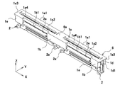
第3実施形態〔図16,図17〕:
前記各実施形態では、1つのコネクタ2に装着されるコネクタ用のキャップ1,5を例示した。これに対し、装着部1eと、挿通孔1a2とを2つずつ有しており、各装着部1eにコネクタ2のハウジング2aを保持するコネクタ用のキャップ6とすることができる。コネクタ用のキャップ6は装着部1eを幅方向Xに沿って2つ設けた構造となっている。そのため、2つのコネクタ2に装着することができる。
Third Embodiment (FIGS. 16 and 17):
In the above embodiments, the
こうしたコネクタ用のキャップ6は、各装着部1e,1eに装着されるコネクタ2,2の挿入口2d1,2d1に合わせて挿通孔1a2を一つずつ形成することで、コネクタ用のキャップ6にコネクタ2,2を装着した状態で、各コネクタ2に2枚の平型導体4を挿入することができる。また、2つのコネクタ2に装着したコネクタ用のキャップ6を吸着ヘッドで吸着し、基板3に実装することで、同時に2つのコネクタ2を基板に固定することができるため、作業効率を向上させることができる。よって、実装作業を減らすことができるため、基板3によるコネクタ2,2の実装位置のばらつきの発生を抑えることができる。さらに、装着部1e,1e同士の間に設けられる連結部6aの長さを基板3上におけるコネクタ2,2の実装位置に合わせてあらかじめ設計しておくことで、コネクタ2,2を互いに一定の間隔を設けた状態で目的位置に実装することができる。なお、コネクタ用のキャップ6は絶縁性樹脂でなるため、コネクタ用のキャップ6を2つのコネクタ2に装着しても互いに絶縁状態を維持することができる。
The
3つ以上のコネクタ2を同時に基板に固定する場合には、それと同じ数の装着部1eを設けることができる。なお、本実施形態のコネクタ用のキャップ6は幅方向Xに沿って2つの装着部1eを設けたが、基板(図示略)に前後方向Yに沿って2つのコネクタ2を固定する場合には、前後方向Yに沿って装着部1eを設けることもできる。ただし、この場合にはコネクタ2のレバー部2eを操作できる配置でコネクタ2,2にコネクタ用のキャップを装着する。また、連結部6aを前後方向Yで長くするなどにより、一方のコネクタ2の端子2bと他方のコネクタ2の端子2bとを離間して配置する。
When three or
また、本実施形態のコネクタ用のキャップ6としては、装着部1eと同数の挿通孔1a2を有する例を示した。これに対して、挿通孔1a2を1つだけ有することとしても良い。この場合には、複数のハウジング2aの挿入口2d1と連通するように、挿通孔1a2を大きく設けることで、1つの挿通孔1a2が複数の平型導体4を挿通し、挿入口2d1までガイドすることができる。
Moreover, as the
1 コネクタ用のキャップ(第1実施形態)
1a カバー部
1a1 吸着面
1a2 挿通孔
1a3 突出部
1a4 誘い込み部
1b 前壁部
1b1 凹部
1c 後壁部
1d 側壁部
1d1 係止部
1d2 係止片部
1d3 係止突起
1e 装着部
2 コネクタ
2a ハウジング
2a1 被係止部
2b 端子
2c グラウンド端子
2d 上壁部
2d1 挿入口
2e レバー部
3 基板
4 平型導体
5 コネクタ用のキャップ(第2実施形態)
5a シャッター部
5b スリット部
6 コネクタ用のキャップ(第3実施形態)
6a 連結部
1 Cap for connector (first embodiment)
1a Cover part 1a1 Adsorption surface 1a2 Insertion hole 1a3 Projection part 1a4 Lead-in
6a Connection
Claims (4)
前記ハウジングに備わる前記コネクタの接続対象物の挿入口に沿って設けられるカバー部とを有しており、
前記カバー部は、前記ハウジングの前記挿入口と連通し、前記接続対象物を挿通する挿通孔を有し、
前記装着部は、前記カバー部から前記コネクタの側面に伸長する側壁部を有するコネクタ用のキャップにおいて、
前記側壁部は、前記カバー部から片持ち梁状に伸長して前記ハウジングの側面に設けた被係止部に対して係止する係止部を有しており、
前記係止部は、前記側壁部の下端位置よりも短い長さで形成されており、
前記側壁部は、前記装着部を前記コネクタに装着する際に、前記係止部以外の部位が前記コネクタの側面と接触した後に、前記係止部が前記コネクタの側面と接触するようにして、前記コネクタに装着されることを特徴とするコネクタ用のキャップ。
A mounting portion for holding the connector housing;
And a cover portion provided along the insertion port of the connection object of the connector provided in the housing,
The cover portion communicates with the insertion port of the housing and has an insertion hole through which the connection object is inserted.
The mounting portion is a cap for a connector having a side wall portion extending from the cover portion to a side surface of the connector,
The side wall portion has a locking portion which extends in a cantilever shape from the cover portion and locks with a locked portion provided on the side surface of the housing.
The locking portion is formed to have a length shorter than the lower end position of the side wall portion,
The side wall portion is configured such that, when the mounting portion is attached to the connector, the locking portion contacts the side surface of the connector after a portion other than the locking portion contacts the side surface of the connector. A cap for a connector mounted on the connector.
前記シャッター部は、前記キャップを形成する絶縁性樹脂にて一体形成された弾性を有する薄膜で形成されている
請求項1記載のコネクタ用のキャップ。
The shutter has a shutter portion that closes the insertion hole in a non-inserted state of the connection object, and is pressed when the connection object is inserted to open the insertion hole.
The cap for a connector according to claim 1, wherein the shutter portion is formed of an elastic thin film integrally formed of an insulating resin forming the cap.
請求項1又は請求項2記載のコネクタ用のキャップ。
The housing has a plurality of mounting parts for holding the housing so as to surround the upper end side of the outer peripheral surface of the housing, and at least one insertion hole provided for each mounting part, each mounting part comprising: The cap for the connector according to claim 1, wherein the housings of the different connectors are held.
請求項1〜請求項3何れか1項記載のコネクタ用のキャップ。
The cap for a connector according to any one of claims 1 to 3, wherein the cover portion has a projecting portion which protrudes to the side of the side wall portion.
Priority Applications (1)
| Application Number | Priority Date | Filing Date | Title |
|---|---|---|---|
| JP2015126551A JP6530976B2 (en) | 2015-06-24 | 2015-06-24 | Connector cap |
Applications Claiming Priority (1)
| Application Number | Priority Date | Filing Date | Title |
|---|---|---|---|
| JP2015126551A JP6530976B2 (en) | 2015-06-24 | 2015-06-24 | Connector cap |
Publications (2)
| Publication Number | Publication Date |
|---|---|
| JP2017010836A JP2017010836A (en) | 2017-01-12 |
| JP6530976B2 true JP6530976B2 (en) | 2019-06-12 |
Family
ID=57764087
Family Applications (1)
| Application Number | Title | Priority Date | Filing Date |
|---|---|---|---|
| JP2015126551A Active JP6530976B2 (en) | 2015-06-24 | 2015-06-24 | Connector cap |
Country Status (1)
| Country | Link |
|---|---|
| JP (1) | JP6530976B2 (en) |
Families Citing this family (1)
| Publication number | Priority date | Publication date | Assignee | Title |
|---|---|---|---|---|
| JP7184996B2 (en) * | 2017-07-11 | 2022-12-06 | イリソ電子工業株式会社 | connector |
Family Cites Families (3)
| Publication number | Priority date | Publication date | Assignee | Title |
|---|---|---|---|---|
| US4795354A (en) * | 1987-09-03 | 1989-01-03 | Gte Products Corporation | Dust cover for printed circuit board card connector |
| US6464537B1 (en) * | 1999-12-29 | 2002-10-15 | Berg Technology, Inc. | High speed card edge connectors |
| JP2015022793A (en) * | 2013-07-16 | 2015-02-02 | ヒロセ電機株式会社 | Cover for connector |
-
2015
- 2015-06-24 JP JP2015126551A patent/JP6530976B2/en active Active
Also Published As
| Publication number | Publication date |
|---|---|
| JP2017010836A (en) | 2017-01-12 |
Similar Documents
| Publication | Publication Date | Title |
|---|---|---|
| JP6342185B2 (en) | connector | |
| JP6254542B2 (en) | Connector device having a cable connector | |
| TWI555277B (en) | Electrical connector | |
| JP2007012396A (en) | Connector for substrate | |
| US20150318639A1 (en) | Lever-type connector | |
| JP2010097727A (en) | Board-to-board connector | |
| JP6689063B2 (en) | connector | |
| JP2015072868A (en) | Connector | |
| US9705251B2 (en) | Lever-type connector | |
| JP5913014B2 (en) | connector | |
| JP6530976B2 (en) | Connector cap | |
| JP2022000864A (en) | Electric connector | |
| US9331428B2 (en) | Connector mateable with mating connector and having lock structure including lock member and operation member which is operable to move lock member | |
| JP4723528B2 (en) | Two-piece connector | |
| JP4346723B2 (en) | Electrical connector | |
| JP7059921B2 (en) | Connector assembly | |
| EP3451806B1 (en) | Method for manufacturing circuit board, circuit board, and cover member | |
| JP2016085812A (en) | Electric connector | |
| JP2008010592A (en) | Jointing structure of substrate | |
| JP7456574B2 (en) | Connector with adsorption member | |
| JP2020092576A (en) | Electric connection box | |
| JP6052084B2 (en) | Electrical junction box | |
| JP6215628B2 (en) | Tine plate and electrical connector | |
| JP2015018623A (en) | Connector | |
| KR200481500Y1 (en) | Connector |
Legal Events
| Date | Code | Title | Description |
|---|---|---|---|
| A621 | Written request for application examination |
Free format text: JAPANESE INTERMEDIATE CODE: A621 Effective date: 20180319 |
|
| A977 | Report on retrieval |
Free format text: JAPANESE INTERMEDIATE CODE: A971007 Effective date: 20181113 |
|
| A131 | Notification of reasons for refusal |
Free format text: JAPANESE INTERMEDIATE CODE: A131 Effective date: 20181120 |
|
| A601 | Written request for extension of time |
Free format text: JAPANESE INTERMEDIATE CODE: A601 Effective date: 20190117 |
|
| A521 | Request for written amendment filed |
Free format text: JAPANESE INTERMEDIATE CODE: A523 Effective date: 20190315 |
|
| TRDD | Decision of grant or rejection written | ||
| A01 | Written decision to grant a patent or to grant a registration (utility model) |
Free format text: JAPANESE INTERMEDIATE CODE: A01 Effective date: 20190514 |
|
| A61 | First payment of annual fees (during grant procedure) |
Free format text: JAPANESE INTERMEDIATE CODE: A61 Effective date: 20190520 |
|
| R150 | Certificate of patent or registration of utility model |
Ref document number: 6530976 Country of ref document: JP Free format text: JAPANESE INTERMEDIATE CODE: R150 |
|
| R250 | Receipt of annual fees |
Free format text: JAPANESE INTERMEDIATE CODE: R250 |
|
| R250 | Receipt of annual fees |
Free format text: JAPANESE INTERMEDIATE CODE: R250 |