JP6523873B2 - Method of manufacturing mask blank, method of manufacturing transfer mask, and mask blank - Google Patents
Method of manufacturing mask blank, method of manufacturing transfer mask, and mask blank Download PDFInfo
- Publication number
- JP6523873B2 JP6523873B2 JP2015167664A JP2015167664A JP6523873B2 JP 6523873 B2 JP6523873 B2 JP 6523873B2 JP 2015167664 A JP2015167664 A JP 2015167664A JP 2015167664 A JP2015167664 A JP 2015167664A JP 6523873 B2 JP6523873 B2 JP 6523873B2
- Authority
- JP
- Japan
- Prior art keywords
- film
- mask
- hard mask
- manufacturing
- mask blank
- Prior art date
- Legal status (The legal status is an assumption and is not a legal conclusion. Google has not performed a legal analysis and makes no representation as to the accuracy of the status listed.)
- Active
Links
Images


Description
本発明は、マスクブランクの製造方法、転写用マスクの製造方法、およびマスクブランクに関する。 The present invention relates to a method of manufacturing a mask blank, a method of manufacturing a transfer mask, and a mask blank.
マスクブランクにおいて基板上に設けられた薄膜の中には、その最表面にケイ素化合物からなるハードマスク膜を有するものがある。ケイ素化合物からなる薄膜は、塩素系ガスに対するドライエッチング耐性に優れることから、遮光膜として用いられるクロム系薄膜等を塩素系ガスでドライエッチングする場合のマスクパターンとして有用である。また、厚さ5nm以下のきわめて薄膜であってもマスクとして機能を果たすことから、ハードマスク膜をエッチングする際にマスクとして用いるレジスト膜を薄膜化することができる。これにより、基板上の薄膜に対して、100nm以下の寸法の微細パターンを転写することが可能となる。 Among thin films provided on a substrate in a mask blank, there is one having a hard mask film made of a silicon compound on the outermost surface thereof. Since a thin film made of a silicon compound is excellent in dry etching resistance to a chlorine gas, it is useful as a mask pattern when dry etching a chromium thin film or the like used as a light shielding film with a chlorine gas. Further, even a very thin film having a thickness of 5 nm or less can function as a mask, so that the resist film used as a mask when etching the hard mask film can be thinned. This makes it possible to transfer a fine pattern of a dimension of 100 nm or less to the thin film on the substrate.
ここで、ケイ素系化合物からなるハードマスク膜の表面は極性表面であり、極性の低い有機化合物からなるレジスト膜に対する密着性が十分ではない。このため、例えば線幅50nm以下の微細パターンの形成においては、リソグラフィーによってレジスト膜に形成したレジストパターンのパターン倒れが発生する。そこでマスクブランクの製造工程においては、薄膜の上部にレジスト膜を形成する前に、ハードマスク膜の表面に対して密着性改善のための表面改質処理が行われている。この表面改質処理においては、例えばハードマスク膜に対して例えば窒素ガスを用いて蒸散させたHMDS(ヘキサメチルジシラザン)を接触させ、ハードマスク膜の表面にごく薄い疎水性表面層を形成する(例えば下記特許文献1参照)。 Here, the surface of the hard mask film made of a silicon-based compound is a polar surface, and adhesion to a resist film made of an organic compound with a low polarity is not sufficient. For this reason, for example, in the formation of a fine pattern having a line width of 50 nm or less, pattern collapse of a resist pattern formed on a resist film by lithography occurs. Therefore, in the manufacturing process of the mask blank, before forming the resist film on the top of the thin film, the surface modification treatment for improving the adhesion to the surface of the hard mask film is performed. In this surface modification treatment, for example, HMDS (hexamethyldisilazane) evaporated by using, for example, nitrogen gas is brought into contact with the hard mask film to form a very thin hydrophobic surface layer on the surface of the hard mask film. (For example, refer to the following patent document 1).
ところで、マスクブランクを用いた転写用マスクの製造においては、レジスト膜のリソグラフィー処理によってレジストパターンを形成した後には、速やかに当該レジストパターンをマスクにして下層のハードマスク膜をエッチングすることが好ましい。これにより、レジストパターンに異物が付着することによる下層のエッチング形状の劣化が防止されるためである。 By the way, in the manufacture of a transfer mask using a mask blank, after forming a resist pattern by lithography processing of a resist film, it is preferable to rapidly etch the lower hard mask film by using the resist pattern as a mask. This is because deterioration of the etching shape of the lower layer due to the adhesion of foreign matter to the resist pattern is prevented.
しかしながら、レジストパターン形成後、直ちに下層のハードマスク膜をエッチングした場合であっても、ハードマスクパターンに欠陥が発生する現象が生じた。 However, even when the underlying hard mask film is etched immediately after forming the resist pattern, a phenomenon occurs in which a defect occurs in the hard mask pattern.
そこで本発明は、レジストパターン形成直後であってもケイ素系化合物を用いて構成されたハードマスク膜を高精度にパターニングすることが可能なマスクブランクの製造方法を提供すること、および形状精度の良好な微細パターンを有する転写用マスクの製造方法を提供することを目的とする。 Therefore, the present invention provides a method of manufacturing a mask blank capable of patterning a hard mask film formed using a silicon-based compound with high accuracy even immediately after resist pattern formation, and having a good shape accuracy. It is an object of the present invention to provide a method of manufacturing a transfer mask having a fine pattern.
<構成1>
基板上に、パターニング材料膜と、ケイ素を含有するハードマスク膜とをこの順に成膜する成膜工程と、
有機ケイ素化合物を用いた処理により、前記ハードマスク膜の表面のシラノール基を化学修飾基で修飾する改質処理工程と、
前記改質処理された前記ハードマスク膜上にレジスト膜を形成する工程とを有し、
前記改質処理は、室温23℃における前記ハードマスク膜の表面の水接触角が40°以上55°以下の範囲となるように行う
マスクブランクの製造方法。
<Configuration 1>
Forming a patterning material film and a hard mask film containing silicon on the substrate in this order;
A modification treatment step of modifying silanol groups on the surface of the hard mask film with a chemical modification group by treatment using an organosilicon compound;
Forming a resist film on the modified hard mask film;
The method for manufacturing a mask blank, wherein the modification treatment is performed such that a water contact angle on the surface of the hard mask film at a room temperature of 23 ° C. is in a range of 40 ° to 55 °.
<構成2>
基板上に、パターニング材料膜と、ケイ素を含有するハードマスク膜とをこの順に成膜する成膜工程と、
有機ケイ素化合物を用いた処理により、前記ハードマスク膜の表面のシラノール基を化学修飾基で修飾する改質処理工程と、
前記改質処理された前記ハードマスク膜上にレジスト膜を形成する工程とを有し、
前記改質処理は、前記シラノール基の前記化学修飾基による被覆率が、飽和被覆率を100%とした場合に45%以上85%以下の範囲となるように処理を行う
マスクブランクの製造方法。
<
Forming a patterning material film and a hard mask film containing silicon on the substrate in this order;
A modification treatment step of modifying silanol groups on the surface of the hard mask film with a chemical modification group by treatment using an organosilicon compound;
Forming a resist film on the modified hard mask film;
The method for manufacturing a mask blank, wherein the modification treatment is performed such that the coverage by the chemical modification group of the silanol group is in the range of 45% to 85% when the saturation coverage is 100%.
<構成3>
前記成膜工程では、前記パターニング材料膜として、クロムを含有する材料膜を成膜する
ことを特徴とする構成1または2記載のマスクブランクの製造方法。
<Configuration 3>
In the film forming step, a material film containing chromium is formed as the patterning material film. The method for manufacturing a mask blank according to
<構成4>
前記有機ケイ素化合物は、アミンを有している
ことを特徴とする構成1〜3の何れかに記載のマスクブランクの製造方法。
<Configuration 4>
The method for producing a mask blank according to any one of constitutions 1 to 3, wherein the organic silicon compound has an amine.
<構成5>
前記有機ケイ素化合物は、ヘキサメチルジシラザンである
ことを特徴とする構成1〜4の何れかに記載のマスクブランクの製造方法。
<Configuration 5>
7. The method for producing a mask blank according to any one of constitutions 1 to 4, wherein the organosilicon compound is hexamethyldisilazane.
<構成6>
前記ハードマスク膜の膜厚は、1.5nm以上15nm未満である
ことを特徴とする構成1〜5の何れかに記載のマスクブランクの製造方法。
<Configuration 6>
7. The method for producing a mask blank according to any one of constitutions 1 to 5, wherein the film thickness of the hard mask film is 1.5 nm or more and less than 15 nm.
<構成7>
前記ハードマスク膜は、酸素および窒素のうちの少なくとも一方とケイ素とからなる
ことを特徴とする構成1〜6の何れかに記載のマスクブランクの製造方法。
<Configuration 7>
7. The method for producing a mask blank according to any one of the constitutions 1 to 6, wherein the hard mask film comprises silicon and at least one of oxygen and nitrogen.
<構成8>
構成1〜7の何れかに記載のマスクブランクの製造方法によって製造されたマスクブランクを用いる転写用マスクの製造方法であって、
リソグラフィー法により前記レジスト膜にレジストパターンを形成する工程と、
前記レジストパターンをマスクとし、フッ素系ガスを用いたドライエッチングにより、前記ハードマスク膜をパターニングする工程と、
前記パターニングされたハードマスク膜をマスクとして前記パターニング材料膜をエッチングすることにより、当該パターニング材料膜をパターニングする工程とを有する
転写用マスクの製造方法。
<Configuration 8>
A method for producing a transfer mask using a mask blank produced by the method for producing a mask blank according to any one of constitutions 1 to 7, comprising:
Forming a resist pattern on the resist film by a lithography method;
Patterning the hard mask film by dry etching using a fluorine-based gas using the resist pattern as a mask;
And D. the step of patterning the patterning material film by etching the patterning material film using the patterned hard mask film as a mask.
<構成9>
前記成膜工程では、前記パターニング材料膜として、クロムを含有する材料膜を成膜し、
前記パターニング材料膜をパターニングする工程では、前記ハードマスク膜をマスクとし、塩素系ガスを用いたドライエッチングより、前記クロムを含有する材料膜をパターニングする
ことを特徴とする構成8記載の転写用マスクの製造方法。
<Configuration 9>
In the film forming step, a material film containing chromium is formed as the patterning material film,
In the step of patterning the patterning material film, the hard mask film is used as a mask, and the chromium-containing material film is patterned by dry etching using a chlorine-based gas. Manufacturing method.
<構成10>
基板上に、パターニング材料膜と、ケイ素を含有するハードマスク膜とがこの順で成膜されたマスクブランクであって、
前記ハードマスク膜は、有機ケイ素化合物を用いた処理によって、表面のシラノール基が化学修飾基で修飾されており、修飾された表面の水接触角が40°以上55°未満である
ことを特徴とするマスクブランク。
<
A mask blank in which a patterning material film and a hard mask film containing silicon are formed in this order on a substrate,
The hard mask film is characterized in that the surface silanol group is modified with a chemical modification group by treatment with an organosilicon compound, and the water contact angle of the modified surface is 40 ° or more and less than 55 °. Mask blank.
<構成11>
基板上に、パターニング材料膜と、ケイ素を含有するハードマスク膜とがこの順で成膜されたマスクブランクであってり、
前記ハードマスク膜は、有機ケイ素化合物を用いた処理によって、表面のシラノール基が化学修飾基で修飾されており、修飾された表面の前記化学修飾基による被覆率が飽和被覆率を100%とした場合に45%以上85%以下である
ことを特徴とするマスクブランク。
<
It is a mask blank on which a patterning material film and a hard mask film containing silicon are formed in this order on a substrate,
In the hard mask film, the silanol group on the surface is modified with a chemical modifying group by treatment with an organosilicon compound, and the coverage of the modified surface with the chemical modifying group is 100% saturated coverage. In some cases, the mask blank is 45% or more and 85% or less.
以上の構成を有する本発明の製造方法によれば、レジスト膜とケイ素系化合物を用いて構成されたハードマスク膜との密着性を確保しつつ、レジストパターン形成直後であってもハードマスク膜を高精度にパターニングすることが可能なマスクブランクを得ることが可能である。またこの製造方法によって得られたマスクブランクを用いることにより、形状精度の良好な微細パターンを有する転写用マスクを得ることが可能になる。 According to the manufacturing method of the present invention having the above configuration, the hard mask film can be formed immediately after the formation of the resist pattern while securing the adhesion between the resist film and the hard mask film formed using the silicon compound. It is possible to obtain a mask blank that can be patterned with high accuracy. In addition, by using the mask blank obtained by this manufacturing method, it becomes possible to obtain a transfer mask having a fine pattern with good shape accuracy.
発明者らは、ケイ素系化合物からなるハードマスク膜上にレジスト膜が設けられた構成のマスクブランクに関し、リソグラフィーの直後に直ちに下層のハードマスク膜をパターンエッチングしてハードマスクパターンを形成した場合に、ハードマスクパターンに生じる欠陥の発生原因について検討を行った。 The inventors have dealt with a mask blank having a configuration in which a resist film is provided on a hard mask film made of a silicon-based compound, and immediately after lithography, the hard mask film is formed by pattern etching the lower hard mask film immediately. The cause of defects generated in the hard mask pattern was examined.
その結果、欠陥の形成分布と、リソグラフィー処理によるレジストパターン形成後に処理表面に残存している水滴の分布とが類似していることを突き止めた。そしてこのことから、レジストパターンをマスクにしてハードマスク膜をドライエッチングする際の減圧処理に伴う低温化の影響で、処理表面に残存している水滴が氷化し、その氷がマスクとなってハードマスク膜のエッチングを阻害していると推測した。詳しく説明すると、次のとおりである。 As a result, it was found that the distribution of formation of defects was similar to the distribution of water droplets remaining on the treated surface after resist pattern formation by lithography processing. From this fact, the water droplets remaining on the treated surface become iced due to the influence of temperature reduction accompanying the pressure reduction processing when dry etching the hard mask film using the resist pattern as a mask, and the ice functions as a mask It was presumed that the etching of the mask film was inhibited. The details are as follows.
すなわち、リソグラフィー処理によるレジストパターン形成においては、現像・リンス処理後に、処理表面をスピン乾燥する。この際、処理表面にはレジストパターンによる凹凸が形成されているため、微細な水滴がレジストパターン間に残存する。レジストパターン間には、表面改質処理によってごく薄い疎水性表面層が形成されたハードマスク膜の表面が露出した状態となっている。このため、レジストパターン間に残存する水滴は、ハードマスク膜に対して大きな接触角で盛り上がり、体積に対して表面積が小さい形状となっている。 That is, in the resist pattern formation by the lithography process, the processing surface is spin-dried after the development and rinse process. Under the present circumstances, since the unevenness | corrugation by a resist pattern is formed in the process surface, a fine water droplet remains between resist patterns. Between the resist patterns, the surface of the hard mask film on which a very thin hydrophobic surface layer is formed by surface modification treatment is exposed. For this reason, the water droplets remaining between the resist patterns are raised at a large contact angle with respect to the hard mask film, and the surface area is smaller than the volume.
ここでリソグラフィー処理によるレジストパターン形成の直後、すなわちスピン乾燥の直後にドライエッチングのための減圧処理を施した場合、平らな形状に付着した水滴であれば、体積に対する表面積が大きいため減圧環境下で容易に蒸発する。これに対して、大きな接触角で盛り上がった形状の水滴は、表面積が小さいために蒸発効率が悪く、減圧に伴うチャンバー内空間の温度低下と水滴表面からの気化熱により急冷されることによって凝固(氷化)し、その氷がハードマスク膜のエッチングの際の異物要素になっていると推測した。 Here, when a reduced pressure treatment for dry etching is performed immediately after formation of a resist pattern by lithography processing, that is, immediately after spin drying, if the water droplet adheres to a flat shape, the surface area with respect to volume is large under a reduced pressure environment. Evaporate easily. On the other hand, water droplets that swell in large contact angles have poor evaporation efficiency because they have a small surface area, and are solidified by being quenched by the temperature drop in the chamber interior due to pressure reduction and the heat of vaporization from the surface of the water droplets ( It was iced, and it was inferred that the ice was a foreign matter component in the etching of the hard mask film.
そこで発明者らは、ケイ素系化合物を用いて構成されたハードマスク膜上にレジスト膜を形成する場合のハードマスク膜の表面改質処理として、単なる疎水化処理ではなく、レジスト膜との密着性を確保しつつも、リソグラフィー処理の後に残存する水滴に有る程度の蒸発(蒸散)効率が得られる範囲の親水性とする処理を行うことにより、上述した欠陥の発生を防止できるという結論に至った。 Therefore, the present inventors are not mere hydrophobic treatment as the surface modification treatment of the hard mask film in the case of forming the resist film on the hard mask film configured using a silicon compound, and the adhesion to the resist film It has been concluded that the above-mentioned defects can be prevented by performing the treatment to make the water droplets remaining after the lithography process have a certain degree of evaporation (transpiration) efficiency while maintaining the .
以下に、上述した効果を得るための本発明の詳細な構成を、図面に基づいて説明する。ここでは、本発明を位相シフト型のマスクブランクの製造方法に適用した実施の形態を説明し、次いでこの製造方法によって得られたマスクブランクを用いた転写用マスクの製造方法の実施の形態を説明する。尚、各図において同様の構成要素には同一の符号を付して説明を行う。 Hereinafter, the detailed configuration of the present invention for obtaining the above-described effects will be described based on the drawings. Here, an embodiment in which the present invention is applied to a method of manufacturing a phase-shifting mask blank will be described, and then an embodiment of a method of manufacturing a transfer mask using the mask blank obtained by this manufacturing method will be described. Do. In the drawings, the same components are denoted by the same reference numerals.
≪マスクブランクの製造方法≫
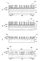
図1は、実施形態のマスクブランクの製造方法を説明するための断面工程図である。以下に、図1に基づき、実施形態のマスクブランクの製造方法を説明する。
«Method of manufacturing mask blank»
FIG. 1 is a cross-sectional process drawing for explaining the manufacturing method of the mask blank of the embodiment. Below, based on FIG. 1, the manufacturing method of the mask blank of embodiment is demonstrated.
先ず図1Aに示すように、基板10を用意し、この基板10上に、ハーフトーン膜11、遮光膜13、およびケイ素系材料からなるハードマスク膜15をこの順に成膜する成膜工程を行う。このうちハーフトーン膜11および遮光膜13は、微細なパターンが転写形成されるパターニング材料膜として成膜される。また遮光膜13は、クロムを含有する材料膜として成膜される。次に、各構成要素およびその成膜手順の詳細を説明する。
First, as shown in FIG. 1A, a
<基板10>
ここで用意する基板10は、一般的にガラス材から構成され、ケイ素を含有する材料からなるものが選択される。例えばバイナリマスクや位相シフトマスク用のマスクブランクの基板1であれば、ArFエキシマレーザ光(波長:約193nm)のような露光光に対して透過性を有する材料で構成されればよい。このような材料としては、合成石英ガラスが用いられるが、この他にも、アルミノシリケートガラス、ソーダライムガラスを用いることができる。特に、石英基板は、ArFエキシマレーザ光、またはそれよりも短波長の領域で透明性が高いので、本発明のマスクブランクに特に好適に用いることができる。
また、反射型のマスクブランクの基板1であれば、露光時の発熱による熱膨張が低く抑えられた低熱膨張ガラス(SiO2−TiO2ガラス等)を用いて構成される。
<
The
Further, if the substrate 1 of the reflective mask blank, constituted by a thermal expansion due to heat generation during exposure is kept low to low thermal expansion glass (SiO 2 -TiO 2 glass).
以上のような基板10は、周端面および主表面が所定の表面粗さに研磨され、その後、所定の洗浄処理および乾燥処理が施されたものである。
In the
尚、ここで言うリソグラフィーにおける露光工程とは、マスクブランクを用いて作製された転写用マスクを用いてのリソグラフィーにおける露光工程であり、以下において露光光とはこの露光工程で用いられる露光光であることとする。転写用マスクがバイナリマスクや位相シフトマスクの場合、この露光光としては、ArFエキシマレーザ光(波長:193nm)、KrFエキシマレーザ光(波長:248nm)、i線光(波長:365nm)のいずれも適用可能であるが、露光工程における位相シフトパターンの微細化の観点からは、ArFエキシマレーザ光を露光光に適用することが望ましい。また転写用マスクが反射型マスクである場合、この露光光としては、EUV光(波長:13.56nm)が適用される。 Here, the exposure step in lithography referred to herein is an exposure step in lithography using a transfer mask manufactured using a mask blank, and in the following, exposure light is exposure light used in this exposure step. To be. When the transfer mask is a binary mask or a phase shift mask, any of ArF excimer laser light (wavelength: 193 nm), KrF excimer laser light (wavelength: 248 nm) and i-line light (wavelength: 365 nm) can be used as this exposure light. Although applicable, it is desirable to apply ArF excimer laser light to the exposure light from the viewpoint of miniaturization of the phase shift pattern in the exposure process. When the transfer mask is a reflective mask, EUV light (wavelength: 13.56 nm) is applied as the exposure light.
<ハーフトーン膜11の成膜>
次に、以上のような基板10における処理表面上に、例えばスパッタ法によってハーフトーン膜11を成膜する。ここで成膜するハーフトーン膜11は、例えばケイ素(Si)を含有する材料膜として成膜する。このハーフトーン膜11は、ケイ素の他に、窒素(N)を含有する材料で形成されていることが好ましい。このようなハーフトーン膜11は、フッ素系ガスを用いたドライエッチングによってパターニングが可能であり、以下に説明するクロム(Cr)を含有する材料で形成された遮光膜13に対して、十分なエッチング選択性を有したパターニングが可能である。
<Formation of
Next, the
またハーフトーン膜11は、フッ素系ガスを用いたドライエッチングによってパターニングが可能であれば、さらに、半金属元素、非金属元素、金属元素から選ばれる1以上の元素を含有していてもよい。
The
このうち、半金属元素は、ケイ素に加え、いずれの半金属元素であってもよい。非金属元素は、窒素に加え、いずれの非金属元素であっても良く、例えば酸素(O)、炭素(C)、フッ素(F)および水素(H)から選ばれる一以上の元素を含有させると好ましい。また金属元素は、モリブデン(Mo)、タングステン(W)、チタン(Ti)、タンタル(Ta)、ジルコニウム(Zr)、ハフニウム(Hf)、ニオブ(Nb)、バナジウム(V)、コバルト(Co)、クロム(Cr)、ニッケル(Ni)、ルテニウム(Ru)、スズ(Sn)、ホウ素(B)、ゲルマニウム(Ge)が例示される。 Among these, the metalloid element may be any metalloid element in addition to silicon. The nonmetallic element may be any nonmetallic element in addition to nitrogen, and for example, it contains one or more elements selected from oxygen (O), carbon (C), fluorine (F) and hydrogen (H) Preferred. In addition, metal elements include molybdenum (Mo), tungsten (W), titanium (Ti), tantalum (Ta), zirconium (Zr), hafnium (Hf), niobium (Nb), vanadium (V), cobalt (Co), Chromium (Cr), nickel (Ni), ruthenium (Ru), tin (Sn), boron (B) and germanium (Ge) are exemplified.
このような元素を含有するハーフトーン膜11として、例えばMoSiNで構成されたものが例示される。
As the
またハーフトーン膜11は、露光光に対して所定の位相差と所定の透過率となるように、屈折率n、消衰係数k、および膜厚が設定され、その屈折率nおよび消衰係数kとなるように、膜材料の組成や成膜条件を調整して成膜される。一例として、露光光がArFエキシマレーザ光である場合、位相差は例えば150[deg]〜180[deg]であり、透過率は1%〜30%である。
The refractive index n, the extinction coefficient k, and the film thickness are set so that the
またスパッタ法によるハーフトーン膜11の成膜においては、ハーフトーン膜11を構成する材料を所定の組成比で含有するスパッタリングターゲットおよびスパッタガスを用い、さらには必要に応じてアルゴン(Ar)およびヘリウム(He)等の不活性ガスをスパッタガスとして用いた成膜が行われる。
Further, in the film formation of the
スパッタ法によってハーフトーン膜11を成膜した後には、後処理として所定の加熱温度でのアニール処理を行う。
After the
<遮光膜13の成膜>
次に、ハーフトーン膜11上に、例えばスパッタ法によって遮光膜13を成膜する。遮光膜13は、ここで成膜する遮光膜13は、クロムを含有する材料膜であって、単層で成膜してもよく、図示したような下層13aと上層13bとの2層構造で成膜してもよく、さらに多層の複数層で成膜してもよい。遮光膜13を複数層として成膜する場合には、クロム(Cr)の含有量を変化させた各層を成膜する。
<Deposition of
Next, the
ここでクロム系薄膜は、パターニングの際のエッチングガスに塩素を主体とした酸素との混合ガスを使用するが、次に成膜するケイ素系材料からなるハードマスク膜15は塩素系ガスに対して強靭なエッチング耐性を有する。このため、ケイ素系材料からなるハードマスク膜15をマスクにして、クロム系薄膜によって構成された遮光膜13をエッチングする際には、高いエッチング選択性でパターニングエッチングが可能である。
Here, as the chromium-based thin film, a mixed gas of oxygen mainly containing chlorine is used as an etching gas at the time of patterning, but the
また遮光膜13は、クロム金属のほか、クロムに酸素、窒素、炭素、ホウ素、水素およびフッ素から選ばれる一以上の元素を含有する材料を含有していてもよい。さらにこの遮光膜13には、光学濃度(OD)を維持しつつも、膜全体のエッチングレートの低下を抑制することを目的として、インジウム(In)、スズ(Sn)、およびモリブデン(Mo)から選ばれる少なくとも1以上の金属元素(インジウム等金属元素)を含有していてもよい。
The
このような遮光膜13は、酸素含有塩素系ガスを用いたドライエッチングによってパターニングが可能である。また、この遮光膜13はケイ素(Si)を含有する材料で形成されたハーフトーン膜11との間で十分なエッチング選択性を有しており、ハーフトーン膜11にほとんどダメージを与えずに遮光膜13をエッチング除去することが可能である。この遮光膜13は、以下に説明するケイ素(Si)を含有する材料で形成されたハードマスク膜15に対して十分なエッチング選択性を有しており、このハードマスク膜15をマスクとした遮光膜13のパターニングが可能である。
Such a
また以上のような遮光膜13は、ドライエッチングにおいての形状精度が確保され、かつ露光転写工程で用いられる露光光に対して所定値以上の光学濃度(OD)を有するように、各層の組成や膜厚が設定して成膜される。
The
スパッタ法による遮光膜13の成膜においては、遮光膜13の各層を構成する材料を所定の組成比で含有するスパッタリングターゲットおよびスパッタガスを用い、さらには必要に応じてアルゴン(Ar)およびヘリウム(He)等の不活性ガスをスパッタガスとして用いた成膜が行われる。
In the formation of the
<ハードマスク膜15の成膜>
次いで遮光膜13上に、例えばスパッタ法によってハードマスク膜15を成膜する。ここで成膜するハードマスク膜15は、ケイ素(Si)を含有する膜であって、遮光膜13にパターンを形成するためのドライエッチングが終わるまでの間、エッチングマスクとして機能するだけの極薄い膜厚を有して成膜される。
<Deposition of
Next, a
このようなハードマスク膜15は、ケイ素(Si)の他に、酸素(O)、窒素(N)、炭素(C)、ホウ素(B)および水素(H)から選らばれる1以上の元素を含有する材料を用いて成膜される。
Such
このうち、ここではケイ素(Si)と共に、酸素(O)および窒素(N)のうちの少なくとも一方からなるハードマスク膜15を成膜することが好ましい。ここのようなハードマスク膜15を構成する材料の具体例としては、酸化シリコン(SiO2)、窒化シリコン(SiN)、酸化窒化シリコン(SiON)等が挙げられる。これらの材料からなるハードマスク膜15は、クロム(Cr)を含有する材料で形成された遮光膜13との間で十分なエッチング選択比を有しており、しかも遮光膜13にほとんどダメージを与えずに、ハードマスク膜15をエッチング除去することが可能である。
Among these, it is preferable to form a
またこれらの材料からなるハードマスク膜15は、下層のクロム(Cr)を含有する材料で形成された遮光膜13との間で十分なエッチング選択比を有しているため、極薄膜であっても十分にエッチングマスクとして機能する。このため、1.5nm〜15nm未満の膜厚で成膜されることとする。
In addition, since the
またスパッタ法によるハードマスク膜15の成膜においては、ハードマスク膜15を構成する材料を所定の組成比で含有するスパッタリングターゲットおよびスパッタガスを用い、さらには必要に応じてアルゴン(Ar)およびヘリウム(He)等の不活性ガスをスパッタガスとして用いた成膜が行われる。
Further, in the formation of the
ここで成膜されたハードマスク膜15の表面Sは、ハードマスク膜15を構成するケイ素(Si)に対してヒドロキシル基(−OH)が結合したシラノール基で覆われ、これによって親水性表面となっている。
The surface S of the
<改質処理工程>
次に、図1Bに示すように、有機ケイ素化合物を用いた処理により、ハードマスク膜15の表面Sのシラノール基を化学修飾基で修飾する改質処理工程を行う。この改質処理工程は、ハードマスク膜15の表面Sの水接触角が、室温23℃において40°以上55°以下となるように実施するところが重要である。
<Reforming treatment process>
Next, as shown in FIG. 1B, a modification treatment step of modifying the silanol group on the surface S of the
改質処理工程で用いられる有機ケイ素化合物は、ハードマスク膜15の表面Sのシラノール基(−SiOH)と結合可能な官能基と、次の工程で形成するレジスト膜との親和性に優れる疎水性の官能基とを有する化合物である。
The organosilicon compound used in the modification treatment step is hydrophobic which is excellent in the affinity between the functional group capable of binding to the silanol group (-SiOH) on the surface S of the
シラノール基(−SiOH)と結合可能な官能基としては、例えば、アミノ基、ヒドロキシル基、クロライド基などが挙げられ、アミノ基、ヒドロキシル基が好ましく例示される。 As a functional group which can be combined with a silanol group (-SiOH), an amino group, a hydroxyl group, a chloride group etc. are mentioned, for example, An amino group and a hydroxyl group are illustrated preferably.
レジスト膜との親和性に優れる官能基としては、レジスト膜を構成するレジスト材料がいかなる成分であるかに応じて適宜決定することができ、例えばレジスト材料と共有結合または水素結合のような化学結合する官能基、または疎水―疎水相互作用等によって結合する官能基が選択される。 The functional group having an excellent affinity to the resist film can be appropriately determined depending on what component the resist material constituting the resist film is, for example, a chemical bond such as a covalent bond or a hydrogen bond with the resist material Functional groups or functional groups to be linked by hydrophobic-hydrophobic interaction and the like are selected.
例えば、レジスト材料と化学結合する官能基としては、アルキルスルフォン酸基、アルキルアミン基、アルキルカルボン酸基が例示される。またレジスト材料と、疎水―疎水相互作用によって結合する官能基としてはアルキル基が例示される。 For example, as a functional group chemically bonded to the resist material, an alkylsulfonic acid group, an alkylamine group, and an alkylcarboxylic acid group are exemplified. Further, an alkyl group is exemplified as a functional group to be bonded to the resist material by the hydrophobic-hydrophobic interaction.
以上のような官能基を備えた有機ケイ素化合物の具体例としては、1,1,3,3−テトラメチルジシラザン、ヘキサメチルジシラザン(HMDS)、ビニルトリメチルシラン、ヘキサメチルジシラン、メチルシラン、ジメチルシラン、トリメチルシラン、ジエチルシラン、プロピルシラン、フェニルシラン、ビニルトリエトキシシラン、テトラメトキシシラン、フェニルトリエトキシシラン、メチルトリエトキシシラン、オクタメチルシクロテトラシロキサン等が挙げられる。 Specific examples of the organosilicon compounds having the above functional groups include 1,1,3,3-tetramethyldisilazane, hexamethyldisilazane (HMDS), vinyltrimethylsilane, hexamethyldisilane, methylsilane, and dimethyl Silane, trimethylsilane, diethylsilane, propylsilane, phenylsilane, vinyltriethoxysilane, tetramethoxysilane, phenyltriethoxysilane, methyltriethoxysilane, octamethylcyclotetrasiloxane and the like can be mentioned.
また、これらの有機ケイ素化合物の中でも、ヘキサメチルジシラザン(HMDS)が好ましく用いられる。ヘキサメチルジシラザン(HMDS)は、トリメチルシリル基[−Si(CH3)3]で置換されたアミン化合物であり、ハードマスク膜15の表面Sのシラノール基(−SiOH)に結合可能な官能基としてアミノ基を有し、レジスト膜との親和性に優れる官能基としてレジスト材料と疎水―疎水相互作用によって結合するメチル基を有する。
Further, among these organic silicon compounds, hexamethyldisilazane (HMDS) is preferably used. Hexamethyldisilazane (HMDS) is an amine compound substituted with a trimethylsilyl group [-Si (CH3) 3], and amino as a functional group capable of binding to a silanol group (-SiOH) on the surface S of the
このようなヘキサメチルジシラザン(HMDS)を用いた改質処理工程によれば、ハードマスク膜15の表面Sのシラノール基(−SiOH)と、ヘキサメチルジシラザン(HMDS)とが反応し、シラノール基(−SiOH)に対して、ヘキサメチルジシラザン(HMDS)のトリメチルシリル基[−Si(CH3)3]が化学修飾基として結合する。これにより、もともとケイ素(Si)を含有するハードマスク膜15の表面にトリメチルシリル基[−Si(CH3)3]が結合する。このため、疎水化度以外の膜質をほとんど変化させることのなくハードマスク膜15の表面の改質処理が施される。このような改質処理は、ケイ素を含有する材料からなる基板10において、ヘキサメチルジシラザン(HMDS)が供給された面も同様に進行する。また、この反応により、発生するアンモニアは、アンモニアガスとして速やかに排出される。
According to the modification process step using such hexamethyldisilazane (HMDS), the silanol group (-SiOH) on the surface S of the
以上のような有機ケイ素化合物を用いた改質処理工程は、ハードマスク膜15の表面Sに対して、有機ケイ素化合物を供給することによって行われる。
The modification process step using the organosilicon compound as described above is performed by supplying the organosilicon compound to the surface S of the
このような改質処理工程は、処理時間、ハードマスク膜15の表面Sに対する有機ケイ素化合物の供給流量、および処理温度のうちの少なくとも1つを制御することにより、シラノール基に対する化学修飾基の結合量を調整する。これにより、ハードマスク膜15の表面Sの水接触角を、室温23℃において40°以上55°以下の範囲とする。またこの改質処理工程、シラノール基に対する化学修飾基による被覆率を、飽和被覆率を100%とした場合に45%以上85%以下の範囲として実施してもよい。尚、水接触角の測定は、接触角計によって測定することができる。また化学修飾基による被覆率は、化学修飾基のイオン等を直接的または間接的に測定できる質量分析装置(例えばTOF−SIMS)によって測定することができる。
Such a modification treatment step includes bonding of a chemical modification group to a silanol group by controlling at least one of a treatment time, a supply flow rate of an organosilicon compound to the surface S of the
<レジスト膜17の成膜>
次に図1Cに示すように、化学修飾基の結合によって改質処理されたハードマスク膜15の表面S上に、レジスト膜17を形成する。レジスト膜17の形成は、例えばスピンコート法のような塗布法によるレジスト材料層の成膜と、その後の処理とを行う。ここで形成するレジスト膜17は、特に材料限定されることはないが、微細パターンを形成する場合に有効であるため、化学増幅型レジストに適用することが好ましい。また、ネガ型、ポジ型のいずれのレジストにも適用可能であるが、ネガ型に適用すると効果的である。
<Deposition of Resist
Next, as shown in FIG. 1C, a resist
以上により、基板10上に、ハーフトーン膜11、遮光膜13、ハードマスク膜15、およびレジスト膜17をこの順に積層したマスクブランク1が得られる。
Thus, the mask blank 1 in which the
≪転写用マスクの製造方法≫
図2および図3は、実施形態の転写用マスクの製造方法を説明するための断面工程図である。これらの図に示す転写用マスクの製造方法は、図1を用いて説明した製造方法によって得られたハーフトーン型のマスクブランク1を用いた転写用マスクの製造方法である。以下に、図2および図3に基づき、転写用マスクの製造方法を説明する。尚、図2および図3においては、図1を用いて説明した構成要素と同一の構成要素には同一の符号を付し、重複する説明は省略する。
«Method of manufacturing transfer mask»
FIG. 2 and FIG. 3 are cross-sectional process drawings for explaining the manufacturing method of the transfer mask of the embodiment. The method for producing a transfer mask shown in these figures is a method for producing a transfer mask using the halftone mask blank 1 obtained by the production method described with reference to FIG. Hereinafter, a method of manufacturing a transfer mask will be described with reference to FIGS. 2 and 3. In FIG. 2 and FIG. 3, the same components as those described with reference to FIG.
<レジストパターンの形成>
先ず、図2Aに示すように、リソグラフィー法によりレジスト膜17に第1のレジストパターン17aを形成する。ここでは先ず、マスクブランク1におけるレジスト膜17に対して、ハーフトーン膜11に形成すべき位相シフトパターンとアライメントマークパターンとを露光描画する。この露光描画には、電子線が用いられる場合が多い。この際、基板10における中央部分を位相シフトパターン形成領域10aとし、ここに位相シフトパターンに対応するパターンを露光描画する。また、位相シフトパターン形成領域10aの外周領域10bには、位相シフトパターンを形成せずアライメントマーク等のパターンを露光描画する。
<Formation of resist pattern>
First, as shown in FIG. 2A, a first resist
その後、レジスト膜17に対してPEB処理、現像処理、リンス処理、およびスピン乾燥処理を行う。これにより、位相シフトパターンおよびアライメントマークパターンを有する第1のレジストパターン17aを形成する。
Thereafter, the resist
<ハードマスク膜15のパターニング>
次いで図2Bに示すように、減圧処理室内において、第1のレジストパターン17aをマスクとして、フッ素系ガスを用いたハードマスク膜15のドライエッチングを行い、ハードマスク膜15をパターニングしてハードマスクパターン15aを形成する。しかる後、第1のレジストパターン17aを除去する。なお、ここで、第1のレジストパターン17aを除去せず残存させたまま、遮光膜13のドライエッチングを行ってもよい。この場合でも、遮光膜13のドライエッチングの途上で第1のレジストパターン17aは消失する。
<Patterning of
Next, as shown in FIG. 2B, in the decompression chamber, dry etching of the
<ハーフトーン膜11および遮光膜13のパターニング>
次に図2Cに示すように、引き続き減圧処理室内において、ハードマスクパターン15aをマスクとして、塩素系ガスと酸素ガスとの混合ガス(酸素含有塩素系ガス)を用いた遮光膜13のドライエッチングを行い、クロムと共にインジウム等金属元素を含有する遮光膜13をパターニングする。これにより、ケイ素を含有するハードマスク膜15に対して、きわめて高いエッチング選択性で遮光膜13をエッチングし、遮光膜パターン13aaを形成する。
<Patterning of
Next, as shown in FIG. 2C, dry etching of the
その後、図2Dに示すように、遮光膜パターン13aaをマスクとして、フッ素系ガスを用いたハーフトーン膜11のドライエッチングを行ない、ケイ素を含有する材料で形成されたハーフトーン膜11をパターニングする。これにより、基板10における位相シフトパターン形成領域10aに、ハーフトーン膜11をパターニングしてなる位相シフトパターン20aを形成する。また、基板10における外周領域10bに、遮光膜13とハーフトーン膜11とを貫通する孔形状のアライメントマークパターン20bを形成する。尚、このようなケイ素を含有する材料で形成されたハーフトーン膜11のドライエッチングにおいては、ケイ素を含有する材料で形成されたハードマスクパターン15aも同時に除去される。
Thereafter, as shown in FIG. 2D, the
次に、図3Eに示すように、基板10における外周領域10bを覆う形状で、第2のレジストパターン31を形成する。この際、先ず基板10上に、レジスト膜をスピン塗布法によって形成する。次に、基板10における外周領域10bを覆う形状でレジスト膜が残されるように、当該レジスト膜に対して露光を行い、その後レジスト膜に対して現像処理等の所定の処理を行う。これにより、基板10における外周領域10bを覆う形状で、第2のレジストパターン31を形成する。
Next, as shown in FIG. 3E, a second resist
その後、図3Fに示すように、第2のレジストパターン31をマスクとして、塩素系ガスと酸素ガスとの混合ガスを用いた遮光膜13のドライエッチングを行い、外周領域10bを覆う帯状に遮光膜13をパターニングしてなる遮光パターン20cを形成する。
Thereafter, as shown in FIG. 3F, dry etching of the
次いで、図3Gに示すように、第2のレジストパターン31を除去し、洗浄等の所定の処理を行う。以上により、転写用マスク2が得られる。
Next, as shown in FIG. 3G, the second resist
≪実施形態の効果≫
以上説明した実施形態のマスクブランクの製造方法によれば、ケイ素を含有するハードマスク膜15の表面の水接触角を40°以上としたことにより、成膜時には親水性であったハードマスク膜15の表面が適度に疎水化され、レジスト膜17との密着性を確保することが可能になる。そして、この製造方法によって作製されたマスクブランク1を用いた転写用マスクの製造方法によれば、図2Aを用いて説明したように、リソグラフィー処理によって第1のレジストパターン17aを形成した場合のパターン倒れを防止することが可能になる。
«Effect of the embodiment»
According to the manufacturing method of the mask blank of the embodiment described above, the water contact angle of the surface of the
これに対し水接触角が40°未満の場合、すなわち改質処理が不十分な場合、ハードマスク膜15の表面の親水性が高すぎるため、レジスト膜17との密着性を確保することが困難であり、パターン倒れを防止することはできない。尚、例えば有機ケイ素化合物としてヘキサメチルジシラザン(HMDS)を用いた場合のハードマスク膜15の改質処理においては、その処理速度から水接触角を40°未満の範囲での制御は困難である。したがって、40°以上の範囲での制御が可能である。
On the other hand, if the water contact angle is less than 40 °, that is, if the modification treatment is insufficient, the hydrophilicity of the surface of the
さらに実施形態のマスクブランクの製造方法によれば、ハードマスク膜15の表面の水接触角を55°以下としたことにより、ハードマスク膜15の表面が疎水化され過ぎることを防止している。ハードマスク膜15上に残存する水滴の高さが制限されて表面積を確保することができる。したがって、水滴が残存した場合であっても、その蒸発(蒸散)効率を確保することができる。そして、この製造方法によって作製されたマスクブランク1を用いた転写用マスクの製造方法によれば、図2Aを用いて説明したリソグラフィー処理の後に第1レジストパターン17a間に水滴が残っていたとしても、図2Bを用いて説明したハードマスク膜15のドライエッチングに際しての減圧処理において、水滴を氷化させることなく蒸発させて除去することができる。
Furthermore, according to the mask blank manufacturing method of the embodiment, by setting the water contact angle of the surface of the
これに対し水接触角が55°を超えると、付着した水滴の高さが高くなるため、水滴が蒸発し難く処理表面に残存し易いため、上述した減圧処理において氷化し、レジストパターン17a間に異物として残存してしまうのである。
On the other hand, if the water contact angle exceeds 55 °, the height of the attached water droplets becomes high, and the water droplets are hard to evaporate and easily remain on the treated surface, so they are iced in the above-mentioned pressure reduction treatment and between the resist
以上の結果、実施形態で説明した改質処理を実施するマスクブランクの製造方法およびその後の転写マスクの製造方法によれば、以降の実施例でも示すように、リソグラフィー処理によってレジスト膜17にレジストパターンを形成した場合のパターン倒れを防止しつつも、リソグラフィー処理後にレジストパターン間に残存する水滴を氷化させることなく効率的に蒸発させることができ、これによりレジストパターンをマスクにしたハードマスク膜15のエッチングを形状精度良好に実施することが可能になる。
As a result of the above, according to the mask blank manufacturing method for performing the modification processing described in the embodiment and the subsequent transfer mask manufacturing method, as shown in the following embodiments, a resist pattern is formed on the resist
尚、以上においてはマスクブランク1の製造方法の実施形態として、ハーフトーン型のマスクブランクの製造方法を例示した。しかしながら、本発明のマスクブランクの製造方法は、ケイ素を含有するハードマスク膜15に接してレジスト膜17を形成する工程を有するマスクブランクの製造方法に広く適用可能であり、同様の効果を得ることが可能である。
In the above, as an embodiment of a method of manufacturing the mask blank 1, a method of manufacturing a halftone mask blank has been exemplified. However, the method for producing a mask blank according to the present invention is widely applicable to a method for producing a mask blank having a step of forming a resist
このような例として、例えばバイナリー型のマスクブランクを例示することができる。バイナリー型のマスクブランクの製造方法に本発明を適用する場合、基板10上に、例えばクロム系材料を用いた遮光膜を成膜し、この上部にケイ素を含有するハードマスク膜を成膜した後、このハードマスク膜の表面に対して上述した改質処理工程を行えばよく、同様の効果を得ることが可能である。
As such an example, a binary type mask blank can be illustrated, for example. When the present invention is applied to a method of manufacturing a binary type mask blank, a light shielding film using, for example, a chromium material is formed on the
以下、実施例により、本発明の実施の形態をさらに具体的に説明する。 Hereinafter, embodiments of the present invention will be more specifically described by way of examples.
≪実施例1≫
[マスクブランクの製造]
図1を用いて説明した第1実施形態のマスクブランク1を以下のように製造した。先ず図1Aに示すように、主表面の寸法が約152mm×約152mmで、厚さが約6.25mmの合成石英ガラスからなる透光性基板10を準備した。この基板10は、周端面及び主表面Sが所定の表面粗さに研磨され、その後、所定の洗浄処理および乾燥処理を施されたものである。
Example 1
[Manufacturing of mask blanks]
The mask blank 1 of the first embodiment described with reference to FIG. 1 was manufactured as follows. First, as shown in FIG. 1A, a
次に、基板10上に、スパッタ成膜によって、ハーフトーン膜11、遮光膜13の下層13a、遮光膜13の上層13b、ハードマスク膜15をこの順に成膜した。スパッタ成膜には、DCスパッタリング方式の枚葉式成膜装置を用いた。各層の材料構成および膜厚は、次の通りである。
Next, the
・ハーフトーン膜11:MoSiN、膜厚69nm
・下層13a:CrON、膜厚47nm
・上層13b:CrN、膜厚5nm
・ハードマスク膜15:SiON、膜厚5nm
Halftone film 11: MoSiN, film thickness 69 nm
Hard mask film 15: SiON, film thickness 5 nm
尚、ハーフトーン膜11をスパッタ成膜した後には、成膜後の後処理として450℃で30分間のアニール処理を行った。アニール処理後のハーフトーン膜11について、位相シフト量測定装置でArFエキシマレーザ光の波長(約193nm)に対する透過率および位相差を測定したところ、透過率は6.4%、位相差が175°であった。
After the
以上のスパッタ成膜の後、図1Bに示すように、ハードマスク膜15の表面に対して、有機ケイ素化合物としてヘキサメチルジシラザン(HMDS)を用いた改質処理を行った。ここでは、複数のサンプル1〜サンプル12に対して、処理時間、およびヘキサメチルジシラザン(HMDS)の供給量を変化させた各処理条件で改質処理を実施した。これにより、各サンプル1〜サンプル12におけるハードマスク膜15の表面Sの水接触角を調整した。この際、サンプル11の作製においては、ハードマスク膜15の表面における化学修飾基での修飾が飽和状態となる条件で改質処理を行った。またサンプル12の作製においては、改質処理の工程を実施しなかった。尚、化学修飾基は、トリメチルシリル基[Si(CH3)3]である。
After the sputter deposition, as shown in FIG. 1B, the surface of the
下記表1には、各サンプル1〜サンプル12における改質処理後のハードマスク膜15の表面の水接触角を示す。ハードマスク膜15の表面の水接触角は、協和界面化学株式会社製全自動接触角計 DM―701を用い、室温23℃の雰囲気内にて測定した。
Table 1 below shows the water contact angle of the surface of the
また下記表1には、各サンプル1〜サンプル12における改質処理後の、化学修飾基[ヘキサメチルジシラザン(HMDS)]による被覆率を、サンプル11の被覆率を飽和被覆率100とした場合の相対値として示した。
化学修飾基[ヘキサメチルジシラザン(HMDS)]による被覆率は、以下のようにして求めた。
In Table 1 below, the coverage by the chemical modification group [hexamethyldisilazane (HMDS)] after the modification treatment in each of the samples 1 to 12 is taken, and the coverage of the
The coverage by the chemical modification group [hexamethyldisilazane (HMDS)] was determined as follows.
先ず、各サンプル1〜サンプル12において、ハードマスク膜15の表面に残ったシラノール基を、臭素を含有するケイ素化合物基によって十分に化学修飾した。次いで、各サンプル1〜サンプル12について、TOF−SIMSを用いた表面分析を行い、臭素を含有するケイ素化合物基に由来する二次イオンの検出強度Aを測定した。そして、改質処理を行っていないサンプル12の検出強度Aを基準値Bとし、(基準値B−検出強度A)/基準値Bを、各サンプル1〜サンプル12におけるヘキサメチルジシラザン(HMDS)による被覆率として算出し、算出した被覆率をサンプル11の被覆率を100とした相対値に換算した。
First, in each of the samples 1 to 12, the silanol group remaining on the surface of the
次に図1Cに示すように、ハードマスク膜15上に、化学増幅型ネガレジスト(富士フィルムエレクトロニクスマテリアルズ社製 SLN−009+)をスピン塗布し、その後乾燥処理することにより、膜厚80nmのレジスト膜17を形成した。
Next, as shown in FIG. 1C, a chemically amplified negative resist (SLN-009 + manufactured by Fujifilm Electronics Materials Co., Ltd.) is spin-coated on the
以上の手順により、基板10上に、ハーフトーン膜11、2層構造の遮光膜13、ハードマスク膜15、およびレジスト膜17をこの順に積層した構造を備えたマスクブランク1を製造した。
According to the above procedure, a mask blank 1 having a structure in which the
[ハードマスク膜15のパターニング]
次に、電子線描画機を用いて、レジスト膜17に対して所定のデバイスパターンを描画した。ここでは、デバイスパターンとして、ハーフトーン膜11に形成すべき位相シフトパターンに対応するパターンであって、ラインアンドスペースを含むパターンを描画した。ここでの描画は、SRAFパターンのパターン寸法に対応する40nm幅のラインアンドスペースの位相シフトパターンの形成を目的とした。
[Patterning of hard mask film 15]
Next, a predetermined device pattern was drawn on the resist
次に、レジスト膜17に対して、2.38%TMAH(テトラメチアンモニウムハイドライド)水溶液を現像液として現像処理を施した後、純水(イオン交換水)を用いたリンス処理を行った。
Next, the resist
リンス処理後のレジストパターン付基板をスピン乾燥した。この際、回転数1500rpm、乾燥時間400秒とした。これにより、レジスト膜17をパターニングしてなる第1のレジストパターン17a(図2A参照)を完成させた。
The substrate with resist pattern after the rinse treatment was spin-dried. At this time, the rotational speed was 1,500 rpm and the drying time was 400 seconds. Thus, the first resist
次に、第1のレジストパターン17aをマスクとして、ハードマスク膜15のドライエッチングを行い、ハードマスクパターン15a(図2B参照)を形成した。ドライエッチングにおいては、エッチングガスとしてフッ素系ガス(SF6)を用い、エッチング時間は20秒とした。
Next, using the first resist
[ハードマスクパターンの評価]
以上のようにして形成したハードマスクパターン15aについて、その形状を評価した。ここでは、ハードマスクパターン15aに形成された抜き不良、すなわち第1のレジストパターン17aをマスクとしたハードマスク膜15のエッチング不良のうち、パターン残りによる欠陥数をカウントした。この結果を下記表1に合わせて示す。欠陥数のカウントは、レーザーテック株式会社製マスクブランクス欠陥検査装置(MAGICSシリーズ M2351)を使用して実施した。
[Evaluation of hard mask pattern]
The shape of the

表1に示すように、ハードマスク膜15の表面に対する改質処理後の水接触角が40°以上55°以下、化学修飾基による被覆率45%以上85%以下の範囲のサンプル1〜サンプル7では、ハードマスクパターン15aの欠陥数50個以下に抑えられている。これに対して、水接触角および化学修飾基による被覆率が上記範囲から外れているサンプル8〜サンプル11は、欠陥数が200以上であった。尚、サンプル12は、ハードマスク膜15の表面に対する改質処理後を実施していないため、第1レジストパターン17aにパターン倒れが発生したため、ハードマスク膜15aのドライエッチングを実施しなかった。
As shown in Table 1, Samples 1 to 7 have a water contact angle of 40 ° to 55 ° after modification treatment on the surface of the
以上の結果から、本発明の適用により、ケイ素系化合物を用いて構成されたハードマスク膜15を高精度にパターニングすることが可能なマスクブランク1が得られることが確認された。またハードマスク膜15を高精度にパターニングしてなるハードマスクパターン15aをマスクとして用いることで、遮光膜13およびハーフトーン膜11を形状精度良好にエッチングすることができるため、本発明の適用により、形状精度の良好な微細パターンを有する転写用マスクが得られることが確認された。
From the above results, it was confirmed that application of the present invention can provide a mask blank 1 capable of patterning the
1…マスクブランク
2…転写用マスク
10…基板、
11…ハーフトーン膜(パターニング材料膜)
13…遮光膜(パターニング材料膜、クロムを含有する材料膜)
15…ハードマスク膜
17…レジスト膜
17a…第1のレジストパターン
31…第2のレジストパターン
d…ハードマスク膜の膜厚
1 ... mask blank 2 ... transfer
11 Halftone film (patterning material film)
13 ... Light shielding film (patterning material film, material film containing chromium)
15
Claims (11)
有機ケイ素化合物を用いた処理により、前記ハードマスク膜の表面のシラノール基を化学修飾基で修飾する改質処理工程と、
前記改質処理された前記ハードマスク膜上にレジスト膜を形成する工程とを有し、
前記改質処理は、室温23℃における前記ハードマスク膜の表面の水接触角が40°以上55°以下の範囲となるように行う
マスクブランクの製造方法。 Forming a patterning material film and a hard mask film containing silicon on the substrate in this order;
A modification treatment step of modifying silanol groups on the surface of the hard mask film with a chemical modification group by treatment using an organosilicon compound;
Forming a resist film on the modified hard mask film;
The method for manufacturing a mask blank, wherein the modification treatment is performed such that a water contact angle on the surface of the hard mask film at a room temperature of 23 ° C. is in a range of 40 ° to 55 °.
ことを特徴とする請求項1記載のマスクブランクの製造方法。 Wherein in the deposition step, the as patterning material film, method for producing a mask blank according to claim 1, wherein the depositing a material film containing chromium.
ことを特徴とする請求項1または2記載のマスクブランクの製造方法。 The said organosilicon compound has an amino group . The manufacturing method of the mask blank of Claim 1 or 2 characterized by the above-mentioned.
ことを特徴とする請求項1〜3の何れかに記載のマスクブランクの製造方法。 The method for producing a mask blank according to any one of claims 1 to 3 , wherein the organic silicon compound is hexamethyldisilazane.
ことを特徴とする請求項1〜4の何れかに記載のマスクブランクの製造方法。 The film thickness of the said hard mask film | membrane is 1.5 nm or more and less than 15 nm. The manufacturing method of the mask blank in any one of the Claims 1-4 characterized by the above-mentioned.
ことを特徴とする請求項1〜5の何れかに記載のマスクブランクの製造方法。 The method for manufacturing a mask blank according to any one of claims 1 to 5 , wherein the hard mask film is made of silicon and at least one of oxygen and nitrogen.
リソグラフィー法により前記レジスト膜にレジストパターンを形成する工程と、
前記レジストパターンをマスクとし、フッ素系ガスを用いたドライエッチングにより、前記ハードマスク膜をパターニングする工程と、
前記パターニングされたハードマスク膜をマスクとして前記パターニング材料膜をエッチングすることにより、当該パターニング材料膜をパターニングする工程とを有する
転写用マスクの製造方法。 A method of manufacturing a transfer mask using the mask blank manufactured by the method of manufacturing a mask blank according to any one of claims 1 to 6 ,
Forming a resist pattern on the resist film by a lithography method;
Patterning the hard mask film by dry etching using a fluorine-based gas using the resist pattern as a mask;
And D. the step of patterning the patterning material film by etching the patterning material film using the patterned hard mask film as a mask.
前記パターニング材料膜をパターニングする工程では、前記ハードマスク膜をマスクとし、塩素系ガスを用いたドライエッチングより、前記クロムを含有する材料膜をパターニングする
ことを特徴とする請求項7記載の転写用マスクの製造方法。 In the film forming step, a material film containing chromium is formed as the patterning material film,
In the step of patterning the patterning material film, the chromium-containing material film is patterned by dry etching using a chlorine gas using the hard mask film as a mask.
The method of manufacturing a transfer mask according to claim 7, wherein
前記ハードマスク膜は、有機ケイ素化合物を用いた処理によって、表面のシラノール基が化学修飾基で修飾されており、修飾された表面の室温23℃における水接触角が40°以上55°以下である
ことを特徴とするマスクブランク。 A mask blank in which a patterning material film and a hard mask film containing silicon are formed in this order on a substrate,
In the hard mask film, the silanol group on the surface is modified with a chemical modification group by treatment with an organosilicon compound, and the water contact angle at a room temperature of 23 ° C. of the modified surface is 40 ° or more and 55 ° or less A mask blank characterized by
ことを特徴とする請求項9記載のマスクブランク。 The said organic silicon compound has an amino group. The mask blank of Claim 9 characterized by the above-mentioned.
ことを特徴とする請求項9または10記載のマスクブランク。 The mask blank according to claim 9 or 10 , wherein the organosilicon compound is hexamethyldisilazane.
Priority Applications (1)
| Application Number | Priority Date | Filing Date | Title |
|---|---|---|---|
| JP2015167664A JP6523873B2 (en) | 2015-08-27 | 2015-08-27 | Method of manufacturing mask blank, method of manufacturing transfer mask, and mask blank |
Applications Claiming Priority (1)
| Application Number | Priority Date | Filing Date | Title |
|---|---|---|---|
| JP2015167664A JP6523873B2 (en) | 2015-08-27 | 2015-08-27 | Method of manufacturing mask blank, method of manufacturing transfer mask, and mask blank |
Related Child Applications (1)
| Application Number | Title | Priority Date | Filing Date |
|---|---|---|---|
| JP2019085890A Division JP6738935B2 (en) | 2019-04-26 | 2019-04-26 | Mask blank manufacturing method, transfer mask manufacturing method, and mask blank |
Publications (3)
| Publication Number | Publication Date |
|---|---|
| JP2017044892A JP2017044892A (en) | 2017-03-02 |
| JP2017044892A5 JP2017044892A5 (en) | 2018-05-31 |
| JP6523873B2 true JP6523873B2 (en) | 2019-06-05 |
Family
ID=58211290
Family Applications (1)
| Application Number | Title | Priority Date | Filing Date |
|---|---|---|---|
| JP2015167664A Active JP6523873B2 (en) | 2015-08-27 | 2015-08-27 | Method of manufacturing mask blank, method of manufacturing transfer mask, and mask blank |
Country Status (1)
| Country | Link |
|---|---|
| JP (1) | JP6523873B2 (en) |
Cited By (1)
| Publication number | Priority date | Publication date | Assignee | Title |
|---|---|---|---|---|
| JP2017126020A (en) * | 2016-01-15 | 2017-07-20 | Hoya株式会社 | Method of manufacturing mask blank, method of manufacturing transfer mask, and mask blank |
Families Citing this family (2)
| Publication number | Priority date | Publication date | Assignee | Title |
|---|---|---|---|---|
| JP6979337B2 (en) * | 2017-11-17 | 2021-12-15 | 芝浦メカトロニクス株式会社 | Photomask manufacturing method |
| WO2021002167A1 (en) | 2019-07-01 | 2021-01-07 | 株式会社フルヤ金属 | Ruthenium-based sputtering target and method for manufacturing same |
Family Cites Families (5)
| Publication number | Priority date | Publication date | Assignee | Title |
|---|---|---|---|---|
| JP2001291655A (en) * | 2000-04-07 | 2001-10-19 | Tokyo Electron Ltd | Method for evaluating hydrophobic treatment, method for forming resist pattern, and formation system for the resist pattern |
| JP5704754B2 (en) * | 2010-01-16 | 2015-04-22 | Hoya株式会社 | Mask blank and transfer mask manufacturing method |
| JP5518772B2 (en) * | 2011-03-15 | 2014-06-11 | 信越化学工業株式会社 | Pattern formation method |
| KR20150014009A (en) * | 2013-07-25 | 2015-02-06 | 에스케이하이닉스 주식회사 | Method for fabricating fine pattern |
| JP6258151B2 (en) * | 2013-09-25 | 2018-01-10 | 信越化学工業株式会社 | Photomask blank and manufacturing method thereof |
-
2015
- 2015-08-27 JP JP2015167664A patent/JP6523873B2/en active Active
Cited By (1)
| Publication number | Priority date | Publication date | Assignee | Title |
|---|---|---|---|---|
| JP2017126020A (en) * | 2016-01-15 | 2017-07-20 | Hoya株式会社 | Method of manufacturing mask blank, method of manufacturing transfer mask, and mask blank |
Also Published As
| Publication number | Publication date |
|---|---|
| JP2017044892A (en) | 2017-03-02 |
Similar Documents
| Publication | Publication Date | Title |
|---|---|---|
| US20190384156A1 (en) | Reflective mask blank, reflective mask, and method of manufacturing reflective mask blank | |
| US9709885B2 (en) | Photomask blank and method for manufacturing photomask blank | |
| JP4635610B2 (en) | Reflective photomask blank, reflective photomask, and reflective photomask manufacturing method | |
| KR101811096B1 (en) | Method for manufacturing photomask blank | |
| JP2016018192A (en) | Mask blank, phase shift mask, manufacturing method of phase shift mask and manufacturing method of semiconductor device | |
| JP6545795B2 (en) | Mask blank, transfer mask, method of manufacturing mask blank, method of manufacturing transfer mask, and method of manufacturing semiconductor device | |
| TWI823946B (en) | Reflective mask blank, reflective mask, and method of manufacturing reflective mask blank | |
| JP2007017998A (en) | Halftone type phase shift mask and mask blank | |
| JP6321265B2 (en) | Mask blank, phase shift mask, phase shift mask manufacturing method, and semiconductor device manufacturing method | |
| US9383637B2 (en) | Substrate with multilayer reflective film, reflective mask blank for EUV lithography, method of manufacturing reflective mask for EUV lithography and method of manufacturing semiconductor device | |
| JP6526938B1 (en) | Mask blank, phase shift mask and method for manufacturing semiconductor device | |
| JP6523873B2 (en) | Method of manufacturing mask blank, method of manufacturing transfer mask, and mask blank | |
| CN111758071A (en) | Mask blank, phase shift mask and method for manufacturing semiconductor device | |
| US20220214608A1 (en) | Mask blank, method for manufacturing transfer mask, and method for manufacturing semiconductor device | |
| WO2019188397A1 (en) | Mask blank, phase shift mask, and method for manufacturing semiconductor device | |
| WO2020179463A1 (en) | Mask blank, method for manufacturing transfer mask, and method for manufacturing semiconductor device | |
| JP6744100B2 (en) | Method of manufacturing transfer mask | |
| JP6713336B2 (en) | Mask blank manufacturing method and transfer mask manufacturing method | |
| JP6738935B2 (en) | Mask blank manufacturing method, transfer mask manufacturing method, and mask blank | |
| JP7254470B2 (en) | Phase shift mask blank, phase shift mask manufacturing method, and display device manufacturing method | |
| WO2023037731A1 (en) | Mask blank, phase shift mask, and method for producing semiconductor device |
Legal Events
| Date | Code | Title | Description |
|---|---|---|---|
| A521 | Request for written amendment filed |
Free format text: JAPANESE INTERMEDIATE CODE: A523 Effective date: 20180412 |
|
| A621 | Written request for application examination |
Free format text: JAPANESE INTERMEDIATE CODE: A621 Effective date: 20180412 |
|
| A977 | Report on retrieval |
Free format text: JAPANESE INTERMEDIATE CODE: A971007 Effective date: 20190213 |
|
| A131 | Notification of reasons for refusal |
Free format text: JAPANESE INTERMEDIATE CODE: A131 Effective date: 20190219 |
|
| A521 | Request for written amendment filed |
Free format text: JAPANESE INTERMEDIATE CODE: A523 Effective date: 20190329 |
|
| TRDD | Decision of grant or rejection written | ||
| A01 | Written decision to grant a patent or to grant a registration (utility model) |
Free format text: JAPANESE INTERMEDIATE CODE: A01 Effective date: 20190416 |
|
| A61 | First payment of annual fees (during grant procedure) |
Free format text: JAPANESE INTERMEDIATE CODE: A61 Effective date: 20190426 |
|
| R150 | Certificate of patent or registration of utility model |
Ref document number: 6523873 Country of ref document: JP Free format text: JAPANESE INTERMEDIATE CODE: R150 |
|
| R250 | Receipt of annual fees |
Free format text: JAPANESE INTERMEDIATE CODE: R250 |
|
| R250 | Receipt of annual fees |
Free format text: JAPANESE INTERMEDIATE CODE: R250 |