JP6514811B2 - Display drive device, display device, display drive method - Google Patents
Display drive device, display device, display drive method Download PDFInfo
- Publication number
- JP6514811B2 JP6514811B2 JP2018110102A JP2018110102A JP6514811B2 JP 6514811 B2 JP6514811 B2 JP 6514811B2 JP 2018110102 A JP2018110102 A JP 2018110102A JP 2018110102 A JP2018110102 A JP 2018110102A JP 6514811 B2 JP6514811 B2 JP 6514811B2
- Authority
- JP
- Japan
- Prior art keywords
- data
- display
- constant current
- pixels
- line
- Prior art date
- Legal status (The legal status is an assumption and is not a legal conclusion. Google has not performed a legal analysis and makes no representation as to the accuracy of the status listed.)
- Expired - Fee Related
Links
- 238000000034 method Methods 0.000 title claims description 14
- 238000013500 data storage Methods 0.000 description 12
- 230000003071 parasitic effect Effects 0.000 description 8
- 230000008859 change Effects 0.000 description 7
- 101100367244 Arabidopsis thaliana SWA1 gene Proteins 0.000 description 6
- 238000010586 diagram Methods 0.000 description 5
- 238000012545 processing Methods 0.000 description 5
- 230000009467 reduction Effects 0.000 description 4
- 239000000872 buffer Substances 0.000 description 3
- 238000006243 chemical reaction Methods 0.000 description 3
- 239000011159 matrix material Substances 0.000 description 3
- 230000000630 rising effect Effects 0.000 description 3
- 101100478997 Saccharomyces cerevisiae (strain ATCC 204508 / S288c) SWC3 gene Proteins 0.000 description 2
- 238000005516 engineering process Methods 0.000 description 2
- 238000012986 modification Methods 0.000 description 2
- 230000004048 modification Effects 0.000 description 2
- 230000010355 oscillation Effects 0.000 description 2
- 230000004044 response Effects 0.000 description 2
- 101100434459 Arabidopsis thaliana ADS1 gene Proteins 0.000 description 1
- 101100434460 Arabidopsis thaliana ADS2 gene Proteins 0.000 description 1
- 101100388296 Arabidopsis thaliana DTX51 gene Proteins 0.000 description 1
- 230000005540 biological transmission Effects 0.000 description 1
- 239000003990 capacitor Substances 0.000 description 1
- 230000003111 delayed effect Effects 0.000 description 1
- 238000013461 design Methods 0.000 description 1
- 238000007599 discharging Methods 0.000 description 1
- 230000000694 effects Effects 0.000 description 1
- 238000005401 electroluminescence Methods 0.000 description 1
- 230000005669 field effect Effects 0.000 description 1
- 239000004973 liquid crystal related substance Substances 0.000 description 1
- 230000008569 process Effects 0.000 description 1
- 230000002194 synthesizing effect Effects 0.000 description 1
- 238000012546 transfer Methods 0.000 description 1
Images


Landscapes
- Electroluminescent Light Sources (AREA)
- Control Of Indicators Other Than Cathode Ray Tubes (AREA)
- Devices For Indicating Variable Information By Combining Individual Elements (AREA)
- Control Of El Displays (AREA)
Description
本発明は表示駆動装置、表示装置、表示駆動方法に関し、特にデータ線と走査線が複数配設され、データ線と走査線の各交差点に対応して画素が形成されている表示パネルの駆動技術に関する。 The present invention relates to a display drive device, a display device, and a display drive method, and more particularly, to a drive technology of a display panel in which a plurality of data lines and scanning lines are disposed and pixels are formed corresponding to each intersection of the data lines and scanning lines. About.
画像を表示する表示パネルとして、OLED(Organic Light Emitting Diode:有機発光ダイオード)を用いる表示装置、LCD(Liquid Crystal Display:液晶ディスプレイ)を用いる表示装置等が知られている。多くの表示装置では、列方向に並ぶ複数の画素に共通に接続されたデータ線と、行方向に並ぶ複数の画素に共通に接続された走査線とがそれぞれ複数配設され、データ線と走査線の各交差点に対応して画素が形成されている表示部を有する。
そしていわゆる線順次走査の場合、走査線ドライバが順次走査線を選択していきながら、データ線ドライバが、各データ線に1ライン分のデータ線駆動信号を出力することで画素としての各ドットの表示が制御される。
As a display panel for displaying an image, a display device using an OLED (Organic Light Emitting Diode), a display device using an LCD (Liquid Crystal Display), and the like are known. In many display devices, a plurality of data lines commonly connected to a plurality of pixels lined in the column direction and a plurality of scanning lines commonly connected to a plurality of pixels lined in the row direction It has a display part in which a pixel is formed corresponding to each intersection of a line.
In the case of so-called line-sequential scanning, the data line driver outputs data line drive signals for one line to each data line while the scanning line driver selects scanning lines sequentially, and each dot as a pixel Display is controlled.
上記特許文献1にはいわゆる陰極リセット方式を利用する表示パネルの寄生容量による画素発光の立ち上がりの遅れを改善するために、走査が次の走査線に移る際に、すべての走査線を一旦リセット電位に接続する技術が開示されている。
上記特許文献2には、有機EL(Electroluminescence)素子に対する電流の供給開始から所定の期間は、定電流の値が大きくなるようにする技術が開示されている。
In order to improve the delay in rising of the pixel light emission due to the parasitic capacitance of the display panel using the so-called cathode reset method, all the scanning lines are once reset potential when the scan is shifted to the next scanning line. The technology for connecting to
ここで例えばパッシブマトリクス駆動OLED表示装置として、データ線に対し定電流駆動を行い、階調を定電流のデータ線駆動信号の幅(オン期間)で制御する駆動方式を考える。
この場合に、ライン毎の非点灯画素数の差により輝度ムラが発生し、画像品質を低下させるという問題があった。
OLED表示装置を駆動する場合、データ線は定電流駆動、走査線は選択されたラインのみ接地状態となる。そしてデータ線と走査線間の画素には寄生容量が存在し、データ線と走査線の電位変動に応じて寄生容量への充放電が発生する。この充放電がOLEDを点灯させるための電流に影響することで輝度ムラが発生すると考えられる。
本発明では、このような輝度ムラを低減又は解消し、画像品質を向上させることを目的とする。
Here, for example, as a passive matrix drive OLED display device, a drive method will be considered in which constant current drive is performed on data lines and gray scale is controlled by the width (on period) of data line drive signals of constant current.
In this case, the difference in the number of non-lighting pixels for each line causes uneven brightness, which causes a problem of lowering the image quality.
When driving the OLED display device, the data lines are driven by constant current, and only the selected scanning line is grounded. Then, parasitic capacitance exists in the pixel between the data line and the scanning line, and charging / discharging to the parasitic capacitance occurs according to the potential fluctuation of the data line and the scanning line. It is believed that this charge / discharge affects the current for lighting the OLED to cause uneven brightness.
An object of the present invention is to reduce or eliminate such uneven brightness and to improve the image quality.
本発明に係る表示駆動装置は、列方向に並ぶ複数の画素に共通に接続されたデータ線と、行方向に並ぶ複数の画素に共通に接続された走査線とが、それぞれ複数配設され、前記データ線と前記走査線の各交差点に対応して画素が形成されている表示部に対して、表示データに基づく表示駆動を行う表示駆動装置であって、前記データ線に対して定電流供給が行われない第1の階調値とされた画素と、前記データ線に対して非点灯用時間長の定電流供給が行われる第2の階調値とされた画素とが、一画面上で略均等に配置された背景データを、表示データに合成する背景データ合成部と、
前記走査線の選択タイミング毎に、前記データ線のそれぞれに対して、前記背景データが合成された後の表示データで規定される画素の階調値に応じた時間長だけ定電流を供給するデータ線駆動部と、を備えている。
In the display driving device according to the present invention, a plurality of data lines commonly connected to the plurality of pixels lined in the column direction and a plurality of scanning lines commonly connected to the plurality of pixels lined in the row direction are disposed, A display drive device for performing display drive based on display data to a display unit in which pixels are formed corresponding to each intersection of the data line and the scanning line, wherein a constant current is supplied to the data line and pixels which are the as performed such have first gradation value, the second pixel, which is the tone value OFF for the duration of the constant current supplied to the data line is performed, one screen A background data combining unit that combines background data arranged substantially evenly above with display data;
Data for supplying a constant current to each of the data lines for each of the data lines for a time length corresponding to the gradation value of the pixel defined by the display data after the background data is synthesized And a line drive unit.
前記背景データは、前記第1の階調値とされた画素と、前記第2の階調値とされた画素とが、上下左右方向に交互に配置されているデータである。 The background data is data in which pixels having the first gradation value and pixels having the second gradation value are alternately arranged in the vertical and horizontal directions.
前記第2の階調値は、前記データ線に対して定電流供給が行われる階調値のうちで定電流を供給する時間長が最短の階調値である。 The second gradation value is a gradation value having a shortest time length for supplying a constant current among gradation values for which a constant current is supplied to the data line.
本発明に係る表示装置は、列方向に並ぶ複数の画素に共通に接続されたデータ線と、行方向に並ぶ複数の画素に共通に接続された走査線とが、それぞれ複数配設され、前記データ線と前記走査線の各交差点に対応して画素が形成されている表示部と、
前記データ線に対して定電流供給が行われない第1の階調値とされた画素と、前記データ線に対して非点灯用時間長の定電流供給が行われる第2の階調値とされた画素とが、一画面上で略均等に配置された背景データを、表示データに合成する背景データ合成部と、
前記走査線の選択タイミング毎に、前記データ線のそれぞれに対して、前記背景データが合成された後の表示データで規定される画素の階調値に応じた時間長だけ定電流を供給するデータ線駆動部と、を備えた
表示装置。
In the display device according to the present invention, a plurality of data lines commonly connected to the plurality of pixels lined in the column direction and a plurality of scanning lines commonly connected to the plurality of pixels lined in the row direction are provided. A display unit in which pixels are formed corresponding to each intersection of the data line and the scanning line;
A pixel having a first gradation value in which constant current supply is not performed to the data line, and a second gradation value in which constant current supply for a non-lighting time length is performed to the data line Background data combining unit that combines background data, in which the selected pixels are substantially evenly arranged on one screen, with display data;
Data for supplying a constant current to each of the data lines for each of the data lines for a time length corresponding to the gradation value of the pixel defined by the display data after the background data is synthesized And a line drive unit .
本発明に係る表示駆動方法は、列方向に並ぶ複数の画素に共通に接続されたデータ線と、行方向に並ぶ複数の画素に共通に接続された走査線とが、それぞれ複数配設され、前記データ線と前記走査線の各交差点に対応して画素が形成されている表示部に対して、表示データに基づく表示駆動を行う表示駆動方法として、前記データ線に対して定電流供給が行われない第1の階調値とされた画素と、前記データ線に対して非点灯用時間長の定電流供給が行われる第2の階調値とされた画素とが、一画面上で略均等に配置された背景データを、表示データに合成し、前記走査線の選択タイミング毎に、前記データ線のそれぞれに対して、前記背景データが合成された後の表示データで規定される画素の階調値に応じた時間長だけ定電流を供給する。 In the display driving method according to the present invention, a plurality of data lines commonly connected to a plurality of pixels lined in the column direction and a plurality of scanning lines commonly connected to a plurality of pixels lined in the row direction are disposed, A constant current is supplied to the data line as a display driving method for performing display driving based on display data to a display unit in which pixels are formed corresponding to each intersection of the data line and the scanning line The pixels having the first gradation value that is not affected and the pixels having the second gradation value for which the constant current supply for the non-lighting time length is performed to the data line are substantially on one screen. Background data evenly arranged is combined with display data, and for each of the data lines at each selection timing of the scanning line, the pixel specified by the display data after the background data is combined. Supply a constant current for a time length according to the gradation value
表示駆動装置は、列方向に並ぶ複数の画素に共通に接続されたデータ線と、行方向に並ぶ複数の画素に共通に接続された走査線とが、それぞれ複数配設され、前記データ線と前記走査線の各交差点に対応して画素が形成されている表示部に対して、表示データに基づく表示駆動を行う表示駆動装置であって、前記走査線の選択タイミング毎に、前記データ線のそれぞれに対して、表示データで規定される画素の階調値に応じた時間長だけ定電流を供給するデータ線駆動部を備え、前記データ線駆動部は、表示データで規定される階調値が非点灯を示す値である画素の全部又は一部に対して、非点灯用時間長の定電流供給を行うように前記データ線を駆動するものも想定される。
通常は非点灯の画素(その画素が接続されたデータ線)に対しては定電流供給を行わないことで、その画素を非点灯の状態とする。これに対して本発明では、全部又は一部の非点灯の画素のデータ線に対しても、或る時間長(非点灯用時間長)の定電流供給を行うようにする。
上記の表示駆動装置においては、前記非点灯用時間長は、固定設定した或る特定の時間長とすることが考えられる。
つまり表示部内の画素の位置、走査線、データ線等の別に関わらず、表示データにおいて階調値が非点灯階調となっている画素に対しては、非点灯用時間長としての共通の時間長の期間、定電流供給を行う。
上記の表示駆動装置においては、前記非点灯用時間長は、表示データにおける点灯指示値のうちで最も低い階調の画素に対する定電流供給時間長よりも短い時間長とされる。
非点灯画素に対しての定電流供給により、実際にはその画素が点灯してしまう。そこで非点灯用時間長は、点灯する画素に対する定電流供給時間長よりも短くすることで、ほとんど点灯とは認識されないような電流供給を行い、点灯画素に対する駆動と区別する。
上記の表示駆動装置においては、前記非点灯用時間長は、表示データにおける点灯指示値のうちで最も低い階調の画素に対する定電流供給時間長の半分以下の時間長とされることが望ましい。
非灯画素に対しての定電流供給時間は、視覚上、非点灯と認識される範囲であることが表示品質の上で重要である。点灯状態の内で最も低い階調の場合の定電流供給時間長の半分以下として、視覚上は非点灯と認識されるようにする。
上記の表示駆動装置においては、前記非点灯用時間長が外部コマンドに応じて変更可能とされていることが考えられる。
非点灯時間長を外部コマンドで更新できるようにすることで、非点灯時間長を例えば表示部に応じて調整できるようにする。
表示装置は、列方向に並ぶ複数の画素に共通に接続されたデータ線と、行方向に並ぶ複数の画素に共通に接続された走査線とが、それぞれ複数配設され、前記データ線と前記走査線の各交差点に対応して画素が形成されている表示部と、表示データに基づいて前記データ線を駆動する表示駆動部と、前記走査線に対して走査信号を与える走査線駆動部とを備える。表示駆動部は、上記の表示駆動装置の構成を有するものが想定される。
これにより、非点灯の画素のデータ線に対しても、或る時間長(非点灯用時間長)の定電流供給を行う表示装置を構成する。即ち上述の表示駆動装置を備えた表示装置として表示ムラを軽減又は解消できる表示装置を実現する。
In the display driver, a plurality of data lines commonly connected to a plurality of pixels lined in the column direction and a plurality of scanning lines commonly connected to a plurality of pixels lined in the row direction are disposed, and A display drive device for performing display drive based on display data with respect to a display unit in which pixels are formed corresponding to each intersection of the scanning lines, wherein the data lines of the data lines are selected at each selection timing of the scanning lines. The data line drive unit is configured to supply a constant current for a time length corresponding to the gradation value of the pixel defined by the display data for each of the data line drive units. It is also assumed that the data line is driven so as to supply a constant current for a non-lighting time length to all or part of pixels whose values indicate non-lighting.
Normally, no constant current is supplied to a non-lighted pixel (a data line to which the pixel is connected) to turn the pixel into a non-lighted state. On the other hand, in the present invention, constant current supply of a certain time length (time length for non-lighting) is performed also to data lines of all or part of non-lighting pixels.
In the above display driving device, it is conceivable that the non-lighting time length is a specific time length fixed.
That is, regardless of the position of the pixel in the display unit, the scanning line, the data line, etc., the common time as the non-lighting time length for the pixels whose gradation value is the non-lighting gradation in the display data Constant current supply is performed for a long period of time.
In the above display driving device, the non-lighting time length is a time length shorter than the constant current supply time length for the pixel of the lowest gradation among the lighting instruction values in the display data.
The constant current supply to the non-lighted pixel actually causes the pixel to light. Therefore, by setting the non-lighting time length to be shorter than the constant current supply time length for the lighted pixel, current supply is performed such that it is hardly recognized as lighted, and this is distinguished from the drive for the lighted pixel.
In the above display driving device, it is preferable that the non-lighting time length be equal to or less than half the constant current supply time length for the pixel of the lowest gradation among the lighting instruction values in the display data.
It is important in terms of display quality that the constant current supply time for non-lighting pixels is a range visually recognized as non-lighting. It is visually recognized as non-lighting as half or less of the constant current supply time length in the case of the lowest gradation in the lighting state.
In the above display driving device, it is conceivable that the non-lighting time length can be changed in accordance with an external command.
By enabling the non-lighting time length to be updated by an external command, the non-lighting time length can be adjusted according to, for example, the display unit.
In the display device, a plurality of data lines connected in common to a plurality of pixels arranged in the column direction and a plurality of scanning lines connected in common to the plurality of pixels arranged in the row direction are disposed, respectively. A display unit in which pixels are formed corresponding to respective intersections of the scanning lines, a display driving unit for driving the data lines based on display data, and a scanning line driving unit for supplying a scanning signal to the scanning lines Equipped with The display drive unit is assumed to have the configuration of the above display drive device .
As a result, a display device is provided which supplies a constant current for a certain length of time (non-lighting time length) to the non-lighted pixel data lines. That is, as a display device provided with the above-described display drive device, a display device capable of reducing or eliminating display unevenness is realized.
表示駆動方法は、列方向に並ぶ複数の画素に共通に接続されたデータ線と、行方向に並ぶ複数の画素に共通に接続された走査線とが、それぞれ複数配設され、前記データ線と前記走査線の各交差点に対応して画素が形成されている表示部に対して、表示データに基づく表示駆動を行う表示駆動方法が想定される。そして前記走査線の選択タイミング毎に、前記データ線のそれぞれに対して、表示データで規定される画素の階調値に応じた時間長だけ定電流を供給するとともに、表示データで規定される階調値が非点灯を示す値である画素の全部又は一部に対して、非点灯用時間長の定電流供給を行うように前記データ線を駆動する。
即ちライン毎の非点灯画素数の差に応じて生ずる輝度ムラの解消又は低減のため、非点灯画素にも電流供給を行う。
In the display driving method, a plurality of data lines commonly connected to a plurality of pixels lined in the column direction and a plurality of scanning lines commonly connected to a plurality of pixels lined in the row direction are disposed. A display driving method is conceivable in which display driving based on display data is performed on a display unit in which pixels are formed corresponding to each intersection of the scanning lines . Then, at each selection timing of the scanning line, a constant current is supplied to each of the data lines for a time length corresponding to the gradation value of the pixel defined by the display data, and the floor defined by the display data The data line is driven so as to supply a constant current for a non-lighting time length to all or part of pixels whose tuning value indicates a non-lighting.
That is, current is also supplied to the non-lighting pixels in order to eliminate or reduce the luminance unevenness that occurs according to the difference in the number of non-lighting pixels for each line.
他の表示装置は、列方向に並ぶ複数の画素に共通に接続されたデータ線と、行方向に並ぶ複数の画素に共通に接続された走査線とが、それぞれ複数配設され、前記データ線と前記走査線の各交差点に対応して画素が形成されている表示部と、前記走査線に対して走査信号を与える走査線駆動部と、前記走査線の選択タイミング毎に、前記データ線のそれぞれに対して、表示データで規定される画素の階調値に応じた時間長だけ定電流を供給するデータ線駆動部を備えた表示駆動部と、前記表示駆動部に表示データを供給する表示動作制御部とを備える。そして前記表示動作制御部は、表示データで規定される階調値が非点灯を示す値である画素の全部又は一部に対して、前記データ線駆動部によって非点灯用時間長の定電流供給が行われるように表示データの階調値を変換して前記表示駆動部に供給するものが想定される。
このように表示駆動部に対して表示データを出力する表示動作制御部において表示データを変換しておく手法によっても、全部又は一部の非点灯の画素のデータ線に対しても、或る時間長(非点灯用時間長)の定電流供給を行うようにすることができる。
In another display device, a plurality of data lines commonly connected to a plurality of pixels lined in the column direction and a plurality of scanning lines commonly connected to a plurality of pixels lined in the row direction are disposed. A display unit in which a pixel is formed corresponding to each cross point of the scan line, a scan line drive unit for applying a scan signal to the scan line, and the data line at each selection timing of the scan line. A display drive unit comprising a data line drive unit for supplying a constant current for a time length corresponding to a gradation value of a pixel defined by the display data, and a display for supplying display data to the display drive unit And an operation control unit. The display operation control unit supplies constant current for the non-lighting time length by the data line driving unit to all or part of the pixels whose gradation value defined by the display data is a value indicating non-lighting. It is assumed that tone values of display data are converted so as to be supplied to the display drive unit .
As described above, according to the method of converting the display data in the display operation control unit which outputs the display data to the display drive unit, a certain time can be applied to the data line of all or some non-lighted pixels. A long (non-lighting time) constant current supply can be performed.
本発明によれば、ライン毎の非点灯画素数の差に応じて生ずる輝度変化による輝度ムラを解消又は低減し、もって表示品質を向上させることができる。 According to the present invention, it is possible to eliminate or reduce the luminance unevenness due to the luminance change caused according to the difference in the number of non-lighting pixels for each line, and to improve the display quality.
以下、本発明の実施の形態を次の順序で説明する。
<1.第1の実施の形態の表示装置及び表示駆動装置の構成>
<2.表示上に発生する輝度変化の説明>
<3.第1の実施の形態の表示駆動動作>
<4.第2の実施の形態>
<5.第3の実施の形態>
<6.第4の実施の形態>
<7.まとめ及び変形例>
Hereinafter, embodiments of the present invention will be described in the following order.
<1. Configuration of Display Device and Display Drive Device According to First Embodiment>
<2. Explanation of the luminance change that occurs on the display>
<3. Display Drive Operation of First Embodiment>
<4. Second embodiment>
<5. Third embodiment>
<6. Fourth embodiment>
<7. Summary and Modifications>
<1.第1の実施の形態の表示装置及び表示駆動装置の構成>
図1は実施の形態の表示装置1と、表示装置1の表示動作制御を行うMPU(Micro Processing Unit:演算装置)2を示している。
表示装置1は、表示画面を構成する表示部10と、コントローラIC(Integrated Circuit)20と、カソードドライバ21を有する。表示装置1内にMPU2を含めて構成する場合もある。
なお、図1の表示装置1(又はMPU2を含めた表示装置1)が本発明請求項の表示装置に相当する実施の形態である。またコントローラIC20が本発明請求項の表示駆動装置(又は表示駆動部)に相当する実施の形態である。
<1. Configuration of Display Device and Display Drive Device According to First Embodiment>
FIG. 1 shows a
The
The display device 1 (or the
表示部10は、データ線DLと走査線SLとが、それぞれ複数配設され、データ線DLと走査線SLの各交差点に対応して画素が形成されている。例えば256本のデータ線DL1〜DL256と、128本の走査線SL1〜SL128とが配設され、これに応じて256個の画素が水平方向に配置され、128個の画素が垂直方向に配置される。
従って表示部10は、表示画像を構成する画素として256×128=32768個の画素を有する。本実施の形態の場合、各画素はOLEDを用いた自発光素子として形成される。なお、もちろん画素数、データ線数、走査線数は一例に過ぎない。
256本のデータ線DL1〜DL256のそれぞれは、表示部10の列方向(垂直方向)に並ぶ128個の画素に共通に接続されている。また128本の走査線SL1〜SL128のそれぞれは、行方向(水平方向)に並ぶ256個の画素に共通に接続されている。
走査線SLで選択されたラインの256個の画素に、データ線DLから表示データ(階調値)に基づくデータ線駆動信号が与えられることで、当該ラインの各画素が、表示データに応じた輝度(階調)で発光駆動される。
なお「ライン」とは1つの走査線や、1つの走査線に接続された256個の画素の単位を意味するものとして用いている。
In the
Therefore, the
Each of the 256 data lines DL1 to DL256 is commonly connected to 128 pixels arranged in the column direction (vertical direction) of the
A data line drive signal based on display data (gradation value) is applied from the data line DL to the 256 pixels of the line selected by the scanning line SL, whereby each pixel of the line corresponds to the display data. Light emission is driven at luminance (gradation).
Note that “line” is used to mean one scanning line or a unit of 256 pixels connected to one scanning line.
この表示部10の表示駆動のためにコントローラIC20、カソードドライバ21が設けられる。
コントローラIC20は、駆動制御部31、表示データ記憶部32、アノードドライバ33を有する。アノードドライバ33はデータ線DL1〜DL256を駆動する。
本例の場合、アノードドライバ33は、駆動制御部31から階調に応じた時間長のパルス信号(駆動制御信号ADS)が与えられることに応じて、その駆動制御信号ADSで規定される期間にデータ線DLに対して定電流出力を行う。データ線DLに与えられる定電流信号を「データ線駆動信号」と呼ぶ。
即ち本例の表示装置1は、パッシブマトリクス駆動OLED表示装置であり、またデータ線DLに対し定電流駆動を行い、階調を定電流のデータ線駆動信号の幅(オン期間)で制御する駆動方式を採用する。
A
The
In the case of this example, the
That is, the
駆動制御部31は、MPU2との間でコマンドや表示データの通信を行い、コマンドに応じた表示動作を制御する。例えば駆動制御部31は、表示開始のコマンドを受信すると、それに応じてタイミング設定を行って、カソードドライバ制御信号CAをカソードドライバ21に与え、走査線SLの走査を開始させる。またカソードドライバ21による走査に同期させてアノードドライバ33から256本のデータ線DLの駆動を実行させる。
アノードドライバ33によるデータ線DLの駆動に関しては、駆動制御部31は、MPU2から受信した表示データを表示データ記憶部32に記憶させると共に、上記の走査タイミングに合わせて、表示データに基づく駆動制御信号ADSをアノードドライバ33に供給する。これに応じてアノードドライバ33が階調に応じたデータ線駆動信号をデータ線DLに出力する。
このような制御により、選択されているライン、つまりカソードドライバ21から選択レベルの走査信号が与えられている1つの走査線SL上の各画素が発光駆動される。順次各ラインが発光駆動されていくことで、フレーム画像表示が実現される。
なおアノードドライバ33が出力するデータ線駆動信号の電流値は、駆動制御部31からの電流値制御信号ISにより設定される。
The
Regarding driving of the data line DL by the
By such control, each line on the selected line, that is, each pixel on one scanning line SL to which the scanning signal of the selection level is given from the
The current value of the data line drive signal output from the
カソードドライバ21は、走査線SLの一端から走査信号を与える走査線駆動部として機能する。
カソードドライバ21は、そのQ1出力端子〜Q128出力端子が、それぞれ走査線SL1〜SL128に接続された状態で配置されている。そして走査方向SDとして示すように、Q1出力端子からQ128出力端子に向かって選択レベルの走査信号を順次出力することで、走査線SL1〜SL128を順次選択状態とする走査を行う。
The
The
このような走査を行うために駆動制御部31はカソードドライバ21に対してカソードドライバ制御信号CAを供給する。
カソードドライバ制御信号CAは走査の制御のための各種信号を包括的に示したものであり、例えばスキャン信号SK、ラッチ信号LAT、クロック信号CLK、ブランキング信号BKが含まれる。
詳述は避けるがカソードドライバ21は、図示しないシフトレジスタを内蔵し、このシフトレジスタはスキャン信号SKとして与えられる選択レベルの信号をクロック信号CLKに基づいてQ1出力端子側からQ128出力端子側に向かうデータ転送を行う。このシフトレジスタの各段の出力がラッチ信号LATで図示しないラッチ回路にラッチされ、その各ラッチ回路の出力が図示しないドライブ段の回路を介して、Q1出力端子〜Q128出力端子から各走査線SL1〜SL128に出力される。
このような動作によりカソードドライバ21は、走査線SL1〜SL128を順次選択する走査を行うこととなる。
ブランキング信号BKは、画素を発光駆動しないタイミングを規定する信号である。
In order to perform such scanning, the
The cathode driver control signal CA generally indicates various signals for scan control, and includes, for example, a scan signal SK, a latch signal LAT, a clock signal CLK, and a blanking signal BK.
Although detailed description is omitted, the
By such an operation, the
The blanking signal BK is a signal that defines the timing at which the pixel is not driven to emit light.
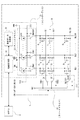
図2は、表示部10、アノードドライバ33、カソードドライバ21の構成を等価回路として示したものである。
図2に示すように表示部10においては走査線SLとデータ線DLの交点毎に画素Gが配置され、マトリクス状に配置された画素Gによって表示画像が形成される。図2では画素Gを、OLEDを表すダイオード記号と寄生容量を表す容量記号で示している。
FIG. 2 shows the configuration of the
As shown in FIG. 2, in the
カソードドライバ21には、各走査線SL1〜SL128を、それぞれ電圧VHCに接続するか、グランドに接続するかを選択するスイッチSWC1〜SWC128が設けられている。非選択状態の走査線SLは電圧VHCに接続されており、選択されている走査対象の走査線SLはグランドに接続される。つまりこの場合、選択レベルの走査信号とはグランド電位状態となる。走査線SL1〜SL128が順次グランド接続されることで、順次選択状態となる。
The
アノードドライバ33においては、各データ線DL1〜DL256に対応して定電流源I1〜I256と、スイッチSWA1〜SWA256が設けられている。
各データ線DL1〜DL256に対しては、選択状態の走査線SLの256個の画素Gに対し、各表示データ(階調値)に応じた期間長だけ、定電流源I1〜I256からの定電流(データ線駆動信号)が与えられるように、スイッチSWA1〜SWA256が駆動制御信号ADSによって制御される。
In the
For each of the data lines DL1 to DL256, for the 256 pixels G of the scanning line SL in the selected state, a constant length from the constant current sources I1 to I256 is set for a period length corresponding to each display data (tone value). Switches SWA1 to SWA256 are controlled by drive control signal ADS such that a current (data line drive signal) is applied.
アノードドライバ33が設定された電流値による定電流のデータ線駆動信号を、各画素の階調に応じた期間だけデータ線DL1〜DL256に供給するための、より具体的な構成例を図3に示す。
アノードドライバ33には、基準電流生成部33aと電流出力部33bが設けられる。
基準電流生成部33aは、電圧可変部80、差動アンプ83、PチャネルのFET(Field Effect Transistor)81、NチャネルのFET82、及び抵抗84を有する。
差動アンプ83の非反転入力には電圧可変部80からの電圧VRが印加され、反転入力は抵抗84を介して接地されている。電圧可変部80の電圧VRは電流値制御信号ISにより可変制御される。
差動アンプ83の出力端はFET82のゲートに接続され、FET82のソースは差動アンプ83の反転入力に接続され、FET82のドレインはFET81のドレインに接続されている。
A more specific configuration example for supplying a data line drive signal of a constant current according to the current value set by the
The
The reference current generation unit 33a includes a
The voltage VR from the
The output end of the
FET81はゲートがFET81のドレインに接続され、ソースが電圧VHAに接続され、ドレインがFET82のドレインに接続されている。
この構成により、FET81のソース−ドレインには、電圧VRに応じた基準電流IRが流れる。つまり基準電流IRの電流値は、電流値制御信号ISにより可変制御されることになる。
The gate of the
With this configuration, the reference current IR flows to the source-drain of the
電流出力部33bには、各データ線DL1〜DL256に対応して、データ線DLを電流源に接続する状態とグランドに接続する状態を切り替えるためのスイッチ86、87とPチャネルのFET85が設けられている。
各FET85はソースが電圧VHAに接続され、ドレインがスイッチ86に接続される。各FET85のゲートはFET81のドレイン及びゲートに接続されている。
スイッチ86がオン、スイッチ87がオフとされることで、各データ線DL1〜DL256は、各FET85のドレインと接続される。またスイッチ86がオフ、スイッチ87がオンとされることで、各データ線DL1〜DL256はグランドに接続される。
そしてこの場合、FET81と各FET85がカレントミラー構成を採る。従って、スイッチ86がオン、スイッチ87がオフのとき、データ線DLには、基準電流IRの電流値の定電流信号とされたデータ線駆動信号が与えられる。
スイッチ86、87は駆動制御部31からの駆動制御信号ADSによりオン/オフされる。例えばスイッチ86がPチャネルFET、スイッチ87がNチャネルFETとされた場合、駆動制御信号ADSがL(Low)レベルのときにデータ線DLに定電流供給が行われ、駆動制御信号ADSがH(High)レベルのときにデータ線DLが接地される。
The current output unit 33b is provided with
The source of each
Each of the data lines DL1 to DL256 is connected to the drain of each
In this case, the
The
以上の構成から理解されるように、まずデータ線DLに与えられるデータ線駆動信号としての定電流値は、電流値制御信号ISによって可変設定される。またデータ線DLにデータ線駆動信号が与えられる期間は、駆動制御信号ADSによって制御される。従って駆動制御信号ADSが階調値に応じた期間長のパルス信号とされることで、データ線DLへの定電流(データ線駆動信号)供給期間が、階調値に応じて制御され、これによって画素Gが階調に応じた輝度の発光を行うものとなる。
なお図3に示されるアノードドライバ33と図2に示されるアノードドライバ33との対応でいえば、図3のスイッチ86,87の組が図2のスイッチSWA1〜SWA256に相当し、図3の他の各部が、図2の定電流源I1〜I256に相当するといえる。
As understood from the above configuration, the constant current value as the data line drive signal applied to the data line DL is variably set by the current value control signal IS. A period in which the data line drive signal is supplied to the data line DL is controlled by the drive control signal ADS. Therefore, by setting the drive control signal ADS as a pulse signal having a period length corresponding to the gradation value, the constant current (data line drive signal) supply period to the data line DL is controlled according to the gradation value. Thus, the pixel G emits light of luminance according to the gradation.
In the correspondence between the
<2.表示上に発生する輝度変化の説明>
ここで表示上に発生する輝度変化について説明しておく。
図4は、表示上の輝度ムラの様子を模式的に示している。表示画面を領域AR1,AR2,AR3,AR4に分けて示しているが、各領域AR1,AR2,AR3,AR4は、それぞれ或る数のラインで構成される領域としている。例えば領域AR4は走査線SL1〜SL32の範囲、領域AR3は走査線SL33〜SL64の範囲、領域AR2は走査線SL65〜SL96の範囲、領域AR1は走査線SL97〜SL128の範囲などとする。
表示している階調は2種類で、非点灯と、点灯状態の或る階調値である。領域d1は非点灯画素の部分である。例えば256階調表現を行っているとすると、階調値=0/255の部分である。領域d2は、或る階調値(x/255)での点灯画素の部分である。xは1〜255のいずれかの値であり、例えばx=128などと考えれば良い。
領域AR1の各ラインは、1ライン全て階調値(x/255)で点灯している。
領域AR2の各ラインは、1ラインのうち1/4の画素が非点灯(0/255)で、3/4の画素が階調値(x/255)で点灯している。
領域AR3の各ラインは、1ラインのうち1/2の画素が非点灯(0/255)で、1/2の画素が階調値(x/255)で点灯している。
領域AR4の各ラインは、1ラインのうち3/4の画素が非点灯(0/255)で、1/4の画素が階調値(x/255)で点灯している。
このように各領域AR1,AR2,AR3,AR4における点灯画素は、全て同じ階調(x/255)で点灯しているにも関わらず、図で模式的に示すように、輝度差が生じている。即ち非点灯画素数が少ないラインほど点灯画素が明るくなり、非点灯画素数が多いラインほど点灯画素が暗くなってしまう。
このように各ラインでは点灯率に応じた輝度変動が生じる。なおここでは点灯率とは、
点灯率=(1ラインの発光画素数)/(1ラインの画素数)
としている。
<2. Explanation of the luminance change that occurs on the display>
Here, the change in luminance occurring on the display will be described.
FIG. 4 schematically shows the state of the luminance unevenness on the display. Although the display screen is shown divided into areas AR1, AR2, AR3, and AR4, each of the areas AR1, AR2, AR3, and AR4 is an area configured by a certain number of lines. For example, the area AR4 is a range of the scanning lines SL1 to SL32, the area AR3 is a range of the scanning lines SL33 to SL64, the area AR2 is a range of the scanning lines SL65 to SL96, and the area AR1 is a range of the scanning lines SL97 to SL128.
There are two types of gradation displayed, and there are certain gradation values in the non-lighting state and in the lighting state. The area d1 is a part of the non-lighting pixel. For example, assuming that 256 gradations are expressed, the gradation value is 0/255. The area d2 is a portion of the lit pixel at a certain gradation value (x / 255). x may be any value of 1 to 255, and may be considered as, for example, x = 128.
The lines in the area AR1 are all lit with gradation values (x / 255) for one line.
In each line of the area AR2, 1⁄4 of 1 line of pixels is non-lighting (0/255), and 3⁄4 of pixels is lighted with gradation value (x / 255).
In each line of the area AR3, half of the pixels in one line are not lit (0/255) and half of the pixels are lit at the gradation value (x / 255).
In each line of the area AR4, 3/4 of 1 line of pixels are non-lighted (0/255), and 1⁄4 of pixels are lighted with gradation value (x / 255).
Thus, although the lighting pixels in each of the areas AR1, AR2, AR3, and AR4 are all lit at the same gradation (x / 255), as shown schematically in the figure, a luminance difference occurs. There is. That is, the lighted pixels become brighter as the line having a smaller number of non-lighted pixels, and the lighted pixels become darker as the line has a larger number of non-lighted pixels.
As described above, in each line, luminance variation occurs according to the lighting rate. Here, the lighting rate is
Lighting rate = (number of light emitting pixels in one line) / (number of pixels in one line)
And
このような輝度ムラの原因は次のように考えられる。
図5Bは、点灯率が高いラインのモデルであり、ここでは全データ線DLに発光駆動電流が与えられている状態を示している。電圧VHCの走査線SLは非選択状態であり、0Vとされた走査線SLが選択中のラインとなる。この場合、各データ線DLに与えられた電流は、破線で示すように選択中の走査線SLに流れる。
The cause of such uneven brightness is considered as follows.
FIG. 5B is a model of a line with a high lighting rate, and here shows a state in which a light emission drive current is given to all the data lines DL. The scanning line SL of the voltage VHC is in the non-selected state, and the scanning line SL set to 0 V is the line being selected. In this case, the current applied to each data line DL flows to the scanning line SL being selected as indicated by the broken line.
図5Cは点灯率が低いラインのモデルとして、一部のデータ線DLに電流が与えられ、他のデータ線は0V(例えば接地)とされている状態を示している。
この場合、点灯画素に対応するデータ線DLに与えられる電流は、破線で示すように選択中の走査線SLだけでなく、非点灯画素に対応するデータ線DLにも流れる。このためコンデンサの記号で示す各画素の容量成分のうち、非点灯画素の寄生容量に対する充電も行われることになり負荷が重くなる結果、発光駆動電流の立ち上がりが遅れるという事象が発生する。
FIG. 5C shows a state in which a current is supplied to a part of data lines DL and the other data lines are set to 0 V (for example, ground) as a model of a line with a low lighting rate.
In this case, the current supplied to the data line DL corresponding to the lit pixel flows not only to the scanning line SL being selected but also to the data line DL corresponding to the non-lit pixel, as indicated by the broken line. Therefore, among the capacitance components of each pixel indicated by the symbol of the capacitor, the parasitic capacitance of the non-lighting pixel is also charged, and the load becomes heavy. As a result, an event occurs that the rising of the light emission drive current is delayed.
以上を踏まえて考えると、図4の領域AR1のような点灯率の高いラインの画素に対する発光駆動電流は図5Aの実線、領域AR4のような点灯率の低いラインの画素に対する発光駆動電流は図5Aの破線のようになる。
つまり点灯率が高いラインの点灯画素に対する発光駆動電流は立ち上がりが早くなり、点灯率が低いラインの点灯画素に対する発光駆動電流は立ち上がりが遅くなる。
これによって図4に示したような輝度ムラが発生していると考えられる。
Considering the above, the light emission drive current for the pixels of the line with high lighting rate such as the area AR1 in FIG. 4 is the light emission drive current for the pixels in the line with low lighting rate such as the solid line in FIG. It looks like the dashed line of 5A.
That is, the light emission drive current for the lighted pixels of the line having a high lighting rate rises quickly, and the light emission drive current for lighted pixels of the line having a low lighting rate rises late.
It is considered that this causes uneven brightness as shown in FIG.
<3.第1の実施の形態の表示駆動動作>
実施の形態では、以上のように生じる輝度ムラに対応するために、非点灯画素に対してもデータ線駆動信号としてわずかな期間だけ定電流供給を行うようにする。
以下、このための構成を説明する。
なお第1及び第2の実施の形態でいう表示データ(DT)とは、MPU2からコントローラIC20に転送される段階の各画素の階調値を表す所定ビット数のデータである。
<3. Display Drive Operation of First Embodiment>
In the embodiment, in order to cope with the uneven brightness as described above, the constant current is supplied also to the non-lighted pixel as a data line drive signal only for a short period.
The configuration for this will be described below.
The display data (DT) in the first and second embodiments is data of a predetermined number of bits representing the gradation value of each pixel at the stage of being transferred from the
図6は、表示駆動装置として機能するコントローラIC20の内部を示しているが、特に駆動制御部31内を詳細に示したものである。
駆動制御部31内には、MPUインターフェース41、コマンドデコーダ42、発振回路43、タイミングコントローラ44、電流設定部45が設けられる。
FIG. 6 shows the inside of the
In the
MPUインターフェース41は、上述したMPU2との間の各種通信を行うインターフェース回路部である。具体的には表示データやコマンド信号、輝度設定値の送受信がMPUインターフェース41とMPU2の間で行われる。
コマンドデコーダ42は、MPU2から送信されてきたコマンド信号を図示しない内部レジスタに取り込むと共に、コマンド信号のデコードを行う。そしてコマンドデコーダ42は、取り込んだコマンド信号の内容に応じた動作を実行させるべく、タイミングコントローラ44に必要な通知を行う。またコマンドデコーダ42は取り込んだ表示データを表示データ記憶部32に記憶させる。
The
The
発振回路43は、表示駆動制御のためのクロック信号CKを発生させる。
クロック信号CKは表示データ記憶部32に供給されてデータの書込/読出動作のクロックとして用いられる。またクロック信号CKはタイミングコントローラ44の処理に使用される。
The
The clock signal CK is supplied to the display
電流設定部45は、MPUインターフェース41を介してMPU2から指示された輝度設定値を取り込む。そして指示された輝度設定値に応じて電流値制御信号ISをアノードドライバ33に供給する。
図3で説明したように電流値制御信号ISによってデータ線駆動信号としての定電流値が制御される。つまりMPU2からの指示によって表示部10による画面の全体輝度を制御(ディミング制御)できる構成としている。
The
As described with reference to FIG. 3, the constant current value as the data line drive signal is controlled by the current value control signal IS. That is, the entire luminance of the screen by the
タイミングコントローラ44は、表示部10の走査線SL、データ線DLの駆動タイミングを設定する。そしてタイミングコントローラ44はカソードドライバ制御信号CAを出力して、カソードドライバ21によるライン走査を実行させる。
またタイミングコントローラ44はアノードドライバ33に駆動制御信号ADSを出力してデータ線DLの駆動(データ線駆動信号としての定電流出力)を実行させる。またこの動作のために、表示データを表示データ記憶部32から読み出し、表示データに基づいて駆動制御信号ADSを生成する。これにより、アノードドライバ33が、各走査線SLの走査タイミングにあわせて、該当ラインの各画素に駆動制御信号に応じた定電流(データ線駆動信号)の出力を行うことになる。
The
Further, the
図7にタイミングコントローラ44の具体的な構成例を示す。
タイミングコントローラ44は上述の表示データ記憶部32に記憶された表示データDTを1ライン単位でバッファ52に取り込みながら、駆動制御信号ADSの生成を行う。
バッファ52には、表示データ記憶部32から読み出された1ライン分の表示データDT(256画素の表示データ)がバッファリング(一時保存)される。表示データDTは例えば1画素につき8ビットで256階調(「0/255」〜「255/255」)を表現するデータである。
A specific configuration example of the
The
The
バッファリングされた1ライン分の表示データDT、即ち256画素分の表示データは、1画素分(8ビット)毎にセレクタ53に供給される。セレクタ53は、8ビットで表現される階調値に応じて、階調テーブル記憶部54に記憶された目標カウンタ値を選択して出力する。
階調テーブル記憶部54に記憶された階調テーブルは、例えば図8Aに示すように、8ビットバイナリデータと目標カウンタ値が対応づけられたテーブル構造とされている。なお図8Aでは参考のため、階調値とパルス幅も加えて示しているが、これらは実際のテーブルデータとして記憶する必要はない。
階調値は8ビットバイナリデータ「00000000」〜「11111111」で表される256階調を「0/255」〜「255/255」と表記したものである。
「0/255(=00000000)」は最低輝度の黒表示階調で、画素を非点灯とすることを指示する情報である。
「1/255(=00000001)」〜「255/255(=11111111)」は画素の点灯指示の情報であり、「255/255」は最高輝度の白表示階調である。
パルス幅は、目標カウンタ値によって制御されるデータ線駆動信号としてのパルス幅を時間値で示したもので、これはアノードドライバ33の定電流出力の時間長となる。
この例では、あくまで一例であるが、目標カウンタ値の1カウントを0.125μs相当としており、例えば目標カウンタ値=1020であれば、パルス幅は127.5μsとなる。
The buffered display data DT for one line, that is, the display data for 256 pixels is supplied to the
The gradation table stored in the gradation
The gradation values represent 256 gradations represented by 8-bit binary data "00000000" to "11111111" as "0/255" to "255/255".
“0/255 (= 00000000)” is information indicating that the pixel is not lit at the black display gradation of the lowest luminance.
“1/255 (= 00000001)” to “255/255 (= 11111111)” are information of a lighting instruction of the pixel, and “255/255” is a white display gradation of the highest luminance.
The pulse width represents the pulse width as a data line drive signal controlled by the target counter value as a time value, which is the time length of the constant current output of the
In this example, although this is merely an example, one count of the target counter value corresponds to 0.125 μs, and for example, if the target counter value = 1020, the pulse width is 127.5 μs.
本実施の形態の場合、「0/255」階調に対応する目標カウンタ値=1としている。
「0/255」階調、つまり表示データ「00000000」は、非点灯指示の情報である。このため通常は目標カウンタ値=0とし、「0/255」階調の画素のデータ線DLに対しては、アノードドライバ33は定電流出力を行わない。
これに対して本実施の形態では、目標カウンタ値=1としていることで、非点灯の画素に対しても、例えば0.125μsの期間、定電流供給を行うことになる。
なお、目標カウンタ値=1としているのは一例であり、目標カウンタ値=2,或いは目標カウンタ値=3とすることもあり得る。
In the case of the present embodiment, the target counter value corresponding to “0/255” gradation is set to 1.
“0/255” gradation, that is, display data “00000000” is information of non-lighting instruction. Therefore, normally, the target counter value is set to 0, and the
On the other hand, in the present embodiment, by setting the target counter value = 1, constant current supply is performed also for a non-lighted pixel, for example, for a period of 0.125 μs.
Note that the target counter value = 1 is an example, and the target counter value = 2 or the target counter value = 3 may be set.
図7の構成において、セレクタ53は、8ビットバイナリデータで表現される表示データDTに応じて、この階調テーブルを参照し、目標カウンタ値CTを読み出して出力する。例えば8ビットの表示データが「11111101」(253/255階調)である場合、目標カウンタ値=1012を出力する。
このように目標カウンタ値CTは、表示データDTとしての階調値を、実際に電流供給を行う時間を制御する値に変換したものである。
セレクタ53から出力された目標カウンタ値CTは、ラッチ回路60(60−1〜60−256)にラッチされる。
In the configuration of FIG. 7, the
As described above, the target counter value CT is obtained by converting the gradation value as the display data DT into a value for controlling the time for which the current is actually supplied.
The target counter value CT output from the
ラッチ回路60は、1ライン分の各画素に対応して複数個(本例ではラッチ回路60−1〜60−256の256個)設けられている。そして1ライン分の各画素の目標カウンタ値CTは、それぞれ対応するラッチ回路60にラッチされる。従って、1ライン分の各画素についての目標カウンタ値CTが、それぞれラッチ回路60−1〜60−256に取り込まれる。
各ラッチ回路60−1〜60−256にラッチされた目標カウンタ値CTは、それぞれ比較回路62(62−1〜62−256)において、カウンタ61のカウント値と比較され、その比較結果として、各データ線DLについての駆動制御信号ADSが得られる。
A plurality of latch circuits 60 (256 pieces of latch circuits 60-1 to 60-256 in this example) are provided corresponding to each pixel for one line. The target counter value CT of each pixel for one line is latched by the
The target counter value CT latched by each of the latch circuits 60-1 to 60-256 is compared with the count value of the
この動作を図8Bで説明する。カウンタ61は所定のクロック信号に応じて所定上限値までのカウントアップを繰り返す。所定上限値は走査線SLの1ライン期間に対応した値に設定される。比較回路62の出力は、カウンタ値のリセットタイミングでLレベルに立ち下がる。そしてカウンタ値が、ラッチされた目標カウンタ値CTに達すると、比較回路62の出力はHレベルに立ち上がる。
例えば或るラッチ回路62−xにラッチされた目標カウンタ値CT=Dpw1の場合、比較回路62−xからの比較出力として駆動制御信号ADS1が得られる。また、或るラッチ回路62−yにラッチされた目標カウンタ値CT=Dpw2の場合、比較回路62−yからの比較出力として駆動制御信号ADS2が得られる。
結局、比較回路62−1〜62−256の出力は、それぞれ対応するラッチ回路60−1〜60−256にラッチされた目標カウンタ値CTに応じた時間長のパルスとなる。
このような各比較出力が各データ線DL1〜DL256についての駆動制御信号ADSとしてアノードドライバ33に供給される。図3で説明したようにアノードドライバ33は、各駆動制御信号ADSのパルスのLレベル期間に、各データ線DL1〜DL256に定電流(データ線駆動信号)の出力を行う。
これによって表示データDTに示された階調に応じた時間長の定電流出力が、各データ線DLに対して行われる。
This operation is described in FIG. 8B. The
For example, in the case where the target counter value CT = Dpw1 latched by a certain latch circuit 62-x, the drive control signal ADS1 is obtained as a comparison output from the comparison circuit 62-x. Further, when the target counter value CT = Dpw2 latched by a certain latch circuit 62-y, the drive control signal ADS2 is obtained as a comparison output from the comparison circuit 62-y.
As a result, the outputs of the comparison circuits 62-1 to 62-256 become pulses of a time length corresponding to the target counter value CT latched by the corresponding latch circuits 60-1 to 60-256.
Such comparison outputs are supplied to the
As a result, a constant current output of a time length corresponding to the gradation indicated in the display data DT is performed on each data line DL.
以上の構成により、本実施の形態においてアノードドライバ33が各データ線DLに出力するデータ線駆動信号としては、非点灯画素に対してもわずかな時間、定電流供給を行うものとなる。
図9Aに走査線駆動信号とデータ線駆動信号の例を示す。
走査線駆動信号として、カソードドライバ21から走査線SL1,SL2,SL3に与えられる信号を示している。走査線駆動信号がLレベルとなる期間が、その走査線が選択状態となる期間である。なおブランキング信号BKは、全ての画素を発光駆動しないタイミング(ブランキング期間)を規定する信号であり、この図9Aはいわゆる「Lブランキング駆動」として、ブランキング信号BKのHレベルで示されるブランキング期間には、全ての走査線SL及びデータ線DLはLレベルとされる例である。ブランキング期間においてはデータ線駆動信号としての定電流供給は行われない。
With the above configuration, as the data line drive signal output by the
FIG. 9A shows an example of a scanning line drive signal and a data line drive signal.
As scanning line drive signals, signals given from the
走査線駆動信号により、各走査線SL1,SL2・・・が、順次選択状態とされる。走査線駆動信号としてLレベルが与えられることで各走査線SLが選択される。
ここでデータ線DLpは、走査線SL1,SL2,SL3上の各画素が、それぞれ表示データDTで指定される階調で発光される画素に定電流を供給するデータ線であるとする。
このデータ線DLpには、データ線駆動信号として、選択された走査線SL上の各画素の階調に応じた時間長(TK1,TK2,TK3)で定電流が供給される。図のパルス波形がアノードドライバ33の出力端子電圧であり、これは定電流供給期間を示すことになる。このHレベルのパルス期間、即ちアノードドライバ33のデータ線DLpに対する出力端子電圧=VHA(図2,図3参照)とされる期間が、各画素の発光期間となり、その長短で階調が表現される。
The scan lines SL1, SL2,... Are sequentially selected by the scan line drive signal. Each scanning line SL is selected by giving L level as a scanning line drive signal.
Here, it is assumed that the data line DLp is a data line for supplying a constant current to the pixels in which each pixel on the scanning lines SL1, SL2 and SL3 emits light at the gradation designated by the display data DT.
A constant current is supplied to the data line DLp as a data line drive signal with a time length (TK1, TK2, TK3) corresponding to the gradation of each pixel on the selected scanning line SL. The pulse waveform in the figure is the output terminal voltage of the
一方、データ線DLqは、走査線SL1,SL2,SL3上の各画素が、それぞれ表示データDTで階調「0/255」が指定された、非点灯画素となっているデータ線であるとする。
このデータ線DLqには、通常は、全く定電流供給が行われないところ、本実施の形態では図示のように、或る所定の期間(非点灯用時間長TK0)だけ、定電流供給が行われる。即ちアノードドライバ33のデータ線DLqに対しても出力端子電圧=VHAとされる。この非点灯用時間長TK0の定電流供給は、発光される画素に対するデータ線DLpの定電流供給の開始タイミングから行われる。
これは、図8Aのように表示データ「00000000(=0/255階調)」に対して、目標カウンタ値CT=1と設定されていることによる。表示データDTで規定される階調値が非点灯を示す値であるにもかかわらず、目標カウンタ値CT=1とされることで、例えば非点灯用時間長TK0=0.125μsの期間、非点灯画素にも定電流が与えられる。
On the other hand, data line DLq is a data line in which each pixel on scanning lines SL1, SL2 and SL3 is a non-lighting pixel for which gradation "0/255" is designated by display data DT. .
Normally, constant current supply is not performed at all to data line DLq. In the present embodiment, as shown in the figure, constant current supply is performed for a predetermined period (non-lighting time length TK0). It will be. That is, the output terminal voltage = VHA is also applied to the data line DLq of the
This is because the target counter value CT = 1 is set for the display data “00000000 (= 0/255 gradation)” as shown in FIG. 8A. Even though the gradation value defined by the display data DT is a value indicating non-lighting, by setting the target counter value CT = 1, for example, a non-lighting time length TK0 = 0.125 μs A constant current is also applied to the lit pixels.
このように非点灯画素に対しても非点灯用時間長TK0だけ定電流を与えることで、図4で説明した輝度ムラの発生を抑制できる。
これは、点灯開始時点で図5Bの状態となり、非点灯用時間長TK0を経過すると図5Cの状態になるという動作として、図5Bの状態が瞬間的に発生することによる。即ち非点灯画素の寄生容量への充電が発生し、図5Cの状態になった時点で非点灯画素の寄生容量への充電のための負荷が軽減される。このため点灯率の低いラインにおける発光駆動電流の立ち上がりが改善される。
従って発光駆動電流は、ラインの点灯率に関わらず、ほぼ図5Aの実線のようになり、これによって図4のような輝度ムラの発生が抑制される。
As described above, by applying the constant current for the non-lighting time length TK0 also to the non-lighting pixel, the occurrence of the uneven brightness described with reference to FIG. 4 can be suppressed.
This is because the state of FIG. 5B is generated instantaneously as an operation of becoming the state of FIG. 5B at the lighting start time point and becoming the state of FIG. 5C after the non-lighting time length TK0. That is, charging to the parasitic capacitance of the non-lighting pixel occurs, and the load for charging to the parasitic capacitance of the non-lighting pixel is reduced when the state of FIG. 5C is reached. Therefore, the rise of the light emission drive current in the line with a low lighting rate is improved.
Accordingly, regardless of the lighting rate of the line, the light emission drive current is substantially as shown by the solid line in FIG. 5A, whereby the occurrence of the uneven brightness as shown in FIG. 4 is suppressed.
ところで非点灯画素は、本来は電流を流さないことで輝度ゼロ、つまり全く点灯させない状態としていたものである。このため、電流を流すことで発光状態となってしまえば、0/255階調がなくなり、階調表現が阻害され表示品質が低下する。
そこで本実施の形態は、非点灯画素への電流供給を行う非点灯用時間長TK0は非常に短い時間としている。つまり視覚上、点灯と認識できない程度の時間とする。
非点灯用時間長をどのような時間長にするかは多様に考えられるが、まず、少なくとも1つ上の階調、少なくとも1/255階調の定電流供給時間(図8Aの例でいえば0.5μs)よりは短くする。このようにしないと、0/255階調が消失することになるためである。
また少なくとも1/255階調の定電流供給時間の1/2以下の時間長とすることが望ましい。そのような時間長であれば、階調を明確にわけることができ、また非点灯と認識されるレベルとなるからである。
By the way, the non-lighting pixel is a state in which the luminance is zero, that is, the state where it is not lighted at all by originally not flowing a current. For this reason, if the light emission state is achieved by supplying a current, the 0/255 gradation disappears, the gradation expression is disturbed, and the display quality is degraded.
Therefore, in the present embodiment, the non-lighting time length TK0 for supplying the current to the non-lighting pixel is a very short time. In other words, it is time that can not be recognized visually as lighting.
There are various possibilities for how long the non-lighting time is to be used. First, a constant current supply time of at least one gradation higher than at least 1/255 gradation (in the example of FIG. 8A Make it shorter than 0.5 μs). If this is not done, 0/255 gradation will be lost.
Further, it is desirable that the time length be at least 1/2 of the constant current supply time of at least 1/255 gradation. With such a time length, it is possible to clearly distinguish the gradation and to obtain a level at which it is recognized as non-lighting.
なお電流値や画素の発光効率などにもよるため一概には言えないが、実際上、1μs以下の発光では、人は発光を認識することが困難になる。そのため非点灯用時間長TK0は少なくとも1μs以下の範囲であることが望ましい。例えば階調数の設定が16階調(0/15階調〜15/15階調)などと少なくなる場合、1/15階調の定電流供給期間が6〜7μsなどなることも考えられるが、そのような場合に、非点灯用時間長TK0は1μs以下であることが望ましいということになる。 Note that although it depends on the current value and the light emission efficiency of the pixel, it can not be generally said, but in fact, with light emission of 1 μs or less, it becomes difficult for a person to recognize light emission. Therefore, it is desirable that the non-lighting time length TK0 be in the range of at least 1 μs or less. For example, when the setting of the number of gradations is reduced to 16 gradations (0/15 gradations to 15/15 gradations), the constant current supply period of 1/15 gradations may be 6 to 7 μs. In such a case, it is desirable that the non-lighting time length TK0 be 1 μs or less.
<4.第2の実施の形態>
第2の実施の形態について説明する。第2の実施の形態は、図9AのようなLブランキング駆動ではなく、図9Bのようにブランキング期間に、走査線SL及びデータ線DLを特定電位状態(この例では電圧VHC)とする駆動方式を用いる例である。
図示のように、ブランキング信号BKのHレベルで規定されるブランキング期間において、全ての走査線SL及びデータ線DLは電圧VHCにセットされ、データ線駆動信号としての定電流供給は行われない。
ブランキング期間の終了後、データ線DLpにはアノードドライバ33の出力端子電圧VHA(VHC<VHA)とされる定電流供給が、選択された走査線SL上の各画素の階調に応じた時間長だけ行われる。
同時にこの場合も、データ線DLqに、アノードドライバ33の出力端子電圧VHAとされる定電流供給が、非点灯用時間長TK0だけ行われる。
<4. Second embodiment>
The second embodiment will be described. In the second embodiment, the scanning line SL and the data line DL are set to a specific potential state (voltage VHC in this example) in the blanking period as shown in FIG. 9B, not L blanking driving as shown in FIG. 9A. It is an example using a drive system.
As shown, in the blanking period defined by the H level of blanking signal BK, all scan lines SL and data lines DL are set to voltage VHC, and constant current supply as a data line drive signal is not performed. .
After the end of the blanking period, a constant current supplied to the data line DLp as the output terminal voltage VHA (VHC <VHA) of the
At the same time, also in this case, a constant current supplied to the data line DLq as the output terminal voltage VHA of the
このための構成例を図10に示す。図10は図2と同様に表示部10、アノードドライバ33、カソードドライバ21の構成を等価回路として示したものである。図2と同一部分は同一符号を付し、説明を省略する。
この場合、アノードドライバ33では、スイッチSWA1〜SWA256が、3系統を選択的にデータ線DL1〜DL256に接続する構成とされる。即ち各データ線DL(DL1〜DL256)は、スイッチSWA1〜SWA256により、定電流源(I1〜I256)が接続された状態と、グランドが接続された状態と、電圧VHCが接続された状態に切り替えられる。
そして駆動制御部31からアノードドライバ33にはブランキング信号BKも供給され、スイッチSWA1〜SWA256はブランキング期間において、各データ線DL1〜DL256を電圧VHCに接続した状態とする。
カソードドライバ21では、スイッチSWC1〜SWC128がブランキング期間において電圧VHC側を選択していることで、走査線駆動信号はHレベル(=VHC)とされる。
A configuration example for this is shown in FIG. Similar to FIG. 2, FIG. 10 shows the configuration of the
In this case, in the
The blanking signal BK is also supplied from the
In the
この第2の実施の形態において他の構成は第1の実施の形態と同様である。
図9Aの場合と同様に、図9Bのデータ線DLpが、点灯画素が接続されているデータ線であるとすると、このデータ線DLpには、データ線駆動信号として、選択された走査線SL上の各画素の階調に応じた時間長(TK1,TK2,TK3)で定電流が供給される。
また、データ線DLqが、走査線SL1,SL2,SL3上の各画素が、それぞれ表示データDTで階調「0/255」が指定された、非点灯画素となっているデータ線であるとする。この場合に図8Aのように表示データ「00000000(=0/255階調)」に対して、目標カウンタ値CT=1と設定されていることで、例えば非点灯用時間長TK0=0.125μsの期間、非点灯画素にも定電流が与えられる。
これにより第1の実施の形態と同様、輝度ムラの発生が抑制される。
Other configurations in the second embodiment are the same as those in the first embodiment.
Similarly to the case of FIG. 9A, assuming that data line DLp of FIG. 9B is a data line to which lighting pixels are connected, data line DLp is selected on data scan line SL as a data line drive signal. A constant current is supplied for a time length (TK1, TK2, TK3) corresponding to the gradation of each pixel.
Further, it is assumed that data line DLq is a data line which is a non-lighting pixel in which each pixel on scanning lines SL1, SL2 and SL3 is a gray scale "0/255" designated by display data DT. . In this case, as shown in FIG. 8A, for the display data “00000000 (= 0/255 gradation)”, the target counter value CT = 1 is set, for example, the non-lighting time length TK0 = 0.125 μs During the period, the constant current is also applied to the non-lighting pixels.
As a result, as in the first embodiment, the occurrence of uneven brightness is suppressed.
<5.第3の実施の形態>
第3の実施の形態は、図7の階調テーブル記憶部54に記憶する階調テーブルをMPU2からのコマンドで書き換えるようにした例である。
具体的にはMPU2は階調テーブル設定コマンドを発行し、階調テーブルをコントローラIC20に受け渡して更新させる。
<5. Third embodiment>
The third embodiment is an example in which the gradation table stored in the gradation
Specifically, the
図11に、MPU2からの階調テーブル設定コマンドに対するコントローラIC20(駆動制御部31)の処理を示す。
ステップS101として駆動制御部31は階調テーブル設定コマンドを監視する。階調テーブル設定コマンドが受信された場合はステップS102に進み、駆動制御部31はMPU2から送信されてくる階調テーブルを取り込む。
そして駆動制御部31はステップS103でアノードドライバ33における階調テーブル記憶部54の書き換えを行う。
これにより各階調値に対応するパルス幅が異なる階調テーブルに更新される。
FIG. 11 shows the processing of the controller IC 20 (drive control unit 31) in response to the tone table setting command from the
In step S101, the
Then, in step S103, the
As a result, the pulse width corresponding to each gradation value is updated to a different gradation table.
具体的には、0/255階調「00000000」に対応する目標カウンタ値CTが異なる階調テーブルに更新される。
つまりMPUは、1/255階調〜255/255階調についての目標カウンタ値CTが共通の階調テーブルであって、0/255階調に対応する目標カウンタ値CTのみが異なる複数の階調テーブルを用意しておき、これらの内で選択した階調テーブルをコントローラIC20に与えるようにする。
Specifically, the target counter value CT corresponding to the 0/255 gradation "00000000" is updated to a different gradation table.
That is, the MPU is a gradation table in which the target counter values CT for 1/255 gradation to 255/255 gradations are common, and a plurality of gradations different only in the target counter value CT corresponding to 0/255 gradations A table is prepared, and the gradation table selected from these is provided to the
これによって非点灯画素に対する定電流供給時間を微調整できる。
例えばパネルサイズや1ラインの画素数などにより、適切な非点灯用時間長が異なることが考えられる。そこで接続するパネルに応じて階調テーブルを変更することでフレキシブルに対応できることになる。
なお、0/255階調だけでなく、1/255〜255/255階調の目標カウンタ値CTの異なる階調テーブルを用意して、更新できるようにしても良いことは言うまでもない。
This allows fine adjustment of the constant current supply time for the non-lighting pixels.
For example, it is conceivable that the appropriate non-lighting time length differs depending on the panel size, the number of pixels in one line, and the like. Therefore, it is possible to respond flexibly by changing the gradation table according to the panel to be connected.
Needless to say, it is also possible to prepare a gradation table having different target counter values CT of not only 0/255 gradation but also 1/255 to 255/255 gradation so as to enable updating.
<6.第4の実施の形態>
第4の実施の形態を説明する。第1〜第3の実施の形態では、非点灯画素の全てに対して、非点灯用時間長の定電流供給を行うものとしたが、このような定電流供給は、全ての非点灯画素ではなく、非点灯画素の一部に対して行うものでもよい。
<6. Fourth embodiment>
A fourth embodiment will be described. In the first to third embodiments, the constant current supply for the non-lighting time length is performed for all the non-lighting pixels, but such constant current supply is performed for all the non-lighting pixels. Alternatively, it may be performed on part of non-lighted pixels.
第1〜第3の実施の形態のように非点灯画素のデータ線DLの全てに対して、非点灯用時間長の定電流供給を行うことは輝度ムラ低減の観点で有効ではあるが、機種によっては、ノイズを多く発生させてしまう場合もある。そこで、例えば非点灯画素の一部に対応してデータ線DLに非点灯用時間長の定電流供給を行うようにすることが考えられる。
例えば非点灯画素の半分(ほぼ半分)に対して非点灯用時間長の定電流供給を行う。このようにすると輝度ムラの低減を実現しつつ、ノイズ発生を抑えることができる。また電流供給を行う画素数が減ることで、消費電力を減らせることにもなる。
As in the first to third embodiments, performing constant current supply for the non-lighting time length to all the data lines DL of non-lighting pixels is effective from the viewpoint of reducing unevenness in brightness, but the model Depending on the situation, a lot of noise may be generated. Therefore, for example, it may be considered to supply a constant current for the non-lighting time length to the data line DL in correspondence with a part of the non-lighting pixels.
For example, the constant current supply for the non-lighting time length is performed for half (approximately half) of the non-lighting pixel. In this way, it is possible to suppress the occurrence of noise while realizing the reduction of the uneven brightness. In addition, power consumption can be reduced by reducing the number of pixels to which current is supplied.
特には、定電流印加を行う非点灯画素のデータ線DLは、一画面上で、一定間隔で略均等となるようにするのがよい。
ここでいう均等とは、具体的には、1ラインの中で1画素おきに、定電流印加を行うようにし、また或るラインと隣接するラインでも、定電流供給を行う画素と行わない画素の関係で隣り合うようにするとよい。即ち画面上で市松模様のように、定電流供給を行う非点灯画素と、定電流供給を行わない非点灯画素が配置されるような状態である。
In particular, it is preferable that the data lines DL of non-lighting pixels to which constant current application is performed be substantially equal at a constant interval on one screen.
Specifically, the term “equal” means that constant current application is performed every other pixel in one line, and pixels that do not supply constant current and pixels that do not supply constant current even in a line adjacent to a certain line. It is good to be adjacent to each other in relation to That is, as shown in a checkered pattern on the screen, non-lighting pixels that supply constant current and non-lighting pixels that do not supply constant current are arranged.
これを実現するには、元の表示データDTに階調値(0/255)と階調値(1/255)が水平垂直に交互に配置された背景画像データを合成することが考えられる。
図12Aに表示データDTの例を模式的に示す。
図12Aは、ある階調値による「表示画像」という画像を有する表示データに対して、階調値(1/255)と階調値(0/255)が市松模様のように交互に配置された背景データを合成したイメージを示している。
この場合、例えばコントローラIC20の表示データ記憶部32に記憶される表示データDTにおいて本来非点灯画素となる背景部分は、階調値(1/255)の画素と階調値(0/255)の画素が上下左右に交互に配置される状態となる。
In order to realize this, it is conceivable to combine background image data in which gradation values (0/255) and gradation values (1/255) are alternately arranged in the horizontal and vertical directions with the original display data DT.
FIG. 12A schematically shows an example of the display data DT.
In FIG. 12A, the gradation value (1/255) and the gradation value (0/255) are alternately arranged like a checkered pattern with respect to display data having an image "display image" by a certain gradation value. Shows an image obtained by synthesizing the background data.
In this case, for example, in the display data DT stored in the display
タイミングコントローラ44における階調テーブル記憶部54には図13の階調テーブルを記憶させる。
この階調テーブルは、階調値(0/255)に対しては、目標カウンタ値CT=0とし、つまり電流供給を行わない設定とする。また階調値(1/255)に対しては、目標カウンタ値CT=1とし、つまり0.125μsの期間だけ電流供給を行う設定とする。
このようにすれば、図12Aの右端に示した合成した表示データに応じては、非点灯画素のうちのほぼ半分については非点灯用時間長(この場合0.125μs)の定電流供給が行われ、非点灯画素のうちの残りのほぼ半分は、定電流供給が行われない画素となる。
The tone
In this gradation table, for the gradation value (0/255), the target counter value CT = 0 is set, that is, the setting is made so as not to supply the current. Further, with respect to the gradation value (1/255), the target counter value CT = 1 is set, that is, setting is made to supply current for a period of 0.125 μs.
In this way, constant current supply for the non-lighting time length (0.125 μs in this case) is performed for approximately half of the non-lighted pixels according to the combined display data shown at the right end of FIG. 12A. Approximately half of the remaining non-lighted pixels become pixels for which constant current supply is not performed.
従ってMPU2が表示データDTをコントローラIC20に供給する際に、予め図12Aのような背景データの合成を行えばよい。
即ちMPU2は、表示データDTで規定される階調値が非点灯を示す値である画素の一部に対して、アノードドライバ33によって非点灯用時間長の定電流供給が行われるように、表示データDTの階調値を変換してから、コントローラIC20(駆動制御部31)に供給する。これにより非点灯画素のうちのほぼ半分に定電流供給が行われるようにすることができ、短時間の定電流供給によるノイズ発生を抑制できる。
Therefore, when the
That is, the
但し、MPU2ではデータ変換を行わずに、コントローラIC20の駆動制御部31内において、背景データ合成部を設け、受信した表示データDTに図12Aのような背景データの合成を行い、合成した表示データDTを表示データ記憶部32に記憶させるようにしてもよい。
これによりアノードドライバ33は、元々の表示データDTで規定される階調値が非点灯を示す値である画素の一部に対して、非点灯用時間長の定電流供給を行うようにデータ線DLを駆動することになる。
或いはタイミングコントローラ44が、表示データ記憶部32から表示データDTを読み出した段階で、図12Aのような背景データの合成を行い、合成した表示データDTが8ビットずつセレクタ53に供給されるようにしてもよい。この場合もアノードドライバ33は、元々の表示データDTで規定される階調値が非点灯を示す値である画素の一部に対して、非点灯用時間長の定電流供給を行うようにデータ線DLを駆動することになる。
However, the
As a result, the
Alternatively, when the
なお、ここでは非点灯画素のほぼ半分には定電流供給を行うとしたが、非点灯画素のうちで定電流供給を行う画素の割合は、必ずしもほぼ半分が適切とは限らない。表示パネルサイズや1ラインの画素数などの設計事項に応じて、輝度ムラの低減とノイズレベルの低減が最適化できる「割合」(定電流供給を行う非点灯画素の割合)が異なるためである。従ってどの程度の割合にするかは、実際の表示装置毎に検討することが望ましい。 Here, although it is described that constant current supply is performed to approximately half of the non-lighting pixels, the proportion of pixels performing constant current supply among the non-lighting pixels is not necessarily approximately half of the ratio. This is because the “proportion” (proportion of non-lighting pixels that perform constant current supply) at which reduction of uneven brightness and reduction of noise level can be optimized differs according to design items such as the display panel size and the number of pixels in one line. . Therefore, it is desirable to consider how much the ratio should be set for each actual display device.
ところで図12Bは、ある階調の「表示画像」という画像を有する表示データに対して、階調値(1/255)の背景データを合成したイメージを示している。この場合、例えばコントローラIC20の表示データ記憶部32に記憶される表示データは、階調値(1/255)の背景にある階調の「表示画像」という画像を有する表示データとなる。
MPU2がこのように変換した表示データDTをコントローラIC20に供給すると、図13の階調テーブルを用いている場合、非点灯画素の全部に対して非点灯用時間長の定電流供給が行われることになる。つまりMPU2側の表示データ変換によって、第1の実施の形態と同様の動作を行うこともできる。
FIG. 12B shows an image obtained by combining background data of gradation value (1/255) with display data having an image of “display image” of a certain gradation. In this case, for example, the display data stored in the display
When the
<7.まとめ及び変形例>
以上の実施の形態では次のような効果が得られる。
実施の形態の表示駆動装置(コントローラIC20)は、列方向に並ぶ複数の画素に共通に接続されたデータ線DLと、行方向に並ぶ複数の画素に共通に接続された走査線SLとが、それぞれ複数配設され、データ線DLと走査線SLの各交差点に対応して画素が形成されている表示部10に対して、表示データに基づく表示駆動を行う。そして表示駆動装置(コントローラIC20)は、走査線SLの選択タイミング毎に、データ線DLのそれぞれに対して、表示データDTで規定される画素の階調値に応じた時間長だけ定電流を供給するデータ線駆動部(タイミングコントローラ44及びアノードドライバ33)を備える。このデータ線駆動部は、表示データDTで規定される階調値が非点灯を示す値(0/255)である画素の全部又は一部に対して、非点灯用時間長の定電流供給を行うようにデータ線DLを駆動するようにしている。
具体的には、表示データDT=0/255階調の場合も、0ではない目標カウント値CT(例えば1)に変換し、電流供給が行われるようにしている。
通常は非点灯の画素(その画素が接続されたデータ線DL)に対しては定電流供給を行わないことで、その画素を非点灯の状態とする。これに対して実施の形態では、非点灯の画素のデータ線DTに対しても、或る時間長(非点灯用時間長)の定電流供給を行う。
これにより非点灯画素の寄生容量への充電に起因するデータ線駆動信号の立ち上がりが、1ラインにおける非点灯画素数(点灯率)によって大きく変動しないようにできる。従って点灯率に関わらず輝度の立ち上がりを略均一化でき、輝度ムラを低減又は解消できる。
なお、第4の実施の形態で述べたように、非点灯画素の一部に対して非点灯用時間長の定電流供給を行うようにすることで、輝度ムラを低減又は解消しつつ、ノイズを抑制できる場合もある。
<7. Summary and Modifications>
The following effects can be obtained in the above embodiment.
In the display drive device (controller IC 20) according to the embodiment, a data line DL commonly connected to a plurality of pixels lined in the column direction and a scan line SL commonly connected to a plurality of pixels lined in the row direction are A display drive based on display data is performed on the
Specifically, also in the case of the display data DT = 0/255 gradation, conversion into a target count value CT (for example, 1) that is not 0 is performed, and current supply is performed.
Normally, the constant current is not supplied to the non-lighted pixel (the data line DL to which the pixel is connected), thereby making the pixel non-lighted. On the other hand, in the embodiment, constant current supply of a certain time length (non-lighting time length) is also performed to the non-lighted pixel data line DT.
As a result, the rise of the data line drive signal caused by the charging of the parasitic capacitance of the non-lighting pixel can be prevented from largely fluctuating by the number of non-lighting pixels (lighting rate) in one line. Therefore, regardless of the lighting rate, the rising of the luminance can be made substantially uniform, and the luminance unevenness can be reduced or eliminated.
Note that, as described in the fourth embodiment, by performing constant current supply for the non-lighting time length to a part of the non-lighting pixels, noise is reduced while eliminating or reducing luminance unevenness. In some cases.
また非点灯用時間長は、固定設定した或る特定の時間長としている。例えば目標カウンタ値CT=1の場合の0.125μsである。
つまり表示部10内の画素の位置、走査線、データ線等の別に関わらず、表示データにおいて階調値が非点灯階調となっている画素に対しては、非点灯用時間長としての共通の時間長の期間、定電流供給を行う。
これにより単に非点灯階調の場合に特定の非点灯用時間長の定電流供給を行えばよく、回路構成や制御が容易化される。具体的には階調テーブルの設定(0/255階調の目標カウンタ値CTの設定)で本実施の形態の動作が実現できる。従って回路変更等が不要で実施コストを低くでき、実用性は高い。
Further, the non-lighting time length is a specific time length fixed. For example, 0.125 μs in the case of the target counter value CT = 1.
That is, regardless of the position of the pixel in the
As a result, constant current supply of a specific non-lighting time length may be performed merely in the case of non-lighting gradation, and the circuit configuration and control are facilitated. Specifically, the operation of the present embodiment can be realized by setting of the gradation table (setting of the target counter value CT of 0/255 gradation). Therefore, no circuit change is required, the implementation cost can be reduced, and the practicability is high.
また非点灯用時間長は、表示データにおける点灯指示値のうちで最も低い階調(1/255)の画素に対する定電流供給時間長(例えば図8Aの場合の0.5μs)よりも短い時間長とされる。
非点灯画素に対しての定電流供給により、実際にはその画素が点灯してしまう。そこで非点灯用時間長は、点灯する画素に対する定電流供給時間長よりも短くすることで、ほとんど点灯とは認識されないような電流供給を行い、点灯画素に対する駆動と区別する。これにより点灯画素との間の階調を損なわないようにし、表示品質を良好に保つ。
The non-lighting time length is shorter than the constant current supply time length (for example, 0.5 μs in the case of FIG. 8A) to the pixel of the lowest gradation (1/255) among the lighting instruction values in the display data. It is assumed.
The constant current supply to the non-lighted pixel actually causes the pixel to light. Therefore, by setting the non-lighting time length to be shorter than the constant current supply time length for the lighted pixel, current supply is performed such that it is hardly recognized as lighted, and this is distinguished from the drive for the lighted pixel. As a result, the gradation between the lighted pixels is not lost, and the display quality is kept good.
また非点灯用時間長は、表示データにおける点灯指示値のうちで最も低い階調(1/255)の画素に対する定電流供給時間長の半分以下の時間長とする。例えば図8Aの例では0.5μsに対する半分以下の0.125μsとしている。
非灯画素に対しての定電流供給時間は、視覚上、非点灯と認識される範囲であることが表示品質の上で重要である。点灯状態の内で最も低い階調の場合の定電流供給時間長の半分以下として、視覚上は非点灯と認識されるようにする。これにより点灯画素との間の階調を損なわないようにし、表示品質を良好に保つ。
Further, the non-lighting time length is set to a time length equal to or less than half the constant current supply time length for the pixel of the lowest gradation (1/255) among the lighting instruction values in the display data. For example, in the example of FIG. 8A, it is 0.125 μs which is half or less of 0.5 μs.
It is important in terms of display quality that the constant current supply time for non-lighting pixels is a range visually recognized as non-lighting. It is visually recognized as non-lighting as half or less of the constant current supply time length in the case of the lowest gradation in the lighting state. As a result, the gradation between the lighted pixels is not lost, and the display quality is kept good.
また第3の実施の形態で説明したように、非点灯用時間長(つまり階調テーブルにおける0/255階調の目標カウンタ値CT)が外部コマンドに応じて変更可能とされている。非点灯用時間長を外部コマンドで更新できるようにすることで、非点灯用時間長を例えば表示部に応じて調整できる。これにより最適な非点灯用時間長に調整することができる。またこれはコントローラIC20としての部品の汎用化にも好適である。
As described in the third embodiment, the non-lighting time length (that is, the target counter value CT of 0/255 gradation in the gradation table) can be changed according to the external command. By allowing the non-lighting time length to be updated by an external command, the non-lighting time length can be adjusted according to, for example, the display unit. Thereby, it is possible to adjust to the optimal non-lighting time length. This is also suitable for generalization of parts as the
また第4の実施の形態において言及したが、MPU2(表示動作制御部)側で表示データを変換しておく手法によっても、全部又は一部の非点灯の画素に非点灯用時間長の定電流供給を行うようにすることができる。コントローラIC20において階調テーブルが更新できない場合、或いは階調テーブルの更新をしないようにしたい事情がある場合などは、MPU2側での表示データDTの処理により、輝度ムラの低減を実現できる。
Further, although mentioned in the fourth embodiment, the constant current of the non-lighting time length for all or part of the non-lighted pixels is also obtained by the method of converting the display data on the MPU 2 (display operation control unit) side. It can be made to supply. When the gradation table can not be updated in the
以上、実施の形態について説明したが、本発明の表示装置や表示駆動装置は実施の形態に限定されず多様な変形例が考えられる。
例えば表示駆動装置の例として図1に示したコントローラIC20は、アノードドライバ33を内蔵するものとしたが、アノードドライバ33は別体であってもよい。
またコントローラIC20に、アノードドライバ33とカソードドライバ21の両方が内蔵されていてもよい。
As mentioned above, although embodiment was described, the display apparatus and display drive apparatus of this invention are not limited to embodiment, A various modified example can be considered.
For example, although the
Further, both the
また、コントローラIC20を特定の表示パネルに専用の部品とする場合など、階調テーブルは書換不能なROMデータとして記憶しても良い。
また階調テーブルを用いずに、表示データが非点灯を示す情報のときに、対応するデータ線DLに所定の非点灯用時間長だけ電流を流す構成も各種考えられる。
また本発明はOLEDを用いる表示装置だけでなく、他の種の表示装置でも適用可能である。特に電流駆動による自発光素子を用いた表示装置に好適である。
Further, when the
In addition, various configurations are also conceivable in which current is supplied to the corresponding data line DL for a predetermined non-lighting time length when the display data is information indicating non-lighting without using the gradation table.
The present invention is applicable not only to display devices using OLEDs, but also to other types of display devices. In particular, the present invention is suitable for a display device using a self light emitting element driven by current.
1…表示装置
2…MPU
10…表示部
20…コントローラIC
31…駆動制御部
32…表示データ記憶部
33…アノードドライバ
21…カソードドライバ
44…タイミングコントローラ
45…電流設定部
53…セレクタ
54…階調テーブル記憶部
1 ...
10: Display unit 20: Controller IC
31 ...
Claims (5)
前記データ線に対して定電流供給が行われない第1の階調値とされた画素と、前記データ線に対して非点灯用時間長の定電流供給が行われる第2の階調値とされた画素とが、一画面上で略均等に配置された背景データを、表示データに合成する背景データ合成部と、
前記走査線の選択タイミング毎に、前記データ線のそれぞれに対して、前記背景データが合成された後の表示データで規定される画素の階調値に応じた時間長だけ定電流を供給するデータ線駆動部と、を備えた
表示駆動装置。 A plurality of data lines connected in common to a plurality of pixels lined in the column direction and a plurality of scanning lines connected in common to the plurality of pixels lined in the row direction are provided, each of the data lines and the scanning lines A display driving device that performs display driving based on display data with respect to a display unit in which pixels are formed corresponding to intersections.
It said second gradation value and a pixel constant current supply is a performed such have first gradation value to the data line, the non-lighting time length of the constant current supplied to the data line is performed Background data combining unit that combines background data, in which the selected pixels are substantially evenly arranged on one screen, with display data;
Data for supplying a constant current to each of the data lines for each of the data lines for a time length corresponding to the gradation value of the pixel defined by the display data after the background data is synthesized And a line driving unit.
請求項1に記載の表示駆動装置。 The background data is data in which a pixel having the first gradation value and a pixel having the second gradation value are alternately arranged in upper, lower, left, and right directions. Display driving device.
請求項1又は請求項2に記載の表示駆動装置。 The second gradation value is a gradation value in which the time length for supplying a constant current is the shortest among the gradation values for which a constant current is supplied to the data line. Display drive device as described.
前記データ線に対して定電流供給が行われない第1の階調値とされた画素と、前記データ線に対して非点灯用時間長の定電流供給が行われる第2の階調値とされた画素とが、一画面上で略均等に配置された背景データを、表示データに合成する背景データ合成部と、
前記走査線の選択タイミング毎に、前記データ線のそれぞれに対して、前記背景データが合成された後の表示データで規定される画素の階調値に応じた時間長だけ定電流を供給するデータ線駆動部と、を備えた
表示装置。 A plurality of data lines connected in common to a plurality of pixels lined in the column direction and a plurality of scanning lines connected in common to the plurality of pixels lined in the row direction are provided, each of the data lines and the scanning lines A display unit in which pixels are formed corresponding to the intersections;
A pixel having a first gradation value in which constant current supply is not performed to the data line, and a second gradation value in which constant current supply for a non-lighting time length is performed to the data line Background data combining unit that combines background data, in which the selected pixels are substantially evenly arranged on one screen, with display data;
Data for supplying a constant current to each of the data lines for each of the data lines for a time length corresponding to the gradation value of the pixel defined by the display data after the background data is synthesized And a line drive unit.
前記データ線に対して定電流供給が行われない第1の階調値とされた画素と、前記データ線に対して非点灯用時間長の定電流供給が行われる第2の階調値とされた画素とが、一画面上で略均等に配置された背景データを、表示データに合成し、
前記走査線の選択タイミング毎に、前記データ線のそれぞれに対して、前記背景データが合成された後の表示データで規定される画素の階調値に応じた時間長だけ定電流を供給する
表示駆動方法。 A plurality of data lines connected in common to a plurality of pixels lined in the column direction and a plurality of scanning lines connected in common to the plurality of pixels lined in the row direction are provided, each of the data lines and the scanning lines As a display driving method for performing display driving based on display data for a display unit in which pixels are formed corresponding to intersections,
A pixel having a first gradation value in which constant current supply is not performed to the data line, and a second gradation value in which constant current supply for a non-lighting time length is performed to the data line Background data, in which the selected pixels are approximately evenly arranged on one screen, is combined with the display data,
At each selection timing of the scanning line, a constant current is supplied to each of the data lines for a time length corresponding to a gradation value of a pixel defined by display data after the background data is synthesized. How to drive.
Priority Applications (1)
| Application Number | Priority Date | Filing Date | Title |
|---|---|---|---|
| JP2018110102A JP6514811B2 (en) | 2018-06-08 | 2018-06-08 | Display drive device, display device, display drive method |
Applications Claiming Priority (1)
| Application Number | Priority Date | Filing Date | Title |
|---|---|---|---|
| JP2018110102A JP6514811B2 (en) | 2018-06-08 | 2018-06-08 | Display drive device, display device, display drive method |
Related Parent Applications (1)
| Application Number | Title | Priority Date | Filing Date |
|---|---|---|---|
| JP2015183284A Division JP2017058522A (en) | 2015-09-16 | 2015-09-16 | Display drive device, display device and display drive method |
Publications (3)
| Publication Number | Publication Date |
|---|---|
| JP2018151666A JP2018151666A (en) | 2018-09-27 |
| JP2018151666A5 JP2018151666A5 (en) | 2018-11-08 |
| JP6514811B2 true JP6514811B2 (en) | 2019-05-15 |
Family
ID=63681684
Family Applications (1)
| Application Number | Title | Priority Date | Filing Date |
|---|---|---|---|
| JP2018110102A Expired - Fee Related JP6514811B2 (en) | 2018-06-08 | 2018-06-08 | Display drive device, display device, display drive method |
Country Status (1)
| Country | Link |
|---|---|
| JP (1) | JP6514811B2 (en) |
Families Citing this family (2)
| Publication number | Priority date | Publication date | Assignee | Title |
|---|---|---|---|---|
| CN114846534A (en) | 2019-12-27 | 2022-08-02 | 索尼集团公司 | Signal processing device, signal processing method, and display device |
| CN114724494B (en) * | 2020-12-22 | 2023-08-18 | 酷矽半导体科技(上海)有限公司 | Display screen, display algorithm, display data processing method and current adjusting method |
Family Cites Families (4)
| Publication number | Priority date | Publication date | Assignee | Title |
|---|---|---|---|---|
| JP2004012655A (en) * | 2002-06-05 | 2004-01-15 | Minolta Co Ltd | Portable picture display device |
| JP2004020639A (en) * | 2002-06-12 | 2004-01-22 | Seiko Epson Corp | Electro-optical device and driving method for the same, and electronic apparatus |
| JP3830888B2 (en) * | 2002-12-02 | 2006-10-11 | オプトレックス株式会社 | Driving method of organic EL display device |
| JP4424920B2 (en) * | 2003-03-27 | 2010-03-03 | 名古屋電機工業株式会社 | Outdoor display device, display method for outdoor display device, and outdoor display device control program |
-
2018
- 2018-06-08 JP JP2018110102A patent/JP6514811B2/en not_active Expired - Fee Related
Also Published As
| Publication number | Publication date |
|---|---|
| JP2018151666A (en) | 2018-09-27 |
Similar Documents
| Publication | Publication Date | Title |
|---|---|---|
| KR100965022B1 (en) | El display apparatus and method for driving el display apparatus | |
| KR100625627B1 (en) | Electro-optical device, method of driving the same and electronic apparatus | |
| US20150077446A1 (en) | Driving system for active-matrix displays | |
| JP2017058522A (en) | Display drive device, display device and display drive method | |
| KR100858614B1 (en) | Organic light emitting display and driving method the same | |
| KR101795118B1 (en) | Display driving apparatus, display driving method, and display apparatus | |
| US20090284502A1 (en) | Image signal display control apparatus and image signal display control method | |
| JP3767737B2 (en) | Display element and gradation driving method thereof | |
| JP6514811B2 (en) | Display drive device, display device, display drive method | |
| JP5361139B2 (en) | Display device | |
| TWI571847B (en) | Display driving apparatus, display device and method for correcting display data | |
| KR101640321B1 (en) | Scanning line driving device, display apparatus and scanning line driving method | |
| JP4595300B2 (en) | Electro-optical device and electronic apparatus | |
| US8330755B2 (en) | Image display device and driving method for same for collective write in | |
| KR102542826B1 (en) | Display device and method for driving the same | |
| JP2012088550A (en) | Image display device and its control method | |
| KR102509878B1 (en) | Method for time division driving and device implementing thereof | |
| US11875738B2 (en) | Driving circuit including a first and second driving mode and method of operating the same | |
| KR20230050252A (en) | Overshoot driving technique for display panel with multiple regions with different pixel layouts | |
| KR101521651B1 (en) | Organic electro-luminescence display device and driving method of the same | |
| JP2005077656A (en) | Organic el display device and method for driving same | |
| KR20170080252A (en) | Organic light emitting display device | |
| JP2006084818A (en) | Driving apparatus for light emitting display apparatus |
Legal Events
| Date | Code | Title | Description |
|---|---|---|---|
| A521 | Request for written amendment filed |
Free format text: JAPANESE INTERMEDIATE CODE: A523 Effective date: 20180904 |
|
| A621 | Written request for application examination |
Free format text: JAPANESE INTERMEDIATE CODE: A621 Effective date: 20180904 |
|
| A977 | Report on retrieval |
Free format text: JAPANESE INTERMEDIATE CODE: A971007 Effective date: 20190313 |
|
| TRDD | Decision of grant or rejection written | ||
| A01 | Written decision to grant a patent or to grant a registration (utility model) |
Free format text: JAPANESE INTERMEDIATE CODE: A01 Effective date: 20190409 |
|
| A61 | First payment of annual fees (during grant procedure) |
Free format text: JAPANESE INTERMEDIATE CODE: A61 Effective date: 20190412 |
|
| R150 | Certificate of patent or registration of utility model |
Ref document number: 6514811 Country of ref document: JP Free format text: JAPANESE INTERMEDIATE CODE: R150 |
|
| R250 | Receipt of annual fees |
Free format text: JAPANESE INTERMEDIATE CODE: R250 |
|
| LAPS | Cancellation because of no payment of annual fees |