JP6507604B2 - Semiconductor laser and semiconductor laser array - Google Patents
Semiconductor laser and semiconductor laser array Download PDFInfo
- Publication number
- JP6507604B2 JP6507604B2 JP2014245704A JP2014245704A JP6507604B2 JP 6507604 B2 JP6507604 B2 JP 6507604B2 JP 2014245704 A JP2014245704 A JP 2014245704A JP 2014245704 A JP2014245704 A JP 2014245704A JP 6507604 B2 JP6507604 B2 JP 6507604B2
- Authority
- JP
- Japan
- Prior art keywords
- region
- semiconductor laser
- diffraction grating
- reflection
- laser
- Prior art date
- Legal status (The legal status is an assumption and is not a legal conclusion. Google has not performed a legal analysis and makes no representation as to the accuracy of the status listed.)
- Active
Links
- 239000004065 semiconductor Substances 0.000 title claims description 142
- 238000001228 spectrum Methods 0.000 claims description 96
- 239000000758 substrate Substances 0.000 claims description 13
- 230000003287 optical effect Effects 0.000 description 28
- 230000010363 phase shift Effects 0.000 description 21
- 230000010355 oscillation Effects 0.000 description 19
- 239000011295 pitch Substances 0.000 description 15
- 238000005253 cladding Methods 0.000 description 14
- 238000000034 method Methods 0.000 description 12
- 230000008878 coupling Effects 0.000 description 8
- 238000010168 coupling process Methods 0.000 description 8
- 238000005859 coupling reaction Methods 0.000 description 8
- 238000004519 manufacturing process Methods 0.000 description 7
- 238000010586 diagram Methods 0.000 description 6
- 238000009826 distribution Methods 0.000 description 6
- 239000000463 material Substances 0.000 description 6
- 230000005684 electric field Effects 0.000 description 4
- 230000000052 comparative effect Effects 0.000 description 3
- 230000008859 change Effects 0.000 description 2
- 239000013078 crystal Substances 0.000 description 2
- 238000010894 electron beam technology Methods 0.000 description 2
- 238000002347 injection Methods 0.000 description 2
- 239000007924 injection Substances 0.000 description 2
- 238000012986 modification Methods 0.000 description 2
- 230000004048 modification Effects 0.000 description 2
- 238000005424 photoluminescence Methods 0.000 description 2
- 230000008569 process Effects 0.000 description 2
- 229910004298 SiO 2 Inorganic materials 0.000 description 1
- 238000013459 approach Methods 0.000 description 1
- 230000015556 catabolic process Effects 0.000 description 1
- 238000005229 chemical vapour deposition Methods 0.000 description 1
- 238000004891 communication Methods 0.000 description 1
- 239000004020 conductor Substances 0.000 description 1
- 238000006731 degradation reaction Methods 0.000 description 1
- 230000000694 effects Effects 0.000 description 1
- 238000005516 engineering process Methods 0.000 description 1
- PCHJSUWPFVWCPO-UHFFFAOYSA-N gold Chemical compound [Au] PCHJSUWPFVWCPO-UHFFFAOYSA-N 0.000 description 1
- 239000010931 gold Substances 0.000 description 1
- 229910052737 gold Inorganic materials 0.000 description 1
- 230000006872 improvement Effects 0.000 description 1
- 239000012212 insulator Substances 0.000 description 1
- 210000001503 joint Anatomy 0.000 description 1
- 238000003475 lamination Methods 0.000 description 1
- 239000002184 metal Substances 0.000 description 1
- 229910052751 metal Inorganic materials 0.000 description 1
- 238000001451 molecular beam epitaxy Methods 0.000 description 1
- 230000001681 protective effect Effects 0.000 description 1
- 238000002310 reflectometry Methods 0.000 description 1
- 238000009751 slip forming Methods 0.000 description 1
- 230000003595 spectral effect Effects 0.000 description 1
Images


Classifications
-
- H—ELECTRICITY
- H01—ELECTRIC ELEMENTS
- H01S—DEVICES USING THE PROCESS OF LIGHT AMPLIFICATION BY STIMULATED EMISSION OF RADIATION [LASER] TO AMPLIFY OR GENERATE LIGHT; DEVICES USING STIMULATED EMISSION OF ELECTROMAGNETIC RADIATION IN WAVE RANGES OTHER THAN OPTICAL
- H01S5/00—Semiconductor lasers
- H01S5/10—Construction or shape of the optical resonator, e.g. extended or external cavity, coupled cavities, bent-guide, varying width, thickness or composition of the active region
- H01S5/12—Construction or shape of the optical resonator, e.g. extended or external cavity, coupled cavities, bent-guide, varying width, thickness or composition of the active region the resonator having a periodic structure, e.g. in distributed feedback [DFB] lasers
- H01S5/1206—Construction or shape of the optical resonator, e.g. extended or external cavity, coupled cavities, bent-guide, varying width, thickness or composition of the active region the resonator having a periodic structure, e.g. in distributed feedback [DFB] lasers having a non constant or multiplicity of periods
- H01S5/1215—Multiplicity of periods
-
- H—ELECTRICITY
- H01—ELECTRIC ELEMENTS
- H01S—DEVICES USING THE PROCESS OF LIGHT AMPLIFICATION BY STIMULATED EMISSION OF RADIATION [LASER] TO AMPLIFY OR GENERATE LIGHT; DEVICES USING STIMULATED EMISSION OF ELECTROMAGNETIC RADIATION IN WAVE RANGES OTHER THAN OPTICAL
- H01S5/00—Semiconductor lasers
- H01S5/10—Construction or shape of the optical resonator, e.g. extended or external cavity, coupled cavities, bent-guide, varying width, thickness or composition of the active region
- H01S5/12—Construction or shape of the optical resonator, e.g. extended or external cavity, coupled cavities, bent-guide, varying width, thickness or composition of the active region the resonator having a periodic structure, e.g. in distributed feedback [DFB] lasers
- H01S5/1206—Construction or shape of the optical resonator, e.g. extended or external cavity, coupled cavities, bent-guide, varying width, thickness or composition of the active region the resonator having a periodic structure, e.g. in distributed feedback [DFB] lasers having a non constant or multiplicity of periods
- H01S5/1209—Sampled grating
-
- H—ELECTRICITY
- H01—ELECTRIC ELEMENTS
- H01S—DEVICES USING THE PROCESS OF LIGHT AMPLIFICATION BY STIMULATED EMISSION OF RADIATION [LASER] TO AMPLIFY OR GENERATE LIGHT; DEVICES USING STIMULATED EMISSION OF ELECTROMAGNETIC RADIATION IN WAVE RANGES OTHER THAN OPTICAL
- H01S5/00—Semiconductor lasers
- H01S5/06—Arrangements for controlling the laser output parameters, e.g. by operating on the active medium
- H01S5/062—Arrangements for controlling the laser output parameters, e.g. by operating on the active medium by varying the potential of the electrodes
- H01S5/0625—Arrangements for controlling the laser output parameters, e.g. by operating on the active medium by varying the potential of the electrodes in multi-section lasers
- H01S5/06255—Controlling the frequency of the radiation
- H01S5/06258—Controlling the frequency of the radiation with DFB-structure
-
- H—ELECTRICITY
- H01—ELECTRIC ELEMENTS
- H01S—DEVICES USING THE PROCESS OF LIGHT AMPLIFICATION BY STIMULATED EMISSION OF RADIATION [LASER] TO AMPLIFY OR GENERATE LIGHT; DEVICES USING STIMULATED EMISSION OF ELECTROMAGNETIC RADIATION IN WAVE RANGES OTHER THAN OPTICAL
- H01S5/00—Semiconductor lasers
- H01S5/10—Construction or shape of the optical resonator, e.g. extended or external cavity, coupled cavities, bent-guide, varying width, thickness or composition of the active region
- H01S5/12—Construction or shape of the optical resonator, e.g. extended or external cavity, coupled cavities, bent-guide, varying width, thickness or composition of the active region the resonator having a periodic structure, e.g. in distributed feedback [DFB] lasers
- H01S5/124—Construction or shape of the optical resonator, e.g. extended or external cavity, coupled cavities, bent-guide, varying width, thickness or composition of the active region the resonator having a periodic structure, e.g. in distributed feedback [DFB] lasers incorporating phase shifts
-
- H—ELECTRICITY
- H01—ELECTRIC ELEMENTS
- H01S—DEVICES USING THE PROCESS OF LIGHT AMPLIFICATION BY STIMULATED EMISSION OF RADIATION [LASER] TO AMPLIFY OR GENERATE LIGHT; DEVICES USING STIMULATED EMISSION OF ELECTROMAGNETIC RADIATION IN WAVE RANGES OTHER THAN OPTICAL
- H01S5/00—Semiconductor lasers
- H01S5/20—Structure or shape of the semiconductor body to guide the optical wave ; Confining structures perpendicular to the optical axis, e.g. index or gain guiding, stripe geometry, broad area lasers, gain tailoring, transverse or lateral reflectors, special cladding structures, MQW barrier reflection layers
- H01S5/22—Structure or shape of the semiconductor body to guide the optical wave ; Confining structures perpendicular to the optical axis, e.g. index or gain guiding, stripe geometry, broad area lasers, gain tailoring, transverse or lateral reflectors, special cladding structures, MQW barrier reflection layers having a ridge or stripe structure
- H01S5/2205—Structure or shape of the semiconductor body to guide the optical wave ; Confining structures perpendicular to the optical axis, e.g. index or gain guiding, stripe geometry, broad area lasers, gain tailoring, transverse or lateral reflectors, special cladding structures, MQW barrier reflection layers having a ridge or stripe structure comprising special burying or current confinement layers
- H01S5/2222—Structure or shape of the semiconductor body to guide the optical wave ; Confining structures perpendicular to the optical axis, e.g. index or gain guiding, stripe geometry, broad area lasers, gain tailoring, transverse or lateral reflectors, special cladding structures, MQW barrier reflection layers having a ridge or stripe structure comprising special burying or current confinement layers having special electric properties
- H01S5/2224—Structure or shape of the semiconductor body to guide the optical wave ; Confining structures perpendicular to the optical axis, e.g. index or gain guiding, stripe geometry, broad area lasers, gain tailoring, transverse or lateral reflectors, special cladding structures, MQW barrier reflection layers having a ridge or stripe structure comprising special burying or current confinement layers having special electric properties semi-insulating semiconductors
-
- H—ELECTRICITY
- H01—ELECTRIC ELEMENTS
- H01S—DEVICES USING THE PROCESS OF LIGHT AMPLIFICATION BY STIMULATED EMISSION OF RADIATION [LASER] TO AMPLIFY OR GENERATE LIGHT; DEVICES USING STIMULATED EMISSION OF ELECTROMAGNETIC RADIATION IN WAVE RANGES OTHER THAN OPTICAL
- H01S5/00—Semiconductor lasers
- H01S5/20—Structure or shape of the semiconductor body to guide the optical wave ; Confining structures perpendicular to the optical axis, e.g. index or gain guiding, stripe geometry, broad area lasers, gain tailoring, transverse or lateral reflectors, special cladding structures, MQW barrier reflection layers
- H01S5/22—Structure or shape of the semiconductor body to guide the optical wave ; Confining structures perpendicular to the optical axis, e.g. index or gain guiding, stripe geometry, broad area lasers, gain tailoring, transverse or lateral reflectors, special cladding structures, MQW barrier reflection layers having a ridge or stripe structure
- H01S5/227—Buried mesa structure ; Striped active layer
-
- H—ELECTRICITY
- H01—ELECTRIC ELEMENTS
- H01S—DEVICES USING THE PROCESS OF LIGHT AMPLIFICATION BY STIMULATED EMISSION OF RADIATION [LASER] TO AMPLIFY OR GENERATE LIGHT; DEVICES USING STIMULATED EMISSION OF ELECTROMAGNETIC RADIATION IN WAVE RANGES OTHER THAN OPTICAL
- H01S5/00—Semiconductor lasers
- H01S5/40—Arrangement of two or more semiconductor lasers, not provided for in groups H01S5/02 - H01S5/30
- H01S5/4025—Array arrangements, e.g. constituted by discrete laser diodes or laser bar
- H01S5/4087—Array arrangements, e.g. constituted by discrete laser diodes or laser bar emitting more than one wavelength
Landscapes
- Physics & Mathematics (AREA)
- Condensed Matter Physics & Semiconductors (AREA)
- General Physics & Mathematics (AREA)
- Electromagnetism (AREA)
- Optics & Photonics (AREA)
- Semiconductor Lasers (AREA)
Description
本発明は、半導体レーザ及び半導体レーザアレイに関する。 The present invention relates to a semiconductor laser and a semiconductor laser array.
特許文献1は、半導体レーザ素子を開示する。特許文献1では、分布帰還型半導体レーザ(Distributed FeedBack Laser;DFBレーザ)について説明されている。 Patent Document 1 discloses a semiconductor laser device. Patent Document 1 describes a distributed feedback type semiconductor laser (distributed feed back laser; DFB laser).
DFBレーザでは、単一波長での安定的なレーザ発振のために、例えば、回析格子の中心部分にλ/4位相シフト領域が設けられる。図10は、従来のDFBレーザの共振器内における光電界強度分布を示す図である。図10において、グラフG11は前進波の光強度分布を示し、グラフG12は後進波の光強度分布を示している。回析格子に設けられたλ/4位相シフト領域によって、共振器内で生じた前進波と後退波とは、一端面81Aと、この反対側に位置する他端面81Bから、それぞれ約1:1の光強度比をもって出力される。従来のDFBレーザでは、二つの端面81A,81Bのうちいずれか一方に限って高い光出力を得ることができないので、単一波長でのレーザ発振が可能である一方で、出力光強度の向上が困難であった。
In the DFB laser, for example, a λ / 4 phase shift region is provided at the central portion of the diffraction grating for stable laser oscillation at a single wavelength. FIG. 10 is a diagram showing an optical electric field intensity distribution in a resonator of a conventional DFB laser. In FIG. 10, the graph G11 shows the light intensity distribution of the forward wave, and the graph G12 shows the light intensity distribution of the backward wave. Due to the λ / 4 phase shift region provided in the diffraction grating, the advancing wave and the receding wave generated in the resonator are respectively about 1: 1 from the one
本発明は、単一波長でレーザ発振するとともに、出力光強度を向上できる半導体レーザ及び半導体レーザアレイを提供することを目的とする。 An object of the present invention is to provide a semiconductor laser and a semiconductor laser array capable of performing laser oscillation with a single wavelength and improving the output light intensity.
本発明に係る半導体レーザは、半導体基板の主面上に設けられ、利得を有し、複数の回折格子部と複数の回折格子部の間に設けられるスペース部からなる第1回折格子層を有する第1領域と、第1領域と光接合され、回折格子が連続して形成される第2回折格子層を有する第2領域と、を備える。 A semiconductor laser according to the present invention has a first diffraction grating layer provided on a main surface of a semiconductor substrate, having a gain, and having a space portion provided between a plurality of diffraction grating portions and a plurality of diffraction grating portions. And a second region having a second diffraction grating layer which is optically joined to the first region and in which the diffraction grating is formed continuously.
本発明に係る半導体レーザアレイは、半導体レーザ素子が、共通の半導体基板上において、レーザ共振方向と交差する方向に複数配列されて成る。 In the semiconductor laser array according to the present invention, a plurality of semiconductor laser elements are arranged on a common semiconductor substrate in a direction intersecting the laser resonance direction.
本発明によれば、単一波長でレーザ発振するとともに、出力光強度を向上できる半導体レーザ及び半導体レーザアレイを提供することができる。 According to the present invention, it is possible to provide a semiconductor laser and a semiconductor laser array capable of performing laser oscillation with a single wavelength and improving the output light intensity.
[本願発明の実施形態の説明]
最初に、本願発明の実施形態の内容を列記して説明する。本発明の一実施形態に係る半導体レーザは、半導体基板の主面上に設けられ、利得を有し、複数の回折格子部と複数の回折格子部の間に設けられるスペース部からなる第1回折格子層を有する第1領域と、第1領域と光接合され、回折格子が連続して形成される第2回折格子層を有する第2領域と、を備える。
Description of an embodiment of the present invention
First, the contents of the embodiment of the present invention will be listed and described. A semiconductor laser according to an embodiment of the present invention is a first diffraction grating provided on a main surface of a semiconductor substrate, having a gain, and a space portion provided between a plurality of diffraction grating portions and a plurality of diffraction grating portions. A first region having a grating layer, and a second region having a second diffraction grating layer which is optically joined to the first region and in which diffraction gratings are formed continuously.
この半導体レーザによれば、第1回折格子層のスペース部分の長さを調整することで、第2領域における反射スペクトルの反射帯域の中に、第1領域における利得スペクトルが一つのみ存在するように構成することができる。第1回折格子層の結合反射率は回折格子が部分的にしか形成されていないため第2領域よりも低くなり、その結果、第1領域の出射端面(前端面)から高い光出力を得ることができる。 According to this semiconductor laser, by adjusting the length of the space portion of the first diffraction grating layer, only one gain spectrum in the first region is present in the reflection band of the reflection spectrum in the second region. Can be configured. The coupling reflectance of the first diffraction grating layer is lower than that of the second region because the diffraction grating is only partially formed, and as a result, high light output is obtained from the light emitting facet (front facet) of the first region. Can.
この半導体レーザにおいて、第2領域は利得を有してもよい。この半導体レーザでは、第2領域は反射器として機能する。そのため第2領域は利得導波路である必要はないが、大きな損失が生じるような構成は避けることが望ましい。これを実現する最も簡便な方法は、第1領域と第2領域とを同一材料で形成し、一つの電極で利得を与えるという形態である。第2領域を第1領域とは異なる材料で構成する形態も可能だが、異なる材料を形成させる工程で複雑さが生じる。 In this semiconductor laser, the second region may have a gain. In this semiconductor laser, the second region functions as a reflector. Therefore, the second region does not have to be a gain waveguide, but it is desirable to avoid a configuration that causes a large loss. The simplest method for realizing this is a form in which the first region and the second region are formed of the same material, and one electrode gives a gain. Although it is also possible to configure the second region of a material different from that of the first region, complexity arises in the process of forming the different material.
上記の半導体レーザにおいて、第1領域の利得スペクトルのピーク間隔は、第2領域の反射帯域幅より大きくてもよい。この半導体レーザは、第1領域で生成される複数の利得スペクトルの波長ピークのうち第2領域の反射帯域にある波長のみが選択されて発振する。したがって安定した単一モード発振を得るためには、第2領域の反射帯域内に一つの利得スペクトルの波長ピークが潜在する形態が望ましい。その点で第1領域のモード間隔は、第2領域の反射帯域より広く設計するのが好ましい。 In the above semiconductor laser, the peak interval of the gain spectrum of the first region may be larger than the reflection bandwidth of the second region. In this semiconductor laser, of the wavelength peaks of the plurality of gain spectra generated in the first region, only the wavelength in the reflection band of the second region is selected to oscillate. Therefore, in order to obtain stable single mode oscillation, it is desirable that the wavelength peak of one gain spectrum be latent in the reflection band of the second region. In that respect, the mode spacing of the first region is preferably designed to be wider than the reflection band of the second region.
上記の半導体レーザでは、第1領域の利得スペクトルのピーク間隔は、第2領域の反射スペクトルの反射帯域幅の80%以上であり、かつ、該反射帯域幅より小さいことが好ましい。前述の利得スペクトルの波長ピーク間隔が、第2領域の反射帯域に比べあまりに広いと、場合によっては第2領域の反射帯域に利得スペクトルの波長ピークが合致しないという事態が生じ得る。第2領域の中心反射波長は第2領域回折格子のブラグ波長である。この波長は回折格子ピッチで決まるため、製造ばらつきはほとんどない。一方第1領域の利得スペクトルの波長ピークは、前記回折格子部の間隔の光路長によって決まる。この光路長は、等価屈折率の違いなどでややばらつきが大きい。そこで利得スペクトルの波長ピークの波長がばらついても、常に安定した単一モードが実現できるよう、第1領域の利得スペクトルのピーク間隔を、第2領域の反射スペクトルの反射帯域幅の80%以上、かつ、該反射帯域幅より小さくなるよう、前記第1領域の回折格子部の間隔を設定するのが好ましい。この場合、利得スペクトルのピーク間隔が反射スペクトルの反射帯域幅より狭いため、利得スペクトルピークが、反射スペクトルの反射帯域内に2つ存在する場合が生じ得るが、第2領域の反射スペクトル強度が、これら2つの波長で全く等しくなる場合を除き、高歩留りで単一モード発振する素子を得ることができる。 In the above-described semiconductor laser, the peak interval of the gain spectrum of the first region is preferably 80% or more of the reflection bandwidth of the reflection spectrum of the second region, and is preferably smaller than the reflection bandwidth. If the wavelength peak interval of the gain spectrum described above is too wide compared to the reflection band of the second region, in some cases, it may occur that the wavelength peak of the gain spectrum does not coincide with the reflection band of the second region. The central reflection wavelength of the second region is the Bragg wavelength of the second region grating. Since this wavelength is determined by the grating pitch, there is almost no manufacturing variation. On the other hand, the wavelength peak of the gain spectrum of the first region is determined by the optical path length of the distance between the diffraction grating portions. This optical path length has a somewhat large variation due to the difference in equivalent refractive index and the like. Therefore, even if the wavelength of the wavelength peak of the gain spectrum varies, the peak interval of the gain spectrum of the first region is 80% or more of the reflection bandwidth of the reflection spectrum of the second region so that a stable single mode can be always realized. And, it is preferable to set an interval of the diffraction grating portion of the first region so as to be smaller than the reflection bandwidth. In this case, since there may be two gain spectrum peaks in the reflection band of the reflection spectrum because the peak interval of the gain spectrum is narrower than the reflection bandwidth of the reflection spectrum, the reflection spectrum intensity of the second region is It is possible to obtain an element which oscillates in a single mode with high yield except in the case where these two wavelengths become completely equal.
上記の半導体レーザでは、第1領域の複数の回折格子部のうち第2領域に最も近い回折格子部と第2領域との間に設けられた第1位相調整部を更に備えることが好ましい。この半導体レーザによれば、第1位相調整部によって、発振状態を良好にすることができる。 The above-described semiconductor laser preferably further includes a first phase adjustment unit provided between the second region and the diffraction grating portion closest to the second region among the plurality of diffraction grating portions in the first region. According to this semiconductor laser, the oscillation state can be improved by the first phase adjustment unit.
上記の半導体レーザでは、隣り合う回折格子部の間に第2位相調整部を更に備えてもよい。この半導体レーザによれば、利得スペクトルの波長ピークが第2位相調整量により制御できるため、反射スペクトルの反射帯域内(好ましくは反射帯域の中心付近)に利得スペクトルピークが一つのみ存在するよう、反射スペクトルと利得スペクトルとの関係を好適に調整することが可能となる。 The above-described semiconductor laser may further include a second phase adjusting unit between adjacent diffraction grating units. According to this semiconductor laser, the wavelength peak of the gain spectrum can be controlled by the second phase adjustment amount, so that only one gain spectrum peak is present in the reflection band of the reflection spectrum (preferably near the center of the reflection band), It is possible to preferably adjust the relationship between the reflection spectrum and the gain spectrum.
上記の半導体レーザでは、第1位相調整部の位相シフト量は、第2位相調整部の位相シフト量と異なってもよい。 In the above-described semiconductor laser, the phase shift amount of the first phase adjustment unit may be different from the phase shift amount of the second phase adjustment unit.
上記の半導体レーザでは、第1領域上から第2領域上に延在する上部電極を備えてもよい。この半導体レーザによれば、一の上部電極により、第1領域及び第2領域に電圧を印加して、半導体レーザが単一波長でレーザ発振するように制御できる。 The above semiconductor laser may include an upper electrode extending from above the first region to above the second region. According to this semiconductor laser, it is possible to control the semiconductor laser to oscillate at a single wavelength by applying a voltage to the first region and the second region by one upper electrode.
本発明の一実施形態に係る半導体レーザアレイは、半導体レーザ素子が、共通の半導体基板上において、レーザ共振方向と交差する方向に複数配列されて成る。 In the semiconductor laser array according to the embodiment of the present invention, a plurality of semiconductor laser elements are arranged on a common semiconductor substrate in a direction intersecting the laser resonant direction.
この半導体レーザアレイによれば、複数の半導体レーザが、例えばそれぞれ異なる回折格子ピッチを有することができる。このため、一の半導体レーザアレイにより、半導体レーザの個数に比例して発振波長を拡大できる。 According to this semiconductor laser array, a plurality of semiconductor lasers can have, for example, different grating pitches. Therefore, the oscillation wavelength can be expanded in proportion to the number of semiconductor lasers by one semiconductor laser array.
[本願発明の実施形態の詳細]
本発明の実施形態にかかる半導体レーザ及び半導体レーザアレイの具体例を、以下に図面を参照しつつ説明する。なお、本発明はこれらの例示に限定されるものではなく、特許請求の範囲によって示され、特許請求の範囲と均等の意味及び範囲内でのすべての変更が含まれることが意図される。以下の説明では、図面の説明において同一の要素には同一の符号を付し、重複する説明を省略する。
[Details of the Embodiment of the Present Invention]
Specific examples of the semiconductor laser and the semiconductor laser array according to the embodiment of the present invention will be described below with reference to the drawings. The present invention is not limited to these exemplifications, but is shown by the claims, and is intended to include all modifications within the meaning and scope equivalent to the claims. In the following description, the same reference numerals are given to the same elements in the description of the drawings, and the redundant description will be omitted.
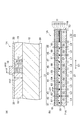
(第1の実施の形態)
図1は、第1実施形態に係る半導体レーザを概略的に示した図である。図1の(a)部は、レーザ共振方向に垂直な方向に沿って表した断面図であり、図1の(b)部は、レーザ共振方向に沿って表した断面図である。
First Embodiment
FIG. 1 is a view schematically showing a semiconductor laser according to the first embodiment. Part (a) of FIG. 1 is a cross-sectional view taken along a direction perpendicular to the laser resonance direction, and part (b) of FIG. 1 is a cross-sectional view taken along the laser resonance direction.
半導体レーザ1Aは、半導体基板10の主面上に設けられた半導体積層11を備える。半導体基板10は、例えば、n型InPからなることができる。このn型InPには、例えば、Siがドープされ、このドーピング濃度は、例えば5×1018cm−3である。半導体積層11には、下部クラッド層12、回折格子層13、埋込層14、光導波路層15、上部クラッド層16、及びコンタクト層17が、この順に設けられる。また、半導体積層11の上には、上部電極18が設けられる。半導体積層11は、例えばメサ構造を有する。このメサ構造の半導体積層11を埋め込むための高抵抗層19が設けられる。高抵抗層19の上には、絶縁層20が設けられる。半導体基板10の下には、下部電極30が設けられる。メサ構造の半導体積層11の厚さH11は、例えば1.5μmであり、メサ幅W11は、例えば1.5μmである。
The semiconductor laser 1 </ b> A includes a
下部クラッド層12は、例えば、n型InPを含む。このn型InPは、半導体基板10の主面上にエピタキシャル成長される。引き続く説明において、半導体積層11の結晶成長には、例えば、分子線エピタキシー(MBE)法又は有機金属気相成長(MOCVD)法などが適用できる。下部クラッド層12のn型InPには、例えば、Siがドープされ、このドーピング濃度は、例えば1×1018cm−3である。下部クラッド層12の厚さは、例えば100nmである。
The
回折格子層13は、例えば、n型Ga0.22In0.78As0.47P0.53などのn型GaInAsPを含む。この回折格子層13は、下部クラッド層12上に成長される。回折格子層13のGaInAsPには、例えば、Siがドープされ、このドーピング濃度は、例えば1×1018cm−3であることができる。回折格子層13の厚さは、例えば60nmである。
The
回折格子層13の上には、埋込層14が成長される。埋込層14は、例えば、n型のInPからなることができる。埋込層14には、例えば、Siがドープされ、このドーピング濃度は、例えば1×1018cm−3である。埋込層14の厚さは、例えば100nmである。埋込層14によって、回折格子層13が平坦化される。
The buried
埋込層14の上には、光導波路層15が成長される。光導波路層15は、例えば、InP基板と格子整合し、フォトルミネッセンス(PL)波長1.55μmで利得を有するInGaAsP量子井戸構造とすることができる。光導波路層15の厚さは、例えば100nmである。
The
光導波路層15の上には、上部クラッド層16が成長される。上部クラッド層16は、例えば、p型InPを含むことができる。上部クラッド層16のp型InPには、例えば、Znがドープされ、このドーピング濃度は、例えば5×1017cm−3である。上部クラッド層16の厚さは、例えば1.0μmである。
An
半導体積層11は、利得を有する第1領域(Sampled-GratingDistributed Feedback Area:SG−DFB領域)21と、第1領域21と光接合される第2領域(Distributed Feedback Area:DFB領域)22とを有し、第1領域21及び第2領域22は、半導体積層11のレーザ共振方向E1に順に配列される。第1領域21は、半導体レーザ1Aの利得領域として機能する。第2領域22は、利得を有する場合と利得を有さない場合の二通りの態様をとることができる。第1実施形態の第2領域22は、利得を有し、半導体レーザ1Aの利得領域として機能する。第1実施形態では、光導波路層15は、第1領域21及び第2領域22において、半導体レーザの活性層としての機能を有する。
The
第1領域21の回折格子層13(第1回折格子層)、及び第2領域22の回折格子層13(第2回折格子層)は、例えば、第1回折格子31及び第2回折格子32(コルゲーション)をそれぞれ有する。第1回折格子31及び第2回折格子32は、例えば回折格子パターンを用いた電子ビーム(Electron Beam:EB) 露光法、或いは二光束干渉露光法により形成される。第2回折格子層13では、第2回折格子32が連続して形成されている。第1回折格子層13は、複数の回折格子部41〜49と、複数の回折格子部41〜49の間に設けられるスペース部とからなる。具体的には、第1回折格子31は、クラッド33と、このクラッド33に設けられた複数の回折格子部41〜49とを有する。回折格子部41〜49は、クラッド33内において、所定の間隔(スペース部)をあけて離散的に配置される。複数の回折格子部41〜49は、レーザ共振方向E1に並んでいる。第1実施形態では、クラッド33には、例えば、9つのセグメント51〜59が設けられ、このセグメント51〜59が、回折格子部41〜49を有する。二光束干渉露光法により第1回折格子31が形成される場合、第1領域21では、回折格子パターンがレジストに露光された後、回折格子が形成されない部分に再度露光が施される。これにより、回折格子が形成されないクラッド33の領域には、回折格子パターンが転写されないようにすることができる。
The diffraction grating layer 13 (first diffraction grating layer) of the
クラッド33は、第1領域21における複数の回折格子部のうち、第2領域22に最も近い回折格子部49と第2領域22との間に第1位相調整部(PS領域)60を有する。第1位相調整部60は、セグメント59に含まれる。
The
第1領域21の回折格子部の回折格子ピッチΛは、2300〜2500Åであり、例えば、2400Åであることができる。回折格子部41〜49の長さ31Lは、10〜30Λであり、例えば、20Λであることができる。その場合、反射結合係数κは150cm−1である。回折格子部の間隔(ピッチ)L1〜L8は、20〜300μm程度の任意の値をとることができる。第1位相調整部60の回折格子部を除いた幅L9は、例えば、60.2μmである。幅L9は、特に制約はないものの、回折格子部の間隔(ピッチ)L1〜L8の長さの2/3以下であることが望ましい。これはL9の長さがL1〜L8に比べて長いと、光が共振器内に閉じこもり、出射効率が低下するためである。
The grating pitch Λ of the grating portion of the
コンタクト層17は、例えば、p型Ga0.47In0.53As結晶によって構成される。コンタクト層17には、例えば、Znがドープされ、このドーピング濃度は、例えば5×1018cm−3である。絶縁層20は、例えば、SiN及びSiO2などの絶縁体からなる保護膜である。上部電極18は、金などの導電性材料からなる。上部電極18は、半導体積層11の第1領域21及び第2領域22の上に設けられ、第1領域21上から第2領域22上に延在する。半導体レーザ1Aは、端面71A及び端面71Aと反対側に位置する端面71Bを有し、端面71A及び端面71Bに、ARコートが設けられる。このARコートは、例えば1.0%程度以下の光反射率を有し、レーザ光が共振器内部から外部に出力されるときの端面71A及び端面71Bでの光反射率を零に近づけることができる。高抵抗層19は、例えばFeドープの半絶縁性InPを含む。
The
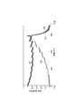
図2は、第1実施形態に係る第2領域22の反射スペクトルを示した図である。この反射スペクトルは、第2領域22の外部から第2領域22に入射した光の反射特性を表す。第2領域22の回折格子部の回折格子ピッチΛは、第1領域21の回折格子部の回折格子ピッチΛと同じである。すなわち、第2領域22の回折格子部の回折格子ピッチΛは、2300〜2500Åであり、例えば、2400Åであることができる。第2領域22の第2回折格子層の長さL32は、例えば120μmであり、反射結合係数κは、第1領域21の反射結合係数κと同じである。この反射スペクトルは、5.5nmの反射帯域幅B1を有する。反射帯域幅とは、例えば、−3dB反射帯域幅のことをいう。
FIG. 2 is a diagram showing a reflection spectrum of the
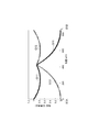
図3は、第1実施形態に係る利得スペクトルと反射スペクトルとを示した図である。図3の(a)部は、利得スペクトルのピーク間隔が反射スペクトルの反射帯域幅より大きい実施例を表す。回折格子部の間隔(ピッチ)L1〜L8は、それらの全てが、例えば50μm又はその近傍の値を有する。図3の(a)部では、利得スペクトルのピーク間隔は6.0nmであり、反射スペクトルの反射帯域幅の5.5nmより大きいので、反射帯域内に利得スペクトルピークが一つのみ存在するように利得スペクトルのシフトが可能である。反射スペクトルの反射帯域幅の中に、利得スペクトルピークが一つのみ存在すると、半導体レーザ1Aは安定的に単一波長でのレーザ発振を行うことができる。利得スペクトルピークが二つ以上存在すると、半導体レーザ1Aのレーザ発振は不安定となる。第1実施形態では、第2位相調整部61〜68(図1の(b)部を参照)により任意の位相シフトを与えることによって、利得スペクトルピークが反射スペクトルの反射帯域の中心付近に存在するように利得スペクトルをシフトさせることが可能である。第2位相調整部61〜68は、隣り合う回折格子部の間に設けられる。第2位相調整部61〜68の位相シフト量の調整は、導波路幅調整による等価位相シフト、又は、回折格子を描画する際に描画位置をずらす物理的シフトによって行うことができる。
FIG. 3 is a diagram showing a gain spectrum and a reflection spectrum according to the first embodiment. Part (a) of FIG. 3 represents an embodiment in which the peak interval of the gain spectrum is larger than the reflection bandwidth of the reflection spectrum. The intervals (pitches) L1 to L8 of the diffraction grating portion all have values of, for example, 50 μm or its vicinity. In part (a) of FIG. 3, the peak interval of the gain spectrum is 6.0 nm, which is larger than 5.5 nm of the reflection bandwidth of the reflection spectrum, so that only one gain spectrum peak is present in the reflection band. Shifting of the gain spectrum is possible. When only one gain spectrum peak is present in the reflection bandwidth of the reflection spectrum, the
図3の(b)部は、利得スペクトルのピーク間隔が反射スペクトルの反射帯域幅の80%以上であり、かつ、反射帯域幅より小さい実施例を表す。回折格子部の間隔(ピッチ)L1〜L8は、それらの全てが、例えば65μm又はその近傍の値を有する。図3の(b)部では、利得スペクトルのピーク間隔は5.0nmであり、反射スペクトルの反射帯域幅の5.5nmに比べて10%小さい。利得スペクトルのピーク間隔が反射スペクトルの反射帯域幅に比べて小さいので、利得スペクトルピークが、反射スペクトルの反射帯域内に2つ存在し得る。ただし、図3の(b)部では、例えば公差によって一の利得スペクトルピークがシフトした結果、その一の利得スペクトルピークが反射スペクトルの反射帯域外となっても、別の利得スペクトルピークが、反射スペクトルの反射帯域内に存在するようにシフトできる。このシフトは、図3の(a)部と同様に、第2位相調整部61〜68によって任意の位相シフトを与えることにより行うことができる。第1実施形態では、利得スペクトルのピーク間隔が反射スペクトルの反射帯域幅に比べて10%程度小さいことがより好ましい。
Part (b) of FIG. 3 represents an embodiment in which the peak interval of the gain spectrum is 80% or more of the reflection bandwidth of the reflection spectrum and smaller than the reflection bandwidth. The intervals (pitches) L1 to L8 of the diffraction grating portion all have values of, for example, 65 μm or its vicinity. In part (b) of FIG. 3, the peak interval of the gain spectrum is 5.0 nm, which is 10% smaller than the reflection bandwidth of 5.5 nm of the reflection spectrum. Since the peak spacing of the gain spectrum is small compared to the reflection bandwidth of the reflection spectrum, two gain spectrum peaks may be present in the reflection band of the reflection spectrum. However, in part (b) of FIG. 3, for example, as a result of one gain spectrum peak shifting due to tolerance, another gain spectrum peak is reflected even if the one gain spectrum peak falls outside the reflection band of the reflection spectrum. It can be shifted to lie within the reflection band of the spectrum. Similar to the part (a) of FIG. 3, this shift can be performed by giving an arbitrary phase shift by the
図4は、図3の(b)部において、第1位相調整部60に位相シフトを与えたときの半導体レーザの発振スペクトルを示す図である。第1位相調整部60の位相シフト量は、−0.4π(rad)、又は、回折格子ピッチをΛ(nm)とすると0.4Λ(nm)である。図4に示されるように、半導体レーザ1Aは、波長1550nm近傍の単一波長で安定的に発振する。第1位相調整部60での位相シフトは、等価位相シフトあるいは描画位置シフトによる行うことができる。第1位相調整部60の位相シフト量は、第2位相調整部61〜68の位相シフト量と異なることができる。
FIG. 4 is a diagram showing an oscillation spectrum of the semiconductor laser when a phase shift is given to the first
図5は、第1実施形態に係る半導体レーザ1Aの共振器内における光電界強度分布を示す図である。なお、図5は、半導体レーザ1Aが、図4の発振スペクトルを有する場合を示している。図5に示されるように、前進波G1は、端面71Aから高い光強度を有して出力される一方で、端面71Bからは殆ど出力されない。後退波G2は、端面71Aから殆ど出力されず、また、端面71Bからも、わずかに出力されるのみである。端面71Aでの前進波G1の光出力強度と、端面71Bでの後退波G2の光出力強度との比は、約95:5である。
FIG. 5 is a view showing an optical electric field strength distribution in the resonator of the
以上に説明した半導体レーザ1Aによって得られる効果について説明する。本実施形態の半導体レーザ1Aによれば、第1回折格子31のスペース部分の長さを調整することで、第2領域22における反射スペクトルの反射帯域の中に、第1領域21における利得スペクトルが一つのみ存在するように構成することができる。第1回折格子31の結合反射率は回折格子が部分的にしか形成されていないため第2領域22よりも低くなり、その結果、第1領域21の出射端面(前端面)から高い光出力を得ることができる。
The effects obtained by the
また、この半導体レーザ1Aでは、第1回折格子31の複数の回折格子部が互いに間隔をあけてレーザ共振方向に並んでいる。ところで、端面からの光出力強度は、反射結合係数κとレーザ共振器長Lの積(κL)によって決められる。ここで、κL値は、単純なファブリ・ペローレーザ(Fabry-Perot Laser Diode:FP−LD)における端面反射率に相当する指標であり、κL値が小さいと端面での反射率が低くなり、κLが大きいと端面での反射率が高くなる。半導体レーザ1Aでは、上述した第1回折格子31の構成によって、前進波G1に対して、端面71AのκL値が端面71BのκL値よりも小さいので、前進波G1の端面71A及び端面71Bの光出力強度の差が生じている。すなわち、前進波G1では、二つの端面71A及び71Bのうち、一方の端面71Aにのみ高い光出力が得られている。後退波G2に対しては、端面71A及び端面71Bにおいて、反射率が高くなるようにκL値が設定され、その結果、端面71A及び端面71Bでの光出力強度が共に抑えられる。従って、この半導体レーザ1Aによれば、そのレーザ出力を実質的に一の端面71Aに限ることができ、その結果、高い光出力を得ることができる。さらに、この半導体レーザ1Aでは、第1領域21に回折格子部が設けられるので、回折格子の全体の本数が少なくなり、半導体レーザ製造の安定性に優れる。
Further, in the
単純なFP−LDにおいてレーザ光の高出力が行われるときは、例えば、一端面の反射率を低くし、この反対側に位置する他端面の反射率を高くする、 いわゆるLR−HRの形態がよく用いられる。 When high output of laser light is performed in a simple FP-LD, for example, the form of so-called LR-HR, which reduces the reflectance of one end surface and increases the reflectance of the other end surface located on the opposite side, is It is often used.
一方、回析格子の中心部分にλ/4位相シフト領域を有するDFBレーザでは、特殊な製造法を採らない限り、一様な反射結合係数κを持つ導波路が形成されるので、FP−LDのように、二つの端面の反射率を互いに変えるようなことが困難である。二つの端面の反射率を変えるために、回析格子の中心部分にλ/4位相シフト領域の位置を中心から移動させるという手法が採られることもある。しかしこの手法では、レーザ光のスペクトル形状の劣化を招くので、たとえば高い単一モード性が要求される製品用途には不向きとなる。したがってこの場合、λ/4位相シフトは回析格子の中心部に設けざるを得ず、結果として前後端面から同等強度の光を出射されることになり、効率的な光出力が難しい。本実施形態の半導体レーザ1Aでは、従来のDFBレーザのような一様に回折格子を形成した構造は採られていない。
On the other hand, in a DFB laser having a λ / 4 phase shift region in the central part of the diffraction grating, a waveguide having a uniform reflection coupling coefficient 形成 is formed unless a special manufacturing method is adopted, so that FP-LD It is difficult to change the reflectances of the two end faces with each other. In order to change the reflectivity of the two end faces, a method may be employed in which the position of the λ / 4 phase shift region is moved from the center at the central portion of the diffraction grating. However, this method causes degradation of the spectral shape of the laser light, and is therefore unsuitable for use in, for example, product applications where high single mode characteristics are required. Therefore, in this case, the λ / 4 phase shift must be provided at the central portion of the diffraction grating, and as a result, light of equal intensity is emitted from the front and rear end faces, and efficient light output is difficult. In the
本構造はレーザ線幅特性においても有利である。近年、光通信システム技術の向上に伴い、狭線幅レーザ特性が求められている。レーザ線幅は、レーザ共振器内のフォトン数に反比例するので、狭線幅特性を得るには、フォトン数が多くなる長い共振器構造のレーザが有利である。一般に長共振器のDFBレーザを安定性良く製造するのは難しい。DFBレーザは、反射結合係数κが小さいと閾値電流が増し、κが高いと光が取り出しにくくなる性質がある。そのためκには最適値が存在し、製造上管理が必要となるが、共振器が長いとそのばらつき許容範囲が狭くなる。これに対し本実施形態の半導体レーザ1Aは、共振器を長くとっても光が閉じこもることはないため、κの繊細な管理が不要であり、それゆえ線幅に有利な共振器の長尺化も容易に行うことができる。
The present structure is also advantageous in laser linewidth characteristics. In recent years, narrow line width laser characteristics are required with the improvement of optical communication system technology. Since the laser line width is inversely proportional to the number of photons in the laser resonator, a laser with a long resonator structure with a large number of photons is advantageous to obtain narrow line width characteristics. In general, it is difficult to stably manufacture a long cavity DFB laser. The DFB laser has a property that the threshold current increases when the reflection coupling coefficient κ is small, and the light is difficult to extract when κ is high. Therefore, an optimum value exists for κ, and management in manufacturing is required, but if the resonator is long, the variation tolerance range becomes narrow. On the other hand, the
また、この半導体レーザ1Aでは、第2領域は、利得を有することが好ましい。この半導体レーザによれば、第2領域は反射器として機能する。そのため第2領域は利得導波路である必要はないが、大きな損失が生じるような構成は避けなければならない。これを実現する最も簡便な方法は、第1領域と第2領域とを同一材料で形成し、一つの電極で利得を与えるという形態である。第2領域を第1領域とは異なる材料で構成する形態も可能だが、異なる材料を形成させる工程で複雑さが生じる。このような半導体レーザ1Aによれば、第1領域21に加えて、第2領域22が利得を有するので、よりレーザ出力を向上させることができる。また、第1領域21と第2領域22とを、例えばバットジョイント法を用いることなく共通の半導体層によって形成できるので、製造工程を少なくできる。
In the
また、上記の半導体レーザ1Aのように、第1領域の利得スペクトルのピーク間隔は、第2領域の反射帯域幅より大きいことが好ましい。この半導体レーザでは、第1領域で生成される複数の利得スペクトルの波長ピークのうち第2領域の反射帯域にある波長のみが選択されて発振する。したがって安定した単一モード発振を得るためには、第2反射帯域に一つの利得スペクトルの波長ピークが潜在する形態が望ましい。その点で第1領域のモード間隔は、第2領域の反射帯域より広く設計するのが好ましい。
Further, as in the above-described
また、この半導体レーザ1Aでは、第1領域の利得スペクトルのピーク間隔は、第2領域の反射スペクトルの反射帯域幅の80%以上であり、かつ、該反射帯域幅より小さいことが好ましい。前述の利得スペクトルの波長ピーク間隔が、第2領域の反射帯域に比べあまりに広いと、場合によっては第2領域の反射帯域に利得スペクトルの波長ピークが合致しないという事態が生じ得る。第2領域の中心反射波長は第2領域回折格子のブラグ波長である。この波長は回折格子ピッチで決まるため、製造ばらつきはほとんどない。一方第1領域の利得スペクトルの波長ピークは、前記回折格子部の間隔の光路長によって決まる。この光路長は、等価屈折率の違いなどでややばらつきが大きい。そこで利得スペクトルの波長ピークの波長がばらついても、常に安定した単一モードが実現できるよう、第1領域の利得スペクトルのピーク間隔を、第2領域の反射スペクトルの反射帯域幅の80%以上、かつ、該反射帯域幅より小さくなるよう、前記第1領域の回折格子部の間隔を設定するのが好ましい。この場合、利得スペクトルのピーク間隔が反射スペクトルの反射帯域幅より狭いため、利得スペクトルピークが、反射スペクトルの反射帯域内に2つ存在する場合が生じ得るが、第2領域の反射スペクトル強度が、これら2つの波長で全く等しくなる場合を除き、高歩留りで単一モード発振する素子を得ることができる。
In the
また、本実施形態の半導体レーザ1Aのように、第1領域21の複数の回折格子部のうち第2領域22に最も近い回折格子部49と第2領域22との間に第1位相調整部60が設けられることが好ましい。この半導体レーザによれば、第1位相調整部60によって、発振状態を良好にすることができる。第1位相調整部60の位相調整は、第1領域21と第2領域22の反射位相整合に寄与し、低閾値特性を可能とする。
Further, as in the
また、本実施形態の半導体レーザ1Aのように、隣り合う回折格子部の間に第2位相調整部61〜68が設けられることが好ましい。この半導体レーザ1Aによれば、第1領域21における利得スペクトル全体がシフトするので、反射スペクトルの反射帯域内(好ましくは反射帯域の中心付近)に利得スペクトルピークが一つのみ存在するように、反射スペクトルと利得スペクトルとの関係を好適に調整することが可能となる。
Further, as in the
また、本実施形態の半導体レーザ1Aでは、第1位相調整部60の位相シフト量は、第2位相調整部61〜68の位相シフト量と異なってもよい。この半導体レーザ1Aによれば、第1位相調整部60及び第2位相調整部61〜68において、それぞれの領域に好適な位相シフト量を実現することができる。
Further, in the
半導体レーザ1Aでは、半導体積層11の第1領域21上から第2領域22上に延在する上部電極18を備えてもよい。この半導体レーザ1Aによれば、一つの上部電極18により、第1領域21及び第2領域22に電圧を印加して、半導体レーザ1Aが単一波長でレーザ発振するように制御できる。
The semiconductor laser 1 </ b> A may include an
(第2の実施の形態)
図6は、第2実施形態に係る半導体レーザをレーザ共振方向に沿って概略的に表した断面図である。第2実施形態に係る半導体レーザ1Bでは、第1実施形態に係る半導体レーザ1Aに対し、上部電極の構造が異なっている。すなわち、第2実施形態の半導体レーザ1Bは、第1領域21及び第2領域22それぞれに、互いに分離された上部電極18A及び上部電極18Bそれぞれを有する。第2領域22は、第1実施形態と同様に、利得を有する。
Second Embodiment
FIG. 6 is a cross-sectional view schematically showing the semiconductor laser according to the second embodiment along the laser resonant direction. The
第2実施形態では、第1領域21及び第2領域22のそれぞれに上部電極18A及び上部電極18Bを有するので、第1領域21及び第2領域22のそれぞれに、より適切な電圧を個別に印加することができる。例えば、第2領域22は第1領域21に比べて電流注入量に対する出射効率が低いので、第2領域22は透明程度の電流注入条件にしておき、第1領域21に大電流を流すことで、効率のよいレーザ出射が可能となる。
In the second embodiment, since the upper electrode 18A and the upper electrode 18B are provided in each of the
なお、第1領域21に設けられた上部電極18Aを更に分割して、第1位相調整部60上に独立した上部電極を設けることも可能である。これにより、第1位相調整部60の等価屈折率を変化させて第1領域21と第2領域22の反射位相整合を最適化することができる。
It is also possible to further divide the upper electrode 18A provided in the
(第3の実施の形態)
図7は、第3実施形態に係る半導体レーザをレーザ共振方向に沿って概略的に表した断面図である。第3実施形態に係る半導体レーザ1Cでは、第1実施形態に係る半導体レーザ1Aに対し、上部電極の構成が異なっている。すなわち、第3実施形態の半導体レーザ1Cは、第1領域21にのみ上部電極18Aを有し、第2領域22には上部電極を有さない。第2領域22は、第1実施形態と異なり、利得を有さない。このため、第2領域22は、分布反射型(Distributed Bragg Reflector:DBR)デバイスとしての機能のみを有する。第2領域22は、第1領域21のDFBレーザが単一波長でレーザ発振できるような反射スペクトル(例えば図2を参照)を生成する。
Third Embodiment
FIG. 7 is a cross-sectional view schematically showing the semiconductor laser according to the third embodiment along the laser resonant direction. The
(第4の実施の形態)
図8は、第4実施形態に係る半導体レーザアレイを含むレーザ光源を概略的に示した図である。レーザ光源2は、半導体レーザアレイ3、光合波器4、及び光導波路5を含む。半導体レーザアレイ3は、光合波器4に光学的に結合され、また、光合波器4を介して、光導波路5に光学的に結合される。半導体レーザアレイ3は、共通の半導体基板上において、レーザ共振方向E1と交差する方向E2に複数の半導体レーザが配列されて成ることができ、例えば12本の半導体レーザの配列からなることができる。第4実施形態の半導体レーザは、第1実施形態の半導体レーザと同様の構成を有する。半導体レーザアレイ3は、主に前進波が出力される端面(図1の(b)部での端面71Aに相当する)を揃えて光合波器4に結合される。光合波器4は、例えば12×1のマルチモード干渉(MMI)導波路であることができる。光導波路5は、例えば、半導体光増幅器(Semiconductor Optical Amplifier:SOA)を備えることができる。
Fourth Embodiment
FIG. 8 is a view schematically showing a laser light source including the semiconductor laser array according to the fourth embodiment. The
半導体レーザアレイ3では、例えば12本の半導体レーザが配置されるので、例えば、いずれかの一の半導体レーザにレーザ発振のための電流が加えられると、その一の半導体レーザから、ある単一波長のレーザ光が高出力に得られる。また、別の一の半導体レーザにレーザ発振のための電流が加えられると、その別の半導体レーザから、別の単一波長のレーザ光が高出力に得られる。第1実施形態と同様に高出力化されたレーザ光R1は、第4実施形態では、光合波器4を通して、光導波路5から出力される。光導波路5がSOAを備えると、更に高光強度のレーザ光R1が光導波路5から出力される。
In the semiconductor laser array 3, for example, twelve semiconductor lasers are disposed, so that, for example, when a current for laser oscillation is applied to any one of the semiconductor lasers, a single wavelength from the one semiconductor laser Laser light is obtained at high output. In addition, when a current for laser oscillation is applied to another semiconductor laser, another single wavelength laser beam can be obtained with high output from the other semiconductor laser. In the fourth embodiment, the laser beam R <b> 1 whose output is increased as in the first embodiment is output from the
本発明に係る半導体レーザアレイ3によれば、複数の半導体レーザが備えられ、この複数の半導体レーザは、それぞれ異なる回折格子ピッチを有することができる。このため、一の半導体レーザアレイ3により、半導体レーザの個数に比例して発振波長を拡大できる。 According to the semiconductor laser array 3 of the present invention, a plurality of semiconductor lasers are provided, and the plurality of semiconductor lasers can have different grating pitches. Therefore, the oscillation wavelength can be expanded in proportion to the number of semiconductor lasers by one semiconductor laser array 3.
(比較例)
図9は、比較例に係る利得スペクトルと反射スペクトルの反射帯域幅とを示した図である。図9は、利得スペクトルのピーク間隔が反射スペクトルの反射帯域幅の80%未満である例を表す。回折格子部の間隔(ピッチ)L1〜L8は、それらの全てが、例えば65μm又はその近傍の値を有する。半導体レーザの構成は、回折格子部の間隔(ピッチ)L1〜L8を除いて、第1実施形態の図1と同様である。図9では、利得スペクトルのピーク間隔が、反射スペクトルの反射帯域幅の5.5nmに比べて小さい。従って、利得スペクトルピークが、反射スペクトルの反射帯域内に常時二つ存在し得る。このため、二以上の波長のレーザ光が第2領域22によって反射されるので、半導体レーザのレーザ発振が不安定となる。
(Comparative example)
FIG. 9 is a diagram showing the gain spectrum and the reflection bandwidth of the reflection spectrum according to the comparative example. FIG. 9 represents an example where the peak spacing of the gain spectrum is less than 80% of the reflection bandwidth of the reflection spectrum. The intervals (pitches) L1 to L8 of the diffraction grating portion all have values of, for example, 65 μm or its vicinity. The configuration of the semiconductor laser is the same as that of FIG. 1 of the first embodiment except for the intervals (pitch) L1 to L8 of the diffraction grating portion. In FIG. 9, the peak interval of the gain spectrum is smaller than 5.5 nm of the reflection bandwidth of the reflection spectrum. Thus, two gain spectrum peaks can always be present in the reflection band of the reflection spectrum. For this reason, since laser light of two or more wavelengths is reflected by the
以上、好適な実施の形態において本発明の原理を図示し説明してきたが、本発明は、そのような原理から逸脱することなく配置及び詳細において変更され得ることは、当業者によって認識される。本発明は、本実施の形態に開示された特定の構成に限定されるものではない。したがって、特許請求の範囲及びその精神の範囲から来る全ての修正及び変更に権利を請求する。 While the principles of the present invention have been illustrated and described in the preferred embodiment, it will be appreciated by those skilled in the art that the present invention can be modified in arrangement and detail without departing from such principles. The present invention is not limited to the specific configuration disclosed in the present embodiment. Therefore, we claim all modifications and changes coming from the scope of claims and the scope of the spirit thereof.
本発明によれば、単一波長でレーザ発振するとともに、出力光強度を向上できる半導体レーザ及び半導体レーザアレイが提供される。 According to the present invention, there are provided a semiconductor laser and a semiconductor laser array capable of performing laser oscillation with a single wavelength and improving the output light intensity.
1A、1B、1C…半導体レーザ、3…半導体レーザアレイ、10…半導体基板、11…半導体積層、13…回折格子層、18…上部電極、21…第1領域、22…第2領域、31…第1回折格子、32…第2回折格子、41〜49…回折格子部、60…第1位相調整部、61〜68…第2位相調整部、E1…レーザ共振方向。
DESCRIPTION OF
Claims (2)
利得を有し、複数の回折格子部と前記複数の回折格子部の間に設けられるスペース部とからなる第1回折格子層を有する第1領域と、
前記第1領域と光接合され、回折格子が一定のピッチで連続して形成される第2回折格子層を有する第2領域と、
前記第1領域上のみに延在する上部電極と、
を備え、
前記第1領域の利得スペクトルのピーク間隔は、前記第2領域の反射スペクトルの反射帯域幅の80%以上である、半導体レーザ。 Provided on the main surface of the semiconductor substrate,
A first region having a first diffraction grating layer having a gain and comprising a plurality of diffraction grating portions and a space portion provided between the plurality of diffraction grating portions;
Wherein the first region and a light junction, a second region where the diffraction grating is have a second diffraction grating layer which is formed continuously at a constant pitch,
An upper electrode extending only on the first region;
Equipped with
The semiconductor laser , wherein the peak interval of the gain spectrum of the first region is 80% or more of the reflection bandwidth of the reflection spectrum of the second region .
Priority Applications (2)
| Application Number | Priority Date | Filing Date | Title |
|---|---|---|---|
| JP2014245704A JP6507604B2 (en) | 2014-12-04 | 2014-12-04 | Semiconductor laser and semiconductor laser array |
| US14/959,782 US20160164249A1 (en) | 2014-12-04 | 2015-12-04 | Semiconductor laser diode and laser array implementing the same |
Applications Claiming Priority (1)
| Application Number | Priority Date | Filing Date | Title |
|---|---|---|---|
| JP2014245704A JP6507604B2 (en) | 2014-12-04 | 2014-12-04 | Semiconductor laser and semiconductor laser array |
Publications (3)
| Publication Number | Publication Date |
|---|---|
| JP2016111118A JP2016111118A (en) | 2016-06-20 |
| JP2016111118A5 JP2016111118A5 (en) | 2017-10-26 |
| JP6507604B2 true JP6507604B2 (en) | 2019-05-08 |
Family
ID=56095183
Family Applications (1)
| Application Number | Title | Priority Date | Filing Date |
|---|---|---|---|
| JP2014245704A Active JP6507604B2 (en) | 2014-12-04 | 2014-12-04 | Semiconductor laser and semiconductor laser array |
Country Status (2)
| Country | Link |
|---|---|
| US (1) | US20160164249A1 (en) |
| JP (1) | JP6507604B2 (en) |
Family Cites Families (14)
| Publication number | Priority date | Publication date | Assignee | Title |
|---|---|---|---|---|
| GB2381123B (en) * | 2001-10-17 | 2005-02-23 | Marconi Optical Components Ltd | Tuneable laser |
| US6763165B1 (en) * | 2002-01-15 | 2004-07-13 | Adc Telecommunications, Inc. | Grating assisted coupler with controlled start |
| JP4288953B2 (en) * | 2002-02-19 | 2009-07-01 | 三菱電機株式会社 | Tunable semiconductor laser |
| JP2005317695A (en) * | 2004-04-28 | 2005-11-10 | Furukawa Electric Co Ltd:The | Laser device |
| JP4657853B2 (en) * | 2005-08-11 | 2011-03-23 | 住友電工デバイス・イノベーション株式会社 | Semiconductor laser, laser module, optical component, laser device, semiconductor laser manufacturing method, and semiconductor laser control method |
| EP2174392B1 (en) * | 2007-08-02 | 2020-04-29 | EFFECT Photonics B.V. | Semiconductor laser device |
| JP5058087B2 (en) * | 2008-07-10 | 2012-10-24 | 三菱電機株式会社 | Tunable semiconductor laser |
| JP5287460B2 (en) * | 2009-04-17 | 2013-09-11 | 富士通株式会社 | Semiconductor laser |
| JP5625459B2 (en) * | 2009-05-21 | 2014-11-19 | 住友電気工業株式会社 | Semiconductor laser device and manufacturing method thereof |
| JP2011119434A (en) * | 2009-12-03 | 2011-06-16 | Renesas Electronics Corp | Semiconductor laser device and method of manufacturing the same |
| JP2011253977A (en) * | 2010-06-03 | 2011-12-15 | Mitsubishi Electric Corp | Dbr laser |
| JP2013077645A (en) * | 2011-09-29 | 2013-04-25 | Sumitomo Electric Device Innovations Inc | Semiconductor laser and control method of the same |
| JP6186864B2 (en) * | 2012-05-18 | 2017-08-30 | 住友電気工業株式会社 | Semiconductor laser |
| JP5692330B2 (en) * | 2013-10-18 | 2015-04-01 | 住友電気工業株式会社 | Wavelength tunable laser, wavelength tunable laser apparatus, and wavelength tunable laser control method |
-
2014
- 2014-12-04 JP JP2014245704A patent/JP6507604B2/en active Active
-
2015
- 2015-12-04 US US14/959,782 patent/US20160164249A1/en not_active Abandoned
Also Published As
| Publication number | Publication date |
|---|---|
| US20160164249A1 (en) | 2016-06-09 |
| JP2016111118A (en) | 2016-06-20 |
Similar Documents
| Publication | Publication Date | Title |
|---|---|---|
| US9312663B2 (en) | Laser device, light modulation device, and optical semiconductor device | |
| US10770863B2 (en) | Semiconductor laser device | |
| JP4954992B2 (en) | Semiconductor light reflecting element, semiconductor laser using the semiconductor light reflecting element, and optical transponder using the semiconductor laser | |
| WO2009116140A1 (en) | Optical semiconductor element and its manufacturing method | |
| JP5182362B2 (en) | Optical element and manufacturing method thereof | |
| JP2011204895A (en) | Semiconductor laser | |
| JP6510391B2 (en) | Semiconductor laser | |
| US9172212B2 (en) | Tunable semiconductor laser diode | |
| JP6588859B2 (en) | Semiconductor laser | |
| JP3682367B2 (en) | Distributed feedback laser diode | |
| US7949020B2 (en) | Semiconductor laser and optical integrated semiconductor device | |
| JP2014017347A (en) | Semiconductor laser | |
| JP4926641B2 (en) | Semiconductor laser | |
| JP5310533B2 (en) | Optical semiconductor device | |
| JP2003289169A (en) | Semiconductor laser | |
| JP6588858B2 (en) | Semiconductor laser | |
| JP2018098419A (en) | Semiconductor laser, light source unit, communication system, and wavelength multiplex optical communication system | |
| JP2013219192A (en) | Semiconductor laser | |
| JP2009054721A (en) | Semiconductor element, and manufacturing method of semiconductor element | |
| JP6507604B2 (en) | Semiconductor laser and semiconductor laser array | |
| JP5272859B2 (en) | Semiconductor laser element | |
| JP5058087B2 (en) | Tunable semiconductor laser | |
| JP2003218462A (en) | Distributed feedback semiconductor laser device | |
| JP2003152272A (en) | Dispersed phase shift structure distributed feedback semiconductor laser | |
| JP2004273644A (en) | Semiconductor laser |
Legal Events
| Date | Code | Title | Description |
|---|---|---|---|
| A521 | Request for written amendment filed |
Free format text: JAPANESE INTERMEDIATE CODE: A523 Effective date: 20170912 |
|
| A621 | Written request for application examination |
Free format text: JAPANESE INTERMEDIATE CODE: A621 Effective date: 20170912 |
|
| A977 | Report on retrieval |
Free format text: JAPANESE INTERMEDIATE CODE: A971007 Effective date: 20180731 |
|
| A131 | Notification of reasons for refusal |
Free format text: JAPANESE INTERMEDIATE CODE: A131 Effective date: 20180807 |
|
| A601 | Written request for extension of time |
Free format text: JAPANESE INTERMEDIATE CODE: A601 Effective date: 20181005 |
|
| A521 | Request for written amendment filed |
Free format text: JAPANESE INTERMEDIATE CODE: A523 Effective date: 20181112 |
|
| TRDD | Decision of grant or rejection written | ||
| A01 | Written decision to grant a patent or to grant a registration (utility model) |
Free format text: JAPANESE INTERMEDIATE CODE: A01 Effective date: 20190305 |
|
| A61 | First payment of annual fees (during grant procedure) |
Free format text: JAPANESE INTERMEDIATE CODE: A61 Effective date: 20190318 |
|
| R150 | Certificate of patent or registration of utility model |
Ref document number: 6507604 Country of ref document: JP Free format text: JAPANESE INTERMEDIATE CODE: R150 |
|
| R250 | Receipt of annual fees |
Free format text: JAPANESE INTERMEDIATE CODE: R250 |
|
| R250 | Receipt of annual fees |
Free format text: JAPANESE INTERMEDIATE CODE: R250 |
|
| R250 | Receipt of annual fees |
Free format text: JAPANESE INTERMEDIATE CODE: R250 |