JP6503334B2 - Copper pillar mounting board - Google Patents
Copper pillar mounting board Download PDFInfo
- Publication number
- JP6503334B2 JP6503334B2 JP2016500941A JP2016500941A JP6503334B2 JP 6503334 B2 JP6503334 B2 JP 6503334B2 JP 2016500941 A JP2016500941 A JP 2016500941A JP 2016500941 A JP2016500941 A JP 2016500941A JP 6503334 B2 JP6503334 B2 JP 6503334B2
- Authority
- JP
- Japan
- Prior art keywords
- traces
- solder resist
- assembly
- layer
- trace
- Prior art date
- Legal status (The legal status is an assumption and is not a legal conclusion. Google has not performed a legal analysis and makes no representation as to the accuracy of the status listed.)
- Active
Links
- 239000010949 copper Substances 0.000 title claims description 39
- RYGMFSIKBFXOCR-UHFFFAOYSA-N Copper Chemical compound [Cu] RYGMFSIKBFXOCR-UHFFFAOYSA-N 0.000 title claims description 37
- 229910052802 copper Inorganic materials 0.000 title claims description 37
- 229910000679 solder Inorganic materials 0.000 claims description 106
- 239000000758 substrate Substances 0.000 claims description 48
- 238000000034 method Methods 0.000 claims description 13
- 239000004020 conductor Substances 0.000 claims description 9
- ATJFFYVFTNAWJD-UHFFFAOYSA-N Tin Chemical compound [Sn] ATJFFYVFTNAWJD-UHFFFAOYSA-N 0.000 claims description 4
- 239000010410 layer Substances 0.000 claims 26
- 239000011247 coating layer Substances 0.000 claims 10
- 238000000576 coating method Methods 0.000 description 10
- 239000011248 coating agent Substances 0.000 description 9
- 239000004065 semiconductor Substances 0.000 description 5
- 235000012431 wafers Nutrition 0.000 description 4
- 239000002184 metal Substances 0.000 description 3
- 229910052751 metal Inorganic materials 0.000 description 3
- 229910052709 silver Inorganic materials 0.000 description 3
- 239000004332 silver Substances 0.000 description 3
- XUIMIQQOPSSXEZ-UHFFFAOYSA-N Silicon Chemical compound [Si] XUIMIQQOPSSXEZ-UHFFFAOYSA-N 0.000 description 2
- 230000007547 defect Effects 0.000 description 2
- 238000013461 design Methods 0.000 description 2
- PCHJSUWPFVWCPO-UHFFFAOYSA-N gold Chemical compound [Au] PCHJSUWPFVWCPO-UHFFFAOYSA-N 0.000 description 2
- 229910052737 gold Inorganic materials 0.000 description 2
- 239000010931 gold Substances 0.000 description 2
- 238000010438 heat treatment Methods 0.000 description 2
- 239000000463 material Substances 0.000 description 2
- 229910052710 silicon Inorganic materials 0.000 description 2
- 239000010703 silicon Substances 0.000 description 2
- 229910045601 alloy Inorganic materials 0.000 description 1
- 239000000956 alloy Substances 0.000 description 1
- 230000015572 biosynthetic process Effects 0.000 description 1
- 238000010586 diagram Methods 0.000 description 1
- 230000000694 effects Effects 0.000 description 1
- 239000011810 insulating material Substances 0.000 description 1
- 238000004519 manufacturing process Methods 0.000 description 1
- 238000002844 melting Methods 0.000 description 1
- 230000008018 melting Effects 0.000 description 1
- 238000013508 migration Methods 0.000 description 1
- 230000005012 migration Effects 0.000 description 1
- 239000000203 mixture Substances 0.000 description 1
- 238000012986 modification Methods 0.000 description 1
- 230000004048 modification Effects 0.000 description 1
- 239000012811 non-conductive material Substances 0.000 description 1
- 238000013021 overheating Methods 0.000 description 1
- 230000003071 parasitic effect Effects 0.000 description 1
- 238000002161 passivation Methods 0.000 description 1
- 230000008092 positive effect Effects 0.000 description 1
Images


Classifications
-
- H—ELECTRICITY
- H01—ELECTRIC ELEMENTS
- H01L—SEMICONDUCTOR DEVICES NOT COVERED BY CLASS H10
- H01L21/00—Processes or apparatus adapted for the manufacture or treatment of semiconductor or solid state devices or of parts thereof
- H01L21/02—Manufacture or treatment of semiconductor devices or of parts thereof
- H01L21/04—Manufacture or treatment of semiconductor devices or of parts thereof the devices having at least one potential-jump barrier or surface barrier, e.g. PN junction, depletion layer or carrier concentration layer
- H01L21/48—Manufacture or treatment of parts, e.g. containers, prior to assembly of the devices, using processes not provided for in a single one of the subgroups H01L21/06 - H01L21/326
- H01L21/4814—Conductive parts
- H01L21/4846—Leads on or in insulating or insulated substrates, e.g. metallisation
- H01L21/4853—Connection or disconnection of other leads to or from a metallisation, e.g. pins, wires, bumps
-
- H—ELECTRICITY
- H01—ELECTRIC ELEMENTS
- H01L—SEMICONDUCTOR DEVICES NOT COVERED BY CLASS H10
- H01L24/00—Arrangements for connecting or disconnecting semiconductor or solid-state bodies; Methods or apparatus related thereto
- H01L24/01—Means for bonding being attached to, or being formed on, the surface to be connected, e.g. chip-to-package, die-attach, "first-level" interconnects; Manufacturing methods related thereto
- H01L24/10—Bump connectors ; Manufacturing methods related thereto
- H01L24/11—Manufacturing methods
-
- H—ELECTRICITY
- H01—ELECTRIC ELEMENTS
- H01L—SEMICONDUCTOR DEVICES NOT COVERED BY CLASS H10
- H01L23/00—Details of semiconductor or other solid state devices
- H01L23/48—Arrangements for conducting electric current to or from the solid state body in operation, e.g. leads, terminal arrangements ; Selection of materials therefor
- H01L23/488—Arrangements for conducting electric current to or from the solid state body in operation, e.g. leads, terminal arrangements ; Selection of materials therefor consisting of soldered or bonded constructions
- H01L23/498—Leads, i.e. metallisations or lead-frames on insulating substrates, e.g. chip carriers
- H01L23/49838—Geometry or layout
-
- H—ELECTRICITY
- H01—ELECTRIC ELEMENTS
- H01L—SEMICONDUCTOR DEVICES NOT COVERED BY CLASS H10
- H01L23/00—Details of semiconductor or other solid state devices
- H01L23/48—Arrangements for conducting electric current to or from the solid state body in operation, e.g. leads, terminal arrangements ; Selection of materials therefor
- H01L23/488—Arrangements for conducting electric current to or from the solid state body in operation, e.g. leads, terminal arrangements ; Selection of materials therefor consisting of soldered or bonded constructions
- H01L23/498—Leads, i.e. metallisations or lead-frames on insulating substrates, e.g. chip carriers
- H01L23/49866—Leads, i.e. metallisations or lead-frames on insulating substrates, e.g. chip carriers characterised by the materials
- H01L23/49894—Materials of the insulating layers or coatings
Description
ここ10年の間、集積回路(IC)ダイなどの半導体デバイスを、印刷回路基板、キャリア基板、インターポーザ、及びその他のダイなどの基板に相互接続するためのワイヤボンディングに対する一般的な代替策として、フリップチップ技術が登場してきている。 As a general alternative to wire bonding for interconnecting semiconductor devices such as integrated circuit (IC) dies to substrates such as printed circuit boards, carrier substrates, interposers, and other dies during the last decade Flip chip technology is emerging.
「フリップチップ」は、「制御崩壊チップ接続」又はその頭字語「C4」としても知られている。フリップチップ技術を用い、はんだボール/バンプがダイ/チップの1つの面上の電気的コンタクトパッドに取り付けられる。フリップチップダイは、通常、ウエハレベルで、即ち、複数の同一のダイがまだ大きな「ウエハ」の一部である間に、処理される。はんだボールは、ウエハの頂部側のチップパッド上に堆積される。ウエハは、時折、「シンギュレートされ」又は「ダイシングされ」(個別のダイに切られ)、この時点で、各々が頂部面表面上にはんだボールを有する、多数の個別のフリップチップダイを提供する。その後チップは、フリップチップが搭載される印刷回路基板又はキャリア基板などの基板の頂部表面上のマッチングコンタクトパッドにはんだボールを接続するために、「フリップ」され得る。はんだボール取り付けは、通常、リフロー過熱によって提供される。 "Flip chip" is also known as "controlled collapse chip connection" or its acronym "C4". Solder balls / bumps are attached to electrical contact pads on one side of the die / chip using flip chip technology. Flip chip dies are usually processed at wafer level, i.e., while multiple identical dies are still part of a large "wafer". Solder balls are deposited on the chip pads on the top side of the wafer. The wafers are sometimes "singulated" or "diced" (cut into separate dies), which now provide a large number of individual flip chip dies, each having solder balls on the top surface surface. The chip can then be "flipped" to connect the solder balls to matching contact pads on the top surface of a substrate such as a printed circuit board or carrier substrate on which the flip chip is mounted. Solder ball attachment is usually provided by reflow overheating.
ICダイが一層複雑になるにつれて、フリップチップ上のはんだバンプ/ボールの数が劇的に増大されてきている。従来ははんだボールは、通常、チップコンタクトパッドに取り付けられた比較的大きな円形のはんだボールによって提供されていたのに対し、最近ははんだボールの代わりに銅ピラー(CuP)が用いられてきている。CuPは、フリップチップダイ上のコンタクトパッドの一端に取り付けられる伸長された銅ポスト部材である。CuPは、ダイの面に垂直の方向でダイから外方に延びる。各CuPは、概して、その末端部に取り付けられた弾丸又は半円形状のはんだピースを有する。CuPは、このはんだピースにより、リフロー過熱によるなど基板上の対応するコンタクトパッドにボンディングされる。CuPは、従来のはんだボール/バンプよりずっと密集して、即ち「一層高ピッチ」で、配置され得る。例えば、フリップチップはんだボールアレイのための典型的なピッチは150μmであるが、フリップチップCuPアレイのための典型的なピッチは40μmである。このような高CuP密度を有するダイへの基板の接続を促進する1つの方式は、フリップチップが搭載されるべき基板上に、従来のコンタクトパッドではなく、ボンド「トレース」(「フィンガー」と呼ぶこともある)を提供することである。トレースは、従来のようなトレース間の如何なる絶縁性材料もなく、近接する平行の関係に配置され得る、伸長されたコンタクトパッドである。 As IC dies become more complex, the number of solder bumps / balls on flip chips has been dramatically increased. In the past, solder balls were usually provided by relatively large circular solder balls attached to chip contact pads, whereas recently copper pillars (CuP) have been used instead of solder balls. CuP is an elongated copper post member attached to one end of the contact pad on the flip chip die. CuP extends outwardly from the die in a direction perpendicular to the plane of the die. Each CuP generally has a bullet or semicircular solder piece attached to its end. The CuP is bonded by this solder piece to the corresponding contact pad on the substrate, such as by reflow heating. CuP can be placed much closer, ie, "higher pitch", than conventional solder balls / bumps. For example, a typical pitch for a flip chip solder ball array is 150 μm, but a typical pitch for a flip chip CuP array is 40 μm. One way to facilitate the connection of the substrate to a die with such a high CuP density is to call bond "traces" ("fingers" rather than conventional contact pads on the substrate on which the flip chip is to be mounted) Sometimes) to provide. The traces are elongated contact pads that can be placed in close parallel relationship without any insulating material between the traces as in the prior art.
電子的アッセンブリが、誘電体層212と、誘電体層212上にあるソルダレジスト層230とを有するCuP取り付け基板210を含む。ソルダレジスト層212は、中に複数のソルダレジスト開口232を有する。複数の平行のトレース214、220、222が誘電体層212上に形成される。各トレースは、第1端部262、第2端部264、及び中間部266を有する。第1及び第2端部262、264は、ソルダレジスト層230により覆われる。中間部266は、ソルダレジスト層230における開口232内に配置される。中間部264の各々は、その上の少なくとも1つの導電性被覆層216、218を有する。誘電体層212の頂部表面213から最頂導電性被覆層218の頂部までの測定された各中間部264の高さは、少なくともソルダレジスト層230の厚みと同じくらいの大きさである。
The electronic assembly includes a
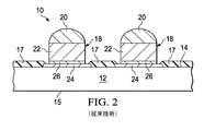
図1により図示されるように、従来のフリップチップダイ10は、内部回路要素を含む半導体基板12を含む。この基板は、第1又はアクティブ面14と、第1の面14とは反対の第2又はイナクティブ面15とを有する。銅ピラーのアレイ16が、ダイ10のアクティブ面表面14から突出する。銅ピラーアレイ16は、第1の面14上で任意の所望の構成で配置され得る、多数の個別の銅ピラー18を含む。
As illustrated by FIG. 1, a conventional flip chip die 10 includes a
図2は、ダイ10の第1の面14から突出する一対の従来の銅ピラー18の典型的な構造を図示する。個別の銅ピラー18の各々は、概して円筒状の銅ポスト部22上に搭載される、概して弾丸又は半円形状のはんだティップ部20を含み得る。各銅ポスト部22は、シリコン基板12の頂部表面において形成されるコンタクトパッド24上に搭載される。コンタクトパッド24は、シリコン基板12内で内部回路要素(図示せず)に接続される。銅ポスト部22は、従来、当業界でよく知られている方式でアンダーバンプ金属層26によるなど、コンタクトパッド24に物理的及び電気的に接続され得る。そのため、各銅ピラー18は、コンタクトパッド24及びアンダーバンプ金属層26を介して半導体基板12内で内部回路要素に電気に接続される。ダイ10の頂部表面14上のパッシベーション層17が各銅ピラー18を囲む。
FIG. 2 illustrates the typical structure of a pair of
図3は、フリップチップダイ10の銅ピラー(CuP)18の幾つかに接続されるように適合される基板30の一部の頂部平面図である。基板30は、印刷回路基板、ICパッケージキャリアボード、インターポーザ、又はその他の種類の電気的接続基板であり得る。基板30は、頂部表面32を有し、複数の概して平行のトレース(本明細書では単に「トレース」と呼ぶこともある)34、36、38、40が、頂部表面32上に、従来の又はその他の方法を用いて提供される。トレース34、36、38、40は、銅又は別の導電性金属で作られ得る。トレースは、銅ピラーのはんだティップとのボンディングを促進するために、錫又は銀などの他の材料で被覆され得る。トレース34、36、38、40は、すべて同じ幅のものであり得る空間44、46、48により隔てられる。トレース34、36、38、40も同じ幅のものであり得る。従来技術のトレース34などのための典型的な幅範囲は15μm〜20μmである。トレース間の空間44、46、48は、40μm〜80μmの典型的な幅範囲を有し得る。トレースの幅の、トレース間の空間の幅に対する比は、典型的に約2.5:4である。関連するCuP18のはんだティップ部20が個別のトレース34、36、38、40に接続される位置は、52、54、56、58において破線の円及び十字線で図示されている。トレース34、36などの対向する長手方向端部は、それぞれ、ソルダレジストのストリップ62、64で覆われる。ソルダレジストは、はんだ又はその他の導電性材料から導電性パッド及びトレースをシールドするために用いられる非導電性の材料である。ソルダレジストは、当業界では「はんだマスク」と呼ぶこともある。トレース端部にわたって提供されるソルダレジストストリップの典型的な幅(トレースが延在する方向に平行な方向)範囲は、約70μm〜170μmである。
FIG. 3 is a top plan view of a portion of a
図4は、図3の基板30のように、フリップチップダイ10の銅ピラー(CuP)18の幾つかに接続されるように適合される基板31の一部の頂部平面図である。基板31の構造は、各トレースの上の小さなソルダレジスト開口を除くトレースをソルダレジストの層が完全に覆うことを除き、基板30のものに類似する。半導体基板31は、その頂部表面33上に形成される、平行の離間されたトレース又は「トレース」35、37、39、41を有する。ソルダレジスト63の層が、ソルダレジスト開口51、53、55、57が提供される、各トレース35、37、39、41の中間部の上方の小さな開口51、53、55、57を除いて、トレースの両端間のトレースの全てを覆う。これらの開口は、各トレースの幅よりいくらか大きく、互い違い(千鳥状)の関係に提供される。開口51、53、55、57はまた、CuP52、54、56、58の直径より幅広く、これらは、開口51、53、55、57により露出される対応するトレースの部分にボンディングされる。
FIG. 4 is a top plan view of a portion of a
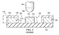
図5は、図4に示す基板31のものと実質的に同じ構造を有する基板110の断面立面図である。基板110は誘電体層112を有する。誘電体層112の頂部表面111上に第1のトレース114が形成される。トレース114は、銅トレースであり得、又は金などの別の適切な導体から形成され得る。図5に示すように、はんだと容易にボンディングし得る導体被覆116、例えば錫又は銀、がトレース114の一部の頂部及び側面を覆う。被覆116が付けられるトレース114の部分は、ソルダレジスト開口132内に配置される。第2のトレース118が、トレース112の1つの側部に隣接して配置され、第3のトレース122が、第1のトレース112の他の側部に近接して配置される。ソルダレジスト層130が、第1のトレース114の中間部115の上に配置されるソルダレジスト開口132など、各トレースの中間部の上方のソルダレジスト開口のエリアを除いて、トレース114、118、122の全てを覆う。ソルダレジスト開口は、図4に示すソルダレジスト開口51、53、55、57のように互い違いである。そのため、図5において、トレース114の上の開口132に隣接する位置の上におけるトレース118及び122の上に開口はない。ソルダレジスト130は、ソルダレジスト開口132にあるトレース114の中間部115に隣接するトレース118及び122の頂部及び側部両方を覆う。開口132におけるソルダレジスト層130の高さ「s1」は、基板表面111から第1のトレース114上の導電性被覆116の頂部まで測定された高さ「t1」より大きい。はんだティップ142を有するCuP140が、トレース114の中間部115の直上に配置され、それを被覆116と接触させるよう下方に移動させることにより、及びその後、はんだティップ142及び被覆116をリフローすることにより、トレース114にボンディングされ得る。CuPのティップの被覆されたトレースへのボンディングは当業界で既知であり、そのため、本明細書に更に記載することはない。
FIG. 5 is a cross-sectional elevation view of a
出願人は、上記で図4及び図5を参照して説明したものなどのフリップチップダイ搭載基板に関連付けられる幾つかの問題を見出している。問題の1つは、このような基板に対する製造上公差が非常に小さく、これらの公差から逸脱すると、幾つかの異なる方式においてフリップチップ/基板アッセンブリが作用しなくなり得るということである。例えば、ソルダレジスト層130が誘電体層112a上で図5に示す位置から左に小さな距離シフトされる場合、トレース118の一部が露出され得、リフローの間ソルダレジスト開口132に入り得るCuP140からの如何なるはんだ142も、トレース114及び118を短絡させ得る。左への同じシフトが、トレース114とトレース122と間の開口132の部分を減少させ得、そのため、トレース122の周りのソルダレジストによりCuP140がトレース114のティップとの接触関係へ自由に動かないようにされ得る。CuP140が下降するにつれて、それは、トレース122の周りのソルダレジストの一部をそぎ落とし得、ソルダレジストのそぎ落とされた部分が被覆層116上に落ち、はんだティップ142と被覆層116との間のボンドと干渉する。ソルダレジスト開口132が小さすぎると、同様の問題が生じ、ソルダレジスト開口132のエリアにおけるトレース122の被覆層116上に落ちるソルダレジスト残留物となる。また、ソルダレジストの開口サイズを小さくすることは、CuPティップ142とトレース114との間の良好なコンタクトを成さないリスクを増大させる。このような問題が生じることを避けるため、ソルダレジスト開口132のサイズは増大され得る。しかし、ソルダレジスト開口132のサイズを増大すると、異なる欠陥モード、いわゆる「ソルダレジストアンダーカット」となり得る。アンダーカットは、118及び122など隣接するCuトレース上を覆うソルダレジストの幅が低減するとき、しばしば起こる。ソルダレジスト開口が大き過ぎず小さ過ぎないようにソルダレジスト開口をつくるプロセスを最適化するには非常にコストがかかる。上述のような問題を予防するために、下記の構造及びプロセスが用いられ得る。
The applicant has found several problems associated with flip chip die mounting substrates such as those described above with reference to FIGS. 4 and 5. One of the problems is that the manufacturing tolerances for such substrates are very small and deviation from these tolerances may cause the flip chip / substrate assembly to fail in several different ways. For example, if the solder resist
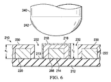
図6は、頂部表面213を備えた誘電体層212を有する半導体基板210の側部立面図である。表面213上に第1のトレース214が形成される。トレース214は、銅、金、又はその他の適切な導体であり得る。第1のトレース214は、ソルダレジスト層230のソルダレジスト開口232内に配置される長さの中間部215を有する。第1の導電性被覆層216が第1のトレース214の中間部215を覆う。この層216は、下記で更に詳細に説明するようにリフロー過熱の間それが融解しない、充分に高い融解温度を有する銅などの導電性材料から形成される。第2の被覆218が、その中間部215における第1のトレース214上の第1の被覆216の上に付けられ得る。被覆層216、218はいずれも導電性被覆層である。第1の被覆層216は、トレース214に類似する組成を有し得る。例えば、トレース及び第1の被覆層216はいずれも銅であり得る。一実施例において第1の被覆層216は、第2の被覆層218より厚い。第1の被覆層216は、トレース214に良好に付着し、リフロー温度で溶融しない材料から選択され得る。第2の被覆層218は、第1の被覆層に良好に付着し、はんだに良好に接着し、リフロー温度で溶融する、導電性材料から選択され得る。例えば、第2の層は、錫又は銀又は適切な合金であり得る。被覆216、218は、従来の手段によるソルダレジスト開口232の形成後、中間部215に付けられ得る。第1のトレース214の1つの側部に平行に及び隣接して第2のトレース220が配置される。第1のトレース214の他方の側部に平行に及び隣接して第3のトレース222が配置される。組み合わされた第2及び第3の層216、218の厚み「t2」は、開口232におけるソルダレジスト層230の高さ「s1」より大きい。そのため、銅ピラー240が下降するにつれて、それは、たとえ銅ピラー240がトレース214上で正確に中央になくても、ソルダレジスト層230ではなく、まずトレース214の第2の層216との接触を成す。これは、第2の層216の頂部が銅ピラー240の付近で基板210上の最も高い表面であるためである。その結果、CuP240のはんだティップ242が、ソルダレジスト層230に接触する如何なる機会をも有する前に第2の層216との接触を成す。従って、図7に図示するように、被覆層218とはんだティップ242と間のボンド250が、図7に図示するように、ソルダレジスト層230からの如何なるデブリもなく形成される。トレース214のコンタクト表面をソルダレジスト層230の上方に上げることにより、別のプラスの効果も達成される。ソルダレジスト開口232は、もはやCuP240がソルダレジスト開口にフィットする必要がないため、CuP240のサイズに対してサイズが低減され得る。そのため、ソルダレジストアンダーカットが避けられる。またCuPの240の直径は、ソルダレジスト開口のサイズに対して増大され得る。CuPの直径を増大させると、各CuPが対応するトレースとより容易に係合され得る。言い換えると、他の問題を生じさせることなく各CuPに一層広いフットプリントが与えられ得るため、CuPと対応するトレースとの間の整合は、図6及び図7に示す構造では図3〜図5に示す構造の場合ほど正確である必要はない。例えば、図6及び図7に示すように、CuPは、210などの基板に機能的に接続可能である対応するソルダレジスト開口232より幅広いフットプリントでつくられ得、この基板は、ソルダレジスト層230の高さs1より大きい対応するソルダレジスト開口232における全体的なトレース高さt2(被覆を含む)を有する。CuPには、たとえその断面形状が、例えば楕円又は矩形又はその他の幾何学形状など、円以外であっても、一層広いフットプリントが与えられ得ることも理解されたい。そのため、欠陥アッセンブリが低減され得、また、図6及び図7において図示及び説明されるような構造により製品歩留まり率が改善され得る。
FIG. 6 is a side elevational view of a
図8は、フリップチップダイ、及び図6及び図7に図示するものと同じであり得る断面構成を有する基板アッセンブリタイプの頂部平面図である。この実施例において、トレース214、220、222などは、各々第1端部262及び第2端部264を有する。例えば214、220など、隣接するトレースの第1端部262と第2端部264とは互い違いにされる。その結果、例えば、220、222など、1つおきのトレースの第1端部262は同じ想像線AAで終端し、他のトレース214などの第1端部264は線AAの実質的に内側に配置される。トレースの第2端部264及び想像線BBに対して同じ関係がある。ソルダレジスト層230の端部は、線AA及びBBに沿っていてもよく、又はそれらの外にあってもよい。平行のトレースの任意のアレイにおける如何なるトレースも全て、同じ想像線で開始し、同じ想像線での端部で終わるという、トレースの従来技術の位置決めに対するこの位置決めの利点は、図8の基板210上のトレースの総長が実質的に低減される点である。また、隣接するトレースの内側に位置する端部262又は264が、図8に示すように、隣接するトレース間に重なりがないように終端する場合、隣接するトレース間の短絡の可能性が実質的に低減される。(本明細書において用いられるように語句「隣接するトレース」とは、たとえトレース自体が部分的に同一広がりを有さない(coextensive)長さであるときでも、隣接する軸を有するトレースを指す。)その結果、トレース間の横方向距離が低減され得、一層密度の高い設計が可能となり、そのため、一層高ピッチの関連するCuPフリップチップダイの利用が可能となる。またトレース長さがより短いことで、Cuマイグレーションの可能性、及び、寄生容量などの何らかの望ましくない電気的影響の可能性が低減され得る。また、一層大きなソルダレジスト開口の利用も可能となり、そのため、従来技術のものより一層容易に製造し得る基板設計の利用が可能となる。
FIG. 8 is a top plan view of a flip chip die and a substrate assembly type having a cross sectional configuration that may be the same as illustrated in FIGS. 6 and 7. In this example, the
図9は、銅ピラー取り付け基板を形成する方法のブロック図である。この方法は、302で図示するように、誘電体層を備えた基板を提供することを含む。この方法はまた、304で図示するように、誘電体層上に複数の平行のトレースを形成することを含む。この方法は更に、306で図示するように、複数の平行のトレースの上にソルダレジスト層を付けることを含み、また、308で図示するように、ソルダレジスト層に各トレースの中間部分を露出させる開口を形成することを含む。この方法は更に、310で図示するように、トレースの各々の露出された中間部を、ソルダレジスト層の高さより高い高さまで延在する導電性材料で被覆することを含む。 FIG. 9 is a block diagram of a method of forming a copper pillar attached substrate. The method includes providing a substrate with a dielectric layer, as illustrated at 302. The method also includes forming a plurality of parallel traces on the dielectric layer, as illustrated at 304. The method further includes applying a solder resist layer over the plurality of parallel traces, as illustrated at 306, and exposing an intermediate portion of each trace to the solder resist layer, as illustrated at 308. Including forming an opening. The method further includes coating the exposed middle portion of each of the traces with a conductive material extending to a height higher than the height of the solder resist layer, as illustrated at 310.
当業者であれば、本発明の特許請求の範囲内で、説明した例示の実施例に変形が成され得ること、及び多くの他の実施例が可能であることが分かるであろう。 Those skilled in the art will appreciate that modifications may be made to the illustrated embodiments described within the scope of the claims of the present invention, and that many other embodiments are possible.
Claims (17)
銅ピラー取り付け基板であって、
誘電体層と、
前記誘電体層に重なるソルダレジスト層であって、その中に複数の開口を有し、且つ、ソルダレジスト層高さを有する、前記ソルダレジスト層と、
前記誘電体層上に形成される複数の平行のトレースであって、各トレースが第1の端部と第2の端部と前記第1及び第2の端部の間の中間部とを有し、前記第1及び第2の端部が前記ソルダレジスト層により覆われ、前記中間部が前記ソルダレジスト層の前記開口内に配置され、前記中間部の各々が、その上に少なくとも1つの導電性被覆層を有し、前記ソルダレジスト層高さより大きい、前記誘電体層から前記少なくとも1つの導電性被覆層の最頂のものまでの測定された高さを有する、前記複数の平行のトレースと、
を含む、前記銅ピラー取り付け基板と、
前記少なくとも1つの導電性被覆層に取り付けられるはんだと、
を含む、アッセンブリ。 Electronic assembly,
A copper pillar mounting substrate,
Dielectric layer,
A solder resist layer overlapping the dielectric layer, the solder resist layer having a plurality of openings therein and having a solder resist layer height ;
A plurality of parallel traces formed on the dielectric layer, each trace having a first end, a second end, and an intermediate portion between the first and second ends. Said first and second ends are covered by said solder resist layer, said middle part is arranged in said opening of said solder resist layer, each of said middle parts being at least one electrically conductive thereon A plurality of parallel traces having a conductive covering layer and having a measured height greater than the solder resist layer height , from the dielectric layer to the top of the at least one conductive covering layer; ,
And said copper pillar mounting substrate,
Solder attached to the at least one conductive coating layer;
Including the assembly.
前記少なくとも1つの導電性被覆層が第1の導電性被覆層と第2の導電性被覆層とを含む、アッセンブリ。 An assembly according to claim 1, wherein
An assembly, wherein the at least one conductive coating layer comprises a first conductive coating layer and a second conductive coating layer.
前記第1の導電性被覆層が銅を含む、アッセンブリ。 The assembly according to claim 2, wherein
An assembly, wherein the first conductive coating layer comprises copper.
前記第2の導電性被覆層が錫を含む、アッセンブリ。 The assembly according to claim 2, wherein
The assembly wherein the second conductive coating layer comprises tin.
前記トレースが銅を含む、アッセンブリ。 An assembly according to claim 1, wherein
An assembly, wherein the traces comprise copper.
前記ソルダレジスト層における前記開口が互い違いにされる、アッセンブリ。 An assembly according to claim 1, wherein
The assembly wherein the openings in the solder resist layer are staggered.
複数の銅ピラーを有するダイを更に含み、
前記銅ピラーの各々が、前記複数のトレースの関連する1つのトレースの前記中間部に接続される前記はんだとしてのはんだティップ部を有し、前記銅ピラーの各々が、前記平行のトレースに垂直に測定された前記ソルダレジスト開口の関連する1つのソルダレジスト開口の寸法より大きい、前記平行のトレースに垂直に測定された断面寸法を有し、
前記複数の平行のトレースの隣接するトレースがトレース間隔距離により隔てられ、前記ソルダレジスト層開口が互い違いにされる、アッセンブリ。 An assembly according to claim 1, wherein
Further comprising a die having a plurality of copper pillars,
Each of the copper pillars has a solder tip as the solder connected to the middle of the associated one of the plurality of traces, each of the copper pillars being perpendicular to the parallel traces Having a cross-sectional dimension measured perpendicular to the parallel traces, which is greater than the dimension of the associated solder resist aperture of the solder resist aperture measured;
An assembly, wherein adjacent traces of the plurality of parallel traces are separated by a trace spacing distance, and the solder resist layer openings are staggered.
前記銅ピラーの各々の前記はんだティップ部が、前記複数のトレースの関連する1つのトレースの前記中間部上の前記少なくとも1つの導電性被覆層にボンディングされる、アッセンブリ。 The assembly according to claim 7, wherein
An assembly, wherein the solder tip portion of each of the copper pillars is bonded to the at least one conductive covering layer on the middle portion of an associated one of the plurality of traces.
前記複数のトレースの各々の前記中間部上の前記少なくとも1つの導電性被覆層が、第1の被覆層と、前記第1の被覆層の上の第2の被覆層とを含み、前記銅ピラーの前記はんだティップ部が前記第2の被覆層にボンディングされる、アッセンブリ。 The assembly according to claim 8, wherein
The at least one conductive coating layer on the middle portion of each of the plurality of traces includes a first coating layer and a second coating layer on the first coating layer, the copper pillar An assembly wherein the solder tip portion of is bonded to the second cover layer.
前記第1の被覆層が前記第2の被覆層より厚い、アッセンブリ。 The assembly according to claim 9, wherein
An assembly, wherein the first covering layer is thicker than the second covering layer.
前記はんだティップ部の各々が円形の断面を有する、アッセンブリ。 The assembly according to claim 7, wherein
An assembly, wherein each of said solder tips has a circular cross section.
前記複数の平行のトレースが、前記トレースに垂直であり且つ前記第1の端部のうちの最外の第1の端部に交差する第1の線と、前記トレースに垂直であり且つ前記第2の端部のうちの最外の第2の端部に交差する第2の線とにより画定されるエリア内に配置され、前記複数のトレースが各々前記第1の線と前記第2の線との間の距離より短い長さを有する、アッセンブリ。 An assembly according to claim 1, wherein
A first line perpendicular to the trace and intersecting the outermost first end of the first ends, and a plurality of parallel traces perpendicular to the trace and the first line; The plurality of traces being disposed in an area defined by a second line intersecting the outermost second end of the two ends, the plurality of traces each being the first line and the second line An assembly having a length less than the distance between and.
前記複数のトレースが各々前記第1の線と前記第2の線との間の前記距離の2分の1より短い長さを有する、アッセンブリ。 The assembly according to claim 12, wherein
An assembly, wherein the plurality of traces each have a length less than half of the distance between the first line and the second line.
前記ソルダレジスト層が、少なくとも、前記第1の線まで、及び前記複数の平行のトレースの少なくとも最初のトレースから前記複数の平行のトレースの少なくとも最後のトレースまで延在する領域において前記第2の線まで延在する、アッセンブリ。 The assembly according to claim 12, wherein
The second line in a region where the solder resist layer extends at least to the first line and from at least a first trace of the plurality of parallel traces to at least a last trace of the plurality of parallel traces. Extending to the assembly.
誘電体層を備えた基板を提供することと、
前記誘電体層上に複数の平行のトレースを形成することと、
前記複数の平行のトレースの上にソルダレジスト層を付けることと、
各トレースの中間部分を露出させる前記ソルダレジスト層における開口を形成することと、
前記トレースの各々の前記露出された中間部を、前記ソルダレジスト層の高さより高い高さまで延在する導電性材料で被覆することと、
前記導電性材料上にはんだを取り付けることと、
を含む、方法。 A method of forming a copper pillar mounting substrate, comprising:
Providing a substrate with a dielectric layer;
Forming a plurality of parallel traces on the dielectric layer;
Applying a solder resist layer over the plurality of parallel traces;
Forming an opening in the solder resist layer exposing the middle portion of each trace;
Covering the exposed middle portion of each of the traces with a conductive material extending to a height higher than the height of the solder resist layer;
Attaching a solder on the conductive material;
Method, including.
前記誘電体層上に前記複数の平行のトレースを形成することが、隣接するトレースの長さが重ならないように、平行のトレースの開始点と終点とを互い違いにすることを含む、方法。 The method according to claim 15 , wherein
Forming the plurality of parallel traces on the dielectric layer comprises staggering the start and end points of the parallel traces such that the lengths of adjacent traces do not overlap.
各トレースの中間部分を露出させる前記ソルダレジスト層において前記開口を形成することが、互い違いの開口を形成することを含む、方法。 The method according to claim 15 , wherein
Forming the openings in the solder resist layer exposing the middle portion of each trace includes forming staggered openings.
Applications Claiming Priority (3)
| Application Number | Priority Date | Filing Date | Title |
|---|---|---|---|
| US13/798,678 | 2013-03-13 | ||
| US13/798,678 US8896118B2 (en) | 2013-03-13 | 2013-03-13 | Electronic assembly with copper pillar attach substrate |
| PCT/US2014/022334 WO2014164402A1 (en) | 2013-03-13 | 2014-03-10 | Copper pillar attach substrate |
Publications (3)
| Publication Number | Publication Date |
|---|---|
| JP2016519420A JP2016519420A (en) | 2016-06-30 |
| JP2016519420A5 JP2016519420A5 (en) | 2017-04-13 |
| JP6503334B2 true JP6503334B2 (en) | 2019-04-17 |
Family
ID=51523877
Family Applications (1)
| Application Number | Title | Priority Date | Filing Date |
|---|---|---|---|
| JP2016500941A Active JP6503334B2 (en) | 2013-03-13 | 2014-03-10 | Copper pillar mounting board |
Country Status (4)
| Country | Link |
|---|---|
| US (1) | US8896118B2 (en) |
| JP (1) | JP6503334B2 (en) |
| CN (1) | CN105190879B (en) |
| WO (1) | WO2014164402A1 (en) |
Families Citing this family (3)
| Publication number | Priority date | Publication date | Assignee | Title |
|---|---|---|---|---|
| DE112016007096B4 (en) * | 2016-07-28 | 2023-06-29 | Mitsubishi Electric Corporation | semiconductor device |
| JP6691031B2 (en) * | 2016-10-05 | 2020-04-28 | 新光電気工業株式会社 | Wiring board, manufacturing method thereof, and semiconductor package |
| CN109729639B (en) * | 2018-12-24 | 2020-11-20 | 奥特斯科技(重庆)有限公司 | Component carrier comprising columns on coreless substrate |
Family Cites Families (13)
| Publication number | Priority date | Publication date | Assignee | Title |
|---|---|---|---|---|
| JPH11191672A (en) * | 1997-12-25 | 1999-07-13 | Victor Co Of Japan Ltd | Printed wiring board |
| JP3891838B2 (en) * | 2001-12-26 | 2007-03-14 | 株式会社ルネサステクノロジ | Semiconductor device and manufacturing method thereof |
| JP3829325B2 (en) * | 2002-02-07 | 2006-10-04 | 日本電気株式会社 | Semiconductor element, manufacturing method thereof, and manufacturing method of semiconductor device |
| KR100722645B1 (en) * | 2006-01-23 | 2007-05-28 | 삼성전기주식회사 | Method for manufacturing printed circuit board for semi-conductor package and printed circuit board manufactured therefrom |
| JP2008098402A (en) * | 2006-10-12 | 2008-04-24 | Renesas Technology Corp | Semiconductor device and its manufacturing method |
| KR20090080623A (en) * | 2008-01-22 | 2009-07-27 | 삼성전기주식회사 | Post bump and forming method of the same |
| JP5088489B2 (en) * | 2008-03-03 | 2012-12-05 | セイコーエプソン株式会社 | Semiconductor module and manufacturing method thereof |
| US7851345B2 (en) * | 2008-03-19 | 2010-12-14 | Stats Chippac, Ltd. | Semiconductor device and method of forming oxide layer on signal traces for electrical isolation in fine pitch bonding |
| JP5707316B2 (en) * | 2009-03-12 | 2015-04-30 | ナミックス株式会社 | Electronic component mounting method |
| GB2487338B (en) | 2009-12-23 | 2014-10-22 | Skyworks Solutions Inc | Surface mount spark gap |
| US8587119B2 (en) * | 2010-04-16 | 2013-11-19 | Taiwan Semiconductor Manufacturing Company, Ltd. | Conductive feature for semiconductor substrate and method of manufacture |
| US8367467B2 (en) | 2010-04-21 | 2013-02-05 | Stats Chippac, Ltd. | Semiconductor method of forming bump on substrate to prevent ELK ILD delamination during reflow process |
| US9905524B2 (en) * | 2011-07-29 | 2018-02-27 | Taiwan Semiconductor Manufacturing Company, Ltd. | Bump structures in semiconductor device and packaging assembly |
-
2013
- 2013-03-13 US US13/798,678 patent/US8896118B2/en active Active
-
2014
- 2014-03-10 CN CN201480014113.5A patent/CN105190879B/en active Active
- 2014-03-10 WO PCT/US2014/022334 patent/WO2014164402A1/en active Application Filing
- 2014-03-10 JP JP2016500941A patent/JP6503334B2/en active Active
Also Published As
| Publication number | Publication date |
|---|---|
| WO2014164402A1 (en) | 2014-10-09 |
| CN105190879A (en) | 2015-12-23 |
| US8896118B2 (en) | 2014-11-25 |
| JP2016519420A (en) | 2016-06-30 |
| US20140264829A1 (en) | 2014-09-18 |
| CN105190879B (en) | 2018-07-03 |
Similar Documents
| Publication | Publication Date | Title |
|---|---|---|
| KR101478875B1 (en) | Package on package devices and methods of packaging semiconductor dies | |
| US11101238B2 (en) | Surface mounting semiconductor components | |
| US9502390B2 (en) | BVA interposer | |
| KR101548428B1 (en) | Package having substrate with embedded metal trace overlapped by landing pad | |
| US10600709B2 (en) | Bump-on-trace packaging structure and method for forming the same | |
| JP2017022408A (en) | Microelectronic package with dual or multiple-etched flip-chip connector and corresponding manufacturing method | |
| US9111818B2 (en) | Packaging substrate | |
| TWI591785B (en) | Semiconductor device and method of manufacturing the same | |
| US8659168B2 (en) | Wiring board for flip-chip mounting, mounting structure of electronic components on wiring board, and semiconductor device including wiring board | |
| TW201911508A (en) | Electronic package | |
| US7074704B2 (en) | Bump formed on semiconductor device chip and method for manufacturing the bump | |
| US20150380345A1 (en) | Semiconductor device | |
| KR100967565B1 (en) | Semiconductor component | |
| US9219052B2 (en) | Making a flip-chip assembly with bond fingers | |
| JP6503334B2 (en) | Copper pillar mounting board | |
| US9524944B2 (en) | Method for fabricating package structure | |
| US9559076B2 (en) | Package having substrate with embedded metal trace overlapped by landing pad | |
| TWI666746B (en) | Flip-chip package substrate, flip-chip package and manufacturing method thereof | |
| TWI641090B (en) | Electronic package | |
| US8828799B2 (en) | Method of forming an integrated circuit package including a direct connect pad, a blind via, and a bond pad electrically coupled to the direct connect pad | |
| US20070267730A1 (en) | Wafer level semiconductor chip packages and methods of making the same |
Legal Events
| Date | Code | Title | Description |
|---|---|---|---|
| A521 | Request for written amendment filed |
Free format text: JAPANESE INTERMEDIATE CODE: A523 Effective date: 20170307 |
|
| A621 | Written request for application examination |
Free format text: JAPANESE INTERMEDIATE CODE: A621 Effective date: 20170307 |
|
| A131 | Notification of reasons for refusal |
Free format text: JAPANESE INTERMEDIATE CODE: A131 Effective date: 20180523 |
|
| A521 | Request for written amendment filed |
Free format text: JAPANESE INTERMEDIATE CODE: A523 Effective date: 20180810 |
|
| A131 | Notification of reasons for refusal |
Free format text: JAPANESE INTERMEDIATE CODE: A131 Effective date: 20181107 |
|
| A521 | Request for written amendment filed |
Free format text: JAPANESE INTERMEDIATE CODE: A523 Effective date: 20190207 |
|
| TRDD | Decision of grant or rejection written | ||
| A01 | Written decision to grant a patent or to grant a registration (utility model) |
Free format text: JAPANESE INTERMEDIATE CODE: A01 Effective date: 20190306 |
|
| A61 | First payment of annual fees (during grant procedure) |
Free format text: JAPANESE INTERMEDIATE CODE: A61 Effective date: 20190325 |
|
| R150 | Certificate of patent or registration of utility model |
Ref document number: 6503334 Country of ref document: JP Free format text: JAPANESE INTERMEDIATE CODE: R150 |
|
| S111 | Request for change of ownership or part of ownership |
Free format text: JAPANESE INTERMEDIATE CODE: R313117 |
|
| R360 | Written notification for declining of transfer of rights |
Free format text: JAPANESE INTERMEDIATE CODE: R360 |
|
| R350 | Written notification of registration of transfer |
Free format text: JAPANESE INTERMEDIATE CODE: R350 |
|
| R250 | Receipt of annual fees |
Free format text: JAPANESE INTERMEDIATE CODE: R250 |
|
| R250 | Receipt of annual fees |
Free format text: JAPANESE INTERMEDIATE CODE: R250 |
|
| R250 | Receipt of annual fees |
Free format text: JAPANESE INTERMEDIATE CODE: R250 |