JP6501581B2 - Light source device, image display device, and control method of light source device - Google Patents
Light source device, image display device, and control method of light source device Download PDFInfo
- Publication number
- JP6501581B2 JP6501581B2 JP2015064872A JP2015064872A JP6501581B2 JP 6501581 B2 JP6501581 B2 JP 6501581B2 JP 2015064872 A JP2015064872 A JP 2015064872A JP 2015064872 A JP2015064872 A JP 2015064872A JP 6501581 B2 JP6501581 B2 JP 6501581B2
- Authority
- JP
- Japan
- Prior art keywords
- led
- light emitting
- light
- mode
- drive mode
- Prior art date
- Legal status (The legal status is an assumption and is not a legal conclusion. Google has not performed a legal analysis and makes no representation as to the accuracy of the status listed.)
- Expired - Fee Related
Links
- 238000000034 method Methods 0.000 title claims description 46
- 239000003086 colorant Substances 0.000 claims description 10
- 239000004065 semiconductor Substances 0.000 claims description 5
- JMASRVWKEDWRBT-UHFFFAOYSA-N Gallium nitride Chemical compound [Ga]#N JMASRVWKEDWRBT-UHFFFAOYSA-N 0.000 claims description 4
- 229910002601 GaN Inorganic materials 0.000 claims description 3
- 235000019557 luminance Nutrition 0.000 description 78
- 239000000758 substrate Substances 0.000 description 49
- 230000008859 change Effects 0.000 description 34
- 230000007423 decrease Effects 0.000 description 29
- 230000008569 process Effects 0.000 description 22
- 230000032683 aging Effects 0.000 description 17
- 239000004973 liquid crystal related substance Substances 0.000 description 14
- 238000001514 detection method Methods 0.000 description 8
- 230000006870 function Effects 0.000 description 8
- 230000003287 optical effect Effects 0.000 description 8
- 230000006866 deterioration Effects 0.000 description 6
- 238000009792 diffusion process Methods 0.000 description 6
- 230000009467 reduction Effects 0.000 description 6
- 238000010586 diagram Methods 0.000 description 5
- 230000006872 improvement Effects 0.000 description 5
- 238000006243 chemical reaction Methods 0.000 description 3
- 230000003247 decreasing effect Effects 0.000 description 3
- 230000001133 acceleration Effects 0.000 description 2
- 230000015556 catabolic process Effects 0.000 description 2
- 230000004313 glare Effects 0.000 description 2
- 238000001228 spectrum Methods 0.000 description 2
- GYHNNYVSQQEPJS-UHFFFAOYSA-N Gallium Chemical compound [Ga] GYHNNYVSQQEPJS-UHFFFAOYSA-N 0.000 description 1
- PEDCQBHIVMGVHV-UHFFFAOYSA-N Glycerine Chemical compound OCC(O)CO PEDCQBHIVMGVHV-UHFFFAOYSA-N 0.000 description 1
- URRHWTYOQNLUKY-UHFFFAOYSA-N [AlH3].[P] Chemical compound [AlH3].[P] URRHWTYOQNLUKY-UHFFFAOYSA-N 0.000 description 1
- 230000007613 environmental effect Effects 0.000 description 1
- 229910052733 gallium Inorganic materials 0.000 description 1
- 229910052738 indium Inorganic materials 0.000 description 1
- APFVFJFRJDLVQX-UHFFFAOYSA-N indium atom Chemical compound [In] APFVFJFRJDLVQX-UHFFFAOYSA-N 0.000 description 1
- 238000009607 mammography Methods 0.000 description 1
- 238000004519 manufacturing process Methods 0.000 description 1
- 239000011159 matrix material Substances 0.000 description 1
- 230000002093 peripheral effect Effects 0.000 description 1
- 238000011946 reduction process Methods 0.000 description 1
- 230000004044 response Effects 0.000 description 1
- 238000003860 storage Methods 0.000 description 1
- 238000002834 transmittance Methods 0.000 description 1
Images


Classifications
-
- G—PHYSICS
- G09—EDUCATION; CRYPTOGRAPHY; DISPLAY; ADVERTISING; SEALS
- G09G—ARRANGEMENTS OR CIRCUITS FOR CONTROL OF INDICATING DEVICES USING STATIC MEANS TO PRESENT VARIABLE INFORMATION
- G09G3/00—Control arrangements or circuits, of interest only in connection with visual indicators other than cathode-ray tubes
- G09G3/20—Control arrangements or circuits, of interest only in connection with visual indicators other than cathode-ray tubes for presentation of an assembly of a number of characters, e.g. a page, by composing the assembly by combination of individual elements arranged in a matrix no fixed position being assigned to or needed to be assigned to the individual characters or partial characters
- G09G3/34—Control arrangements or circuits, of interest only in connection with visual indicators other than cathode-ray tubes for presentation of an assembly of a number of characters, e.g. a page, by composing the assembly by combination of individual elements arranged in a matrix no fixed position being assigned to or needed to be assigned to the individual characters or partial characters by control of light from an independent source
- G09G3/3406—Control of illumination source
- G09G3/3413—Details of control of colour illumination sources
-
- G—PHYSICS
- G09—EDUCATION; CRYPTOGRAPHY; DISPLAY; ADVERTISING; SEALS
- G09G—ARRANGEMENTS OR CIRCUITS FOR CONTROL OF INDICATING DEVICES USING STATIC MEANS TO PRESENT VARIABLE INFORMATION
- G09G3/00—Control arrangements or circuits, of interest only in connection with visual indicators other than cathode-ray tubes
- G09G3/20—Control arrangements or circuits, of interest only in connection with visual indicators other than cathode-ray tubes for presentation of an assembly of a number of characters, e.g. a page, by composing the assembly by combination of individual elements arranged in a matrix no fixed position being assigned to or needed to be assigned to the individual characters or partial characters
- G09G3/2007—Display of intermediate tones
- G09G3/2077—Display of intermediate tones by a combination of two or more gradation control methods
- G09G3/2081—Display of intermediate tones by a combination of two or more gradation control methods with combination of amplitude modulation and time modulation
-
- G—PHYSICS
- G09—EDUCATION; CRYPTOGRAPHY; DISPLAY; ADVERTISING; SEALS
- G09G—ARRANGEMENTS OR CIRCUITS FOR CONTROL OF INDICATING DEVICES USING STATIC MEANS TO PRESENT VARIABLE INFORMATION
- G09G3/00—Control arrangements or circuits, of interest only in connection with visual indicators other than cathode-ray tubes
- G09G3/20—Control arrangements or circuits, of interest only in connection with visual indicators other than cathode-ray tubes for presentation of an assembly of a number of characters, e.g. a page, by composing the assembly by combination of individual elements arranged in a matrix no fixed position being assigned to or needed to be assigned to the individual characters or partial characters
- G09G3/34—Control arrangements or circuits, of interest only in connection with visual indicators other than cathode-ray tubes for presentation of an assembly of a number of characters, e.g. a page, by composing the assembly by combination of individual elements arranged in a matrix no fixed position being assigned to or needed to be assigned to the individual characters or partial characters by control of light from an independent source
- G09G3/3406—Control of illumination source
- G09G3/342—Control of illumination source using several illumination sources separately controlled corresponding to different display panel areas, e.g. along one dimension such as lines
- G09G3/3426—Control of illumination source using several illumination sources separately controlled corresponding to different display panel areas, e.g. along one dimension such as lines the different display panel areas being distributed in two dimensions, e.g. matrix
-
- G—PHYSICS
- G09—EDUCATION; CRYPTOGRAPHY; DISPLAY; ADVERTISING; SEALS
- G09G—ARRANGEMENTS OR CIRCUITS FOR CONTROL OF INDICATING DEVICES USING STATIC MEANS TO PRESENT VARIABLE INFORMATION
- G09G2320/00—Control of display operating conditions
- G09G2320/06—Adjustment of display parameters
- G09G2320/0626—Adjustment of display parameters for control of overall brightness
- G09G2320/064—Adjustment of display parameters for control of overall brightness by time modulation of the brightness of the illumination source
-
- G—PHYSICS
- G09—EDUCATION; CRYPTOGRAPHY; DISPLAY; ADVERTISING; SEALS
- G09G—ARRANGEMENTS OR CIRCUITS FOR CONTROL OF INDICATING DEVICES USING STATIC MEANS TO PRESENT VARIABLE INFORMATION
- G09G2320/00—Control of display operating conditions
- G09G2320/06—Adjustment of display parameters
- G09G2320/066—Adjustment of display parameters for control of contrast
-
- G—PHYSICS
- G09—EDUCATION; CRYPTOGRAPHY; DISPLAY; ADVERTISING; SEALS
- G09G—ARRANGEMENTS OR CIRCUITS FOR CONTROL OF INDICATING DEVICES USING STATIC MEANS TO PRESENT VARIABLE INFORMATION
- G09G2320/00—Control of display operating conditions
- G09G2320/06—Adjustment of display parameters
- G09G2320/0666—Adjustment of display parameters for control of colour parameters, e.g. colour temperature
-
- G—PHYSICS
- G09—EDUCATION; CRYPTOGRAPHY; DISPLAY; ADVERTISING; SEALS
- G09G—ARRANGEMENTS OR CIRCUITS FOR CONTROL OF INDICATING DEVICES USING STATIC MEANS TO PRESENT VARIABLE INFORMATION
- G09G2330/00—Aspects of power supply; Aspects of display protection and defect management
- G09G2330/02—Details of power systems and of start or stop of display operation
- G09G2330/021—Power management, e.g. power saving
Description
本発明は、光源装置、画像表示装置、及び、光源装置の制御方法に関する。 The present invention relates to a light source device, an image display device, and a control method of the light source device.
カラーフィルタを有するカラー液晶パネルと、カラー液晶パネルの背面に白色光を照射する光源装置(バックライト装置)と、を有するカラー画像表示装置がある。従来、光源装置の光源として、冷陰極管(CCFL:Cold Cathode Fluorescent Lamp)等の蛍光ランプが主に用いられていた。しかし近年、光源装置の光源として、消費電力、寿命、色再現性、環境負荷の面で優れた発光ダイオード(LED:Light Emitting Diode)が用いられるようになってきている。 There is a color image display device having a color liquid crystal panel having a color filter, and a light source device (backlight device) which emits white light on the back surface of the color liquid crystal panel. Heretofore, fluorescent lamps such as cold cathode fluorescent lamps (CCFLs) have been mainly used as light sources of light source devices. However, in recent years, a light emitting diode (LED: Light Emitting Diode) excellent in terms of power consumption, life, color reproducibility and environmental load has come to be used as a light source of a light source device.
光源としてLEDを用いた光源装置(LEDバックライト装置)は、一般に、多数のLEDを有する。特許文献1は、複数の発光ブロックを有するLEDバックライト装置が開示されている。各発光ブロックは、1つ以上のLEDを有する。また、特許文献1には、複数の発光ブロックのそれぞれの発光輝度を個別に制御することが開示されている。 A light source device (LED backlight device) using an LED as a light source generally has a large number of LEDs. Patent Document 1 discloses an LED backlight device having a plurality of light emitting blocks. Each light emitting block comprises one or more LEDs. Further, Patent Document 1 discloses individually controlling the light emission luminance of each of a plurality of light emission blocks.
カラー画像表示装置の画面の低輝度表示領域に光を照射する発光ブロックの発光輝度を低減することで、消費電力を低減でき、表示画像(画面に表示された画像)のコントラストを向上できる。低輝度表示領域は、暗い画像が表示される領域である。また、画面の高輝度表示領域に光を照射する発光ブロックの発光輝度を高めることで、表示画像のコントラストを向上でき、従来表現できなかった眩しさや煌めきを表現できる。高輝度表示領域は、明るい画像が表示される領域である。そして、低輝度表示領域に光を照射する発光ブロックの発光輝度を低減し、高輝度表示領域に光を照射する発光ブロックの発光輝度を高めることで、表示画像のコントラストをより向上できる。このような、画像の特徴に応じた各発光ブロックの発光制御は「ローカルディミング制御」と呼ばれる。また、高輝度表示領域に光を照射する発光ブロックの発光輝度を高めるローカルディミング制御は「HDR(High Dynamic Range)制御」と呼ばれる。 By reducing the light emission luminance of the light emission block that emits light to the low luminance display area of the screen of the color image display device, power consumption can be reduced and the contrast of the display image (image displayed on the screen) can be improved. The low luminance display area is an area where a dark image is displayed. In addition, by increasing the light emission luminance of the light emission block that irradiates light to the high luminance display area of the screen, the contrast of the display image can be improved, and it is possible to express glare and glare that could not be expressed conventionally. The high brightness display area is an area where a bright image is displayed. The contrast of the display image can be further improved by reducing the light emission luminance of the light emission block that irradiates light to the low luminance display region and increasing the light emission luminance of the light emission block that irradiates light to the high luminance display region. Such light emission control of each light emission block according to the feature of the image is called "local dimming control". In addition, local dimming control that raises the light emission luminance of a light emission block that emits light to a high luminance display area is called “HDR (High Dynamic Range) control”.
一般的に、装置の消費電力は小さいことが好ましい。上述したように、消費電力を低減可能なローカルディミング制御がある。しかしながら、光源装置がそのようなローカルディミング制御を実行できるとは限らない。また、ユーザがローカルディミング制御を好むとも限らない。そのため、ローカルディミング制御を行わなくても消費電力を低減できる新たな方法が望まれる。 In general, the power consumption of the device is preferably small. As described above, there is local dimming control that can reduce power consumption. However, the light source device can not necessarily perform such local dimming control. Also, the user does not necessarily prefer local dimming control. Therefore, a new method capable of reducing power consumption without performing local dimming control is desired.
本発明は、ローカルディミング制御を行わずに光源装置の消費電力を低減できる技術を提供することを目的とする。 An object of the present invention is to provide a technology capable of reducing the power consumption of a light source device without performing local dimming control.
本発明の第1の態様は、
発光色が互いに異なる複数の発光ダイオードを有する発光手段と、
前記発光手段の駆動方法が互いに異なる第1駆動モードと第2駆動モードを含む複数の駆動モードのいずれかを設定する設定手段と、
前記設定手段によって設定された駆動モードに応じた駆動方法で、前記複数の発光ダイオードのそれぞれが周期的に発光するように、前記発光手段を駆動する制御手段と、
を有し、
前記発光手段を所定の発光輝度で点灯させる場合に、
前記複数の発光ダイオードのうちの一部の発光ダイオードについて、前記第2駆動モードでは、前記第1駆動モードに比べて、点灯期間の駆動電流値が低く、かつ1周期における点灯時間が長い
ことを特徴とする光源装置である。
The first aspect of the present invention is
Light emitting means having a plurality of light emitting diodes different in light emission color from each other;
Setting means for setting any one of a plurality of drive modes including a first drive mode and a second drive mode which are different in drive method of the light emitting means;
Control means for driving the light emitting means such that each of the plurality of light emitting diodes periodically emits light by a driving method according to the driving mode set by the setting means;
Have
When the light emitting means is turned on at a predetermined light emission luminance,
Regarding the light emitting diodes of some of the plurality of light emitting diodes, in the second drive mode, the drive current value in the lighting period is lower than in the first drive mode, and the lighting time in one cycle is longer It is a light source device characterized by
本発明の第2の態様は、
前記光源装置と、
前記光源装置から発せられた光を入力画像データに基づいて変調することにより、画面に画像を表示する表示手段と、
を有することを特徴とする画像表示装置である。
The second aspect of the present invention is
The light source device;
Display means for displaying an image on a screen by modulating light emitted from the light source device based on input image data;
An image display apparatus characterized in that
本発明の第3の態様は、
発光色が互いに異なる複数の発光ダイオードを有する発光手段を有する光源装置の制御方法であって、
前記発光手段の駆動方法が互いに異なる第1駆動モードと第2駆動モードを含む複数の駆動モードのいずれかを設定する設定ステップと、
前記設定ステップによって設定された駆動モードに応じた駆動方法で、前記複数の発光
ダイオードのそれぞれが周期的に発光するように、前記発光手段を駆動する制御ステップと、
を有し、
前記発光手段を所定の発光輝度で点灯させる場合に、
前記複数の発光ダイオードのうちの一部の発光ダイオードについて、前記第2駆動モードでは、前記第1駆動モードに比べて、点灯期間の駆動電流値が低く、かつ1周期における点灯期間が長い
ことを特徴とする光源装置の制御方法である。
The third aspect of the present invention is
A control method of a light source device having light emitting means having a plurality of light emitting diodes having different light emission colors, the light source device comprising:
A setting step of setting one of a plurality of drive modes including a first drive mode and a second drive mode which are different in drive method of the light emitting means;
The plurality of light emissions are driven by a driving method according to the driving mode set in the setting step.
Controlling the light emitting means such that each of the diodes emits light periodically ;
Have
When the light emitting means is turned on at a predetermined light emission luminance,
Regarding the light emitting diodes of some of the plurality of light emitting diodes, in the second drive mode, the drive current value in the lighting period is lower than in the first drive mode, and the lighting period in one cycle is longer It is a control method of a light source device characterized by
本発明の第4の態様は、コンピュータを前記光源装置の前記制御手段として機能させるためのプログラムである。 A fourth aspect of the present invention is a program for causing a computer to function as the control means of the light source device .
本発明によれば、ローカルディミング制御を行わずに光源装置の消費電力を低減できる。 According to the present invention, it is possible to reduce the power consumption of the light source device without performing the local dimming control.
<実施例1>
以下、本発明の実施例1に係る光源装置、表示装置、及び、それらの制御方法について説明する。
Example 1
Hereinafter, the light source device, the display device, and the control method thereof according to the first embodiment of the present invention will be described.
なお、本実施例では、カラー画像表示装置用の光源装置(バックライト装置)の例を説明するが、光源装置はこれに限らない。光源装置は、例えば、街灯、室内照明、顕微鏡照明などの照明装置であってもよい。 In the present embodiment, an example of a light source device (backlight device) for a color image display device will be described, but the light source device is not limited to this. The light source device may be, for example, a lighting device such as a street lamp, interior lighting, microscope lighting and the like.
また、本実施例では、画像表示装置が、透過型の液晶表示装置である場合の例を説明するが、画像表示装置はこれに限らない。画像表示装置は、光源装置と、光源装置からの光を入力画像データ(画像表示装置に入力された画像データ)に基づいて変調することにより、画面に画像を表示する表示部と、を有していればよい。例えば、画像表示装置は、反射型の液晶表示装置であってもよい。また、画像表示装置は、液晶素子の代わりにMEMS(Micro Electro Mechanical System)シャッターを用いたMEMSシャッター方式ディスプレイであってもよい。画像表示装置は、モノクロ画像表示装置であってもよい。 Further, in the present embodiment, an example in which the image display device is a transmissive liquid crystal display device will be described, but the image display device is not limited to this. The image display device includes a light source device, and a display unit that displays an image on a screen by modulating light from the light source device based on input image data (image data input to the image display device). It should just be. For example, the image display device may be a reflective liquid crystal display device. Further, the image display device may be a MEMS shutter type display using a MEMS (Micro Electro Mechanical System) shutter instead of a liquid crystal element. The image display device may be a monochrome image display device.
図1は、本実施例に係るカラー画像表示装置の構成の一例を示す模式図である。カラー画像表示装置は、バックライト装置とカラー液晶パネル105を有する。バックライト装置は、LED基板101、拡散板102、集光シート103、反射型偏光フィルム104、等を有する。
FIG. 1 is a schematic view showing an example of the configuration of a color image display apparatus according to the present embodiment. The color image display device has a backlight device and a color
LED基板101は、カラー液晶パネル105の背面に照射する光(例えば白色光)を発する。なお、LED基板101の発光色は、特に限定されない。LED基板101には、複数の発光ダイオード(LED)が設けられている。拡散板102、集光シート103、及び、反射型偏光フィルム104は、上記LEDと対向する位置に設けられている。拡散板102、集光シート103、及び、反射型偏光フィルム104は、LED基板101と略平行(完全平行を含む)に配置され、LED基板101(具体的にはLED)からの光に光学的な変化を与える。具体的には、拡散板102は、上記複数のLEDからの光を拡散させることにより、LED基板101を面光源として機能させる。集光シート103は、拡散板102で拡散し、様々な入射角度で入射した光を、正面方向(カラー液晶パネル105側)に集光することにより、正面輝度(正面方向の輝度)を向上させる。反射型偏光フィルム104は、入射した光を効率的に偏光することにより、正面輝度を向上させ
る。
The
拡散板102、集光シート103、反射型偏光フィルム104は重ねて用いられる。以後、これらの光学部材をまとめて光学シート106と呼ぶ。なお、光学シート106には、上述した光学部材以外の部材が含まれていてもよいし、上述した光学部材の少なくともいずれかが含まれていなくてもよい。また、光学シート106とカラー液晶パネル105は一体で構成されていてもよい。
The
カラー液晶パネル105は、バックライト装置からの光を透過することにより、画面に画像を表示する表示部である。具体的には、カラー液晶パネル105は、赤色の光を透過するRサブ画素、緑色の光を透過するGサブ画素、及び、青色の光を透過するBサブ画素からなる画素を複数有する。そして、カラー液晶パネル105は、照射された光の透過率をサブ画素毎に制御する。それにより、照射された光の輝度がサブ画素毎に制御され、カラー画像が表示される。
The color
以上で説明したような構成(図1に示すような構成)のバックライト装置は、一般的に直下型バックライト装置と呼ばれる。 A backlight device having the configuration as described above (the configuration as shown in FIG. 1) is generally called a direct type backlight device.
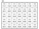
図2は、LED基板101の構成の一例を示す模式図である。LED基板101は、バックライト装置の発光面の領域内の複数の部分領域にそれぞれ対応する複数の発光ブロック111を有する。「バックライト装置の発光面の領域内の複数の部分領域」は、「カラー画像表示装置の画面の領域内の複数の部分領域」と読み替えることができる。図2の例では、LED基板101は、5行×7列のマトリクス状に配置された35個の発光ブロック111を有する。各発光ブロック111の発光輝度は、個別に制御することができる。各発光ブロック111の発光色も、個別に制御することができる。
FIG. 2 is a schematic view showing an example of the configuration of the
各発光ブロック111には、発光色が互いに異なる複数のLED112が設けられている。図2の例では、各発光ブロック111に、2行2列の合計4つのLED112が設けられている。具体的には、各発光ブロックに、1つのR−LED、2つのG−LED、及び、1つのB−LEDが設けられている。R−LEDは、赤色の光を発するLEDであり、G−LEDは、緑色の光を発するLEDであり、B−LEDは、青色の光を発するLEDである。本実施例では、R−LEDとして、インジウム・ガリウム・アルミニウム・リン(InGaAlP)系半導体LEDが使用され、G−LED及びB−LEDとして、ガリウム・ナイトライド(GaN)系半導体LEDが使用される。
Each
各発光ブロック111には、光センサ113(検出部)が設けられている。光センサ113は、発光ブロック111からの光を検出し、検出値(光検出値)を出力する。発光ブロック111からの光の一部は、光学シート(拡散板や反射型偏光フィルム)などで反射され、発光ブロック111の側へ戻される。光センサ113は、例えば、発光ブロック111から直接入射した光(直接光)と、光学シート106で反射されLED基板101の側に戻された光(反射光)と、の合成光を検出する。光センサ113としては、光の輝度を検出する輝度センサ(フォトダイオード、フォトトランジスタ、等)を用いることができる。また、光センサ113として、光の色を検出するカラーセンサを用いることもできる。光センサ113として、光の輝度と色の両方を検出する光センサを用いることもできる。光センサ113の検出値から、LED112の劣化や温度変化に起因した発光ブロック111の発光色と発光輝度の少なくとも一方の変化を判断することができる。
Each
なお、発光ブロック111の数、形状、及び、配置は特に限定されない。1つの発光ブロックがLED基板101として使用されてもよい。例えば、LED基板101では、上記35個の発光ブロック111が1つの発光ブロックとして使用されてもよい。また、複
数の発光ブロック111は、千鳥格子状に配置されていてもよい。図2の例では、正面方向から見た場合の発光ブロック111の形状が四角形であるが、発光ブロック111の形状は、三角形、五角形、六角形、円形、等であってもよい。
The number, shape, and arrangement of the
同様に、部分領域の数、形状、及び、配置も特に限定されない。例えば、画面の領域を構成する複数の分割領域が、複数の部分領域として使用されてもよい。複数の部分領域は互いに離れていてもよいし、部分領域の少なくとも一部が他の部分領域の少なくとも一部に重なっていてもよい。 Similarly, the number, shape, and arrangement of partial areas are not particularly limited. For example, a plurality of divided areas constituting an area of the screen may be used as a plurality of partial areas. The plurality of partial regions may be separated from one another, or at least a portion of the partial region may overlap at least a portion of another partial region.
同様に、LED112の数及び配置も特に限定されない。また、LED112の種類(発光色)も特に限定されない。例えば、黄色の光を発するLEDが使用されてもよい。R−LEDとB−LEDの少なくとも一方が使用されなくてもよい。
Similarly, the number and arrangement of the
同様に、光センサ113の数及び配置も特に限定されない。例えば、2つ以上の発光ブロック111に対して1つの光センサ113が設けられていてもよい。
Similarly, the number and arrangement of the
図3は、正面方向から見た場合の、複数の発光ブロック111の配置の一例を示す模式図である。本実施例では、図3に示すように、X行Y列目(X=1〜5、Y=1〜7)に配置された発光ブロック111を「発光ブロック111(X,Y)」と記載する。例えば、左上隅に配置された発光ブロック111を「発光ブロック111(1,1)」と記載し、右下隅に配置された発光ブロック111を「発光ブロック111(5,7)」と記載する。
FIG. 3 is a schematic view showing an example of the arrangement of the plurality of light emitting
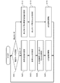
図4は、本実施例に係るカラー画像表示装置の構成の一例を示すブロック図である。まず、入力画像データに基づく画像を表示する際のカラー画像表示装置の動作の一例について説明する。 FIG. 4 is a block diagram showing an example of the configuration of a color image display apparatus according to the present embodiment. First, an example of the operation of the color image display apparatus when displaying an image based on input image data will be described.
モード設定部170は、LED基板101(複数のLED112)の駆動方法が互いに異なる複数の駆動モードのうちのいずれかを、画像処理部160に設定する。具体的には、モード設定部170は、複数の駆動モードのうちのいずれかを示すモード信号171を画像処理部160に出力する。それにより、モード信号171が示す駆動モードが、画像処理部160に設定される。本実施例では、複数の駆動モードは、LDモード(第1モード)と、非LDモード(第2モード)と、を含む。LDモードは、LED基板101の発光輝度と発光色の少なくとも一方を適応的に変化させる駆動モードである。また、LDモードは、複数の部分領域のそれぞれについて、LED基板101の発光輝度と発光色の少なくとも一方を個別に変化させる駆動モードでもある(ローカルディミング制御の実行)。換言すれば、LDモードは、複数の発光ブロック111の発光輝度と発光色の少なくとも一方を個別に変化させる駆動モードである。非LDモードは、LED基板101の発光輝度と発光色を変化させない駆動モードである。また、非LDモードは、複数の部分領域の間でLED基板101の発光輝度と発光色を略一致(完全一致を含む)させる駆動モードでもある。換言すれば、非LDモードは、複数の発光ブロック111の間で発光ブロック111の発光輝度と発光色を略一致させる駆動モードである(ローカルディミング制御の非実行)。
The
画像処理部160は、設定された駆動モードに応じた処理を行う。
The
まず、非LDモードが設定されている場合について説明する。この場合、画像処理部160は、複数の発光ブロック111の間で共通のLD補正値162を決定し、決定したLD補正値162をマイコン125に出力する。LD補正値162は、LED112の発光色毎に決定される。また、画像処理部160は、入力画像データ150に所定の画像処理
を施すことにより、表示画像データ161を生成する。所定の画像処理は、例えば、解像度変換処理、シャープネス処理、色変換処理、ガンマ変換処理、等の一般的な画像処理である。そして、画像処理部160は、生成した表示画像データ161を、カラー液晶パネル105に出力する。なお、入力画像データが表示画像データとして使用されてもよい。
First, the case where the non-LD mode is set will be described. In this case, the
次に、LDモードが設定されている場合について説明する。この場合、画像処理部160は、複数の発光ブロック111のそれぞれについてLD補正値162を個別に決定し、決定したLD補正値162をマイコン125に出力する。LD補正値162は、LED112の発光色と発光ブロック111との組み合わせ毎に決定される。また、画像処理部160は、入力画像データ150にムラ低減処理と上記所定の画像処理とを施すことにより、表示画像データ161を生成する。複数の発光ブロック111の発光を個別に変化させるローカルディミング制御を行うと、表示画像(画面に表示された画像)に、複数の発光ブロック111の間の発光の違いに起因した意図せぬムラ(輝度ムラ(ハロー現象)や色ムラ)が生じることがある。ムラ低減処理は、このようなムラを低減する画像処理である。そして、画像処理部160は、生成した表示画像データを、カラー液晶パネル105に出力する。なお、上記所定の画像処理は行われなくてもよい。
Next, the case where the LD mode is set will be described. In this case, the
LDモードが設定されている場合におけるLD補正値162の決定方法の具体例について説明する。画像処理部160は、複数の部分領域のそれぞれについて、その部分領域に表示すべき画像データの輝度を、入力画像データ150を解析することによって判断する。そして、画像処理部160は、複数の部分領域のそれぞれについて、その部分領域に表示すべき画像データの輝度に応じて、当該部分領域に対応する発光ブロック111のLD補正値162を決定する。例えば、部分領域に表示すべき画像データの輝度が低い発光ブロック111の発光輝度が、部分領域に表示すべき画像データの輝度が高い発光ブロック111の発光輝度に比べ高い値に制御されるように、LD補正値162を決定する。
A specific example of the method of determining the
不揮発性メモリ126には、複数の発光ブロック111のそれぞれについて決定された発光変化補正値163が記録されている。発光変化補正値163は、LED112の発光色と発光ブロック111との組み合わせ毎に決定される。マイコン125は、複数の発光ブロック111のそれぞれについて決定された発光変化補正値163を、不揮発性メモリ126から読み出す。そして、マイコン125は、複数の発光ブロック111のそれぞれについて、画像処理部160から出力されたLD補正値162と、読み出した発光変化補正値163と、に基づいて、LEDドライバ制御信号127を生成する。その後、マイコン125は、発光ブロック111について生成したLEDドライバ制御信号127を、当該発光ブロック111に対応するLEDドライバ120に出力する。図4では、発光ブロック111(X,Y)に対応するLEDドライバ120が、「LEDドライバ120(X,Y)」と記載されている。LEDドライバ120(X,Y)は、入力されたLEDドライバ制御信号127に応じて、発光ブロック111(X,Y)を駆動する。その結果、モード設定部170によって設定された駆動モードに応じた駆動方法で、LED基板101が駆動される。
In the non-volatile memory 126, the light emission change correction value 163 determined for each of the plurality of light emission blocks 111 is recorded. The light emission change correction value 163 is determined for each combination of the light emission color of the
次に、発光変化補正値163を生成する際のカラー画像表示装置の動作の一例について説明する。複数のLED112の温度および経年劣化度合いが変化すると、複数のLED112の発光特性が変化する。その結果、LED基板101の発光輝度や発光色の意図せぬ変化が生じる。また、複数のLED112の温度および経年劣化度合いがばらつくと、複数のLED112の発光特性もばらつく。その結果、LED基板101から意図せぬムラ(輝度ムラや色ムラ)のある光が発せられてしまう。発光変化補正値163は、LED基板101から発せられた光の意図せぬ変化やムラを低減する補正値である。本実施例では、定期的もしくは特定のタイミングで、以下の処理(発光変化補正値163を生成する処理;発光調整処理)が行われる。発光調整処理は、ユーザがカラー画像表示装置を使用
していない空き時間に行われてもよいし、そうでなくてもよい。ユーザがカラー画像表示装置を使用している最中に、発光調整処理の実行による表示画像の画質の変化がユーザに視認されないように、短時間で行われてもよい。
Next, an example of the operation of the color image display apparatus when generating the light emission change correction value 163 will be described. When the temperature and the degree of deterioration of the plurality of
発光調整処理では、処理対象の発光ブロック111(対象ブロック)のみが点灯され、それ以外の発光ブロック111が消灯される。その状態で、対象ブロックから発せられた光が光センサ113を用いて検出される。そして、光センサ113の検出値に基づいて発光変化補正値163が決定され、決定した発光変化補正値163を用いて対象ブロックの発光輝度や発光色が調整される。また、決定した発光変化補正値163が不揮発性メモリ126に記録される。このような処理が、複数の発光ブロック111のそれぞれについて行われる。以下では、発光ブロック111(3,4)が対象ブロックである場合の例を説明する。また、以下では、発光ブロック111の発光輝度を調整する例を説明する。
In the light emission adjustment process, only the light emission block 111 (target block) to be processed is turned on, and the other light emission blocks 111 are turned off. In that state, the light emitted from the target block is detected using the
各光センサ113では、発光ブロック111(3,4)から発せられた光121(3,4)が検出される。各光センサ113は、検出した光121(3,4)の輝度に応じて、当該輝度を表すアナログ値122(検出値)を出力する。図4では、発光ブロック111(X,Y)に対応する光センサ113が、「光センサ113(X,Y)」と記載されており、光センサ113(X,Y)から出力されたアナログ値122が、「アナログ値122(X,Y)」と記載されている。A/Dコンバータ123は、各光センサ113が出力したアナログ値122のうち、発光ブロック111(3,4)に対応付けられている光センサ113(3,4)が出力したアナログ値122(3,4)を選択する。そして、A/Dコンバータ123は、選択したアナログ値をデジタル値にアナログ−デジタル変換し、デジタル値124をマイコン125に出力する。マイコン125は、光センサ113(3,4)の検出値に基づいて、発光ブロック111(3,4)の発光変化補正値163を生成(決定;算出)する。具体的には、マイコン125は、アナログ値122(3,4)を変換して得られたデジタル値124に基づいて、発光ブロック111(3,4)の発光変化補正値163を生成する。そして、マイコン125は、生成した発光変化補正値163を不揮発性メモリ126に記録する。
In each
不揮発性メモリ126には、カラー画像表示装置の製造時に決定した各発光ブロック111の輝度基準値(検出値の基準値)が予め記録されている。マイコン125は、対象ブロックの検出値と、対象ブロックの輝度基準値とを比較する。そして、マイコン125は、上記比較の結果に応じて、対象ブロックの検出値が対象ブロックの輝度基準値と一致するように、対象ブロックの発光変化補正値163を決定する。発光変化補正値163は、LEDドライバ制御信号127を調整する補正値である。発光ブロック111の発光輝度は、発光ブロック111に印加するパルス信号(電流または電圧のパルス信号)のパルス幅やパルス振幅を調整することで調整することができる。発光変化補正値163は、パルス幅を変更する補正値であってもよいし、パルス振幅を変更する補正値であってもよいし、パルス幅とパルス振幅の両方を変更する補正値であってもよい。
In the non-volatile memory 126, the luminance reference value (the reference value of the detection value) of each light-emitting
検出値が基準値となるように各発光ブロック111の発光輝度を調整する発光変化補正値163を決定し、決定した発光変化補正値163を使用することにより、LED基板101から発せられた光の意図せぬ変化やムラを低減することができる。
By determining the light emission change correction value 163 for adjusting the light emission luminance of each
図5は、本実施例に係るカラー画像表示装置の処理フローの一例を示すフローチャートである。以下、図5を用いて、本実施例に係るカラー画像表示装置の処理フローの一例について説明する。 FIG. 5 is a flow chart showing an example of the processing flow of the color image display apparatus according to this embodiment. Hereinafter, an example of the processing flow of the color image display apparatus according to the present embodiment will be described with reference to FIG.
まず、モード設定部170が、駆動モードを設定する(S101)。LDモードが設定された場合には、S102に処理が進められ、非LDモードが設定された場合には、S1
12に処理が進められる。モード設定部170は、ユーザ操作に応じて駆動モードを設定する。ユーザ操作は、例えば、複数の駆動モードのリストから1つの駆動モードを選択するユーザ操作である。リストとしては、例えば、OSD(On Screen Display)画像が使用される。駆動モードの設定方法は特に限定されない。例えば、モード設定部170は、入力画像データ150に応じて自動で駆動モードを設定(変更)してもよい。表示画像のコントラストを高めたい場合に、LDモードが設定される。
First, the
Processing proceeds to 12. The
S102では、マイコン125が、発光ブロック111の点灯期間に発光ブロック111に供給する電流の値(駆動電流値)の基準値である基準電流値を設定する。本実施例では、LDモード時に、発光ブロック111に供給するパルス電流のパルス幅が、入力画像データ150に応じて制御される。パルス幅の制御は、「PWM制御」と呼ばれる。そのため、S102の処理は、発光ブロック111の点灯期間に発光ブロック111に供給する電流の値を決定する処理でもある。
In S102, the
本実施例では、発光ブロック111は周期的に発光する。S102の次に、マイコン125は、発光ブロック111の発光の1周期における発光ブロック111の点灯期間の長さを示すDuty比の基準値である基準Duty比を設定する(S103)。本実施例では、Duty比は、1周期の長さに対する点灯期間の長さの比である。マイコン125は、例えば、表示輝度(画面上の輝度)の基準値である基準輝度に応じて基準Duty比を決定する。本実施例では、基準輝度は、100[cd/m2]である。表示輝度は、駆動電流値とDuty比とに依存する。表示輝度を1/2に低減したい場合には、例えば、Duty比を1/2倍すればよい。
In the present embodiment, the
なお、基準輝度は、予め定められた固定値であってもよいし、ユーザが変更可能な値であってもよい。基準輝度は、100[cd/m2]より高くても低くてもよい。また、Duty比の定義は特に限定されない。例えば、1周期の長さに対する消灯期間の長さの比がDuty比として使用されてもよい。 The reference luminance may be a predetermined fixed value or a value changeable by the user. The reference luminance may be higher or lower than 100 [cd / m 2 ]. Also, the definition of the duty ratio is not particularly limited. For example, the ratio of the length of the light off period to the length of one cycle may be used as the duty ratio.
図6は、基準電流値と基準Duty比の一例を示すグラフである。本実施例では、複数のLED112のそれぞれが周期的に発光する。そして、図6に示すように、複数のLED112のそれぞれについて基準電流値と基準Duty比が設定される。基準電流値と基準Duty比は、例えば、画面全体に渡って白色の画像を基準輝度で表示する場合などに使用される。
FIG. 6 is a graph showing an example of the reference current value and the reference duty ratio. In the present embodiment, each of the plurality of
図6の例では、R−LED、G−LED、及び、B−LEDの全てのLEDについて同じ基準電流値と基準Duty比が示されているが、これに限らない。一般的には、R−LED、G−LED、及び、B−LEDの間で、基準電流値と基準Duty比は異なる。例えば、LED基板101から発せられる光の色温度が調整されると、R−LEDの基準電流値と基準Duty比、G−LEDの基準電流値と基準Duty比、及び、B−LEDの基準電流値と基準Duty比が個別に調整される。また、一般的には、複数の発光ブロック111の間で、基準電流値と基準Duty比は異なる。
Although the example of FIG. 6 shows the same reference current value and reference duty ratio for all the LEDs of R-LED, G-LED, and B-LED, it is not limited thereto. Generally, the reference current value and the reference duty ratio are different between the R-LED, the G-LED, and the B-LED. For example, when the color temperature of light emitted from the
LDモード時には、入力画像データ150に応じて発光ブロック111の発光輝度や発光色が変更される。そのため、発光ブロック111の発光輝度の伸びしろを設ける必要があり、基準Duty比は低めに設定される。例えば、Duty比の上限値の25%程度が基準Duty比として設定される。一方、設定された基準輝度での表示を可能とするために、基準電流値は高めに設定される。例えば、100[mA]程度が基準電流値として設定される。また、基準電流値と基準Duty比を決定する際には、発光変化補正値163が使用される。
In the LD mode, the light emission luminance and the light emission color of the
図7は、Duty比、駆動電流値、及び、点灯サイクルの関係の一例を示すグラフである。各LED112は、例えば、48〜600[Hz]程度の点灯サイクルで繰り返し発光する。点灯サイクルの周波数が600[Hz]である場合、各LED112の発光の1周期の長さは、約1.67[ms]である。Duty比が25%である場合、1周期におけるLED112の点灯期間の長さは、約0.42msである。
FIG. 7 is a graph showing an example of the relationship between the duty ratio, the drive current value, and the lighting cycle. Each
図5の説明に戻る。S103の次に、マイコン125は、入力画像データ150に応じて、各発光ブロック111のDuty比を設定する(S104)。具体的には、画像処理部160から出力されたLED補正値162を用いて基準Duty比を調整することにより、発光ブロック111のDuty比が決定される。そして、マイコン125は、S102で設定された基準電流値と、S104で設定されたDuty比と、に従って、LED基板101を駆動する(S105)。
It returns to the explanation of FIG. After S103, the
図8は、対応する部分領域に表示すべき画像が明るい画像である発光ブロック111のDuty比の一例を示すグラフである。表示すべき画像が明るい場合、1周期における点灯期間が基準Duty比よりも長いDuty比が設定される。本実施例では、基準Duty比よりも高いDuty比が設定される。例えば、90%のDuty比が設定される。基準Duty比が25%であったとすると、Duty比が90%の発光ブロック111は、Duty比が基準Duty比と同じ値であった場合の発光輝度の約3.6倍の発光輝度で発光する。明るい画像の領域は、例えば、夜空に輝く月の領域などである。
FIG. 8 is a graph showing an example of the duty ratio of the
図9は、対応する部分領域に表示すべき画像が暗い画像である発光ブロック111のDuty比の一例を示すグラフである。表示すべき画像が暗い場合、1周期における点灯期間が基準Duty比よりも短いDuty比が設定される。本実施例では、基準Duty比よりも低いDuty比が設定される。例えば、8%のDuty比が設定される。基準Duty比が25%であったとすると、Duty比が8%の発光ブロック111は、Duty比が基準Duty比と同じ値であった場合の発光輝度の約0.3倍の発光輝度で発光する。暗い画像の領域は、例えば、花火の背景となる夜空の領域などである。
FIG. 9 is a graph showing an example of the duty ratio of the
S104とS105の処理は、例えば、入力画像データ150のフレーム毎に繰り返し行われる。S105の次に、S101に処理が戻される。そして、LDモードが設定されている間、S102〜S105の処理が繰り返し行われ、非LDモードが設定されると、S112に処理が進められる。
The processes of S104 and S105 are repeatedly performed, for example, for each frame of the
S112では、マイコン125が、非LDモード用の駆動電流値を設定する。次に、マイコン125は、非LDモード用のDuty比を設定する(S113)。S112とS113では、S102〜104と同様に、複数のLED112のそれぞれについて、駆動電流値とDuty比とが設定される。S112とS113では、発光ブロック111の発光輝度及び発光色が、LDモードが設定されているときのそれらと略一致するように、駆動電流値とDuty比とが設定される。そして、マイコン125は、S112で設定された駆動電流値と、S113で設定されたDuty比と、に従って、LED基板101を駆動する。
At S112, the
図10は、S112とS113で設定された駆動電流値とDuty比の一例を示すグラフである。図10に示すように、本実施例では、G−LEDの駆動電流値は基準電流値よりも低い。そして、G−LEDのDuty比は基準Duty比よりも低い。換言すれば、G−LEDの発光の1周期における当該G−LEDの点灯期間は、基準Duty比よりも長い。具体的には、R−LEDとB−LEDについては、基準電流値と同じ駆動電流値(100[mA])、及び、基準Duty比と同じDuty比(25%)が設定されている。そして、G−LEDについては、基準電流値の1/4である25[mA]が駆動電流値
として設定されており、基準Duty比の2倍である50%がDuty比として設定されている。G−LEDの電力効率は、駆動電流値を下げることで大きく改善される。そのため、G−LEDの駆動電流値とDuty比として図10に示す値を用いることにより、装置全体の消費電力を低減することができる。具体的には、G−LEDの駆動電流値を100[mA]から25[mA]に、G−LEDのDuty比を25%から50%に変更することにより、G−LEDの発光輝度の変化を抑制しつつ、G−LEDの消費電力を約半分に低減することができる。なお、R−LEDとB−LEDの駆動電流値は基準電流値と異なっていてもよいし、R−LEDとB−LEDのDuty比は基準Duty比と異なっていてもよい。
FIG. 10 is a graph showing an example of the drive current value and the duty ratio set in S112 and S113. As shown in FIG. 10, in the present embodiment, the drive current value of the G-LED is lower than the reference current value. And, the duty ratio of the G-LED is lower than the reference duty ratio. In other words, the lighting period of the G-LED in one cycle of the light emission of the G-LED is longer than the reference duty ratio. Specifically, for R-LED and B-LED, the same drive current value (100 [mA]) as the reference current value and the same duty ratio (25%) as the reference duty ratio are set. Then, for the G-LED, 25 [mA] which is 1⁄4 of the reference current value is set as the drive current value, and 50% which is twice the reference duty ratio is set as the duty ratio. The power efficiency of the G-LED is greatly improved by lowering the drive current value. Therefore, the power consumption of the entire device can be reduced by using the values shown in FIG. 10 as the drive current value and the duty ratio of the G-LED. Specifically, by changing the drive current value of G-LED from 100 [mA] to 25 [mA] and changing the duty ratio of G-LED from 25% to 50%, the change in emission luminance of G-LED The power consumption of the G-LED can be reduced to about half while suppressing the The driving current value of the R-LED and the B-LED may be different from the reference current value, and the duty ratio of the R-LED and the B-LED may be different from the reference duty ratio.
以下で、S112〜S115の処理を行うことで電力効率が改善されることを説明する。 Hereinafter, it will be described that the power efficiency is improved by performing the processes of S112 to S115.
図11は、LED112の駆動電流値Ifと順方向電圧Vfの関係の一例を示すグラフである。図11の横軸は駆動電流値Ifを示し、図11の縦軸は順方向電圧Vfを示す。実線301はR−LEDの特性を示し、破線302はG−LEDとB−LEDの特性を示す。
FIG. 11 is a graph showing an example of the relationship between the drive current value If of the
R−LEDでは、実線301のように、駆動電流値Ifの低下に伴う順方向電圧Vfの低下はそれほど大きくない。一方、G−LEDやB−LEDでは、破線302のように、駆動電流値Ifの低下に伴う順方向電圧Vfの低下が大きい。LEDで消費される電力は、駆動電流値Ifに順方向電圧Vfを乗算することで算出される。そのため、G−LEDとB−LEDでは、駆動電流値Ifの低下によって、順方向電圧Vfが大きく低下し、消費電力が大幅に低減される。
In the R-LED, as indicated by the
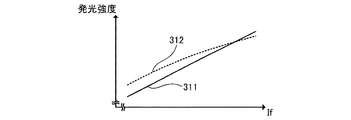
図12は、LED112の駆動電流値Ifと発光強度(発光輝度の瞬時値)の関係の一例を示すグラフである。図12の横軸は駆動電流値Ifを示し、図12の縦軸は発光強度を示す。実線311はR−LEDとB−LEDの特性を示し、破線312はG−LEDの特性を示す。
FIG. 12 is a graph showing an example of the relationship between the drive current value If of the
R−LEDとB−LEDでは、駆動電流値Ifの低下に伴う発光強度の低下が大きい。そのため、R−LEDとB−LEDでは、駆動電流値Ifの低下に伴う発光輝度の低下を抑制するために、長い点灯期間が必要となる。一方、G−LEDでは、駆動電流値Ifの低下に伴う発光強度の低下がそれほど大きくない。これは、駆動電流値Ifの低下に伴い、量子効率が改善されるためである。そのため、G−LEDでは、点灯期間をそれほど延ばさずに、駆動電流値Ifの低下に伴う発光輝度の低下を抑制することができる。 In the R-LED and the B-LED, the decrease of the light emission intensity is large with the decrease of the drive current value If. Therefore, in the R-LED and the B-LED, a long lighting period is required in order to suppress the decrease in light emission luminance due to the decrease in the drive current value If. On the other hand, in the G-LED, the decrease of the light emission intensity accompanying the decrease of the drive current value If is not so large. This is because the quantum efficiency is improved as the drive current value If decreases. Therefore, in the G-LED, it is possible to suppress the decrease in the light emission luminance due to the decrease in the drive current value If without extending the lighting period so much.
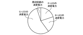
図13は、LED基板101の消費電力の内訳の一例を示す円グラフである。図13は、LED基板101から白色光が発せられるように各LED112の発光輝度が調整されている場合の例を示す。
FIG. 13 is a pie chart showing an example of the breakdown of the power consumption of the
図13から、G−LEDの消費電力が最も大きいことがわかる。具体的には、全体の消費電力に対するG−LEDの消費電力の割合は、55%程度である。これは、R−LEDやB−LEDと比較してG−LEDの発光効率が低いためである。例えば、G−LEDの発光効率は、G−LEDと同じGaN系半導体であるB−LEDの約半分以下であると言われている。R−LEDの消費電力の割合、及び、B−LEDの消費電力の割合は、それぞれ、20%程度である。LED以外の周辺回路の消費電力は5%程度である。このことから、G−LEDの消費電力の大きな低下が、装置全体の消費電力の大きな低下をもたらすことがわかる。 It can be seen from FIG. 13 that the power consumption of the G-LED is the largest. Specifically, the ratio of the power consumption of the G-LED to the total power consumption is about 55%. This is because the light emission efficiency of the G-LED is lower than that of the R-LED or the B-LED. For example, it is said that the luminous efficiency of the G-LED is about half or less of that of the B-LED, which is the same GaN-based semiconductor as the G-LED. The ratio of the power consumption of the R-LED and the ratio of the power consumption of the B-LED are each approximately 20%. The power consumption of peripheral circuits other than the LED is about 5%. From this, it can be seen that a large reduction in power consumption of the G-LED results in a large reduction in power consumption of the entire device.
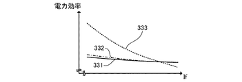
図14は、LED112の駆動電流値IfとLED基板101の電力効率との関係の一例を示すグラフである。図14の横軸は駆動電流値Ifを示し、図14の縦軸は電力効率を示す。図14に示す特性は、図11〜13に示す特性に基づいて決定されたものである。図14の電力効率は、LED基板101全体の電力効率であり、単位電力当たりの発光輝度を意味する。
FIG. 14 is a graph showing an example of the relationship between the drive current value If of the
実線331は、R−LEDの特性を示す。図11,12に示すように、R−LEDでは、駆動電流値Ifの低下に伴う順方向電圧Vfの低下が小さく、駆動電流値Ifの低下に伴う発光強度の低下が大きい。また、図13に示すように、LED基板101全体の消費電力に対するR−LEDの消費電力の割合が小さい。以上のことから、実線331に示すように、駆動電流値Ifの低下に伴う電力効率の向上は非常に小さい。
The
一点鎖線332は、B−LEDの特性を示す。図11に示すように、B−LEDでは、駆動電流値Ifの低下に伴う順方向電圧Vfの低下が大きい。しかしながら、図12に示すように、駆動電流値Ifの低下に伴う発光強度の低下が大きい。また、図13に示すように、LED基板101全体の消費電力に対するB−LEDの消費電力の割合が小さい。以上のことから、一点鎖線332に示すように、駆動電流値Ifの低下に伴う電力効率の向上は小さい。
An alternate long and
破線333は、G−LEDの特性を示す。図11,12に示すように、G−LEDでは、駆動電流値Ifの低下に伴う順方向電圧Vfの低下が大きく、駆動電流値Ifの低下に伴う発光強度の低下が小さい。また、図13に示すように、LED基板101全体の消費電力に対するG−LEDの消費電力の割合が大きい。以上のことから、破線333に示すように、駆動電流値Ifの低下に伴う電力効率の向上は非常に大きい。
The
以上のことから、図10に示すように、G−LEDの駆動電流値を下げ、且つ、G−LEDのDuty比を上げることで、装置全体の消費電力を大幅に低減することができる。なお、本実施例では、図10に示すように、B−LEDについては、G−LEDと同様の処理を行っていない。これは、B−LEDの電流量を下げ、且つ、B−LEDのDuty比を上げる処理による電力効率の向上よりも、当該処理に起因したB−LEDの経年劣化の加速が大きいためである。 From the above, as shown in FIG. 10, the power consumption of the entire device can be significantly reduced by decreasing the drive current value of the G-LED and increasing the duty ratio of the G-LED. In the present embodiment, as shown in FIG. 10, processing similar to that of G-LED is not performed for B-LED. This is because the acceleration of aging of the B-LED due to the process is larger than the improvement of the power efficiency by the process of reducing the current amount of the B-LED and increasing the duty ratio of the B-LED.
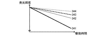
図15は、LED112の駆動時間とLED112の発光輝度との関係(経年劣化特性)の一例を示すグラフである。図15の横軸はLED112の駆動時間を示し、図15の縦軸はLED112の発光輝度を示す。図15に示す発光輝度は、駆動時間が0のときの発光輝度で正規化された値である。
FIG. 15 is a graph showing an example of the relationship between the driving time of the
経年によって生じるLEDの発光輝度の低下は、LEDの発光色や使用条件に大きく依存する。図15の太実線341は、B−LEDを駆動電流値50[mA]とDuty比50%で使用し続けた場合のB−LEDの経年劣化特性を示す。細実線342は、B−LEDを駆動電流値100[mA]とDuty比25%で使用し続けた場合のB−LEDの経年劣化特性を示す。太破線343は、G−LEDを駆動電流値50[mA]とDuty比50%で使用し続けた場合のG−LEDの経年劣化特性を示す。細破線344は、G−LEDを駆動電流値100[mA]とDuty比25%で使用し続けた場合のG−LEDの経年劣化特性を示す。
The decrease in the emission brightness of the LED caused by the aging largely depends on the emission color of the LED and the use conditions. The thick
LEDの経年劣化は、発光波長(LEDが発する光の波長)、Duty比、及び、チップ温度(LEDの温度)に依存する。発光波長が短いほど、経年劣化の速度は速い。Duty比が高いほど、経年劣化の速度は速い。そして、チップ温度が高いほど、経年劣化の速度は速い。B−LEDの発光波長は短いため、太実線341と細実線342のように、
経年劣化の速度が非常に速い。また、駆動電流値を下げ、且つ、Duty比を上げる処理により、経年劣化は加速する。このことから、B−LEDの駆動電流値を下げ、且つ、B−LEDのDuty比を上げる処理を行った場合に、電力効率の向上よりも、B−LEDの経年劣化の加速のほうが大きいことが分かる。G−LEDの発光波長はB−LEDに比べ長いため、太破線343と細破線344のように、経年劣化の速度は比較的遅い。G−LEDの駆動電流値を下げ、且つ、G−LEDのDuty比を上げる処理により、G−LEDの経年劣化が加速する可能性がある。しかしながら、そのような処理によって、電力効率が大きく向上する。その結果、G−LEDの温度の低下が期待でき、G−LEDの経年劣化の加速に対する懸念は少ない。
Aging of the LED depends on the light emission wavelength (the wavelength of the light emitted by the LED), the duty ratio, and the chip temperature (the temperature of the LED). As the emission wavelength is shorter, the rate of aging is faster. The higher the duty ratio, the faster the aging rate. And, the higher the chip temperature, the faster the aging rate. Since the emission wavelength of B-LED is short, as shown by thick
The rate of aging is very fast. Further, the aging deterioration is accelerated by the process of decreasing the drive current value and increasing the duty ratio. From this, when processing is performed to lower the drive current value of the B-LED and increase the duty ratio of the B-LED, acceleration of aging of the B-LED is larger than improvement of the power efficiency. I understand. Since the emission wavelength of the G-LED is longer than that of the B-LED, the rate of aging is relatively slow, as indicated by the thick
以上述べたように、本実施例によれば、以下の仮定において、第2モード(非LDモード)では、第1モード(LDモード)に比べ、G−LEDの駆動電流値が低く、G−LEDの点灯期間が長い。それにより、ローカルディミング制御を行わずに光源装置の消費電力を低減できる。以下の仮定の状況は、例えば、「第1モードが設定されているときにG−LEDが図6に示す基準電流値と基準Duty比で駆動され、第2モードが設定されているときにG−LEDが図10に示す駆動電流値とDuty比で駆動される」という状況である。本実施例では、以下の仮定(第1の仮定)の成立時に「第1モードと第2モードの間でLED基板101の発光輝度及び発光色が略一致するようにLED基板101が駆動される」という仮定(第2の仮定)も成立する。しかしながら、第1の仮定の成立時に第2の仮定が成立しなくてもよい。
仮定:第1モードと第2モードの間でG−LEDの発光輝度が略一致するようにG−LEDが駆動される。
As described above, according to this embodiment, in the second mode (non-LD mode), the drive current value of the G-LED is lower in the second mode (non-LD mode) than in the first mode (LD mode). The lighting period of the LED is long. Thus, the power consumption of the light source device can be reduced without performing the local dimming control. The following hypothetical situation, for example, “when the first mode is set, the G-LED is driven with the reference current value and the reference duty ratio shown in FIG. 6, and the second mode is set The LED is driven with the drive current value and the duty ratio shown in FIG. In the present embodiment, the
Assumption: The G-LEDs are driven such that the emission luminances of the G-LEDs substantially match between the first mode and the second mode.
なお、本実施例では、第1モードがLDモードである場合の例を説明したが、これに限らない。例えば、第1モードは、図6の基準電流値と基準Duty比を常に使用する駆動モードであってもよい。また、ローカルディミング制御において、駆動電流値が入力画像データに応じて変更されてもよいし、駆動電流値とDuty比が入力画像データに応じて変更されてもよい。 In the present embodiment, although the example in which the first mode is the LD mode has been described, the present invention is not limited to this. For example, the first mode may be a drive mode that always uses the reference current value and the reference duty ratio of FIG. Further, in the local dimming control, the drive current value may be changed according to the input image data, or the drive current value and the duty ratio may be changed according to the input image data.
<実施例2>
以下、本発明の実施例2に係る光源装置、表示装置、及び、それらの制御方法について説明する。実施例1では、第1モードがLDモードであり、第2モードが非LDモードである場合の例を説明した。本実施例では、第1モードが非ブーストモードであり、第2モードがブーストモードである場合の例を説明する。本実施例の非ブーストモードは、実施例1のLDモードと同じである。ブーストモードは、非ブーストモードが設定されているときのLED基板101の発光輝度の上限値よりも高い発光輝度でLED基板101を発光させる駆動モードである。ブーストモードを設定することにより、表示輝度を向上することができる。表示輝度が向上すると、明るい環境下(日中のリビングや屋外など)での表示画像の視認性が向上する。また、ブーストモードを設定することにより、識別可能な階調数が増加するため、マンモグラフィ等の医療用途においても、ブーストモードは好ましい。以下では、実施例1と異なる機能や処理について詳しく説明し、実施例1と同じ機能や処理についての説明は省略する。
Example 2
Hereinafter, a light source device, a display device, and control methods thereof according to a second embodiment of the present invention will be described. In the first embodiment, an example in which the first mode is the LD mode and the second mode is the non-LD mode has been described. In this embodiment, an example in which the first mode is the non-boost mode and the second mode is the boost mode will be described. The non-boost mode of this embodiment is the same as the LD mode of the first embodiment. The boost mode is a drive mode for causing the
なお、非ブーストモードとして、LED基板101の発光輝度と発光色を変化させない駆動モードを使用することもできる。その場合には、ブーストモードは、「非ブーストモードが設定されているときのLED基板101の発光輝度よりも高い発光輝度でLED基板101を発光させる駆動モード」と言える。
As the non-boost mode, a drive mode in which the light emission luminance and the light emission color of the
図16は、本実施例に係るカラー画像表示装置の処理フローの一例を示すフローチャートである。以下、図16を用いて、本実施例に係るカラー画像表示装置の処理フローの一
例について説明する。
FIG. 16 is a flow chart showing an example of the processing flow of the color image display apparatus according to this embodiment. Hereinafter, an example of the processing flow of the color image display apparatus according to the present embodiment will be described with reference to FIG.
まず、モード設定部170が、駆動モードを設定する(S201)。非ブーストモードが設定された場合には、S202に処理が進められ、ブーストモードが設定された場合には、S212に処理が進められる。モード設定部170は、ユーザ操作に応じて駆動モードを設定する。ユーザ操作は、例えば、複数の駆動モードのリストから1つの駆動モードを選択するユーザ操作である。駆動モードの設定方法は特に限定されない。例えば、モード設定部170は、複数の駆動モードのいずれかを選択するユーザ操作以外のユーザ操作に応じて、駆動モードを設定してもよい。具体的には、モード設定部170は、ユーザが入力した基準輝度が閾値(例えば100[cd/m2])以上であるか否かに応じて、非ブーストモードとブーストモードの間で駆動モードを切り替えてもよい。LED基板101の発光輝度の上限値や表示輝度の上限値を高めたい場合に、ブーストモードが設定される。
First, the
非ブーストモードが設定されているときのLED基板101の発光輝度と、ブーストモードが設定されているときのLED基板101の発光輝度とは特に限定されない。例えば、非ブーストモードが設定されているときのLED基板101の発光輝度の上限値は100[cd/m2]であり、ブーストモードが設定されているときのLED基板101の発光輝度はその2倍(200[cd/m2])である。各駆動モードにおけるLED基板101の発光輝度(の上限値)は、予め定められた固定値であってもよいし、ユーザが変更可能な値であってもよい。
The light emission luminance of the
S202〜S205では、実施例1(図5)のS102〜S105と同じ処理が行われる。 In S202 to S205, the same processing as S102 to S105 of the first embodiment (FIG. 5) is performed.
S212では、マイコン125が、ブーストモード用の駆動電流値を設定する。次に、マイコン125は、ブーストモード用のDuty比を設定する(S213)。本実施例では、実施例1と同様の観点にしたがって、ブーストモード用の駆動電流値とDuty比が設定される。但し、本実施例では、実施例1の非LDモードよりも高い発光輝度でLED基板101が発光するように、駆動電流値とDuty比の少なくとも一方として、図10よりも高い値が設定される。そして、マイコン125は、S112で設定された駆動電流値と、S113で設定されたDuty比と、に従って、LED基板101を駆動する(S215)。
At S212, the
以上述べたように、本実施例によれば、実施例1と同様に、実施例1で述べた仮定において、第2モード(ブーストモード)では、第1モード(非ブーストモード)に比べ、G−LEDの駆動電流値が低く、G−LEDの点灯期間が長い。それにより、ローカルディミング制御を行わずに光源装置の消費電力を低減できる。 As described above, according to the present embodiment, as in the first embodiment, under the assumption described in the first embodiment, in the second mode (boost mode), G is greater than in the first mode (non-boost mode). -The driving current value of the LED is low, and the lighting period of the G-LED is long. Thus, the power consumption of the light source device can be reduced without performing the local dimming control.
<実施例3>
以下、本発明の実施例3に係る光源装置、表示装置、及び、それらの制御方法について説明する。実施例1,2では、G−LEDの駆動電流値とDuty比を工夫することで、装置全体の消費電力を低減する例を説明した。しかしながら、LEDの発光波長(主波長λd)は、LEDの駆動電流値に応じて変化する。そのため、G−LEDと他のLEDとの間の駆動電流値のバランスを変える実施例1では、LED基板101の発光色の変化(色ずれ)が生じてしまう。本実施例では、このような色ずれを低減することができる例について説明する。以下では、実施例1と異なる機能や処理について詳しく説明し、実施例1と同じ機能や処理についての説明は省略する。なお、以下では、実施例1をベースとして説明するが、本実施例の処理は実施例2にも適用可能である。
Example 3
Hereinafter, a light source device, a display device, and control methods thereof according to a third embodiment of the present invention will be described. In the first and second embodiments, an example has been described in which the power consumption of the entire device is reduced by devising the drive current value and the duty ratio of the G-LED. However, the emission wavelength (main wavelength λd) of the LED changes in accordance with the drive current value of the LED. Therefore, in Example 1 which changes the balance of the drive current value between G-LED and another LED, the change (color shift) of the luminescent color of
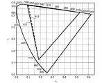
図17は、実施例1に係る表示色(画面上の色)の範囲の一例を示す色度図である。図17は、u’v’色度図(CIE 1976 UCS色度図)である。実線で描かれた三角形401は、LDモードが設定されているときの表示色の範囲を示し、破線で描かれた三角形402は、非LDモードが設定されているときの表示色の範囲を示す。
FIG. 17 is a chromaticity diagram illustrating an example of the range of display colors (colors on the screen) according to the first embodiment. FIG. 17 is a u'v 'chromaticity diagram (CIE 1976 UCS chromaticity diagram). A
三角形401,402の3つの頂点は、赤色の色度点、緑色の色度点、及び、青色の色度点である。ここでは、画像データの画素値がRGB値(R値,G値,B値)であり、各階調値(R値、G値、及び、B値)が0〜255の値であるとする。赤色の色度点は、RGB値(255,0,0)の表示色の色度点であり、(u’,v’)=(0.5,0.5)付近の頂点である。緑色の色度点は、RGB値(0,255,0)の表示色の色度点であり、(u’,v’)=(0.1,0.6)付近の頂点である。青色の色度点は、RGB値(0,0,255)の表示色の色度点であり、(u’,v’)=(0.2,0.1)付近の頂点である。
The three vertices of the
実施例1の非LDモードでは、G−LEDの駆動電流値のみが、LDモードと比較して小さい値に制御される。そのため、非LDモードでは、G−LEDの発光波長λdが、LDモードと比較して長波長側にずれた値となる。例えば、G−LEDの発光波長λdは+4nmだけずれる。LDモードが設定されているときのG−LEDの発光波長λdが530[nm]であった場合には、非LDモードが設定されているときのG−LEDの発光波長λdは534[nm]となる。その結果、三角形402のように、緑色の色度点として、三角形401よりも長波長側にずれた色度点が得られる。また、G−LEDの発光波長λdが長波長側にずれることで、青色の色度点が短波長側にずれる。これは、青色の表示時に漏れ出る緑色光のスペクトルが低減されるからである。このように、実施例1の方法では、LDモードと非LDモードの間で、緑色の色度点と青色の色度点の2点のずれが生じる。そして、このような2点のずれが生じると、表示色及びその範囲に大きな変化(誤差)が生じる。
In the non-LD mode of the first embodiment, only the drive current value of the G-LED is controlled to a small value as compared with the LD mode. Therefore, in the non-LD mode, the emission wavelength λd of the G-LED has a value shifted to the long wavelength side as compared with the LD mode. For example, the emission wavelength λd of the G-LED is shifted by +4 nm. When the light emission wavelength λd of the G-LED when the LD mode is set is 530 nm, the light emission wavelength λd of the G-LED when the non-LD mode is set is 534 nm It becomes. As a result, as the
図18は、本実施例に係る非LDモード用の駆動電流値とDuty比の一例を示すグラフである。図18に示すように、本実施例では、B−LEDの駆動電流値として基準電流値よりも低い値が設定され、B−LEDのDuty比として基準Duty比よりも低い値が設定される。R−LEDとG−LEDについては実施例1と同じである。具体的には、B−LEDの駆動電流値として、G−LEDと同じ値25[mA]が設定される。一方、B−LEDのDuty比として、G−LEDよりも高い値が設定される。これは、G−LEDでは駆動電流値を下げることによる電力効率の向上が期待できるが、B−LEDではそれがあまり期待できないからである。 FIG. 18 is a graph showing an example of the drive current value and the duty ratio for the non-LD mode according to the present embodiment. As shown in FIG. 18, in the present embodiment, a value lower than the reference current value is set as the drive current value of the B-LED, and a value lower than the reference duty ratio is set as the Duty ratio of the B-LED. The R-LED and the G-LED are the same as in the first embodiment. Specifically, the same value 25 [mA] as G-LED is set as the drive current value of B-LED. On the other hand, a higher value than the G-LED is set as the duty ratio of the B-LED. This is because the G-LED can be expected to improve the power efficiency by lowering the drive current value, but the B-LED can not expect so much.
図19は、本実施例に係る表示色の範囲の一例を示す色度図である。実線で描かれた三角形411は、LDモードが設定されているときの表示色の範囲を示し、図17の三角形401と同じものである。破線で描かれた三角形412は、本実施例の非LDモードが設定されているときの表示色の範囲を示す。
FIG. 19 is a chromaticity diagram showing an example of the range of display colors according to the present example. A triangle 411 drawn by a solid line indicates a range of display colors when the LD mode is set, and is the same as the
本実施例の非LDモードでは、G−LEDとB−LEDの駆動電流値が、LDモードと比較して小さい値に制御される。そのため、非LDモードでは、G−LEDとB−LEDの発光波長λdが、LDモードと比較して長波長側にずれた値となる。例えば、G−LEDの発光波長λdは+4nmだけずれ、B−LEDの発光波長λdは+2nmだけずれる。その結果、三角形412のように、緑色の色度点として、三角形411よりも長波長側にずれた色度点が得られる。一方、青色の色度点のずれは小さい。これは、G−LEDとB−LEDの両方の発光波長λdが長波長側にずれることで、青色の表示時に漏れ出る緑色光のスペクトルの低減が抑制されるためである。このように、本実施例では、LDモードと非LDモードの間で、緑色の色度点以外の色度点のずれが小さいため、表示色及びそ
の範囲の誤差を低減することができる。
In the non-LD mode of this embodiment, the drive current value of the G-LED and the B-LED is controlled to a smaller value as compared with the LD mode. Therefore, in the non-LD mode, the emission wavelengths λd of the G-LED and the B-LED are shifted to the long wavelength side as compared with the LD mode. For example, the emission wavelength λd of the G-LED shifts by +4 nm, and the emission wavelength λd of the B-LED shifts by +2 nm. As a result, a chromaticity point shifted to a longer wavelength side than the triangle 411 is obtained as the green chromaticity point, as in the
以上述べたように、本実施例によれば、実施例1と同様にG−LEDの発光が制御される。それにより、ローカルディミング制御を行わずに光源装置の消費電力を低減できる。さらに、本実施例によれば、以下の仮定において、第2モード(非LDモード)では、第1モード(LDモード)に比べ、B−LEDの駆動電流値が低く、B−LEDの点灯期間が長い。それにより、駆動電流値の変化に伴うLED基板101の発光色の変化を低減することができる。
仮定:第1モードと第2モードの間でB−LEDの発光輝度が略一致するようにB−LEDが駆動される。
As described above, according to this embodiment, the light emission of the G-LED is controlled as in the first embodiment. Thus, the power consumption of the light source device can be reduced without performing the local dimming control. Furthermore, according to the present embodiment, under the following assumption, in the second mode (non-LD mode), the drive current value of the B-LED is lower than that in the first mode (LD mode), and the lighting period of the B-LED is Is long. As a result, it is possible to reduce the change in the emission color of the
Assumption: The B-LED is driven such that the emission brightness of the B-LED substantially matches between the first mode and the second mode.
<その他の実施例>
本発明は、上述の実施例の1以上の機能を実現するプログラムを、ネットワーク又は記憶媒体を介してシステム又は装置に供給し、そのシステム又は装置のコンピュータにおける1つ以上のプロセッサーがプログラムを読出し実行する処理でも実現可能である。また、1以上の機能を実現する回路(例えば、ASIC)によっても実現可能である。
<Other Embodiments>
The present invention supplies a program that implements one or more functions of the above-described embodiments to a system or apparatus via a network or storage medium, and one or more processors in a computer of the system or apparatus read and execute the program. Can also be realized. It can also be implemented by a circuit (eg, an ASIC) that implements one or more functions.
101:LED基板 111:発光ブロック
125:マイコン 170:モード設定部
101: LED board 111: light emitting block 125: microcomputer 170: mode setting unit
Claims (17)
前記発光手段の駆動方法が互いに異なる第1駆動モードと第2駆動モードを含む複数の駆動モードのいずれかを設定する設定手段と、
前記設定手段によって設定された駆動モードに応じた駆動方法で、前記複数の発光ダイオードのそれぞれが周期的に発光するように、前記発光手段を駆動する制御手段と、
を有し、
前記発光手段を所定の発光輝度で点灯させる場合に、
前記複数の発光ダイオードのうちの一部の発光ダイオードについて、前記第2駆動モードでは、前記第1駆動モードに比べて、点灯期間の駆動電流値が低く、かつ1周期における点灯時間が長い
ことを特徴とする光源装置。 Light emitting means having a plurality of light emitting diodes different in light emission color from each other;
Setting means for setting any one of a plurality of drive modes including a first drive mode and a second drive mode which are different in drive method of the light emitting means;
Control means for driving the light emitting means such that each of the plurality of light emitting diodes periodically emits light by a driving method according to the driving mode set by the setting means;
Have
When the light emitting means is turned on at a predetermined light emission luminance,
Regarding the light emitting diodes of some of the plurality of light emitting diodes, in the second drive mode, the drive current value in the lighting period is lower than in the first drive mode, and the lighting time in one cycle is longer A light source device characterized by
前記第2駆動モードは、前記発光手段の発光輝度と発光色を、入力画像データに応じて変化させない駆動モードである
ことを特徴とする請求項1に記載の光源装置。 The first drive mode is a drive mode in which at least one of the emission brightness and the emission color of the light emitting means is changed according to input image data .
2. The light source device according to claim 1, wherein the second drive mode is a drive mode in which the emission brightness and the emission color of the light emitting unit are not changed according to input image data .
前記第1駆動モードは、前記複数の部分領域のそれぞれについて、前記発光手段の発光輝度と発光色の少なくとも一方を個別に変化させる駆動モードであり、
前記第2駆動モードは、前記複数の部分領域の間で前記発光手段の発光輝度と発光色を略一致させる駆動モードである
ことを特徴とする請求項2に記載の光源装置。 The light emitting means includes the plurality of light emitting diodes for each of a plurality of partial areas in the area of the light emitting surface of the light emitting means,
The first drive mode is a drive mode in which at least one of the light emission luminance and the light emission color of the light emitting unit is individually changed for each of the plurality of partial regions,
The light source device according to claim 2, wherein the second drive mode is a drive mode in which the emission brightness and the emission color of the light emitting means are substantially matched among the plurality of partial regions.
ことを特徴とする請求項2または3に記載の光源装置。 The second drive mode is a drive mode for causing the light emitting means to emit light at a light emission luminance higher than the upper limit value of the light emission luminance of the light emitting means when the first mode is set. The light source device according to 2 or 3.
前記第1駆動モードと前記第2駆動モードの間で前記G−LEDの発光輝度が略一致するように前記G−LEDを駆動したと仮定した場合において、前記第2駆動モードでは、前記第1駆動モードに比べ、前記G−LEDの点灯期間に前記G−LEDに供給する電流が低く、前記G−LEDの発光の1周期における前記G−LEDの点灯期間が長いIf it is assumed that the G-LED is driven such that the emission brightness of the G-LED substantially matches between the first drive mode and the second drive mode, the first drive mode is selected in the second drive mode. Compared to the drive mode, the current supplied to the G-LED during the lighting period of the G-LED is low, and the lighting period of the G-LED in one cycle of light emission of the G-LED is long
ことを特徴とする請求項1〜4のいずれか1項に記載の光源装置。The light source device according to any one of claims 1 to 4, characterized in that:
前記第1駆動モードと前記第2駆動モードの間で前記B−LEDの発光輝度が略一致するように前記B−LEDを駆動したと仮定した場合において、前記第2駆動モードでは、前記第1駆動モードに比べ、前記B−LEDの点灯期間に前記B−LEDに供給する電流が低く、前記B−LEDの発光の1周期における前記B−LEDの点灯期間が長い
ことを特徴とする請求項5に記載の光源装置。 The plurality of light emitting diodes further include a B-LED that is a light emitting diode that emits blue light,
In assuming that the light emission luminance of the B-LED between the first driving mode and the second drive mode by driving the B-LED to be substantially coincident, and in the second drive mode, the first compared to the driving mode, the B-LED lighting period in the B-LED to the low current supplied, the B - claims lighting period of the B-LED in one cycle of the light emission of the LED is characterized in longer The light source device according to 5 .
ことを特徴とする請求項5または6に記載の光源装置。The light source device according to claim 5 or 6, wherein
ことを特徴とする請求項5〜7のいずれか1項に記載の光源装置。The light source device according to any one of claims 5 to 7, characterized in that:
ことを特徴とする請求項6に記載の光源装置。The light source device according to claim 6, characterized in that:
ことを特徴とする請求項1〜9のいずれか1項に記載の光源装置。The light source device according to any one of claims 1 to 9, characterized in that:
ことを特徴とする請求項1〜10のいずれか1項に記載の光源装置。The light source device according to any one of claims 1 to 10, characterized in that:
前記光源装置から発せられた光を入力画像データに基づいて変調することにより、画面に画像を表示する表示手段と、
を有することを特徴とする画像表示装置。 The light source device according to any one of claims 1 to 11 ,
Display means for displaying an image on a screen by modulating light emitted from the light source device based on input image data;
An image display apparatus characterized by having.
ことを特徴とする請求項12に記載の画像表示装置。 The image display apparatus according to claim 12 , wherein the setting unit sets any one of the plurality of drive modes in accordance with the input image data.
ことを特徴とする請求項12に記載の画像表示装置。 The image display apparatus according to claim 12 , wherein the setting unit sets one of the plurality of drive modes in accordance with a user operation.
ことを特徴とする請求項14に記載の画像表示装置。 The image display apparatus according to claim 14 , wherein the user operation is a user operation different from the user operation for selecting any of the plurality of drive modes.
前記発光手段の駆動方法が互いに異なる第1駆動モードと第2駆動モードを含む複数の駆動モードのいずれかを設定する設定ステップと、
前記設定ステップによって設定された駆動モードに応じた駆動方法で、前記複数の発光ダイオードのそれぞれが周期的に発光するように、前記発光手段を駆動する制御ステップと、
を有し、
前記発光手段を所定の発光輝度で点灯させる場合に、
前記複数の発光ダイオードのうちの一部の発光ダイオードについて、前記第2駆動モードでは、前記第1駆動モードに比べて、点灯期間の駆動電流値が低く、かつ1周期における点灯期間が長い
ことを特徴とする光源装置の制御方法。 A control method of a light source device having light emitting means having a plurality of light emitting diodes having different light emission colors, the light source device comprising:
A setting step of setting one of a plurality of drive modes including a first drive mode and a second drive mode which are different in drive method of the light emitting means;
A control step of driving the light emitting means such that each of the plurality of light emitting diodes periodically emits light by a driving method corresponding to the driving mode set in the setting step;
Have
When the light emitting means is turned on at a predetermined light emission luminance,
Regarding the light emitting diodes of some of the plurality of light emitting diodes, in the second drive mode, the drive current value in the lighting period is lower than in the first drive mode, and the lighting period in one cycle is longer Control method of the light source device characterized by
Priority Applications (5)
| Application Number | Priority Date | Filing Date | Title |
|---|---|---|---|
| JP2015064872A JP6501581B2 (en) | 2015-03-26 | 2015-03-26 | Light source device, image display device, and control method of light source device |
| DE102016105288.4A DE102016105288A1 (en) | 2015-03-26 | 2016-03-22 | LIGHT SOURCE DEVICE, IMAGE DISPLAY DEVICE AND CONTROL METHOD FOR LIGHT SOURCE DEVICE |
| US15/078,145 US9966015B2 (en) | 2015-03-26 | 2016-03-23 | Light source apparatus, image display apparatus and control method for light source apparatus |
| US15/946,228 US10210821B2 (en) | 2015-03-26 | 2018-04-05 | Light source apparatus, image display apparatus and control method for light source apparatus |
| US16/239,925 US20190139498A1 (en) | 2015-03-26 | 2019-01-04 | Light source apparatus, image display apparatus and control method for light source apparatus |
Applications Claiming Priority (1)
| Application Number | Priority Date | Filing Date | Title |
|---|---|---|---|
| JP2015064872A JP6501581B2 (en) | 2015-03-26 | 2015-03-26 | Light source device, image display device, and control method of light source device |
Related Child Applications (1)
| Application Number | Title | Priority Date | Filing Date |
|---|---|---|---|
| JP2019037177A Division JP6724196B2 (en) | 2019-03-01 | 2019-03-01 | Light source device, image display device, and method for controlling light source device |
Publications (3)
| Publication Number | Publication Date |
|---|---|
| JP2016184531A JP2016184531A (en) | 2016-10-20 |
| JP2016184531A5 JP2016184531A5 (en) | 2018-04-12 |
| JP6501581B2 true JP6501581B2 (en) | 2019-04-17 |
Family
ID=56890245
Family Applications (1)
| Application Number | Title | Priority Date | Filing Date |
|---|---|---|---|
| JP2015064872A Expired - Fee Related JP6501581B2 (en) | 2015-03-26 | 2015-03-26 | Light source device, image display device, and control method of light source device |
Country Status (3)
| Country | Link |
|---|---|
| US (3) | US9966015B2 (en) |
| JP (1) | JP6501581B2 (en) |
| DE (1) | DE102016105288A1 (en) |
Families Citing this family (15)
| Publication number | Priority date | Publication date | Assignee | Title |
|---|---|---|---|---|
| CN105185327B (en) * | 2015-09-01 | 2018-02-06 | 青岛海信电器股份有限公司 | Liquid crystal display brightness control method and device and liquid crystal display |
| CN105185328B (en) | 2015-09-01 | 2018-01-09 | 青岛海信电器股份有限公司 | Liquid crystal display brightness control method and device and liquid crystal display |
| CN105139809B (en) | 2015-09-01 | 2018-06-12 | 青岛海信电器股份有限公司 | Liquid crystal display brightness control method and device and liquid crystal display |
| CN105047142B (en) | 2015-09-01 | 2017-11-24 | 青岛海信电器股份有限公司 | Liquid crystal display brightness control method and device and liquid crystal display |
| CN105161064B (en) | 2015-09-17 | 2018-06-26 | 青岛海信电器股份有限公司 | Liquid crystal display brightness control method and device and liquid crystal display |
| CN105185353B (en) | 2015-10-16 | 2018-05-18 | 青岛海信电器股份有限公司 | Liquid crystal display brightness control method and device and liquid crystal display |
| CN105118474B (en) | 2015-10-16 | 2017-11-07 | 青岛海信电器股份有限公司 | Liquid crystal display brightness control method and device and liquid crystal display |
| KR102545596B1 (en) * | 2016-04-25 | 2023-06-21 | 삼성디스플레이 주식회사 | Data compensating device and display device having the same |
| US10400958B2 (en) | 2016-12-30 | 2019-09-03 | Lumileds Llc | Addressable color changeable LED structure |
| US11244930B2 (en) | 2018-08-10 | 2022-02-08 | Innolux Corporation | Electronic device with light emitting units with reduced power consumption |
| FR3087582B1 (en) * | 2018-10-22 | 2021-09-03 | Microoled | DAY AND NIGHT DISPLAY DEVICE |
| CN110192282B (en) * | 2019-04-18 | 2021-03-30 | 京东方科技集团股份有限公司 | Display substrate, display apparatus, and method of manufacturing display substrate |
| CN113498237B (en) * | 2020-03-20 | 2023-03-28 | 杭州海康威视数字技术股份有限公司 | Driving current control method and mixed light supplement control method for multispectral light supplement lamp |
| US11615752B2 (en) * | 2020-05-07 | 2023-03-28 | Samsung Electronics Co., Ltd. | Backlight driver, backlight device including the same, and operating method of the backlight device |
| TWI805176B (en) * | 2022-01-07 | 2023-06-11 | 友達光電股份有限公司 | Display device and driving method thereof |
Family Cites Families (15)
| Publication number | Priority date | Publication date | Assignee | Title |
|---|---|---|---|---|
| JP4355977B2 (en) | 1999-11-12 | 2009-11-04 | ソニー株式会社 | Image display device and illumination control method in image display device |
| US7847783B2 (en) * | 2005-10-11 | 2010-12-07 | O2Micro International Limited | Controller circuitry for light emitting diodes |
| JP5058631B2 (en) * | 2006-03-03 | 2012-10-24 | 日本電気株式会社 | LIGHT SOURCE DEVICE, DISPLAY DEVICE, TERMINAL DEVICE AND CONTROL METHOD THEREOF |
| US8004478B2 (en) * | 2006-07-06 | 2011-08-23 | Lg Display Co., Ltd. | Display device and method of driving a display device |
| JP4803069B2 (en) * | 2007-02-23 | 2011-10-26 | ソニー株式会社 | Light source device and liquid crystal display device |
| JP2010060746A (en) | 2008-09-02 | 2010-03-18 | Sharp Corp | Liquid crystal display device |
| KR101501501B1 (en) * | 2008-11-14 | 2015-03-12 | 삼성디스플레이 주식회사 | Method of driving light-source, light-source apparatus for performing the method and display apparatus having the light-source apparatus |
| JP2011085693A (en) * | 2009-10-14 | 2011-04-28 | Sharp Corp | Liquid crystal display device |
| JP5208261B2 (en) * | 2011-02-08 | 2013-06-12 | キヤノン株式会社 | Backlight device, control method therefor, and image display device |
| JP5743606B2 (en) * | 2011-02-25 | 2015-07-01 | キヤノン株式会社 | Image display apparatus and control method thereof |
| US8859412B2 (en) * | 2011-04-06 | 2014-10-14 | VerLASE TECHNOLOGIES LLC | Optoelectronic device containing at least one active device layer having a wurtzite crystal structure, and methods of making same |
| JP4987177B1 (en) * | 2011-08-31 | 2012-07-25 | パイオニア株式会社 | Illumination device and light emission control method |
| EP2819414A3 (en) * | 2013-06-28 | 2015-02-25 | Samsung Electronics Co., Ltd | Image processing device and image processing method |
| KR102073065B1 (en) * | 2013-09-03 | 2020-02-04 | 엘지전자 주식회사 | Liquid crystal display and method for driving the same |
| WO2015156175A1 (en) * | 2014-04-08 | 2015-10-15 | シャープ株式会社 | Led drive circuit and backlight device |
-
2015
- 2015-03-26 JP JP2015064872A patent/JP6501581B2/en not_active Expired - Fee Related
-
2016
- 2016-03-22 DE DE102016105288.4A patent/DE102016105288A1/en not_active Withdrawn
- 2016-03-23 US US15/078,145 patent/US9966015B2/en active Active
-
2018
- 2018-04-05 US US15/946,228 patent/US10210821B2/en not_active Expired - Fee Related
-
2019
- 2019-01-04 US US16/239,925 patent/US20190139498A1/en not_active Abandoned
Also Published As
| Publication number | Publication date |
|---|---|
| US20190139498A1 (en) | 2019-05-09 |
| US20180226030A1 (en) | 2018-08-09 |
| US20160284283A1 (en) | 2016-09-29 |
| DE102016105288A1 (en) | 2016-09-29 |
| US10210821B2 (en) | 2019-02-19 |
| JP2016184531A (en) | 2016-10-20 |
| US9966015B2 (en) | 2018-05-08 |
Similar Documents
| Publication | Publication Date | Title |
|---|---|---|
| JP6501581B2 (en) | Light source device, image display device, and control method of light source device | |
| JP4714297B2 (en) | Display device | |
| JP5950520B2 (en) | Light source device | |
| US20090115720A1 (en) | Liquid crystal display, liquid crystal display module, and method of driving liquid crystal display | |
| JP2009053687A (en) | Back light unit and its usage | |
| JP2009109975A (en) | Display device and its driving method | |
| US20090207613A1 (en) | Light source system, light source device, and method of controlling light source | |
| US20110012937A1 (en) | Liquid crystal display apparatus | |
| WO2008050506A1 (en) | Liquid crystal display apparatus | |
| US9135869B2 (en) | Display signal generator, display device, and method of image display | |
| KR20090114372A (en) | Light source device and liquid crystal display device | |
| JP2013037015A (en) | Video display device | |
| JP6436336B2 (en) | Backlight light source device and liquid crystal display device | |
| JP2010250320A (en) | Method for correcting pixel data, and display apparatus for performing the method | |
| JP2010032732A (en) | Liquid crystal display device | |
| JP2013225110A (en) | Light source control device, control method for the same, and liquid crystal display device | |
| JP2010128072A (en) | Backlight driving device and backlight driving control method | |
| JP2010113099A (en) | Display device and display control method | |
| WO2010109720A1 (en) | Liquid crystal display apparatus | |
| JP2012156064A (en) | Backlight device and control method | |
| JP6724196B2 (en) | Light source device, image display device, and method for controlling light source device | |
| JP6234114B2 (en) | LIGHT SOURCE DEVICE, LIGHT SOURCE DEVICE CONTROL METHOD, AND PROGRAM | |
| JP4894149B2 (en) | Liquid crystal display | |
| JP2017139073A (en) | Luminaire and control method of the same | |
| JP2018194567A (en) | Light-emitting device, display device and method for controlling light-emitting device |
Legal Events
| Date | Code | Title | Description |
|---|---|---|---|
| A521 | Request for written amendment filed |
Free format text: JAPANESE INTERMEDIATE CODE: A523 Effective date: 20180302 |
|
| A621 | Written request for application examination |
Free format text: JAPANESE INTERMEDIATE CODE: A621 Effective date: 20180302 |
|
| RD02 | Notification of acceptance of power of attorney |
Free format text: JAPANESE INTERMEDIATE CODE: A7422 Effective date: 20181116 |
|
| A977 | Report on retrieval |
Free format text: JAPANESE INTERMEDIATE CODE: A971007 Effective date: 20190129 |
|
| TRDD | Decision of grant or rejection written | ||
| A01 | Written decision to grant a patent or to grant a registration (utility model) |
Free format text: JAPANESE INTERMEDIATE CODE: A01 Effective date: 20190219 |
|
| A61 | First payment of annual fees (during grant procedure) |
Free format text: JAPANESE INTERMEDIATE CODE: A61 Effective date: 20190319 |
|
| R151 | Written notification of patent or utility model registration |
Ref document number: 6501581 Country of ref document: JP Free format text: JAPANESE INTERMEDIATE CODE: R151 |
|
| LAPS | Cancellation because of no payment of annual fees |