JP6499406B2 - Method for producing optical member and curable resin composition used therefor - Google Patents
Method for producing optical member and curable resin composition used therefor Download PDFInfo
- Publication number
- JP6499406B2 JP6499406B2 JP2014133793A JP2014133793A JP6499406B2 JP 6499406 B2 JP6499406 B2 JP 6499406B2 JP 2014133793 A JP2014133793 A JP 2014133793A JP 2014133793 A JP2014133793 A JP 2014133793A JP 6499406 B2 JP6499406 B2 JP 6499406B2
- Authority
- JP
- Japan
- Prior art keywords
- resin composition
- curable resin
- meth
- acrylate
- liquid crystal
- Prior art date
- Legal status (The legal status is an assumption and is not a legal conclusion. Google has not performed a legal analysis and makes no representation as to the accuracy of the status listed.)
- Active
Links
- 239000011342 resin composition Substances 0.000 title claims description 347
- 230000003287 optical effect Effects 0.000 title claims description 123
- 238000004519 manufacturing process Methods 0.000 title claims description 47
- NIXOWILDQLNWCW-UHFFFAOYSA-M Acrylate Chemical compound [O-]C(=O)C=C NIXOWILDQLNWCW-UHFFFAOYSA-M 0.000 claims description 236
- 239000004973 liquid crystal related substance Substances 0.000 claims description 131
- 239000000758 substrate Substances 0.000 claims description 113
- 230000001681 protective effect Effects 0.000 claims description 98
- 238000000576 coating method Methods 0.000 claims description 92
- 239000011248 coating agent Substances 0.000 claims description 87
- -1 acrylate compound Chemical class 0.000 claims description 73
- 239000011347 resin Substances 0.000 claims description 62
- 229920005989 resin Polymers 0.000 claims description 62
- 238000000034 method Methods 0.000 claims description 46
- 239000011521 glass Substances 0.000 claims description 45
- 238000007789 sealing Methods 0.000 claims description 38
- 239000005062 Polybutadiene Substances 0.000 claims description 28
- 229920002857 polybutadiene Polymers 0.000 claims description 28
- JOYRKODLDBILNP-UHFFFAOYSA-N Ethyl urethane Chemical compound CCOC(N)=O JOYRKODLDBILNP-UHFFFAOYSA-N 0.000 claims description 27
- 239000003999 initiator Substances 0.000 claims description 25
- 229920001195 polyisoprene Polymers 0.000 claims description 23
- 239000000178 monomer Substances 0.000 claims description 22
- 230000002093 peripheral effect Effects 0.000 claims description 13
- 238000010030 laminating Methods 0.000 claims description 11
- 239000003795 chemical substances by application Substances 0.000 claims description 10
- 239000008393 encapsulating agent Substances 0.000 claims description 3
- 239000010410 layer Substances 0.000 description 116
- 239000010408 film Substances 0.000 description 113
- 239000000047 product Substances 0.000 description 91
- 239000000463 material Substances 0.000 description 79
- 239000002585 base Substances 0.000 description 38
- 210000004027 cell Anatomy 0.000 description 36
- 238000003860 storage Methods 0.000 description 29
- 239000000203 mixture Substances 0.000 description 25
- 238000006243 chemical reaction Methods 0.000 description 24
- 150000001875 compounds Chemical class 0.000 description 24
- 239000000853 adhesive Substances 0.000 description 21
- 230000001070 adhesive effect Effects 0.000 description 20
- 125000002887 hydroxy group Chemical group [H]O* 0.000 description 20
- 239000004593 Epoxy Substances 0.000 description 17
- 239000012298 atmosphere Substances 0.000 description 17
- 230000002829 reductive effect Effects 0.000 description 17
- LYCAIKOWRPUZTN-UHFFFAOYSA-N Ethylene glycol Chemical compound OCCO LYCAIKOWRPUZTN-UHFFFAOYSA-N 0.000 description 15
- ZJCCRDAZUWHFQH-UHFFFAOYSA-N Trimethylolpropane Chemical compound CCC(CO)(CO)CO ZJCCRDAZUWHFQH-UHFFFAOYSA-N 0.000 description 13
- 239000007788 liquid Substances 0.000 description 11
- 229920002799 BoPET Polymers 0.000 description 10
- NWVVVBRKAWDGAB-UHFFFAOYSA-N p-methoxyphenol Chemical compound COC1=CC=C(O)C=C1 NWVVVBRKAWDGAB-UHFFFAOYSA-N 0.000 description 10
- OKKJLVBELUTLKV-UHFFFAOYSA-N Methanol Chemical compound OC OKKJLVBELUTLKV-UHFFFAOYSA-N 0.000 description 9
- 239000003054 catalyst Substances 0.000 description 9
- 239000011247 coating layer Substances 0.000 description 9
- VFHVQBAGLAREND-UHFFFAOYSA-N diphenylphosphoryl-(2,4,6-trimethylphenyl)methanone Chemical compound CC1=CC(C)=CC(C)=C1C(=O)P(=O)(C=1C=CC=CC=1)C1=CC=CC=C1 VFHVQBAGLAREND-UHFFFAOYSA-N 0.000 description 9
- QSHDDOUJBYECFT-UHFFFAOYSA-N mercury Chemical compound [Hg] QSHDDOUJBYECFT-UHFFFAOYSA-N 0.000 description 9
- 229910052753 mercury Inorganic materials 0.000 description 9
- 239000004417 polycarbonate Substances 0.000 description 9
- 229920000515 polycarbonate Polymers 0.000 description 9
- 229920001451 polypropylene glycol Polymers 0.000 description 9
- TXBCBTDQIULDIA-UHFFFAOYSA-N 2-[[3-hydroxy-2,2-bis(hydroxymethyl)propoxy]methyl]-2-(hydroxymethyl)propane-1,3-diol Chemical compound OCC(CO)(CO)COCC(CO)(CO)CO TXBCBTDQIULDIA-UHFFFAOYSA-N 0.000 description 8
- 125000000217 alkyl group Chemical group 0.000 description 8
- IISBACLAFKSPIT-UHFFFAOYSA-N bisphenol A Chemical class C=1C=C(O)C=CC=1C(C)(C)C1=CC=C(O)C=C1 IISBACLAFKSPIT-UHFFFAOYSA-N 0.000 description 8
- 229920000642 polymer Polymers 0.000 description 8
- 239000011800 void material Substances 0.000 description 8
- 150000001298 alcohols Chemical class 0.000 description 7
- 125000004432 carbon atom Chemical group C* 0.000 description 7
- 230000007423 decrease Effects 0.000 description 7
- GYZLOYUZLJXAJU-UHFFFAOYSA-N diglycidyl ether Chemical compound C1OC1COCC1CO1 GYZLOYUZLJXAJU-UHFFFAOYSA-N 0.000 description 7
- 150000002009 diols Chemical class 0.000 description 7
- 230000005484 gravity Effects 0.000 description 7
- WXZMFSXDPGVJKK-UHFFFAOYSA-N pentaerythritol Chemical compound OCC(CO)(CO)CO WXZMFSXDPGVJKK-UHFFFAOYSA-N 0.000 description 7
- 238000006116 polymerization reaction Methods 0.000 description 7
- 239000002904 solvent Substances 0.000 description 7
- 238000002834 transmittance Methods 0.000 description 7
- WEVYAHXRMPXWCK-UHFFFAOYSA-N Acetonitrile Chemical compound CC#N WEVYAHXRMPXWCK-UHFFFAOYSA-N 0.000 description 6
- NBIIXXVUZAFLBC-UHFFFAOYSA-N Phosphoric acid Chemical compound OP(O)(O)=O NBIIXXVUZAFLBC-UHFFFAOYSA-N 0.000 description 6
- DNIAPMSPPWPWGF-UHFFFAOYSA-N Propylene glycol Chemical compound CC(O)CO DNIAPMSPPWPWGF-UHFFFAOYSA-N 0.000 description 6
- YXFVVABEGXRONW-UHFFFAOYSA-N Toluene Chemical compound CC1=CC=CC=C1 YXFVVABEGXRONW-UHFFFAOYSA-N 0.000 description 6
- 150000001252 acrylic acid derivatives Chemical class 0.000 description 6
- 125000002947 alkylene group Chemical group 0.000 description 6
- WGCNASOHLSPBMP-UHFFFAOYSA-N hydroxyacetaldehyde Natural products OCC=O WGCNASOHLSPBMP-UHFFFAOYSA-N 0.000 description 6
- 239000003112 inhibitor Substances 0.000 description 6
- 229920003229 poly(methyl methacrylate) Polymers 0.000 description 6
- 239000004926 polymethyl methacrylate Substances 0.000 description 6
- 150000005846 sugar alcohols Polymers 0.000 description 6
- WMYINDVYGQKYMI-UHFFFAOYSA-N 2-[2,2-bis(hydroxymethyl)butoxymethyl]-2-ethylpropane-1,3-diol Chemical compound CCC(CO)(CO)COCC(CC)(CO)CO WMYINDVYGQKYMI-UHFFFAOYSA-N 0.000 description 5
- 239000004820 Pressure-sensitive adhesive Substances 0.000 description 5
- 125000003647 acryloyl group Chemical group O=C([*])C([H])=C([H])[H] 0.000 description 5
- 239000000654 additive Substances 0.000 description 5
- 150000001412 amines Chemical class 0.000 description 5
- QVGXLLKOCUKJST-UHFFFAOYSA-N atomic oxygen Chemical compound [O] QVGXLLKOCUKJST-UHFFFAOYSA-N 0.000 description 5
- 230000008033 biological extinction Effects 0.000 description 5
- 238000011049 filling Methods 0.000 description 5
- 238000010438 heat treatment Methods 0.000 description 5
- 230000001678 irradiating effect Effects 0.000 description 5
- 238000002156 mixing Methods 0.000 description 5
- 229910052760 oxygen Inorganic materials 0.000 description 5
- 239000001301 oxygen Substances 0.000 description 5
- 229920001083 polybutene Polymers 0.000 description 5
- 229920000139 polyethylene terephthalate Polymers 0.000 description 5
- 239000005020 polyethylene terephthalate Substances 0.000 description 5
- 229920005862 polyol Polymers 0.000 description 5
- 150000003077 polyols Chemical class 0.000 description 5
- 230000008569 process Effects 0.000 description 5
- XLPJNCYCZORXHG-UHFFFAOYSA-N 1-morpholin-4-ylprop-2-en-1-one Chemical compound C=CC(=O)N1CCOCC1 XLPJNCYCZORXHG-UHFFFAOYSA-N 0.000 description 4
- RTZKZFJDLAIYFH-UHFFFAOYSA-N Diethyl ether Chemical compound CCOCC RTZKZFJDLAIYFH-UHFFFAOYSA-N 0.000 description 4
- LFQSCWFLJHTTHZ-UHFFFAOYSA-N Ethanol Chemical compound CCO LFQSCWFLJHTTHZ-UHFFFAOYSA-N 0.000 description 4
- PEDCQBHIVMGVHV-UHFFFAOYSA-N Glycerine Chemical compound OCC(O)CO PEDCQBHIVMGVHV-UHFFFAOYSA-N 0.000 description 4
- XEEYBQQBJWHFJM-UHFFFAOYSA-N Iron Chemical compound [Fe] XEEYBQQBJWHFJM-UHFFFAOYSA-N 0.000 description 4
- 239000005058 Isophorone diisocyanate Substances 0.000 description 4
- RRHGJUQNOFWUDK-UHFFFAOYSA-N Isoprene Chemical compound CC(=C)C=C RRHGJUQNOFWUDK-UHFFFAOYSA-N 0.000 description 4
- CERQOIWHTDAKMF-UHFFFAOYSA-N Methacrylic acid Chemical compound CC(=C)C(O)=O CERQOIWHTDAKMF-UHFFFAOYSA-N 0.000 description 4
- XBDQKXXYIPTUBI-UHFFFAOYSA-M Propionate Chemical compound CCC([O-])=O XBDQKXXYIPTUBI-UHFFFAOYSA-M 0.000 description 4
- 239000006087 Silane Coupling Agent Substances 0.000 description 4
- RTAQQCXQSZGOHL-UHFFFAOYSA-N Titanium Chemical compound [Ti] RTAQQCXQSZGOHL-UHFFFAOYSA-N 0.000 description 4
- 239000012790 adhesive layer Substances 0.000 description 4
- 238000010586 diagram Methods 0.000 description 4
- 150000002148 esters Chemical class 0.000 description 4
- IQPQWNKOIGAROB-UHFFFAOYSA-N isocyanate group Chemical group [N-]=C=O IQPQWNKOIGAROB-UHFFFAOYSA-N 0.000 description 4
- NIMLQBUJDJZYEJ-UHFFFAOYSA-N isophorone diisocyanate Chemical compound CC1(C)CC(N=C=O)CC(C)(CN=C=O)C1 NIMLQBUJDJZYEJ-UHFFFAOYSA-N 0.000 description 4
- 229910001507 metal halide Inorganic materials 0.000 description 4
- 150000005309 metal halides Chemical class 0.000 description 4
- 239000003208 petroleum Substances 0.000 description 4
- 229920001223 polyethylene glycol Polymers 0.000 description 4
- 239000005056 polyisocyanate Substances 0.000 description 4
- 229920001228 polyisocyanate Polymers 0.000 description 4
- 238000007639 printing Methods 0.000 description 4
- 238000005507 spraying Methods 0.000 description 4
- 239000000126 substance Substances 0.000 description 4
- 150000003505 terpenes Chemical class 0.000 description 4
- 235000007586 terpenes Nutrition 0.000 description 4
- CNHDIAIOKMXOLK-UHFFFAOYSA-N toluquinol Chemical compound CC1=CC(O)=CC=C1O CNHDIAIOKMXOLK-UHFFFAOYSA-N 0.000 description 4
- RIOQSEWOXXDEQQ-UHFFFAOYSA-N triphenylphosphine Chemical compound C1=CC=CC=C1P(C=1C=CC=CC=1)C1=CC=CC=C1 RIOQSEWOXXDEQQ-UHFFFAOYSA-N 0.000 description 4
- 229910052724 xenon Inorganic materials 0.000 description 4
- FHNFHKCVQCLJFQ-UHFFFAOYSA-N xenon atom Chemical compound [Xe] FHNFHKCVQCLJFQ-UHFFFAOYSA-N 0.000 description 4
- 239000008096 xylene Substances 0.000 description 4
- ZWEHNKRNPOVVGH-UHFFFAOYSA-N 2-Butanone Chemical compound CCC(C)=O ZWEHNKRNPOVVGH-UHFFFAOYSA-N 0.000 description 3
- GJKGAPPUXSSCFI-UHFFFAOYSA-N 2-Hydroxy-4'-(2-hydroxyethoxy)-2-methylpropiophenone Chemical compound CC(C)(O)C(=O)C1=CC=C(OCCO)C=C1 GJKGAPPUXSSCFI-UHFFFAOYSA-N 0.000 description 3
- CSCPPACGZOOCGX-UHFFFAOYSA-N Acetone Chemical compound CC(C)=O CSCPPACGZOOCGX-UHFFFAOYSA-N 0.000 description 3
- UHOVQNZJYSORNB-UHFFFAOYSA-N Benzene Chemical compound C1=CC=CC=C1 UHOVQNZJYSORNB-UHFFFAOYSA-N 0.000 description 3
- XEKOWRVHYACXOJ-UHFFFAOYSA-N Ethyl acetate Chemical compound CCOC(C)=O XEKOWRVHYACXOJ-UHFFFAOYSA-N 0.000 description 3
- IAYPIBMASNFSPL-UHFFFAOYSA-N Ethylene oxide Chemical compound C1CO1 IAYPIBMASNFSPL-UHFFFAOYSA-N 0.000 description 3
- YCKRFDGAMUMZLT-UHFFFAOYSA-N Fluorine atom Chemical compound [F] YCKRFDGAMUMZLT-UHFFFAOYSA-N 0.000 description 3
- KFZMGEQAYNKOFK-UHFFFAOYSA-N Isopropanol Chemical compound CC(C)O KFZMGEQAYNKOFK-UHFFFAOYSA-N 0.000 description 3
- CTQNGGLPUBDAKN-UHFFFAOYSA-N O-Xylene Chemical compound CC1=CC=CC=C1C CTQNGGLPUBDAKN-UHFFFAOYSA-N 0.000 description 3
- CBENFWSGALASAD-UHFFFAOYSA-N Ozone Chemical compound [O-][O+]=O CBENFWSGALASAD-UHFFFAOYSA-N 0.000 description 3
- 239000002202 Polyethylene glycol Substances 0.000 description 3
- 239000004743 Polypropylene Substances 0.000 description 3
- VYPSYNLAJGMNEJ-UHFFFAOYSA-N Silicium dioxide Chemical compound O=[Si]=O VYPSYNLAJGMNEJ-UHFFFAOYSA-N 0.000 description 3
- ZMANZCXQSJIPKH-UHFFFAOYSA-N Triethylamine Chemical compound CCN(CC)CC ZMANZCXQSJIPKH-UHFFFAOYSA-N 0.000 description 3
- 239000007983 Tris buffer Substances 0.000 description 3
- NIXOWILDQLNWCW-UHFFFAOYSA-N acrylic acid group Chemical group C(C=C)(=O)O NIXOWILDQLNWCW-UHFFFAOYSA-N 0.000 description 3
- 239000008186 active pharmaceutical agent Substances 0.000 description 3
- 229910000147 aluminium phosphate Inorganic materials 0.000 description 3
- PXKLMJQFEQBVLD-UHFFFAOYSA-N bisphenol F Chemical compound C1=CC(O)=CC=C1CC1=CC=C(O)C=C1 PXKLMJQFEQBVLD-UHFFFAOYSA-N 0.000 description 3
- 239000007795 chemical reaction product Substances 0.000 description 3
- MTHSVFCYNBDYFN-UHFFFAOYSA-N diethylene glycol Chemical compound OCCOCCO MTHSVFCYNBDYFN-UHFFFAOYSA-N 0.000 description 3
- UHESRSKEBRADOO-UHFFFAOYSA-N ethyl carbamate;prop-2-enoic acid Chemical compound OC(=O)C=C.CCOC(N)=O UHESRSKEBRADOO-UHFFFAOYSA-N 0.000 description 3
- 238000011156 evaluation Methods 0.000 description 3
- 239000012530 fluid Substances 0.000 description 3
- 239000011737 fluorine Substances 0.000 description 3
- 229910052731 fluorine Inorganic materials 0.000 description 3
- 230000006872 improvement Effects 0.000 description 3
- 230000000977 initiatory effect Effects 0.000 description 3
- 239000012948 isocyanate Substances 0.000 description 3
- 150000002513 isocyanates Chemical class 0.000 description 3
- SLCVBVWXLSEKPL-UHFFFAOYSA-N neopentyl glycol Chemical compound OCC(C)(C)CO SLCVBVWXLSEKPL-UHFFFAOYSA-N 0.000 description 3
- 239000003960 organic solvent Substances 0.000 description 3
- NFHFRUOZVGFOOS-UHFFFAOYSA-N palladium;triphenylphosphane Chemical compound [Pd].C1=CC=CC=C1P(C=1C=CC=CC=1)C1=CC=CC=C1.C1=CC=CC=C1P(C=1C=CC=CC=1)C1=CC=CC=C1.C1=CC=CC=C1P(C=1C=CC=CC=1)C1=CC=CC=C1.C1=CC=CC=C1P(C=1C=CC=CC=1)C1=CC=CC=C1 NFHFRUOZVGFOOS-UHFFFAOYSA-N 0.000 description 3
- 230000035699 permeability Effects 0.000 description 3
- 229920001155 polypropylene Polymers 0.000 description 3
- 238000003825 pressing Methods 0.000 description 3
- 230000035484 reaction time Effects 0.000 description 3
- BPXVHIRIPLPOPT-UHFFFAOYSA-N 1,3,5-tris(2-hydroxyethyl)-1,3,5-triazinane-2,4,6-trione Chemical compound OCCN1C(=O)N(CCO)C(=O)N(CCO)C1=O BPXVHIRIPLPOPT-UHFFFAOYSA-N 0.000 description 2
- RYHBNJHYFVUHQT-UHFFFAOYSA-N 1,4-Dioxane Chemical compound C1COCCO1 RYHBNJHYFVUHQT-UHFFFAOYSA-N 0.000 description 2
- AZQWKYJCGOJGHM-UHFFFAOYSA-N 1,4-benzoquinone Chemical compound O=C1C=CC(=O)C=C1 AZQWKYJCGOJGHM-UHFFFAOYSA-N 0.000 description 2
- 239000012956 1-hydroxycyclohexylphenyl-ketone Substances 0.000 description 2
- STFXXRRQKFUYEU-UHFFFAOYSA-N 16-methylheptadecyl prop-2-enoate Chemical compound CC(C)CCCCCCCCCCCCCCCOC(=O)C=C STFXXRRQKFUYEU-UHFFFAOYSA-N 0.000 description 2
- KWVGIHKZDCUPEU-UHFFFAOYSA-N 2,2-dimethoxy-2-phenylacetophenone Chemical compound C=1C=CC=CC=1C(OC)(OC)C(=O)C1=CC=CC=C1 KWVGIHKZDCUPEU-UHFFFAOYSA-N 0.000 description 2
- CZZVAVMGKRNEAT-UHFFFAOYSA-N 2,2-dimethylpropane-1,3-diol;3-hydroxy-2,2-dimethylpropanoic acid Chemical compound OCC(C)(C)CO.OCC(C)(C)C(O)=O CZZVAVMGKRNEAT-UHFFFAOYSA-N 0.000 description 2
- PCKZAVNWRLEHIP-UHFFFAOYSA-N 2-hydroxy-1-[4-[[4-(2-hydroxy-2-methylpropanoyl)phenyl]methyl]phenyl]-2-methylpropan-1-one Chemical compound C1=CC(C(=O)C(C)(O)C)=CC=C1CC1=CC=C(C(=O)C(C)(C)O)C=C1 PCKZAVNWRLEHIP-UHFFFAOYSA-N 0.000 description 2
- XMLYCEVDHLAQEL-UHFFFAOYSA-N 2-hydroxy-2-methyl-1-phenylpropan-1-one Chemical compound CC(C)(O)C(=O)C1=CC=CC=C1 XMLYCEVDHLAQEL-UHFFFAOYSA-N 0.000 description 2
- 125000000954 2-hydroxyethyl group Chemical group [H]C([*])([H])C([H])([H])O[H] 0.000 description 2
- XLLIQLLCWZCATF-UHFFFAOYSA-N 2-methoxyethyl acetate Chemical compound COCCOC(C)=O XLLIQLLCWZCATF-UHFFFAOYSA-N 0.000 description 2
- LWRBVKNFOYUCNP-UHFFFAOYSA-N 2-methyl-1-(4-methylsulfanylphenyl)-2-morpholin-4-ylpropan-1-one Chemical compound C1=CC(SC)=CC=C1C(=O)C(C)(C)N1CCOCC1 LWRBVKNFOYUCNP-UHFFFAOYSA-N 0.000 description 2
- YEJRWHAVMIAJKC-UHFFFAOYSA-N 4-Butyrolactone Chemical compound O=C1CCCO1 YEJRWHAVMIAJKC-UHFFFAOYSA-N 0.000 description 2
- SXIFAEWFOJETOA-UHFFFAOYSA-N 4-hydroxy-butyl Chemical group [CH2]CCCO SXIFAEWFOJETOA-UHFFFAOYSA-N 0.000 description 2
- QGZKDVFQNNGYKY-UHFFFAOYSA-N Ammonia Chemical compound N QGZKDVFQNNGYKY-UHFFFAOYSA-N 0.000 description 2
- NLZUEZXRPGMBCV-UHFFFAOYSA-N Butylhydroxytoluene Chemical compound CC1=CC(C(C)(C)C)=C(O)C(C(C)(C)C)=C1 NLZUEZXRPGMBCV-UHFFFAOYSA-N 0.000 description 2
- VTYYLEPIZMXCLO-UHFFFAOYSA-L Calcium carbonate Chemical compound [Ca+2].[O-]C([O-])=O VTYYLEPIZMXCLO-UHFFFAOYSA-L 0.000 description 2
- 239000004713 Cyclic olefin copolymer Substances 0.000 description 2
- XTHFKEDIFFGKHM-UHFFFAOYSA-N Dimethoxyethane Chemical compound COCCOC XTHFKEDIFFGKHM-UHFFFAOYSA-N 0.000 description 2
- LCGLNKUTAGEVQW-UHFFFAOYSA-N Dimethyl ether Chemical compound COC LCGLNKUTAGEVQW-UHFFFAOYSA-N 0.000 description 2
- IAZDPXIOMUYVGZ-UHFFFAOYSA-N Dimethylsulphoxide Chemical compound CS(C)=O IAZDPXIOMUYVGZ-UHFFFAOYSA-N 0.000 description 2
- 239000005977 Ethylene Substances 0.000 description 2
- QIGBRXMKCJKVMJ-UHFFFAOYSA-N Hydroquinone Chemical compound OC1=CC=C(O)C=C1 QIGBRXMKCJKVMJ-UHFFFAOYSA-N 0.000 description 2
- ISWSIDIOOBJBQZ-UHFFFAOYSA-N Phenol Chemical compound OC1=CC=CC=C1 ISWSIDIOOBJBQZ-UHFFFAOYSA-N 0.000 description 2
- JUJWROOIHBZHMG-UHFFFAOYSA-N Pyridine Chemical compound C1=CC=NC=C1 JUJWROOIHBZHMG-UHFFFAOYSA-N 0.000 description 2
- KAESVJOAVNADME-UHFFFAOYSA-N Pyrrole Chemical compound C=1C=CNC=1 KAESVJOAVNADME-UHFFFAOYSA-N 0.000 description 2
- 239000004902 Softening Agent Substances 0.000 description 2
- 229910000831 Steel Inorganic materials 0.000 description 2
- KKEYFWRCBNTPAC-UHFFFAOYSA-N Terephthalic acid Chemical compound OC(=O)C1=CC=C(C(O)=O)C=C1 KKEYFWRCBNTPAC-UHFFFAOYSA-N 0.000 description 2
- WYURNTSHIVDZCO-UHFFFAOYSA-N Tetrahydrofuran Chemical compound C1CCOC1 WYURNTSHIVDZCO-UHFFFAOYSA-N 0.000 description 2
- GWEVSGVZZGPLCZ-UHFFFAOYSA-N Titan oxide Chemical compound O=[Ti]=O GWEVSGVZZGPLCZ-UHFFFAOYSA-N 0.000 description 2
- MCMNRKCIXSYSNV-UHFFFAOYSA-N Zirconium dioxide Chemical compound O=[Zr]=O MCMNRKCIXSYSNV-UHFFFAOYSA-N 0.000 description 2
- LFOXEOLGJPJZAA-UHFFFAOYSA-N [(2,6-dimethoxybenzoyl)-(2,4,4-trimethylpentyl)phosphoryl]-(2,6-dimethoxyphenyl)methanone Chemical compound COC1=CC=CC(OC)=C1C(=O)P(=O)(CC(C)CC(C)(C)C)C(=O)C1=C(OC)C=CC=C1OC LFOXEOLGJPJZAA-UHFFFAOYSA-N 0.000 description 2
- GUCYFKSBFREPBC-UHFFFAOYSA-N [phenyl-(2,4,6-trimethylbenzoyl)phosphoryl]-(2,4,6-trimethylphenyl)methanone Chemical compound CC1=CC(C)=CC(C)=C1C(=O)P(=O)(C=1C=CC=CC=1)C(=O)C1=C(C)C=C(C)C=C1C GUCYFKSBFREPBC-UHFFFAOYSA-N 0.000 description 2
- 239000002253 acid Substances 0.000 description 2
- 230000002378 acidificating effect Effects 0.000 description 2
- 230000000996 additive effect Effects 0.000 description 2
- 239000004840 adhesive resin Substances 0.000 description 2
- 229920006223 adhesive resin Polymers 0.000 description 2
- WNLRTRBMVRJNCN-UHFFFAOYSA-N adipic acid Chemical compound OC(=O)CCCCC(O)=O WNLRTRBMVRJNCN-UHFFFAOYSA-N 0.000 description 2
- 150000001335 aliphatic alkanes Chemical class 0.000 description 2
- 229910052782 aluminium Inorganic materials 0.000 description 2
- XAGFODPZIPBFFR-UHFFFAOYSA-N aluminium Chemical compound [Al] XAGFODPZIPBFFR-UHFFFAOYSA-N 0.000 description 2
- VSCWAEJMTAWNJL-UHFFFAOYSA-K aluminium trichloride Chemical compound Cl[Al](Cl)Cl VSCWAEJMTAWNJL-UHFFFAOYSA-K 0.000 description 2
- 239000003963 antioxidant agent Substances 0.000 description 2
- 230000003078 antioxidant effect Effects 0.000 description 2
- 125000003118 aryl group Chemical group 0.000 description 2
- QRUDEWIWKLJBPS-UHFFFAOYSA-N benzotriazole Chemical compound C1=CC=C2N[N][N]C2=C1 QRUDEWIWKLJBPS-UHFFFAOYSA-N 0.000 description 2
- UCMIRNVEIXFBKS-UHFFFAOYSA-N beta-alanine Chemical compound NCCC(O)=O UCMIRNVEIXFBKS-UHFFFAOYSA-N 0.000 description 2
- 230000005540 biological transmission Effects 0.000 description 2
- MQDJYUACMFCOFT-UHFFFAOYSA-N bis[2-(1-hydroxycyclohexyl)phenyl]methanone Chemical compound C=1C=CC=C(C(=O)C=2C(=CC=CC=2)C2(O)CCCCC2)C=1C1(O)CCCCC1 MQDJYUACMFCOFT-UHFFFAOYSA-N 0.000 description 2
- WERYXYBDKMZEQL-UHFFFAOYSA-N butane-1,4-diol Chemical compound OCCCCO WERYXYBDKMZEQL-UHFFFAOYSA-N 0.000 description 2
- 235000010354 butylated hydroxytoluene Nutrition 0.000 description 2
- 239000005345 chemically strengthened glass Substances 0.000 description 2
- 230000000052 comparative effect Effects 0.000 description 2
- 239000002131 composite material Substances 0.000 description 2
- 239000007822 coupling agent Substances 0.000 description 2
- 125000006841 cyclic skeleton Chemical group 0.000 description 2
- JHIVVAPYMSGYDF-UHFFFAOYSA-N cyclohexanone Chemical compound O=C1CCCCC1 JHIVVAPYMSGYDF-UHFFFAOYSA-N 0.000 description 2
- 230000002950 deficient Effects 0.000 description 2
- JQVDAXLFBXTEQA-UHFFFAOYSA-N dibutylamine Chemical compound CCCCNCCCC JQVDAXLFBXTEQA-UHFFFAOYSA-N 0.000 description 2
- 235000014113 dietary fatty acids Nutrition 0.000 description 2
- WHGNXNCOTZPEEK-UHFFFAOYSA-N dimethoxy-methyl-[3-(oxiran-2-ylmethoxy)propyl]silane Chemical compound CO[Si](C)(OC)CCCOCC1CO1 WHGNXNCOTZPEEK-UHFFFAOYSA-N 0.000 description 2
- DMBHHRLKUKUOEG-UHFFFAOYSA-N diphenylamine Chemical compound C=1C=CC=CC=1NC1=CC=CC=C1 DMBHHRLKUKUOEG-UHFFFAOYSA-N 0.000 description 2
- SZXQTJUDPRGNJN-UHFFFAOYSA-N dipropylene glycol Chemical compound OCCCOCCCO SZXQTJUDPRGNJN-UHFFFAOYSA-N 0.000 description 2
- 238000006073 displacement reaction Methods 0.000 description 2
- 239000000194 fatty acid Substances 0.000 description 2
- 229930195729 fatty acid Natural products 0.000 description 2
- 239000000945 filler Substances 0.000 description 2
- 235000011187 glycerol Nutrition 0.000 description 2
- XXMIOPMDWAUFGU-UHFFFAOYSA-N hexane-1,6-diol Chemical compound OCCCCCCO XXMIOPMDWAUFGU-UHFFFAOYSA-N 0.000 description 2
- 238000005286 illumination Methods 0.000 description 2
- 229910052742 iron Inorganic materials 0.000 description 2
- PBOSTUDLECTMNL-UHFFFAOYSA-N lauryl acrylate Chemical compound CCCCCCCCCCCCOC(=O)C=C PBOSTUDLECTMNL-UHFFFAOYSA-N 0.000 description 2
- 239000004611 light stabiliser Substances 0.000 description 2
- 238000005259 measurement Methods 0.000 description 2
- 230000004048 modification Effects 0.000 description 2
- 238000012986 modification Methods 0.000 description 2
- BDJRBEYXGGNYIS-UHFFFAOYSA-N nonanedioic acid Chemical compound OC(=O)CCCCCCCC(O)=O BDJRBEYXGGNYIS-UHFFFAOYSA-N 0.000 description 2
- QUAMTGJKVDWJEQ-UHFFFAOYSA-N octabenzone Chemical compound OC1=CC(OCCCCCCCC)=CC=C1C(=O)C1=CC=CC=C1 QUAMTGJKVDWJEQ-UHFFFAOYSA-N 0.000 description 2
- ZMHZSHHZIKJFIR-UHFFFAOYSA-N octyltin Chemical compound CCCCCCCC[Sn] ZMHZSHHZIKJFIR-UHFFFAOYSA-N 0.000 description 2
- 239000002245 particle Substances 0.000 description 2
- XNGIFLGASWRNHJ-UHFFFAOYSA-N phthalic acid Chemical compound OC(=O)C1=CC=CC=C1C(O)=O XNGIFLGASWRNHJ-UHFFFAOYSA-N 0.000 description 2
- 229920003023 plastic Polymers 0.000 description 2
- 229920000098 polyolefin Polymers 0.000 description 2
- UOHMMEJUHBCKEE-UHFFFAOYSA-N prehnitene Chemical compound CC1=CC=C(C)C(C)=C1C UOHMMEJUHBCKEE-UHFFFAOYSA-N 0.000 description 2
- LLHKCFNBLRBOGN-UHFFFAOYSA-N propylene glycol methyl ether acetate Chemical compound COCC(C)OC(C)=O LLHKCFNBLRBOGN-UHFFFAOYSA-N 0.000 description 2
- 239000002994 raw material Substances 0.000 description 2
- 230000009467 reduction Effects 0.000 description 2
- 238000007650 screen-printing Methods 0.000 description 2
- 238000004904 shortening Methods 0.000 description 2
- 239000007787 solid Substances 0.000 description 2
- 239000010959 steel Substances 0.000 description 2
- HHVIBTZHLRERCL-UHFFFAOYSA-N sulfonyldimethane Chemical compound CS(C)(=O)=O HHVIBTZHLRERCL-UHFFFAOYSA-N 0.000 description 2
- 238000004381 surface treatment Methods 0.000 description 2
- 229920001187 thermosetting polymer Polymers 0.000 description 2
- 239000010409 thin film Substances 0.000 description 2
- 239000010936 titanium Substances 0.000 description 2
- 229910052719 titanium Inorganic materials 0.000 description 2
- VXUYXOFXAQZZMF-UHFFFAOYSA-N titanium(IV) isopropoxide Chemical compound CC(C)O[Ti](OC(C)C)(OC(C)C)OC(C)C VXUYXOFXAQZZMF-UHFFFAOYSA-N 0.000 description 2
- 239000005341 toughened glass Substances 0.000 description 2
- PAPBSGBWRJIAAV-UHFFFAOYSA-N ε-Caprolactone Chemical compound O=C1CCCCCO1 PAPBSGBWRJIAAV-UHFFFAOYSA-N 0.000 description 2
- DTGKSKDOIYIVQL-WEDXCCLWSA-N (+)-borneol Chemical group C1C[C@@]2(C)[C@@H](O)C[C@@H]1C2(C)C DTGKSKDOIYIVQL-WEDXCCLWSA-N 0.000 description 1
- QNODIIQQMGDSEF-UHFFFAOYSA-N (1-hydroxycyclohexyl)-phenylmethanone Chemical compound C=1C=CC=CC=1C(=O)C1(O)CCCCC1 QNODIIQQMGDSEF-UHFFFAOYSA-N 0.000 description 1
- YEYCMBWKTZNPDH-UHFFFAOYSA-N (2,2,6,6-tetramethylpiperidin-4-yl) benzoate Chemical compound C1C(C)(C)NC(C)(C)CC1OC(=O)C1=CC=CC=C1 YEYCMBWKTZNPDH-UHFFFAOYSA-N 0.000 description 1
- KJYSXRBJOSZLEL-UHFFFAOYSA-N (2,4-ditert-butylphenyl) 3,5-ditert-butyl-4-hydroxybenzoate Chemical compound CC(C)(C)C1=CC(C(C)(C)C)=CC=C1OC(=O)C1=CC(C(C)(C)C)=C(O)C(C(C)(C)C)=C1 KJYSXRBJOSZLEL-UHFFFAOYSA-N 0.000 description 1
- NLNVUFXLNHSIQH-UHFFFAOYSA-N (2-ethyl-2-adamantyl) prop-2-enoate Chemical compound C1C(C2)CC3CC1C(CC)(OC(=O)C=C)C2C3 NLNVUFXLNHSIQH-UHFFFAOYSA-N 0.000 description 1
- YRPLSAWATHBYFB-UHFFFAOYSA-N (2-methyl-2-adamantyl) prop-2-enoate Chemical compound C1C(C2)CC3CC1C(C)(OC(=O)C=C)C2C3 YRPLSAWATHBYFB-UHFFFAOYSA-N 0.000 description 1
- WYTZZXDRDKSJID-UHFFFAOYSA-N (3-aminopropyl)triethoxysilane Chemical compound CCO[Si](OCC)(OCC)CCCN WYTZZXDRDKSJID-UHFFFAOYSA-N 0.000 description 1
- MUTGBJKUEZFXGO-OLQVQODUSA-N (3as,7ar)-3a,4,5,6,7,7a-hexahydro-2-benzofuran-1,3-dione Chemical compound C1CCC[C@@H]2C(=O)OC(=O)[C@@H]21 MUTGBJKUEZFXGO-OLQVQODUSA-N 0.000 description 1
- KMOUUZVZFBCRAM-OLQVQODUSA-N (3as,7ar)-3a,4,7,7a-tetrahydro-2-benzofuran-1,3-dione Chemical compound C1C=CC[C@@H]2C(=O)OC(=O)[C@@H]21 KMOUUZVZFBCRAM-OLQVQODUSA-N 0.000 description 1
- PSGCQDPCAWOCSH-UHFFFAOYSA-N (4,7,7-trimethyl-3-bicyclo[2.2.1]heptanyl) prop-2-enoate Chemical compound C1CC2(C)C(OC(=O)C=C)CC1C2(C)C PSGCQDPCAWOCSH-UHFFFAOYSA-N 0.000 description 1
- 125000006527 (C1-C5) alkyl group Chemical group 0.000 description 1
- LZDKZFUFMNSQCJ-UHFFFAOYSA-N 1,2-diethoxyethane Chemical compound CCOCCOCC LZDKZFUFMNSQCJ-UHFFFAOYSA-N 0.000 description 1
- UWFRVQVNYNPBEF-UHFFFAOYSA-N 1-(2,4-dimethylphenyl)propan-1-one Chemical compound CCC(=O)C1=CC=C(C)C=C1C UWFRVQVNYNPBEF-UHFFFAOYSA-N 0.000 description 1
- PHPRWKJDGHSJMI-UHFFFAOYSA-N 1-adamantyl prop-2-enoate Chemical compound C1C(C2)CC3CC2CC1(OC(=O)C=C)C3 PHPRWKJDGHSJMI-UHFFFAOYSA-N 0.000 description 1
- ZIKLJUUTSQYGQI-UHFFFAOYSA-N 1-ethoxy-2-(2-ethoxypropoxy)propane Chemical compound CCOCC(C)OCC(C)OCC ZIKLJUUTSQYGQI-UHFFFAOYSA-N 0.000 description 1
- SDXHBDVTZNMBEW-UHFFFAOYSA-N 1-ethoxy-2-(2-hydroxyethoxy)ethanol Chemical compound CCOC(O)COCCO SDXHBDVTZNMBEW-UHFFFAOYSA-N 0.000 description 1
- KIAMPLQEZAMORJ-UHFFFAOYSA-N 1-ethoxy-2-[2-(2-ethoxyethoxy)ethoxy]ethane Chemical compound CCOCCOCCOCCOCC KIAMPLQEZAMORJ-UHFFFAOYSA-N 0.000 description 1
- LIPRQQHINVWJCH-UHFFFAOYSA-N 1-ethoxypropan-2-yl acetate Chemical compound CCOCC(C)OC(C)=O LIPRQQHINVWJCH-UHFFFAOYSA-N 0.000 description 1
- IBTLFDCPAJLATQ-UHFFFAOYSA-N 1-prop-2-enoxybutane Chemical compound CCCCOCC=C IBTLFDCPAJLATQ-UHFFFAOYSA-N 0.000 description 1
- YIKSHDNOAYSSPX-UHFFFAOYSA-N 1-propan-2-ylthioxanthen-9-one Chemical compound S1C2=CC=CC=C2C(=O)C2=C1C=CC=C2C(C)C YIKSHDNOAYSSPX-UHFFFAOYSA-N 0.000 description 1
- WJFKNYWRSNBZNX-UHFFFAOYSA-N 10H-phenothiazine Chemical compound C1=CC=C2NC3=CC=CC=C3SC2=C1 WJFKNYWRSNBZNX-UHFFFAOYSA-N 0.000 description 1
- IEKHISJGRIEHRE-UHFFFAOYSA-N 16-methylheptadecanoic acid;propan-2-ol;titanium Chemical compound [Ti].CC(C)O.CC(C)CCCCCCCCCCCCCCC(O)=O.CC(C)CCCCCCCCCCCCCCC(O)=O.CC(C)CCCCCCCCCCCCCCC(O)=O IEKHISJGRIEHRE-UHFFFAOYSA-N 0.000 description 1
- VDVUCLWJZJHFAV-UHFFFAOYSA-N 2,2,6,6-tetramethylpiperidin-4-ol Chemical compound CC1(C)CC(O)CC(C)(C)N1 VDVUCLWJZJHFAV-UHFFFAOYSA-N 0.000 description 1
- KHOUKKVJOPQVJM-UHFFFAOYSA-N 2,2-bis(hydroxymethyl)propane-1,3-diol;prop-2-enoic acid Chemical compound OC(=O)C=C.OCC(CO)(CO)CO KHOUKKVJOPQVJM-UHFFFAOYSA-N 0.000 description 1
- SPSPIUSUWPLVKD-UHFFFAOYSA-N 2,3-dibutyl-6-methylphenol Chemical compound CCCCC1=CC=C(C)C(O)=C1CCCC SPSPIUSUWPLVKD-UHFFFAOYSA-N 0.000 description 1
- JTTIOYHBNXDJOD-UHFFFAOYSA-N 2,4,6-triaminopyrimidine Chemical compound NC1=CC(N)=NC(N)=N1 JTTIOYHBNXDJOD-UHFFFAOYSA-N 0.000 description 1
- BRKORVYTKKLNKX-UHFFFAOYSA-N 2,4-di(propan-2-yl)thioxanthen-9-one Chemical compound C1=CC=C2C(=O)C3=CC(C(C)C)=CC(C(C)C)=C3SC2=C1 BRKORVYTKKLNKX-UHFFFAOYSA-N 0.000 description 1
- OPLCSTZDXXUYDU-UHFFFAOYSA-N 2,4-dimethyl-6-tert-butylphenol Chemical compound CC1=CC(C)=C(O)C(C(C)(C)C)=C1 OPLCSTZDXXUYDU-UHFFFAOYSA-N 0.000 description 1
- LCHAFMWSFCONOO-UHFFFAOYSA-N 2,4-dimethylthioxanthen-9-one Chemical compound C1=CC=C2C(=O)C3=CC(C)=CC(C)=C3SC2=C1 LCHAFMWSFCONOO-UHFFFAOYSA-N 0.000 description 1
- QFSYADJLNBHAKO-UHFFFAOYSA-N 2,5-dihydroxy-1,4-benzoquinone Chemical compound OC1=CC(=O)C(O)=CC1=O QFSYADJLNBHAKO-UHFFFAOYSA-N 0.000 description 1
- FPZWZCWUIYYYBU-UHFFFAOYSA-N 2-(2-ethoxyethoxy)ethyl acetate Chemical compound CCOCCOCCOC(C)=O FPZWZCWUIYYYBU-UHFFFAOYSA-N 0.000 description 1
- YWEJNVNVJGORIU-UHFFFAOYSA-N 2-(2-hydroxyethoxy)ethyl 2-hydroxy-2-phenylacetate Chemical compound OCCOCCOC(=O)C(O)C1=CC=CC=C1 YWEJNVNVJGORIU-UHFFFAOYSA-N 0.000 description 1
- ZMWRRFHBXARRRT-UHFFFAOYSA-N 2-(benzotriazol-2-yl)-4,6-bis(2-methylbutan-2-yl)phenol Chemical compound CCC(C)(C)C1=CC(C(C)(C)CC)=CC(N2N=C3C=CC=CC3=N2)=C1O ZMWRRFHBXARRRT-UHFFFAOYSA-N 0.000 description 1
- IYAZLDLPUNDVAG-UHFFFAOYSA-N 2-(benzotriazol-2-yl)-4-(2,4,4-trimethylpentan-2-yl)phenol Chemical compound CC(C)(C)CC(C)(C)C1=CC=C(O)C(N2N=C3C=CC=CC3=N2)=C1 IYAZLDLPUNDVAG-UHFFFAOYSA-N 0.000 description 1
- VQMHSKWEJGIXGA-UHFFFAOYSA-N 2-(benzotriazol-2-yl)-6-dodecyl-4-methylphenol Chemical class CCCCCCCCCCCCC1=CC(C)=CC(N2N=C3C=CC=CC3=N2)=C1O VQMHSKWEJGIXGA-UHFFFAOYSA-N 0.000 description 1
- UMLWXYJZDNNBTD-UHFFFAOYSA-N 2-(dimethylamino)-1-phenylethanone Chemical compound CN(C)CC(=O)C1=CC=CC=C1 UMLWXYJZDNNBTD-UHFFFAOYSA-N 0.000 description 1
- KJSGODDTWRXQRH-UHFFFAOYSA-N 2-(dimethylamino)ethyl benzoate Chemical compound CN(C)CCOC(=O)C1=CC=CC=C1 KJSGODDTWRXQRH-UHFFFAOYSA-N 0.000 description 1
- HDPLHDGYGLENEI-UHFFFAOYSA-N 2-[1-(oxiran-2-ylmethoxy)propan-2-yloxymethyl]oxirane Chemical compound C1OC1COC(C)COCC1CO1 HDPLHDGYGLENEI-UHFFFAOYSA-N 0.000 description 1
- LCZVSXRMYJUNFX-UHFFFAOYSA-N 2-[2-(2-hydroxypropoxy)propoxy]propan-1-ol Chemical compound CC(O)COC(C)COC(C)CO LCZVSXRMYJUNFX-UHFFFAOYSA-N 0.000 description 1
- FIOCEWASVZHBTK-UHFFFAOYSA-N 2-[2-(2-oxo-2-phenylacetyl)oxyethoxy]ethyl 2-oxo-2-phenylacetate Chemical compound C=1C=CC=CC=1C(=O)C(=O)OCCOCCOC(=O)C(=O)C1=CC=CC=C1 FIOCEWASVZHBTK-UHFFFAOYSA-N 0.000 description 1
- AOBIOSPNXBMOAT-UHFFFAOYSA-N 2-[2-(oxiran-2-ylmethoxy)ethoxymethyl]oxirane Chemical compound C1OC1COCCOCC1CO1 AOBIOSPNXBMOAT-UHFFFAOYSA-N 0.000 description 1
- QSRJVOOOWGXUDY-UHFFFAOYSA-N 2-[2-[2-[3-(3-tert-butyl-4-hydroxy-5-methylphenyl)propanoyloxy]ethoxy]ethoxy]ethyl 3-(3-tert-butyl-4-hydroxy-5-methylphenyl)propanoate Chemical compound CC(C)(C)C1=C(O)C(C)=CC(CCC(=O)OCCOCCOCCOC(=O)CCC=2C=C(C(O)=C(C)C=2)C(C)(C)C)=C1 QSRJVOOOWGXUDY-UHFFFAOYSA-N 0.000 description 1
- HIGURUTWFKYJCH-UHFFFAOYSA-N 2-[[1-(oxiran-2-ylmethoxymethyl)cyclohexyl]methoxymethyl]oxirane Chemical compound C1OC1COCC1(COCC2OC2)CCCCC1 HIGURUTWFKYJCH-UHFFFAOYSA-N 0.000 description 1
- KUAUJXBLDYVELT-UHFFFAOYSA-N 2-[[2,2-dimethyl-3-(oxiran-2-ylmethoxy)propoxy]methyl]oxirane Chemical compound C1OC1COCC(C)(C)COCC1CO1 KUAUJXBLDYVELT-UHFFFAOYSA-N 0.000 description 1
- UZOYICMDDCNJJG-UHFFFAOYSA-N 2-[[3-(benzotriazol-2-yl)-2-hydroxy-5-methylphenyl]methyl]-4,5,6,7-tetrahydroisoindole-1,3-dione Chemical compound N1=C2C=CC=CC2=NN1C1=CC(C)=CC(CN2C(C3=C(CCCC3)C2=O)=O)=C1O UZOYICMDDCNJJG-UHFFFAOYSA-N 0.000 description 1
- 125000000022 2-aminoethyl group Chemical group [H]C([*])([H])C([H])([H])N([H])[H] 0.000 description 1
- NQBXSWAWVZHKBZ-UHFFFAOYSA-N 2-butoxyethyl acetate Chemical compound CCCCOCCOC(C)=O NQBXSWAWVZHKBZ-UHFFFAOYSA-N 0.000 description 1
- ZCDADJXRUCOCJE-UHFFFAOYSA-N 2-chlorothioxanthen-9-one Chemical compound C1=CC=C2C(=O)C3=CC(Cl)=CC=C3SC2=C1 ZCDADJXRUCOCJE-UHFFFAOYSA-N 0.000 description 1
- SVONRAPFKPVNKG-UHFFFAOYSA-N 2-ethoxyethyl acetate Chemical compound CCOCCOC(C)=O SVONRAPFKPVNKG-UHFFFAOYSA-N 0.000 description 1
- OMIGHNLMNHATMP-UHFFFAOYSA-N 2-hydroxyethyl prop-2-enoate Chemical compound OCCOC(=O)C=C OMIGHNLMNHATMP-UHFFFAOYSA-N 0.000 description 1
- BAWPQHHUILXQGW-UHFFFAOYSA-N 2-methyl-1-(4-prop-1-en-2-ylphenyl)propane-1,2-diol Chemical compound CC(=C)C1=CC=C(C(O)C(C)(C)O)C=C1 BAWPQHHUILXQGW-UHFFFAOYSA-N 0.000 description 1
- RIWRBSMFKVOJMN-UHFFFAOYSA-N 2-methyl-1-phenylpropan-2-ol Chemical compound CC(C)(O)CC1=CC=CC=C1 RIWRBSMFKVOJMN-UHFFFAOYSA-N 0.000 description 1
- UIZWPVOGWBRBLX-UHFFFAOYSA-N 2-methyl-3-(1,2,2,6,6-pentamethylpiperidin-4-yl)prop-2-enoic acid Chemical compound CN1C(C)(C)CC(C=C(C)C(O)=O)CC1(C)C UIZWPVOGWBRBLX-UHFFFAOYSA-N 0.000 description 1
- DTFKRVXLBCAIOZ-UHFFFAOYSA-N 2-methylanisole Chemical compound COC1=CC=CC=C1C DTFKRVXLBCAIOZ-UHFFFAOYSA-N 0.000 description 1
- FJDLQLIRZFKEKJ-UHFFFAOYSA-N 3-(3,5-ditert-butyl-4-hydroxyphenyl)propanamide Chemical compound CC(C)(C)C1=CC(CCC(N)=O)=CC(C(C)(C)C)=C1O FJDLQLIRZFKEKJ-UHFFFAOYSA-N 0.000 description 1
- JZDPKASOAZTBBF-UHFFFAOYSA-N 3-butyl-1,2,2,6,6-pentamethylpiperidine Chemical compound CCCCC1CCC(C)(C)N(C)C1(C)C JZDPKASOAZTBBF-UHFFFAOYSA-N 0.000 description 1
- OXYZDRAJMHGSMW-UHFFFAOYSA-N 3-chloropropyl(trimethoxy)silane Chemical compound CO[Si](OC)(OC)CCCCl OXYZDRAJMHGSMW-UHFFFAOYSA-N 0.000 description 1
- KNTKCYKJRSMRMZ-UHFFFAOYSA-N 3-chloropropyl-dimethoxy-methylsilane Chemical compound CO[Si](C)(OC)CCCCl KNTKCYKJRSMRMZ-UHFFFAOYSA-N 0.000 description 1
- SXFJDZNJHVPHPH-UHFFFAOYSA-N 3-methylpentane-1,5-diol Chemical compound OCCC(C)CCO SXFJDZNJHVPHPH-UHFFFAOYSA-N 0.000 description 1
- DOFIAZGYBIBEGI-UHFFFAOYSA-N 3-sulfanylphenol Chemical compound OC1=CC=CC(S)=C1 DOFIAZGYBIBEGI-UHFFFAOYSA-N 0.000 description 1
- UUEWCQRISZBELL-UHFFFAOYSA-N 3-trimethoxysilylpropane-1-thiol Chemical compound CO[Si](OC)(OC)CCCS UUEWCQRISZBELL-UHFFFAOYSA-N 0.000 description 1
- XDLMVUHYZWKMMD-UHFFFAOYSA-N 3-trimethoxysilylpropyl 2-methylprop-2-enoate Chemical compound CO[Si](OC)(OC)CCCOC(=O)C(C)=C XDLMVUHYZWKMMD-UHFFFAOYSA-N 0.000 description 1
- UPMLOUAZCHDJJD-UHFFFAOYSA-N 4,4'-Diphenylmethane Diisocyanate Chemical compound C1=CC(N=C=O)=CC=C1CC1=CC=C(N=C=O)C=C1 UPMLOUAZCHDJJD-UHFFFAOYSA-N 0.000 description 1
- QRLSTWVLSWCGBT-UHFFFAOYSA-N 4-((4,6-bis(octylthio)-1,3,5-triazin-2-yl)amino)-2,6-di-tert-butylphenol Chemical compound CCCCCCCCSC1=NC(SCCCCCCCC)=NC(NC=2C=C(C(O)=C(C=2)C(C)(C)C)C(C)(C)C)=N1 QRLSTWVLSWCGBT-UHFFFAOYSA-N 0.000 description 1
- STEYNUVPFMIUOY-UHFFFAOYSA-N 4-Hydroxy-1-(2-hydroxyethyl)-2,2,6,6-tetramethylpiperidine Chemical compound CC1(C)CC(O)CC(C)(C)N1CCO STEYNUVPFMIUOY-UHFFFAOYSA-N 0.000 description 1
- VSAWBBYYMBQKIK-UHFFFAOYSA-N 4-[[3,5-bis[(3,5-ditert-butyl-4-hydroxyphenyl)methyl]-2,4,6-trimethylphenyl]methyl]-2,6-ditert-butylphenol Chemical compound CC1=C(CC=2C=C(C(O)=C(C=2)C(C)(C)C)C(C)(C)C)C(C)=C(CC=2C=C(C(O)=C(C=2)C(C)(C)C)C(C)(C)C)C(C)=C1CC1=CC(C(C)(C)C)=C(O)C(C(C)(C)C)=C1 VSAWBBYYMBQKIK-UHFFFAOYSA-N 0.000 description 1
- LOVBJZWYPCJEDF-UHFFFAOYSA-N 6-[3-(3-tert-butyl-4-hydroxy-5-methylphenyl)propanoyloxy]hexyl 3-(3-tert-butyl-4-hydroxy-5-methylphenyl)propanoate Chemical compound CC(C)(C)C1=C(O)C(C)=CC(CCC(=O)OCCCCCCOC(=O)CCC=2C=C(C(O)=C(C)C=2)C(C)(C)C)=C1 LOVBJZWYPCJEDF-UHFFFAOYSA-N 0.000 description 1
- ZCYVEMRRCGMTRW-UHFFFAOYSA-N 7553-56-2 Chemical compound [I] ZCYVEMRRCGMTRW-UHFFFAOYSA-N 0.000 description 1
- 239000004925 Acrylic resin Substances 0.000 description 1
- 229920000178 Acrylic resin Polymers 0.000 description 1
- 229910052582 BN Inorganic materials 0.000 description 1
- PZNSFCLAULLKQX-UHFFFAOYSA-N Boron nitride Chemical compound N#B PZNSFCLAULLKQX-UHFFFAOYSA-N 0.000 description 1
- DKPFZGUDAPQIHT-UHFFFAOYSA-N Butyl acetate Natural products CCCCOC(C)=O DKPFZGUDAPQIHT-UHFFFAOYSA-N 0.000 description 1
- DLOYGZULBYKWRH-UHFFFAOYSA-N C(CCCCCCCCC(=O)OC1CC(NC(C1)(C)C)(C)C)(=O)OC1CC(NC(C1)(C)C)(C)C.C(CCCCCCCCC)(=O)O Chemical compound C(CCCCCCCCC(=O)OC1CC(NC(C1)(C)C)(C)C)(=O)OC1CC(NC(C1)(C)C)(C)C.C(CCCCCCCCC)(=O)O DLOYGZULBYKWRH-UHFFFAOYSA-N 0.000 description 1
- WRAGBEWQGHCDDU-UHFFFAOYSA-M C([O-])([O-])=O.[NH4+].[Zr+] Chemical compound C([O-])([O-])=O.[NH4+].[Zr+] WRAGBEWQGHCDDU-UHFFFAOYSA-M 0.000 description 1
- SQUNKLNGFIILTR-UHFFFAOYSA-N C1(CCCCC1)CO[Si](OC)(OC)CC Chemical compound C1(CCCCC1)CO[Si](OC)(OC)CC SQUNKLNGFIILTR-UHFFFAOYSA-N 0.000 description 1
- 229920000089 Cyclic olefin copolymer Polymers 0.000 description 1
- MUXOBHXGJLMRAB-UHFFFAOYSA-N Dimethyl succinate Chemical compound COC(=O)CCC(=O)OC MUXOBHXGJLMRAB-UHFFFAOYSA-N 0.000 description 1
- ZMDDERVSCYEKPQ-UHFFFAOYSA-N Ethyl (mesitylcarbonyl)phenylphosphinate Chemical compound C=1C=CC=CC=1P(=O)(OCC)C(=O)C1=C(C)C=C(C)C=C1C ZMDDERVSCYEKPQ-UHFFFAOYSA-N 0.000 description 1
- 239000005057 Hexamethylene diisocyanate Substances 0.000 description 1
- CERQOIWHTDAKMF-UHFFFAOYSA-M Methacrylate Chemical compound CC(=C)C([O-])=O CERQOIWHTDAKMF-UHFFFAOYSA-M 0.000 description 1
- NTIZESTWPVYFNL-UHFFFAOYSA-N Methyl isobutyl ketone Chemical compound CC(C)CC(C)=O NTIZESTWPVYFNL-UHFFFAOYSA-N 0.000 description 1
- UIHCLUNTQKBZGK-UHFFFAOYSA-N Methyl isobutyl ketone Natural products CCC(C)C(C)=O UIHCLUNTQKBZGK-UHFFFAOYSA-N 0.000 description 1
- PSTNSLGXUSZUQE-UHFFFAOYSA-N N1=NN=CC=C1.C1(=CC=CC=C1)C1=NC=NC(=N1)C1=CC=CC=C1 Chemical class N1=NN=CC=C1.C1(=CC=CC=C1)C1=NC=NC(=N1)C1=CC=CC=C1 PSTNSLGXUSZUQE-UHFFFAOYSA-N 0.000 description 1
- DCTLJGWMHPGCOS-UHFFFAOYSA-N Osajin Chemical compound C1=2C=CC(C)(C)OC=2C(CC=C(C)C)=C(O)C(C2=O)=C1OC=C2C1=CC=C(O)C=C1 DCTLJGWMHPGCOS-UHFFFAOYSA-N 0.000 description 1
- 229910019142 PO4 Inorganic materials 0.000 description 1
- OFSAUHSCHWRZKM-UHFFFAOYSA-N Padimate A Chemical compound CC(C)CCOC(=O)C1=CC=C(N(C)C)C=C1 OFSAUHSCHWRZKM-UHFFFAOYSA-N 0.000 description 1
- 239000004698 Polyethylene Substances 0.000 description 1
- 239000004721 Polyphenylene oxide Substances 0.000 description 1
- OFOBLEOULBTSOW-UHFFFAOYSA-N Propanedioic acid Natural products OC(=O)CC(O)=O OFOBLEOULBTSOW-UHFFFAOYSA-N 0.000 description 1
- 229910052581 Si3N4 Inorganic materials 0.000 description 1
- BQCADISMDOOEFD-UHFFFAOYSA-N Silver Chemical compound [Ag] BQCADISMDOOEFD-UHFFFAOYSA-N 0.000 description 1
- KDYFGRWQOYBRFD-UHFFFAOYSA-N Succinic acid Natural products OC(=O)CCC(O)=O KDYFGRWQOYBRFD-UHFFFAOYSA-N 0.000 description 1
- ATJFFYVFTNAWJD-UHFFFAOYSA-N Tin Chemical compound [Sn] ATJFFYVFTNAWJD-UHFFFAOYSA-N 0.000 description 1
- GSEJCLTVZPLZKY-UHFFFAOYSA-N Triethanolamine Chemical compound OCCN(CCO)CCO GSEJCLTVZPLZKY-UHFFFAOYSA-N 0.000 description 1
- QCWXUUIWCKQGHC-UHFFFAOYSA-N Zirconium Chemical compound [Zr] QCWXUUIWCKQGHC-UHFFFAOYSA-N 0.000 description 1
- NIDZWWNRMZPMLN-UHFFFAOYSA-N [1,4,4-tris(hydroxymethyl)cyclohexyl]methanol Chemical compound OCC1(CO)CCC(CO)(CO)CC1 NIDZWWNRMZPMLN-UHFFFAOYSA-N 0.000 description 1
- UKLDJPRMSDWDSL-UHFFFAOYSA-L [dibutyl(dodecanoyloxy)stannyl] dodecanoate Chemical compound CCCCCCCCCCCC(=O)O[Sn](CCCC)(CCCC)OC(=O)CCCCCCCCCCC UKLDJPRMSDWDSL-UHFFFAOYSA-L 0.000 description 1
- UMHKOAYRTRADAT-UHFFFAOYSA-N [hydroxy(octoxy)phosphoryl] octyl hydrogen phosphate Chemical compound CCCCCCCCOP(O)(=O)OP(O)(=O)OCCCCCCCC UMHKOAYRTRADAT-UHFFFAOYSA-N 0.000 description 1
- 238000010521 absorption reaction Methods 0.000 description 1
- 239000002313 adhesive film Substances 0.000 description 1
- WNLRTRBMVRJNCN-UHFFFAOYSA-L adipate(2-) Chemical compound [O-]C(=O)CCCCC([O-])=O WNLRTRBMVRJNCN-UHFFFAOYSA-L 0.000 description 1
- 239000001361 adipic acid Substances 0.000 description 1
- 235000011037 adipic acid Nutrition 0.000 description 1
- 230000002411 adverse Effects 0.000 description 1
- 230000001476 alcoholic effect Effects 0.000 description 1
- 125000002723 alicyclic group Chemical group 0.000 description 1
- 125000001931 aliphatic group Chemical group 0.000 description 1
- 125000003545 alkoxy group Chemical group 0.000 description 1
- 125000000304 alkynyl group Chemical group 0.000 description 1
- 239000000956 alloy Substances 0.000 description 1
- 229910045601 alloy Inorganic materials 0.000 description 1
- PNEYBMLMFCGWSK-UHFFFAOYSA-N aluminium oxide Inorganic materials [O-2].[O-2].[O-2].[Al+3].[Al+3] PNEYBMLMFCGWSK-UHFFFAOYSA-N 0.000 description 1
- 229910021529 ammonia Inorganic materials 0.000 description 1
- 239000002216 antistatic agent Substances 0.000 description 1
- 238000000149 argon plasma sintering Methods 0.000 description 1
- 150000004945 aromatic hydrocarbons Chemical class 0.000 description 1
- 239000011324 bead Substances 0.000 description 1
- 150000001558 benzoic acid derivatives Chemical class 0.000 description 1
- 150000008366 benzophenones Chemical class 0.000 description 1
- 239000012964 benzotriazole Substances 0.000 description 1
- 125000001797 benzyl group Chemical group [H]C1=C([H])C([H])=C(C([H])=C1[H])C([H])([H])* 0.000 description 1
- UHVCSNKHFBQKBO-UHFFFAOYSA-N benzyl-ethenyl-[2-(3-trimethoxysilylpropylamino)ethyl]azanium;chloride Chemical compound Cl.CO[Si](OC)(OC)CCCNCCN(C=C)CC1=CC=CC=C1 UHVCSNKHFBQKBO-UHFFFAOYSA-N 0.000 description 1
- 229940000635 beta-alanine Drugs 0.000 description 1
- 230000001588 bifunctional effect Effects 0.000 description 1
- RSOILICUEWXSLA-UHFFFAOYSA-N bis(1,2,2,6,6-pentamethylpiperidin-4-yl) decanedioate Chemical compound C1C(C)(C)N(C)C(C)(C)CC1OC(=O)CCCCCCCCC(=O)OC1CC(C)(C)N(C)C(C)(C)C1 RSOILICUEWXSLA-UHFFFAOYSA-N 0.000 description 1
- OSIVCXJNIBEGCL-UHFFFAOYSA-N bis(2,2,6,6-tetramethyl-1-octoxypiperidin-4-yl) decanedioate Chemical compound C1C(C)(C)N(OCCCCCCCC)C(C)(C)CC1OC(=O)CCCCCCCCC(=O)OC1CC(C)(C)N(OCCCCCCCC)C(C)(C)C1 OSIVCXJNIBEGCL-UHFFFAOYSA-N 0.000 description 1
- VYCDFODYRFOXDA-UHFFFAOYSA-N bis(2,2,6,6-tetramethyl-1-undecoxypiperidin-4-yl) carbonate Chemical compound C1C(C)(C)N(OCCCCCCCCCCC)C(C)(C)CC1OC(=O)OC1CC(C)(C)N(OCCCCCCCCCCC)C(C)(C)C1 VYCDFODYRFOXDA-UHFFFAOYSA-N 0.000 description 1
- XITRBUPOXXBIJN-UHFFFAOYSA-N bis(2,2,6,6-tetramethylpiperidin-4-yl) decanedioate Chemical compound C1C(C)(C)NC(C)(C)CC1OC(=O)CCCCCCCCC(=O)OC1CC(C)(C)NC(C)(C)C1 XITRBUPOXXBIJN-UHFFFAOYSA-N 0.000 description 1
- 238000009835 boiling Methods 0.000 description 1
- 239000000872 buffer Substances 0.000 description 1
- OCWYEMOEOGEQAN-UHFFFAOYSA-N bumetrizole Chemical compound CC(C)(C)C1=CC(C)=CC(N2N=C3C=C(Cl)C=CC3=N2)=C1O OCWYEMOEOGEQAN-UHFFFAOYSA-N 0.000 description 1
- MTAZNLWOLGHBHU-UHFFFAOYSA-N butadiene-styrene rubber Chemical compound C=CC=C.C=CC1=CC=CC=C1 MTAZNLWOLGHBHU-UHFFFAOYSA-N 0.000 description 1
- BSDOQSMQCZQLDV-UHFFFAOYSA-N butan-1-olate;zirconium(4+) Chemical compound [Zr+4].CCCC[O-].CCCC[O-].CCCC[O-].CCCC[O-] BSDOQSMQCZQLDV-UHFFFAOYSA-N 0.000 description 1
- PCDHSSHKDZYLLI-UHFFFAOYSA-N butan-1-one Chemical compound CCC[C]=O PCDHSSHKDZYLLI-UHFFFAOYSA-N 0.000 description 1
- CDQSJQSWAWPGKG-UHFFFAOYSA-N butane-1,1-diol Chemical compound CCCC(O)O CDQSJQSWAWPGKG-UHFFFAOYSA-N 0.000 description 1
- XGPPWVKCLRFPKC-UHFFFAOYSA-N butane-1,2,3,4-tetracarboxylic acid;1,2,2,6,6-pentamethylpiperidin-4-ol Chemical compound CN1C(C)(C)CC(O)CC1(C)C.OC(=O)CC(C(O)=O)C(C(O)=O)CC(O)=O XGPPWVKCLRFPKC-UHFFFAOYSA-N 0.000 description 1
- KDYFGRWQOYBRFD-NUQCWPJISA-N butanedioic acid Chemical compound O[14C](=O)CC[14C](O)=O KDYFGRWQOYBRFD-NUQCWPJISA-N 0.000 description 1
- 229910000019 calcium carbonate Inorganic materials 0.000 description 1
- 239000000378 calcium silicate Substances 0.000 description 1
- 229910052918 calcium silicate Inorganic materials 0.000 description 1
- OYACROKNLOSFPA-UHFFFAOYSA-N calcium;dioxido(oxo)silane Chemical compound [Ca+2].[O-][Si]([O-])=O OYACROKNLOSFPA-UHFFFAOYSA-N 0.000 description 1
- 229910052799 carbon Inorganic materials 0.000 description 1
- 239000004359 castor oil Substances 0.000 description 1
- 239000000919 ceramic Substances 0.000 description 1
- 230000008859 change Effects 0.000 description 1
- 238000013329 compounding Methods 0.000 description 1
- 229940120693 copper naphthenate Drugs 0.000 description 1
- SEVNKWFHTNVOLD-UHFFFAOYSA-L copper;3-(4-ethylcyclohexyl)propanoate;3-(3-ethylcyclopentyl)propanoate Chemical compound [Cu+2].CCC1CCC(CCC([O-])=O)C1.CCC1CCC(CCC([O-])=O)CC1 SEVNKWFHTNVOLD-UHFFFAOYSA-L 0.000 description 1
- 210000002858 crystal cell Anatomy 0.000 description 1
- 229910002026 crystalline silica Inorganic materials 0.000 description 1
- 230000001186 cumulative effect Effects 0.000 description 1
- 125000004122 cyclic group Chemical group 0.000 description 1
- 238000013461 design Methods 0.000 description 1
- 239000012975 dibutyltin dilaurate Substances 0.000 description 1
- HPNMFZURTQLUMO-UHFFFAOYSA-N diethylamine Chemical compound CCNCC HPNMFZURTQLUMO-UHFFFAOYSA-N 0.000 description 1
- 238000009792 diffusion process Methods 0.000 description 1
- 125000005442 diisocyanate group Chemical group 0.000 description 1
- XMQYIPNJVLNWOE-UHFFFAOYSA-N dioctyl hydrogen phosphite Chemical compound CCCCCCCCOP(O)OCCCCCCCC XMQYIPNJVLNWOE-UHFFFAOYSA-N 0.000 description 1
- ROORDVPLFPIABK-UHFFFAOYSA-N diphenyl carbonate Chemical compound C=1C=CC=CC=1OC(=O)OC1=CC=CC=C1 ROORDVPLFPIABK-UHFFFAOYSA-N 0.000 description 1
- 238000009826 distribution Methods 0.000 description 1
- 125000003438 dodecyl group Chemical group [H]C([H])([H])C([H])([H])C([H])([H])C([H])([H])C([H])([H])C([H])([H])C([H])([H])C([H])([H])C([H])([H])C([H])([H])C([H])([H])C([H])([H])* 0.000 description 1
- MCPKSFINULVDNX-UHFFFAOYSA-N drometrizole Chemical compound CC1=CC=C(O)C(N2N=C3C=CC=CC3=N2)=C1 MCPKSFINULVDNX-UHFFFAOYSA-N 0.000 description 1
- 125000003700 epoxy group Chemical group 0.000 description 1
- NKSJNEHGWDZZQF-UHFFFAOYSA-N ethenyl(trimethoxy)silane Chemical compound CO[Si](OC)(OC)C=C NKSJNEHGWDZZQF-UHFFFAOYSA-N 0.000 description 1
- HCPOCMMGKBZWSJ-UHFFFAOYSA-N ethyl 3-hydrazinyl-3-oxopropanoate Chemical compound CCOC(=O)CC(=O)NN HCPOCMMGKBZWSJ-UHFFFAOYSA-N 0.000 description 1
- 125000001495 ethyl group Chemical group [H]C([H])([H])C([H])([H])* 0.000 description 1
- 238000001914 filtration Methods 0.000 description 1
- 239000006081 fluorescent whitening agent Substances 0.000 description 1
- 239000005350 fused silica glass Substances 0.000 description 1
- 230000004927 fusion Effects 0.000 description 1
- 239000007789 gas Substances 0.000 description 1
- JFCQEDHGNNZCLN-UHFFFAOYSA-N glutaric acid Chemical compound OC(=O)CCCC(O)=O JFCQEDHGNNZCLN-UHFFFAOYSA-N 0.000 description 1
- 150000002334 glycols Chemical class 0.000 description 1
- RRAMGCGOFNQTLD-UHFFFAOYSA-N hexamethylene diisocyanate Chemical compound O=C=NCCCCCCN=C=O RRAMGCGOFNQTLD-UHFFFAOYSA-N 0.000 description 1
- ACCCMOQWYVYDOT-UHFFFAOYSA-N hexane-1,1-diol Chemical compound CCCCCC(O)O ACCCMOQWYVYDOT-UHFFFAOYSA-N 0.000 description 1
- FUZZWVXGSFPDMH-UHFFFAOYSA-N hexanoic acid Chemical compound CCCCCC(O)=O FUZZWVXGSFPDMH-UHFFFAOYSA-N 0.000 description 1
- 125000004051 hexyl group Chemical group [H]C([H])([H])C([H])([H])C([H])([H])C([H])([H])C([H])([H])C([H])([H])* 0.000 description 1
- ILHIHKRJJMKBEE-UHFFFAOYSA-N hydroperoxyethane Chemical compound CCOO ILHIHKRJJMKBEE-UHFFFAOYSA-N 0.000 description 1
- 230000001771 impaired effect Effects 0.000 description 1
- 239000012535 impurity Substances 0.000 description 1
- 230000002401 inhibitory effect Effects 0.000 description 1
- 230000005764 inhibitory process Effects 0.000 description 1
- 238000009434 installation Methods 0.000 description 1
- 239000011630 iodine Substances 0.000 description 1
- 229910052740 iodine Inorganic materials 0.000 description 1
- 230000001788 irregular Effects 0.000 description 1
- ZFSLODLOARCGLH-UHFFFAOYSA-N isocyanuric acid Chemical compound OC1=NC(O)=NC(O)=N1 ZFSLODLOARCGLH-UHFFFAOYSA-N 0.000 description 1
- 125000001972 isopentyl group Chemical group [H]C([H])([H])C([H])(C([H])([H])[H])C([H])([H])C([H])([H])* 0.000 description 1
- 150000002576 ketones Chemical class 0.000 description 1
- 239000011968 lewis acid catalyst Substances 0.000 description 1
- 239000000314 lubricant Substances 0.000 description 1
- 239000007769 metal material Substances 0.000 description 1
- 150000004702 methyl esters Chemical class 0.000 description 1
- 125000002496 methyl group Chemical group [H]C([H])([H])* 0.000 description 1
- LUCXVPAZUDVVBT-UHFFFAOYSA-N methyl-[3-(2-methylphenoxy)-3-phenylpropyl]azanium;chloride Chemical compound Cl.C=1C=CC=CC=1C(CCNC)OC1=CC=CC=C1C LUCXVPAZUDVVBT-UHFFFAOYSA-N 0.000 description 1
- 239000006082 mold release agent Substances 0.000 description 1
- MQWFLKHKWJMCEN-UHFFFAOYSA-N n'-[3-[dimethoxy(methyl)silyl]propyl]ethane-1,2-diamine Chemical compound CO[Si](C)(OC)CCCNCCN MQWFLKHKWJMCEN-UHFFFAOYSA-N 0.000 description 1
- IFZUFHWISBKFJP-UHFFFAOYSA-N n'-[4-[dimethoxy(methyl)silyl]oxybutyl]ethane-1,2-diamine Chemical compound CO[Si](C)(OC)OCCCCNCCN IFZUFHWISBKFJP-UHFFFAOYSA-N 0.000 description 1
- GEMHFKXPOCTAIP-UHFFFAOYSA-N n,n-dimethyl-n'-phenylcarbamimidoyl chloride Chemical compound CN(C)C(Cl)=NC1=CC=CC=C1 GEMHFKXPOCTAIP-UHFFFAOYSA-N 0.000 description 1
- FDAKZQLBIFPGSV-UHFFFAOYSA-N n-butyl-2,2,6,6-tetramethylpiperidin-4-amine Chemical compound CCCCNC1CC(C)(C)NC(C)(C)C1 FDAKZQLBIFPGSV-UHFFFAOYSA-N 0.000 description 1
- HRYSOBDFNHXNTM-UHFFFAOYSA-N n-butylbutan-1-amine;1,3,5-triazine Chemical compound C1=NC=NC=N1.CCCCNCCCC HRYSOBDFNHXNTM-UHFFFAOYSA-N 0.000 description 1
- 229950002083 octabenzone Drugs 0.000 description 1
- SSDSCDGVMJFTEQ-UHFFFAOYSA-N octadecyl 3-(3,5-ditert-butyl-4-hydroxyphenyl)propanoate Chemical compound CCCCCCCCCCCCCCCCCCOC(=O)CCC1=CC(C(C)(C)C)=C(O)C(C(C)(C)C)=C1 SSDSCDGVMJFTEQ-UHFFFAOYSA-N 0.000 description 1
- TVMXDCGIABBOFY-UHFFFAOYSA-N octane Chemical compound CCCCCCCC TVMXDCGIABBOFY-UHFFFAOYSA-N 0.000 description 1
- WWZKQHOCKIZLMA-UHFFFAOYSA-N octanoic acid Chemical compound CCCCCCCC(O)=O WWZKQHOCKIZLMA-UHFFFAOYSA-N 0.000 description 1
- 239000012788 optical film Substances 0.000 description 1
- 229920000620 organic polymer Polymers 0.000 description 1
- 230000003647 oxidation Effects 0.000 description 1
- 238000007254 oxidation reaction Methods 0.000 description 1
- 239000003973 paint Substances 0.000 description 1
- 125000000913 palmityl group Chemical group [H]C([*])([H])C([H])([H])C([H])([H])C([H])([H])C([H])([H])C([H])([H])C([H])([H])C([H])([H])C([H])([H])C([H])([H])C([H])([H])C([H])([H])C([H])([H])C([H])([H])C([H])([H])C([H])([H])[H] 0.000 description 1
- FZUGPQWGEGAKET-UHFFFAOYSA-N parbenate Chemical compound CCOC(=O)C1=CC=C(N(C)C)C=C1 FZUGPQWGEGAKET-UHFFFAOYSA-N 0.000 description 1
- UWJJYHHHVWZFEP-UHFFFAOYSA-N pentane-1,1-diol Chemical compound CCCCC(O)O UWJJYHHHVWZFEP-UHFFFAOYSA-N 0.000 description 1
- 229950000688 phenothiazine Drugs 0.000 description 1
- 125000001997 phenyl group Chemical group [H]C1=C([H])C([H])=C(*)C([H])=C1[H] 0.000 description 1
- 229960003424 phenylacetic acid Drugs 0.000 description 1
- 239000003279 phenylacetic acid Substances 0.000 description 1
- FAQJJMHZNSSFSM-UHFFFAOYSA-N phenylglyoxylic acid Chemical compound OC(=O)C(=O)C1=CC=CC=C1 FAQJJMHZNSSFSM-UHFFFAOYSA-N 0.000 description 1
- 235000021317 phosphate Nutrition 0.000 description 1
- 150000003003 phosphines Chemical class 0.000 description 1
- 150000003013 phosphoric acid derivatives Chemical class 0.000 description 1
- 125000005498 phthalate group Chemical class 0.000 description 1
- 230000000704 physical effect Effects 0.000 description 1
- 239000000049 pigment Substances 0.000 description 1
- 239000004033 plastic Substances 0.000 description 1
- 239000004014 plasticizer Substances 0.000 description 1
- 229920002587 poly(1,3-butadiene) polymer Polymers 0.000 description 1
- 229920000058 polyacrylate Polymers 0.000 description 1
- 229920001515 polyalkylene glycol Polymers 0.000 description 1
- 229920005906 polyester polyol Polymers 0.000 description 1
- 229920000570 polyether Polymers 0.000 description 1
- 229920000573 polyethylene Polymers 0.000 description 1
- 239000002861 polymer material Substances 0.000 description 1
- 150000007519 polyprotic acids Polymers 0.000 description 1
- 239000004814 polyurethane Substances 0.000 description 1
- 229920002635 polyurethane Polymers 0.000 description 1
- 239000000843 powder Substances 0.000 description 1
- 238000002360 preparation method Methods 0.000 description 1
- 125000002924 primary amino group Chemical group [H]N([H])* 0.000 description 1
- UMJSCPRVCHMLSP-UHFFFAOYSA-N pyridine Natural products COC1=CC=CN=C1 UMJSCPRVCHMLSP-UHFFFAOYSA-N 0.000 description 1
- 229920005604 random copolymer Polymers 0.000 description 1
- HBMJWWWQQXIZIP-UHFFFAOYSA-N silicon carbide Chemical compound [Si+]#[C-] HBMJWWWQQXIZIP-UHFFFAOYSA-N 0.000 description 1
- 229910010271 silicon carbide Inorganic materials 0.000 description 1
- 235000012239 silicon dioxide Nutrition 0.000 description 1
- HQVNEWCFYHHQES-UHFFFAOYSA-N silicon nitride Chemical compound N12[Si]34N5[Si]62N3[Si]51N64 HQVNEWCFYHHQES-UHFFFAOYSA-N 0.000 description 1
- 229910052814 silicon oxide Inorganic materials 0.000 description 1
- 229910052709 silver Inorganic materials 0.000 description 1
- 239000004332 silver Substances 0.000 description 1
- 239000005361 soda-lime glass Substances 0.000 description 1
- MSFGZHUJTJBYFA-UHFFFAOYSA-M sodium dichloroisocyanurate Chemical compound [Na+].ClN1C(=O)[N-]C(=O)N(Cl)C1=O MSFGZHUJTJBYFA-UHFFFAOYSA-M 0.000 description 1
- WSFQLUVWDKCYSW-UHFFFAOYSA-M sodium;2-hydroxy-3-morpholin-4-ylpropane-1-sulfonate Chemical compound [Na+].[O-]S(=O)(=O)CC(O)CN1CCOCC1 WSFQLUVWDKCYSW-UHFFFAOYSA-M 0.000 description 1
- 125000006850 spacer group Chemical group 0.000 description 1
- 229910052596 spinel Inorganic materials 0.000 description 1
- 239000011029 spinel Substances 0.000 description 1
- 238000003892 spreading Methods 0.000 description 1
- 230000007480 spreading Effects 0.000 description 1
- 239000010935 stainless steel Substances 0.000 description 1
- 229910001220 stainless steel Inorganic materials 0.000 description 1
- 125000004079 stearyl group Chemical group [H]C([*])([H])C([H])([H])C([H])([H])C([H])([H])C([H])([H])C([H])([H])C([H])([H])C([H])([H])C([H])([H])C([H])([H])C([H])([H])C([H])([H])C([H])([H])C([H])([H])C([H])([H])C([H])([H])C([H])([H])C([H])([H])[H] 0.000 description 1
- KDYFGRWQOYBRFD-UHFFFAOYSA-L succinate(2-) Chemical compound [O-]C(=O)CCC([O-])=O KDYFGRWQOYBRFD-UHFFFAOYSA-L 0.000 description 1
- 239000000454 talc Substances 0.000 description 1
- 229910052623 talc Inorganic materials 0.000 description 1
- 238000012360 testing method Methods 0.000 description 1
- YMBCJWGVCUEGHA-UHFFFAOYSA-M tetraethylammonium chloride Chemical compound [Cl-].CC[N+](CC)(CC)CC YMBCJWGVCUEGHA-UHFFFAOYSA-M 0.000 description 1
- UWHCKJMYHZGTIT-UHFFFAOYSA-N tetraethylene glycol Chemical compound OCCOCCOCCOCCO UWHCKJMYHZGTIT-UHFFFAOYSA-N 0.000 description 1
- YLQBMQCUIZJEEH-UHFFFAOYSA-N tetrahydrofuran Natural products C=1C=COC=1 YLQBMQCUIZJEEH-UHFFFAOYSA-N 0.000 description 1
- DVKJHBMWWAPEIU-UHFFFAOYSA-N toluene 2,4-diisocyanate Chemical compound CC1=CC=C(N=C=O)C=C1N=C=O DVKJHBMWWAPEIU-UHFFFAOYSA-N 0.000 description 1
- MYWQGROTKMBNKN-UHFFFAOYSA-N tributoxyalumane Chemical compound [Al+3].CCCC[O-].CCCC[O-].CCCC[O-] MYWQGROTKMBNKN-UHFFFAOYSA-N 0.000 description 1
- TUQOTMZNTHZOKS-UHFFFAOYSA-N tributylphosphine Chemical compound CCCCP(CCCC)CCCC TUQOTMZNTHZOKS-UHFFFAOYSA-N 0.000 description 1
- 125000002889 tridecyl group Chemical group [H]C([*])([H])C([H])([H])C([H])([H])C([H])([H])C([H])([H])C([H])([H])C([H])([H])C([H])([H])C([H])([H])C([H])([H])C([H])([H])C([H])([H])C([H])([H])[H] 0.000 description 1
- ZIBGPFATKBEMQZ-UHFFFAOYSA-N triethylene glycol Chemical compound OCCOCCOCCO ZIBGPFATKBEMQZ-UHFFFAOYSA-N 0.000 description 1
- YFNKIDBQEZZDLK-UHFFFAOYSA-N triglyme Chemical compound COCCOCCOCCOC YFNKIDBQEZZDLK-UHFFFAOYSA-N 0.000 description 1
- BPSIOYPQMFLKFR-UHFFFAOYSA-N trimethoxy-[3-(oxiran-2-ylmethoxy)propyl]silane Chemical compound CO[Si](OC)(OC)CCCOCC1CO1 BPSIOYPQMFLKFR-UHFFFAOYSA-N 0.000 description 1
- 150000004072 triols Chemical class 0.000 description 1
- XLYOFNOQVPJJNP-UHFFFAOYSA-N water Substances O XLYOFNOQVPJJNP-UHFFFAOYSA-N 0.000 description 1
- 239000013585 weight reducing agent Substances 0.000 description 1
- 229910052845 zircon Inorganic materials 0.000 description 1
- 229910052726 zirconium Inorganic materials 0.000 description 1
- GFQYVLUOOAAOGM-UHFFFAOYSA-N zirconium(iv) silicate Chemical compound [Zr+4].[O-][Si]([O-])([O-])[O-] GFQYVLUOOAAOGM-UHFFFAOYSA-N 0.000 description 1
Images


Classifications
-
- G—PHYSICS
- G02—OPTICS
- G02F—OPTICAL DEVICES OR ARRANGEMENTS FOR THE CONTROL OF LIGHT BY MODIFICATION OF THE OPTICAL PROPERTIES OF THE MEDIA OF THE ELEMENTS INVOLVED THEREIN; NON-LINEAR OPTICS; FREQUENCY-CHANGING OF LIGHT; OPTICAL LOGIC ELEMENTS; OPTICAL ANALOGUE/DIGITAL CONVERTERS
- G02F1/00—Devices or arrangements for the control of the intensity, colour, phase, polarisation or direction of light arriving from an independent light source, e.g. switching, gating or modulating; Non-linear optics
- G02F1/01—Devices or arrangements for the control of the intensity, colour, phase, polarisation or direction of light arriving from an independent light source, e.g. switching, gating or modulating; Non-linear optics for the control of the intensity, phase, polarisation or colour
- G02F1/13—Devices or arrangements for the control of the intensity, colour, phase, polarisation or direction of light arriving from an independent light source, e.g. switching, gating or modulating; Non-linear optics for the control of the intensity, phase, polarisation or colour based on liquid crystals, e.g. single liquid crystal display cells
- G02F1/133—Constructional arrangements; Operation of liquid crystal cells; Circuit arrangements
- G02F1/1333—Constructional arrangements; Manufacturing methods
-
- C—CHEMISTRY; METALLURGY
- C08—ORGANIC MACROMOLECULAR COMPOUNDS; THEIR PREPARATION OR CHEMICAL WORKING-UP; COMPOSITIONS BASED THEREON
- C08F—MACROMOLECULAR COMPOUNDS OBTAINED BY REACTIONS ONLY INVOLVING CARBON-TO-CARBON UNSATURATED BONDS
- C08F2/00—Processes of polymerisation
- C08F2/46—Polymerisation initiated by wave energy or particle radiation
- C08F2/48—Polymerisation initiated by wave energy or particle radiation by ultraviolet or visible light
- C08F2/50—Polymerisation initiated by wave energy or particle radiation by ultraviolet or visible light with sensitising agents
-
- G—PHYSICS
- G02—OPTICS
- G02F—OPTICAL DEVICES OR ARRANGEMENTS FOR THE CONTROL OF LIGHT BY MODIFICATION OF THE OPTICAL PROPERTIES OF THE MEDIA OF THE ELEMENTS INVOLVED THEREIN; NON-LINEAR OPTICS; FREQUENCY-CHANGING OF LIGHT; OPTICAL LOGIC ELEMENTS; OPTICAL ANALOGUE/DIGITAL CONVERTERS
- G02F1/00—Devices or arrangements for the control of the intensity, colour, phase, polarisation or direction of light arriving from an independent light source, e.g. switching, gating or modulating; Non-linear optics
- G02F1/01—Devices or arrangements for the control of the intensity, colour, phase, polarisation or direction of light arriving from an independent light source, e.g. switching, gating or modulating; Non-linear optics for the control of the intensity, phase, polarisation or colour
- G02F1/13—Devices or arrangements for the control of the intensity, colour, phase, polarisation or direction of light arriving from an independent light source, e.g. switching, gating or modulating; Non-linear optics for the control of the intensity, phase, polarisation or colour based on liquid crystals, e.g. single liquid crystal display cells
- G02F1/133—Constructional arrangements; Operation of liquid crystal cells; Circuit arrangements
- G02F1/1333—Constructional arrangements; Manufacturing methods
- G02F1/1335—Structural association of cells with optical devices, e.g. polarisers or reflectors
Description
本発明は、遮光部を有する光学基材と他の光学基材を貼り合わせて、光学部材を製造する方法及びそのための硬化性樹脂組成物に関する。 The present invention relates to a method for producing an optical member by bonding an optical substrate having a light-shielding portion and another optical substrate, and a curable resin composition therefor.
近年、液晶ディスプレイ、プラズマディスプレイ、有機ELディスプレイ等の表示装置の表示画面にタッチパネルを貼り合わせ、画面入力を可能とした表示装置が広く利用されている。このタッチパネルは、透明電極が形成されたガラス板又は樹脂製フィルムが僅かな隙間を空けて向き合って貼り合されており、必要に応じて、そのタッチ面の上に、ガラス又は樹脂製の透明保護板を貼り合せた構造を有している。 In recent years, display devices that allow screen input by attaching a touch panel to a display screen of a display device such as a liquid crystal display, a plasma display, or an organic EL display are widely used. In this touch panel, a glass plate or a resin film on which a transparent electrode is formed is bonded with a slight gap facing each other. If necessary, a transparent protection made of glass or resin is provided on the touch surface. It has a structure in which plates are bonded together.
タッチパネルにおける透明電極が形成されたガラス板又はフィルムと、ガラス又は樹脂製の透明保護板との貼り合せ、又はタッチパネルと表示体ユニットの貼り合わせには、両面粘着シートを用いる技術がある。しかし、両面粘着シートを用いると気泡が入りやすいという問題があった。両面粘着シートに代わる技術として、柔軟性のある硬化性樹脂組成物で貼り合せる技術が提案されている。 There is a technique using a double-sided pressure-sensitive adhesive sheet for bonding a glass plate or film on which a transparent electrode is formed in a touch panel and a transparent protective plate made of glass or resin, or for bonding a touch panel and a display body unit. However, when a double-sided pressure-sensitive adhesive sheet is used, there is a problem that air bubbles easily enter. As a technique replacing the double-sided pressure-sensitive adhesive sheet, a technique of bonding with a flexible curable resin composition has been proposed.
そこで、柔軟性のある紫外線硬化型樹脂で貼り合わせる方法として、特許文献1に記載のような2種類の接着剤を使用して、一方の接着剤で流止め部(堰部)を形成し、その後他方の流動性のある接着剤で流止め部で形成された枠内に充填を施し、両者を硬化させて硬化物層を形成することで、表示素子に光学部材を貼り合わせる技術が提案されている。
Therefore, as a method of pasting together with a flexible ultraviolet curable resin, using two types of adhesives as described in
しかしながら、上記方法により画像表示装置を作成した場合には、硬化物層を形成させた後において、硬化された紫外線硬化型樹脂の堰部を指等で押圧すると、押圧した箇所に局所的に力がかかる事により液晶セルのギャップが変化することで波紋が生じ、押圧時の視認性に問題が生じていた。
一方で、特許文献2記載のように、2種類の接着剤を使用せず、単一の接着剤を使用する方法も提案されていた。しかし、単一の接着剤においても、上記波紋の発生が確認されていた。そこで、上記状況において、画像表示装置の画面上のいずれの箇所をタッチしても波紋が生じない画像表示装置の開発が望まれていた。
However, when an image display device is produced by the above method, after the cured product layer is formed, when the cured UV curable resin weir is pressed with a finger or the like, local force is applied to the pressed portion. As a result, the gap of the liquid crystal cell is changed to cause ripples, which causes a problem in visibility when pressed.
On the other hand, as described in
本発明は、画像表示装置のいずれの箇所を押圧した場合においても、波紋を生じることがなく、視認性に優れる光学部材を得ることができる光学部材の製造方法及びそれに用いる硬化性樹脂組成物を提供することを目的とする。 The present invention relates to a method for producing an optical member capable of obtaining an optical member having excellent visibility without causing ripples even when any part of the image display device is pressed, and a curable resin composition used therefor. The purpose is to provide.
本発明者らは前記課題を解決するため鋭意研究の結果、本発明を完成した。即ち、本発明は、下記(1)〜(14)に関する。 The present inventors have completed the present invention as a result of intensive studies in order to solve the above problems. That is, the present invention relates to the following (1) to (14).
(1)液晶表示ユニットに保護板を接着した画像表示装置の製造方法であって、
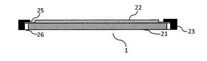
液晶表示ユニットは液晶表示セル、液晶表示セル上に配置された偏光板及び偏光板を取り囲む前記液晶表示セルを被膜する封止体を備え、
前記液晶表示ユニット又は前記保護板の少なくとも一方に、未硬化時に流動性を有する第2硬化性樹脂組成物を塗布し、前記第2硬化性樹脂組成物によって第1硬化性樹脂組成物の塗布領域を画定する第2硬化性樹脂組成物塗布工程と、
前記塗布領域又は前記塗布領域が形成された一方の基板と貼合わせる他方の基板における貼合わせた際に前記塗布領域と向かい合う領域に、未硬化時に流動性を有する前記第1硬化性樹脂組成物を塗布する第1硬化性樹脂組成物の塗布工程と、
前記第1硬化性樹脂組成物を介して前記液晶表示ユニットおよび前記保護板を貼合わせる貼合わせ工程と、
前記第1硬化性樹脂組成物を硬化させて前記液晶表示ユニットおよび前記保護板を貼合わせる第1硬化性樹脂組成物硬化工程と、を含み、
前記第2硬化性樹脂組成物を硬化して得られる硬化物層が、前記封止体の投影領域に積層され、かつ前記偏光板の投影領域には積層されていないことを特徴とする画像表示装置の製造方法。
(2)前記(1)に記載の画像表示装置の製造方法であって、
前記液晶表示ユニットの前記封止体表面上に前記第2硬化性樹脂組成物を塗布して硬化又は未硬化の塗布膜を形成し、
前記保護板の表面上に前記第1硬化性樹脂組成物を塗布して硬化又は未硬化の塗布膜を形成し、
前記塗布膜が形成された液晶表示ユニットと前記塗布膜が形成された保護板を貼合わせることを特徴とする(1)に記載の画像表示装置の製造方法。
(3)前記(1)又は(2)に記載の画像表示装置の製造方法であって、
前記第1硬化性樹脂組成物の塗布膜の平均厚みが、前記第2硬化性樹脂組成物の塗布膜の平均厚み以下であることを特徴とする(1)又は(2)に記載の画像表示装置の製造方法。
(4)前記(1)〜(3)のいずれか一項に記載の画像表示装置の製造方法であって、前記第2硬化性樹脂組成物を硬化して得られる第2硬化物層の塗膜幅の中間地点が、前記液晶表示セルの投影領域に存在しておらず、前記液晶表示セルを取り囲んで存在している別の光学部材の投影領域上に存在していることを特徴とする前記(1)〜(3)のいずれか一項に記載の画像表示装置の製造方法。
(5)(1)〜(4)のいずれか一項に記載の光学部材の製造方法の、前記第1硬化性樹脂組成物又は前記第2硬化性樹脂組成物用の、(メタ)アクリレート(A)及び光重合開始剤(B)を含有する硬化性樹脂組成物。
(6)(メタ)アクリレート(A)が、ウレタン(メタ)アクリレート、ポリイソプレン骨格を有する(メタ)アクリレート、ポリブタジエン骨格を有する(メタ)アクリレート、(メタ)アクリレートモノマーからなる群から選ばれる1種以上の(メタ)アクリレートである(5)に記載の硬化性樹脂組成物。
(7)アセトニトリル又はメタノール中で測定した光重合開始剤(B)のモル吸光係数が、302nm又は313nmでは300ml/(g・cm)以上であり、365nmでは100ml/(g・cm)以下である(5)又は(6)に記載の硬化性樹脂組成物。
(8)前記保護板が、遮光部を有する透明ガラス基板、遮光部を有する透明樹脂基板、遮光部と透明電極が形成されたガラス基板、遮光部を有する透明基板に透明電極が形成されたガラス基板またはフィルムが貼りあわされた基板の群から選ばれる1種以上からなる(5)〜(7)のいずれか一項に記載の硬化性樹脂組成物。
(9)前記第1硬化性樹脂組成物が紫外線を照射した際の硬化率80%における樹脂層の25℃における貯蔵剛性率に対して、紫外線を照射した際の硬化率98%における樹脂層の貯蔵剛性率が3〜20倍であることを特徴とする樹脂組成物であって、硬化率80%における貯蔵剛性率(25℃)が1×10²Pa〜1×10⁵Paである(5)〜(8)のいずれか一項に記載の硬化性樹脂組成物。
(10)(メタ)アクリレート(A)が、ウレタン(メタ)アクリレート、ポリイソプレン骨格を有する(メタ)アクリレート、ポリブタジエン骨格を有する(メタ)アクリレート、(メタ)アクリレートモノマーからなる群から選ばれる1種以上の(メタ)アクリレートである(5)〜(9)のいずれか一項に記載の硬化性樹脂組成物。
(11)前記保護板が、タッチパネルである(5)〜(10)のいずれか一項に記載の硬化性樹脂組成物。
(12)前記(1)〜(11)のいずれか一項に記載の画像表示装置の製造方法によって得られるタッチパネル。
(13)液晶表示ユニットに保護板を接着した画像表示装置であって、
液晶表示ユニットは液晶表示セル、液晶表示セル上に配置された偏光板及び偏光板を取り囲む前記液晶表示セルを被膜する封止体を備え、
前記偏光板上に形成された第1硬化性樹脂組成物を硬化して得られる第1硬化物層と、
前記第1硬化物層の周壁部を画成する第2硬化性樹脂組成物を硬化して得られる第2硬化物層を有し、
前記第2硬化物層が、前記封止体の投影領域に積層され、かつ前記偏光板の投影領域には積層されていないことを特徴とする画像表示装置。
(14)前記第1硬化性樹脂組成物及び前記第2硬化性樹脂組成物が、ウレタン(メタ)アクリレート化合物、ポリイソプレン骨格を有する(メタ)アクリレート化合物又はポリブタジエン骨格を有する(メタ)アクリレート化合物からなる群から選択される少なくとも1種の(メタ)アクリレート化合物、及び光重合開始剤を含有している硬化性樹脂組成物である、前記(13)に記載の画像表示装置。
(1) A method of manufacturing an image display device in which a protective plate is bonded to a liquid crystal display unit,
The liquid crystal display unit includes a liquid crystal display cell, a polarizing plate disposed on the liquid crystal display cell, and a sealing body that coats the liquid crystal display cell surrounding the polarizing plate,
A second curable resin composition having fluidity when uncured is applied to at least one of the liquid crystal display unit or the protective plate, and the application region of the first curable resin composition is applied by the second curable resin composition. A second curable resin composition application step that defines:
The first curable resin composition having fluidity when uncured is applied to a region facing the application region when the application region or one substrate on which the application region is formed is bonded to the other substrate. An application step of applying the first curable resin composition;
A laminating step of laminating the liquid crystal display unit and the protective plate via the first curable resin composition;
A first curable resin composition curing step for curing the first curable resin composition and bonding the liquid crystal display unit and the protective plate together,
An image display, wherein a cured product layer obtained by curing the second curable resin composition is laminated in a projection region of the sealing body and is not laminated in a projection region of the polarizing plate. Device manufacturing method.
(2) The method for manufacturing the image display device according to (1),
Applying the second curable resin composition on the surface of the sealing body of the liquid crystal display unit to form a cured or uncured coating film;
Applying the first curable resin composition on the surface of the protective plate to form a cured or uncured coating film,
The method for manufacturing an image display device according to (1), wherein the liquid crystal display unit on which the coating film is formed and the protective plate on which the coating film is formed are bonded together.
(3) The method for manufacturing the image display device according to (1) or (2),
The average thickness of the coating film of said 1st curable resin composition is below the average thickness of the coating film of said 2nd curable resin composition, The image display as described in (1) or (2) characterized by the above-mentioned. Device manufacturing method.
(4) The method for producing an image display device according to any one of (1) to (3), wherein the second cured product layer is obtained by curing the second curable resin composition. An intermediate point of the film width does not exist in the projection area of the liquid crystal display cell but exists on the projection area of another optical member that surrounds the liquid crystal display cell. The manufacturing method of the image display apparatus as described in any one of said (1)-(3).
(5) (meth) acrylate for the first curable resin composition or the second curable resin composition of the method for producing an optical member according to any one of (1) to (4) ( A curable resin composition containing A) and a photopolymerization initiator (B).
(6) One kind selected from the group consisting of (meth) acrylate (A), urethane (meth) acrylate, (meth) acrylate having a polyisoprene skeleton, (meth) acrylate having a polybutadiene skeleton, and (meth) acrylate monomer The curable resin composition according to (5), which is the above (meth) acrylate.
(7) The molar extinction coefficient of the photopolymerization initiator (B) measured in acetonitrile or methanol is 300 ml / (g · cm) or more at 302 nm or 313 nm, and is 100 ml / (g · cm) or less at 365 nm. The curable resin composition according to (5) or (6).
(8) The protective plate is a transparent glass substrate having a light shielding portion, a transparent resin substrate having a light shielding portion, a glass substrate having a light shielding portion and a transparent electrode formed thereon, and a glass having a transparent electrode formed on the transparent substrate having the light shielding portion. Curable resin composition as described in any one of (5)-(7) which consists of 1 or more types chosen from the group of the board | substrate or the board | substrate with which the film was pasted together.
(9) With respect to the storage rigidity at 25 ° C. of the resin layer at a curing rate of 80% when the first curable resin composition is irradiated with ultraviolet rays, the resin layer at a curing rate of 98% when irradiated with ultraviolet rays is used. The resin composition is characterized in that the storage rigidity is 3 to 20 times, and the storage rigidity (25 ° C.) at a curing rate of 80% is 1 × 10 2 Pa to 1 × 10 5 Pa (5 The curable resin composition according to any one of (8) to (8).
(10) One selected from the group consisting of (meth) acrylate (A), urethane (meth) acrylate, (meth) acrylate having a polyisoprene skeleton, (meth) acrylate having a polybutadiene skeleton, and (meth) acrylate monomer The curable resin composition according to any one of (5) to (9), which is the above (meth) acrylate.
(11) The curable resin composition according to any one of (5) to (10), wherein the protective plate is a touch panel.
(12) A touch panel obtained by the method for manufacturing an image display device according to any one of (1) to (11).
(13) An image display device in which a protective plate is bonded to a liquid crystal display unit,
The liquid crystal display unit includes a liquid crystal display cell, a polarizing plate disposed on the liquid crystal display cell, and a sealing body that coats the liquid crystal display cell surrounding the polarizing plate,
A first cured product layer obtained by curing the first curable resin composition formed on the polarizing plate;
A second cured product layer obtained by curing a second curable resin composition that defines a peripheral wall portion of the first cured product layer;
The image display apparatus, wherein the second cured product layer is laminated in a projection region of the sealing body and is not laminated in a projection region of the polarizing plate.
(14) The first curable resin composition and the second curable resin composition are a urethane (meth) acrylate compound, a (meth) acrylate compound having a polyisoprene skeleton, or a (meth) acrylate compound having a polybutadiene skeleton. The image display device according to (13), which is a curable resin composition containing at least one (meth) acrylate compound selected from the group consisting of: and a photopolymerization initiator.
本発明は液晶表示ユニットに保護板を接着した画像表示装置の製造方法であって、液晶表示ユニットは液晶表示セル、液晶表示セル上に配置された偏光板及び偏光板を取り囲む前記液晶表示セルを被膜する封止体を備える画像表示装置の製造方法及び画像表示装置に関し、当該画像表示装置の製造方法においては、下記[工程A]〜[工程D]により、画像表示装置を製造する。そして、後述する第2硬化性樹脂組成物を硬化して得られる第2硬化物層が、前記封止体の投影領域に積層され、かつ前記偏光板の投影領域には積層されていないことを特徴としている。ここで、工程Bにおける前記塗布領域が形成された一方の基板と貼合わせる他方の基板における貼合わせた際に前記塗布領域と向かい合う領域とは、即ち、2以上の基板を貼り合わせ際に第2硬化物層と各々の基材で規定される第1硬化物層が存在する第1硬化物層充填室において、塗布領域が形成された一方の基板と貼合わせる別の基板上における前記充填室を規定することとなる領域を示す。
[工程A]前記液晶表示ユニット又は前記保護板の少なくとも一方に、未硬化時に流動性を有する第2硬化性樹脂組成物を塗布し、前記第2硬化性樹脂組成物によって第1硬化性樹脂組成物の塗布領域を画定する第2硬化性樹脂組成物塗布工程。
[工程B]前記塗布領域又は前記塗布領域が形成された一方の基板と貼合わせる他方の基板における貼合わせた際に前記塗布領域と向かい合う領域に、未硬化時に流動性を有する前記第1硬化性樹脂組成物を塗布する第1硬化性樹脂組成物の塗布工程。
[工程C]前記第1硬化性樹脂組成物を介して前記液晶表示ユニットおよび前記保護板を貼合わせる貼合わせ工程。
[工程D]前記第1硬化性樹脂組成物を硬化させて前記液晶表示ユニットおよび前記保護板を貼合わせる第1硬化性樹脂組成物硬化工程。
以下、本発明の製造方法、及びこの方法により製造した画像表示装置の形態について、図面を参照しつつ説明する。尚、第1〜第3の実施形態は具体例であり、これらの具体例に限定されるものではない。
The present invention relates to a method of manufacturing an image display device in which a protective plate is bonded to a liquid crystal display unit, the liquid crystal display unit including a liquid crystal display cell, a polarizing plate disposed on the liquid crystal display cell, and the liquid crystal display cell surrounding the polarizing plate. In regard to a method for manufacturing an image display device including an encapsulating sealing body and an image display device, the image display device is manufactured by the following [Step A] to [Step D]. And the 2nd hardened material layer obtained by hardening the 2nd curable resin composition mentioned below is laminated on the projection field of the encapsulant, and is not laminated on the projection field of the polarizing plate. It is a feature. Here, the area facing the application area when bonded on the other substrate to be bonded to the one substrate on which the application area is formed in Step B is the second area when two or more substrates are bonded. In the first cured product layer filling chamber in which the cured product layer and the first cured product layer defined by each base material exist, the filling chamber on another substrate to be bonded to one substrate on which the application region is formed is provided. Indicates the area to be defined.
[Step A] A second curable resin composition having fluidity when uncured is applied to at least one of the liquid crystal display unit or the protective plate, and the first curable resin composition is formed by the second curable resin composition. 2nd curable resin composition application | coating process which demarcates the application | coating area | region of a thing.
[Step B] The first curability having fluidity when uncured in an area facing the application area when the application area or the other substrate on which the application area is formed is bonded to the other substrate. The application | coating process of the 1st curable resin composition which apply | coats a resin composition.
[Step C] A laminating step of laminating the liquid crystal display unit and the protective plate via the first curable resin composition.
[Step D] A first curable resin composition curing step in which the first curable resin composition is cured and the liquid crystal display unit and the protective plate are bonded together.
Hereinafter, the manufacturing method of the present invention and the form of an image display device manufactured by this method will be described with reference to the drawings. The first to third embodiments are specific examples and are not limited to these specific examples.
(第1の実施形態)
図1は、本発明の光学部材の製造工程の第1の実施形態を示す工程図である。
この方法は、液晶表示ユニット1と保護板2を貼り合わせることにより光学部材(画像表示装置)を得る方法である。
(First embodiment)
FIG. 1 is a process diagram showing a first embodiment of a manufacturing process of an optical member of the present invention.
This method is a method of obtaining an optical member (image display device) by bonding the liquid
液晶表示ユニット1は、電極を形成した一対の基板間に液晶材料が封入されたものに偏光板、駆動用回路、信号入力ケーブル、バックライトユニットが備わったものを言う。
図2は、液晶表示ユニット1の一例の要部を示す断面図である。この液晶表示ユニット1では、図2に示すように、液晶表示セル21上に偏光板22が配置され、液晶表示セル21上に偏光板22を取り囲むように封止体23を配置した構成となっている。ここで、液晶表示セル21上に偏光板22が直接積層された構造について示されているが、直接積層させる必要はなく、液晶表示セルの上に偏光板が配置されていればよく、液晶表示セルと偏光板との間に別の機能性フィルム等の光学部材を介在させても構わない。
この状態では、偏光板22と封止体23の間には最大幅数mmの隙間24が形成されており、隙間24の底面には、液晶表示セル21の表面が露出しないように密閉フィルム25が配置されている例を示している。即ち、図2の例に示すように、偏光板22上に第2硬化性樹脂組成物11を塗布する前に、偏光板22と封止体23との間の隙間24の底面である液晶表示セル21の表面上に、接着性を有する密閉フィルム25を配置し、隙間24の一部を閉塞することができる。密閉フィルム25の幅方向の一端は偏光板24に隣接し、他端は封止体23に密着するため、隙間24の底部が密閉される。ここで、図2においては、密閉フィルム25を配置している例を示したが、隙間24の底面において密閉フィルム25が配置されず、液晶表示セル21の表面が露出していても構わない。
このような密閉フィルム25としては、ポリエチレンテレフタレート等をフィルム基材とし、アクリレート等の粘着剤層あるいは接着剤層を有する粘着フィルムが好ましい。
上記偏光板22としては、画像表示装置に使用される公知のものを使用できるが、例えばフィルム状の吸収型偏光子、ワイヤグリッド型偏光子等が使用できる。
The liquid
FIG. 2 is a cross-sectional view showing a main part of an example of the liquid
In this state, a gap 24 having a maximum width of several mm is formed between the
As such a
As the
なお、密閉フィルム25は、配置時に必ずしも粘着剤層あるいは接着剤総は固体である必要はなく、液晶表示ユニットの各構成部材間の間隙に侵入しない程度に高粘度であればよい。より具体的には粘度65Pa・s程度の硬化性樹脂組成物を使用することができる。また、隙間に入り込まない程度に形状を保持させる点から、チキソ比3程度の接着剤を使用してもよい。
In addition, the sealing
液晶表示セル21には偏光板22が形成された面とは反対側の面に、バックライト側偏光板27を積層させることができる。ここで、液晶表示セル21にバックライト側偏光板27が直接積層された構造に限らず、液晶表示セル21に偏光板22が配置されていればよく、液晶表示セル21とバックライト側偏光板27との間に別の機能性フィルム等の光学部材を介在させても構わない。
さらに、バックライト側偏光板27において、液晶表示セル21が配置されている面とは反対側の面にバックライト28を形成することができる。バックライトを構成する光源としては、例えば、冷陰極管やLED(Light Emitting Diode)等を用いることができる。具体例としては、光源30を導光板31の一端に配設し、光源30からの線状光を導光板31で面状光に変換するエッジライト方式を例示できる。なお、バックライト方式は、エッジライト方式に限定されるものではない。例えば、拡散板の直下に光源30を配置する直下型方式を採用してもよい。
A backlight side polarizing plate 27 can be laminated on the surface of the liquid
Further, in the backlight side polarizing plate 27, the backlight 28 can be formed on the surface opposite to the surface on which the liquid
液晶表示ユニット1を保護するため、液晶表示ユニット1は通常筐体26で覆われている。筐体26は、金属製の材料が使用されることが一般的であり、具体的には、ステンレス等の合金、鉄、アルミ、銀が使用されること可能である。
筐体26内には、液晶表示セル、バックライト、導光板、光学フィルムを収容することができる。
In order to protect the liquid
A liquid crystal display cell, a backlight, a light guide plate, and an optical film can be accommodated in the
液晶表示ユニット1においては、液晶表示セル21を被膜するように封止体23が配置されている。図2においては、偏光フィルム22の周壁部に隙間24を介在した状態で偏光フィルムを囲い込んで封止体23が配置されている。また、図2においては、液晶表示セル21上に密閉フィルム25を介在させて封止体23を被膜しているが、液晶表示セル21に直接被膜しても構わない。
封止体23は、画像表示装置の外壁を被膜しており、図2においては液晶表示セル21の周壁部に隣接して配置されている筐体26を直接被膜している例であるが、特に当該態様に限定して配置される必要はない。尚、図示していないが、前記の通り液晶表示セル21の偏光板22が形成された面とは反対側の面に、バックライト側偏光板27を積層させ、さらにバックライト側偏光板27にバックライト28が積層され、バックライト28を筐体26が隣接して覆っており、当該筐体26がこれらの部材の周壁部を覆う態様で配置することができる。そして、筐体26をさらに封止体23が被膜している構成とすることができる。
封止体23としては、有機高分子材料が使用されることが一般的であり、具体的には、PET等のフィルム基材に、アクリルポリマー系等の粘着層又は接着層を有する粘着フィルム等が使用できる。
In the liquid
The sealing
As the sealing
図3に示す保護板2は、前記液晶表示ユニット1を保護するものである。そして、保護板2は透明基板3と透明基板3の片面表面上に形成された遮光部4を有する部材である。
保護板2に使用する透明基板3としては、ガラス板、または透明樹脂板が挙げられ、表示パネルからの出射光や反射光に対して透明性が高い点はもちろん、耐光性、低複屈折率、高い平面精度、耐表面傷付性、および高い機械的強度を有する点から、ガラス板が好ましい。
A
Examples of the
ガラス板の材料としては、ソーダイムガラス等のガラス材料が挙げられ、鉄分より低く、青みの少ない高透過ガラスがより好ましい。安全性を高めるために表面材として強化ガラスを用いても良い。特に薄いガラス板を用いる場合には、化学強化を施したガラス板を用いることが好ましい。
透明樹脂板の材料としては、ポリメチルメタクリレート(PMMA)板、ポリカーボネート(PC)板、脂環式ポリオレフィンポリマー(COP)板等の透明性の高い樹脂材料が挙げられる。
Examples of the material for the glass plate include glass materials such as sodaime glass, and a high transmission glass that is lower than iron and less bluish is more preferable. In order to improve safety, tempered glass may be used as a surface material. In particular, when a thin glass plate is used, it is preferable to use a chemically strengthened glass plate.
Examples of the material for the transparent resin plate include highly transparent resin materials such as a polymethyl methacrylate (PMMA) plate, a polycarbonate (PC) plate, and an alicyclic polyolefin polymer (COP) plate.
保護板2には、樹脂硬化物層との界面接着力を向上させるために、表面処理を施してもよい。表面処理の方法としては、保護板2の表面をシランカップリング剤で処理する方法、フレームバーナーによる酸化炎によって酸化ケイ素の薄膜を形成する方法等が挙げられる。
The
保護板2には、表示画像のコントラストを高めるために、後述する第1硬化性樹脂組成物を硬化して得られる第2硬化物層14ないし第2硬化性樹脂組成物14を硬化して得られる第1硬化物層13が形成された側に対して反対側の表面に反射防止層を設けてもよい。反射防止層は、保護板2の表面に無機薄膜を直接形成する方法、または反射防止層を設けた透明樹脂フィルムを保護板2に貼合する方法によって設けることができる。
The
また、目的に応じて、保護板2の一部または全体を着色したり、保護板2の表面の一部または全体を磨りガラス状にして光を散乱させたり、保護板2の表面の一部または全体に微細な凹凸等を形成して透過光を屈折または反射させたりしてもよい。また、着色フィルム、光散乱フィルム、光屈折フィルム、光反射フィルム等を、保護板2の表面の一部または全体に貼着してもよい。
Further, depending on the purpose, a part or the whole of the
保護板2の形状は、通常矩形である。
保護板2の大きさは、本発明の製造方法が比較的大面積の画像表示装置の製造に特に適していることから、テレビ受像機の場合、0.5m×0.4m以上が適当であり、0.7m×0.4m以上が特に好ましい。保護板2の大きさの上限は、表示パネルの大きさで決まることが多い。また、あまりに大きい画像表示装置は、設置等における取り扱いが困難となりやすい。保護板2の大きさの上限は、これらの制約から、通常2.5m×1.5m程度である。
The shape of the
The size of the
保護板2の厚さは、機械的強度、透明性等の点から、ガラス板の場合は通常0.5〜25mmである。屋内で使用するテレビ受像機、PC用ディスプレイ等の用途では、表示装置の軽量化の点から、1〜6mmが好ましく、屋外に設置する公衆表示用途では、3〜20mmが好ましい。化学強化ガラスを用いる場合は、ガラスの厚さは、強度の点で、0.5〜1.5mm程度が好ましい。透明樹脂板の場合は、2〜10mmが好ましい。
The thickness of the
遮光部4は、後述する液晶表示セルの画像表示領域以外が保護板2側から視認できないようにして、表示パネルに接続されている配線部材等を隠蔽するものである。遮光部4は、後述する第2硬化物層14ないし第1硬化物層13が形成される側の表面に形成することができ、遮光部4と画像表示領域との視差を低減する。保護板2がガラス板の場合、遮光印刷部に黒色顔料を含むセラミック印刷を用いると遮光性が高く好ましい。保護板2に貼合される面に遮光部4を設け、その裏面、すなわち表示装置の最表面に反射防止層を設けたフィルムを保護板に貼合してもよい。例えば、遮光部4はテープの貼付や塗料の塗布又は印刷等によって形成されている。
尚、本発明においては遮光部4を有さないものにも適用できるが、以下の第1〜3の実施形態の説明では、遮光部4を備える場合を具体例として説明を行う。
The light-shielding
In the present invention, the present invention can also be applied to a device that does not have the
[工程A]
図1(a)に示すように、後述する(メタ)アクリレート(A)および光重合開始剤(B)を含む第2硬化性樹脂組成物12を、液晶表示ユニット1の前記封止体23の表面に塗布する。ここで、具体例として封止体23の表面に塗布する例を示したが、第2硬化性樹脂組成物12は封止体23の投影領域に塗布すればよく、第2硬化性樹脂組成物12と封止体23の間に別の光学部材が介在しても構わない。塗布の方法としては、ディスペンス方式、スクリーン印刷法等が挙げられる。ここで、第2硬化性樹脂組成物12は、貼合わせ時に後述する第1硬化性樹脂組成物の堰部となるため、第1硬化性樹脂組成物11を硬化して得られる第1硬化物層13を画成したい形状に塗布する。具体的には、正方形ないし長方形等の枠の形状にすることができるが、形状は特に限定されない。このようにして、貼合わせた際に第1硬化物層13が充填される充填室を規定する層が形成される。
ここで、液晶表示ユニット1と保護板2の表面に塗布する第1硬化性樹脂組成物及び第2硬化性樹脂組成物は同一であってもよいし、異なる硬化性樹脂組成物を用いても構わない。
また、液晶表示ユニット1と保護板2との間隔を保持するために、第2硬化性樹脂組成物12に所定の粒子径のスペーサー粒子を配合してもよい。
[Step A]
As shown to Fig.1 (a), the 2nd
Here, the first curable resin composition and the second curable resin composition applied to the surfaces of the liquid
Moreover, in order to maintain the space | interval of the liquid
ここで、本発明において、第2硬化性樹脂組成物12は、前記封止体の投影領域に積層され、かつ前記偏光板の投影領域には積層されない。このように偏光板の投影領域を避け、封止体の投影領域に第2硬化性樹脂組成物12を塗布することで、第2硬化性樹脂組成物12を硬化して得られる第2硬化物層が封止体23上に形成される。当該箇所に第2硬化物層を積層させることにより、指等による押圧により第2硬化物層13上に圧力をかけても、画像表示部に波紋が生じることを防止することができる。一方、第2硬化物層12が偏光板上に積層されると、第2硬化物層上ないし画像表示領域の周壁部に圧力を加えると、干渉により波紋が生じることとなる。
さらに、第2硬化物層の塗膜幅の中間地点が、前記液晶表示セルの投影領域に存在していないように配置し、隙間24の投影領域上ではなく前記液晶表示セル21を取り囲んで存在している別の光学部材の投影領域上に配置することにより、押圧により液晶表示セル上に加わる圧力が低減されるため、圧力を加えても液晶表示セルの画像表示を乱すことが低減され、より波紋が生じることを防ぐことが可能となる。
Here, in this invention, the 2nd
Further, the intermediate point of the coating film width of the second cured product layer is arranged so as not to exist in the projection area of the liquid crystal display cell, and surrounds the liquid
液晶表示ユニット1の画像表示領域の外側の領域が比較的狭いため、塗布膜を形成する第2硬化性樹脂組成物12による塗布膜の幅は狭くすることが好ましい。当該幅は、0.5〜3mmが好ましく、0.5〜1.6mmがより好まく、0.5〜1.0mmがさらに好ましい。また、形成される第1硬化性樹脂組成物11の塗布膜の厚さは、形成される第2硬化性樹脂組成物12の塗布膜の平均的な厚みとほぼ等しいか、または形成される第1硬化性樹脂組成物11が、形成される第2硬化性樹脂組成物12の厚みより0.005〜1mm厚いことが好ましく、0.01〜0.08mm厚いことがより好ましく、0.01〜0.05mm厚いことがより好ましい。
第2硬化性樹脂組成物12における硬化時の25℃における貯蔵剛性率は、第1硬化性樹脂組成物11の硬化物層の25℃における貯蔵剛性率よりも大きいことが好ましい。第2硬化物層14の貯蔵剛性率が、第1硬化性樹脂組成物を硬化して得られる第1硬化物層13の貯蔵剛性率よりも大きければ、液晶表示ユニット1と保護板2とを貼合する際に、第1硬化物層13の周縁部において、保護板2と第1硬化物層13との界面に空隙が残存していても、空隙が外部に開放されにくく、独立した空隙となりやすい。よって、減圧雰囲気下にて液晶表示ユニット1と保護板2とを貼合した後、これを大気圧雰囲気下に戻した際に、空隙内の圧力(減圧のまま)と樹脂硬化物層15にかかる圧力(大気圧)との差圧によって空隙の体積が減少し、空隙は消失しやすい。
Since the area outside the image display area of the liquid
The storage rigidity at 25 ° C. at the time of curing in the second
第2硬化性樹脂組成物12の硬化時の収縮率が、第1硬化性樹脂組成物11の硬化時の収縮率より大きくなるように、第2硬化性樹脂組成物12および第1硬化性樹脂組成物11を設計することが好ましい。第1硬化性樹脂組成物11を硬化してなる第1硬化物層13には、硬化時の収縮率に応じた収縮応力が第1硬化物層13の厚さ方向に残留していると考えられ、硬化時において層状部に残留する厚さ方向の収縮応力により第1硬化物層13の厚さがわずかに減少する。第2硬化性樹脂組成物12より硬化時の収縮率の小さい第1硬化性樹脂組成物11を用いることで、表示領域内における応力を緩和し、表示ムラの発生を抑制する事が出来る。
The second
第2硬化性樹脂組成物12の硬化時の収縮率を第1硬化性樹脂組成物11の硬化時の収縮率より大きくする手段のひとつは、第2硬化性樹脂組成物12の硬化性基の数を第1硬化性樹脂組成物11の硬化性基の数より多くすることである。そのためには、第2硬化性樹脂組成物12において(i)分子量の小さい硬化性化合物(モノマー)の含有量を多くしたり、(ii)反応基を分子中に複数有する多官能成分の含有量を多くしたりすればよい。
すなわち、第2硬化性樹脂組成物12の粘度を、第1硬化性樹脂組成物11の粘度より高くすればよい。具体的には、第2硬化性樹脂組成物12の未硬化時の粘度は、第1硬化性樹脂組成物11の未硬化時の粘度の2倍以上が好ましく、5倍以上がより好ましく、10倍以上がさらに好ましい。また、第2硬化性樹脂組成物12を塗布により透明面材上に形成するためには、第2硬化性樹脂組成物12の25℃における未硬化時の粘度は、3000Pa・s以下であることが好ましい。
ここで、第2硬化性樹脂組成物12の好適な粘度は具体的には、40〜70Pa・sである。40Pa・s未満であると第2硬化性樹脂組成物12が形状を保持できず広がってしまい、厚みの制御が困難となる上、第2硬化性樹脂樹脂組成物12が第2硬化性樹脂組成物12を決壊させてしまう恐れがある。一方、粘度が70Pa・sを超える場合には、塗布器から吐出させることが困難となる恐れがある。
One of means for increasing the shrinkage rate at the time of curing of the second
That is, the viscosity of the second
Here, the suitable viscosity of the 2nd
また、第2硬化物層14には、第2硬化物層14と液晶表示ユニット1との界面、および第2硬化物層14と保護板2との界面から液状の第1硬化性樹脂組成物11が漏れ出さない程度以上の界面密着力、および形状を維持できる程度の固さが必要である。よって、第2硬化物層14には、粘度の高い第2硬化性樹脂組成物12を用いることが好ましい。
Further, the second cured
第2硬化性樹脂組成物12は、光硬化性樹脂組成物であってもよく、熱硬化性樹脂組成物であってもよい。第2硬化性樹脂組成物12としては、低温で硬化でき、かつ硬化速度が速い点から、硬化性化合物および光重合開始剤を含む光硬化性樹脂組成物が好ましい。
The second
上記の通り形成した第2硬化性樹脂組成物12をそのまま塗布膜として堰部を形成することとし、次の工程Bに適用することが可能であるが、当該第2硬化性樹脂組成物12を仮硬化させて硬化塗布膜を得ることで堰部を形成することも可能である。
硬化させる場合においては、塗布後の第2硬化性樹脂組成物12に紫外線5を照射して、塗布層の下部側(硬化性樹脂組成物からみて液晶表示ユニット側)に存在する硬化部分(図では未表示)と塗布層の上部側(液晶表示ユニット側と反対側)(大気中で行うときは大気側)に存在する未硬化部分(図では未表示)を有する第2硬化物層14を得る。照射量は5〜2000mJ/cm2が好ましく、特に好ましくは、10〜1000mJ/cm2、特に好ましくは10〜500mJ/cm2である。照射量が少なすぎると、最終的に貼り合せた光学部材の樹脂の硬化度が不十分となるおそれがあり、照射量が多すぎると未硬化成分が少なくなり、液晶表示ユニット1と保護板2の貼り合せが不良となる恐れがある。
本発明において、「未硬化」とは25℃環境下で流動性がある状態を示すものとする。また、紫外線照射後に樹脂組成物層を指で触り、指に液状成分が付着する場合は、未硬化部分を有するものと判断される。
紫外〜近紫外の紫外線照射による硬化には、紫外〜近紫外の光線を照射するランプであれば光源を問わない。例えば、低圧、高圧若しくは超高圧水銀灯、メタルハライドランプ、(パルス)キセノンランプ、LEDランプまたは無電極ランプ等が挙げられる。
It is possible to apply the second
In the case of curing, the second
In the present invention, “uncured” refers to a fluid state in a 25 ° C. environment. In addition, when the resin composition layer is touched with a finger after ultraviolet irradiation and a liquid component adheres to the finger, it is determined to have an uncured portion.
For curing by ultraviolet irradiation from ultraviolet to near ultraviolet, any light source may be used as long as it is a lamp that irradiates ultraviolet to near ultraviolet rays. For example, a low-pressure, high-pressure or ultrahigh-pressure mercury lamp, metal halide lamp, (pulse) xenon lamp, LED lamp or electrodeless lamp can be used.
[工程B]
次に、図1(b)に示すように、後述する(メタ)アクリレート(A)および光重合開始剤(B)を含む第1硬化性樹脂組成物11を、遮光部4を有する保護板2の遮光部4が形成されている面の表面に塗布する。塗布の方法としては、スリットコーター、ロールコーター、スピンコーター、スクリーン印刷法等が挙げられる。
得られる塗布膜としては、工程Aで形成された第2硬化物層で形成された枠内となるように形成されることが好ましい。枠外の箇所があると、液晶表示ユニット1と保護板2を貼合わせた際に第1硬化性樹脂組成物11が押されてしまい不具合が生じる恐れがあるためである。ここで、第1硬化性樹脂組成物11の塗布膜は第2硬化物層14に必ずしも厳密に沿って形成される必要はなく、第2硬化物層14で形成された枠内に収まっており、画像表示装置の視認領域を充填するように形成されていればよい。また、第1硬化性樹脂組成物11は上記領域に塗布すればよく、第1硬化性樹脂組成物11と塗布する基板との間に別の光学部材が介在しても構わない。
第1硬化性樹脂組成物11は、前記塗布領域又は前記塗布領域が形成された一方の基板と貼合わせる他方の基板における貼合わせた際に前記塗布領域と向かい合う領域に塗布される。こうして、貼合わせた際に前記充填室を規定する領域となる第2硬化性樹脂組成物12が塗布された一方の基板上又は貼り合わせる他方の基板上の領域に第1硬化性樹脂組成物11が塗布されることとなる。
[Step B]
Next, as shown in FIG.1 (b), the
The obtained coating film is preferably formed so as to be within the frame formed by the second cured product layer formed in step A. This is because if there is a part outside the frame, the first
The 1st
第1硬化性樹脂組成物11において、第1硬化性樹脂組成物11を硬化して得られる第1硬化物層の25℃における貯蔵剛性率は、102〜107Paが好ましく、102〜105Paがより好ましい。更に、貼合時の空隙をより短時間に消失させるためには、102〜104Paが特に好ましい。貯蔵剛性率が103Pa以上であれば、第1硬化物層13の形状を維持しやすい。また、形成される第1硬化性樹脂組成物11の厚さが比較的厚い場合であっても、第1硬化物層13全体で厚さを均一に維持でき、保護板2と液晶表示ユニット1とを貼合する際に、液晶表示ユニット1と第1硬化物層13との界面に空隙が発生しにくい。貯蔵剛性率が107Pa以下であれば、良好な密着性を発揮できる。また、形成する樹脂材の分子運動性が比較的高いため、減圧雰囲気下にて液晶表示ユニット1と保護板2とを貼合した後、これを大気圧雰囲気下に戻した際に、空隙内の圧力(減圧のまま)とフィル材硬化物層にかかる圧力(大気圧)との差圧によって空隙の体積が減少しやすくなり、また、体積が減少した空隙内の気体がフィル材硬化物層に溶解し、吸収されやすい。
In the first
第1硬化性樹脂組成物11の厚さは、50〜500μmが好ましく、50〜350μmがより好ましく、100〜350μmが特に好ましい。第1硬化性樹脂組成物11の厚さが50μm以上であれば、保護板2側からの外力による衝撃等を第1硬化物層13が効果的に緩衝して、液晶表示ユニット1を保護できる。また、本発明の画像表示装置の製造方法において、液晶表示ユニット1と保護板2との間に第1硬化物層13の厚さを超えない異物が混入しても、第1硬化物層13の厚さが大きく変化することなく、光透過性能への影響が少ない。第1硬化物層13の厚さが500μm以下であれば、第1硬化物層13に空隙が残留しにくく、また、画像表示装置の全体の厚さが不要に厚くならない。
第1硬化物層13の厚さを調整する方法としては、第2硬化物層14の厚さを調節するとともに、保護板2の表面に供給される液状の第2硬化性樹脂組成物11の供給量を調節する方法が挙げられる。
The thickness of the first
As a method of adjusting the thickness of the first cured
第1硬化性樹脂組成物11の粘度は、0.05〜50Pa・sが好ましく、1〜20Pa・sがより好ましい。粘度が0.05Pa・s以上であれば、第1硬化物層13の物性の低下が抑えられる。また、低沸点の成分が少なくなるため、後述する減圧雰囲気下における揮発が抑えられ好適となる。粘度が50Pa・s以下であれば、第1硬化物層13に空隙が残留しにくい。
第1硬化性樹脂組成物11の粘度は、25℃においてE型粘度計を用いて測定する。
The viscosity of the first
The viscosity of the first
第1硬化性樹脂組成物11は、光硬化性樹脂組成物であってもよく、熱硬化性樹脂組成物であってもよい。第1硬化性樹脂組成物としては、低温で硬化でき、かつ硬化速度が速い点から、硬化性化合物および光重合開始剤を含む光硬化性樹脂組成物が好ましい。
The first
ここで、第1硬化性樹脂組成物11を未硬化のまま貼合わせに用いてもよいが、図1(b)に記載したように仮硬化させることが好ましい。
具体的には、塗布後の第1硬化性樹脂組成物11の塗布膜に紫外線5を照射して、塗布層の下部側(硬化性樹脂組成物からみて透明基板側)に存在する硬化部分(図では未表示)と塗布層の上部側(透明基板側と反対側)(大気中で行うときは大気側)に存在する未硬化部分(図では未表示)を有する硬化物層を得る。照射量は5〜2000mJ/cm2が好ましく、特に好ましくは、10〜1000mJ/cm2、特に好ましくは10〜500mJ/cm2である。照射量が少なすぎると、最終的に貼り合せた光学部材の樹脂の硬化度が不十分となるおそれがあり、照射量が多すぎると未硬化成分が少なくなり、液晶表示ユニット1と遮光部を有する透明基板2の貼り合せが不良となる恐れがある。
本発明において、「未硬化」とは25℃環境下で流動性がある状態を示すものとする。また、紫外線照射後に樹脂組成物層を指で触り、指に液状成分が付着する場合は、未硬化部分を有するものと判断される。
紫外〜近紫外の紫外線照射による硬化には、紫外〜近紫外の光線を照射するランプであれば光源を問わない。例えば、低圧、高圧若しくは超高圧水銀灯、メタルハライドランプ、(パルス)キセノンランプ、LEDランプまたは無電極ランプ等が挙げられる。
さらに好ましくは、本発明の工程1においては、硬化性樹脂組成物に照射される紫外線が、320nm〜450nmの範囲での最大照度を100とした時、200〜320nmにおける最大照度の比率(照度比)は30以下であり、特に好ましくは200〜320nmにおける照度が10以下である。320nm〜450nmの範囲での最大照度を100とした時、200〜320nmにおける最大照度の比率(照度比)は30よりも高いと、最終的に得られる光学部材の接着強度が劣ってしまう。これは、低波長での照度が高いと、工程1における硬化時に過度に硬化性樹脂組成物の硬化が進んでしまい、工程3における紫外線の照射における硬化の際の密着性に対する寄与が減少してしまうためと考えられる。尚、照度としては通常、各波長(例えば、365nm)で例えば30〜1000mW/cm2である。
ここで、上記照度比率となるように紫外線を照射する方法は、例えば、紫外〜近紫外の光線を照射するランプとして、当該照度比率の条件を満たすランプを適用する方法や、ランプ自体が当該照度の条件を満たさない場合であっても、工程1の照射時において短波長の紫外線をカットする基材(例えば、短波紫外線カットフィルター、ガラス板、フィルム等)を使用することで、このような照度比率で照射することが可能となる。紫外線の照度比率を調整する基材としては特には限定されないが、例えば、短波紫外線カット処理が施されたガラス板、ソーダ石灰ガラス、PETフィルム等が挙げられる。
この場合において、紫外線の照射は、通常大気中で、塗布側の上部側表面(硬化性樹脂組成物層から見て、透明基板側と反対側)(通常大気面)から照射するのが好ましい。また、真空にした後に硬化阻害性の気体を塗布層の上面表面に噴霧しながら紫外線の照射を行っても構わない。大気中で樹脂組成物を硬化した場合には、液晶表示ユニット側と反対側または透明基板側と反対側は大気側となる。
Here, the first
Specifically, the coating film of the first
In the present invention, “uncured” refers to a fluid state in a 25 ° C. environment. In addition, when the resin composition layer is touched with a finger after ultraviolet irradiation and a liquid component adheres to the finger, it is determined to have an uncured portion.
For curing by ultraviolet irradiation from ultraviolet to near ultraviolet, any light source may be used as long as it is a lamp that irradiates ultraviolet to near ultraviolet rays. For example, a low-pressure, high-pressure or ultrahigh-pressure mercury lamp, metal halide lamp, (pulse) xenon lamp, LED lamp or electrodeless lamp can be used.
More preferably, in
Here, the method of irradiating ultraviolet rays so as to achieve the above illuminance ratio is, for example, a method of applying a lamp satisfying the illuminance ratio as a lamp that irradiates ultraviolet to near-ultraviolet rays, or the lamp itself has the illuminance. Even if the above condition is not satisfied, such illuminance can be obtained by using a base material (for example, a short wave ultraviolet cut filter, a glass plate, a film, etc.) that cuts short wavelength ultraviolet rays at the time of irradiation in
In this case, it is preferable to irradiate the ultraviolet rays from the upper surface (on the side opposite to the transparent substrate as viewed from the curable resin composition layer) (normal air surface) on the coating side in normal air. Further, ultraviolet irradiation may be performed while spraying a curing-inhibiting gas on the upper surface of the coating layer after evacuation. When the resin composition is cured in the atmosphere, the side opposite to the liquid crystal display unit side or the side opposite to the transparent substrate side is the atmosphere side.
紫外線照射時に、紫外線硬化型樹脂層(塗布層)表面に酸素又はオゾンを吹きかけることにより、未硬化部分の状態や未硬化部分の膜厚を調整することができる。
即ち、塗布層の表面に酸素又はオゾンを吹きかけることにより、その表面において、硬化性樹脂組成物の硬化の酸素阻害が生じるため、その表面の未硬化部分を確実にしたり、また、未硬化部分の膜厚を厚くすることができる。
The state of the uncured portion and the film thickness of the uncured portion can be adjusted by spraying oxygen or ozone onto the surface of the ultraviolet curable resin layer (coating layer) during the ultraviolet irradiation.
That is, by spraying oxygen or ozone on the surface of the coating layer, oxygen inhibition of curing of the curable resin composition occurs on the surface, so that the uncured portion of the surface can be ensured, The film thickness can be increased.
ここで、本明細書において、硬化率とは硬化性樹脂組成物の硬化成分からみた硬化率を表しており、柔軟化剤等の硬化しない成分は除いて算出されるものを表す。尚、硬化率は本発明において、硬化収縮率は、25℃における硬化前の液比重と硬化して得られる25℃における膜比重から下記の数式(1)から算出できる
(数式1)
硬化収縮率=(膜比重−液比重)/膜比重×100 (1)
Here, in this specification, the curing rate represents the curing rate as seen from the curing component of the curable resin composition, and represents a value calculated by excluding components that are not cured such as a softening agent. The curing rate in the present invention can be calculated from the following formula (1) from the liquid specific gravity before curing at 25 ° C. and the film specific gravity at 25 ° C. obtained by curing (Formula 1).
Curing shrinkage = (film specific gravity−liquid specific gravity) / film specific gravity × 100 (1)
本発明の第1硬化性樹脂組成物11は、上記[工程B]において紫外線を照射した際の樹脂層の25℃における貯蔵剛性率に対して、上記[工程D]において紫外線を照射した際の樹脂層の貯蔵剛性率が3〜20倍(好ましくは、3〜10倍)であることを特徴とする樹脂組成物であることが好ましい。
貯蔵剛性率の測定方法としては、例えば下記の手法で測定することができる。具体的には、フッ素系離型剤を塗布した厚さ40μmのPETフィルム2枚を用意し、そのうちの1枚の離型剤塗布面に、得られた硬化性樹脂組成物を硬化後の膜厚が600μmとなるように塗布した。その後、2枚のPETフィルムを、それぞれの離型剤塗布面が互いに向かい合うように貼り合わせた。PETフィルム越しに高圧水銀灯(80W/cm、オゾンレス)で積算光量2000mJ/cm2の紫外線照射し、該樹脂組成物を硬化させた。その後、2枚のPETフィルムを剥離し、剛性率測定用の硬化物を作製する。そして、剛性率については、ARES(TA Instruments)を用いて、20〜40℃の温度領域において剛性率を測定できる。
[工程D]における本硬化時における硬化率は95%以上である。
The first
As a method for measuring the storage rigidity, for example, it can be measured by the following method. Specifically, two 40 μm-thick PET films coated with a fluorine-based mold release agent are prepared, and a film obtained by curing the obtained curable resin composition on one of the release agent-coated surfaces. It was applied so that the thickness was 600 μm. Thereafter, the two PET films were bonded together so that the respective release agent application surfaces face each other. The resin composition was cured by irradiating ultraviolet rays with an integrated light amount of 2000 mJ / cm 2 through a PET film with a high-pressure mercury lamp (80 W / cm, ozone-less). Thereafter, the two PET films are peeled off to produce a cured product for measuring the rigidity. And about a rigidity, a rigidity can be measured in the temperature range of 20-40 degreeC using ARES (TA Instruments).
The curing rate during the main curing in [Step D] is 95% or more.
本発明の第1硬化性樹脂組成物11は、前記仮硬化時に25℃における貯蔵剛性率が1×10²Pa〜1×10⁴Paであることが好ましい。
貯蔵剛性率が1×10⁴Paより大きいと第1硬化性樹脂組成物11は硬化により収縮するところ、収縮する力が生じることとなることから、第1硬化性樹脂組成物11が基材に追従せず、剥がれが生じたり、基材が歪んでしまったり、応力が十分に緩和されないことで、光学部材を得た際に表示ムラが生じることとなる。また、真空中での貼り合わせにおいては、仮硬化時の貯蔵剛性率が上記範囲にあることで、大気圧下に移動させた際に不具合を生じさせることなく貼り合わせ時に生じた空間を樹脂で埋めることが可能となる。一方、1×10²Pa以下であると、剛性率が低すぎるために十分に硬化物としての形状を保つことができないことから、仮硬化時に適した硬化物を得ることができなくなる。ここで、上記貯蔵剛性率が300〜3000Paであることが好ましく、500〜2000Paであることがより好ましい。
仮硬化時の樹脂の硬化率としては、仮硬化時の硬化率は60〜90%であり、当該硬化率の硬化物において貯蔵剛性率が上記値及び好適値であることで、基板の歪み及び表示ムラを防止することができる。
The first
When the storage rigidity is greater than 1 × 10 4 Pa, the first
As the curing rate of the resin at the time of temporary curing, the curing rate at the time of temporary curing is 60 to 90%, and in the cured product of the curing rate, the storage rigidity is the above value and the preferred value, so that the distortion of the substrate and Display unevenness can be prevented.
ここで、後述する[工程D]における本硬化時における硬化率は通常95%以上である。
本発明においては、上記の通り、仮硬化時の樹脂層の25℃における貯蔵剛性率に対して、後述する[工程D]において紫外線を照射した際の樹脂層の貯蔵剛性率が1.5〜10倍であることを特徴とする樹脂組成物であることが好ましい。硬化率で表すと硬化率80%における紫外線を照射した際の樹脂層の25℃における貯蔵剛性率に対して、硬化率98%における紫外線を照射した際の樹脂層の貯蔵剛性率が1.5〜10倍であることを特徴とする樹脂組成物であることが好ましい。
このように、急激に剛性率が硬化率に応じて変化する樹脂であって、硬化率が低い場合における剛性率を一定の範囲に抑えることで、硬化率が低い状態においては、基材に容易に接着させることが可能で、基材の反りに沿って接着することから容易に接着させることが可能となる。そして、基材の反りの変化に追従することとなり、基材に応力を生じさせることも防止できる。一方で、硬化率が高い状態においては、貼り合された光学基材同士の接着が剛直になるため、接着強度が顕著に高めることが可能となる。さらに、得られた硬化部材において、適度な柔軟性を保ちつつ耐湿熱性にも優れた硬化物となる。
ここで、仮硬化時の樹脂層の25℃における貯蔵剛性率に対して、後述する[工程D]において紫外線を照射した際の樹脂層の貯蔵剛性率が2〜7倍であることがより好ましく、2.5〜5倍であることが特に好ましい。硬化率で表すと硬化率80%における紫外線を照射した際の樹脂層の25℃における貯蔵剛性率に対して、硬化率98%における紫外線を照射した際の樹脂層の貯蔵剛性率が2〜7倍であることが好ましく、2.5〜5倍であることが特に好ましい。
Here, the curing rate during the main curing in [Step D] to be described later is usually 95% or more.
In the present invention, as described above, the storage rigidity of the resin layer when irradiated with ultraviolet rays in [Step D] to be described later is 1.5 to the storage rigidity at 25 ° C. of the resin layer during temporary curing. The resin composition is preferably 10 times. In terms of the curing rate, the storage rigidity of the resin layer when irradiated with ultraviolet rays at a curing rate of 98% is 1.5 with respect to the storage rigidity of the resin layer when irradiated with ultraviolet rays at a curing rate of 80%. The resin composition is preferably 10 to 10 times.
In this way, a resin whose rigidity changes rapidly in accordance with the curing rate, and by suppressing the rigidity when the curing rate is low to a certain range, it is easy for the base material in a state where the curing rate is low. Since it adhere | attaches along the curvature of a base material, it becomes possible to make it adhere | attach easily. And it will follow the change of the curvature of a substrate, and it can also prevent generating a stress in a substrate. On the other hand, in a state where the curing rate is high, the adhesion between the bonded optical base materials becomes rigid, so that the adhesive strength can be significantly increased. Furthermore, in the obtained cured member, it becomes a cured product excellent in moisture and heat resistance while maintaining appropriate flexibility.
Here, it is more preferable that the storage rigidity of the resin layer when irradiated with ultraviolet rays in [Step D] to be described later is 2 to 7 times the storage rigidity at 25 ° C. of the resin layer during temporary curing. 2.5 to 5 times is particularly preferable. In terms of the curing rate, the storage rigidity of the resin layer when irradiated with ultraviolet rays at a curing rate of 98% is 2 to 7 with respect to the storage rigidity at 25 ° C. of the resin layer when irradiated with ultraviolet rays at a curing rate of 80%. It is preferable that it is 2 times, and it is especially preferable that it is 2.5 to 5 times.
また、本発明の硬化性樹脂組成物は、前記本硬化時に25℃における貯蔵剛性率が1×10³Pa〜1×10⁶Paであることが好ましい。ここで、貯蔵剛性率が1×10⁶Paより大きいことで硬化性樹脂組成物は硬化により収縮が大きくなりすぎることから基材が歪んでしまう恐れや、応力が十分に緩和されないことで、光学部材を得た際に表示ムラが生じる恐れが低減される。一方、1×10³Pa以下であると、剛性率が低すぎるため接着強度が低いものとなる。ここで、上記貯蔵剛性率が1.0×10³〜1.0×10⁵Paであることが好ましく、1.0×10³〜3.0×10⁴Paであることがより好ましい。 The curable resin composition of the present invention preferably has a storage rigidity of 1 × 10 3 Pa to 1 × 10 6 Pa at 25 ° C. during the main curing. Here, when the storage rigidity is higher than 1 × 10 6 Pa, the shrinkage of the curable resin composition becomes too large due to curing, and thus the base material may be distorted or the stress is not sufficiently relaxed. The possibility of display unevenness when the member is obtained is reduced. On the other hand, if it is 1 × 10 3 Pa or less, the rigidity is too low and the adhesive strength is low. Here, the storage modulus is preferably 1.0 × 10 3 to 1.0 × 10 5 Pa, and more preferably 1.0 × 10 3 to 3.0 × 10 4 Pa.
[工程C]
次に、液晶表示ユニット1の第2硬化性樹脂組成物12が形成された面と、保護板2の第1硬化性樹脂組成物11が形成された面が対向する形で、図1(c)に示すように、液晶表示ユニット1と遮光部を有する透明基板2を貼り合せる。貼り合せは、大気中及び真空中のいずれでもできる。
ここで、貼り合わせの際に気泡が生じることを防ぎやすくするために、真空中で貼り合わせることが好適である。
ここで、第1硬化性樹脂組成物11において硬化部分及び未硬化部分を有する紫外線硬化型樹脂の硬化物を得てから貼り合わせると、接着力の向上を期待することができる。
貼合わせの際、押圧等によって第1硬化性樹脂組成物11が押し広げられ、空間内に第1硬化性樹脂組成物11が充満する。真空下で行った場合には、その後高い圧力雰囲気に曝した際に、空隙の少ないまたは空隙のない第1硬化物層13が形成される。ここで、上記第1硬化性樹脂組成物11の塗布膜の厚さAが前記第2硬化性樹脂組成物12の塗布膜の厚さBより小さいと、より第2硬化性樹脂組成物12の塗布膜が押しつぶされ、強固に液晶表示ユニット1と保護板2を接着できる。
貼合わせを減圧雰囲気で行う場合には、1kPaであり、10〜300Paが好ましく、15〜100Paがより好ましい。減圧雰囲気状態を貼合わせ後すぐに解除してもよい。一方、減圧雰囲気を所定時間維持(例えば10分以内)することで、第1硬化性樹脂組成物11が空間内を流れて、液晶表示ユニット1と保護板2との間隔を均一とすることが行いやすくなる。
[Step C]
Next, the surface of the liquid
Here, in order to make it easy to prevent bubbles from being generated at the time of bonding, it is preferable to bond in a vacuum.
Here, when the first
At the time of pasting, the 1st
When bonding is performed in a reduced pressure atmosphere, the pressure is 1 kPa, preferably 10 to 300 Pa, and more preferably 15 to 100 Pa. You may cancel | release immediately after bonding a pressure reduction atmosphere state. On the other hand, by maintaining the reduced pressure atmosphere for a predetermined time (for example, within 10 minutes), the first
[工程D]
次に、図1(d)に示すように、保護板2及び液晶表示ユニット1を貼り合せて得た光学部材に、保護板2側から紫外線5を照射して、硬化性樹脂組成物(塗布層)を硬化させる。
紫外線の照射量は積算光量で約100〜4000mJ/cm2が好ましく、特に好ましくは、200〜3000mJ/cm2程度であり、さらには1500〜3000mJ/cm2が極めて好ましい。紫外〜近紫外の光線照射による硬化に使用する光源については、紫外〜近紫外の光線を照射するランプであれば光源を問わない。例えば、低圧、高圧若しくは超高圧水銀灯、メタルハライドランプ、(パルス)キセノンランプ、LEDランプ、または無電極ランプ等が挙げられる。
こうして、図7に示す光学部材を得ることができる。
[Step D]
Next, as shown in FIG.1 (d), the optical member obtained by bonding the
The dose of ultraviolet rays about 100~4000mJ / cm 2 is preferably in accumulated light amount, particularly preferably from about 200~3000mJ / cm 2, more is highly preferred 1500~3000mJ / cm 2. The light source used for curing by irradiation with ultraviolet to near ultraviolet light may be any light source as long as it is a lamp that emits ultraviolet to near ultraviolet light. For example, a low-pressure, high-pressure or ultrahigh-pressure mercury lamp, metal halide lamp, (pulse) xenon lamp, LED lamp, or electrodeless lamp may be used.
In this way, the optical member shown in FIG. 7 can be obtained.
このようにして、第1硬化性樹脂組成物11と第2紫外線硬化型樹脂組成物12が硬化することで、樹脂硬化物層15が形成される。
樹脂硬化物層15は、保護板2の表面に沿って広がる第1硬化物層13と、前記第1硬化物層の周縁に配置され、これを囲む第2硬化物層とを有する。樹脂硬化物層15が第2硬化物層を有することによって、第1硬化物層13の周縁部の外方への拡がり、すなわち周縁部における薄肉化を抑えることができ、第1硬化物層13全体の厚さを均一に保つことができる。第2樹脂硬化物層全体の厚さを均一にすることで、他の面材との貼合において、その界面に空隙が残留することを抑制しやすく好ましい。
Thus, the 1st
The cured resin layer 15 includes a first cured
樹脂硬化物層15においては、図4に示すように、第1硬化性樹脂組成物11の塗布膜の厚さAを第2硬化性樹脂組成物12の塗布膜の厚さBと同じか、第2硬化性樹脂組成物12の塗布膜の厚さBより薄くすることが好ましい。当該設定による利点について説明する。液晶表示ユニット1と保護板2を貼合わせる際に通常押圧して接着させる。その際、前記厚さAが厚さBと同じか、それより厚いことにより押圧した際に第2硬化性樹脂組成物12の塗布膜の方が、厚みが薄いことから、第1硬化性樹脂組成物12が押しつぶされて貼り合される。そのため、厚さAと厚さBの差分によって、第2硬化性樹脂組成物12は液晶表示ユニット1ないし保護板2に対して応力を発生させるため、より強固に第1硬化性樹脂組成物を接着させることが可能となるためである。
In the cured resin layer 15, as shown in FIG. 4, the thickness A of the coating film of the first
樹脂硬化物層15において、第1硬化性樹脂組成物11の塗布膜の厚さAが第2硬化性樹脂組成物12の塗布膜の厚さBよりも薄くされている場合、第1硬化性樹脂組成物の塗布膜の厚さAは、第2硬化性樹脂組成物12の塗布膜の厚さBよりも0.005mm以上薄くされていることがより好ましく、0.01mm以上薄くされていることがさらに好ましい。
第1硬化性樹脂組成物11の塗布膜の厚さAは、第2硬化性樹脂組成物12の塗布膜と第1硬化性樹脂組成物11の塗布膜との段差による空隙の発生を抑える点から、第2硬化性樹脂組成物12の塗布膜の厚さBよりも0.05mm以下薄くされていることが好ましく、0.03mm以下薄くされていることがより好ましい。
樹脂硬化物層15(第1硬化物層と第2硬化物層を合わせた層)における第2硬化性樹脂組成物12の塗布膜が第1硬化性樹脂組成物11の塗布膜と近接する領域の少なくとも一部において、第1硬化性樹脂組成物11の塗布膜の厚さAが第2硬化性樹脂組成物12の塗布膜の厚さBよりも小さい場合、第2硬化性樹脂組成物12が第1硬化性樹脂組成物11の塗布膜と近接する領域において、第2硬化性樹脂組成物12の塗布膜の最も薄い部分の厚さBが第1硬化性樹脂組成物11で形成された堰状部の厚さAの1/2以上、より好ましくは90/100以上であることが好ましい。第2硬化性樹脂組成物の塗布膜の最も薄い部分の厚さBが第1硬化性樹脂組成物11の塗布膜の厚さAの1/2以上であれば、空隙が外部に開放することがなく、独立した空隙となり、大気圧下で消滅するのに充分である。
第1硬化性樹脂組成物の塗布膜11の厚さAおよび第2硬化性樹脂組成物12の塗布膜の厚さBの差は、レーザー変位計(キーエンス社製、LK−H052K)を用い、透明基材とその上に形成された第1硬化性樹脂組成物11の塗布膜または第2硬化性樹脂組成物12の塗布膜の総厚を計測し、その差より求める。また、第1硬化性樹脂組成物11の塗布膜の厚さAは、第2硬化物製樹脂組成物12の塗布膜に隣接する第1硬化性樹脂組成物11の塗布膜の周縁部の厚さとする。通常、透明基材としては平坦な面材を用いるが、第1硬化性樹脂組成物11の塗布膜が形成される部分と第2硬化性樹脂組成物12の塗布膜が形成される部分とが段差状となっている面形状を有する面材を用いる場合には、第1硬化性樹脂組成物11の塗布膜の厚さAや第2硬化性樹脂組成物12の塗布膜の厚さBに関わらず、表面の段差形状が、先に示した第1硬化性樹脂組成物11の塗布膜の厚みAと第2硬化性樹脂組成物12の塗布膜の厚さBの差異と同様の段差となっていればよい。なお、第1硬化性樹脂組成物11の塗布膜の厚さAや第2硬化性樹脂組成物12の塗布膜の厚さBは、第2硬化性樹脂組成物12の塗布膜が第1硬化性樹脂組成物11の塗布膜と近接する領域の少なくとも一部を除き、透明面材全体にわたって、均一な厚さであることが好ましい。
また、第1硬化性樹脂組成物11の塗布膜または第2硬化性樹脂組成物12の塗布膜の表面形状によっては、前記レーザー変位計による厚さの計測が難しいこともあり、その場合には、3D形状測定機(高精度形状測定システム KS−1100)などを用いて、第1硬化物性樹脂組成物11の塗布膜の厚さAおよび第2硬化性樹脂組成物12の塗布膜の厚さBを計測してもよい。
When the thickness A of the coating film of the first
The thickness A of the coating film of the first
The region where the coating film of the second
The difference between the thickness A of the
Also, depending on the surface shape of the coating film of the first
貼合わせ時において、図1(c)に示すように、減圧雰囲気下にて液晶表示ユニット1と保護板2とを樹脂組成物層15を介して貼合した際に、液晶表示ユニット1または保護板2と、硬化性樹脂組成物との界面に独立した空隙が残存していても、これを大気圧雰囲気下に戻した際に、空隙内の圧力(減圧のまま)と硬化性樹脂組成物にかかる圧力(大気圧)との差圧によって空隙の体積が減少し、微細化した空隙は硬化性樹脂組成物に吸収されるなどして消失する。
At the time of bonding, as shown in FIG. 1C, when the liquid
第1の実施形態においては、第1硬化性樹脂組成物を保護板2に、第2硬化性樹脂組成物を液晶表示ユニット1に塗布して塗布膜を形成した場合を挙げたが、当然逆となる構成、即ち第1硬化性樹脂組成物を液晶表示ユニット1に塗布し、第2硬化性樹脂組成物を保護板2に塗布して塗布膜を形成することも問題なく適用することができる。
In the first embodiment, the case where the first curable resin composition is applied to the
(第2の実施形態)
第1の実施形態に加えて、次のような変形した第2の実施形態により本発明の光学部材を製造しても構わない。
(Second Embodiment)
In addition to the first embodiment, the optical member of the present invention may be manufactured by the second modified embodiment described below.
[工程A]
まず、図5(a)に示すように、(メタ)アクリレート(A)及び光重合開始剤(B)を含む第2硬化性樹脂組成物12を、保護板2上の遮光部4が形成された面に塗布する。
[工程B]
その後、図5(b)に示すように、第1硬化性樹脂組成物11を、保護板2上の遮光部4が形成された面に塗布した後、得られた塗布膜に紫外線5を照射して、塗布層の下部側(前記硬化性樹脂組成物からみて透明基板側)に存在する硬化部分と塗布層の上部側(透明基板側と反対側)に存在する未硬化部分を有する硬化物層を得る。
このとき、硬化性樹脂組成物に照射される紫外線が、320nm〜450nmの範囲での最大照度を100とした時、200〜320nmにおける最大照度の比率は30以下であり、特に好ましくは200〜320nmにおける照度が10以下である。320nm〜450nmの範囲での最大照度を100とした時、200〜320nmにおける最大照度の比率は30よりも高いと、最終的に得られる光学部材の接着強度が劣ってしまう。
[Step A]
First, as shown to Fig.5 (a), the light-shielding
[Step B]
Then, as shown in FIG.5 (b), after apply | coating the 1st
At this time, when the maximum illuminance in the range of 320 nm to 450 nm is 100, the ratio of the maximum illuminance at 200 to 320 nm is 30 or less, particularly preferably 200 to 320 nm. The illuminance at 10 is 10 or less. When the maximum illuminance in the range of 320 nm to 450 nm is 100, if the ratio of the maximum illuminance at 200 to 320 nm is higher than 30, the adhesive strength of the finally obtained optical member will be inferior.
[工程C]
次に、図5(c)に示すように、得られた第1硬化性樹脂組成物11及び第2硬化性樹脂組成物の未硬化部分と液晶表示ユニット1の表示面が対向する形で液晶表示ユニット1と保護板2を貼り合せる。貼り合せは、大気中及び真空中のいずれでもできる。
[Step C]
Next, as shown in FIG. 5C, the liquid crystal is formed such that the uncured portions of the obtained first and second
[工程D]
次に、図5(d)に示すように、保護板2及び液晶表示ユニット1を貼り合わせて得た光学部材に、保護板2側から紫外線5を照射して、硬化性樹脂組成物の未硬化部分を有する硬化物層を硬化させる。
[Step D]
Next, as shown in FIG. 5 (d), the optical member obtained by laminating the
こうして、図7に示された光学部材を得ることが出来る。 In this way, the optical member shown in FIG. 7 can be obtained.
第2の実施形態においては、第1硬化性樹脂組成物及び第2硬化性樹脂組成物を共に保護板2に塗布して塗布膜を形成した場合を挙げたが、当然逆となる構成、即ち第1硬化性樹脂組成物及び第2硬化性樹脂組成物を共に液晶表示ユニット1に塗布して塗布膜を形成して、適用することも問題なく行うことができる。
In the second embodiment, the case where both the first curable resin composition and the second curable resin composition are applied to the
(第3の実施形態)
第1、2の実施形態に加えて、次のような変形した第3の実施形態により本発明の光学部材を製造しても構わない。
[工程A]
まず、図6(a)に示すように、(メタ)アクリレート(A)および光重合開始剤(B)を含む第2硬化性樹脂組成物12を、液晶表示ユニット1の表示面と保護板2の遮光部4が形成されている面の表面に塗布する。
[工程B]
その後、図6(b)に示すように(メタ)アクリレート(A)および光重合開始剤(B)を含む第1硬化性樹脂組成物11を、液晶表示ユニット1の表示面と保護板2の遮光部4が形成されている面の表面に塗布する。
得られた塗布膜に紫外線5を照射して、塗布膜の下部側(前記硬化性樹脂組成物からみて透明基板側)に存在する硬化部分と塗布層の上部側(透明基板側と反対側)に存在する未硬化部分を有する硬化物層を得る。
このとき、硬化性樹脂組成物に照射される紫外線が、320nm〜450nmの範囲での最大照度を100とした時、200〜320nmにおける最大照度の比率は30以下であり、特に好ましくは200〜320nmにおける照度が10以下である。320nm〜450nmの範囲での最大照度を100とした時、200〜320nmにおける最大照度の比率は30よりも高いと、最終的に得られる光学部材の接着強度が劣ってしまう。
(Third embodiment)
In addition to the first and second embodiments, the optical member of the present invention may be manufactured by the following modified third embodiment.
[Step A]
First, as shown to Fig.6 (a), the 2nd
[Step B]
Thereafter, as shown in FIG. 6B, the first
The obtained coating film is irradiated with ultraviolet rays 5, and the cured part existing on the lower side of the coating film (on the transparent substrate side as viewed from the curable resin composition) and the upper side of the coating layer (on the side opposite to the transparent substrate side) A cured product layer having an uncured portion present in is obtained.
At this time, when the maximum illuminance in the range of 320 nm to 450 nm is 100, the ratio of the maximum illuminance at 200 to 320 nm is 30 or less, particularly preferably 200 to 320 nm. The illuminance at 10 is 10 or less. When the maximum illuminance in the range of 320 nm to 450 nm is 100, if the ratio of the maximum illuminance at 200 to 320 nm is higher than 30, the adhesive strength of the finally obtained optical member will be inferior.
[工程C]
次に、未硬化部分同士が対向する形で、図6(c)に示すように、液晶表示ユニット1と保護板2を貼り合せる。貼り合せは、大気中及び真空中のいずれでもできる。
ここで、貼り合わせの際に気泡が生じることを防ぎやすくするために、真空中で貼り合わせることが好適である。
このように、液晶表示ユニット及び透明基板の各々に硬化部分及び未硬化部分を有する紫外線硬化型樹脂の硬化物を得てから貼り合わせると、接着力の向上を期待することができる。
[Step C]
Next, as shown in FIG. 6C, the liquid
Here, in order to make it easy to prevent bubbles from being generated at the time of bonding, it is preferable to bond in a vacuum.
As described above, when a cured product of an ultraviolet curable resin having a cured portion and an uncured portion is obtained on each of the liquid crystal display unit and the transparent substrate, the adhesion can be improved.
[工程D]
次に、図6(d)に示すように、透明基板2及び液晶表示ユニット1を貼り合せて得た光学部材に、保護板2側から紫外線5を照射して、硬化性樹脂組成物(塗布層)を硬化させる。
紫外線の照射量は積算光量で約100〜4000mJ/cm2が好ましく、特に好ましくは、200〜3000mJ/cm2程度であり、さらには1500〜3000mJ/cm2が極めて好ましい。紫外〜近紫外の光線照射による硬化に使用する光源については、紫外〜近紫外の光線を照射するランプであれば光源を問わない。例えば、低圧、高圧若しくは超高圧水銀灯、メタルハライドランプ、(パルス)キセノンランプ、LEDランプまたは無電極ランプ等が挙げられる。
こうして、図7に示す光学部材を得ることができる。
[Step D]
Next, as shown in FIG.6 (d), the optical member obtained by bonding the
The dose of ultraviolet rays about 100~4000mJ / cm 2 is preferably in accumulated light amount, particularly preferably from about 200~3000mJ / cm 2, more is highly preferred 1500~3000mJ / cm 2. The light source used for curing by irradiation with ultraviolet to near ultraviolet light may be any light source as long as it is a lamp that emits ultraviolet to near ultraviolet light. For example, a low-pressure, high-pressure or ultrahigh-pressure mercury lamp, metal halide lamp, (pulse) xenon lamp, LED lamp or electrodeless lamp can be used.
In this way, the optical member shown in FIG. 7 can be obtained.
上記各実施形態は本発明の光学部材の製造方法の実施態様のいくつかを一つの具体的な光学基材で説明したものである。各実施形態では液晶表示ユニットおよび遮光部を有する透明基板を用いて説明したが、本発明の製造方法においては、液晶表示ユニットに代えて光学基材として後述する各種部材を使用することができ、透明基板についても、光学基材として後述する各種部材を使用することができる。
それだけでなく、液晶表示ユニットおよび透明基板等の光学基材としては、これら各種部材に、更に、他の光学基材層(例えば、硬化性樹脂組成物の硬化物層で貼り合されたフィルム又はその他の光学基材層を積層したもの)を使用しても構わない。
さらに、第1の実施形態の項で記載した、硬化性樹脂組成物の塗布方法、樹脂硬化物の膜厚、紫外線照射の際の照射量及び光源、及び、紫外線硬化型樹脂層表面に酸素又はオゾンを吹きかけることによる未硬化部分の膜厚調整方法等はいずれも、上記実施形態にのみ適用されるものでは無く、本発明に含まれるいずれの製造方法にも適用できる。
In each of the above embodiments, some of the embodiments of the method for producing an optical member of the present invention are described with one specific optical substrate. In each embodiment, the liquid crystal display unit and the transparent substrate having the light-shielding portion have been described, but in the manufacturing method of the present invention, various members described later can be used as an optical substrate instead of the liquid crystal display unit. Also about a transparent substrate, the various members mentioned later as an optical base material can be used.
In addition, as an optical base material such as a liquid crystal display unit and a transparent substrate, other various optical base material layers (for example, a film bonded with a cured product layer of a curable resin composition, or the like) Other optical base material layers laminated) may be used.
Furthermore, the coating method of the curable resin composition described in the section of the first embodiment, the film thickness of the resin cured product, the irradiation amount and the light source at the time of ultraviolet irradiation, and oxygen or oxygen on the surface of the ultraviolet curable resin layer Any method for adjusting the film thickness of the uncured portion by spraying ozone is not applied only to the above-described embodiment, and can be applied to any manufacturing method included in the present invention.
上記液晶表示ユニットも含め、上記の第1〜第3の実施形態で製造し得る光学部材の具体的態様を下記に示す。
(i) 遮光部を有する光学基材が、遮光部を有する透明ガラス基板、遮光部を有する透明樹脂基板、及び遮光部と透明電極が形成してあるガラス基板からなる群から選ばれる少なくとも一つの光学基材であり、それと貼り合される光学基材が液晶表示ユニット、プラズマ表示ユニットおよび有機ELユニットからなる群から選ばれる少なくとも一つの表示田ユニットであり、得られる光学部材が、該遮光部を有する光学基材を有する表示体ユニットである態様。
(ii) 一方の光学基材が遮光部を有する保護基材であり、それと貼り合される他の光学基材がタッチパネル又はタッチパネルを有する表示体ユニットであり、少なくとも2つの光学基材が貼り合された光学部材が、遮光部を有する保護基材を有するタッチパネル又はそれを有する表示体ユニットである態様。
この場合、工程Bにおいては、遮光部を有する保護基材の遮光部を設けられた面、又は、タッチパネルのタッチ面の何れか一方の面又はその両者に、前記の硬化性樹脂組成物を塗布するのが好ましい。
(iii) 一方の光学基材が遮光部を有する光学基材であり、それと貼り合される他の光学基材が表示体ユニットであり、少なくとも2つの光学基材が貼り合された光学部材が遮光部を有する光学基材を有する表示体ユニットである態様。
この場合、工程1において、遮光部を有する光学基材の遮光部が設けられた側の面、又は、表示体ユニットの表示面の何れか一方、又は、その両者に、前記の硬化性樹脂組成物を塗布するのが好ましい。
遮光部を有する光学基材の具体例としては、例えば、遮光部を有する表示画面用の保護板、又は、遮光部を有する保護基材を設けたタッチパネル等を挙げることが出来る。
遮光部を有する光学基材の遮光部が設けられた側の面とは、例えば、遮光部を有する光学基材が遮光部を有する表示画面用の保護板であるときは、該保護板の遮光部が設けられた側の面である。また、遮光部を有する光学基材が、遮光部を有する保護基材を有するタッチパネルであるときには、遮光部を有する保護基材は遮光部を有する面がタッチパネルのタッチ面に貼り合されることから、遮光部を有する光学基材の遮光部が設けられた側の面とは、該タッチパネルのタッチ面とは反対のタッチパネルの基材面を意味する。
遮光部を有する光学基材の遮光部は、光学基材の何れに設けられても良いが、通常透明板状又はシート状の光学基材の周囲に、枠状に作成され、その幅は、0.5〜10mm程度が好ましく、より好ましくは1〜8mm程度、さらに好ましくは2〜8mm程度である。
Specific modes of the optical members that can be manufactured in the first to third embodiments including the liquid crystal display unit will be described below.
(I) At least one selected from the group consisting of an optical substrate having a light-shielding portion, a transparent glass substrate having a light-shielding portion, a transparent resin substrate having a light-shielding portion, and a glass substrate on which the light-shielding portion and the transparent electrode are formed. The optical base material is an optical base material, and the optical base material bonded thereto is at least one display field unit selected from the group consisting of a liquid crystal display unit, a plasma display unit, and an organic EL unit. The aspect which is a display body unit which has an optical base material which has.
(Ii) One optical base material is a protective base material having a light-shielding part, and another optical base material bonded to it is a touch panel or a display unit having a touch panel, and at least two optical base materials are bonded. A mode in which the optical member is a touch panel having a protective base material having a light-shielding portion or a display unit having the same.
In this case, in Step B, the curable resin composition is applied to either the surface of the protective base material having the light shielding portion provided with the light shielding portion, the touch surface of the touch panel, or both of them. It is preferable to do this.
(Iii) One optical substrate is an optical substrate having a light-shielding portion, the other optical substrate bonded to it is a display unit, and an optical member having at least two optical substrates bonded thereto The aspect which is a display body unit which has an optical base material which has a light-shielding part.
In this case, in
Specific examples of the optical substrate having a light shielding part include a display screen protective plate having a light shielding part, or a touch panel provided with a protective substrate having a light shielding part.
For example, when the optical substrate having the light-shielding portion is a protective plate for a display screen having the light-shielding portion, the surface of the optical substrate having the light-shielding portion is provided on the side on which the light-shielding portion is provided. It is the surface on the side where the part is provided. In addition, when the optical substrate having the light shielding portion is a touch panel having a protective substrate having the light shielding portion, the surface having the light shielding portion of the protective substrate having the light shielding portion is bonded to the touch surface of the touch panel. The surface of the optical substrate having the light shielding portion on the side where the light shielding portion is provided means the substrate surface of the touch panel opposite to the touch surface of the touch panel.
The light-shielding part of the optical base material having the light-shielding part may be provided on any of the optical base materials, but is usually formed in a frame shape around the optical base material in the form of a transparent plate or sheet, and the width is About 0.5-10 mm is preferable, More preferably, it is about 1-8 mm, More preferably, it is about 2-8 mm.
本発明の上記第1硬化性樹脂組成物11ないし上記第2硬化性樹脂組成物12として使用できる硬化性樹脂組成物について説明する。
本発明の硬化性樹脂組成物は、好ましくは(メタ)アクリレート(A)及び光重合開始剤(B)を含有する。また、任意成分として、光学用に使用する硬化性樹脂組成物に添加可能なその他の成分を含有することができる。
なお、「光学用に使用する硬化性樹脂組成物に添加可能」とは、硬化物の透明性を、光学用に使用出来ない程度に低下させる添加物が含まれないことを意味する。
本発明に使用する硬化性樹脂組成物で、硬化後の厚さが200μmとなる硬化物のシートを作製したとき、該シートの、400〜800nmの波長の光での好ましい平均透過率は、少なくとも90%以上であることが好ましい。
該硬化性樹脂組成物の好適な組成割合は、該硬化性樹脂組成物の総量に対して、(メタ)アクリレート(A)が25〜90重量%、光重合開始剤(B)が0.2〜5重量%、その他の成分が残部である。
本発明の硬化性樹脂組成物において、光重合開始剤(B)としては、通常使用されている光重合開始剤は何れも使用出来る。
The curable resin composition that can be used as the first
The curable resin composition of the present invention preferably contains (meth) acrylate (A) and a photopolymerization initiator (B). Moreover, the other component which can be added to the curable resin composition used for optics as an arbitrary component can be contained.
The phrase “can be added to the curable resin composition used for optics” means that an additive that lowers the transparency of the cured product to the extent that it cannot be used for optics is not included.
In the curable resin composition used in the present invention, when a cured sheet having a thickness after curing of 200 μm is prepared, a preferable average transmittance of the sheet with light having a wavelength of 400 to 800 nm is at least It is preferably 90% or more.
A suitable composition ratio of the curable resin composition is such that the (meth) acrylate (A) is 25 to 90% by weight and the photopolymerization initiator (B) is 0.2% with respect to the total amount of the curable resin composition. -5% by weight, other components are the balance.
In the curable resin composition of the present invention, any commonly used photopolymerization initiator can be used as the photopolymerization initiator (B).
本発明の硬化性樹脂組成物における(メタ)アクリレート(A)としては、特に限定されないが、ウレタン(メタ)アクリレート、ポリイソプレン骨格を有する(メタ)アクリレート、ポリブタジエン骨格を有する(メタ)アクリレート、(メタ)アクリレートモノマーからなる群から選択されるいずれかを使用することが好ましい。より好ましくは(i)ウレタン(メタ)アクリレート又はポリイソプレン骨格を有する(メタ)アクリレートの少なくとも何れか一方、及び、(ii)(メタ)アクリレートモノマーの両者を含む態様である。
なお、本明細書において「(メタ)アクリレート」とは、メタアクリレート及びアクリレートのいずれか一方又は両者を意味する。「(メタ)アクリル酸」等についても同様である。
The (meth) acrylate (A) in the curable resin composition of the present invention is not particularly limited, but urethane (meth) acrylate, (meth) acrylate having a polyisoprene skeleton, (meth) acrylate having a polybutadiene skeleton, ( It is preferable to use any selected from the group consisting of (meth) acrylate monomers. More preferably, it is an embodiment containing both (i) at least one of urethane (meth) acrylate or (meth) acrylate having a polyisoprene skeleton and (ii) (meth) acrylate monomer.
In the present specification, “(meth) acrylate” means either one or both of methacrylate and acrylate. The same applies to “(meth) acrylic acid” and the like.
上記ウレタン(メタ)アクリレートは多価アルコール、ポリイソシアネート及びヒドロキシル基含有(メタ)アクリレートを反応させることによって得られる。 The urethane (meth) acrylate is obtained by reacting a polyhydric alcohol, a polyisocyanate, and a hydroxyl group-containing (meth) acrylate.
多価アルコールとしては、例えば、ネオペンチルグリコール、3−メチル−1、5−ペンタンジオール、エチレングリコール、プロピレングリコール、1,4−ブタンジオール、1、6−ヘキサンジオール等の炭素数1〜10のアルキレングリコール、トリメチロールプロパン、ペンタエリスリトール等のトリオール、トリシクロデカンジメチロール、ビス−〔ヒドロキシメチル〕−シクロヘキサン等の環状骨格を有するアルコール等;及びこれら多価アルコールと多塩基酸(例えば、コハク酸、フタル酸、ヘキサヒドロ無水フタル酸、テレフタル酸、アジピン酸、アゼライン酸、テトラヒドロ無水フタル酸等)との反応によって得られるポリエステルポリオール、多価アルコールとε−カプロラクトンとの反応によって得られるカプロラクトンアルコール、ポリカーボネートポリオール(例えば1,6−ヘキサンジオールとジフェニルカーボネートとの反応によって得られるポリカーボネートジオール等)、ポリエーテルポリオール(例えばポリエチレングリコール、ポリプロピレングリコール、ポリテトラメチレングリコール、エチレンオキサイド変性ビスフェノールA等)、水添ポリブタジエンジオール等のポリオレフィンポリオール等が挙げられる。他の(A)成分との相溶性の観点から、上記多価アルコールとしてはポリプロピレングリコール、水添ポリブタジエンジオールが好ましく、基材への密着性の観点から重量平均分子量が2000以上のポリプロピレングリコール及び水添ポリブタジエンジオールが特に好ましい。このときの重量平均分子量の上限は特に限定されないが、10000以下が好ましく、5000以下がより好ましい。また、水添ポリブタジエンポリオール(A)としては、一般的なポリブタジエンポリオールの水素添加還元生成物であれば使用できるが、特に光学用途に関しては残留二重結合が少ないものが好ましく、ヨウ素価としては20以下が特に好ましい。また、の分子量に関しては一般的に入手できる分子量分布のものは全て使用できるが、特に柔軟性と硬化性のバランスをとった場合には分子量が500〜3000のものが特に好ましい。 Examples of the polyhydric alcohol include those having 1 to 10 carbon atoms such as neopentyl glycol, 3-methyl-1,5-pentanediol, ethylene glycol, propylene glycol, 1,4-butanediol, and 1,6-hexanediol. Triols such as alkylene glycol, trimethylolpropane, pentaerythritol, alcohols having a cyclic skeleton such as tricyclodecane dimethylol, bis- [hydroxymethyl] -cyclohexane, etc .; and these polyhydric alcohols and polybasic acids (for example, succinic acid , Phthalic acid, hexahydrophthalic anhydride, terephthalic acid, adipic acid, azelaic acid, tetrahydrophthalic anhydride, etc.) polyester polyol obtained by reaction with polyhydric alcohol and ε-caprolactone Alcohol, polycarbonate polyol (for example, polycarbonate diol obtained by reaction of 1,6-hexanediol and diphenyl carbonate), polyether polyol (for example, polyethylene glycol, polypropylene glycol, polytetramethylene glycol, ethylene oxide-modified bisphenol A, etc.) And polyolefin polyols such as hydrogenated polybutadiene diol. From the viewpoint of compatibility with the other component (A), the polyhydric alcohol is preferably polypropylene glycol or hydrogenated polybutadiene diol. From the viewpoint of adhesion to the substrate, polypropylene glycol having a weight average molecular weight of 2000 or more and water. An added polybutadiene diol is particularly preferred. The upper limit of the weight average molecular weight at this time is not particularly limited, but is preferably 10,000 or less, and more preferably 5000 or less. The hydrogenated polybutadiene polyol (A) can be used as long as it is a hydrogenated reduction product of a general polybutadiene polyol, but particularly for optical applications, those having few residual double bonds are preferred, and the iodine value is 20 The following are particularly preferred: As for the molecular weight, those having a molecular weight distribution generally available can be used, but those having a molecular weight of 500 to 3000 are particularly preferred when a balance between flexibility and curability is taken.
有機ポリイソシアネートとしては、例えばイソホロンジイソシアネート、ヘキサメチレンジイソシアネート、トリレンジイソシアネート、キシレンジイソシアネート、ジフェニルメタン−4,4’−ジイソシアネート又はジシクロペンタニルイソシアネート等が挙げられる。 Examples of the organic polyisocyanate include isophorone diisocyanate, hexamethylene diisocyanate, tolylene diisocyanate, xylene diisocyanate, diphenylmethane-4,4'-diisocyanate, dicyclopentanyl isocyanate, and the like.
又、ヒドロキシル基含有(メタ)アクリレートとしては、1分子中にヒドロキシル基と(メタ)アクリレートを少なくとも各々1個づつ有する化合物であり、具体的には、2−ヒドロキシエチル(メタ)アクリレート、プロピレングリコールモノ(メタ)アクリレート、ブタンジオールモノ(メタ)アクリレート、ペンタンジオールモノ(メタ)アクリレート、ヘキサンジオールモノ(メタ)アクリレート、ジエチレングリコールモノ(メタ)アクリレート、ジプロピレングリコールモノ(メタ)アクリレート、トリエチレングリコールモノ(メタ)アクリレート、トリプロピレングリコールモノ(メタ)アクリレート、テトラエチレングリコールモノ(メタ)アクリレート、ポリエチレングリコールモノ(メタ)アクリレート、ポリプロピレングリコールモノ(メタ)アクリレート、ネオペンチルグリコールモノ(メタ)アクリレート、エトキシ化ネオペンチルグリコールモノ(メタ)アクリレート、ヒドロキシピバリン酸ネオペンチルグリコールモノ(メタ)アクリレートなどの2価アルコールのモノ(メタ)アクリレート; Further, the hydroxyl group-containing (meth) acrylate is a compound having at least one hydroxyl group and one (meth) acrylate in one molecule. Specifically, 2-hydroxyethyl (meth) acrylate, propylene glycol Mono (meth) acrylate, butanediol mono (meth) acrylate, pentanediol mono (meth) acrylate, hexanediol mono (meth) acrylate, diethylene glycol mono (meth) acrylate, dipropylene glycol mono (meth) acrylate, triethylene glycol mono (Meth) acrylate, tripropylene glycol mono (meth) acrylate, tetraethylene glycol mono (meth) acrylate, polyethylene glycol mono (meth) acrylate, polypropylene Mono (meth) acrylates of dihydric alcohols such as ethylene glycol mono (meth) acrylate, neopentyl glycol mono (meth) acrylate, ethoxylated neopentyl glycol mono (meth) acrylate, and hydroxypivalate neopentyl glycol mono (meth) acrylate ;
トリメチロールプロパンモノ(メタ)アクリレート、エトキシ化トリメチロールプロパンモノ(メタ)アクリレート、プロポキシ化トリメチロールプロパンモノ(メタ)アクリレート、トリス(2−ヒドロキシエチル)イソシアヌレートモノ(メタ)アクリレート、グリセリンモノ(メタ)アクリレート、トリメチロールプロパンジ(メタ)アクリレート、エトキシ化トリメチロールプロパンジ(メタ)アクリレート、プロポキシ化トリメチロールプロパンジ(メタ)アクリレート、トリス(2−ヒドロキシエチル)イソシアヌレートジ(メタ)アクリレート、グリセリンジ(メタ)アクリレート等の3価のアルコールのモノアクリレート及びジ(メタ)アクリレートや、これらアルコールの水酸基の一部をアルキル基やε−カプロラクトンで変性したモノ及びジ(メタ)アクリレート; Trimethylolpropane mono (meth) acrylate, ethoxylated trimethylolpropane mono (meth) acrylate, propoxylated trimethylolpropane mono (meth) acrylate, tris (2-hydroxyethyl) isocyanurate mono (meth) acrylate, glycerin mono (meta) ) Acrylate, trimethylolpropane di (meth) acrylate, ethoxylated trimethylolpropane di (meth) acrylate, propoxylated trimethylolpropane di (meth) acrylate, tris (2-hydroxyethyl) isocyanurate di (meth) acrylate, glycerin Mono- and di (meth) acrylates of trivalent alcohols such as di (meth) acrylate, and some of the hydroxyl groups of these alcohols are alkyl groups or ε-caprolactone. Modified mono- and di (meth) acrylate;
ペンタエリスリトールモノ(メタ)アクリレート、ジペンタエリスリトールモノ(メタ)アクリレート、ジトリメチロールプロパンモノ(メタ)アクリレート、ペンタエリスリトールジ(メタ)アクリレート、ジペンタエリスリトールジ(メタ)アクリレート、ジトリメチロールプロパンジ(メタ)アクリレート、ペンタエリスリトールトリ(メタ)アクリレート、ジペンタエリスリトールトリ(メタ)アクリレート、ジトリメチロールプロパントリ(メタ)アクリレート、ジペンタエリスリトールテトラ(メタ)アクリレート、ジトリメチロールプロパンテトラ(メタ)アクリレート、ジペンタエリスリトールヘキサ(メタ)アクリレート、ジトリメチロールプロパンヘキサ(メタ)アクリレート等の、4価以上のアルコールの多官能(メタ)アクリレートでヒドロキシル基を有するものや、これらアルコールの水酸基の一部をアルキル基やε−カプロラクトンで変性したヒドロキシル基を有する多官能(メタ)アクリレート、等が挙げられる。 Pentaerythritol mono (meth) acrylate, dipentaerythritol mono (meth) acrylate, ditrimethylolpropane mono (meth) acrylate, pentaerythritol di (meth) acrylate, dipentaerythritol di (meth) acrylate, ditrimethylolpropane di (meth) Acrylate, pentaerythritol tri (meth) acrylate, dipentaerythritol tri (meth) acrylate, ditrimethylolpropane tri (meth) acrylate, dipentaerythritol tetra (meth) acrylate, ditrimethylolpropane tetra (meth) acrylate, dipentaerythritol hexa Polyfunctionals (meth) of tetrahydric or higher alcohols such as (meth) acrylate and ditrimethylolpropane hexa (meth) acrylate ) And those having a hydroxyl group in acrylates, polyfunctional (meth) acrylate having a hydroxyl group partially modified with an alkyl group and ε- caprolactone hydroxyl groups of these alcohols, and the like.
上記した少なくとも1つ以上の水酸基を有する(メタ)アクリレート化合物(C)のうち、硬化性と柔軟性に優れる点から、2−ヒドロキシエチル(メタ)アクリレートが特に好ましい。作業性容易な点から、本発明の中で後述する重合性化合物(F)を反応時に添加してもよい。 Of the above (meth) acrylate compound (C) having at least one hydroxyl group, 2-hydroxyethyl (meth) acrylate is particularly preferable from the viewpoint of excellent curability and flexibility. From the viewpoint of easy workability, a polymerizable compound (F) described later in the present invention may be added during the reaction.
上記ウレタン(メタ)アクリレートを得るための反応は、例えば、以下のようにして行う。即ち、多価アルコールにその水酸基1当量あたり有機ポリイソシアネートをそのイソシアネート基が好ましくは1.1〜2.0当量、さらに好ましくは1.1〜1.5当量になるように混合し、反応温度を好ましくは70〜90℃で反応させ、ウレタンオリゴマーを合成する(第一の反応)。次いで、ウレタンオリゴマーのイソシアネート基1当量あたり、ヒドロキシ(メタ)アクリレート化合物をその水酸基が好ましくは1〜1.5当量となるように混合し、70〜90℃で反応させて目的とするウレタン(メタ)アクリレートを得ることができる(第二の反応)。 Reaction for obtaining the said urethane (meth) acrylate is performed as follows, for example. That is, organic polyisocyanate is mixed with polyhydric alcohol per equivalent of hydroxyl group so that the isocyanate group is preferably 1.1 to 2.0 equivalent, more preferably 1.1 to 1.5 equivalent, and the reaction temperature Is preferably reacted at 70 to 90 ° C. to synthesize a urethane oligomer (first reaction). Next, the hydroxy (meth) acrylate compound is mixed so that the hydroxyl group is preferably 1 to 1.5 equivalents per equivalent of isocyanate group of the urethane oligomer, and reacted at 70 to 90 ° C. to obtain the target urethane (meta ) Acrylate can be obtained (second reaction).
本発明において、第一の反応は、無溶剤で行うことができるが、生成物の粘度が高く作業性向上のためアルコール性水酸基を有さない溶剤中あるいは後述する重合性化合物(F)中で行なうことが好ましい。溶剤の具体例としては、アセトン、メチルエチルケトン、メチルイソブチルケトン、シクロヘキサノン等のケトン類、ベンゼン、トルエン、キシレン、テトラメチルベンゼン等の芳香族炭化水素類、エチレングリコールジメチルエーテル、エチレングリコールジエチルエーテル、ジプロピレングリコールジメチルエーテル、ジプロピレングリコールジエチルエーテル、トリエチレングリコールジメチルエーテル、トリエチレングリコールジエチルエーテル等のグリコールエーテル類、酢酸エチル、酢酸ブチル、メチルセロソルブアセテート、エチルセロソルブアセテート、ブチルセロソルブアセテート、カルビトールアセテート、プロピレングリコールモノメチルエーテルアセテート、プロピレングリコールモノエチルエーテルアセテート、ジプロピレングリコールモノメチルエーテルアセテート、グルタル酸ジアルキル、コハク酸ジアルキル、アジピン酸ジアルキル等のエステル類、γ−ブチロラクトン等の環状エステル類、石油エーテル、石油ナフサ、水添石油ナフサ、ソルベントナフサ等の石油系溶剤等の単独又は混合有機溶媒中で行うことができる。 In the present invention, the first reaction can be carried out without a solvent, but in a solvent having a high viscosity of the product and having no alcoholic hydroxyl group for improving workability or in a polymerizable compound (F) described later. It is preferable to do so. Specific examples of the solvent include ketones such as acetone, methyl ethyl ketone, methyl isobutyl ketone, and cyclohexanone, aromatic hydrocarbons such as benzene, toluene, xylene, and tetramethylbenzene, ethylene glycol dimethyl ether, ethylene glycol diethyl ether, and dipropylene glycol. Glycol ethers such as dimethyl ether, dipropylene glycol diethyl ether, triethylene glycol dimethyl ether, triethylene glycol diethyl ether, ethyl acetate, butyl acetate, methyl cellosolve acetate, ethyl cellosolve acetate, butyl cellosolve acetate, carbitol acetate, propylene glycol monomethyl ether acetate , Propylene glycol monoethyl ether acetate, Propylene glycol monomethyl ether acetate, esters such as dialkyl glutarate, dialkyl succinate and dialkyl adipate, cyclic esters such as γ-butyrolactone, petroleum solvents such as petroleum ether, petroleum naphtha, hydrogenated petroleum naphtha and solvent naphtha Can be carried out alone or in a mixed organic solvent.
反応温度は通常30〜150℃、好ましくは50〜100℃の範囲である。反応の終点はイシアネート量の減少で確認する。また、これらの反応時間の短縮を目的として触媒を添加してもよい。この触媒としては、塩基性触媒及び酸性触媒のいずれかが用いられる。塩基性触媒の例としては、ピリジン、ピロール、トリエチルアミン、ジエチルアミン、ジブチルアミン、アンモニアなどのアミン類、トリブチルホスフィン、トリフェニルホスフィン等のホスフィン類を挙げることができる。また酸性触媒の例としては、ナフテン酸銅、ナフテン酸コバルト、ナフテン酸亜鉛、トリブトキシアルミニウム、チタニウムテトライソプロポキシド、ジルコニウムテトラブトキシド、塩化アルミニウム、オクチル酸スズ、オクチルスズトリラウレート、ジブチルスズジラウレート、オクチルスズジアセテート等のルイス酸触媒を挙げることができる。これら触媒の添加量は、ジオール化合物(A+D)とポリイソシアネート化合物(B)の総重量部100重量部に対して、通常0.1〜1重量部である。 The reaction temperature is usually 30 to 150 ° C, preferably 50 to 100 ° C. The end point of the reaction is confirmed by a decrease in the amount of isocyanate. A catalyst may be added for the purpose of shortening the reaction time. As this catalyst, either a basic catalyst or an acidic catalyst is used. Examples of the basic catalyst include amines such as pyridine, pyrrole, triethylamine, diethylamine, dibutylamine and ammonia, and phosphines such as tributylphosphine and triphenylphosphine. Examples of acidic catalysts include copper naphthenate, cobalt naphthenate, zinc naphthenate, tributoxyaluminum, titanium tetraisopropoxide, zirconium tetrabutoxide, aluminum chloride, tin octylate, octyltin trilaurate, dibutyltin dilaurate, Mention may be made of Lewis acid catalysts such as octyltin diacetate. The addition amount of these catalysts is 0.1-1 weight part normally with respect to 100 weight part of total weights of a diol compound (A + D) and a polyisocyanate compound (B).
本発明のポリウレタン化合物(E)は第一の反応後、続いて残存するイソシアネート基に対し少なくとも1つ以上の水酸基を有する(メタ)アクリレート化合物(C)を反応(第二の反応)させて得ることができる。 The polyurethane compound (E) of the present invention is obtained by reacting (second reaction) a (meth) acrylate compound (C) having at least one hydroxyl group with respect to the remaining isocyanate group after the first reaction. be able to.
本発明の第二の反応は、第一の反応後に得られた中間体のイソシアネート基が無くなるような当量関係で仕込む。具体的に好ましくは、第一の反応後に得られた中間体のNCO基1.0molに対し少なくとも1つ以上の水酸基を有する(メタ)アクリレート化合物(C)のOH基を1.0〜3.0mol、更に好ましくは1.0〜2.0molとする。 The second reaction of the present invention is charged in an equivalent relationship such that the isocyanate group of the intermediate obtained after the first reaction is eliminated. Specifically, preferably, the OH group of the (meth) acrylate compound (C) having at least one hydroxyl group is 1.0 to 3.3 with respect to 1.0 mol of the NCO group of the intermediate obtained after the first reaction. 0 mol, more preferably 1.0 to 2.0 mol.
本発明の第二の反応も、無溶剤で行うことができるが、生成物の粘度が高く作業性向上のため上述した溶剤中及び/又は本発明の中で後述する重合性化合物(F)で行うことが好ましい。また、反応温度は通常30〜150℃、好ましくは50〜100℃の範囲である。反応の終点はイシアネート量の減少で確認する。これらの反応時間の短縮を目的として前述の触媒を添加してもよい。 The second reaction of the present invention can also be carried out in the absence of a solvent, but in the above-mentioned solvent and / or polymerizable compound (F) described later in the present invention in order to improve workability because the product has a high viscosity. Preferably it is done. Moreover, reaction temperature is 30-150 degreeC normally, Preferably it is the range of 50-100 degreeC. The end point of the reaction is confirmed by a decrease in the amount of isocyanate. The aforementioned catalyst may be added for the purpose of shortening the reaction time.
原料として用いるアクリレート化合物には、既に4−メトキシフェノール等の重合禁止剤が添加されているのが普通であるが、反応時に改めて重合禁止剤を添加してもよい。そのような重合禁止剤の例としては、ハイドロキノン、4−メトキシフェノール、2,4−ジメチル−6−t−ブチルフェノール、2,6−ジ−t−ブチル−4−クレゾール、3−ヒドロキシチオフェノール、p−ベンゾキノン、2,5−ジヒドロキシ−p−ベンゾキノン、フェノチアジン等が挙げられる。その使用量は反応原料混合物に対し0.01〜1重量%である。 Usually, a polymerization inhibitor such as 4-methoxyphenol is already added to the acrylate compound used as a raw material, but a polymerization inhibitor may be added again during the reaction. Examples of such polymerization inhibitors include hydroquinone, 4-methoxyphenol, 2,4-dimethyl-6-t-butylphenol, 2,6-di-t-butyl-4-cresol, 3-hydroxythiophenol, Examples include p-benzoquinone, 2,5-dihydroxy-p-benzoquinone, and phenothiazine. The amount used is 0.01 to 1% by weight based on the reaction raw material mixture.
上記ウレタン(メタ)アクリレートの重量平均分子量としては7000〜25000程度が好ましく、10000〜20000がより好ましい。重量平均分子量が7000より小さいと収縮が大きくなる傾向があり、重量平均分子量が25000より大きいと硬化性が乏しくなる傾向がある。 As a weight average molecular weight of the said urethane (meth) acrylate, about 7000-25000 are preferable and 10000-20000 are more preferable. When the weight average molecular weight is less than 7000, shrinkage tends to increase, and when the weight average molecular weight is greater than 25000, curability tends to be poor.
本発明の硬化性樹脂組成物においては、ウレタン(メタ)アクリレートは、1種または2種以上を任意の割合で混合して使用することができる。ウレタン(メタ)アクリレートの本発明の光硬化型透明接着剤組成物中における重量割合は通常20〜80重量%が好ましく、より好ましくは30〜70重量%である。 In the curable resin composition of this invention, urethane (meth) acrylate can be used 1 type or in mixture of 2 or more types by arbitrary ratios. As for the weight ratio in the photocurable transparent adhesive composition of this invention of urethane (meth) acrylate, 20 to 80 weight% is preferable normally, More preferably, it is 30 to 70 weight%.
上記ポリイソプレン骨格を有する(メタ)アクリレートは、ポリイソプレン分子の末端又は側鎖に(メタ)アクリロイル基を有する。ポリイソプレン骨格を有する(メタ)アクリレートは「UC−203」(クラレ社製)として入手することができる。ポリイソプレン骨格を有する(メタ)アクリレートはポリスチレン換算の数平均分子量が1000〜50000が好ましく、25000〜45000程度がより好ましい。
ポリイソプレン骨格を有する(メタ)アクリレートの本発明の光硬化型透明接着剤組成物中における重量割合は通常20〜80重量%が好ましく、より好ましくは30〜70重量%である。
The (meth) acrylate having the polyisoprene skeleton has a (meth) acryloyl group at the terminal or side chain of the polyisoprene molecule. A (meth) acrylate having a polyisoprene skeleton can be obtained as “UC-203” (manufactured by Kuraray Co., Ltd.). The (meth) acrylate having a polyisoprene skeleton preferably has a polystyrene-equivalent number average molecular weight of 1,000 to 50,000, more preferably about 25,000 to 45,000.
The weight ratio of the (meth) acrylate having a polyisoprene skeleton in the photocurable transparent adhesive composition of the present invention is usually preferably 20 to 80% by weight, more preferably 30 to 70% by weight.
上記ポリブタジエン骨格を有する(メタ)アクリレートは、ポリブタジエン分子の末端又は側鎖に(メタ)アクリロイル基を有する。ポリブタジエン骨格を有する(メタ)アクリレートは「TEAI−1000(日本曹達社製)」「TE−2000(日本曹達社製)」「EMA−3000(日本曹達社製)」「SPBDA−S30(大阪有機化学工業社製)」として入手する事が出来る。ポリブタジエン骨格を有する(メタ)アクリレートはポリスチレン換算の数平均分子量が1000〜30000が好ましく、1000〜10000程度がより好ましい。 The (meth) acrylate having the polybutadiene skeleton has a (meth) acryloyl group at the terminal or side chain of the polybutadiene molecule. The (meth) acrylates having a polybutadiene skeleton are "TEAI-1000 (Nippon Soda Co., Ltd.)", "TE-2000 (Nippon Soda Co., Ltd.)", "EMA-3000 (Nippon Soda Co., Ltd.)" Manufactured by Kogyo Co., Ltd.). The (meth) acrylate having a polybutadiene skeleton preferably has a polystyrene-equivalent number average molecular weight of 1,000 to 30,000, more preferably about 1,000 to 10,000.
上記(メタ)アクリレートモノマーとしては、好適には分子中に1個の(メタ)アクリロイル基を有する(メタ)アクリレートを使用することができる。
ここで、(メタ)アクリレートモノマーとは、上記ウレタン(メタ)アクリレート、下記エポキシ(メタ)アクリレート及び上記ポリイソプレン骨格を有する(メタ)アクリレートを除いた(メタ)アクリレートを示す。
As the (meth) acrylate monomer, a (meth) acrylate having one (meth) acryloyl group in the molecule can be preferably used.
Here, the (meth) acrylate monomer indicates (meth) acrylate excluding the urethane (meth) acrylate, the following epoxy (meth) acrylate, and the (meth) acrylate having the polyisoprene skeleton.
分子中に1個の(メタ)アクリロイル基を有する(メタ)アクリレートとしては、具体的にはイソオクチル(メタ)アクリレート、イソアミル(メタ)アクリレート、ラウリル(メタ)アクリレート、イソデシル(メタ)アクリレート、ステアリル(メタ)アクリレート、イソステアリル(メタ)アクリレート、セチル(メタ)アクリレート、イソミリスチル(メタ)アクリレート、トリデシル(メタ)アクリレート等の炭素数5〜20のアルキル(メタ)アクリレート、ベンジル(メタ)アクリレート、テトラヒドロフルフリル(メタ)アクリレート、アクリロイルモルホリン、フェニルグリシジル(メタ)アクリレート、トリシクロデカン(メタ)アクリレート、ジシクロペンテニルアクリレート、ジシクロペンテニルオキシエチル(メタ)アクリレート、イソボルニル(メタ)アクリレート、ジシクロペンタニル(メタ)アクリレート、1−アダマンチルアクリレート、2−メチル−2−アダマンチルアクリレート、2−エチル−2−アダマンチルアクリレート、1−アダマンチルメタクリレート、ポリプロピレンオキサイド変性ノニルフェニル(メタ)アクリレート、ジシクロペンタジエンオキシエチル(メタ)アクリレート、等の環状骨格を有する(メタ)アクリレート、2−ヒドロキシプロピル(メタ)アクリレート、4−ヒドロキシブチル(メタ)アクリレート等の水酸基を有する炭素数1〜5のアルキル(メタ)アクリレート、エトキシジエチレングリコール(メタ)アクリレート、ポリプロピレングリコール(メタ)アクリレート、ポリプロピレンオキサイド変性ノニルフェニル(メタ)アクリレート等のポリアルキレングリコール(メタ)アクリレート、エチレンオキシド変性フェノキシ化リン酸(メタ)アクリレート、エチレンオキシド変性ブトキシ化リン酸(メタ)アクリレート及びエチレンオキシド変性オクチルオキシ化リン酸(メタ)アクリレート等を挙げることができる。中でも、炭素数10〜20のアルキル(メタ)アクリレート、2−エチルヘキシルカルビトールアクリレート、アクリロイルモルホリン、4−ヒドロキシブチル(メタ)アクリレート、テトラヒドロフルフリル(メタ)アクリレート、イソステアリル(メタ)アクリレート、ジシクロペンテニルオキシエチル(メタ)アクリレート、ポリプロピレンオキサイド変性ノニルフェニル(メタ)アクリレートが好ましく、特に、樹脂の柔軟性の観点から、炭素数10〜20のアルキル(メタ)アクリレート、ジシクロペンテニルオキシエチル(メタ)アクリレート、ポリプロピレンオキサイド変性ノニルフェニル(メタ)アクリレート、テトラヒドロフルフリル(メタ)アクリレートが好ましい。
一方、ガラスへの密着性を向上させる観点からは、水酸基を有する炭素数1〜5のアルキル(メタ)アクリレート、アクリロイルモルホリンが好ましく、アクリロイルモルホリンが特に好ましい。
Specific examples of the (meth) acrylate having one (meth) acryloyl group in the molecule include isooctyl (meth) acrylate, isoamyl (meth) acrylate, lauryl (meth) acrylate, isodecyl (meth) acrylate, stearyl ( Alkyl (meth) acrylates having 5 to 20 carbon atoms such as (meth) acrylate, isostearyl (meth) acrylate, cetyl (meth) acrylate, isomyristyl (meth) acrylate, tridecyl (meth) acrylate, benzyl (meth) acrylate, tetrahydro Furfuryl (meth) acrylate, acryloylmorpholine, phenylglycidyl (meth) acrylate, tricyclodecane (meth) acrylate, dicyclopentenyl acrylate, dicyclopentenyloxyethyl ) Acrylate, isobornyl (meth) acrylate, dicyclopentanyl (meth) acrylate, 1-adamantyl acrylate, 2-methyl-2-adamantyl acrylate, 2-ethyl-2-adamantyl acrylate, 1-adamantyl methacrylate, polypropylene oxide modified nonyl Carbon having a hydroxyl group such as (meth) acrylate having a cyclic skeleton such as phenyl (meth) acrylate and dicyclopentadieneoxyethyl (meth) acrylate, 2-hydroxypropyl (meth) acrylate and 4-hydroxybutyl (meth) acrylate Number 1-5 alkyl (meth) acrylate, ethoxydiethylene glycol (meth) acrylate, polypropylene glycol (meth) acrylate, polypropylene oxide modification Polyalkylene glycol (meth) acrylate such as nonylphenyl (meth) acrylate, ethylene oxide modified phenoxylated phosphoric acid (meth) acrylate, ethylene oxide modified butoxylated phosphoric acid (meth) acrylate, ethylene oxide modified octyloxylated phosphoric acid (meth) acrylate, etc. Can be mentioned. Among them, C10-20 alkyl (meth) acrylate, 2-ethylhexyl carbitol acrylate, acryloylmorpholine, 4-hydroxybutyl (meth) acrylate, tetrahydrofurfuryl (meth) acrylate, isostearyl (meth) acrylate, dicyclo Pentenyloxyethyl (meth) acrylate and polypropylene oxide-modified nonylphenyl (meth) acrylate are preferred. In particular, from the viewpoint of resin flexibility, alkyl (meth) acrylate having 10 to 20 carbon atoms, dicyclopentenyloxyethyl (meth) Preferred are acrylate, polypropylene oxide-modified nonylphenyl (meth) acrylate, and tetrahydrofurfuryl (meth) acrylate.
On the other hand, from the viewpoint of improving the adhesion to glass, a C1-C5 alkyl (meth) acrylate having a hydroxyl group and acryloylmorpholine are preferable, and acryloylmorpholine is particularly preferable.
本発明の組成物には、本発明の特性を損なわない範囲で(メタ)アクリロイル基を1個有する(メタ)アクリレート以外の(メタ)アクリレートを含有することができる。例えば、トリシクロデカンジメチロールジ(メタ)アクリレート、ジオキサングリコールジ(メタ)アクリレート、ポリプロピレングリコールジ(メタ)アクリレート、ポリテトラメチレングリコールジ(メタ)アクリレート、アルキレンオキサイド変性ビスフェノールA型ジ(メタ)アクリレート、カプロラクトン変性ヒドロキシピバリン酸ネオペンチルグリコールジ(メタ)アクリレート及びエチレンオキシド変性リン酸ジ(メタ)アクリレート、トリメチロールプロパントリ(メタ)アクリレート、トリメチロールオクタントリ(メタ)アクリレート等のトリメチロールC2〜C10アルカントリ(メタ)アクリレート、トリメチロールプロパンポリエトキシトリ(メタ)アクリレート、トリメチロールプロパンポリプロポキシトリ(メタ)アクリレート、トリメチロールプロパンポリエトキシポリプロポキシトリ(メタ)アクリレート等のトリメチロールC2〜C10アルカンポリアルコキシトリ(メタ)アクリレート、トリス[(メタ)アクロイルオキシエチル]イソシアヌレ−ト、ペンタエリスリトールトリ(メタ)アクリレート、エチレンオキサイド変性トリメチロールプロパントリ(メタ)アクリレート、プロピレンオキサイド変性トリメチロールプロパントリ(メタ)アクリレート等のアルキレンオキサイド変性トリメチロールプロパントリ(メタ)アクリレートペンタエリスリトールポリエトキシテトラ(メタ)アクリレート、ペンタエリスリトールポリプロポキシテトラ(メタ)アクリレート、ペンタエリスリトールテトラ(メタ)アクリレート、ジトリメチロールプロパンテトラ(メタ)アクリレート、ジペンタエリスリトールテトラ(メタ)アクリレート、ジペンタエリスリトールペンタ(メタ)アクリレート、ジペンタエリスリトールヘキサ(メタ)アクリレート等を挙げることができる。
本発明においては、併用する場合は、硬化収縮を抑えるために、1又は2官能の(メタ)アクリレートを使用することが好ましい。
The composition of the present invention can contain (meth) acrylates other than (meth) acrylate having one (meth) acryloyl group as long as the characteristics of the present invention are not impaired. For example, tricyclodecane dimethylol di (meth) acrylate, dioxane glycol di (meth) acrylate, polypropylene glycol di (meth) acrylate, polytetramethylene glycol di (meth) acrylate, alkylene oxide modified bisphenol A type di (meth) acrylate , Trimethylol C2-C10 alkanes such as caprolactone-modified hydroxypivalic acid neopentyl glycol di (meth) acrylate and ethylene oxide-modified phosphoric acid di (meth) acrylate, trimethylolpropane tri (meth) acrylate, trimethyloloctanetri (meth) acrylate Tri (meth) acrylate, trimethylolpropane polyethoxytri (meth) acrylate, trimethylolpropane polypropoxytri ( Trimethylol C2-C10 alkane polyalkoxy tri (meth) acrylate such as acrylate, trimethylolpropane polyethoxypolypropoxy tri (meth) acrylate, tris [(meth) acryloyloxyethyl] isocyanurate, pentaerythritol tri ( (Meth) acrylate, ethylene oxide modified trimethylolpropane tri (meth) acrylate, propylene oxide modified trimethylolpropane tri (meth) acrylate and other alkylene oxide modified trimethylolpropane tri (meth) acrylate pentaerythritol polyethoxytetra (meth) acrylate, Pentaerythritol polypropoxytetra (meth) acrylate, pentaerythritol tetra (meth) acrylate, ditrime Trimethylolpropane tetra (meth) acrylate, dipentaerythritol tetra (meth) acrylate, dipentaerythritol penta (meth) acrylate, and dipentaerythritol hexa (meth) acrylate.
In this invention, when using together, in order to suppress cure shrinkage, it is preferable to use mono- or bifunctional (meth) acrylate.
本発明の硬化性樹脂組成物においては、これら(メタ)アクリレートモノマー成分は、1種または2種以上を任意の割合で混合して使用することができる。(メタ)アクリレートモノマーの本発明の光硬化型透明接着剤組成物中における重量割合は通常5〜70重量%が好ましく、より好ましくは10〜50重量%である。5重量%より少ないと硬化性が乏しくなる傾向があり、70重量%より多いと収縮が大きくなる傾向がある。
該硬化性樹脂組成物における(i)ウレタン(メタ)アクリレート又はポリイソプレン骨格を有する(メタ)アクリレートの少なくとも何れか一方、及び、(ii)(メタ)アクリレートモノマーの両者を含む態様においては、(i)及び(ii)の両者の合計含量が、該樹脂組成物の総量に対して、通常、25〜90重量%が好ましく、より好ましくは40〜90重量%、さらに好ましくは40〜80重量%である。
In the curable resin composition of this invention, these (meth) acrylate monomer components can be used 1 type or in mixture of 2 or more types by arbitrary ratios. As for the weight ratio in the photocurable transparent adhesive composition of this invention of a (meth) acrylate monomer, 5-70 weight% is preferable normally, More preferably, it is 10-50 weight%. If it is less than 5% by weight, the curability tends to be poor, and if it is more than 70% by weight, the shrinkage tends to increase.
In an embodiment containing both (i) urethane (meth) acrylate or (meth) acrylate having a polyisoprene skeleton and (ii) (meth) acrylate monomer in the curable resin composition, The total content of both i) and (ii) is usually preferably 25 to 90% by weight, more preferably 40 to 90% by weight, still more preferably 40 to 80% by weight, based on the total amount of the resin composition. It is.
本発明の硬化性樹脂組成物には、本発明の特性を損なわない範囲でエポキシ(メタ)アクリレートを使用することができる。エポキシ(メタ)アクリレートは、硬化性の向上や硬化物の硬度や硬化速度を向上させる機能がある。また、エポキシ(メタ)アクリレートとしては、グリシジルエーテル型エポキシ化合物と、(メタ)アクリル酸を反応させることにより得られたものであればいずれも使用できるが、好ましく使用されるエポキシ(メタ)アクリレートを得るためのグリシジルエーテル型エポキシ化合物としては、ビスフェノールA或いはそのアルキレンオキサイド付加体のジグリシジルエーテル、ビスフェノールF或いはそのアルキレンオキサイド付加体のジグリシジルエーテル、水素添加ビスフェノールA或いはそのアルキレンオキサイド付加体のジグリシジルエーテル、水素添加ビスフェノールF或いはそのアルキレンオキサイド付加体のジグリシジルエーテル、エチレングリコールジグリシジルエーテル、プロピレングリコールジグリシジルエーテル、ネオペンチルグリコールジグリシジルエーテル、ブタンジオールジグリシジルエーテル、へキサンジオールジグリシジルエーテル、シクロヘキサンジメタノールジグリシジルエーテル、ポリプロピレングリコールジグリシジルエーテル等を挙げることができる。 Epoxy (meth) acrylate can be used for the curable resin composition of this invention in the range which does not impair the characteristic of this invention. Epoxy (meth) acrylate has a function of improving curability and improving the hardness and curing speed of a cured product. Any epoxy (meth) acrylate can be used as long as it is obtained by reacting a glycidyl ether type epoxy compound with (meth) acrylic acid, and preferably used epoxy (meth) acrylate. Examples of the glycidyl ether type epoxy compound to be obtained include diglycidyl ether of bisphenol A or its alkylene oxide adduct, diglycidyl ether of bisphenol F or its alkylene oxide adduct, diglycidyl of hydrogenated bisphenol A or its alkylene oxide adduct. Diglycidyl ether, ethylene glycol diglycidyl ether, propylene glycol diglycidyl ether of ether, hydrogenated bisphenol F or its alkylene oxide adduct Neopentyl glycol diglycidyl ether, butanediol diglycidyl ether hexanediol diglycidyl ether to, cyclohexanedimethanol diglycidyl ether, and polypropylene glycol diglycidyl ether.
エポキシ(メタ)アクリレートは、これらグリシジルエーテル型エポキシ化合物と、(メタ)アクリル酸を、下記のような条件で反応させることにより得られる。 Epoxy (meth) acrylate is obtained by reacting these glycidyl ether type epoxy compounds with (meth) acrylic acid under the following conditions.
グリシジルエーテル型エポキシ化合物のエポキシ基1当量に対して、(メタ)アクリル酸を0.9〜1.5モル、より好ましくは0.95〜1.1モルの比率で反応させる。反応温度は80〜120℃が好ましく、反応時間は10〜35時間程度である。反応を促進させるために、例えばトリフェニルフォスフィン、TAP、トリエタノールアミン、テトラエチルアンモニウムクロライド等の触媒を使用するのが好ましい。又、反応中、重合を防止するために重合禁止剤として、例えば、パラメトキシフェノール、メチルハイドロキノン等を使用することもできる。 (Meth) acrylic acid is reacted at a ratio of 0.9 to 1.5 mol, more preferably 0.95 to 1.1 mol, per 1 equivalent of the epoxy group of the glycidyl ether type epoxy compound. The reaction temperature is preferably 80 to 120 ° C., and the reaction time is about 10 to 35 hours. In order to accelerate the reaction, it is preferable to use a catalyst such as triphenylphosphine, TAP, triethanolamine, or tetraethylammonium chloride. Further, in order to prevent polymerization during the reaction, for example, paramethoxyphenol, methylhydroquinone or the like can be used as a polymerization inhibitor.
本発明において好適に使用することができるエポキシ(メタ)アクリレートとしては、ビスフェノールA型のエポキシ化合物より得られた、ビスフェノールA型エポキシ(メタ)アクリレートである。エポキシ(メタ)アクリレートの重量平均分子量としては500〜10000が好ましい。
エポキシ(メタ)アクリレートの本発明の硬化性樹脂組成物中における重量割合は通常1〜80重量%、好ましくは5〜30重量%である。
An epoxy (meth) acrylate that can be suitably used in the present invention is a bisphenol A type epoxy (meth) acrylate obtained from a bisphenol A type epoxy compound. The weight average molecular weight of the epoxy (meth) acrylate is preferably 500 to 10,000.
The weight ratio of the epoxy (meth) acrylate in the curable resin composition of the present invention is usually 1 to 80% by weight, preferably 5 to 30% by weight.
本発明の硬化性樹脂組成物における(メタ)アクリレート(A)の含有割合としては、硬化性樹脂組成物の総量に対して、25〜90重量%が好ましく、より好ましくは40〜90重量%であり、さらに好ましくは40〜80重量%である。
本発明の硬化性樹脂組成物において、(メタ)アクリレート(A)として、前記ウレタン(メタ)アクリレート、前記ポリイソプレン骨格を有する(メタ)アクリレート及び前記(メタ)アクリレートモノマーからなる群から選択される少なくとも一つを含有することが好ましい。前記ウレタン(メタ)アクリレートの含有割合は、好ましくは20〜80重量%、より好ましくは30〜70重量%であり、前記ポリイソプレン骨格を有する(メタ)アクリレートの含有割合は、好ましくは20〜80重量%、より好ましくは30〜70重量%であり、前記(メタ)アクリレートモノマーの含有割合は、好ましくは5〜70重量%、より好ましくは10〜50重量%である。
本発明の硬化性樹脂組成物において、(メタ)アクリレート(A)として、前記ウレタン(メタ)アクリレート又はポリイソプレン骨格を有する(メタ)アクリレートを含有し、その含有割合が20〜80重量%、好ましくは30〜70重量%であり、且つ、(メタ)アクリレートモノマーを含有し、その含有割合が5〜70重量%、好ましくは10〜50重量%であるとき、さらに好ましい。
The content ratio of (meth) acrylate (A) in the curable resin composition of the present invention is preferably 25 to 90% by weight, more preferably 40 to 90% by weight, based on the total amount of the curable resin composition. More preferably, it is 40 to 80% by weight.
In the curable resin composition of the present invention, the (meth) acrylate (A) is selected from the group consisting of the urethane (meth) acrylate, the (meth) acrylate having the polyisoprene skeleton, and the (meth) acrylate monomer. It is preferable to contain at least one. The content ratio of the urethane (meth) acrylate is preferably 20 to 80% by weight, more preferably 30 to 70% by weight, and the content ratio of the (meth) acrylate having the polyisoprene skeleton is preferably 20 to 80%. The content ratio of the (meth) acrylate monomer is preferably 5 to 70% by weight, more preferably 10 to 50% by weight.
In the curable resin composition of the present invention, as the (meth) acrylate (A), the urethane (meth) acrylate or the (meth) acrylate having a polyisoprene skeleton is contained, and the content ratio is 20 to 80% by weight, preferably Is more preferably 30 to 70% by weight and contains a (meth) acrylate monomer, and its content is 5 to 70% by weight, preferably 10 to 50% by weight.
本発明の組成物に含有される光重合開始剤(B)としては、特に限定されないが、例えば、2,4,6−トリメチルベンゾイルジフェニルフォスフィンオキサイド、2,4,6−トリメチルベンゾイルフェニルエトキシフォスフィンオキサイド、ビス(2,4,6−トリメチルベンゾイル)−フェニルフォスフィンオキサイド、ビス(2,6−ジメトキシベンゾイル)−2,4,4−トリメチル−ペンチルフォスフィンオキサイド、1−ヒドロキシシクロヘキシルフェニルケトン(イルガキュアー(商品名)184;BASF製)、2−ヒドロキシ−2−メチル−[4−(1−メチルビニル)フェニル]プロパノールオリゴマー(エサキュア(商品名)ONE;ランバルティ製)、1−[4−(2−ヒドロキシエトキシ)−フェニル]−2−ヒドロキシ−2−メチル−1−プロパン−1−オン(イルガキュアー2959;BASF製)、2−ヒドロキシ−1−{4−[4−(2−ヒドロキシ−2−メチル−プロピオニル)−ベンジル]−フェニル}−2−メチル−プロパン−1−オン(イルガキュアー127;BASF製)、2,2−ジメトキシ−2−フェニルアセトフェノン(イルガキュアー651;BASF製)、2−ヒドロキシ−2−メチル−1−フェニル−プロパン−1−オン(ダロキュア(商品名)1173;BASF製)、2−メチル−1−[4−(メチルチオ)フェニル]−2−モルホリノプロパン−1−オン(イルガキュアー907;BASF製)、オキシ−フェニル−アセチックアシッド2−[2−オキソ−2−フェニル−アセトキシ−エトキシ]−エチルエステルとオキシ−フェニル−アセチックアシッド2−[2−ヒドロキシ−エトキシ]−エチルエステルの混合物(イルガキュアー754;BASF製)、2−ベンジル−2−ジメチルアミノ−1−(4−モルホリノフェニル)−ブタン−1−オン、2−クロロチオキサントン、2,4−ジメチルチオキサントン、2,4−ジイソプロピルチオキサントン、イソプロピルチオキサントン等を挙げることができる。 The photopolymerization initiator (B) contained in the composition of the present invention is not particularly limited. For example, 2,4,6-trimethylbenzoyldiphenylphosphine oxide, 2,4,6-trimethylbenzoylphenylethoxyphos Fin oxide, bis (2,4,6-trimethylbenzoyl) -phenylphosphine oxide, bis (2,6-dimethoxybenzoyl) -2,4,4-trimethyl-pentylphosphine oxide, 1-hydroxycyclohexyl phenyl ketone ( Irgacure (trade name) 184; manufactured by BASF), 2-hydroxy-2-methyl- [4- (1-methylvinyl) phenyl] propanol oligomer (Esacure (trade name) ONE; manufactured by Lamberti), 1- [4- (2-Hydroxyethoxy) -phenyl] -2- Droxy-2-methyl-1-propan-1-one (Irgacure 2959; manufactured by BASF), 2-hydroxy-1- {4- [4- (2-hydroxy-2-methyl-propionyl) -benzyl] -phenyl } -2-Methyl-propan-1-one (Irgacure 127; manufactured by BASF), 2,2-dimethoxy-2-phenylacetophenone (Irgacure 651; manufactured by BASF), 2-hydroxy-2-methyl-1-phenyl -Propan-1-one (Darocur (trade name) 1173; manufactured by BASF), 2-methyl-1- [4- (methylthio) phenyl] -2-morpholinopropan-1-one (Irgacure 907; manufactured by BASF), Oxy-phenyl-acetic acid 2- [2-oxo-2-phenyl-acetoxy-ethoxy] -ethyl ester And oxy-phenyl-acetic acid 2- [2-hydroxy-ethoxy] -ethyl ester mixture (Irgacure 754; manufactured by BASF), 2-benzyl-2-dimethylamino-1- (4-morpholinophenyl)- Examples include butan-1-one, 2-chlorothioxanthone, 2,4-dimethylthioxanthone, 2,4-diisopropylthioxanthone, and isopropylthioxanthone.
本発明においては、前記光重合開始剤(B)について、アセトニトリル又はメタノール中で測定した302nm又は313nmにおけるモル吸光係数が300ml/(g・cm)以上であって、365nmでのモル吸光係数が100ml/(g・cm)以下である光重合開始剤を使用することが好ましい。このような光重合開始剤を使用することで、接着強度の向上に寄与させることができる。302nm又は313nmにおけるモル吸光係数が300ml/(g・cm)以上であることで、工程3での硬化時の硬化がより十分となる。一方、365nmでのモル吸光係数が100ml/(g・cm)以下であることで、工程1における硬化時に過度な硬化を適切に抑制でき、密着性をより向上させることが可能となる。
このような光重合開始剤(B)としては、例えば、1−ヒドロキシシクロヘキシルフェニルケトン(イルガキュアー184;BASF製)、2−ヒドロキシ−2−メチル−1−フェニル−プロパン−1−オン(ダロキュア1173;BASF製)、1−[4−(2−ヒドロキシエトキシ)−フェニル−]−2−ヒドロキシ−2−メチル−1−プロパン−1−オン(イルガキュアー2959;BASF製)、フェニルグリオキシリックアシッドメチルエステル(ダロキュアMBF;BASF製)等が挙げられる。
In the present invention, the photopolymerization initiator (B) has a molar extinction coefficient at 302 nm or 313 nm measured in acetonitrile or methanol of 300 ml / (g · cm) or more and a molar extinction coefficient at 365 nm of 100 ml. It is preferable to use a photopolymerization initiator that is not more than / (g · cm). By using such a photopolymerization initiator, it is possible to contribute to an improvement in adhesive strength. When the molar extinction coefficient at 302 nm or 313 nm is 300 ml / (g · cm) or more, curing at the time of curing in
Examples of such a photopolymerization initiator (B) include 1-hydroxycyclohexyl phenyl ketone (Irgacure 184; manufactured by BASF), 2-hydroxy-2-methyl-1-phenyl-propan-1-one (Darocur 1173). Manufactured by BASF), 1- [4- (2-hydroxyethoxy) -phenyl-]-2-hydroxy-2-methyl-1-propan-1-one (Irgacure 2959; manufactured by BASF), phenylglyoxylic acid And methyl ester (Darocur MBF; manufactured by BASF).
本発明の硬化性樹脂組成物においては、これら光重合開始剤(B)は、1種または2種以上を任意の割合で混合して使用することができる。光重合開始剤(B)の本発明の光硬化型樹脂組成物中における重量割合は通常0.2〜5重量%が好ましく、より好ましくは0.3〜3重量%である。5重量%より多いと、硬化部分と光学基材側と反対側に存在する未硬化部分を有する硬化物層を得る際に、未硬化部分が形成できなかったり、樹脂硬化物層の透明性が悪くなったりするおそれがある。 In the curable resin composition of this invention, these photoinitiators (B) can be used 1 type or in mixture of 2 or more types by arbitrary ratios. As for the weight ratio in the photocurable resin composition of this invention of a photoinitiator (B), 0.2 to 5 weight% is preferable normally, More preferably, it is 0.3 to 3 weight%. When it is more than 5% by weight, when obtaining a cured product layer having a cured part and an uncured part on the side opposite to the optical substrate side, the uncured part cannot be formed or the transparency of the resin cured product layer is low. There is a risk of getting worse.
本発明の硬化性樹脂組成物は、前記(メタ)アクリレート(A)及び上記光重合開始剤(B)以外に、その他の成分として、下記する光重合開始助剤、後記する一般式(1)で示される構造を有する化合物、後記する柔軟化成分、及び、後記する添加剤等を含むことができる。本発明の硬化性樹脂組成物の総量に対するその他の成分の含有割合は、総量から、前記(メタ)アクリレート(A)及び上記光重合開始剤(B)の合計量を減じた残部である。具体的には該その他の成分の総量は、本発明の硬化性樹脂組成物の総量に対して0〜74重量%が好ましく、より好ましくは5〜70重量%程度である。 In addition to the (meth) acrylate (A) and the photopolymerization initiator (B), the curable resin composition of the present invention includes, as other components, a photopolymerization initiation assistant described below, a general formula (1) described later. The compound which has the structure shown by this, the softening component mentioned later, the additive mentioned later, etc. can be included. The content ratio of the other components with respect to the total amount of the curable resin composition of the present invention is a balance obtained by subtracting the total amount of the (meth) acrylate (A) and the photopolymerization initiator (B) from the total amount. Specifically, the total amount of the other components is preferably 0 to 74% by weight, more preferably about 5 to 70% by weight, based on the total amount of the curable resin composition of the present invention.
更に、光重合開始助剤となりうるアミン類等を上記の光重合開始剤と併用することもできる。使用しうるアミン類等としては、安息香酸2−ジメチルアミノエチルエステル、ジメチルアミノアセトフェノン、p−ジメチルアミノ安息香酸エチルエステルまたはp−ジメチルアミノ安息香酸イソアミルエステル等が挙げられる。該アミン類等の光重合開始助剤を使用する場合、本発明の接着用樹脂組成物中の含有量は通常0.005〜5重量%が好ましく、より好ましくは0.01〜3重量%である。 Furthermore, amines that can serve as photopolymerization initiation assistants can be used in combination with the photopolymerization initiator. Examples of amines that can be used include benzoic acid 2-dimethylaminoethyl ester, dimethylaminoacetophenone, p-dimethylaminobenzoic acid ethyl ester, and p-dimethylaminobenzoic acid isoamyl ester. When using a photopolymerization initiation aid such as the amines, the content in the adhesive resin composition of the present invention is usually preferably 0.005 to 5% by weight, more preferably 0.01 to 3% by weight. is there.
本発明の硬化性樹脂組成物必要に応じて、一般式(1)で示される構造を有する化合物を含有させることができる。 The curable resin composition of the present invention can contain a compound having a structure represented by the general formula (1) as necessary.

(式中、nは0〜40の整数、mは10〜50の整数を示す。R1およびR2は同一であっても異なっていてもよい。R1およびR2は炭素数1〜18のアルキル基、炭素数1〜18のアルケニル基、炭素数1〜18のアルキニル基又は炭素数5〜18のアリール基である。)
一般式(1)で示される構造を有する化合物は、例えば日油株式会社製ユニセーフ(商品名)PKA−5017(ポリエチレングリコール−ポリプロピレングリコールアリルブチルエーテル)等として入手することができる。
一般式(1)で示される構造を有する化合物を使用する際の硬化性樹脂組成物中における重量割合は、通常10〜80重量%が好ましく、より好ましくは10〜70重量%である。
(In the formula, n represents an integer of 0 to 40, and m represents an integer of 10 to 50. R 1 and R 2 may be the same or different. R 1 and R 2 have 1 to 18 carbon atoms. And an alkyl group having 1 to 18 carbon atoms, an alkynyl group having 1 to 18 carbon atoms, or an aryl group having 5 to 18 carbon atoms.)
The compound having the structure represented by the general formula (1) can be obtained, for example, as Unisafe (trade name) PKA-5017 (polyethylene glycol-polypropylene glycol allyl butyl ether) manufactured by NOF Corporation.
The weight ratio in the curable resin composition when using the compound having the structure represented by the general formula (1) is usually preferably 10 to 80% by weight, more preferably 10 to 70% by weight.
本発明の硬化性樹脂組成物には、必要に応じて柔軟化成分を使用することができる。使用できる柔軟化成分の具体的としては、前記(メタ)アクリレート及び一般式(1)で示される構造を有する化合物を除くポリマー又はオリゴマー、フタル酸エステル類、リン酸エステル類、グリコールエステル類、クエン酸エステル類、脂肪族二塩基酸エステル類、脂肪酸エステル類、エポキシ系可塑剤、ヒマシ油類、テルペン系水素添加樹脂等が挙げられる。上記オリゴマー、ポリマーの例としては、ポリイソプレン骨格、ポリブタジエン骨格、ポリブテン骨格又はキシレン骨格を有するオリゴマー又はポリマー及びそのエステル化物を例示することができ、場合により、ポリブタジエン骨格を有するポリマー又はオリゴマー及びそのエステル化物を使用することが好ましい。ポリブタジエン骨格を有するポリマー又はオリゴマー及びそのエステル化物の具体例としては、ブタジエンホモポリマー、エポキシ変性ポリブタジエン、ブタジエン−スチレンランダムコポリマー、マレイン酸変性ポリブタジエンおよび末端水酸基変性された液状ポリブタジエン又は液状水添ポリブタジエンが挙げられる。また、柔軟化成分においては、上記各柔軟化成分を混合して使用することも可能である。
かかる柔軟化成分の硬化性樹脂組成物中における重量割合は、通常10〜80重量%が好ましく、より好ましくは10〜70重量%である。
In the curable resin composition of the present invention, a softening component can be used as necessary. Specific examples of the softening component that can be used include the polymer or oligomer excluding the (meth) acrylate and the compound having the structure represented by the general formula (1), phthalates, phosphates, glycol esters, Examples thereof include acid esters, aliphatic dibasic acid esters, fatty acid esters, epoxy plasticizers, castor oils, and terpene hydrogenated resins. Examples of the oligomer and polymer include an oligomer or a polymer having a polyisoprene skeleton, a polybutadiene skeleton, a polybutene skeleton or a xylene skeleton, and an esterified product thereof. In some cases, a polymer or an oligomer having a polybutadiene skeleton and an ester thereof. It is preferred to use a compound. Specific examples of the polymer or oligomer having a polybutadiene skeleton and esterified products thereof include butadiene homopolymer, epoxy-modified polybutadiene, butadiene-styrene random copolymer, maleic acid-modified polybutadiene, and terminal hydroxyl group-modified liquid polybutadiene or liquid hydrogenated polybutadiene. It is done. Further, in the softening component, the above-mentioned softening components can be mixed and used.
The weight ratio of the softening component in the curable resin composition is usually preferably 10 to 80% by weight, more preferably 10 to 70% by weight.
本発明の硬化性樹脂組成物には、必要に応じて酸化防止剤、有機溶剤、シランカップリング剤、重合禁止剤、レベリング剤、帯電防止剤、表面潤滑剤、蛍光増白剤、光安定剤(例えば、ヒンダードアミン化合物等)、充填剤等の添加剤を加えてもよい。 In the curable resin composition of the present invention, an antioxidant, an organic solvent, a silane coupling agent, a polymerization inhibitor, a leveling agent, an antistatic agent, a surface lubricant, a fluorescent whitening agent, and a light stabilizer are optionally added. You may add additives, such as a hindered amine compound (for example) and a filler.
酸化防止剤の具体例としては、例えば、BHT、2,4−ビス−(n−オクチルチオ)−6−(4−ヒドロキシ−3,5−ジ−t−ブチルアニリノ)−1,3,5−トリアジン、ペンタエリスリチル・テトラキス[3−(3,5−ジ−t−ブチル−4−ヒドロキシフェニル)プロピオネート]、2,2−チオ−ジエチレンビス[3−(3,5−ジ−t−ブチル−4−ヒドロキシフェニル)プロピオネート]、トリエチレングリコール−ビス[3−(3−t−ブチル−5−メチル−4−ヒドロキシフェニル)プロピオネート]、1,6−ヘキサンジオール−ビス[3−(3−t−ブチル−5−メチル−4−ヒドロキシフェニル)プロピオネート]、オクタデシル−3−(3,5−ジ−t−ブチル−4−ヒドロキシフェニル)プロピオネート、N,N−ヘキサメチレンビス(3,5−ジ−t−ブチル−4−ヒドロキシ−ヒドロシンナマミド)、1,3,5−トリメチル−2,4,6−トリス(3,5−ジ−t−ブチル−4−ヒドロキシベンジル)ベンゼン、トリス−(3,5−ジ−t−ブチル−4−ヒドロキシベンジル)−イソシアヌレート、オクチル化ジフェニルアミン、2,4−ビス[(オクチルチオ)メチル−O−クレゾール、イソオクチル−3−(3,5−ジ−t−ブチル−4−ヒドロキシフェニル)プロピオネート]、ジブチルヒドロキシトルエン等が挙げられる。 Specific examples of the antioxidant include, for example, BHT, 2,4-bis- (n-octylthio) -6- (4-hydroxy-3,5-di-t-butylanilino) -1,3,5-triazine , Pentaerythrityl tetrakis [3- (3,5-di-t-butyl-4-hydroxyphenyl) propionate], 2,2-thio-diethylenebis [3- (3,5-di-t-butyl- 4-hydroxyphenyl) propionate], triethylene glycol-bis [3- (3-tert-butyl-5-methyl-4-hydroxyphenyl) propionate], 1,6-hexanediol-bis [3- (3-t -Butyl-5-methyl-4-hydroxyphenyl) propionate], octadecyl-3- (3,5-di-t-butyl-4-hydroxyphenyl) propionate, N N-hexamethylenebis (3,5-di-t-butyl-4-hydroxy-hydrocinnamamide), 1,3,5-trimethyl-2,4,6-tris (3,5-di-t- Butyl-4-hydroxybenzyl) benzene, tris- (3,5-di-t-butyl-4-hydroxybenzyl) -isocyanurate, octylated diphenylamine, 2,4-bis [(octylthio) methyl-O-cresol, Isooctyl-3- (3,5-di-t-butyl-4-hydroxyphenyl) propionate], dibutylhydroxytoluene and the like.
有機溶剤の具体例としては、例えば、メタノール、エタノール、イソプロピルアルコールなどのアルコール類、ジメチルスルホン、ジメチルスルホキシド、テトラヒドロフラン、ジオキサン、トルエン、キシレン等が挙げられる。 Specific examples of the organic solvent include alcohols such as methanol, ethanol and isopropyl alcohol, dimethyl sulfone, dimethyl sulfoxide, tetrahydrofuran, dioxane, toluene, xylene and the like.
シランカップリング剤の具体例としては、例えば、3−グリシドキシプロピルトリメトキシシラン、3−グリシドキシプロピルメチルジメトキシシラン、3−グリシドキシプロピルメチルジメトキシシラン、2−(3,4−エポキシシクロヘキシル)エチルトリメトキシシラン、N−(2−アミノエチル)3−アミノプロピルメチルジメトキシシラン、γ−メルカプロプロピルトリメトキシシラン、N−(2−アミノエチル)3−アミノプロピルメチルトリメトキシシラン、3−アミノプロピルトリエトキシシラン、3−メルカプトプロピルトリメトキシシラン、ビニルトリメトキシシラン、N−(2−(ビニルベンジルアミノ)エチル)3−アミノプロピルトリメトキシシラン塩酸塩、3−メタクリロキシプロピルトリメトキシシラン、3−クロロプロピルメチルジメトキシシラン、3−クロロプロピルトリメトキシシラン等のシラン系カップリング剤;イソプロピル(N−エチルアミノエチルアミノ)チタネート、イソプロピルトリイソステアロイルチタネート、チタニウムジ(ジオクチルピロフォスフェート)オキシアセテート、テトライソプロピルジ(ジオクチルフォスファイト)チタネート、ネオアルコキシトリ(p−N−(β−アミノエチル)アミノフェニル)チタネート等のチタン系カップリング剤;Zr−アセチルアセトネート、Zr−メタクリレート、Zr−プロピオネート、ネオアルコキシジルコネート、ネオアルコキシトリスネオデカノイルジルコネート、ネオアルコキシトリス(ドデカノイル)ベンゼンスルフォニルジルコネート、ネオアルコキシトリス(エチレンジアミノエチル)ジルコネート、ネオアルコキシトリス(m−アミノフェニル)ジルコネート、アンモニウムジルコニウムカーボネート、Al−アセチルアセトネート、Al−メタクリレート、Al−プロピオネート等のジルコニウム、或いはアルミニウム系カップリング剤等が挙げられる。
Specific examples of the silane coupling agent include, for example, 3-glycidoxypropyltrimethoxysilane, 3-glycidoxypropylmethyldimethoxysilane, 3-glycidoxypropylmethyldimethoxysilane, 2- (3,4-epoxy) (Cyclohexyl) ethyltrimethoxysilane, N- (2-aminoethyl) 3-aminopropylmethyldimethoxysilane, γ-mercapropropyltrimethoxysilane, N- (2-aminoethyl) 3-aminopropylmethyltrimethoxysilane, 3 -Aminopropyltriethoxysilane, 3-mercaptopropyltrimethoxysilane, vinyltrimethoxysilane, N- (2- (vinylbenzylamino) ethyl) 3-aminopropyltrimethoxysilane hydrochloride, 3-
重合禁止剤の具体例としては、パラメトキシフェノール、メチルハイドロキノン等が挙げられる。 Specific examples of the polymerization inhibitor include paramethoxyphenol and methylhydroquinone.
光安定剤の具体例としては、例えば、1,2,2,6,6−ペンタメチル−4−ピペリジルアルコール、2,2,6,6−テトラメチル−4−ピペリジルアルコール、1,2,2,6,6−ペンタメチル−4−ピペリジル(メタ)アクリレート(アデカ(株)製、LA−82)、テトラキス(1,2,2,6,6−ペンタメチル−4−ピペリジル)−1,2,3,4−ブタンテトラカルボキシラート、テトラキス(2,2,6,6−トトラメチル−4−ピペリジル)−1,2,3,4−ブタンテトラカルボキシラート、1,2,3,4−ブタンテトラカルボン酸と1,2,2,6,6−ペンタメチル−4−ピペリジノールおよび3,9−ビス(2−ヒドロキシ−1,1−ジメチルエチル)−2,4,8,10−テトラオキサスピロ[5.5]ウンデカンとの混合エステル化物、デカン二酸ビス(2,2,6,6−テトラメチル−4−ピペリジル)セバケート、ビス(1−ウンデカンオキシ−2,2,6,6−テトラメチルピペリジン−4−イル)カーボネート、2,2,6,6,−テトラメチル−4−ピペリジルメタクリレート、ビス(2,2,6,6−テトラメチル−4−ピペリジル)セバケート、ビス(1,2,2,6,6−ペンタメチル−4−ピペリジル)セバケート、4−ベンゾイルオキシ−2,2,6,6−テトラメチルピペリジン、1−〔2−〔3−(3,5−ジ−tert−ブチル−4−ヒドロキシフェニル)プロピオニルオキシ〕エチル〕−4−〔3−(3,5−ジ−tert−ブチル−4−ヒドロキシフェニル)プロピオニルオキシ〕−2,2,6,6−テトラメチルピペリジン、1,2,2,6,6−ペンタメチル−4−ピペリジニル−メタアクリレート、ビス(1,2,2,6,6−ペンタメチル−4−ピペリジニル)〔〔3,5−ビス(1,1−ジメチルエチル)−4−ヒドロキシフェニル〕メチル〕ブチルマロネート、デカン二酸ビス(2,2,6,6−テトラメチル−1(オクチルオキシ)−4−ピペリジニル)エステル,1,1−ジメチルエチルヒドロペルオキシドとオクタンの反応生成物、N,N’,N″,N″′−テトラキス−(4,6−ビス−(ブチル−(N−メチル−2,2,6,6−テトラメチルピペリジン−4−イル)アミノ)−トリアジン−2−イル)−4,7−ジアザデカン−1,10−ジアミン、ジブチルアミン・1,3,5−トリアジン・N,N’−ビス(2,2,6,6−テトラメチル−4−ピペリジル−1,6−ヘキサメチレンジアミンとN−(2,2,6,6−テトラメチル−4−ピペリジル)ブチルアミンの重縮合物、ポリ〔〔6−(1,1,3,3−テトラメチルブチル)アミノ−1,3,5−トリアジン−2,4−ジイル〕〔(2,2,6,6−テトラメチル−4−ピペリジル)イミノ〕ヘキサメチレン〔(2,2,6,6−テトラメチル−4−ピペリジル)イミノ〕〕、コハク酸ジメチルと4−ヒドロキシ−2,2,6,6−テトラメチル−1−ピペリジンエタノールの重合物、2,2,4,4−テトラメチル−20−(β−ラウリルオキシカルボニル)エチル−7−オキサ−3,20−ジアザジスピロ〔5・1・11・2〕ヘネイコサン−21−オン、β−アラニン,N,−(2,2,6,6−テトラメチル−4−ピペリジニル)−ドデシルエステル/テトラデシルエステル、N−アセチル−3−ドデシル−1−(2,2,6,6−テトラメチル−4−ピペリジニル)ピロリジン−2,5−ジオン、2,2,4,4−テトラメチル−7−オキサ−3,20−ジアザジスピロ〔5,1,11,2〕ヘネイコサン−21−オン、2,2,4,4−テトラメチル−21−オキサ−3,20−ジアザジシクロ−〔5,1,11,2〕−ヘネイコサン−20−プロパン酸ドデシルエステル/テトラデシルエステル、プロパンジオイックアシッド,〔(4−メトキシフェニル)−メチレン〕−ビス(1,2,2,6,6−ペンタメチル−4−ピペリジニル)エステル、2,2,6,6−テトラメチル−4−ピペリジノールの高級脂肪酸エステル、1,3−ベンゼンジカルボキシアミド,N,N’−ビス(2,2,6,6−テトラメチル−4−ピペリジニル)等のヒンダートアミン系、オクタベンゾン等のベンゾフェノン系化合物、2−(2H−ベンゾトリアゾール−2−イル)−4−(1,1,3,3−テトラメチルブチル)フェノール、2−(2−ヒドロキシ−5−メチルフェニル)ベンゾトリアゾール、2−〔2−ヒドロキシ−3−(3,4,5,6−テトラヒドロフタルイミド−メチル)−5−メチルフェニル〕ベンゾトリアゾール、2−(3−tert−ブチル−2−ヒドロキシ−5−メチルフェニル)−5−クロロベンゾトリアゾール、2−(2−ヒドロキシ−3,5−ジ−tert−ペンチルフェニル)ベンゾトリアゾール、メチル3−(3−(2H−ベンゾトリアゾール−2−イル)−5−tert−ブチル−4−ヒドロキシフェニル)プロピオネートとポリエチレングリコールの反応生成物、2−(2H−ベンゾトリアゾール−2−イル)−6−ドデシル−4−メチルフェノール等のベンゾトリアゾール系化合物、2,4−ジ−tert−ブチルフェニル−3,5−ジ−tert−ブチル−4−ヒドロキシベンゾエート等のベンゾエート系、2−(4,6−ジフェニル−1,3,5−トリアジン−2−イル)−5−〔(ヘキシル)オキシ〕フェノール等のトリアジン系化合物等が挙げられるが、特に好ましくは、ヒンダートアミン系化合物である。 Specific examples of the light stabilizer include, for example, 1,2,2,6,6-pentamethyl-4-piperidyl alcohol, 2,2,6,6-tetramethyl-4-piperidyl alcohol, 1,2,2, 6,6-pentamethyl-4-piperidyl (meth) acrylate (manufactured by ADEKA Corporation, LA-82), tetrakis (1,2,2,6,6-pentamethyl-4-piperidyl) -1,2,3 4-butanetetracarboxylate, tetrakis (2,2,6,6-totramethyl-4-piperidyl) -1,2,3,4-butanetetracarboxylate, 1,2,3,4-butanetetracarboxylic acid 1,2,2,6,6-pentamethyl-4-piperidinol and 3,9-bis (2-hydroxy-1,1-dimethylethyl) -2,4,8,10-tetraoxaspiro [5.5] Mixed esterified product with ndecane, bis (2,2,6,6-tetramethyl-4-piperidyl) sebacate decanoate, bis (1-undecanoxy-2,2,6,6-tetramethylpiperidine-4- Yl) carbonate, 2,2,6,6, -tetramethyl-4-piperidyl methacrylate, bis (2,2,6,6-tetramethyl-4-piperidyl) sebacate, bis (1,2,2,6, 6-pentamethyl-4-piperidyl) sebacate, 4-benzoyloxy-2,2,6,6-tetramethylpiperidine, 1- [2- [3- (3,5-di-tert-butyl-4-hydroxyphenyl) ) Propionyloxy] ethyl] -4- [3- (3,5-di-tert-butyl-4-hydroxyphenyl) propionyloxy] -2,2,6,6-tetra Tilpiperidine, 1,2,2,6,6-pentamethyl-4-piperidinyl-methacrylate, bis (1,2,2,6,6-pentamethyl-4-piperidinyl) [[3,5-bis (1, 1-dimethylethyl) -4-hydroxyphenyl] methyl] butyl malonate, decanedioic acid bis (2,2,6,6-tetramethyl-1 (octyloxy) -4-piperidinyl) ester, 1,1-dimethyl Reaction product of ethyl hydroperoxide and octane, N, N ′, N ″, N ″ ′-tetrakis- (4,6-bis- (butyl- (N-methyl-2,2,6,6-tetramethylpiperidine) -4-yl) amino) -triazin-2-yl) -4,7-diazadecane-1,10-diamine, dibutylamine 1,3,5-triazine N, N′-bis (2,2,6) , 6-tetramethyl-4-piperidyl-1,6-hexamethylenediamine and N- (2,2,6,6-tetramethyl-4-piperidyl) butylamine polycondensate, poly [[6- (1, 1,3,3-tetramethylbutyl) amino-1,3,5-triazine-2,4-diyl] [(2,2,6,6-tetramethyl-4-piperidyl) imino] hexamethylene [(2 , 2,6,6-tetramethyl-4-piperidyl) imino]], dimethyl succinate and 4-hydroxy-2,2,6,6-tetramethyl-1-piperidineethanol, 2,2,4 , 4-Tetramethyl-20- (β-lauryloxycarbonyl) ethyl-7-oxa-3,20-diazadispiro [5 · 1 · 11 · 2] heneicosane-21-one, β-alanine, N,-(2 , 2,6,6 -Tetramethyl-4-piperidinyl) -dodecyl ester / tetradecyl ester, N-acetyl-3-dodecyl-1- (2,2,6,6-tetramethyl-4-piperidinyl) pyrrolidine-2,5-dione, 2,2,4,4-tetramethyl-7-oxa-3,20-diazadispiro [5,1,11,2] heneicosan-21-one, 2,2,4,4-tetramethyl-21-oxa 3,20-diazadicyclo- [5,1,11,2] -heneicosane-20-propanoic acid dodecyl ester / tetradecyl ester, propanedioic acid, [(4-methoxyphenyl) -methylene] -bis (1,2 , 2,6,6-pentamethyl-4-piperidinyl) ester, higher fatty acid ester of 2,2,6,6-tetramethyl-4-piperidinol, , 3-benzenedicarboxamide, hindered amines such as N, N′-bis (2,2,6,6-tetramethyl-4-piperidinyl), benzophenone compounds such as octabenzone, 2- (2H-benzo Triazol-2-yl) -4- (1,1,3,3-tetramethylbutyl) phenol, 2- (2-hydroxy-5-methylphenyl) benzotriazole, 2- [2-hydroxy-3- (3 , 4,5,6-tetrahydrophthalimido-methyl) -5-methylphenyl] benzotriazole, 2- (3-tert-butyl-2-hydroxy-5-methylphenyl) -5-chlorobenzotriazole, 2- (2 -Hydroxy-3,5-di-tert-pentylphenyl) benzotriazole, methyl 3- (3- (2H-benzotriazole) Reaction product of 2-yl) -5-tert-butyl-4-hydroxyphenyl) propionate and polyethylene glycol, benzotriazole such as 2- (2H-benzotriazol-2-yl) -6-dodecyl-4-methylphenol Compounds, benzoate compounds such as 2,4-di-tert-butylphenyl-3,5-di-tert-butyl-4-hydroxybenzoate, 2- (4,6-diphenyl-1,3,5-triazine- Triazine compounds such as 2-yl) -5-[(hexyl) oxy] phenol and the like are mentioned, and hindered amine compounds are particularly preferable.
充填剤の具体例としては、例えば、結晶シリカ、溶融シリカ、アルミナ、ジルコン、珪酸カルシウム、炭酸カルシウム、炭化ケイ素、窒化ケイ素、窒化ホウ素、ジルコニア、フォステライト、ステアタイト、スピネル、チタニア、タルク等の粉体またはこれらを球形化したビーズ等が挙げられる。 Specific examples of the filler include, for example, crystalline silica, fused silica, alumina, zircon, calcium silicate, calcium carbonate, silicon carbide, silicon nitride, boron nitride, zirconia, fosterite, steatite, spinel, titania, talc and the like. Examples thereof include powder or beads obtained by spheroidizing these.
各種添加剤の組成物中に存在する場合、各種添加剤の光硬化型透明接着剤組成物中における重量割合は、0.01〜3重量%が好ましく、より好ましくは0.01〜1重量%、さらに好ましくは0.02〜0.5重量%である。 When present in the composition of various additives, the weight ratio of the various additives in the photocurable transparent adhesive composition is preferably 0.01 to 3% by weight, more preferably 0.01 to 1% by weight. More preferably, it is 0.02 to 0.5% by weight.
本発明の硬化性樹脂組成物は、前記した各成分を常温〜80℃で混合溶解して得ることができ、必要により夾雑物をろ過等の操作により取り除いてもよい。本発明の接着用樹脂組成物は、塗布性を考え、25℃の粘度が300〜15000mPa・sの範囲となるように、成分の配合比を適宜調節することが好ましい。 The curable resin composition of the present invention can be obtained by mixing and dissolving the above-described components at room temperature to 80 ° C., and if necessary, impurities may be removed by an operation such as filtration. In the adhesive resin composition of the present invention, considering the applicability, it is preferable to appropriately adjust the compounding ratio of the components so that the viscosity at 25 ° C. is in the range of 300 to 15000 mPa · s.
本発明の硬化性樹脂組成物の硬化物の硬化収縮率は3.0%以下であることが好ましく、2.0%以下であることが特に好ましい。これにより、硬化性樹脂組成物が硬化する際に、樹脂硬化物に蓄積される内部応力を低減することができ、基材と硬化性樹脂組成物の硬化物からなる層との界面に歪みができることを有効に防止することができる。
また、ガラス等の基材が薄い場合には、硬化収縮率が大きい場合には硬化時の反りが大きくなるころから、表示性能に大きな悪影響を及ぼすため、当該観点からも、硬化収縮率は少ない方が好ましい。
The cure shrinkage of the cured product of the curable resin composition of the present invention is preferably 3.0% or less, and particularly preferably 2.0% or less. Thereby, when the curable resin composition is cured, the internal stress accumulated in the cured resin can be reduced, and the interface between the base material and the layer made of the cured curable resin composition is distorted. What can be done can be effectively prevented.
In addition, when the substrate such as glass is thin, when the curing shrinkage rate is large, since the warpage during curing becomes large, the display performance is greatly adversely affected. Is preferred.
本発明の硬化性樹脂組成物の硬化物の400nm〜800nmでの透過率は、90%以上であることが好ましい。透過率が90%未満である場合、光が透過し難く、表示装置に使用した場合に視認性が低下してしまう恐れがある。
また、硬化物の400〜450nmでの透過率が高いと視認性の向上が一層期待できることから、400〜450nmでの透過率が90%以上であることが好ましい。
It is preferable that the transmittance | permeability in 400 nm-800 nm of the hardened | cured material of the curable resin composition of this invention is 90% or more. When the transmittance is less than 90%, it is difficult for light to pass therethrough, and the visibility may be lowered when used in a display device.
Moreover, since the improvement of visibility can be expected further when the transmittance at 400 to 450 nm of the cured product is high, the transmittance at 400 to 450 nm is preferably 90% or more.
本発明の第1硬化性樹脂組成物11又は第2硬化性樹脂組成物12としては、(I)ウレタン(メタ)アクリレート又はポリイソプレン骨格を有する(メタ)アクリレートと、(II)(メタ)アクリレートモノマー、及び光重合開始剤を含有させることが好ましい。
そして、第1硬化性樹脂組成物11及び第2硬化性樹脂組成物12共に、上記(I)成分及び(II)成分を含有している樹脂組成物を使用して、画像表示装置を得ることが好ましい。
また、柔軟化剤として上記柔軟化成分をさらに含有させることが好ましく、特に第1硬化性樹脂組成物11及び第2硬化性樹脂組成物12共に、柔軟化成分を含有していることが好ましい。柔軟化成分の中でも、テルペン系樹脂(特に、固形テルペン系樹脂)を用いることが好ましい。
As the first
And both the 1st
Moreover, it is preferable to further contain the said softening component as a softening agent, and it is preferable that especially the 1st
本発明の製造方法に用いる、(メタ)アクリレート(A)及び光重合開始剤(B)を含有する硬化性樹脂組成物について、いくつかの好ましい態様を下記に記載する。各成分の含有量における「重量%」は、本発明の硬化性樹脂組成物の総量に対する含有割合を示す。
(A1)
前記(メタ)アクリレート(A)がウレタン(メタ)アクリレート、ポリイソプレン骨格を有する(メタ)アクリレートおよび(メタ)アクリレートモノマーからなる群から選ばれる少なくとも一つの(メタ)アクリレートである前記(4)に記載の硬化性樹脂組成物。
(A2)
前記(メタ)アクリレート(A)として、
(i)ウレタン(メタ)アクリレート又はポリイソプレン骨格を有する(メタ)アクリレートの少なくとも何れか一方、及び、
(ii)(メタ)アクリレートモノマー、
の両者を含む前記(4)又は上記(A1)に記載の硬化性樹脂組成物。
(A3)
前記(メタ)アクリレート(A)として、
(i)ポリC2−C4アルキレングリコール、ジイソシアネート及びヒドロキシC2−C4アルキル(メタ)アクリレートの反応により得られるウレタン(メタ)アクリレート、及び、
(ii)(メタ)アクリレートモノマー、
の両者を含む前記(4)又は上記(A1)に記載の硬化性樹脂組成物。
Some preferred embodiments of the curable resin composition containing the (meth) acrylate (A) and the photopolymerization initiator (B) used in the production method of the present invention are described below. “Wt%” in the content of each component indicates a content ratio with respect to the total amount of the curable resin composition of the present invention.
(A1)
In the above (4), the (meth) acrylate (A) is at least one (meth) acrylate selected from the group consisting of urethane (meth) acrylate, (meth) acrylate having a polyisoprene skeleton, and a (meth) acrylate monomer. The curable resin composition described.
(A2)
As the (meth) acrylate (A),
(I) at least one of urethane (meth) acrylate or (meth) acrylate having a polyisoprene skeleton, and
(Ii) (meth) acrylate monomers,
The curable resin composition according to (4) or (A1) above, comprising both of the above.
(A3)
As the (meth) acrylate (A),
(I) urethane (meth) acrylate obtained by reaction of poly C2-C4 alkylene glycol, diisocyanate and hydroxy C2-C4 alkyl (meth) acrylate, and
(Ii) (meth) acrylate monomers,
The curable resin composition according to (4) or (A1) above, comprising both of the above.
(A4)
ウレタン(メタ)アクリレートの重量平均分子量が7000〜25000である上記(A1)〜(A3)のいずれか一つに記載の硬化性樹脂組成物。
(A5)
(メタ)アクリレート(A)及び光重合開始剤(B)を含有する硬化性樹脂組成物において、光重合開始剤(B)として、アシルフォスフィンオキサイド化合物を含有する硬化性樹脂組成物、又は、光重合開始剤(B)として、アシルフォスフィンオキサイド化合物を含有する上記(A1)〜(A4)のいずれか一つに記載の硬化性樹脂組成物。
(A6)
アシルフォスフィンオキサイド化合物が、2,4,6−トリメチルベンゾイルジフェニルフォスフィンオキサイド、2,4,6−トリメチルベンゾイルフェニルエトキシフォスフィンオキサイド、ビス(2,4,6−トリメチルベンゾイル)−フェニルフォスフィンオキサイドおよびビス(2,6−ジメトキシベンゾイル)−2,4,4−トリメチル−ペンチルフォスフィンオキサイドからなる群から選ばれる少なくとも一つの化合物である上記(A5)に記載の硬化性樹脂組成物。
(A4)
Curable resin composition as described in any one of said (A1)-(A3) whose weight average molecular weights of urethane (meth) acrylate are 7000-25000.
(A5)
In the curable resin composition containing the (meth) acrylate (A) and the photopolymerization initiator (B), as the photopolymerization initiator (B), a curable resin composition containing an acylphosphine oxide compound, or Curable resin composition as described in any one of said (A1)-(A4) containing an acyl phosphine oxide compound as a photoinitiator (B).
(A6)
Acylphosphine oxide compounds are 2,4,6-trimethylbenzoyldiphenylphosphine oxide, 2,4,6-trimethylbenzoylphenylethoxyphosphine oxide, bis (2,4,6-trimethylbenzoyl) -phenylphosphine oxide. And the curable resin composition according to (A5) above, which is at least one compound selected from the group consisting of bis (2,6-dimethoxybenzoyl) -2,4,4-trimethyl-pentylphosphine oxide.
(A7)
(メタ)アクリレート(A)及び光重合開始剤(B)を含有する硬化性樹脂組成物が、(A)成分及び(B)成分以外に、更に、その他の成分を含有する硬化性樹脂組成物、又は、上記(A1)〜(A6)の何れか一つに記載の硬化性樹脂組成物。
(A8)
(メタ)アクリレート(A)が25〜90重量%、光重合開始剤(B)が0.2〜5重量%、その他の成分が残部である上記(A7)に記載の硬化性樹脂組成物。
(A9)
(メタ)アクリレート(A)として、(i)ウレタン(メタ)アクリレート又はポリイソプレン(メタ)アクリレートの少なくとも一方を20〜80重量%および(ii)(メタ)アクリレートモノマーを5〜70重量%含み、両者の合計が40〜90重量%である上記(A8)に記載の硬化性樹脂組成物。
(A7)
Curable resin composition containing (meth) acrylate (A) and photopolymerization initiator (B), in addition to (A) component and (B) component, further contains other components. Or the curable resin composition according to any one of (A1) to (A6).
(A8)
Curable resin composition as described in said (A7) whose (meth) acrylate (A) is 25 to 90 weight%, a photoinitiator (B) is 0.2 to 5 weight%, and other components are the remainder.
(A9)
As (meth) acrylate (A), 20 to 80% by weight of at least one of (i) urethane (meth) acrylate or polyisoprene (meth) acrylate and (ii) 5 to 70% by weight of (meth) acrylate monomer, Curable resin composition as described in said (A8) whose sum total of both is 40 to 90 weight%.
(A10)
その他の成分として、一般式(1)で表される化合物を10〜80重量%含む上記(A7)〜(A9)の何れか一つに記載の硬化性樹脂組成物。
(A11)
硬化性樹脂組成物の硬化物の硬化収縮率が3%以下である(メタ)アクリレート(A)及び光重合開始剤(B)を含有する硬化性樹脂組成物、又は、上記(A1)〜(A10)の何れか一つに記載の硬化性樹脂組成物。
(A12)
200μmの厚さの硬化性樹脂組成物の硬化物のシートについて、400〜450nmの波長域での平均透過率が少なくとも90%であり、且つ、400〜800nmの波長域での平均透過率が少なくとも90%である、(メタ)アクリレート(A)及び光重合開始剤(B)を含有する硬化性樹脂組成物、又は、上記(A1)〜(A11)のいずれか一つに記載の硬化性樹脂組成物。
(A10)
Curable resin composition as described in any one of said (A7)-(A9) containing 10 to 80weight% of compounds represented by General formula (1) as another component.
(A11)
A curable resin composition containing (meth) acrylate (A) and a photopolymerization initiator (B) whose cure shrinkage of the cured product of the curable resin composition is 3% or less, or the above (A1) to ( The curable resin composition as described in any one of A10).
(A12)
About the sheet | seat of the hardened | cured material of a 200-micrometer-thick curable resin composition, the average transmittance | permeability in a wavelength range of 400-450 nm is at least 90%, and the average transmittance | permeability in a wavelength range of 400-800 nm is at least. 90% of the curable resin composition containing (meth) acrylate (A) and the photopolymerization initiator (B), or the curable resin according to any one of (A1) to (A11) above. Composition.
本発明の硬化性樹脂組成物は、前記[工程A]〜[工程D]により、複数の光学基材を張り合わせて光学部材を製造するための接着剤として好適に使用することができる。
本発明の光学部材の製造方法において使用する光学基材としては、保護板、透明板、シート、タッチパネル、及び表示体ユニット等を挙げることができる。
本発明において「光学基材」とは、表面に遮光部を有さない光学基材と、表面に遮光部を有する光学基材の両者を意味する。本発明の光学部材の製造方法においては、複数用いられる光学基材のうち少なくとも一つが、遮光部を有する光学基材を用いることが好ましい。
上記遮光部を有する光学基材における遮光部の位置は、特に限定されない。好ましい態様としては、該光学基材の周辺部に、幅0.05〜20mm、好ましくは0.05〜10mm程度、より好ましくは0.1〜6mm程度の幅を有する帯状の遮光部が形成される場合が挙げられる。光学基材上の遮光部は、テープの貼り付けや塗料の塗布又は印刷等によって形成することができる。
The curable resin composition of the present invention can be suitably used as an adhesive for producing an optical member by laminating a plurality of optical substrates by the [Step A] to [Step D].
Examples of the optical substrate used in the method for producing an optical member of the present invention include a protective plate, a transparent plate, a sheet, a touch panel, and a display unit.
In the present invention, the “optical substrate” means both an optical substrate having no light shielding part on the surface and an optical substrate having a light shielding part on the surface. In the method for producing an optical member of the present invention, it is preferable that at least one of a plurality of optical substrates used is an optical substrate having a light shielding portion.
The position of the light shielding part in the optical substrate having the light shielding part is not particularly limited. As a preferred embodiment, a band-shaped light-shielding portion having a width of 0.05 to 20 mm, preferably about 0.05 to 10 mm, more preferably about 0.1 to 6 mm is formed on the periphery of the optical substrate. Is the case. The light-shielding portion on the optical substrate can be formed by attaching a tape, applying a coating or printing.
本発明に用いる光学基材の材質としては、様々な材料が使用できる。具体的には、PET、PC、PMMA、PCとPMMAの複合体、ガラス、COC、COP、プラスチック(アクリル樹脂等)等の樹脂が挙げられる。本発明に用いる光学基材、例えば透明板又はシートとしては、偏光板等のフィルム又はシートを複数積層したシート又は透明板、積層していないシート又は透明板、及び、無機ガラスから作成された透明板(無機ガラス板及びその加工品、例えばレンズ、プリズム、ITOガラス)等を使用することができる。
また、本発明に用いる光学基材は、上記した偏光板などの他、タッチパネル(タッチパネル入力センサー)又は下記の表示ユニット等の、複数の機能板又はシートからなる積層体(以下、「機能性積層体」とも言う。)を含む。
Various materials can be used as the material of the optical substrate used in the present invention. Specifically, resins such as PET, PC, PMMA, a composite of PC and PMMA, glass, COC, COP, plastic (such as acrylic resin), and the like can be given. As an optical substrate used in the present invention, for example, a transparent plate or sheet, a sheet or transparent plate obtained by laminating a plurality of films or sheets such as polarizing plates, a non-laminated sheet or transparent plate, and a transparent made from inorganic glass Plates (inorganic glass plates and processed products thereof, such as lenses, prisms, ITO glass) and the like can be used.
The optical substrate used in the present invention is a laminate composed of a plurality of functional plates or sheets (hereinafter referred to as “functional laminate”) such as a touch panel (touch panel input sensor) or the following display unit in addition to the polarizing plate described above. Also called "body").
本発明に用いる光学基材として使用することができるシートとしては、アイコンシート、化粧シート、保護シートが挙げられる。本発明の光学部材の製造方法に使用することができる板(透明板)としては化粧板、保護板が挙げられる。これらのシートないし板の材質としては、透明板の材質として列挙したものが適用できる。
本発明に用いる光学基材として使用することができるタッチパネル表面の材質としては、ガラス、PET、PC、PMMA、PCとPMMAの複合体、COC、COPが挙げられる。
透明板又はシート等の板状又はシート状の光学基材の厚さは、特に制限されず、通常は、5μm程度から5cm程度、好ましくは10μm程度から10mm程度、より好ましくは50μm〜3mm程度の厚さである。
Examples of the sheet that can be used as the optical substrate used in the present invention include an icon sheet, a decorative sheet, and a protective sheet. Examples of the plate (transparent plate) that can be used in the method for producing an optical member of the present invention include a decorative plate and a protective plate. As materials for these sheets or plates, those listed as materials for transparent plates can be applied.
Examples of the material of the touch panel surface that can be used as the optical substrate used in the present invention include glass, PET, PC, PMMA, a composite of PC and PMMA, COC, and COP.
The thickness of a plate-like or sheet-like optical substrate such as a transparent plate or a sheet is not particularly limited, and is usually about 5 μm to 5 cm, preferably about 10 μm to 10 mm, more preferably about 50 μm to 3 mm. Is the thickness.
本発明の製造方法で得られる好ましい光学部材としては、遮光部を有する板状又はシート状の透明光学基材と、上記機能性積層体とが、本発明の硬化性樹脂組成物の硬化物で貼り合された光学部材を挙げることができる。
また、本発明の製造方法において、光学基材の一つとして液晶表示装置等の表示ユニットを使用し、他の光学基材として光学機能材料を使用することにより、光学機能材料付き表示体ユニット(以下、表示パネルともいう。)を製造することができる。上記の表示ユニットとしては、例えば、ガラスに偏光板を貼り付けてあるLCD、ELディスプレイ、EL照明、電子ペーパーやプラズマディスプレイ等の表示装置が挙げられる。また、光学機能材料としては、アクリル板、PC板、PET板、PEN板等の透明プラスチック板、強化ガラス、タッチパネル入力センサーが挙げられる。
As a preferable optical member obtained by the production method of the present invention, a plate-shaped or sheet-shaped transparent optical substrate having a light-shielding portion and the functional laminate are a cured product of the curable resin composition of the present invention. A bonded optical member can be exemplified.
Further, in the manufacturing method of the present invention, a display unit with an optical functional material (by using a display unit such as a liquid crystal display device as one of optical substrates and an optical functional material as another optical substrate ( Hereinafter, it is also referred to as a display panel). Examples of the display unit include display devices such as LCD, EL display, EL illumination, electronic paper, and plasma display in which a polarizing plate is attached to glass. Further, examples of the optical functional material include transparent plastic plates such as acrylic plates, PC plates, PET plates, and PEN plates, tempered glass, and touch panel input sensors.
光学基材を張り合わせる接着材として使用した場合に、視認性向上のために硬化物の屈折率が1.45〜1.55であるとき、表示画像の視認性がより向上するため、が好ましい。
当該屈折率の範囲内であれば、光学基材として使用される基材との屈折率の差を低減させることができ、光の乱反射を抑えて光損失を低減させることが可能となる。
When the optical base material is used as an adhesive, the visibility of the display image is further improved when the refractive index of the cured product is 1.45 to 1.55 in order to improve the visibility. .
Within the range of the refractive index, the difference in refractive index from the base material used as the optical base material can be reduced, and the light loss can be reduced by suppressing the irregular reflection of light.
本発明の製造方法で得られる光学部材の好ましい態様としては、下記(i)〜(vii)を挙げることができる。
(i)遮光部を有する光学基材と前記機能性積層体とを、本発明の硬化性樹脂組成物の硬化物を用いて貼り合わせた光学部材。
(ii)遮光部を有する光学基材が、遮光部を有する透明ガラス基板、遮光部を有する透明樹脂基板、及び、遮光物と透明電極が形成してあるガラス基板からなる群から選ばれる光学基材であり、機能性積層体が表示体ユニット又はタッチパネルである上記(i)に記載の光学部材。
(iii)表示体ユニットが液晶表示体ユニット、プラズマ表示体ユニットおよび有機EL表示ユニットのいずれかである上記(ii)に記載の光学部材。
(iv)遮光部を有する板状又はシート状の光学基材を、タッチパネルのタッチ面側の表面に本発明の硬化性樹脂組成物の硬化物を用いて貼り合わせたタッチパネル(又はタッチパネル入力センサー)。
(v)遮光部を有する板状又はシート状の光学基材を、表示体ユニットの表示画面上に本発明の硬化性樹脂組成物の硬化物を用いて貼り合わせた表示パネル。
(vi)遮光部を有する板状又はシート状の光学基材が、表示体ユニットの表示画面を保護するための保護基材又はタッチパネルである、上記(v)に記載の表示パネル。
(vii)硬化性樹脂組成物が、前記(A1)〜(A12)のいずれか一つに記載の硬化性樹脂組成物である、上記(i)〜(vi)のいずれか一つに記載の光学部材、タッチパネル又は表示パネル。
Preferred embodiments of the optical member obtained by the production method of the present invention include the following (i) to (vii).
(I) The optical member which bonded together the optical base material which has a light-shielding part, and the said functional laminated body using the hardened | cured material of the curable resin composition of this invention.
(Ii) An optical base selected from the group consisting of a transparent glass substrate having a light shielding part, a transparent resin substrate having a light shielding part, and a glass substrate on which a light shielding material and a transparent electrode are formed, as the optical base material having the light shielding part. The optical member according to (i), which is a material and the functional laminate is a display unit or a touch panel.
(Iii) The optical member according to (ii), wherein the display unit is any one of a liquid crystal display unit, a plasma display unit, and an organic EL display unit.
(Iv) A touch panel (or touch panel input sensor) in which a plate-shaped or sheet-shaped optical substrate having a light-shielding portion is bonded to the surface on the touch surface side of the touch panel using a cured product of the curable resin composition of the present invention. .
(V) A display panel in which a plate-like or sheet-like optical substrate having a light-shielding portion is bonded to the display screen of the display unit using the cured product of the curable resin composition of the present invention.
(Vi) The display panel according to (v) above, wherein the plate-shaped or sheet-shaped optical substrate having a light-shielding portion is a protective substrate or a touch panel for protecting the display screen of the display unit.
(Vii) The curable resin composition according to any one of (i) to (vi) above, wherein the curable resin composition is the curable resin composition according to any one of (A1) to (A12). Optical member, touch panel or display panel.
本発明の硬化性樹脂組成物を用いて、前記工程A〜Dに記載の方法で、上記の各光学基材から選ばれる複数の光学基材を貼り合わせることにより、本発明の光学部材が得られる。前記工程Bにおいて、硬化性樹脂組成物は、貼り合わせる2つの光学基材における、硬化物層を介して対向する面の一方のみに塗布しても良いし、両方の面に塗布しても良い。
例えば、前記機能性積層体がタッチパネル又は表示体ユニットである上記(ii)に記載の光学部材の場合、工程1において、遮光部を有する保護基材のいずれか一方の面、好ましくは遮光部が設けられた面、及び、タッチパネルのタッチ面又は表示体ユニットの表示面の何れか一方のみに該樹脂組成物を塗布しても良いし、その両方に塗布しても良い。
また、表示体ユニットの表示画面を保護するための保護基材又はタッチパネルを表示体ユニットと貼り合わせた上記(vi)の光学部材の場合、工程1において、保護基材の遮光部が設けられた面又はタッチパネルのタッチ面とは反対の基材面、及び、表示体ユニットの表示面の何れか一方のみに該樹脂組成物を塗布しても良いし、その両方に塗布しても良い。
Using the curable resin composition of the present invention, the optical member of the present invention is obtained by laminating a plurality of optical substrates selected from the above optical substrates by the method described in Steps A to D above. It is done. In the step B, the curable resin composition may be applied to only one of the surfaces facing each other through the cured product layer in the two optical substrates to be bonded, or may be applied to both surfaces. .
For example, in the case of the optical member according to the above (ii) in which the functional laminate is a touch panel or a display unit, in
In the case of the optical member of (vi) described above in which a protective base material or a touch panel for protecting the display screen of the display body unit is bonded to the display body unit, in
本発明の製造方法により得られた表示体ユニットと遮光部を有する光学基材とを含む光学部材は、例えば、テレビ、小型ゲーム機、携帯電話、パソコンなどの電子機器に組み込むことができる。 An optical member including a display unit obtained by the manufacturing method of the present invention and an optical base material having a light shielding portion can be incorporated into an electronic device such as a television, a small game machine, a mobile phone, and a personal computer.
以下、本発明を実施例により更に具体的に説明するが、本発明はこれら実施例により何ら制限されるものではない。 EXAMPLES Hereinafter, the present invention will be described more specifically with reference to examples, but the present invention is not limited to these examples.
硬化性樹脂組成物の調製
(第1硬化性樹脂組成物Aの調整)
ウレタンアクリレート(水添ポリブタジエンジオール(分子量3000)、イソホロンジイソシアネート、2−ヒドロヒキシエチルアクリレートの3成分(モル比1:1.2:2)の反応物)16重量部、GI−2000(両末端水酸基水添ポリブタジエン、日本曹達(株)社製)18重量部、日石ポリブテンLV−100(液状ポリブテン、JX日鋼日石エネルギー(株)社製)13部、クリアロン(商品名)M105(芳香族変性水添テルペン樹脂、ヤスハラケミカル(株)社製)16部、LA(ラウリルアクリレート、大阪有機化学工業(株)社製)11重量部、S−1800A(イソステアリルアクリレート、新中村化学(株)社製)25部、スピードキュア(商品名)TPO(2,4,6−トリメチルベンゾイルジフェニルフォスフィンオキサイド、LAMBSON社製)0.5重量部、イルガキュアー(商品名)184D(BASF社製)0.5部を加熱混合して調製した。25℃における粘度は4000mPa・sであった。
Preparation of curable resin composition (adjustment of first curable resin composition A)
16 parts by weight of urethane acrylate (hydrogenated polybutadiene diol (molecular weight 3000), isophorone diisocyanate, 3-hydroxyhexacrylate acrylate (molar ratio 1: 1.2: 2)), GI-2000 (both end hydroxyl groups) 18 parts by weight of hydrogenated polybutadiene, manufactured by Nippon Soda Co., Ltd., 13 parts of Nisseki Polybutene LV-100 (liquid polybutene, manufactured by JX Nippon Steel Nisseki Energy Co., Ltd.), Clearon (trade name) M105 (aromatic) Modified hydrogenated terpene resin (manufactured by Yasuhara Chemical Co., Ltd.) 16 parts, LA (lauryl acrylate, Osaka Organic Chemical Industries, Ltd.) 11 parts by weight, S-1800A (isostearyl acrylate, Shin-Nakamura Chemical Co., Ltd.) 25 parts, speed cure (trade name) TPO (2,4,6-trimethylbenzoyldiphenylphos) In'okisaido, Lambson Ltd.) 0.5 parts by weight Irgacure (trade name) 184D (BASF) was prepared by heating and mixing 0.5 part. The viscosity at 25 ° C. was 4000 mPa · s.
(第1硬化性樹脂組成物Bの調整)
ウレタンアクリレート(水添ポリブタジエンジオール(分子量3000)、イソホロンジイソシアネート、2−ヒドロヒキシエチルアクリレートの3成分(モル比1:1.2:2)の反応物)9重量部、GI−2000(両末端水酸基水添ポリブタジエン、日本曹達(株)社製)55重量部、日石ポリブテンLV−100(液状ポリブテン、JX日鋼日石エネルギー(株)社製)13部、LA(ラウリルアクリレート、大阪有機化学工業(株)社製)15重量部、S−1800A(イソステアリルアクリレート、新中村化学(株)社製)3部、スピードキュア(商品名)TPO(2,4,6−トリメチルベンゾイルジフェニルフォスフィンオキサイド、LAMBSON社製)0.25重量部、イルガキュアー(商品名)184D(BASF社製)0.5部を加熱混合して調製した。25℃における粘度は3500mPa・sであった。
(Adjustment of the first curable resin composition B)
9 parts by weight of urethane acrylate (hydrogenated polybutadiene diol (molecular weight 3000), isophorone diisocyanate, 3-hydroxyhexacrylate acrylate (molar ratio 1: 1.2: 2)), GI-2000 (both end hydroxyl groups) 55 parts by weight of hydrogenated polybutadiene (manufactured by Nippon Soda Co., Ltd.), 13 parts of Nisseki Polybutene LV-100 (liquid polybutene, JX Nippon Steel Nisseki Energy Co., Ltd.), LA (lauryl acrylate, Osaka Organic Chemical Industry) 15 parts by weight, manufactured by Co., Ltd., 3 parts by weight S-1800A (isostearyl acrylate, manufactured by Shin-Nakamura Chemical Co., Ltd.), Speed Cure (trade name) TPO (2,4,6-trimethylbenzoyldiphenylphosphine oxide) , Manufactured by LAMBSON) 0.25 parts by weight, Irgacure (trade name) 184D (BASF) ) Was prepared by heating and mixing 0.5 part. The viscosity at 25 ° C. was 3500 mPa · s.
(第1硬化性樹脂組成物Cの調整)
ウレタンアクリレート(水添ポリブタジエンジオール(分子量3000)、イソホロンジイソシアネート、2−ヒドロヒキシエチルアクリレートの3成分(モル比1:1.5:2)の反応物)80重量部、IBXA(イソボルニルアクリレート、大阪有機化学工業(株)社製30部、スピードキュア(商品名)TPO(2,4,6−トリメチルベンゾイルジフェニルフォスフィンオキサイド、LAMBSON社製)1重量部、イルガキュアー(商品名)184D(BASF社製)3部を加熱混合して調製した。25℃における粘度は14000mPa・sであった。
(Adjustment of the first curable resin composition C)
Urethane acrylate (hydrogenated polybutadiene diol (molecular weight 3000), isophorone diisocyanate, reaction product of 3 components (molar ratio 1: 1.5: 2) of 2-hydroxyethyl acrylate) 80 parts by weight, IBXA (isobornyl acrylate, 30 parts manufactured by Osaka Organic Chemical Industry Co., Ltd., Speed Cure (trade name) TPO (2,4,6-trimethylbenzoyldiphenylphosphine oxide, manufactured by LAMBSON) 1 part by weight, Irgacure (trade name) 184D (BASF) 3 parts by heating) was prepared by heating and mixing, and the viscosity at 25 ° C. was 14000 mPa · s.
(第2硬化性樹脂組成物aの調整)
LIR−390(イソプレンブロックポリマー、(株)クラレ社製)20部、UC−203(反応型イソプレンポリマー、(株)クラレ社製)50部、FA−512A(ジシクロペンテニルアキシエチルアクリレート、日立化成(株)社製23部、A−NOD−N(ノナンジオールジアクリレート、新中村化学(株)社製3部、スピードキュア(商品名)TPO(2,4,6−トリメチルベンゾイルジフェニルフォスフィンオキサイド、LAMBSON社製)0.5重量部、イルガキュアー(商品名)184D(BASF社製)1部を加熱混合して調製した。25℃における粘度は65000mPa・sであった。
(Adjustment of the second curable resin composition a)
LIR-390 (isoprene block polymer, manufactured by Kuraray Co., Ltd.) 20 parts, UC-203 (reactive isoprene polymer, manufactured by Kuraray Co., Ltd.) 50 parts, FA-512A (dicyclopentenyl axiethyl acrylate, Hitachi Chemical) 23 parts by Co., Ltd., A-NOD-N (nonanediol diacrylate, 3 parts by Shin-Nakamura Chemical Co., Ltd.), Speed Cure (trade name) TPO (2,4,6-trimethylbenzoyldiphenylphosphine oxide And 0.5 parts by weight of LAMBSON) and 1 part of Irgacure (trade name) 184D (manufactured by BASF) were prepared by heating and mixing, and the viscosity at 25 ° C. was 65000 mPa · s.
得られた本発明の硬化性樹脂組成物を用いて以下の評価を行った。
実施例1
図1(a)に示すように、液晶表示ユニット1の封止体23の投影領域に第2硬化性組成物aを厚さ300μm塗布することで塗布場所が偏光板の投影領域にかからないように配置した。
一方、保護板には第1硬化性組成物Aをそれぞれ厚さ250μmで塗布した。その後未硬化部分が対抗する形で液晶表示ユニット1と保護板2を貼り合せた。最後に無電極紫外線ランプ(ヘレウス・ノーブルライト・フュージョン・ユーブイ社製、Dバルブ)を用いて、保護板側から積算光量2000mJ/cm2の紫外線5を照射する事により、樹脂硬化物層を硬化させ、光学部材図7を作成した。
The following evaluation was performed using the obtained curable resin composition of the present invention.
Example 1
As shown in FIG. 1 (a), the second curable composition a is applied to the projection region of the sealing
On the other hand, the first curable composition A was applied to the protective plate with a thickness of 250 μm. Thereafter, the liquid
実施例2
保護板に塗布する第1硬化性組成物をBに変更した以外は同様にして、樹脂硬化物層を硬化させ、光学部材図7を作成した。
Example 2
The resin cured product layer was cured in the same manner except that the first curable composition applied to the protective plate was changed to B, and optical member FIG. 7 was created.
比較例1
第2硬化性組成物の塗布場所を偏光板の投影領域にかかる塗布する以外は同様にして、樹脂硬化物層を硬化させ、光学部材図8を作成した。
Comparative Example 1
The cured resin layer was cured in the same manner except that the second curable composition was applied to the projection area of the polarizing plate, and the optical member FIG. 8 was created.
また、得られた本発明の硬化性樹脂組成物A、B、Cを用いて以下評価を行った。 Moreover, the following evaluation was performed using obtained curable resin composition A, B, C of this invention.
(硬化性)厚さ1mmのスライドガラス2枚を用意し、そのうちの1枚に得られた硬化性樹脂組成物の膜厚が200μmとなるように塗布した。その塗布面に他方のスライドガラスを貼り合わせた。ガラス越しに高圧水銀灯(80W/cm、オゾンレス)で積算光量2000mJ/cm2の紫外線を該樹脂組成物に照射した。硬化物の硬化状態を確認したところ完全に硬化していた。 (Curability) Two slide glasses having a thickness of 1 mm were prepared, and applied to one of them so that the film thickness of the curable resin composition obtained was 200 μm. The other slide glass was bonded to the coated surface. The resin composition was irradiated with ultraviolet rays having a cumulative light amount of 2000 mJ / cm 2 through a glass with a high-pressure mercury lamp (80 W / cm, ozone-less). When the cured state of the cured product was confirmed, it was completely cured.
(硬化収縮率)
フッ素系離型剤を塗布した厚さ1mmのスライドガラス2枚を用意し、そのうち1枚の離型剤塗布面に、得られた硬化性樹脂組成物を膜厚が200μmとなるよう塗布した。その後、2枚のスライドガラスを、それぞれの離型剤塗布面が互いに向かい合うように貼り合わせた。ガラス越しに高圧水銀灯(80W/cm、オゾンレス)で積算光量2000mJ/cm2の紫外線を該樹脂組成物に照射し、該樹脂組成物を硬化させた。その後、2枚のスライドガラスを剥離し、膜比重測定用の硬化物を作製した。JIS K7112 B法に準拠し、硬化物の比重(DS)を測定した。また、25℃で樹脂組成物の液比重(DL)を測定した。DS及びDLの測定結果から、次式より硬化収縮率を算出したところ、2.5%未満であった。
硬化収縮率(%)=(DS−DL)÷DS×100
(Curing shrinkage)
Two slide glasses having a thickness of 1 mm coated with a fluorine-based release agent were prepared, and the obtained curable resin composition was applied to one of the release agent application surfaces so that the film thickness was 200 μm. Thereafter, the two slide glasses were bonded so that the respective release agent application surfaces face each other. The resin composition was cured by irradiating the resin composition with ultraviolet rays having an accumulated light amount of 2000 mJ / cm 2 through a glass with a high-pressure mercury lamp (80 W / cm, ozone-less). Thereafter, the two slide glasses were peeled off to produce a cured product for measuring the film specific gravity. Based on JIS K7112 B method, specific gravity (DS) of hardened | cured material was measured. Moreover, the liquid specific gravity (DL) of the resin composition was measured at 25 degreeC. From the measurement results of DS and DL, the cure shrinkage rate was calculated from the following formula and found to be less than 2.5%.
Curing shrinkage (%) = (DS−DL) ÷ DS × 100
(耐熱、耐湿接着性)
厚さ0.8mmのスライドガラスと厚さ0.8mmのアクリル板を用意し、一方に得られた硬化性樹脂組成物を膜厚が200μmとなるように塗布した後、その塗布面に他方を貼り合わせた。ガラス越しに、高圧水銀灯(80W/cm、オゾンレス)で積算光量2000mJ/cm2の紫外線を該樹脂組成物に照射し、該樹脂組成物を硬化させ、接着性評価用サンプルを作製した。これを、85℃、85%RH環境下、250時間放置した。その評価用サンプルにおいて、目視にてスライドガラス又はアクリル板の樹脂硬化物からの剥がれを確認したが、剥がれはなかった。
(Heat and moisture resistant adhesion)
Prepare a slide glass with a thickness of 0.8 mm and an acrylic plate with a thickness of 0.8 mm, and apply the curable resin composition obtained on one side so that the film thickness becomes 200 μm, Pasted together. Through the glass, the resin composition was irradiated with ultraviolet rays having an integrated light quantity of 2000 mJ / cm 2 with a high-pressure mercury lamp (80 W / cm, ozone-less), and the resin composition was cured to prepare a sample for evaluating adhesiveness. This was left to stand at 85 ° C. and 85% RH for 250 hours. In the sample for evaluation, peeling of the slide glass or the acrylic plate from the cured resin was visually confirmed, but there was no peeling.
(柔軟性)
得られた硬化性樹脂組成物を充分に硬化させ、JIS K7215に準拠する方法により、デュロメータ硬度計(タイプE)を用いてデュロメータE硬さを測定し、柔軟性を評価した。より具体的には、硬化性樹脂組成物を膜厚が1cmとなるように円柱状の型に流し込み、紫外線を照射して該樹脂組成物を十分に硬化させた。得られた硬化物の硬度をデュロメータ硬度計(タイプE)で測定した。その結果、測定値は10未満であり、柔軟性に優れていた。
(Flexibility)
The obtained curable resin composition was fully cured, and the durometer E hardness was measured using a durometer hardness meter (type E) by a method based on JIS K7215 to evaluate flexibility. More specifically, the curable resin composition was poured into a cylindrical mold so that the film thickness became 1 cm, and the resin composition was sufficiently cured by irradiation with ultraviolet rays. The hardness of the obtained cured product was measured with a durometer hardness meter (type E). As a result, the measured value was less than 10, and the flexibility was excellent.
(透明性)
フッ素系離型剤を塗布した厚さ40μmのPETフィルム2枚を用意し、そのうちの1枚の離型剤塗布面に、得られた硬化性樹脂組成物を硬化後の膜厚が600μmとなるように塗布した。その後、2枚のPETフィルムを、それぞれの離型剤塗布面が互いに向かい合うように貼り合わせた。PETフィルム越しに高圧水銀灯(80W/cm、オゾンレス)で積算光量2000mJ/cm2の紫外線照射し、該樹脂組成物を硬化させた。その後、2枚のPETフィルムを剥離し、剛性率測定用の硬化物を作製した。その後、2枚のPETフィルムを剥離し、剛性率測定用の硬化物を作製する。そして、剛性率については、ARES(TA Instruments)を用いて、20〜40℃の温度領域において剛性率を測定できる。
(transparency)
Two PET films having a thickness of 40 μm coated with a fluorine-based release agent are prepared, and the film thickness after curing of the obtained curable resin composition on one of the release agent-coated surfaces is 600 μm. It was applied as follows. Thereafter, the two PET films were bonded together so that the respective release agent application surfaces face each other. The resin composition was cured by irradiating ultraviolet rays with an integrated light quantity of 2000 mJ /
上記試験結果を下記表にまとめた。
本発明を特定の態様を参照して詳細に説明したが、本発明の精神と範囲を離れることなく様々な変更および修正が可能であることは、当業者にとって明らかである。 Although the invention has been described in detail with reference to specific embodiments, it will be apparent to those skilled in the art that various changes and modifications can be made without departing from the spirit and scope of the invention.
本発明の光学部材の製造方法は、視認性が優れ、押圧による波紋を生じ難い表示体ユニット等の光学部材を得ることができるものである。本発明により得られる光学部材は、液晶ディスプレイ、プラズマディスプレイ、有機ELディスプレイ等の表示装置に、好適に組み込むことができる。 The method for producing an optical member of the present invention can provide an optical member such as a display unit that has excellent visibility and is less likely to cause ripples due to pressing. The optical member obtained by the present invention can be suitably incorporated in a display device such as a liquid crystal display, a plasma display, or an organic EL display.
1 液晶表示ユニット、2 保護板、3 透明基板、4 遮光部、5 紫外線、11 第1硬化性樹脂組成物、12 第2硬化性樹脂組成物、13 第1硬化物層、14 第2硬化物層、15 樹脂硬化物層、21 液晶表示セル、22 偏光板、23 封止体、24 隙間、25 密閉フィルム、26 筐体
DESCRIPTION OF
Claims (10)
液晶表示ユニットは液晶表示セル、液晶表示セル上に配置された偏光板、及び偏光板を画像表示装置の中心軸から外周面方向に向かって偏光板より外側に配置されて偏光板から隙間を介して配置されて取り囲む前記液晶表示セルの表面周縁部を被膜する封止体を備え、
前記液晶表示ユニット又は前記保護板の少なくとも一方の基板に、未硬化時に流動性を有する第2硬化性樹脂組成物を塗布し、前記第2硬化性樹脂組成物によって第1硬化性樹脂組成物の塗布領域を画定する第2硬化性樹脂組成物塗布工程と、
前記塗布領域又は前記塗布領域が形成された一方の基板と貼合わせる他方の基板における貼合わせた際に前記塗布領域と向かい合う領域に、未硬化時に流動性を有する前記第1硬化性樹脂組成物を塗布する第1硬化性樹脂組成物の塗布工程と、
前記第1硬化性樹脂組成物を介して前記液晶表示ユニットおよび前記保護板を貼合わせる貼合わせ工程と、
前記第1硬化性樹脂組成物を硬化させて前記液晶表示ユニットおよび前記保護板を貼合わせる第1硬化性樹脂組成物硬化工程と、を含み、
前記第2硬化性樹脂組成物を硬化して得られる硬化物層が、前記封止体上に積層され、かつ前記偏光板上及び前記液晶表示セル上には積層されていないことを特徴とする画像表示装置の製造方法。 A method of manufacturing an image display device in which a protective plate is bonded to a liquid crystal display unit,
The liquid crystal display unit includes a liquid crystal display cell, a polarizing plate disposed on the liquid crystal display cell, and a polarizing plate disposed outside the polarizing plate from the central axis of the image display device toward the outer peripheral surface, with a gap from the polarizing plate. A sealing body that coats the peripheral edge of the surface of the liquid crystal display cell,
A second curable resin composition having fluidity when uncured is applied to at least one substrate of the liquid crystal display unit or the protective plate, and the first curable resin composition is coated with the second curable resin composition. A second curable resin composition application step for defining an application region;
The first curable resin composition having fluidity when uncured is applied to a region facing the application region when the application region or one substrate on which the application region is formed is bonded to the other substrate. An application step of applying the first curable resin composition;
A laminating step of laminating the liquid crystal display unit and the protective plate via the first curable resin composition;
A first curable resin composition curing step for curing the first curable resin composition and bonding the liquid crystal display unit and the protective plate together,
Cured layer obtained by curing the second curable resin composition is laminated on the sealing body, and on said polarizing plate and on the liquid crystal display cell is characterized by not laminated Manufacturing method of image display apparatus.
前記液晶表示ユニットの前記封止体表面上に前記第2硬化性樹脂組成物を塗布して硬化又は未硬化の塗布膜を形成し、
前記保護板の表面上に前記第1硬化性樹脂組成物を塗布して硬化又は未硬化の塗布膜を形成し、
前記塗布膜が形成された液晶表示ユニットと前記塗布膜が形成された保護板を貼合わせることを特徴とする請求項1に記載の画像表示装置の製造方法。 A manufacturing method of an image display device according to claim 1,
Applying the second curable resin composition on the surface of the sealing body of the liquid crystal display unit to form a cured or uncured coating film;
Applying the first curable resin composition on the surface of the protective plate to form a cured or uncured coating film,
The method for manufacturing an image display device according to claim 1, wherein the liquid crystal display unit on which the coating film is formed and the protective plate on which the coating film is formed are bonded together.
前記液晶表示ユニットと前記保護板を貼り合わせる前の前記第1硬化性樹脂組成物の塗布膜の平均厚みが、前記液晶表示ユニットと前記保護板を貼り合わせる前の前記第2硬化性樹脂組成物の塗布膜の平均厚み以下であることを特徴とする請求項1又は請求項2に記載の画像表示装置の製造方法。 A method for manufacturing an image display device according to claim 1 or 2,
The average thickness of the coating film of the first curable resin composition before bonding the liquid crystal display unit and the protective plate is the second curable resin composition before bonding the liquid crystal display unit and the protective plate. 3. The method for manufacturing an image display device according to claim 1, wherein the thickness is equal to or less than an average thickness of the coating film.
液晶表示ユニットは液晶表示セル、液晶表示セル上に配置された偏光板、及び偏光板を画像表示装置の中心軸から外周面方向に向かって偏光板より外側に配置されて偏光板から隙間を介して配置されて取り囲む前記液晶表示セルの表面周縁部を被膜する封止体を備え、
前記偏光板上に形成された第1硬化性樹脂組成物を硬化して得られる第1硬化物層と、
前記第1硬化物層の周壁部を画成する第2硬化性樹脂組成物を硬化して得られる第2硬化物層を有し、前記第2硬化物層が、前記封止体上に積層され、かつ前記偏光板上及び前記液晶表示セル上には積層されていないことを特徴とする画像表示装置。 An image display device in which a protective plate is bonded to a liquid crystal display unit,
The liquid crystal display unit includes a liquid crystal display cell, a polarizing plate disposed on the liquid crystal display cell, and a polarizing plate disposed outside the polarizing plate from the central axis of the image display device toward the outer peripheral surface, with a gap from the polarizing plate. A sealing body that coats the peripheral edge of the surface of the liquid crystal display cell,
A first cured product layer obtained by curing the first curable resin composition formed on the polarizing plate;
A second cured product layer obtained by curing a second curable resin composition that defines a peripheral wall portion of the first cured product layer, and the second cured product layer is laminated on the encapsulant. It is, and the image display apparatus characterized by not being laminated on the polarizing plate and on the liquid crystal display cell.
The first curable resin composition and the second curable resin composition are composed of a urethane (meth) acrylate compound, a (meth) acrylate compound having a polyisoprene skeleton, or a (meth) acrylate compound having a polybutadiene skeleton. The image display device according to claim 9 , wherein the image display device is a curable resin composition containing at least one (meth) acrylate compound selected and a photopolymerization initiator.
Priority Applications (5)
| Application Number | Priority Date | Filing Date | Title |
|---|---|---|---|
| JP2014133793A JP6499406B2 (en) | 2014-06-30 | 2014-06-30 | Method for producing optical member and curable resin composition used therefor |
| CN201580035450.7A CN106662771B (en) | 2014-06-30 | 2015-06-29 | Method for manufacturing image display device and image display device |
| KR1020167036792A KR20170023878A (en) | 2014-06-30 | 2015-06-29 | Image display device manufacturing method, hardening resin composition used therein, and image display device |
| PCT/JP2015/068684 WO2016002718A1 (en) | 2014-06-30 | 2015-06-29 | Image display device manufacturing method, hardening resin composition used therein, and image display device |
| TW104121108A TWI653281B (en) | 2014-06-30 | 2015-06-30 | Method for manufacturing image display device, curable resin composition therefor, and image display device |
Applications Claiming Priority (1)
| Application Number | Priority Date | Filing Date | Title |
|---|---|---|---|
| JP2014133793A JP6499406B2 (en) | 2014-06-30 | 2014-06-30 | Method for producing optical member and curable resin composition used therefor |
Publications (2)
| Publication Number | Publication Date |
|---|---|
| JP2016012049A JP2016012049A (en) | 2016-01-21 |
| JP6499406B2 true JP6499406B2 (en) | 2019-04-10 |
Family
ID=55019250
Family Applications (1)
| Application Number | Title | Priority Date | Filing Date |
|---|---|---|---|
| JP2014133793A Active JP6499406B2 (en) | 2014-06-30 | 2014-06-30 | Method for producing optical member and curable resin composition used therefor |
Country Status (5)
| Country | Link |
|---|---|
| JP (1) | JP6499406B2 (en) |
| KR (1) | KR20170023878A (en) |
| CN (1) | CN106662771B (en) |
| TW (1) | TWI653281B (en) |
| WO (1) | WO2016002718A1 (en) |
Families Citing this family (3)
| Publication number | Priority date | Publication date | Assignee | Title |
|---|---|---|---|---|
| JP2019124780A (en) * | 2018-01-15 | 2019-07-25 | シャープ株式会社 | Display device |
| CN109459877B (en) * | 2018-08-15 | 2021-04-06 | 中国电子科技集团公司第五十五研究所 | Display screen band frame attaching method, attaching device and display thereof |
| CN111999921A (en) * | 2020-09-04 | 2020-11-27 | 信利光电股份有限公司 | Laminating process and device for liquid crystal display and liquid crystal display |
Family Cites Families (16)
| Publication number | Priority date | Publication date | Assignee | Title |
|---|---|---|---|---|
| JPH03204616A (en) * | 1990-01-08 | 1991-09-06 | Hitachi Ltd | Liquid crystal display |
| JPH05165011A (en) * | 1991-12-11 | 1993-06-29 | Teijin Ltd | Light dimming constitutional body |
| TWI239418B (en) * | 1999-11-29 | 2005-09-11 | Chii Mei Optoelectronics Corp | Control method for package material dimension used in aligner of liquid crystal display device |
| CN100361011C (en) * | 2003-04-07 | 2008-01-09 | 友达光电股份有限公司 | Method for solidifying frame glue and meethod for making liquid crystal display panel by using sad method |
| JP2006235082A (en) * | 2005-02-23 | 2006-09-07 | Sony Corp | Liquid crystal display device |
| JP5125345B2 (en) * | 2007-09-19 | 2013-01-23 | 日立化成工業株式会社 | Liquid crystal display |
| KR101516925B1 (en) * | 2007-04-04 | 2015-05-04 | 데쿠세리아루즈 가부시키가이샤 | Method for manufacturing image display |
| US8629969B2 (en) * | 2007-11-08 | 2014-01-14 | Gold Charm Limited | Liquid crystal display panel and method of manufacturing the liquid crystal display panel |
| EP2316901B1 (en) * | 2008-08-20 | 2018-03-28 | LG Chem, Ltd. | Polarizer including a pressure sensitive adhesive |
| JP5451015B2 (en) * | 2008-09-12 | 2014-03-26 | 協立化学産業株式会社 | Display panel manufacturing method and display panel |
| CN105385405A (en) * | 2011-10-21 | 2016-03-09 | 日本化药株式会社 | Ultraviolet ray cured resin composition, cured product, and article |
| CN104628899B (en) * | 2011-10-21 | 2017-07-11 | 日本化药株式会社 | The application of the manufacture method of optical component and ultraviolet-curing resin composition for the manufacture method |
| JP5511094B2 (en) * | 2011-11-11 | 2014-06-04 | パナソニック株式会社 | Mobile device |
| KR20230114333A (en) | 2012-01-25 | 2023-08-01 | 데쿠세리아루즈 가부시키가이샤 | Method of manufacturing image display device |
| CN102929057B (en) * | 2012-11-09 | 2016-03-30 | 京东方科技集团股份有限公司 | A kind of display panels and manufacture method thereof and liquid crystal indicator |
| CN103853366B (en) * | 2012-11-29 | 2017-07-11 | 宸鸿科技(厦门)有限公司 | Apply the adhesive layer and preparation method thereof in contact panel |
-
2014
- 2014-06-30 JP JP2014133793A patent/JP6499406B2/en active Active
-
2015
- 2015-06-29 CN CN201580035450.7A patent/CN106662771B/en not_active Expired - Fee Related
- 2015-06-29 KR KR1020167036792A patent/KR20170023878A/en unknown
- 2015-06-29 WO PCT/JP2015/068684 patent/WO2016002718A1/en active Application Filing
- 2015-06-30 TW TW104121108A patent/TWI653281B/en not_active IP Right Cessation
Also Published As
| Publication number | Publication date |
|---|---|
| CN106662771A (en) | 2017-05-10 |
| TW201615731A (en) | 2016-05-01 |
| KR20170023878A (en) | 2017-03-06 |
| TWI653281B (en) | 2019-03-11 |
| JP2016012049A (en) | 2016-01-21 |
| CN106662771B (en) | 2020-10-23 |
| WO2016002718A1 (en) | 2016-01-07 |
Similar Documents
| Publication | Publication Date | Title |
|---|---|---|
| JP5745708B1 (en) | Method for producing optical member and use of ultraviolet curable resin composition therefor | |
| JP5331271B1 (en) | METHOD FOR MANUFACTURING OPTICAL MEMBER AND USE OF UV-CURABLE RESIN COMPOSITION FOR THE SAME | |
| WO2015119245A1 (en) | Ultraviolet-curable adhesive composition for touch panel, optical member production method using same, cured product, and touch panel | |
| JP6620092B2 (en) | UV curable resin composition for touch panel, laminating method and article using the same | |
| JP6633548B2 (en) | Method for manufacturing image display device, curable resin composition used therefor, touch panel, and image display device | |
| WO2015199156A1 (en) | Process for producing optical member, and ultraviolet-curable resin composition for use in same | |
| WO2015190552A1 (en) | Uv-curable resin composition for use in touchscreen, and bonding method and article using said uv-curable resin | |
| JPWO2015190561A1 (en) | UV curable resin composition for touch panel, laminating method and article using the same | |
| JP6353908B2 (en) | Method for producing optical member and curable resin composition used therefor | |
| JP6378184B2 (en) | Manufacturing method of optical member and ultraviolet curable resin composition used therefor | |
| JP6499406B2 (en) | Method for producing optical member and curable resin composition used therefor | |
| JPWO2015190571A1 (en) | UV curable resin composition for touch panel, laminating method and article using the same | |
| WO2019016963A1 (en) | Ultraviolet curable adhesive, and lamination method and article using same | |
| JPWO2017073584A1 (en) | UV curable resin composition for touch panel, cured product and touch panel using the same | |
| JP2018012750A (en) | Ultraviolet-curable adhesive and lamination method and article using the same |
Legal Events
| Date | Code | Title | Description |
|---|---|---|---|
| A621 | Written request for application examination |
Free format text: JAPANESE INTERMEDIATE CODE: A621 Effective date: 20161226 |
|
| A131 | Notification of reasons for refusal |
Free format text: JAPANESE INTERMEDIATE CODE: A131 Effective date: 20171107 |
|
| A521 | Written amendment |
Free format text: JAPANESE INTERMEDIATE CODE: A523 Effective date: 20171121 |
|
| A02 | Decision of refusal |
Free format text: JAPANESE INTERMEDIATE CODE: A02 Effective date: 20180116 |
|
| A521 | Written amendment |
Free format text: JAPANESE INTERMEDIATE CODE: A523 Effective date: 20180409 |
|
| A911 | Transfer to examiner for re-examination before appeal (zenchi) |
Free format text: JAPANESE INTERMEDIATE CODE: A911 Effective date: 20180417 |
|
| A912 | Re-examination (zenchi) completed and case transferred to appeal board |
Free format text: JAPANESE INTERMEDIATE CODE: A912 Effective date: 20180608 |
|
| A521 | Written amendment |
Free format text: JAPANESE INTERMEDIATE CODE: A523 Effective date: 20190129 |
|
| A61 | First payment of annual fees (during grant procedure) |
Free format text: JAPANESE INTERMEDIATE CODE: A61 Effective date: 20190315 |
|
| R150 | Certificate of patent or registration of utility model |
Ref document number: 6499406 Country of ref document: JP Free format text: JAPANESE INTERMEDIATE CODE: R150 |
|
| R250 | Receipt of annual fees |
Free format text: JAPANESE INTERMEDIATE CODE: R250 |