JP6495911B2 - Breeder for improving LED dimming - Google Patents
Breeder for improving LED dimming Download PDFInfo
- Publication number
- JP6495911B2 JP6495911B2 JP2016536244A JP2016536244A JP6495911B2 JP 6495911 B2 JP6495911 B2 JP 6495911B2 JP 2016536244 A JP2016536244 A JP 2016536244A JP 2016536244 A JP2016536244 A JP 2016536244A JP 6495911 B2 JP6495911 B2 JP 6495911B2
- Authority
- JP
- Japan
- Prior art keywords
- circuit
- bleeder
- transistor
- current
- resistor
- Prior art date
- Legal status (The legal status is an assumption and is not a legal conclusion. Google has not performed a legal analysis and makes no representation as to the accuracy of the status listed.)
- Active
Links
- 238000001514 detection method Methods 0.000 claims description 50
- 230000008878 coupling Effects 0.000 claims description 3
- 238000010168 coupling process Methods 0.000 claims description 3
- 238000005859 coupling reaction Methods 0.000 claims description 3
- 239000003990 capacitor Substances 0.000 description 3
- 239000004071 soot Substances 0.000 description 2
- 230000003321 amplification Effects 0.000 description 1
- 230000001419 dependent effect Effects 0.000 description 1
- 238000003199 nucleic acid amplification method Methods 0.000 description 1
Images


Classifications
-
- H—ELECTRICITY
- H05—ELECTRIC TECHNIQUES NOT OTHERWISE PROVIDED FOR
- H05B—ELECTRIC HEATING; ELECTRIC LIGHT SOURCES NOT OTHERWISE PROVIDED FOR; CIRCUIT ARRANGEMENTS FOR ELECTRIC LIGHT SOURCES, IN GENERAL
- H05B45/00—Circuit arrangements for operating light-emitting diodes [LED]
- H05B45/40—Details of LED load circuits
- H05B45/44—Details of LED load circuits with an active control inside an LED matrix
-
- H—ELECTRICITY
- H05—ELECTRIC TECHNIQUES NOT OTHERWISE PROVIDED FOR
- H05B—ELECTRIC HEATING; ELECTRIC LIGHT SOURCES NOT OTHERWISE PROVIDED FOR; CIRCUIT ARRANGEMENTS FOR ELECTRIC LIGHT SOURCES, IN GENERAL
- H05B45/00—Circuit arrangements for operating light-emitting diodes [LED]
- H05B45/10—Controlling the intensity of the light
-
- H—ELECTRICITY
- H05—ELECTRIC TECHNIQUES NOT OTHERWISE PROVIDED FOR
- H05B—ELECTRIC HEATING; ELECTRIC LIGHT SOURCES NOT OTHERWISE PROVIDED FOR; CIRCUIT ARRANGEMENTS FOR ELECTRIC LIGHT SOURCES, IN GENERAL
- H05B45/00—Circuit arrangements for operating light-emitting diodes [LED]
- H05B45/30—Driver circuits
- H05B45/37—Converter circuits
-
- H—ELECTRICITY
- H05—ELECTRIC TECHNIQUES NOT OTHERWISE PROVIDED FOR
- H05B—ELECTRIC HEATING; ELECTRIC LIGHT SOURCES NOT OTHERWISE PROVIDED FOR; CIRCUIT ARRANGEMENTS FOR ELECTRIC LIGHT SOURCES, IN GENERAL
- H05B45/00—Circuit arrangements for operating light-emitting diodes [LED]
- H05B45/30—Driver circuits
- H05B45/395—Linear regulators
- H05B45/397—Current mirror circuits
-
- H—ELECTRICITY
- H05—ELECTRIC TECHNIQUES NOT OTHERWISE PROVIDED FOR
- H05B—ELECTRIC HEATING; ELECTRIC LIGHT SOURCES NOT OTHERWISE PROVIDED FOR; CIRCUIT ARRANGEMENTS FOR ELECTRIC LIGHT SOURCES, IN GENERAL
- H05B45/00—Circuit arrangements for operating light-emitting diodes [LED]
- H05B45/30—Driver circuits
- H05B45/37—Converter circuits
- H05B45/3725—Switched mode power supply [SMPS]
-
- Y—GENERAL TAGGING OF NEW TECHNOLOGICAL DEVELOPMENTS; GENERAL TAGGING OF CROSS-SECTIONAL TECHNOLOGIES SPANNING OVER SEVERAL SECTIONS OF THE IPC; TECHNICAL SUBJECTS COVERED BY FORMER USPC CROSS-REFERENCE ART COLLECTIONS [XRACs] AND DIGESTS
- Y02—TECHNOLOGIES OR APPLICATIONS FOR MITIGATION OR ADAPTATION AGAINST CLIMATE CHANGE
- Y02B—CLIMATE CHANGE MITIGATION TECHNOLOGIES RELATED TO BUILDINGS, e.g. HOUSING, HOUSE APPLIANCES OR RELATED END-USER APPLICATIONS
- Y02B20/00—Energy efficient lighting technologies, e.g. halogen lamps or gas discharge lamps
- Y02B20/30—Semiconductor lamps, e.g. solid state lamps [SSL] light emitting diodes [LED] or organic LED [OLED]
Description
本発明は、発光ダイオード回路の調光動作を改善するためのブリーダ回路に関する。本発明は、更に、前記ブリーダ回路を有する装置に関する。このような装置の例は、1つ以上の発光ダイオードを有するランプ又は照明器具である。 The present invention relates to a bleeder circuit for improving the dimming operation of a light emitting diode circuit. The present invention further relates to an apparatus having the bleeder circuit. An example of such a device is a lamp or luminaire having one or more light emitting diodes.
US 2012 / 0268040 A1は、調光器に入る又は調光器を出る電力の電力エンベロープのエッジをモニタ及び追跡するブリーダ回路を開示している(§0031、§0035)。 US 2012/0268040 A1 discloses a bleeder circuit that monitors and tracks the edges of the power envelope of power entering or exiting a dimmer (§0031, §0035).
US 2010 / 0090604 A1は、調光器のオフ状態において漏れ電流を検出及びバイパスする回路を開示している。LEDドライバ回路の電流制限器と調光器との間の接続部において検出回路によって電流が検出される。電流制限器とLEDとの間に、LEDに対して並列に接続され、検出回路によって制御される能動素子が、調光器からの漏れ電流をバイパスし得る。この構成は、検出回路及び能動素子のために幾つかの付加的な接続を必要とすることから、複雑である。 US 2010/0090604 A1 discloses a circuit for detecting and bypassing leakage current in the dimmer off state. The current is detected by the detection circuit at the connection between the current limiter and the dimmer of the LED driver circuit. An active element connected in parallel to the LED and controlled by the detection circuit between the current limiter and the LED may bypass the leakage current from the dimmer. This configuration is complex because it requires some additional connections for the detection circuitry and active elements.
WO2013 / 011924 A1は、検出ユニットを具備するバイパス回路を開示している。検出ユニットは、調光器から受け取られる電流をモニタする。検出ユニットによって検出される電流が所定の値を超えるとき、バイパス回路を流れる電流が遮断される。この構成は、調光器との接続を必要とする。 WO2013 / 011924 A1 discloses a bypass circuit comprising a detection unit. The detection unit monitors the current received from the dimmer. When the current detected by the detection unit exceeds a predetermined value, the current flowing through the bypass circuit is interrupted. This configuration requires connection with a dimmer.
本発明の目的は、改善されたブリーダ回路を提供することである。本発明の他の目的は、装置を提供することである。 An object of the present invention is to provide an improved bleeder circuit. Another object of the present invention is to provide an apparatus.
第1の態様によれば、発光ダイオード回路の調光動作を改善するためのブリーダ回路であって、前記ブリーダ回路が、
− 電流の振幅の値を検出するための検出回路と、
− ブリーダ電流を導入するための導入回路とを有し、前記ブリーダ電流の振幅の値が、前記検出回路からの検出結果に応じて規定され、前記検出回路が、変換器によって供給される饋電電流を検出するよう構成され、前記饋電電流が、前記発光ダイオード回路の少なくとも一部を流れるよう構成されるブリーダ回路が提供される。
According to the first aspect, there is provided a bleeder circuit for improving the dimming operation of the light emitting diode circuit, wherein the bleeder circuit includes:
A detection circuit for detecting a current amplitude value;
An introduction circuit for introducing a bleeder current, wherein the amplitude value of the bleeder current is defined in accordance with a detection result from the detection circuit, and the detection circuit is supplied by a converter A bleeder circuit is provided that is configured to detect current and is configured such that the negative current flows through at least a portion of the light emitting diode circuit.
発光ダイオード回路の調光動作を改善するためのブリーダ回路には、前記発光ダイオード回路(の少なくとも一部)を流れるよう構成される饋電電流の振幅の値を検出するための検出回路が設けられる。この饋電電流は、前記発光ダイオード回路(の少なくとも一部)に給電するよう構成される。前記ブリーダ回路には、更に、前記ブリーダ電流を導入するための導入回路が設けられる。前記検出回路は、前記ブリーダ電流の振幅の値が、前記検出回路からの検出結果に応じて規定されるように、前記導入回路に通知する、且つ/又は前記導入回路を制御する。換言すれば、前記発光ダイオード回路(の少なくとも一部)を流れるよう構成される饋電電流の振幅の値が、ブリーダ電流の振幅の値を導き出すために用いられる。通常、前記ブリーダ電流は、給電目的のために前記発光ダイオード回路(の少なくとも一部)を流れる饋電電流とは違って、前記発光ダイオード回路を流れない。結果として、ブリーダ回路は、前記ブリーダ回路と調光器との間、及び/又は前記ブリーダ回路と変換器との間で如何なる(付加的な)接続もなされる必要なしに、発光ダイオード回路の近くに位置することができる。前記ブリーダ回路は、前記ブリーダ電流の前記振幅の値を規定するために前記饋電電流の前記振幅の値しか用いない。このようなブリーダ回路は、例えば、前記発光ダイオード回路と一緒に組み込まれることができ、前記ブリーダ回路及び前記発光ダイオード回路は、例えば、同じヒートシンクを用いることができる。これらは大きな利点である。 The bleeder circuit for improving the dimming operation of the light emitting diode circuit is provided with a detection circuit for detecting the value of the amplitude of the negative current configured to flow through (at least a part of) the light emitting diode circuit. . This charging current is configured to feed (at least part of) the light emitting diode circuit. The bleeder circuit is further provided with an introduction circuit for introducing the bleeder current. The detection circuit notifies the introduction circuit and / or controls the introduction circuit so that the amplitude value of the bleeder current is defined according to the detection result from the detection circuit. In other words, the value of the amplitude of the soot current configured to flow through (at least part of) the light emitting diode circuit is used to derive the value of the amplitude of the bleeder current. Normally, the bleeder current does not flow through the light emitting diode circuit, unlike a negative current that flows through (at least part of) the light emitting diode circuit for power supply purposes. As a result, the bleeder circuit is close to the light emitting diode circuit without having to make any (additional) connection between the bleeder circuit and the dimmer and / or between the bleeder circuit and the converter. Can be located. The bleeder circuit uses only the amplitude value of the negative current to define the amplitude value of the bleeder current. Such a bleeder circuit can be incorporated together with the light emitting diode circuit, for example, and the bleeder circuit and the light emitting diode circuit can use the same heat sink, for example. These are great advantages.
発光ダイオード回路は、何らかの種類の、何らかの組み合わせの1つ以上の発光ダイオードを有する。通常、前記饋電電流の前記振幅のより小さい値に対して、前記ブリーダ電流の前記振幅は、非ゼロ値を持ち、前記饋電電流の前記振幅のより大きい値に対して、前記ブリーダ電流の前記振幅は、ゼロ値を持つだろう。饋電電流は、前記発光ダイオードの他の部分が作動しないようにされている場合、又は前記他の部分が別の方法で給電される場合に、前記発光ダイオード回路の一部にしか流れない。 A light emitting diode circuit has one or more light emitting diodes of any kind, any combination. Usually, for a smaller value of the amplitude of the charging current, the amplitude of the bleeder current has a non-zero value, and for a larger value of the amplitude of the charging current, The amplitude will have a zero value. Stagnation current flows only to a part of the light emitting diode circuit when other parts of the light emitting diode are prevented from operating or when the other part is powered in another way.
前記ブリーダ回路の実施例は、前記饋電電流の前記振幅の相対的に大きい値は、前記ブリーダ電流の前記振幅の相対的に小さい値をもたらし、前記饋電電流の前記振幅の相対的に小さい値は、前記ブリーダ電流の前記振幅の相対的に大きい値をもたらすことによって、規定される。前記饋電電流の前記振幅の50mAから100mAまでのような相対的に大きい値に対して、前記ブリーダ電流の前記振幅は、例えば、ゼロ値を持ち得る。前記饋電電流の前記振幅の0mAから20mAまで及び20mAから50mAまでのような相対的に小さい値に対して、前記ブリーダ電流の前記振幅は、例えば、線形に及び/又は非線形に、各々、0mAから10mAへ増加し得る、及び10mAから0mAへ減少し得る。他の値も除外されるべきではない。 In an embodiment of the bleeder circuit, a relatively large value of the amplitude of the charging current results in a relatively small value of the amplitude of the bleeder current and a relatively small value of the amplitude of the charging current. The value is defined by providing a relatively large value of the amplitude of the bleeder current. For a relatively large value such as 50 mA to 100 mA of the amplitude of the negative current, the amplitude of the bleeder current may have a zero value, for example. For relatively small values such as 0 mA to 20 mA and 20 mA to 50 mA of the amplitude of the charging current, the amplitude of the bleeder current is 0 mA, for example, linearly and / or nonlinearly, respectively. From 10 mA to 10 mA and from 10 mA to 0 mA. Other values should not be excluded.
前記ブリーダ回路の実施例は、前記検出回路が、第1抵抗器回路を有し、前記導入回路が、第1トランジスタ回路を有することによって規定される。前記ブリーダ回路のこの実施例は、前記発光ダイオード回路と一緒に容易に組み込まれることができる。 An embodiment of the bleeder circuit is defined by the detection circuit having a first resistor circuit and the introduction circuit having a first transistor circuit. This embodiment of the bleeder circuit can be easily integrated with the light emitting diode circuit.
前記ブリーダ回路の実施例は、前記第1トランジスタ回路が、単一のトランジスタを有する、又はダーリントン構成の2つのトランジスタを有することによって規定される。1つのトランジスタの形態の第1トランジスタ回路は、単純で、低コストで、ロバストな実施例である。ダーリントン構成の2つのトランジスタの形態の第1トランジスタ回路は、より大きな増幅を供給する。 Embodiments of the bleeder circuit are defined by the first transistor circuit having a single transistor or two transistors in a Darlington configuration. A first transistor circuit in the form of a single transistor is a simple, low cost and robust embodiment. A first transistor circuit in the form of two transistors in a Darlington configuration provides greater amplification.
前記ブリーダ回路の実施例は、前記検出回路が、前記第1トランジスタ回路を前記第1抵抗器回路に結合するための第2抵抗器回路を更に有し、前記第2抵抗器回路が、前記第1トランジスタ回路の第1主電極に結合されることによって規定される。前記検出回路内の第2抵抗器回路は、他の回路を介して間接的に、又は間に他の回路がないようにして直接、前記第1抵抗器回路を前記第1トランジスタ回路の第1主電極に結合する。 In an embodiment of the bleeder circuit, the detection circuit further comprises a second resistor circuit for coupling the first transistor circuit to the first resistor circuit, wherein the second resistor circuit is the first resistor circuit. Defined by being coupled to the first main electrode of a one-transistor circuit. The second resistor circuit in the detection circuit is connected to the first resistor circuit first of the first transistor circuit indirectly through another circuit, or directly without any other circuit in between. Coupled to the main electrode.
前記ブリーダ回路の実施例は、前記検出回路が、前記第1トランジスタ回路を制御するための演算増幅器を更に有することによって規定される。演算増幅器は、内部基準供給源を持っていてもよく、又は外部基準供給源を用いてもよい。 An embodiment of the bleeder circuit is defined by the detection circuit further comprising an operational amplifier for controlling the first transistor circuit. The operational amplifier may have an internal reference source or may use an external reference source.
前記ブリーダ回路の実施例は、前記検出回路が、前記第1トランジスタ回路を制御するための第2トランジスタ回路を更に有することによって規定される。第2トランジスタ回路は、1つ以上のトランジスタを有し得る。 An embodiment of the bleeder circuit is defined by the detection circuit further comprising a second transistor circuit for controlling the first transistor circuit. The second transistor circuit may have one or more transistors.
前記ブリーダ回路の実施例は、前記第2トランジスタ回路が、単一のトランジスタを有することによって規定される。1つのトランジスタの形態の第2トランジスタ回路は、単純で、低コストで、ロバストな実施例である。 An embodiment of the bleeder circuit is defined by the second transistor circuit having a single transistor. A second transistor circuit in the form of a single transistor is a simple, low cost, robust embodiment.
前記ブリーダ回路の実施例は、前記第2トランジスタ回路が、差動増幅器構成の2つのトランジスタと、カレントミラー構成の2つのトランジスタとを有することによって規定される。差動増幅器構成及びカレントミラー構成を有する第2トランジスタ回路は、前記1つのトランジスタの実施例と比べて、より良い性能を発揮するだろう。 An embodiment of the bleeder circuit is defined by the second transistor circuit having two transistors in a differential amplifier configuration and two transistors in a current mirror configuration. A second transistor circuit having a differential amplifier configuration and a current mirror configuration will perform better than the one transistor embodiment.
前記ブリーダ回路の実施例は、前記検出回路が、前記第1トランジスタ回路を制御するための第2トランジスタ回路を更に有し、前記第2抵抗器回路が、前記第2トランジスタ回路の電極を介して前記第1トランジスタ回路の第1主電極に結合されることによって規定される。前記検出回路内の第2抵抗器回路は、第2トランジスタ回路の形態の他の回路を介して間接的に、前記第1抵抗器回路を前記第1トランジスタ回路の第1主電極に結合する。 In an embodiment of the bleeder circuit, the detection circuit further includes a second transistor circuit for controlling the first transistor circuit, and the second resistor circuit is connected via an electrode of the second transistor circuit. Defined by being coupled to the first main electrode of the first transistor circuit. A second resistor circuit in the detection circuit couples the first resistor circuit to the first main electrode of the first transistor circuit indirectly through another circuit in the form of a second transistor circuit.
前記ブリーダ回路の実施例は、前記第2トランジスタ回路が、カレントミラー構成の2つのトランジスタを有することによって規定される。カレントミラー構成を有する第2トランジスタ回路は、良好な熱安定性を供給するだろう。 An embodiment of the bleeder circuit is defined by the second transistor circuit having two transistors in a current mirror configuration. A second transistor circuit having a current mirror configuration will provide good thermal stability.
前記ブリーダ回路の実施例は、前記ブリーダ回路の休止中に前記検出回路の少なくとも一部をバイパスするためのバイパス回路を更に有することによって規定される。前記ブリーダ回路の休止中に前記検出回路の少なくとも一部をバイパスするとき、電力消費は減らされる。 An embodiment of the bleeder circuit is defined by further comprising a bypass circuit for bypassing at least a portion of the detection circuit during pause of the bleeder circuit. When bypassing at least part of the detection circuit during the bleeder circuit pause, power consumption is reduced.
前記ブリーダ回路の実施例は、前記バイパス回路が、前記検出回路の第1抵抗器回路に対して並列に結合されるダイオード回路を有することによって規定される。例えば1つ以上のダイオードを有するダイオード回路の形態のバイパス回路は、単純で、低コストで、ロバストな実施例である。 An embodiment of the bleeder circuit is defined by the bypass circuit having a diode circuit coupled in parallel to the first resistor circuit of the detection circuit. A bypass circuit, for example in the form of a diode circuit having one or more diodes, is a simple, low cost and robust embodiment.
第2の態様によれば、上で規定されているようなブリーダ回路を有すると共に、発光ダイオード回路を更に有する装置であって、前記ブリーダ回路と、前記発光ダイオード回路とが、熱的に結合されている装置が提供される。好ましくは、前記ブリーダ回路と、前記発光ダイオード回路とが、熱的に結合されている。それらのうちの一方が、相対的に多くの電力を放散しているとき、通常、他方は、相対的に少ない電力しか放散しないだろう。 According to a second aspect, there is provided a device having a bleeder circuit as defined above and further comprising a light emitting diode circuit, wherein the bleeder circuit and the light emitting diode circuit are thermally coupled. A device is provided. Preferably, the bleeder circuit and the light emitting diode circuit are thermally coupled. When one of them is dissipating relatively much power, typically the other will dissipate relatively little power.
前記装置の実施例は、前記ブリーダ電流及び前記饋電電流を供給するための変換器を更に有し、一方の前記変換器と、他方の前記ブリーダ回路及び前記発光ダイオード回路とが、熱的に切り離されていることによって規定される。好ましくは、一方の前記変換器と、他方の前記ブリーダ回路及び前記発光ダイオード回路とが、両ユニットを熱的に十分に分離するよう、熱的に切り離されるだろう。 An embodiment of the apparatus further comprises a converter for supplying the bleeder current and the negative current, wherein one of the converters and the other bleeder circuit and the light emitting diode circuit are thermally Defined by being disconnected. Preferably, one said converter and the other said bleeder circuit and said light emitting diode circuit will be thermally decoupled so as to thermally separate both units sufficiently.
洞察は、ブリーダ回路は、好ましくは、発光ダイオード回路の近くに位置するだろうというものである。基本的なアイデアは、ブリーダ電流の振幅の値は、前記ブリーダ回路と調光器との間、及び/又は前記ブリーダ回路と変換器との間の(付加的な)接続を回避するよう、前記発光ダイオード回路の少なくとも一部を流れるよう構成される饋電電流の振幅の値の検出に応じて規定されるべきであるというものである。 The insight is that the bleeder circuit will preferably be located near the light emitting diode circuit. The basic idea is that the amplitude value of the bleeder current is such that the (additional) connection between the bleeder circuit and the dimmer and / or between the bleeder circuit and the transducer is avoided. It should be defined in response to the detection of the value of the amplitude of the soot current configured to flow through at least part of the light emitting diode circuit.
改善されたブリーダ回路を提供する課題は解決された。他の利点は、前記ブリーダ回路は、前記発光ダイオード回路と一緒に組み込まれることができること、並びに前記ブリーダ回路及び前記発光ダイオード回路は、同じヒートシンクを用いることができることである。 The problem of providing an improved bleeder circuit has been solved. Another advantage is that the bleeder circuit can be incorporated with the light emitting diode circuit and that the bleeder circuit and the light emitting diode circuit can use the same heat sink.
下記の実施例を参照して、本発明のこれら及び他の態様を説明し、明らかにする。 These and other aspects of the invention are described and elucidated with reference to the following examples.
図1においては、概観が示されている。発光ダイオード回路2の調光動作を改善するためのブリーダ回路1は、発光ダイオード回路2の少なくとも一部を流れるよう構成される饋電電流の振幅の値を検出回路11を有すると共に、ブリーダ電流を導入するための導入回路12を有する。ブリーダ電流の振幅の値は、検出回路11からの検出結果に応じて規定される。ブリーダ回路1の入力端子は、例えば、スイッチモード電源などであるが、他の種類の変換器を除外しない変換器3の出力端子に結合される。変換器3の入力端子は、例えば、従来のトライアック調光器などであるが、他の種類の調光器を除外しない(フェーズカット)調光器4の出力端子に結合される。調光器4の入力端子は、主電源に結合される。
In FIG. 1, an overview is shown. The
好ましくは、饋電電流の振幅の相対的に大きい値は、ブリーダ電流の振幅の相対的に小さい値をもたらし、饋電電流の振幅の相対的に小さい値は、ブリーダ電流の振幅の相対的に大きい値をもたらすだろう。発光ダイオード回路2が相対的に多くの電力を放散しているとき、ブリーダ回路1は、通常、相対的に少ない電力しか放散せず、逆の場合も同じであるだろう。
Preferably, a relatively large value of the amplitude of the eddy current results in a relatively small value of the amplitude of the bleeder current, and a relatively small value of the amplitude of the eddy current relatively Will bring great value. When the light emitting
図2においては、ブリーダ回路1の第1実施例が示されている。ブリーダ回路1の第1入力端子は、ブリーダ回路1の第1出力端子に結合される。ブリーダ回路1の第2入力端子は、ここでは、単一の抵抗器の形態であるが、1つより多くの抵抗器を備える実施例も除外されるべきではない第1抵抗器回路31を介して、ブリーダ回路1の第2出力端子に結合される。ブリーダ回路1は、ここでは、単一のトランジスタの形態であるが、例えばダーリントン構成において2つ以上のトランジスタを備える実施例も除外されるべきではない第1トランジスタ回路41を有する。第1トランジスタ回路41の第1主電極は、第2抵抗器回路32を介して、ブリーダ回路1の第2出力端子及び第1抵抗器回路31に結合される。第2抵抗器回路32は、ここでは、単一の抵抗器を有するが、1つより多くの抵抗器を備える実施例も除外されるべきではない。第1トランジスタ回路41の第2主電極は、抵抗器61を介して、ブリーダ回路1の第1出力端子に結合される。抵抗器61は、第1トランジスタ回路41における電力放散を減らすが、ブリーダ回路1の基本動作に影響を及ぼさずに省略され得る。第1トランジスタ回路41の制御電極は、抵抗器62を介してブリーダ回路1の第1出力端子に結合されると共に、抵抗器63を介して演算増幅器51の出力部に結合される。抵抗器62は、制御電極電流を第1トランジスタ回路41の制御電極に送ることを可能にする。第1トランジスタ回路41の第1主電極は、抵抗器64を介して演算増幅器51の反転入力部に結合される。演算増幅器51の非反転入力部は外部基準供給源66を介してアースに結合され、ブリーダ回路1の第2入力端子もアースに結合される。他の例においては、内部(内蔵)基準供給源を備える演算増幅器が用いられてもよい。演算増幅器51の出力部は、コンデンサ65を介して演算増幅器51の反転入力部に結合される。
FIG. 2 shows a first embodiment of the
ブリーダ回路1の出力端子に結合される発光ダイオード回路2を流れる饋電電流の振幅が、小さすぎる値をとるや否や、抵抗器回路31の両端の電圧の振幅は、小さすぎる値をとり、演算増幅器51は、ブリーダ電流を導入するよう第1トランジスタ回路41を制御する。結果として、発光ダイオード回路2の出力強度が相対的に小さい場合でも、調光器4はトラブルを起こさないだろう。通常、第1抵抗器回路31及び第2抵抗器回路32及び演算増幅器51が、検出回路11の一部を形成し、第1トランジスタ回路41が、導入回路12の一部を形成する。
As soon as the amplitude of the negative current flowing through the light emitting
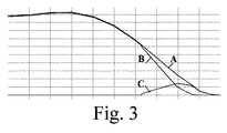
図3においては、図2に示されている第1実施例の波形が示されており、垂直軸は、電力(0ワット乃至8ワット)又は電流(0mA乃至500mA)であり、水平軸は、調光器の導通角(180°乃至0°)である。波形Aは、変換器2を介して伝達される電力(又は変換器3を流れる電流)を示しており、波形Bは、発光ダイオード回路2において放散される電力(又は発光ダイオード回路2を流れる饋電電流)を示しており、波形Cは、ブリーダ回路1において放散される電力(又はブリーダ電流)を示している。この例によれば、ブリーダ回路1なしでは、20%を下回る減光は不可能である。ブリーダ回路1によって、3%までの減光が可能になっている(波形Aと波形Bと間の差)。明らかに、ブリーダ回路1が、所謂深い調光を可能にする。これは、大きな利点である。深い調光における正確な利得は、変換器3の伝達関数に依存する。
In FIG. 3, the waveforms of the first embodiment shown in FIG. 2 are shown, where the vertical axis is power (0 watts to 8 watts) or current (0 mA to 500 mA), and the horizontal axis is It is the conduction angle (180 ° to 0 °) of the dimmer. Waveform A shows the power transmitted through converter 2 (or the current flowing through converter 3), and waveform B shows the power dissipated in light-emitting diode circuit 2 (or the current flowing through light-emitting diode circuit 2). The waveform C indicates the power dissipated in the bleeder circuit 1 (or the bleeder current). According to this example, without the
図4においては、ブリーダ回路1の第2実施例が示されている。ブリーダ回路1の第1入力端子は、ブリーダ回路1の第1出力端子に結合される。ブリーダ回路1の第2入力端子は、ここでは、単一の抵抗器の形態であるが、1つより多くの抵抗器を備える実施例も除外されるべきではない第1抵抗器回路31を介して、ブリーダ回路1の第2出力端子に結合される。ブリーダ回路1は、ここでは、ダーリントン構成の2つのトランジスタの形態であるが、3つ以上のトランジスタを備える実施例も除外されるべきではない第1トランジスタ回路41を有する。第1トランジスタ回路41の第1主電極は、第2抵抗器回路32を介して、ブリーダ回路1の第2出力端子及び第1抵抗器回路31に結合される。第2抵抗器回路32は、単一の抵抗器を有するが、1つより多くの抵抗器を備える実施例も除外されるべきではない。第1トランジスタ回路41の第2主電極は、抵抗器61を介して、ブリーダ回路1の第1出力端子に結合される。抵抗器61は、第1トランジスタ回路41などにおける電力放散を減らす。第1トランジスタ回路41の制御電極は、抵抗器62を介してブリーダ回路1の第1出力端子に結合されると共に、ここでは、単一のトランジスタの形態であるが、2つ以上のトランジスタを備える実施例も除外されるべきではない第2トランジスタ回路42の第2主電極に結合される。第2トランジスタ回路42の第1主電極はアースに結合され、ブリーダ回路1の第2入力端子もアースに結合される。第2トランジスタ回路42の制御電極は、第1トランジスタ回路41の第1主電極に結合される。
In FIG. 4, a second embodiment of the
ブリーダ回路1の出力端子に結合される発光ダイオード回路2を流れる電流の振幅が、小さすぎる値をとるや否や、抵抗器回路31の両端の電圧の振幅は、小さすぎる値をとり、第2トランジスタ回路42は、ブリーダ電流を導入するよう第1トランジスタ回路41を制御する。結果として、発光ダイオード回路2の出力強度が相対的に小さい場合でも、調光器4はトラブルを起こさないだろう。通常、第1抵抗器回路31及び第2抵抗器回路32及び第2トランジスタ回路42が、検出回路11の一部を形成し、第1トランジスタ回路41が、導入回路12の一部を形成する。
As soon as the amplitude of the current flowing through the light emitting
図5においては、ブリーダ回路1の第3実施例が示されている。ブリーダ回路1の第1入力端子は、ブリーダ回路1の第1出力端子に結合される。ブリーダ回路1の第2入力端子は、ここでは単一の抵抗器などの形態の第1抵抗器回路31を介して、ブリーダ回路1の第2出力端子に結合される。ブリーダ回路1は、ここでは単一のトランジスタなどの形態の第1トランジスタ回路41を有する。第1トランジスタ回路41の第1主電極は、第2抵抗器回路32を介して、ブリーダ回路1の第2出力端子及び第1抵抗器回路31に結合される。第2抵抗器回路32は、単一の抵抗器などを有する。第1トランジスタ回路41の第2主電極は、抵抗器61を介して、ブリーダ回路1の第1出力端子などに結合される。第1トランジスタ回路41の制御電極は、抵抗器62を介してブリーダ回路1の第1出力端子に結合されると共に、2つのトランジスタを有するカレントミラー構成53の第1入力部に結合される。カレントミラー構成53の第1出力部は抵抗器74を介してアースに結合され、ブリーダ回路1の第2入力端子もアースに結合される。カレントミラー構成53の第2入力部は、2つのトランジスタを有する差動増幅器構成52の第1出力部に結合される。カレントミラー構成53の第2出力部は、抵抗器73を介してアースに結合される。
In FIG. 5, a third embodiment of the
差動増幅器構成52の第2出力部は、抵抗器72を介してアースに結合される。差動増幅器構成52の給電入力部は、抵抗器71を介して、抵抗器80とコンデンサ81との間の相互接続部に結合される。抵抗器80は、更に、ブリーダ回路1の第1入力端子に結合され、コンデンサ81は、更に、アースに結合される。差動増幅器構成52の第1制御入力部は、抵抗器75を介して前記相互接続部に結合されると共に、抵抗器76を介してアースに結合される。前記相互接続部は、更に、電圧基準素子79を介してアースに結合され、電圧基準素子79の制御電極は、抵抗器77を介して前記相互接続部に結合されると共に、抵抗器78を介してアースに結合される。差動増幅器構成52の第2制御入力部は、第1トランジスタ回路41の第1主電極に結合される。図5に示されているブリーダ回路1の第3実施例は、図4に示されているブリーダ回路1の第2実施例と比べると、差動増幅器構成52及びカレントミラー構成53のために、より良い性能を発揮するだろう。通常、差動増幅器構成52及びカレントミラー構成53は、検出回路11などの一部を形成するだろう。
The second output of
図6においては、ブリーダ回路1の第4実施例が示されている。ブリーダ回路1の第1入力端子は、ブリーダ回路1の第1出力端子に結合される。ブリーダ回路1の第2入力端子は、ここでは単一の抵抗器などの形態の第1抵抗器回路31を介して、ブリーダ回路1の第2出力端子に結合される。ブリーダ回路1は、ここでは単一のトランジスタなどの形態の第1トランジスタ回路41を有する。第1トランジスタ回路41の第1主電極は、第2トランジスタ回路54及び第2抵抗器回路32を介して、ブリーダ回路1の第2出力端子及び第1抵抗器回路31に結合される。第2抵抗器回路32は、単一の抵抗器などを有し、第2トランジスタ回路54の電極を介して第1トランジスタ回路41の第1主電極に結合される。第2トランジスタ回路54は、ここでは、カレントミラー構成の2つのトランジスタを有する。第1トランジスタ回路41の第2主電極は、抵抗器61を介して、ブリーダ回路1の第1出力端子などに結合される。第1トランジスタ回路41の制御電極は、抵抗器62を介してブリーダ回路1の第1出力端子に結合されると共に、カレントミラー構成54の第1入力部に結合される。カレントミラー構成54の第1出力部は、抵抗器91を介して、アースに結合される。カレントミラー構成54の第2入力部及び第2出力部は、前記電極を形成する。通常、カレントミラー構成54は、検出回路11などの一部を形成するだろう。このカレントミラー構成54は、良好な熱安定性を供給する。
FIG. 6 shows a fourth embodiment of the
好ましくは、ブリーダ回路1の第4実施例に示されているように、ブリーダ回路1は、電力消費を減らすためにブリーダ回路1の休止中に検出回路11の少なくとも一部をバイパスするためのバイパス回路13を更に有し得る。バイパス回路13は、例えば、検出回路11の第1抵抗器回路31に対して並列に結合されるダイオード回路92、93を有し得る。このようなダイオード回路92、93は、1つのダイオードを有してもよく、又は例えば直列に結合される2つ以上のダイオードを有してもよい。
Preferably, as shown in the fourth embodiment of the
2つの素子は、第3の素子を介して間接的に結合されてもよく、又は間に第3の素子が結合されずに直接結合されてもよい。示されている前記実施例において、前記実施例のうちの或る実施例の一部は、前記実施例のうちの別の実施例に付加されてもよく、前記実施例のうちの或る実施例の一部は、前記実施例のうちの別の実施例の別の一部に取って代わってもよい。 The two elements may be indirectly coupled via the third element, or may be directly coupled without the third element being coupled therebetween. In the embodiment shown, a part of one of the embodiments may be added to another embodiment of the embodiment, and one embodiment of the embodiment may be added. Some of the examples may replace another part of another of the above embodiments.
要約すると、ブリーダ回路1は、発光ダイオード回路2に給電するための饋電電流の振幅の値を検出するための検出回路11を有すると共に、ブリーダ電流を導入するための導入回路12を有する。ブリーダ電流の振幅の値は、前記検出回路11からの検出結果に応じて規定される。結果として、前記ブリーダ回路1と調光器4との間の不利な接続は回避され、前記ブリーダ回路1は、前記発光ダイオード回路2の近くに位置することができ、それらは、同じヒートシンクを用いることができる。前記検出回路11は、第1抵抗器回路31を有してもよく、前記導入回路12は、第1トランジスタ回路41を有してもよい。前記検出回路11は、前記第1トランジスタ回路41を前記第1抵抗器回路31に結合するための第2抵抗器回路32を更に有してもよく、前記第1トランジスタ回路41を制御するための演算増幅器51又は第2トランジスタ回路42を有してもよい。
In summary, the
本発明を、図面において図示し、上記の説明において詳細に説明しているが、このような図及び説明は、説明的なもの又は例示的なものとみなされるべきであって、限定するものとみなされるべきではない。本発明は、開示されている実施例に限定されない。請求項に記載の発明を実施する当業者は、図面、明細及び添付の請求項の研究から、開示されている実施例に対する他の変形を、理解し、達成し得る。請求項において、「有する」という用語は、他の要素又はステップを除外せず、単数形表記は、複数の存在を除外しない。単に、特定の手段が、相互に異なる従属請求項において引用されているという事実は、これらの手段の組み合わせが有利になるように用いられることができないことを示すものではない。請求項におけるいかなる参照符号も、範囲を限定するものとして解釈されてはならない。 While the invention is illustrated in the drawings and has been described in detail in the foregoing description, such illustration and description are to be considered illustrative and exemplary and limited Should not be considered. The invention is not limited to the disclosed embodiments. Those skilled in the art in practicing the claimed invention may understand and achieve other variations to the disclosed embodiments from a study of the drawings, the specification, and the appended claims. In the claims, the word “comprising” does not exclude other elements or steps, and the singular form does not exclude the presence of a plurality. The mere fact that certain measures are recited in mutually different dependent claims does not indicate that a combination of these measures cannot be used to advantage. Any reference signs in the claims should not be construed as limiting the scope.
Claims (15)
前記発光ダイオード回路の調光動作を改善するためのブリーダ回路であって、
電流の振幅の値を検出するための検出回路、及び
ブリーダ電流を導入するための導入回路であって、前記ブリーダ電流の振幅の値が、前記検出回路からの検出結果に応じて規定される導入回路を含むブリーダ回路と、
饋電電流を供給するための変換器とを有する装置であって、前記検出回路が、前記変換器によって供給される前記饋電電流を検出するよう構成され、前記饋電電流が、前記発光ダイオード回路の少なくとも一部を流れるよう構成され、前記ブリーダ回路と、前記発光ダイオード回路とが、熱的に結合されている装置。 A light emitting diode circuit;
A bleeder circuit for improving the dimming operation of the light emitting diode circuit,
A detection circuit for detecting a current amplitude value ; and
An introduction circuit for introducing a bleeder current, the bleeder circuit including an introduction circuit in which the amplitude value of the bleeder current is defined according to a detection result from the detection circuit;
The apparatus having a converter for supplying the feeder current, the detection circuit is configured to detect the feeder current supplied by the transducer, the feeder current, the light emitting diode An apparatus configured to flow through at least a portion of a circuit, wherein the bleeder circuit and the light emitting diode circuit are thermally coupled .
Applications Claiming Priority (3)
| Application Number | Priority Date | Filing Date | Title |
|---|---|---|---|
| EP13195842.3 | 2013-12-05 | ||
| EP13195842 | 2013-12-05 | ||
| PCT/EP2014/076660 WO2015082661A1 (en) | 2013-12-05 | 2014-12-05 | Bleeder for improving dimming of led |
Publications (3)
| Publication Number | Publication Date |
|---|---|
| JP2016539477A JP2016539477A (en) | 2016-12-15 |
| JP2016539477A5 JP2016539477A5 (en) | 2018-01-18 |
| JP6495911B2 true JP6495911B2 (en) | 2019-04-03 |
Family
ID=49683634
Family Applications (1)
| Application Number | Title | Priority Date | Filing Date |
|---|---|---|---|
| JP2016536244A Active JP6495911B2 (en) | 2013-12-05 | 2014-12-05 | Breeder for improving LED dimming |
Country Status (5)
| Country | Link |
|---|---|
| US (1) | US9949325B2 (en) |
| EP (1) | EP3078243B8 (en) |
| JP (1) | JP6495911B2 (en) |
| CN (1) | CN105794317B (en) |
| WO (1) | WO2015082661A1 (en) |
Families Citing this family (2)
| Publication number | Priority date | Publication date | Assignee | Title |
|---|---|---|---|---|
| CN109392216B (en) * | 2018-03-22 | 2024-03-08 | 陕西亚成微电子股份有限公司 | Method for self-adjusting discharge current and LED silicon controlled rectifier dimming circuit |
| US10652961B2 (en) * | 2018-03-22 | 2020-05-12 | Shaanxi Reactor Microelectronics Co., Ltd | Method for automatically regulating bleeder current and LED silicon-controlled-rectifier dimming circuit |
Family Cites Families (12)
| Publication number | Priority date | Publication date | Assignee | Title |
|---|---|---|---|---|
| JP4943402B2 (en) * | 2008-10-09 | 2012-05-30 | シャープ株式会社 | LED drive circuit, LED illumination lamp, LED illumination device, and LED illumination system |
| KR101888416B1 (en) * | 2009-03-12 | 2018-09-20 | 필립스 라이팅 홀딩 비.브이. | Led lighting with incandescent lamp color temperature behavior |
| JP2011003467A (en) * | 2009-06-19 | 2011-01-06 | Minebea Co Ltd | Lighting system |
| WO2010150158A1 (en) | 2009-06-26 | 2010-12-29 | Koninklijke Philips Electronics N.V. | Lighting arrangement comprising magnetic coding means |
| CN103025337B (en) | 2009-11-17 | 2014-10-15 | 特锐拉克斯有限公司 | LED power-supply detection and control |
| US8476847B2 (en) | 2011-04-22 | 2013-07-02 | Crs Electronics | Thermal foldback system |
| US9210757B2 (en) | 2011-06-10 | 2015-12-08 | Koninklijke Philips N.V. | LED light source |
| EP2596680B1 (en) * | 2011-06-17 | 2017-04-05 | Marvell World Trade Ltd. | Triac dimming systems for solid-state loads |
| US9485830B2 (en) | 2011-07-15 | 2016-11-01 | Citizen Holdings Co., Ltd. | LED lighting apparatus |
| WO2013090700A2 (en) | 2011-12-16 | 2013-06-20 | Terralux, Inc. | Transformer voltage detection in dimmable lighting systems |
| US9508910B2 (en) * | 2011-12-20 | 2016-11-29 | Citizen Holdings Co., Ltd. | LED module |
| US9000683B2 (en) * | 2013-02-26 | 2015-04-07 | Power Integrations, Inc. | Bleeder circuit having current sense with edge detection |
-
2014
- 2014-12-05 CN CN201480066454.7A patent/CN105794317B/en active Active
- 2014-12-05 EP EP14815599.7A patent/EP3078243B8/en active Active
- 2014-12-05 JP JP2016536244A patent/JP6495911B2/en active Active
- 2014-12-05 US US15/038,586 patent/US9949325B2/en active Active
- 2014-12-05 WO PCT/EP2014/076660 patent/WO2015082661A1/en active Application Filing
Also Published As
| Publication number | Publication date |
|---|---|
| US9949325B2 (en) | 2018-04-17 |
| WO2015082661A1 (en) | 2015-06-11 |
| EP3078243B1 (en) | 2019-02-27 |
| EP3078243B8 (en) | 2019-04-10 |
| EP3078243A1 (en) | 2016-10-12 |
| CN105794317B (en) | 2018-11-09 |
| JP2016539477A (en) | 2016-12-15 |
| US20160302272A1 (en) | 2016-10-13 |
| CN105794317A (en) | 2016-07-20 |
Similar Documents
| Publication | Publication Date | Title |
|---|---|---|
| TWI444093B (en) | Control of multi-string led array | |
| Li et al. | Novel self-configurable current-mirror techniques for reducing current imbalance in parallel light-emitting diode (LED) strings | |
| US9888544B2 (en) | Driving circuits and methods for controlling light source | |
| US9900945B1 (en) | Color temperature control | |
| TWI445441B (en) | Driving circuit of light emitting diodes having at least one bypass circuit, and driving method thereof | |
| CN103945601B (en) | LED driver circuit | |
| TW200939870A (en) | Circuit and method for driving light emitting diode | |
| JP2013070598A (en) | Drive power supply and electronic device employing the same | |
| US20140084798A1 (en) | Pfc led driver capable of reducing flicker | |
| JP6495911B2 (en) | Breeder for improving LED dimming | |
| US9629218B1 (en) | Thermal protection for LED bleeder in fault condition | |
| JP6133514B2 (en) | Dynamic control circuit | |
| KR20180120394A (en) | Overvoltage protection device using bypass power consumption means | |
| JP2010118295A (en) | Lighting control device of vehicle lamp | |
| TWI604757B (en) | Line voltage compensation system for LED constant current control | |
| TWI399128B (en) | Method and circuit of controlling an led charge pump driving circuit | |
| JP2014154493A5 (en) | ||
| JP2012240492A (en) | Lighting control circuit of vehicular lighting fixture | |
| TWI493822B (en) | Current dividing circuit | |
| JP6341034B2 (en) | Power supply circuit and lighting device | |
| TWI662859B (en) | Feedback circuit capable of regulating response according to variation of dimming signal | |
| JP2016524274A (en) | AC direct drive LED power supply capable of handling overvoltage | |
| TWI437918B (en) | Light device and power control circuit thereof | |
| KR101397614B1 (en) | Led driving circuit | |
| WO2015183460A4 (en) | Led driver operating from unfiltered mains |
Legal Events
| Date | Code | Title | Description |
|---|---|---|---|
| RD02 | Notification of acceptance of power of attorney |
Free format text: JAPANESE INTERMEDIATE CODE: A7422 Effective date: 20170515 |
|
| RD04 | Notification of resignation of power of attorney |
Free format text: JAPANESE INTERMEDIATE CODE: A7424 Effective date: 20170609 |
|
| A521 | Request for written amendment filed |
Free format text: JAPANESE INTERMEDIATE CODE: A523 Effective date: 20171129 |
|
| A621 | Written request for application examination |
Free format text: JAPANESE INTERMEDIATE CODE: A621 Effective date: 20171129 |
|
| A977 | Report on retrieval |
Free format text: JAPANESE INTERMEDIATE CODE: A971007 Effective date: 20180809 |
|
| A131 | Notification of reasons for refusal |
Free format text: JAPANESE INTERMEDIATE CODE: A131 Effective date: 20180814 |
|
| TRDD | Decision of grant or rejection written | ||
| A01 | Written decision to grant a patent or to grant a registration (utility model) |
Free format text: JAPANESE INTERMEDIATE CODE: A01 Effective date: 20190206 |
|
| A61 | First payment of annual fees (during grant procedure) |
Free format text: JAPANESE INTERMEDIATE CODE: A61 Effective date: 20190307 |
|
| R150 | Certificate of patent or registration of utility model |
Ref document number: 6495911 Country of ref document: JP Free format text: JAPANESE INTERMEDIATE CODE: R150 |
|
| R250 | Receipt of annual fees |
Free format text: JAPANESE INTERMEDIATE CODE: R250 |
|
| R250 | Receipt of annual fees |
Free format text: JAPANESE INTERMEDIATE CODE: R250 |
|
| R250 | Receipt of annual fees |
Free format text: JAPANESE INTERMEDIATE CODE: R250 |