JP6489794B2 - Radiation imaging apparatus, radiation imaging system, and scintillator substrate for radiation imaging apparatus - Google Patents
Radiation imaging apparatus, radiation imaging system, and scintillator substrate for radiation imaging apparatus Download PDFInfo
- Publication number
- JP6489794B2 JP6489794B2 JP2014219662A JP2014219662A JP6489794B2 JP 6489794 B2 JP6489794 B2 JP 6489794B2 JP 2014219662 A JP2014219662 A JP 2014219662A JP 2014219662 A JP2014219662 A JP 2014219662A JP 6489794 B2 JP6489794 B2 JP 6489794B2
- Authority
- JP
- Japan
- Prior art keywords
- scintillator
- partition
- imaging apparatus
- radiation imaging
- radiation
- Prior art date
- Legal status (The legal status is an assumption and is not a legal conclusion. Google has not performed a legal analysis and makes no representation as to the accuracy of the status listed.)
- Active
Links
- 238000003384 imaging method Methods 0.000 title claims description 114
- 230000005855 radiation Effects 0.000 title claims description 80
- 239000000758 substrate Substances 0.000 title claims description 60
- 238000005192 partition Methods 0.000 claims description 246
- 239000011295 pitch Substances 0.000 claims description 40
- 239000000463 material Substances 0.000 claims description 39
- 239000000853 adhesive Substances 0.000 claims description 36
- 230000001070 adhesive effect Effects 0.000 claims description 36
- 239000010410 layer Substances 0.000 description 78
- 238000000034 method Methods 0.000 description 31
- 238000006243 chemical reaction Methods 0.000 description 29
- 239000011229 interlayer Substances 0.000 description 17
- 230000015572 biosynthetic process Effects 0.000 description 13
- 230000008569 process Effects 0.000 description 13
- 230000004048 modification Effects 0.000 description 10
- 238000012986 modification Methods 0.000 description 10
- 239000004820 Pressure-sensitive adhesive Substances 0.000 description 7
- 239000002904 solvent Substances 0.000 description 6
- 238000010521 absorption reaction Methods 0.000 description 5
- 238000001035 drying Methods 0.000 description 5
- 238000012545 processing Methods 0.000 description 5
- 230000004888 barrier function Effects 0.000 description 4
- XQPRBTXUXXVTKB-UHFFFAOYSA-M caesium iodide Chemical compound [I-].[Cs+] XQPRBTXUXXVTKB-UHFFFAOYSA-M 0.000 description 4
- 238000000576 coating method Methods 0.000 description 4
- 239000011521 glass Substances 0.000 description 4
- 229910052751 metal Inorganic materials 0.000 description 4
- 239000002184 metal Substances 0.000 description 4
- 230000003287 optical effect Effects 0.000 description 4
- XUIMIQQOPSSXEZ-UHFFFAOYSA-N Silicon Chemical compound [Si] XUIMIQQOPSSXEZ-UHFFFAOYSA-N 0.000 description 3
- 239000011248 coating agent Substances 0.000 description 3
- 238000001514 detection method Methods 0.000 description 3
- 229910052710 silicon Inorganic materials 0.000 description 3
- 239000010703 silicon Substances 0.000 description 3
- VYPSYNLAJGMNEJ-UHFFFAOYSA-N Silicium dioxide Chemical compound O=[Si]=O VYPSYNLAJGMNEJ-UHFFFAOYSA-N 0.000 description 2
- 229910052782 aluminium Inorganic materials 0.000 description 2
- XAGFODPZIPBFFR-UHFFFAOYSA-N aluminium Chemical compound [Al] XAGFODPZIPBFFR-UHFFFAOYSA-N 0.000 description 2
- 239000011162 core material Substances 0.000 description 2
- 238000011161 development Methods 0.000 description 2
- 238000010586 diagram Methods 0.000 description 2
- 238000010438 heat treatment Methods 0.000 description 2
- 229910010272 inorganic material Inorganic materials 0.000 description 2
- 239000011147 inorganic material Substances 0.000 description 2
- 238000010030 laminating Methods 0.000 description 2
- 238000004519 manufacturing process Methods 0.000 description 2
- 239000011159 matrix material Substances 0.000 description 2
- 239000011368 organic material Substances 0.000 description 2
- 238000000206 photolithography Methods 0.000 description 2
- 239000011241 protective layer Substances 0.000 description 2
- 239000004065 semiconductor Substances 0.000 description 2
- 229910052716 thallium Inorganic materials 0.000 description 2
- BKVIYDNLLOSFOA-UHFFFAOYSA-N thallium Chemical compound [Tl] BKVIYDNLLOSFOA-UHFFFAOYSA-N 0.000 description 2
- OKTJSMMVPCPJKN-UHFFFAOYSA-N Carbon Chemical compound [C] OKTJSMMVPCPJKN-UHFFFAOYSA-N 0.000 description 1
- 239000004593 Epoxy Substances 0.000 description 1
- VGGSQFUCUMXWEO-UHFFFAOYSA-N Ethene Chemical compound C=C VGGSQFUCUMXWEO-UHFFFAOYSA-N 0.000 description 1
- JOYRKODLDBILNP-UHFFFAOYSA-N Ethyl urethane Chemical compound CCOC(N)=O JOYRKODLDBILNP-UHFFFAOYSA-N 0.000 description 1
- 239000005977 Ethylene Substances 0.000 description 1
- 244000043261 Hevea brasiliensis Species 0.000 description 1
- 239000004952 Polyamide Substances 0.000 description 1
- NIXOWILDQLNWCW-UHFFFAOYSA-N acrylic acid group Chemical group C(C=C)(=O)O NIXOWILDQLNWCW-UHFFFAOYSA-N 0.000 description 1
- 229910021417 amorphous silicon Inorganic materials 0.000 description 1
- 230000002238 attenuated effect Effects 0.000 description 1
- 229910052799 carbon Inorganic materials 0.000 description 1
- 239000004918 carbon fiber reinforced polymer Substances 0.000 description 1
- 229920002678 cellulose Polymers 0.000 description 1
- 239000001913 cellulose Substances 0.000 description 1
- 230000008859 change Effects 0.000 description 1
- 238000007796 conventional method Methods 0.000 description 1
- 230000007423 decrease Effects 0.000 description 1
- 230000002950 deficient Effects 0.000 description 1
- 238000003745 diagnosis Methods 0.000 description 1
- 239000003814 drug Substances 0.000 description 1
- 238000005530 etching Methods 0.000 description 1
- PCHJSUWPFVWCPO-UHFFFAOYSA-N gold Chemical compound [Au] PCHJSUWPFVWCPO-UHFFFAOYSA-N 0.000 description 1
- 229910052737 gold Inorganic materials 0.000 description 1
- 239000010931 gold Substances 0.000 description 1
- 230000006872 improvement Effects 0.000 description 1
- 238000007689 inspection Methods 0.000 description 1
- 239000007788 liquid Substances 0.000 description 1
- 238000001459 lithography Methods 0.000 description 1
- 229920003052 natural elastomer Polymers 0.000 description 1
- 229920001194 natural rubber Polymers 0.000 description 1
- 239000004033 plastic Substances 0.000 description 1
- 229920003023 plastic Polymers 0.000 description 1
- 229920002647 polyamide Polymers 0.000 description 1
- 229920000728 polyester Polymers 0.000 description 1
- 239000005020 polyethylene terephthalate Substances 0.000 description 1
- 239000002861 polymer material Substances 0.000 description 1
- 229920000098 polyolefin Polymers 0.000 description 1
- 229920002635 polyurethane Polymers 0.000 description 1
- 239000004814 polyurethane Substances 0.000 description 1
- 239000011347 resin Substances 0.000 description 1
- 229920005989 resin Polymers 0.000 description 1
- 230000000717 retained effect Effects 0.000 description 1
- 238000007789 sealing Methods 0.000 description 1
- 239000000377 silicon dioxide Substances 0.000 description 1
- 239000002356 single layer Substances 0.000 description 1
- 238000000638 solvent extraction Methods 0.000 description 1
- 238000004528 spin coating Methods 0.000 description 1
- 239000000126 substance Substances 0.000 description 1
- 238000007740 vapor deposition Methods 0.000 description 1
Images


Description
本発明は、放射線撮像装置、及び放射線撮像装置用のシンチレータ基板放射線撮像システムに関する。 The present invention relates to a radiation imaging apparatus and a scintillator substrate radiation imaging system for the radiation imaging apparatus.
近年、医療の様々な分野においてデジタル化が進んでおり、X線診断の分野においては、最大で40cm×40cm程度の大面積の放射線撮像装置が開発されている。代表的な放射線撮像装置は、入射する放射線をシンチレータで可視光に変換し、撮像基板に配置された光電変換素子等の変換素子により可視光を電気信号に変換し、画像データを取得するものである。 In recent years, digitization has progressed in various fields of medicine, and in the field of X-ray diagnosis, radiation imaging apparatuses having a large area of up to about 40 cm × 40 cm have been developed. A typical radiation imaging apparatus converts incident radiation into visible light with a scintillator, converts visible light into an electrical signal with a conversion element such as a photoelectric conversion element disposed on an imaging substrate, and acquires image data. is there.
また、医療分野においては、患者の身体情報をより正確に検出するため、鮮鋭度の高い放射線撮像装置が望まれている。例えば、特許文献1のように、シンチレータを隔壁により区分する方法が開示されている。この隔壁に用いられる材料は様々であり、ガラスペースト、金属部材、シンチレータ物質等が考えられる。また、より高精細な隔壁を形成するために、特許文献2に開示されているように、シンチレータを区画する隔壁の材料として低融点ガラス等も用いられることがある。 In the medical field, a radiation imaging apparatus with high sharpness is desired in order to more accurately detect patient physical information. For example, as in Patent Document 1, a method of dividing a scintillator by a partition is disclosed. There are various materials used for the partition walls, and glass paste, metal members, scintillator substances, and the like are conceivable. In order to form a higher-definition partition wall, as disclosed in Patent Document 2, a low-melting-point glass or the like may be used as a partition wall material that partitions the scintillator.
一方、放射線検出装置においては、患者や周囲環境への被ばくや、撮影情報の欠損を防ぐために、放射線検出装置に入射する放射線のできるだけ多くを可視光へ変換することが求められる。そのために、昨今ではシンチレータの厚膜化が進行し、それに伴いシンチレータ層を区画する隔壁も高いものが求められている。 On the other hand, in the radiation detection apparatus, it is required to convert as much of the radiation incident on the radiation detection apparatus as possible into visible light in order to prevent exposure to the patient and the surrounding environment and loss of imaging information. For this reason, in recent years, the scintillator has been made thicker, and accordingly, a high partition wall for partitioning the scintillator layer is also required.
特許文献1では、隔壁層を形成する方法として、ペースト材料の印刷及び乾燥による手法や、成膜、パターン露光及び現像を行うフォトリソグラフィーによる手法等が提案されている。しかし何れの手法においても、一度に形成することができる隔壁の高さは数μm〜数十μmに限られるので、高さの高い隔壁層を形成しようとすると、これらの工程を数回〜数十回繰り返さなければならない。そのため、歩留りが低下するという問題がある。 In Patent Document 1, as a method for forming a partition layer, a method by printing and drying a paste material, a method by photolithography for performing film formation, pattern exposure and development, and the like are proposed. However, in any method, the height of the partition wall that can be formed at one time is limited to several μm to several tens of μm. Therefore, if a partition layer having a high height is to be formed, these steps are performed several times to several times. Must be repeated ten times. Therefore, there is a problem that the yield decreases.
特許文献2では、隔壁ピッチ(P)と隔壁高さ(H)との関係が明記されており、そのアスペクト比(H/P)は0.1〜3.5が好ましいとされている。従って、高さの高い隔壁を形成しようとすると、ピッチが大きくなってしまい、高精細さが失われるという問題がある。 In Patent Document 2, the relationship between the partition pitch (P) and the partition height (H) is specified, and the aspect ratio (H / P) is preferably 0.1 to 3.5. Therefore, if an attempt is made to form a high partition wall, there is a problem that the pitch becomes large and high definition is lost.
以上のように、特許文献1,2等の従来技術では、入射放射線のできるだけ多くを可視光へ変換するためのシンチレータの厚膜化に対応して、高さの高い隔壁層を形成するためには、隔壁層形成時の歩留りや隔壁の高精細さを犠牲にする必要がある。 As described above, in the conventional techniques such as Patent Documents 1 and 2, in order to form a high partition wall layer corresponding to the increase in the thickness of the scintillator for converting as much of the incident radiation as possible into visible light. Therefore, it is necessary to sacrifice the yield when forming the barrier rib layer and the high definition of the barrier rib.
本発明では、上記の問題に対処すべくなされたものであり、形成時の歩留りや高精細さを犠牲にすることなく、高さの高い隔壁部材を形成してシンチレータの実質的な厚膜化を得ることを可能とし、量子検出効率(DQE)に優れた信頼性の高い放射線撮像装置及び放射線撮像システムを提供することを目的とする。 The present invention is made to cope with the above-mentioned problems, and forms a high-thickness partition member without sacrificing the yield and high definition during formation, thereby substantially increasing the thickness of the scintillator. An object of the present invention is to provide a highly reliable radiation imaging apparatus and radiation imaging system excellent in quantum detection efficiency (DQE).
本発明の放射線撮像装置は、放射線を光に変換するシンチレータ基板と、前記シンチレータ基板で変換された光を検出する撮像基板とを備えており、シンチレータ基板は、隔壁によりシンチレータを複数の区画に分割する、高さ方向に積層された複数の隔壁部材を有し、隣り合う前記隔壁部材において、前記隔壁のピッチが異なる。 A radiation imaging apparatus of the present invention includes a scintillator substrate that converts radiation into light, and an imaging substrate that detects light converted by the scintillator substrate, and the scintillator substrate divides the scintillator into a plurality of sections by partition walls. to, have a plurality of partition members that are stacked in the height direction, in the partition wall member adjacent the pitch of the partition walls is different.
本発明のシンチレータ基板は、放射線を光に変換するシンチレータ基板であって、高さ方向に積層された複数の隔壁部材を有し、前記複数の隔壁部材によって備えられた隔壁により放射線を光に変換するシンチレータを複数の区画に分割しており、隣り合う前記隔壁部材において、前記隔壁のピッチが異なる。 The scintillator substrate of the present invention is a scintillator substrate that converts radiation into light, and has a plurality of partition members stacked in the height direction, and converts the radiation into light by the partitions provided by the plurality of partition members. The scintillator to be divided is divided into a plurality of sections, and the pitch of the partition walls is different between the adjacent partition members .
本発明によれば、形成時の歩留りや高精細さを犠牲にすることなく、高さの高い隔壁部材を形成してシンチレータの実質的な厚膜化を得ることを可能とし、DQEに優れた信頼性の高い放射線撮像装置が実現する。 According to the present invention, it is possible to form a high-thickness partition member without sacrificing the yield and high definition at the time of formation, and to obtain a substantially thickened scintillator, which is excellent in DQE. A highly reliable radiation imaging apparatus is realized.
以下、本発明の例示的な諸実施形態について、図面を参照しながら詳細に説明する。 Hereinafter, exemplary embodiments of the present invention will be described in detail with reference to the drawings.
(第1の実施形態)
本実施形態では、放射線撮像装置を開示する。撮像対象の放射線の代表的な例としてX線が挙げられるが、放射線はX線の他、α線、β線、γ線等も含み得る。
(First embodiment)
In the present embodiment, a radiation imaging apparatus is disclosed. A typical example of the radiation to be imaged is X-rays, but the radiation may include α rays, β rays, γ rays, and the like in addition to X rays.
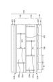
図1は、放射線撮像装置100(以下、単に撮像装置100と言う。)を分解して示す概略斜視図である。撮像装置100は、撮像基板110と、シンチレータ基板120と、撮像基板110とシンチレータ基板120とを接続する接続部材130とを有して構成される。図1において、説明のために撮像基板110、放射線撮像装置用のシンチレータ基板120、及び接続部材130をそれぞれ離間させて描いているが、後述するように実際には撮像基板110とシンチレータ基板120は、接続部材130を介して接続される。
FIG. 1 is an exploded perspective view schematically showing a radiation imaging apparatus 100 (hereinafter simply referred to as an imaging apparatus 100). The
図1において矢印Aで示す方向から被検体に向けて曝射された放射線は、被検体により減衰を受けた後、シンチレータ基板120に入射する。シンチレータ基板120に形成されたシンチレータは、この放射線を光電変換素子が検出可能な波長の光(例えば可視光)に変換する。シンチレータで変換された光は、撮像基板110に入射し、光電変換素子で電気信号に変換され、これによって電気信号が得られる。撮像装置100は、撮像基板110により得られた電気信号に基づいて、例えば信号処理部(不図示)によって画像データを生成する。放射線撮像装置100が放射線の入射から電気信号を得るまでの一連の動作を繰り返し行うことにより、動画像データを得ることもできる。
In FIG. 1, the radiation irradiated toward the subject from the direction indicated by the arrow A is incident on the
図2は、第1の実施形態による撮像装置100の主要構成を示す概略断面図である。撮像装置100において、撮像基板110は、基台111と、基台111上に形成された複数の光電変換素子112と、光電変換素子112を保護する保護層113を有して構成される。
FIG. 2 is a schematic cross-sectional view showing the main configuration of the
基台111は、材料としてはガラス、耐熱性プラスチック等を好適に用いることができる。基板110上に直接的に光電変換素子112を形成する場合以外にも、基台111と光電変換素子112が構築された半導体基板とを、粘着材を介して貼り合わせることで、撮像基板110としても良い。この場合、半導体基板を複数枚タイリングして貼り合わせるようにしても良い。
For the
光電変換素子112は、アモルファスシリコン等の材料からなり、基台111上に所定のピッチでマトリクス状に配置されており、シンチレータ基板120によって放射線から変換された光を電荷に変換する。光電変換素子112の構成は特に限定されず、MIS型センサ、PIN型センサ、TFT型センサ等、適宜用いることができる。信号処理回路及びTFT駆動回路は、撮像基板110外に設けられ、電気的接続部、配線読出し部、配線接続部を介して接続される。
The
シンチレータ基板120は、隔壁によりシンチレータを複数の区画に分割する、高さ方向に積層された複数の隔壁部材を有する。詳細には、シンチレータ基板120は、撮像基板110の直上に設置される第1の隔壁シンチレータ層121と、その上に層間粘着材125を介して積層配置される第2の隔壁シンチレータ層122と、シンチレータ基台123と、粘着材124を有して構成される。第1の隔壁シンチレータ層121は、複数の隔壁121aが所定のピッチP21で並設されて光電変換素子112ごとに対応した区画を形成する第1の隔壁部材121Aを備えており、各区画内にはシンチレータ121bが充填形成されている。第2の隔壁シンチレータ層122は、複数の隔壁122aが所定のピッチP22で並設されて光電変換素子112ごとに対応した区画を形成する第2の隔壁部材122Aを備えており、各区画内にはシンチレータ122bが充填形成されている。第1の隔壁シンチレータ層121と第2の隔壁シンチレータ層122とは、隔壁121aと隔壁122aとが先端で付き合わされるように、層間粘着材125で接着されている。第2のシンチレータ層122は、粘着材124によってシンチレータ基台123に固定されている。第1及び第2の隔壁シンチレータ層121,122は、シンチレータ基板120の上方で面状に一様に広がっており、一体になっていても良く、また小さいサイズのものが複数個タイリングしてあっても良い。
The
隔壁121a,122aのピッチP21,P22は、適宜選択することが可能であるが、光電変換素子112のピッチP1(1個の光電変換素子112に対応したピッチ)の整数倍であることが望ましい。本実施形態では、P1,P21,P22は同一とされている。ピッチP21,P22をこのように設定することにより、夫々の光電変換素子112上に配置される第1及び第2のシンチレータ122a,122bの量のばらつきを抑え、撮影画像の歪み等を軽減することができる。
The pitches P21 and P22 of the
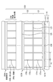
図3は、第1の実施形態による撮像装置100について、光電変換素子及び第2の隔壁部材のみを示す概略平面図である。撮像基板110には、破線で示す複数の光電変換素子112がマトリクス状に配置されている。図3においては説明のため、光電変換素子112の輪郭を破線で示しているが、実際の撮像基板110上にはこのような破線は存在しない。各光電変換素子112は隣り合う光電変換素子112と所定のピッチP1で配置されている。ピッチP1を維持することにより、得られる画像の歪み等を軽減することができる。第2の隔壁部材122Aは、その下方に存する不図示の第1の隔壁シンチレータ層121と共に、隔壁122a(及び隔壁121a)により光電変換素子112ごとに区画している。
FIG. 3 is a schematic plan view showing only the photoelectric conversion element and the second partition member in the
接続部材130としては、両面粘着の粘着シート、液体硬化タイプの粘着材、又は接着剤等が用いられる。特に好適には、光学用粘着シート又は粘着材が用いられる。これは、放射線がシンチレータに入射して発生した蛍光発光を、撮像基板110にロスなく到達させるためである。故に、接続部材130はシンチレータ層の発光波長に対して吸収を持たないことが望ましい。接続部材130の厚みは5μm〜100μm程度が望ましく、5μm〜25μmが更に望ましい。接続部材130の厚みが5μm未満であるとすると、十分な粘着力が得られず、シンチレータ基板120と撮像基板110とが剥離する可能性が生じる。接続部材130の厚みが100μm以上であるとすると、シンチレータ基板120で発生した光の、接続部材130での散乱が大きくなってしまい、放射線撮像装置として取得される画像の解像度が低下してしまう虞がある。接続部材130の材料としては、有機材料、無機材料の何れを用いても良い。例えば、アクリル系、エポキシ系、シリコン系、天然ゴム系、シリカ系、ウレタン系、エチレン系、ポリオレフィン系、ポリエステル系、ポリウレタン系、ポリアミド系、セルロース系等が適宜用いられる。これらは単体でも混合でも用いられる。また、粘着シートの構造としては、PET等の芯材の両面に粘着層を形成したもの、芯材なしで単層の粘着層としてシート化されたもの等が用いられる。
As the
シンチレータ基台123の材料としては、有機材料及び無機材料の何れを用いても良い。カーボン、CFRP、高分子材料、PET、アルミ等が用いられ、放射線吸収の小さい材料が好ましい。シンチレータ基台123は、反射板として用いても良い。その場合、アルミや金等の反射率の高い金属、高反射率のPET等の材料が用いられる。又は、PET等の表面に反射加工を施されて用いられる。
As a material of the
粘着材124は、基本的には接続部材130と相違しない。但し、第1又は第2の隔壁部材121A,122Aが撮像基板110又はシンチレータ基台124に直接的に形成される場合には、粘着材124は使用しなくても良い。
The
層間粘着材125は、基本的には接続部材130と相違しない。実施態様によっては使用しない場合もあり得る。層間粘着材125の厚みは1μm〜100μm程度であることが望ましい。好適には、1μm〜25μm程度が更に望ましい。層間粘着材125の厚みが5μm未満であるとすると、十分な粘着力が得られないので、後にシンチレータ基板120全体の周囲を封止する等の別途の固定手段が必要になる。層間粘着材125の厚みが100μm以上であるとすると、シンチレータ基板120で発生した光の、接続部材130における散乱が大きくなってしまい、放射線撮像装置として取得される画像の解像度が低下する虞がある。
The
本実施形態では、シンチレータ基板120は、隔壁部材が2層の積層構造とされており、隔壁121a,122aによりシンチレータ121b,122bを複数の区画に分割する、高さ方向に積層された第1及び第2の隔壁部材121A,122Aを有する。この構成により、高さの高い単層の隔壁部材を形成する場合に比べて、歩留りが向上し、隔壁高さを低く抑えることでアスペクト比を所期の適正範囲内の値に調節して高精細を確保することができる。
In the present embodiment, the
以下、本実施形態による上記の歩留り向上について詳述する。先述の通り、特許文献1では、隔壁層を形成する手段として、ペースト材料の印刷及び乾燥による手法や、成膜、パターン露光及び現像を行うフォトリソグラフィーによる手法等が提案されている。しかしながら何れの手法においても、一度に形成できる隔壁部材の高さは数μm〜数十μmに限られるので、高さの高い隔壁層を形成しようとすると、これらの工程を数回〜数十回繰り返さなければならない。 Hereinafter, the yield improvement according to the present embodiment will be described in detail. As described above, Patent Document 1 proposes a technique of printing and drying a paste material, a technique of photolithography that performs film formation, pattern exposure, and development as means for forming a partition layer. However, in any method, the height of the partition member that can be formed at one time is limited to several μm to several tens of μm. Therefore, when a high-partition barrier layer is formed, these steps are performed several times to several tens of times. Must be repeated.
特許文献1に記載された隔壁層の形成方法において、一回のプロセスで形成できる隔壁の高さをt、そのプロセスの歩留まり率をyとすると、例えば高さ10tの隔壁を形成する場合には、プロセスを10回繰り返すため、歩留まり率はy10となる。これに対して、本実施形態では、隔壁部材を2層に積層するため、例えば10tの高さの隔壁を形成する場合でも、5tの隔壁部材を2つ形成すれば良い。そのため、同じ手法で2つの隔壁部材を形成しても、歩留まり率はy5となる。なお、隔壁部材の貼り合わせ工程については無視している。即ち、本実施形態では、特許文献1に比べてプロセスを繰り返す回数が半分になる。 In the method of forming a partition layer described in Patent Document 1, when the height of the partition wall that can be formed in one process is t and the yield rate of the process is y, for example, when a partition wall having a height of 10 t is formed. Since the process is repeated 10 times, the yield rate is y 10 . On the other hand, in this embodiment, since the partition wall members are stacked in two layers, for example, even when a 10t-high partition wall is formed, two 5t partition members may be formed. Therefore, even if two partition members are formed by the same method, the yield rate is y 5 . In addition, the bonding process of the partition member is ignored. That is, in the present embodiment, the number of times the process is repeated is halved compared to Patent Document 1.
隔壁部材の形成プロセスにおける一回当たりの歩留まり率をy、得られる高さをt、形成したい高さをn×tとすると、歩留まり率はynとなる。これに対して本実施形態では、歩留まり率はyn/2となる。例えばy=90%、t=10μm、形成したい高さ=100μmとすると、特許文献1では、歩留まり率=(0.910)×100≒34%となる。これに対して本実施形態では、歩留まり率=(0.95)×100≒59%となり、特許文献1の場合と歩留まり率で25%程度の差異が生じる。 Y the yield rate per one in the formation process of the partition wall member, the height obtained t, the height to be formed when the n × t, yield rate is y n. On the other hand, in this embodiment, the yield rate is yn / 2 . For example, if y = 90%, t = 10 μm, and the height to be formed = 100 μm, in Patent Document 1, the yield ratio = (0.9 10 ) × 100≈34%. On the other hand, in the present embodiment, the yield rate = (0.9 5 ) × 100≈59%, and a difference of about 25% occurs in the yield rate from the case of Patent Document 1.
以下、撮像装置100の主要構成の形成方法について説明する。先ず、第1及び第2の隔壁部材121A,122Aの作製について述べる。隔壁部材の材料としてはシリコン、金属、ガラス等が好適に用いられる。高反射且つ遮光性の高い材料であり、高いアスペクト比におけるエッチングが可能な材料であれば、適宜用いることができる。また、表面に金属膜を形成したものや、反射部材を一様に含有したもの、シンチレータを含有した樹脂等も用いられることがある。例えば、初期のパターンのマスクを利用してマスクに対して上記の材料を成膜し、マスクを除去した後に乾燥することにより、第1及び第2の隔壁部材121A,122Aが形成される。また、上記の材料上にマスクを形成し、材料をリソグラフィー及びエッチングした後、マスクを除去して乾燥することにより、第1及び第2の隔壁部材121A,122Aを形成しても良い。これらの手法では、基台上に直接的に隔壁部材が形成されるか、又は基台そのものが隔壁部材となる。また、複数個の隔壁部材をタイリングする手法では、特にシリコンウェハをエッチングして所定のピッチで区画を形成し、ダイシングにより小さいサイズに切り出した後、タイリングする方法等がある。この手法では、基台上に、粘着材を介して隔壁部材が設置される。
Hereinafter, a method for forming the main configuration of the
続いて、撮像基板110上に第1の隔壁部材121Aを接続部材130を介して貼り合わせた後、隔壁121aで区切られた区画内にシンチレータ121bを形成する。詳細には例えば、形成された第1の隔壁部材121Aの上からシンチレータ材料と溶剤、又は接着部材と混合したシンチレータ溶液を塗布し、隔壁121aで区切られた各区画内にシンチレータ溶剤を充填する。シンチレータ材料としては、GOS又はTl(タリウム)をドープした柱状のCsI(ヨウ化セシウム)等が挙げられる。その後、全体を加熱処理することで、溶剤の除去及び接着部材の硬化を行う。以上により、第1の隔壁部材121Aの各区画内をシンチレータ121bで充填された第1の隔壁シンチレータ層121が形成される。
Subsequently, after the
シンチレータ溶剤の塗布方法としては、スピン塗布、スリット塗布、印刷塗布等がある。また、溶剤の作製の段階で脱法工程を導入したり、塗布時に真空環境下で行うこと等により、シンチレータ121b内の気泡の発生を防止することができる。或いは、先に塗布及び蒸着等によりシンチレータのみの層を形成し、当該シンチレータ層に第1の隔壁部材121Aを突き刺すことで、第1の隔壁シンチレータ層121を形成することができる。この場合、シンチレータ層に第1の隔壁部材121Aを突き刺すタイミングとしては、加熱等でシンチレータ層が硬化・成形される前であっても、シンチレータ層が完全に成形された後であっても良い。シンチレータ121bの厚みは1700μm以下の値とする。実際に医療現場において使用する管電圧下においては、シンチレータの厚みが凡そ1700μmでX線吸収率が100%に達してしまい、これ以上膜厚を厚くしてもX線吸収率に変化がないためである。
Examples of the scintillator solvent coating method include spin coating, slit coating, and printing coating. In addition, by introducing a deprocessing process at the stage of producing the solvent or by performing it in a vacuum environment at the time of application, it is possible to prevent the generation of bubbles in the
一方、シンチレータ基台123上に第2の隔壁部材122Aを粘着材124を介して貼り合わせた後、隔壁122aで区切られた区画内に第2のシンチレータ122bを形成する。このときの詳細については、第1の隔壁シンチレータ層121の形成時と同様である。以上により、第2の隔壁部材122Aの各区画内をシンチレータ122bで充填された第2の隔壁シンチレータ層122が形成される。
On the other hand, after the
第1の隔壁部材121A(第2の隔壁部材122A)の厚み(高さ)とシンチレータ121b(シンチレータ122b)の厚み(高さ)とは、必ずしも一致しなくても良いが、シンチレータ121b(シンチレータ122b)の厚みの方が大きいことが望ましい。第1の隔壁部材121A(第2の隔壁部材122A)がシンチレータ121b(シンチレータ122b)から突き出ると、設置した際にシンチレータ121b(シンチレータ122b)内に空気層が形成される。これにより、光学特性が著しく失われ、撮影画像に歪みが生じるためである。
The thickness (height) of the
第1又は第2の隔壁部材121A,122Aの一方若しくは双方を、シンチレータ121b,122bの厚みよりも厚く形成し、第1又は第2の隔壁部材121A,122Aを突き出させるようにしておいて、層間粘着材125に突き刺す方法も考えられる。この場合、第1又は第2の隔壁部材121A,122Aの突き出させる高さ等は層間粘着材125の部材によるが、何れにせよ、空気を抱き込まないようにする必要がある。また、第1の隔壁部材121Aの高さと第2の隔壁部材122Aの高さとは、必ずしも同じでなくても構わない。
One or both of the first or
以上のようにして作製された、撮像基台110に貼り合わされた第1の隔壁シンチレータ層121と、シンチレータ基台123に貼り合わされた第2の隔壁シンチレータ層122とを、層間粘着材125で貼り合わせる。以上により、撮像装置100の主要構成が形成される。当該主要構成を構成する各部材、又はその何れかにアライメント用のマーキングを設けることにより、第1の隔壁シンチレータ層121及び第2の隔壁シンチレータ層122を狙った位置にずれなく設置して貼り合わせることができる。また、このように第1の隔壁シンチレータ層121と第2の隔壁シンチレータ層122を別個に作製し、それぞれを検査することで、良品同士のみを貼り合わせることができる。図2中では、P1=P21=P22として描いているが、これらのピッチは必ずしも一致しなくても良い。好適には、それぞれのピッチの関係は何れかのピッチの整数倍同士であることが望ましい。これは、それぞれの光電変換素子112上に配置されるシンチレータ122bの量のばらつきを抑えることにより、撮影画像の歪み等を軽減するためである。
The first partition
層間粘着材125の貼り合わせは、第1の隔壁シンチレータ層121側、第2の隔壁シンチレータ層122側の何れから行っても良い。この際、第1又は第2の隔壁シンチレータ層121,122と層間粘着材125との間に気泡が混入すると、気泡存在箇所における光学特性が著しく変化し、撮影画像ではノイズとなる。従って層間粘着材125の貼り合わせは、ラミネート工程、真空工程、脱法工程、加熱工程、加圧工程等で気泡の抱き込みのないように行う必要がある。
The bonding of the
以上説明したように、本実施形態によれば、形成時の歩留りや高精細さを犠牲にすることなく、第1及び第2の高さの高い隔壁部材121A,122Bを形成してシンチレータの実質的な厚膜化を得ることを可能とし、DQEに優れた信頼性の高い撮像装置100が実現する。
As described above, according to the present embodiment, the first and second high
(第2の実施形態)
本実施形態では、第1の実施形態と同様に放射線撮像装置を開示するが、上下の隔壁シンチレータ層間の接続部材が異なる点で第1の実施形態と相違する。
(Second Embodiment)
This embodiment discloses a radiation imaging apparatus as in the first embodiment, but differs from the first embodiment in that connection members between upper and lower partition wall scintillator layers are different.
図4は、第2の実施形態による撮像装置100の主要構成を示す概略断面図である。撮像装置100において、第1の隔壁シンチレータ層121と第2の隔壁シンチレータ層122とが層間シンチレータ126で接続される。層間シンチレータ126の材料としては、GOS又はTl(タリウム)をドープした柱状のCsI(ヨウ化セシウム)等が挙げられる。また、これらと溶剤又は接着剤を混合させたシンチレータ溶液を用いても良い。シンチレータ基板120のシンチレータ121b,122bと同じ材料でも良いし、異なる材料を用いても良い。
FIG. 4 is a schematic cross-sectional view showing the main configuration of the
本実施形態によれば、形成時の歩留りや高精細さを犠牲にすることなく、高さの高い第1及び第2の隔壁部材121A,122Aを形成してシンチレータの実質的な厚膜化を得ることを可能とし、DQEに優れた信頼性の高い撮像装置100が実現する。更に本実施形態では、第1及び第2の隔壁シンチレータ層121,122間に層間シンチレータ126が配置されることにより、撮像装置100に入射する放射線の可視光への変換効率(変換量)が層間シンチレータ126の厚み分だけ増加する。
According to the present embodiment, the first and second
(第3の実施形態)
本実施形態では、第1の実施形態と同様に放射線撮像装置を開示するが、上下の隔壁シンチレータ層間においてシンチレータを共有する点で第1の実施形態と相違する。
(Third embodiment)
In the present embodiment, the radiation imaging apparatus is disclosed as in the first embodiment, but is different from the first embodiment in that the scintillator is shared between the upper and lower partition wall scintillator layers.
図5は、第3の実施形態による撮像装置100の主要構成を示す概略断面図である。撮像装置100において、第1の隔壁シンチレータ層121と第2の隔壁シンチレータ層122との間には粘着材等の接合部材は設置されておらず、シンチレータを共有することで接続されている。第1及び第2の隔壁シンチレータ層121,122間の貼り合わせに粘着材を用いず、シンチレータ121b,122bが一体化している。この構成により、シンチレータ基板120内における蛍光の散乱を防止し、蛍光に直進性を持たせることができる。また、工数減及び粘着部材分のコストダウンも望める。
FIG. 5 is a schematic cross-sectional view showing the main configuration of the
以下、撮像装置100の主要構成の形成方法について説明する。先ず、第1及び第2の隔壁シンチレータ層121,122の作製方法については第1の実施形態の場合と同様である。続いて、図6に示すように、撮像基板110上に第1の隔壁部材121Aを接続部材130を介して貼り合わせた後、隔壁121aで区切られた区画内及び隔壁121aを覆うように、シンチレータ127を隔壁121aよりも厚く(高く)形成する。一方、シンチレータ基台123上に第2の隔壁部材122Aを粘着材124を介して貼り合わせる。そして、第2の隔壁部材122Aを第1の隔壁部材121Aを覆うシンチレータ127に突き刺し、隔壁同士、即ち隔壁121a,122aの先端同士を接触させる。この際、第1及び第2の隔壁部材121A,122Aにおいてシンチレータ127を共有する。第1の隔壁部材121Aの各区画を充填する部分のシンチレータをシンチレータ121bとし、第2の隔壁部材122Aの各区画を充填する部分のシンチレータをシンチレータ122bとして、第1及び第2の隔壁シンチレータ層121,122が形成される。
Hereinafter, a method for forming the main configuration of the
第2の隔壁部材122Aを第1の隔壁部材121Aを覆うシンチレータに突き刺すに際して、シンチレータ127の厚みを、第1の隔壁部材121Aの高さと第2の隔壁部材121Bの高さとを加算した値以上とする。シンチレータ127の厚みが当該加算値に満たないと、隔壁121a,122aの先端同士を接触させるときに隔壁121a,122aが損壊する虞がある。或いは、第2の隔壁部材122Aの区画内に十分にシンチレータ127が充填されず、空気層が形成されてしまう。
When the
第2の隔壁部材122Aを第1の隔壁部材121Aを覆うシンチレータに突き刺すタイミングとしては、シンチレータが完全に形成されてからでも、シンチレータ127を形成する工程の途中でも良い。工程の途中で突き刺す場合としては、例えば、シンチレータ127を塗布した後、乾燥する前に第2の隔壁部材122Aを突き刺し、一体となったシンチレータ基板120ごと乾燥させる。
The timing of piercing the
また、隔壁121aで区切られた区画内及び隔壁121aを覆うようにシンチレータを隔壁121aよりも厚く(高く)形成し、第1の隔壁部材121Aを覆う当該シンチレータに第2の隔壁部材122Aを突き刺すようにしても良い。
Further, a scintillator is formed thicker (higher) than the
本実施形態によれば、形成時の歩留りや高精細さを犠牲にすることなく、高さの高い第1及び第2の隔壁部材121A,122Aを形成してシンチレータの実質的な厚膜化を得ることを可能とし、DQEに優れた信頼性の高い撮像装置100が実現する。
According to the present embodiment, the first and second
−変形例−
以下、第3の実施形態の変形例について説明する。この変形例では、第3の実施形態の同様に放射線撮像装置を開示するが、そのシンチレータ基板の構造が異なる点で第3の実施形態と相違する。
-Modification-
Hereinafter, modifications of the third embodiment will be described. In this modification, a radiation imaging apparatus is disclosed as in the third embodiment, but differs from the third embodiment in that the structure of the scintillator substrate is different.
図7は、第3の実施形態の変形例による撮像装置100の主要構成を示す概略断面図である。撮像装置100において、第3の実施形態と同様に、第1の隔壁シンチレータ層121と第2の隔壁シンチレータ層122との間には粘着材等の接合部材は設置されておらず、シンチレータを共有することで接続されている。この構成により、シンチレータ基板120内における蛍光の散乱を防止し、蛍光に直進性を持たせることができる。また、工数減及び粘着部材分のコストダウンも望める。
FIG. 7 is a schematic cross-sectional view showing the main configuration of the
本例によれば、形成時の歩留りや高精細さを犠牲にすることなく、高さの高い第1及び第2の隔壁部材121A,122Aを形成してシンチレータの実質的な厚膜化を得ることを可能とし、DQEに優れた信頼性の高い撮像装置100が実現する。また、第1及び第2の隔壁部材121A,122Aがシンチレータ121b,122bを共有し、隔壁121a,122aの先端同士が離間して対向配置され、隔壁121a,122aの先端同士が非接触の状態で保持される。この構成により、第2の隔壁部材122A(第1の隔壁部材121A)を第1の隔壁部材121A(第2の隔壁部材122A)を覆うシンチレータに突き刺す際における当該先端同士の接触による隔壁121a,122aの損壊が確実に防止される。
According to this example, the first and second
(第4の実施形態)
本実施形態では、第1の実施形態と同様に放射線撮像装置を開示するが、上下の隔壁シンチレータ層間の隔壁のピッチがずれている点で第1の実施形態と相違する。
(Fourth embodiment)
In the present embodiment, the radiation imaging apparatus is disclosed as in the first embodiment, but differs from the first embodiment in that the pitch of the partition walls between the upper and lower partition scintillator layers is shifted.
図8は、第4の実施形態による撮像装置100の主要構成を示す概略断面図である。撮像装置100では、第1及び第2の隔壁シンチレータ層121,122において、第1の隔壁部材121Aの隔壁121aと第2の隔壁シンチレータ層122の隔壁122aとが平面方向に対向位置からずれて、ピッチをずらして配置されている。ここでは、隔壁121a,122aが半ピッチずらして配置されている。このように隔壁121a,122aについてピッチをずらして配置することにより、第1及び第2の隔壁部材121A,122Aで形成可能な最小ピッチの隔壁よりも、更に小さなピッチで隔壁121a,122aを設置することができる。例えば図7中では、P21=P22=2×P1とし、隔壁121a,122aについて半ピッチずらして設置されている。この構成により、第1及び第2の隔壁部材121A,122Aの各々についてはピッチを2×P1とするも、第1及び第2の隔壁部材121A,122Aを一体化させた際には半分のP1のピッチで隔壁121a,122aを配置することができる。
FIG. 8 is a schematic cross-sectional view showing the main configuration of the
本実施形態によれば、形成時の歩留りや高精細さを犠牲にすることなく、高さの高い第1及び第2の隔壁部材121A,122Aを形成してシンチレータの実質的な厚膜化を得ることを可能とし、DQEに優れた信頼性の高い撮像装置100が実現する。
According to the present embodiment, the first and second
−変形例−
以下、第4の実施形態の変形例について説明する。この変形例では、第4の実施形態の同様に放射線撮像装置を開示するが、そのシンチレータ基板の構造が異なる点で第4の実施形態と相違する。
-Modification-
Hereinafter, a modification of the fourth embodiment will be described. In this modification, a radiation imaging apparatus is disclosed as in the fourth embodiment, but differs from the fourth embodiment in that the structure of the scintillator substrate is different.
図9は、第4の実施形態の変形例による撮像装置100の主要構成を示す概略断面図である。撮像装置100において、第3の実施形態と同様に、第1の隔壁シンチレータ層121と第2の隔壁シンチレータ層122との間には粘着材等の接合部材は設置されておらず、シンチレータを共有することで接続している。この構成により、シンチレータ基板120内における蛍光の散乱を防止し、蛍光に直進性を持たせることができる。また、工数減及び粘着部材分のコストダウンも望める。
FIG. 9 is a schematic cross-sectional view showing the main configuration of an
第1及び第2の隔壁シンチレータ層121,122において、第1の隔壁部材121Aの隔壁121aと第2の隔壁シンチレータ層122の隔壁122aとが平面方向にピッチをずらして配置されている。ここでは、第1及び第2の隔壁シンチレータ層121,122でシンチレータを共有し、隔壁121a,122aが半ピッチずらして配置されている。このように隔壁121a,122aについてピッチをずらして配置することにより、第1及び第2の隔壁部材121A,122Aで形成可能な最小ピッチの隔壁よりも、更に小さなピッチで隔壁121a,122aを設置することができる。また、隔壁121aは第2の隔壁部材122Aの底面と、隔壁122aは第1の隔壁部材121Aの底面とそれぞれ離間しており、非接触の状態で保持される。この構成により、第2の隔壁部材122A(第1の隔壁部材121A)を第1の隔壁部材121A(第2の隔壁部材122A)を覆うシンチレータに突き刺す際における当該先端同士の接触による隔壁121a,122aの損壊が確実に防止される。
In the first and second partition wall scintillator layers 121 and 122, the
本例によれば、形成時の歩留りや高精細さを犠牲にすることなく、高さの高い第1及び第2の隔壁部材121A,122Aを形成してシンチレータの実質的な厚膜化を得ることを可能とし、DQEに優れた信頼性の高い撮像装置100が実現する。
According to this example, the first and second
(第5の実施形態)
本実施形態では、第1の実施形態と同様に放射線撮像装置を開示するが、上下の隔壁シンチレータ層間の隔壁のピッチが異なる点で第1の実施形態と相違する。
(Fifth embodiment)
In the present embodiment, a radiation imaging apparatus is disclosed as in the first embodiment, but differs from the first embodiment in that the pitch of the partition walls between the upper and lower partition scintillator layers is different.
図10は、第5の実施形態による撮像装置100の主要構成を示す概略断面図である。撮像装置100では、第1及び第2の隔壁シンチレータ層121,122において、第1の隔壁部材121Aの隔壁121aのピッチP21と第2の隔壁シンチレータ層122の隔壁122aのピッチP22とが異なる。好適には一方のピッチが他方のピッチの整数倍になるようにする。図9中では、P21=2×P22とされている。
FIG. 10 is a schematic cross-sectional view showing the main configuration of the
このように、第1及び第2の隔壁シンチレータ層121,122で隔壁121a,122aのピッチを異ならしめることで、シンチレータ基板120内におけるシンチレータ特性を容易に制御することができる。具体的には、以下の構造(1)〜(3)を選択的に形成することが可能となる。構造(1)は、撮影画像の鮮鋭度をより重視した構造であり、光電変換素子112上のシンチレータが可及的に隔壁で区切られる。構造(2)は、シンチレータにおける放射線の変換効率や輝度をより重視した構造であり、可及的に多くの蛍光が光電変換素子112に入射する構造であって、隔壁数は少ない。構造(3)は、構造(1),(2)の双方のバランスを適宜調整した構造である。
Thus, by making the pitches of the
本実施形態によれば、形成時の歩留りや高精細さを犠牲にすることなく、第1及び第2の高さの高い隔壁部材121A,122Bを形成してシンチレータの実質的な厚膜化を得ることを可能とし、DQEに優れた信頼性の高い撮像装置100が実現する。
According to the present embodiment, the first and second high
(第6の実施形態)
以下、第6の実施形態について説明する。本実施形態では、第1の実施形態の同様に放射線撮像装置を開示するが、そのシンチレータ基板の構造が異なる点で第1の実施形態と相違する。
(Sixth embodiment)
The sixth embodiment will be described below. In the present embodiment, a radiation imaging apparatus is disclosed as in the first embodiment, but is different from the first embodiment in that the structure of the scintillator substrate is different.
図11は、第6の実施形態による撮像装置100の主要構成を示す概略断面図である。撮像装置100では、第1の実施形態の構成に加え、第2の隔壁シンチレータ層122上に更に隔壁シンチレータ層を積層されている。nを3以上の整数として、n層の隔壁シンチレータ層が積層されることになる。図10では、n層目の隔壁シンチレータ層200は、隔壁部材200A及びその隔壁200aで区切られた区画内を充填するシンチレータ200bを有して構成される。
FIG. 11 is a schematic cross-sectional view showing the main configuration of the
隔壁シンチレータ層を3層以上に積層することにより、隔壁部材のピッチを小さく保ったまま、シンチレータ基板をより厚く形成することができる。但し、n層重ね合わせたシンチレータの総厚を1700μm以下にする必要がある。実際に医療現場において使用する管電圧下においては、シンチレータの厚みが凡そ1700μmでX線吸収率が100%に達してしまい、シンチレータの総厚をこれ以上厚くしてもX線吸収率に変化がないためである。 By laminating the partition wall scintillator layers into three or more layers, the scintillator substrate can be formed thicker while keeping the pitch of the partition wall members small. However, it is necessary that the total thickness of the scintillators with n layers stacked be 1700 μm or less. Under the tube voltage actually used in the medical field, the scintillator thickness is about 1700 μm and the X-ray absorption rate reaches 100%. Even if the total thickness of the scintillator is increased further, the X-ray absorption rate changes. This is because there is not.
本実施形態によれば、形成時の歩留りや高精細さを犠牲にすることなく、第1及び第2の高さの高い隔壁部材121A,122Bを形成してシンチレータの実質的な厚膜化を得ることを可能とし、DQEに優れた信頼性の高い撮像装置100が実現する。
According to the present embodiment, the first and second high
(第7の実施形態)
本実施形態では、第1〜第6の実施形態又は諸変形例の撮像装置100を適用した、放射線検査装置等に代表される放射線撮像システムについて例示する。図12は、第7の実施形態による放射線撮像システムの概略構成を示す模式図である。
(Seventh embodiment)
In the present embodiment, a radiation imaging system represented by a radiation inspection apparatus or the like to which the
放射線撮像システムは、X線ルーム300内に配置される。放射線撮像システムは、放射線を発生させるための放射線源であるX線チューブ301と、撮像装置100と、イメージプロセッサ302を含む信号処理部と、ディスプレイ303を含む表示部とを備えて構成される。撮像装置100は、第1〜第6の実施形態及び諸変形例から選ばれた1種の放射線撮像装置である。
The radiation imaging system is disposed in the X-ray room 300. The radiation imaging system includes an X-ray tube 301 that is a radiation source for generating radiation, the
X線チューブ301で発生したX線311は、患者等の被検者312の胸部313を透過し、撮像装置100に入射する。この入射したX線には被検者320の体内部の情報が含まれている。撮像装置100では、入射したX線311に応じた電気的情報が得られる。その後、この電気的情報はデジタル変換され、イメージプロセッサ330により画像処理され、ディスプレイ303により表示される。
X-rays 311 generated by the X-ray tube 301 pass through the chest 313 of the subject 312 such as a patient and enter the
上記の電気的情報は、電話、LAN、インターネット等のネットワーク320により遠隔地へ転送される。これにより、ドクタールーム300等の別の場所におけるディスプレイ401に表示して、遠隔地の医師が診断することが可能である。また、上記の電気的情報は、例えば、光ディスク等に保存することもできるし、フィルムプロセッサ402によってフィルム403等の記録部に記録することもできる。 The electrical information is transferred to a remote place via a network 320 such as a telephone, a LAN, or the Internet. Thereby, it can display on the display 401 in another places, such as the doctor room 300, and a doctor of a remote place can diagnose. In addition, the electrical information can be stored, for example, on an optical disk or the like, or can be recorded on a recording unit such as the film 403 by the film processor 402.
100 放射線撮像装置
110 撮像基板
111 基台
112 光電変換素子
113 保護層
120 シンチレータ基板
121 第1の隔壁シンチレータ層
121A 第1の隔壁部材
121a,122a,200a 隔壁
121b,122b,200b シンチレータ
122 第2の隔壁シンチレータ層
122A 第2の隔壁部材
123 シンチレータ基台
124 粘着材
125 層間粘着材
126 層間シンチレータ
130 接続部材
200 隔壁シンチレータ層
200A 隔壁部材
DESCRIPTION OF
Claims (9)
前記シンチレータ基板で変換された光を検出する撮像基板と
を備えており、
シンチレータ基板は、隔壁によりシンチレータを複数の区画に分割する、高さ方向に積層された複数の隔壁部材を有し、
隣り合う前記隔壁部材において、前記隔壁のピッチが異なることを特徴とする放射線撮像装置。 A scintillator substrate that converts radiation into light;
An imaging substrate for detecting light converted by the scintillator substrate,
The scintillator substrate divides the scintillator into a plurality of compartments by partition walls, have a plurality of partition members that are stacked in the height direction,
The radiation imaging apparatus , wherein the partition walls adjacent to each other have different pitches between the partition walls .
請求項1〜7のいずれか1項に記載の放射線撮像装置と
を備えることを特徴とする放射線撮像システム。 A radiation source that generates radiation; and
Radiation imaging system, comprising a radiation imaging apparatus according to any one of claims 1-7.
高さ方向に積層された複数の隔壁部材を有し、前記複数の隔壁部材によって備えられた隔壁により放射線を光に変換するシンチレータを複数の区画に分割しており、
隣り合う前記隔壁部材において、前記隔壁のピッチが異なることを特徴とする放射線撮像装置用のシンチレータ基板。 A scintillator substrate that converts radiation into light,
A plurality of partition members stacked in a height direction, and a partition provided by the plurality of partition members divides a scintillator that converts radiation into light into a plurality of sections ;
A scintillator substrate for a radiation imaging apparatus , wherein the partition walls adjacent to each other have different pitches between the partition walls .
Priority Applications (1)
| Application Number | Priority Date | Filing Date | Title |
|---|---|---|---|
| JP2014219662A JP6489794B2 (en) | 2014-10-28 | 2014-10-28 | Radiation imaging apparatus, radiation imaging system, and scintillator substrate for radiation imaging apparatus |
Applications Claiming Priority (1)
| Application Number | Priority Date | Filing Date | Title |
|---|---|---|---|
| JP2014219662A JP6489794B2 (en) | 2014-10-28 | 2014-10-28 | Radiation imaging apparatus, radiation imaging system, and scintillator substrate for radiation imaging apparatus |
Publications (2)
| Publication Number | Publication Date |
|---|---|
| JP2016085175A JP2016085175A (en) | 2016-05-19 |
| JP6489794B2 true JP6489794B2 (en) | 2019-03-27 |
Family
ID=55972870
Family Applications (1)
| Application Number | Title | Priority Date | Filing Date |
|---|---|---|---|
| JP2014219662A Active JP6489794B2 (en) | 2014-10-28 | 2014-10-28 | Radiation imaging apparatus, radiation imaging system, and scintillator substrate for radiation imaging apparatus |
Country Status (1)
| Country | Link |
|---|---|
| JP (1) | JP6489794B2 (en) |
Families Citing this family (1)
| Publication number | Priority date | Publication date | Assignee | Title |
|---|---|---|---|---|
| JP6951092B2 (en) * | 2017-03-17 | 2021-10-20 | キヤノンメディカルシステムズ株式会社 | Radiation detector, scintillator array, and scintillator array manufacturing method |
Family Cites Families (4)
| Publication number | Priority date | Publication date | Assignee | Title |
|---|---|---|---|---|
| JPH0627844B2 (en) * | 1987-05-14 | 1994-04-13 | 浜松ホトニクス株式会社 | Radiation position detector |
| JPH01229995A (en) * | 1988-03-10 | 1989-09-13 | Hamamatsu Photonics Kk | Radiation position detector |
| US7138638B2 (en) * | 2003-11-20 | 2006-11-21 | Juni Jack E | Edge effects treatment for crystals |
| JP2009294135A (en) * | 2008-06-06 | 2009-12-17 | Shimadzu Corp | Method of manufacturing radiation detector |
-
2014
- 2014-10-28 JP JP2014219662A patent/JP6489794B2/en active Active
Also Published As
| Publication number | Publication date |
|---|---|
| JP2016085175A (en) | 2016-05-19 |
Similar Documents
| Publication | Publication Date | Title |
|---|---|---|
| JP6000680B2 (en) | Radiation detection apparatus, manufacturing method thereof, and imaging system | |
| JP6100045B2 (en) | Radiation detection apparatus, radiation detection system, and method of manufacturing radiation detection apparatus | |
| US20100277630A1 (en) | Imaging apparatus and radiation imaging apparatus | |
| US10283557B2 (en) | Radiation detector assembly | |
| JP2008286785A (en) | Radiation detector and radiation detection system | |
| US10448908B2 (en) | Radiographic imaging apparatus and imaging system | |
| JP5700973B2 (en) | Detection apparatus and radiation detection system | |
| WO2013140444A1 (en) | Scintillator, method for producing same, radiation detector, and method for producing same | |
| US10353083B2 (en) | Monolithic digital x-ray detector stack with energy resolution | |
| US10686003B2 (en) | Radiation detector assembly | |
| CN105785420A (en) | Radiation Imaging Apparatus, Method For Manufacturing The Same, And Radiation Inspection Apparatus | |
| JP6489794B2 (en) | Radiation imaging apparatus, radiation imaging system, and scintillator substrate for radiation imaging apparatus | |
| JP2012145537A (en) | Radiation detection device, radiation detection system, and method for manufacturing radiation detection device | |
| JP6174849B2 (en) | Radiation imaging apparatus and radiation imaging system | |
| US20140319361A1 (en) | Radiation imaging apparatus, method of manufacturing the same, and radiation inspection apparatus | |
| CN106659451B (en) | Modular imaging detector ASIC | |
| US9229117B2 (en) | Radiation imaging apparatus and radiation imaging system | |
| JP6397283B2 (en) | Radiation detection apparatus and radiation imaging system | |
| JP2004095820A (en) | Scintillator, radiation imager, its manufacturing method and radiation imaging system | |
| WO2017135165A1 (en) | Method for manufacturing radiation detection device | |
| JP2017146235A (en) | Method of manufacturing scintillator member, method of manufacturing radiation imaging apparatus, scintillator member, radiation imaging apparatus, and radiation imaging system | |
| JP7191116B2 (en) | Pixel definition in porous silicon quantum dot radiation detectors | |
| JP2015148446A (en) | Radiation imaging device and radiation inspection device | |
| KR101316639B1 (en) | X-ray detector and method for manufacturing the detector | |
| JP2003215253A (en) | Radiation-detecting device and manufacturing method thereof, and radiation detection system |
Legal Events
| Date | Code | Title | Description |
|---|---|---|---|
| A621 | Written request for application examination |
Free format text: JAPANESE INTERMEDIATE CODE: A621 Effective date: 20171026 |
|
| A977 | Report on retrieval |
Free format text: JAPANESE INTERMEDIATE CODE: A971007 Effective date: 20180809 |
|
| A131 | Notification of reasons for refusal |
Free format text: JAPANESE INTERMEDIATE CODE: A131 Effective date: 20180821 |
|
| A521 | Request for written amendment filed |
Free format text: JAPANESE INTERMEDIATE CODE: A523 Effective date: 20181016 |
|
| TRDD | Decision of grant or rejection written | ||
| A01 | Written decision to grant a patent or to grant a registration (utility model) |
Free format text: JAPANESE INTERMEDIATE CODE: A01 Effective date: 20190129 |
|
| A61 | First payment of annual fees (during grant procedure) |
Free format text: JAPANESE INTERMEDIATE CODE: A61 Effective date: 20190226 |
|
| R151 | Written notification of patent or utility model registration |
Ref document number: 6489794 Country of ref document: JP Free format text: JAPANESE INTERMEDIATE CODE: R151 |