JP6476894B2 - Optical amplifier array and optical transmission device using the same - Google Patents
Optical amplifier array and optical transmission device using the same Download PDFInfo
- Publication number
- JP6476894B2 JP6476894B2 JP2015008749A JP2015008749A JP6476894B2 JP 6476894 B2 JP6476894 B2 JP 6476894B2 JP 2015008749 A JP2015008749 A JP 2015008749A JP 2015008749 A JP2015008749 A JP 2015008749A JP 6476894 B2 JP6476894 B2 JP 6476894B2
- Authority
- JP
- Japan
- Prior art keywords
- temperature
- optical
- optical amplifier
- amplifying unit
- amplifier array
- Prior art date
- Legal status (The legal status is an assumption and is not a legal conclusion. Google has not performed a legal analysis and makes no representation as to the accuracy of the status listed.)
- Expired - Fee Related
Links
Images


Classifications
-
- H—ELECTRICITY
- H01—ELECTRIC ELEMENTS
- H01S—DEVICES USING THE PROCESS OF LIGHT AMPLIFICATION BY STIMULATED EMISSION OF RADIATION [LASER] TO AMPLIFY OR GENERATE LIGHT; DEVICES USING STIMULATED EMISSION OF ELECTROMAGNETIC RADIATION IN WAVE RANGES OTHER THAN OPTICAL
- H01S3/00—Lasers, i.e. devices using stimulated emission of electromagnetic radiation in the infrared, visible or ultraviolet wave range
- H01S3/10—Controlling the intensity, frequency, phase, polarisation or direction of the emitted radiation, e.g. switching, gating, modulating or demodulating
- H01S3/10007—Controlling the intensity, frequency, phase, polarisation or direction of the emitted radiation, e.g. switching, gating, modulating or demodulating in optical amplifiers
- H01S3/10015—Controlling the intensity, frequency, phase, polarisation or direction of the emitted radiation, e.g. switching, gating, modulating or demodulating in optical amplifiers by monitoring or controlling, e.g. attenuating, the input signal
-
- H—ELECTRICITY
- H01—ELECTRIC ELEMENTS
- H01S—DEVICES USING THE PROCESS OF LIGHT AMPLIFICATION BY STIMULATED EMISSION OF RADIATION [LASER] TO AMPLIFY OR GENERATE LIGHT; DEVICES USING STIMULATED EMISSION OF ELECTROMAGNETIC RADIATION IN WAVE RANGES OTHER THAN OPTICAL
- H01S3/00—Lasers, i.e. devices using stimulated emission of electromagnetic radiation in the infrared, visible or ultraviolet wave range
- H01S3/10—Controlling the intensity, frequency, phase, polarisation or direction of the emitted radiation, e.g. switching, gating, modulating or demodulating
- H01S3/13—Stabilisation of laser output parameters, e.g. frequency or amplitude
- H01S3/1301—Stabilisation of laser output parameters, e.g. frequency or amplitude in optical amplifiers
- H01S3/13013—Stabilisation of laser output parameters, e.g. frequency or amplitude in optical amplifiers by controlling the optical pumping
-
- H—ELECTRICITY
- H01—ELECTRIC ELEMENTS
- H01S—DEVICES USING THE PROCESS OF LIGHT AMPLIFICATION BY STIMULATED EMISSION OF RADIATION [LASER] TO AMPLIFY OR GENERATE LIGHT; DEVICES USING STIMULATED EMISSION OF ELECTROMAGNETIC RADIATION IN WAVE RANGES OTHER THAN OPTICAL
- H01S5/00—Semiconductor lasers
- H01S5/06—Arrangements for controlling the laser output parameters, e.g. by operating on the active medium
- H01S5/068—Stabilisation of laser output parameters
- H01S5/06804—Stabilisation of laser output parameters by monitoring an external parameter, e.g. temperature
-
- H—ELECTRICITY
- H04—ELECTRIC COMMUNICATION TECHNIQUE
- H04B—TRANSMISSION
- H04B10/00—Transmission systems employing electromagnetic waves other than radio-waves, e.g. infrared, visible or ultraviolet light, or employing corpuscular radiation, e.g. quantum communication
- H04B10/29—Repeaters
- H04B10/291—Repeaters in which processing or amplification is carried out without conversion of the main signal from optical form
-
- H—ELECTRICITY
- H04—ELECTRIC COMMUNICATION TECHNIQUE
- H04B—TRANSMISSION
- H04B10/00—Transmission systems employing electromagnetic waves other than radio-waves, e.g. infrared, visible or ultraviolet light, or employing corpuscular radiation, e.g. quantum communication
- H04B10/50—Transmitters
- H04B10/572—Wavelength control
-
- H—ELECTRICITY
- H04—ELECTRIC COMMUNICATION TECHNIQUE
- H04J—MULTIPLEX COMMUNICATION
- H04J14/00—Optical multiplex systems
- H04J14/02—Wavelength-division multiplex systems
- H04J14/0201—Add-and-drop multiplexing
- H04J14/0202—Arrangements therefor
- H04J14/021—Reconfigurable arrangements, e.g. reconfigurable optical add/drop multiplexers [ROADM] or tunable optical add/drop multiplexers [TOADM]
- H04J14/02126—Multicast switch arrangements
-
- H—ELECTRICITY
- H01—ELECTRIC ELEMENTS
- H01S—DEVICES USING THE PROCESS OF LIGHT AMPLIFICATION BY STIMULATED EMISSION OF RADIATION [LASER] TO AMPLIFY OR GENERATE LIGHT; DEVICES USING STIMULATED EMISSION OF ELECTROMAGNETIC RADIATION IN WAVE RANGES OTHER THAN OPTICAL
- H01S3/00—Lasers, i.e. devices using stimulated emission of electromagnetic radiation in the infrared, visible or ultraviolet wave range
- H01S3/02—Constructional details
- H01S3/04—Arrangements for thermal management
-
- H—ELECTRICITY
- H01—ELECTRIC ELEMENTS
- H01S—DEVICES USING THE PROCESS OF LIGHT AMPLIFICATION BY STIMULATED EMISSION OF RADIATION [LASER] TO AMPLIFY OR GENERATE LIGHT; DEVICES USING STIMULATED EMISSION OF ELECTROMAGNETIC RADIATION IN WAVE RANGES OTHER THAN OPTICAL
- H01S3/00—Lasers, i.e. devices using stimulated emission of electromagnetic radiation in the infrared, visible or ultraviolet wave range
- H01S3/05—Construction or shape of optical resonators; Accommodation of active medium therein; Shape of active medium
- H01S3/06—Construction or shape of active medium
- H01S3/063—Waveguide lasers, i.e. whereby the dimensions of the waveguide are of the order of the light wavelength
- H01S3/067—Fibre lasers
- H01S3/06704—Housings; Packages
-
- H—ELECTRICITY
- H01—ELECTRIC ELEMENTS
- H01S—DEVICES USING THE PROCESS OF LIGHT AMPLIFICATION BY STIMULATED EMISSION OF RADIATION [LASER] TO AMPLIFY OR GENERATE LIGHT; DEVICES USING STIMULATED EMISSION OF ELECTROMAGNETIC RADIATION IN WAVE RANGES OTHER THAN OPTICAL
- H01S3/00—Lasers, i.e. devices using stimulated emission of electromagnetic radiation in the infrared, visible or ultraviolet wave range
- H01S3/09—Processes or apparatus for excitation, e.g. pumping
- H01S3/091—Processes or apparatus for excitation, e.g. pumping using optical pumping
- H01S3/094—Processes or apparatus for excitation, e.g. pumping using optical pumping by coherent light
- H01S3/0941—Processes or apparatus for excitation, e.g. pumping using optical pumping by coherent light of a laser diode
- H01S3/09415—Processes or apparatus for excitation, e.g. pumping using optical pumping by coherent light of a laser diode the pumping beam being parallel to the lasing mode of the pumped medium, e.g. end-pumping
-
- H—ELECTRICITY
- H01—ELECTRIC ELEMENTS
- H01S—DEVICES USING THE PROCESS OF LIGHT AMPLIFICATION BY STIMULATED EMISSION OF RADIATION [LASER] TO AMPLIFY OR GENERATE LIGHT; DEVICES USING STIMULATED EMISSION OF ELECTROMAGNETIC RADIATION IN WAVE RANGES OTHER THAN OPTICAL
- H01S3/00—Lasers, i.e. devices using stimulated emission of electromagnetic radiation in the infrared, visible or ultraviolet wave range
- H01S3/23—Arrangements of two or more lasers not provided for in groups H01S3/02 - H01S3/22, e.g. tandem arrangements of separate active media
- H01S3/2383—Parallel arrangements
-
- H—ELECTRICITY
- H01—ELECTRIC ELEMENTS
- H01S—DEVICES USING THE PROCESS OF LIGHT AMPLIFICATION BY STIMULATED EMISSION OF RADIATION [LASER] TO AMPLIFY OR GENERATE LIGHT; DEVICES USING STIMULATED EMISSION OF ELECTROMAGNETIC RADIATION IN WAVE RANGES OTHER THAN OPTICAL
- H01S5/00—Semiconductor lasers
- H01S5/02—Structural details or components not essential to laser action
- H01S5/022—Mountings; Housings
- H01S5/023—Mount members, e.g. sub-mount members
- H01S5/02325—Mechanically integrated components on mount members or optical micro-benches
-
- H—ELECTRICITY
- H01—ELECTRIC ELEMENTS
- H01S—DEVICES USING THE PROCESS OF LIGHT AMPLIFICATION BY STIMULATED EMISSION OF RADIATION [LASER] TO AMPLIFY OR GENERATE LIGHT; DEVICES USING STIMULATED EMISSION OF ELECTROMAGNETIC RADIATION IN WAVE RANGES OTHER THAN OPTICAL
- H01S5/00—Semiconductor lasers
- H01S5/40—Arrangement of two or more semiconductor lasers, not provided for in groups H01S5/02 - H01S5/30
- H01S5/4025—Array arrangements, e.g. constituted by discrete laser diodes or laser bar
Landscapes
- Physics & Mathematics (AREA)
- Electromagnetism (AREA)
- Engineering & Computer Science (AREA)
- Computer Networks & Wireless Communication (AREA)
- Signal Processing (AREA)
- Optics & Photonics (AREA)
- Plasma & Fusion (AREA)
- Condensed Matter Physics & Semiconductors (AREA)
- General Physics & Mathematics (AREA)
- Lasers (AREA)
- Semiconductor Lasers (AREA)
- Optical Communication System (AREA)
Description
本発明は、光増幅器アレイ、及びこれを用いた光伝送装置に関する。 The present invention relates to an optical amplifier array and an optical transmission apparatus using the same.
再設定可能な光アド/ドロップマルチプレクサ(ROADM:Reconfigurable Optical Add/Drop Multiplexer)機能をサポートする光伝送装置では、任意の波長の信号をアド(挿入)/ドロップ(分岐)することのできる波長選択スイッチ(WSS:Wavelength Selectable Switch)が使われている。最近では、光通信ネットワークの複雑化、高機能化に伴い、さらにポート数の多いWSSや、同一信号を多数ポートに振り分けるマルチキャストスイッチ(MCS:Multicast Switch)が光部品として用いられている。 In an optical transmission device that supports a reconfigurable optical add / drop multiplexer (ROADM) function, a wavelength selective switch that can add (insert) / drop (drop) a signal of any wavelength (WSS: Wavelength Selectable Switch) is used. Recently, as the optical communication network becomes more complex and sophisticated, WSS having a larger number of ports and a multicast switch (MCS: Multicast Switch) that distributes the same signal to many ports are used as optical components.
WSSやMCSは光損失が大きいため、これらの光部品を通過した光信号が、次の入力先である光部品の許容ダイナミックレンジを満足できない場合がある。そこで、光損失による光レベルの低下を補償するため、アド、ドロップの各ポートに光増幅器を配置して所望の光レベルにすることが検討されている。 Since WSS and MCS have a large optical loss, an optical signal that has passed through these optical components may not satisfy the allowable dynamic range of the optical component that is the next input destination. Therefore, in order to compensate for a decrease in optical level due to optical loss, it has been studied to arrange an optical amplifier at each of the add and drop ports to obtain a desired optical level.
図1は、一般的な光増幅モジュール10の構成を示す。ひとつの光増幅モジュール10内に、増幅部20が、フィールド・プログラマブル・グリッド・アレイ(FPGA:Field Programmable Grid Array)やディジタル信号処理回路(DSP:Digital signal processor)などの演算/制御回路30とともに実装されている。増幅部20において、入力信号光は、波長分割多重(WDM:Wavelength Division Multiplexing)カプラ107で励起用のレーザダイオード(LD)106からの光と合波されてEDF(エルビウム添加ファイバ:Erbium Doped Fiber)で増幅される。EDF109で増幅された信号光はアイソレータ110を通って出力される。入力信号光の一部は分岐カプラ101で分岐されて入力側のフォトダイオード(PD)102でモニタされ、アナログ−ディジタル変換器(ADC)103でディジタル変換されて演算/制御回路30に入力される。EDF109で増幅された光の一部は、出力側の分岐カプラ111で分岐されて出力側のPD112でモニタされ、ADC113でディジタル変換されて演算/制御回路30に入力される。演算/制御回路30は入力モニタ値と出力モニタ値を比較することで、EDF109の増幅利得を計算し、増幅利得が所望の値となるようにLD106への注入電流を調整する。これにより、励起用のLD106はドライバ105により所定の出力光パワーで動作するように駆動される。
FIG. 1 shows a configuration of a general
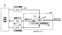
温度変化によりLD106の波長が変化すると、光増幅モジュール10の増幅特性に影響するため、一般的に励起用のLD106の温度は一定の温度に制御されている。図2はLD106の温度制御の構成例を示す。LD素子125に近接して配置されたサーミスタ(温度センサ)122でLD素子125の温度をモニタし、LD素子125の温度が一定となるように温度調整素子であるペルチェ素子120への注入電流量を制御する。温度センサ122の出力は温度モニタとしてのADC108でディジタル変換されて演算/制御回路30に入力され、ドライバ121による注入電流量が制御される。
When the wavelength of the
なお、複数のLD素子と、その各々に対応する複数のPD及び複数のサーミスタを単一の電子冷却素子上に実装する構成が提案されている(たとえば、特許文献1参照)。 A configuration in which a plurality of LD elements, a plurality of PDs corresponding to each of the LD elements, and a plurality of thermistors are mounted on a single electronic cooling element has been proposed (see, for example, Patent Document 1).
ペルチェ素子120への電流量が大きくなるほど温度を変化させる能力が高くなり、電流を流す向きを変えることで昇温、降温を制御する。励起用のLD106にとって、光を出力するためにLD素子125に注入する電流と、温度を一定にするためにペルチェ素子120に注入する電流の2つが必要となり、いずれも発熱の要因となる。
As the amount of current to the
最近の伝送ネットワークの複雑化に伴う光伝送装置の複雑化により、多数の光増幅器をアレイ状に配置して用いる構成も想定され、温度制御のための駆動電流と発熱量の増大が懸念される。 Due to the complication of optical transmission equipment accompanying the recent complication of transmission networks, it is also assumed that a large number of optical amplifiers are arranged in an array, and there is a concern about an increase in drive current and heat generation for temperature control. .
そこで、複数の光増幅器が配列される場合に温度制御に必要な駆動電流の増大を防止することのできる構成と、これを用いた光伝送装置を提供することを課題とする。 Accordingly, it is an object of the present invention to provide a configuration capable of preventing an increase in drive current necessary for temperature control when a plurality of optical amplifiers are arranged, and an optical transmission device using the configuration.
ひとつの態様では、光増幅器アレイは、
第1温度に制御される第1の励起光源を有する少なくとも1つの第1増幅部と、
前記第1温度と異なる第2温度に制御される第2の励起光源を有する少なくとも1つの第2増幅部と、
前記第1増幅部と前記第2増幅部に接続される制御回路と、
を有する。
In one aspect, the optical amplifier array comprises:
At least one first amplification unit having a first excitation light source controlled to a first temperature;
At least one second amplifying unit having a second excitation light source controlled to a second temperature different from the first temperature;
A control circuit connected to the first amplifying unit and the second amplifying unit;
Have
複数の光増幅器が配列される場合に、温度制御のための駆動電流の増大を防止することができる。 When a plurality of optical amplifiers are arranged, an increase in drive current for temperature control can be prevented.
複数の光増幅器を用いる場合、励起用のLDの制御温度と周囲温度との差が大きくなるほど、ペルチェ素子に供給する電流量は大きくなる。発明者は、制御温度の異なる、すなわち特定の波長光を出力させる温度が異なる2種類以上の励起レーザを用いることで、使用温度範囲にわたってペルチェ素子の制御に必要な駆動電流の最大値を低く抑えることができる構成に思い至った。以下の実施形態で、光増幅器アレイの好ましい構成例を説明する。 When a plurality of optical amplifiers are used, the amount of current supplied to the Peltier element increases as the difference between the control temperature of the excitation LD and the ambient temperature increases. The inventor suppresses the maximum value of the drive current necessary for controlling the Peltier element over the operating temperature range by using two or more types of excitation lasers having different control temperatures, that is, different temperatures for outputting specific wavelength light. I came up with a configuration that could do that. In the following embodiment, a preferred configuration example of the optical amplifier array will be described.
図3は、実施形態の構成に至る過程で考えられ得る構成を示す図である。光伝送装置1は、一例として、図の左側の伝送路と右側の伝送路の間で光信号を中継するが、図示の便宜上、左側の伝送路から右側の伝送路への伝送ルートについて接続構成を説明する。光伝送装置1は、伝送路から入力される光信号を増幅する光増幅器(プリアンプ)13−1と、伝送路へ出力される光信号を増幅する光増幅器(ポストアンプ)13−2と、アド(Add)側で任意の波長の信号を挿入する波長選択スイッチ(WSS)14addと、ドロップ(Drop)側で任意の波長の信号を分岐する波長選択スイッチ(WSS)14dropを有する(以下、適宜「WSS14」と総称する)。光伝送装置1は、右側の伝送路から左側の伝送路への伝送ルートについても、光増幅器(プリアンプ)12−1、光増幅器(ポストアンプ)12−2、波長選択スイッチ(WSS)11add、及び波長選択スイッチ(WSS)11drop(以下、適宜「WSS11」と総称する)を有する。WSS11dropで任意の波長の信号が分岐されて受信機側に送られる。WSS11addで送信機側からの任意の波長の信号が挿入されて伝送路に出力される。光伝送装置1は、同一信号を複数のポートに振り分けるマルチキャストスイッチ(MCS)15を有してもよい。また、ドロップ側でWSS11dropとWSS14dropに替えて光カプラや光セレクタを用いてもよい。アド側でWSS11addとWSS14addに替えて光りカプラを用いてもよい。
FIG. 3 is a diagram illustrating a configuration that can be considered in the process leading to the configuration of the embodiment. As an example, the
WSS11、14やMCS15は光損失が大きいので、光レベルの低下を補償するために、アド側のポートP5〜P8、ドロップ側のポートP1〜P4の各々に光増幅モジュール10を配置して所望の光レベルを得ることが考えられる。
Since WSS11, 14 and MCS15 have a large optical loss, an
しかし、図3のように、多数あるポートの各々に光増幅モジュール10を搭載する構成は、物理的に実現が困難である。そこで、図4及び図5に示すように、演算/制御回路30を共通に使用して複数の増幅部20をひとつの筐体に収容あるいは一つの基板上に搭載するアレイ型の増幅器50(以降、「増幅器アレイ50」と称する)を使用することが考えられる。
However, as shown in FIG. 3, the configuration in which the
図4の例では、MCS15と、WSS14及びWSS11の間に、アド側ポートP5〜P8及びドロップ側ポートP1〜P4のすべてに共通に用いられる光増幅器アレイ50が挿入されている。図示の便宜上、WSS11とアレイ型光増幅器50及びMCS15との間の接続線は省略されている。図5に示すように、光増幅器アレイ50で用いられる複数の増幅部20は、各ポートで挿入、分岐される光信号を増幅するためのものであり、光伝送装置1と伝送路の間の送受信で用いられる光増幅器12−1、12−2、13−1、及び13−2とは区別される。
In the example of FIG. 4, an
図5は、光伝送装置1に光増幅器アレイ50を用いる場合、一般的に考えられる構成例を示す。アド側とドロップ側の各ポートに対応して複数の増幅部20が配置される。図示の便宜上、詳細な構成は省略されているが、複数の増幅部20は同じ構成を有し、その基本構成は図1の増幅部20と同様である。各増幅部20で、入射側のPD102のモニタ出力と、EDF109の後段に配置される出力側のPD112のモニタ出力が、共通の演算/制御回路30に入力される。
FIG. 5 shows a configuration example that can be generally considered when the
各増幅部20は、励起光源としてLD106を有する。励起用のLDには、980nm帯のLDと、1480nm帯のLDの2種類がある。一般的には、増幅時の自然放出光(ASE:Amplified Spontaneous Emission)による雑音の発生が少なく、かつコストの低い980nm帯のLDが使われている。半導体LDは、温度の変化により素子内部の屈折率が変化することで発振波長が変化する。発信波長の変化と同時に、量子効率(注入電流を光出力に変換する割合)が変化し、光出力が変化する。一般的に温度が高くなると波長は長波長側にシフトし、出力は低下する方向に変化する。
Each
図5の例では、励起用のLD106、EDF109、入力モニタ用のPD102、出力モニタ用のPD112を含む増幅部20が8セット搭載されている。LD106は、図2に示すようにLD素子125と温度制御素子(ペルチェ素子)120を有している。アレイ構成として、ひとつの増幅部20の8倍のサイズ(体積)を有する構成が求められるわけではなく、単純に乗算した体積よりも小さい体積内に収容する構成が求められる。その場合、より小さい体積内で複数(たとえば8個)のLD106からの発熱を考慮しなければならない。
In the example of FIG. 5, eight sets of amplifying
図6は、複数のLD106を単純に並べたときに生じ得る課題を説明する図である。一般的に励起用のLD106は、発振波長を一定にするために25℃の温度を保つように制御されている。周囲温度が高くなると、LD106の温度を下げるために、ペルチェ素子120(図2参照)でより多くの電流量を消費し、周囲温度が低くなると、LD106の温度を上げて25℃にするためにペルチェ素子120でより多くの電流が消費される。
FIG. 6 is a diagram for explaining a problem that may occur when a plurality of
図6に示すように、周囲温度が25℃であれば、ペルチェ素子120に電流を流す必要がなく、温度制御のための電流量はゼロとなるが、LD106の制御温度と周囲温度との差が大きくなるにつれて、ペルチェ素子120に供給すべき電流量が増大する。周囲環境が高温の時や低温の時には、各LD106での消費電力、よく具体的にはペルチェ素子120へ供給する電流量が大きくなる。8個のLD106を単純に並べると、周囲の温度変化につれて、ペルチェ素子120(図2参照)に供給すべき電流量が8倍になり、光増幅器アレイ50全体での消費電力の増大がより顕著となる。この場合、大きな電流量を確保するために大容量の電流源が必要になるばかりでなく、ペルチェ素子120に供給する電流による発熱量も増大する。
As shown in FIG. 6, when the ambient temperature is 25 ° C., it is not necessary to pass a current through the
そこで、以下の実施形態で、複数の増幅器を用いる光増幅器アレイにおいて、アレイ全体として消費電力の増大を抑制することのできる構成を提供する。
<第1実施形態>
図7は、第1実施形態の光増幅器アレイ50Aの配置構成を示す。図7の光増幅器アレイ50Aは、異なる温度に制御される2種類のLD106AとLD106Bを交互に配置する。LD106Aの励起用のLD素子125(図2参照)は、たとえば25℃の一定温度に制御される。LD106Bの励起用のLD素子125は、たとえば45℃の一定温度に制御される。LD素子125の温度制御を行うことで、周囲の環境温度の変化により発振特性が変化することを防ぐ。光増幅器アレイ50の内部では、LD106自体からの発熱や、演算/制御回路30やその他の電気・電子部品からの発熱により、周囲温度が45℃を超えて高温になる場合が多い。他方、使用場所や季節によっては、周囲温度が25℃よりも低い温度になる場合もある。後述するように、25℃に制御されるLD106Aと45℃に制御されるLD106Bを混合して搭載することで、特に周囲温度が制御温度から離れた領域で温度制御のための電流供給量の増加を抑制することができる。その結果、光増幅器アレイ全体での消費電力の増大を抑制することができる。
Therefore, in the following embodiment, a configuration is provided that can suppress an increase in power consumption as an entire array in an optical amplifier array using a plurality of amplifiers.
<First Embodiment>
FIG. 7 shows an arrangement configuration of the
図8は、光増幅器アレイ50の消費電力増大の抑制を説明する図である。図8(A)において、25℃制御のLD106Aのペルチェ電流を破線で示し、45℃制御のLD106Bのペルチェ電流を実線で示し、モジュール全体のペルチェ電流を太線で示す。25℃制御のLD106Aでは、25℃を境に周囲温度が低くなっても高くなってもペルチェ電流が増大する。45℃制御のLD106Bでは、45℃を境に周囲温度が低くなっても高くなってもペルチェ電流量が増大する。異なる制御温度のLD106AとLD106Bを混載することで、制御温度から離れた高温領域と低温領域でペルチェ電流量の増大を抑制することができる。換言すると、ペルチェ素子120に供給されるトータルの駆動電流量の最大値を低く抑え、環境温度全体にわたってペルチェ電流量を分散化して電流量の増大を抑制する。
FIG. 8 is a diagram for explaining suppression of increase in power consumption of the
図8(B)に示すように、25℃制御のLD106Aは、周囲温度が55℃〜70℃の高温領域でペルチェ電流が最も大きくなり、45℃制御のLD106Bは、周囲温度が0℃〜15度の低温領域でペルチェ電流が最も大きくなる。モジュールあるいは光増幅器アレイ50全体では、図8(A)に示すように、周囲温度が25℃〜45℃の間でペルチェ電流量がほぼ一定量であり、周囲温度が45℃よりも高くなる場合や25℃よりも低くなる場合は、ペルチェ電流の変化の割合(傾き)が緩やかである。中温域のペルチェ電流が平均化されるとともに、制御温度から離れる低温領域、高温領域での極端な電流増加が抑制される。一般に、光伝送装置1の使用時は増幅器アレイ50の内部温度は高温になりやすく、図6と比較して、特に高温時の消費電力の抑制効果が期待できる。
As shown in FIG. 8B, the
図7に戻って、25℃制御のLD106Aと45℃制御のLD106Bを交互に配置することで、各LD106でのペルチェ素子120からの発熱量を分散化し平均化することができる。
<第2実施形態>
第1実施形態では、アド側、ドロップ側に関係なく、隣接するポートで制御温度の異なるLD106AとLD106Bを使用する例を示した。現実的には、アド側、ドロップ側で実現すべき光特性(入力レベル、出力レベル)が異なるため、使用する励起用のLD素子125に求められる出力パワーが異なる可能性が高い。そこで第2実施形態では、アド側のポートとドロップ側のポートを交互に配置して、互いに隣接する異なる機能のポートに制御温度の異なるLD106を配置する。この構成は、LD106の温度制御に必要なペルチェ電流の最大値を低く抑えるとともに、ペルチェ素子120からの発熱を分散させて光特性への影響を低減することができる。
Returning to FIG. 7, by disposing the
Second Embodiment
In the first embodiment, the example in which the
図9は、第2実施形態の光増幅器アレイ50Bの配置構成を示す。図9の光増幅器アレイ50Bでは、アド側のポートに挿入される増幅部20Bと、ドロップ側のポートに挿入される増幅部20Aが交互に配置される。アド側の増幅部20Bには、各送信機(Tx)からの光信号が入力され、ドロップ側の増幅部20Aの出力は各受信機(Rx)に供給される(図4参照)。
FIG. 9 shows an arrangement configuration of the optical amplifier array 50B of the second embodiment. In the optical amplifier array 50B of FIG. 9, the
一例として、ドロップ側の増幅部20Aでは、25℃に温度制御されるLD106Aが使用され、アド側の増幅部20Bでは、45℃に温度制御されるLD106Bが配置される。一般に、送信側は大きな光出力を必要とし、増幅部20Bの温度も高くなりやすいので、45℃で供給すべきペルチェ電流が最小となるLD106Bを用いる。受信側は、伝送路を伝搬してきた光信号を受け取るため、最適なゲインを得るために入力信号光をLD106AとEDF109で増幅するが、送信側ほど大きな励起エネルギーを用いなくてもよい。そこで、25℃で供給すべきペルチェ電流が最小となるLD106Aを用いる。
As an example, an
機能ごとに異なる制御温度のLD106A、106Bを配置することで、図8で説明したのと同様に、ペルチェ素子120を駆動するための最大電流量を低く抑えて、光増幅器アレイ50B全体での消費電力と発熱量の増大を抑制することができる。また、光特性への影響を低減することができる。
<適用例>
図10及び図11は、実施形態の光増幅器アレイ50をひとつのモジュール内にパッケージ化したアレイ型光増幅器モジュール5への適用例を示す。複数の増幅部20をひとつのモジュール内に配置する場合、発熱量と消費電力の増大の抑制はさらに望まれる。図10と図11において、光増幅器アレイ50は、第1実施形態の光増幅器アレイ50Aであってもよいし、第2実施形態の光増幅器アレイ50Bであってもよい。
By arranging the
<Application example>
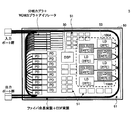
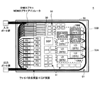
10 and 11 show an application example to the array type
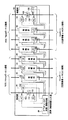
図10及び図11において、同じ種類の部品はプリント板61上の同じ領域に配置されている。光部品であるPD(入力モニタ用のPDと出力モニタ用のPDを含む)のグループはある領域に配置され、分岐カプラ、EDMカプラ、及びアイソレータは、PDの配置領域に隣接して配置されている。また、DSP30やその他の電気・電子部品51もそれぞれの領域に配置され、プリント板61の外周に沿って、光ファイバの余長部分とEDFが実装されている。
10 and 11, the same type of components are arranged in the same region on the printed
図10の構成例では、LD配置領域53に、異なる制御温度を有するLD106AとLD106Bが交互に配置されている。同じ制御温度のLDを分散配置することで、発熱を分散させ、アレイ型光増幅器モジュール5全体としての消費電力の増大を抑制する。
In the configuration example of FIG. 10,
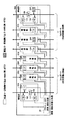
図11の構成例では、第1の制御温度(たとえば25℃)を有するLD106AをLD配置領域53Aにまとめて配置し、第2の制御温度(たとえば45℃)を有するLD106BをLD配置領域53Bに配置する。この配置は、アレイ型光増幅器モジュール5の内部構成や他の部品配置の関係から、アレイ型光増幅器モジュール5の内部で温度差が出やすい場合に有効である。
In the configuration example of FIG. 11, the
設計時に実施する熱シミュレーションから、アレイ型光増幅器モジュール5の内部部品の配置・搭載構成や、熱引きの良し悪しなどの熱環境の違いをあらかじめ知ることができる。高温になりやすい場所にLD配置領域53Bを設定し、高い温度に制御される励起用のLD(たとえば45℃に制御されるLD106B)を配置する。LD配置領域53Bと比較して高温になりにくい場所にLD配置領域53Aを設定して、低い温度に制御される励起用のLD(たとえば25℃に制御されるLD106A)を配置する。
From the thermal simulation performed at the time of design, it is possible to know in advance the differences in the thermal environment such as the arrangement / mounting configuration of the internal components of the array type
この構成により、各LDの制御温度と周囲温度の差をなるべく小さくして、アレイ型光増幅器モジュール5全体の消費電力の増大を抑制することができる。
With this configuration, the difference between the control temperature of each LD and the ambient temperature can be made as small as possible, and an increase in power consumption of the entire array
上述の実施形態及び適用例では、制御温度の異なる2種類の励起用のLD106AとLD106Bを用いる例を示したが、3種類以上の励起用のLDを使用する場合も同様の効果を得ることができる。
In the above-described embodiments and application examples, two types of
励起用のLDでは、一定温度に制御されるタイプ以外に、温度制御不要のものがある。温度制御不要のLDでは、温度変化によるLD素子125の特性(主に光出力)の変化率が小さい素子を使用するが、LD素子125自体の性能として大きな出力は出せないという特徴がある。このため、任意の波長の信号をアドまたはドロップする光伝送装置1においては、光増幅による大きな出力の必要なアド側に温度制御不要の励起用のLDを適用することができない。そこで、アド側に温度制御を行うタイプの励起用のLD106を使用し、光増幅後の光出力がアド側ほど高くなくてもよいドロップ側に、温度制御不要の励起用のLDを使用してもよい。この場合、温度制御するタイプの励起用のLDと、温度制御不要の励起用LDを図10のように分散配置することで、温度制御用の電流供給量を半分にして、アレイ型光増幅器モジュール5全体としての消費電力の増大を抑制するとともに発熱を分散することができる。
Some types of excitation LDs do not require temperature control other than the type controlled at a constant temperature. An LD that does not require temperature control uses an element that has a small rate of change in the characteristics (mainly light output) of the
また、光増幅器アレイに、第1温度(たとえば25℃)に制御される励起LDを用いる第1増幅部と、第2温度(たとえば45℃)に制御される励起LDを用いる第2増幅部と、温度制御不要な励起LDを用いる第3増幅部を搭載してもよい。第1増幅部〜第3増幅部は、交互に配置してもよいし、パッケージ内の他の部品の配置状況や熱分布に応じて分散配置してもよい。この場合も、アレイ全体で温度制御用の電流の最大供給量を抑制して消費電力の増大を防止することができる。 In addition, a first amplifier using an excitation LD controlled to a first temperature (for example, 25 ° C.) and a second amplifier using an excitation LD controlled to a second temperature (for example, 45 ° C.) for the optical amplifier array A third amplifying unit using an excitation LD that does not require temperature control may be mounted. The first amplifying unit to the third amplifying unit may be arranged alternately, or may be arranged in a distributed manner according to the arrangement status of other components in the package and the heat distribution. In this case as well, the maximum supply amount of the current for temperature control can be suppressed in the entire array to prevent the increase in power consumption.
1 光伝送装置
5 アレイ型光増幅器モジュール
10 光増幅モジュール
11add、14add 波長選択スイッチ(アド側)
11drop、14drop 波長選択スイッチ(ドロップ側)
12−1,13−1 光増幅器(プリアンプ)
12−2、13−2 光増幅器(ポストアンプ)
20 増幅部
20A 増幅部(第1増幅部)
20B 増幅部(第2増幅部)
30 演算/制御回路
50、50A、50B 光増幅器アレイ
53 LD配置領域
53A 第1のLD配置領域
53B 第2のLD配置領域
106 LD(励起光源)
106A LD(第1の励起光源)
106B LD(第2の励起光源)
120 ペルチェ素子(温度制御素子)
122 温度センサ
125 LD素子
161 プリント板
P1〜P4 ドロップ側ポート
P5〜P8 アド側ポート
DESCRIPTION OF
11drop, 14drop wavelength selective switch (drop side)
12-1, 13-1 Optical amplifier (preamplifier)
12-2, 13-2 Optical amplifier (post-amplifier)
20
20B Amplification unit (second amplification unit)
30 Arithmetic /
106A LD (first excitation light source)
106B LD (second excitation light source)
120 Peltier element (temperature control element)
122
Claims (5)
前記第1温度と異なる第2温度に制御される第2の励起光源を有する少なくとも1つの第2増幅部と、
前記第1増幅部と前記第2増幅部に接続される制御回路と、
を有し、
前記第1増幅部と前記第2増幅部は、交互に配置されることを特徴とする光増幅器アレイ。 At least one first amplification unit having a first excitation light source controlled to a first temperature;
At least one second amplifying unit having a second excitation light source controlled to a second temperature different from the first temperature;
A control circuit connected to the first amplifying unit and the second amplifying unit;
I have a,
Wherein the second amplifier and the first amplifying unit, the optical amplifier array to feature to be arranged alternately.
前記第1温度と異なる第2温度に制御される第2の励起光源を有する少なくとも1つの第2増幅部と、 At least one second amplifying unit having a second excitation light source controlled to a second temperature different from the first temperature;
前記第1増幅部と前記第2増幅部に接続される制御回路と、 A control circuit connected to the first amplifying unit and the second amplifying unit;
を有し、Have
前記第1の励起光源は、基板上の第1領域内に配置され、 The first excitation light source is disposed in a first region on the substrate;
前記第2の励起光源は、前記基板上の前記第1領域と異なる熱分布を有する第2領域内に配置されていることを特徴とする光増幅器アレイ。 The optical amplifier array, wherein the second excitation light source is disposed in a second region having a heat distribution different from that of the first region on the substrate.
前記第2増幅部に配置されて前記第2の励起光源の動作温度を制御する第2の温度制御素子と、
をさらに有することを特徴とする請求項1または2に記載の光増幅器アレイ。 A first temperature control element disposed in the first amplifying unit for controlling an operating temperature of the first excitation light source;
A second temperature control element disposed in the second amplifying unit for controlling an operating temperature of the second excitation light source;
Optical amplifier array of claim 1 or 2, characterized in that it further comprises a.
前記光増幅器アレイに接続される波長選択スイッチと、
を有することを特徴とする光伝送装置。 An optical amplifier array according to any one of claims 1 to 4 ,
A wavelength selective switch connected to the optical amplifier array;
An optical transmission device comprising:
Priority Applications (2)
| Application Number | Priority Date | Filing Date | Title |
|---|---|---|---|
| JP2015008749A JP6476894B2 (en) | 2015-01-20 | 2015-01-20 | Optical amplifier array and optical transmission device using the same |
| US14/953,872 US9614345B2 (en) | 2015-01-20 | 2015-11-30 | Arrayed optical amplifier and optical transmission device |
Applications Claiming Priority (1)
| Application Number | Priority Date | Filing Date | Title |
|---|---|---|---|
| JP2015008749A JP6476894B2 (en) | 2015-01-20 | 2015-01-20 | Optical amplifier array and optical transmission device using the same |
Publications (2)
| Publication Number | Publication Date |
|---|---|
| JP2016134796A JP2016134796A (en) | 2016-07-25 |
| JP6476894B2 true JP6476894B2 (en) | 2019-03-06 |
Family
ID=56408529
Family Applications (1)
| Application Number | Title | Priority Date | Filing Date |
|---|---|---|---|
| JP2015008749A Expired - Fee Related JP6476894B2 (en) | 2015-01-20 | 2015-01-20 | Optical amplifier array and optical transmission device using the same |
Country Status (2)
| Country | Link |
|---|---|
| US (1) | US9614345B2 (en) |
| JP (1) | JP6476894B2 (en) |
Families Citing this family (1)
| Publication number | Priority date | Publication date | Assignee | Title |
|---|---|---|---|---|
| JP6879364B2 (en) * | 2016-09-20 | 2021-06-02 | 日本電気株式会社 | Optical amplifier and control method of optical amplifier |
Family Cites Families (19)
| Publication number | Priority date | Publication date | Assignee | Title |
|---|---|---|---|---|
| JP3266165B2 (en) * | 1993-05-13 | 2002-03-18 | 住友電気工業株式会社 | Optical fiber amplifier |
| SE506748C2 (en) * | 1995-06-26 | 1998-02-09 | Ericsson Telefon Ab L M | Method and apparatus for removing and adding channels in an optical multiplexer |
| US6441955B1 (en) * | 1998-02-27 | 2002-08-27 | Fujitsu Limited | Light wavelength-multiplexing systems |
| JP2000031575A (en) | 1998-07-09 | 2000-01-28 | Oki Electric Ind Co Ltd | Ld module |
| WO2001084679A1 (en) * | 2000-04-29 | 2001-11-08 | Corning Incorporated | Universal controller for an optical amplifier |
| US6570704B2 (en) * | 2001-03-14 | 2003-05-27 | Northrop Grumman Corporation | High average power chirped pulse fiber amplifier array |
| US6633599B2 (en) * | 2001-08-01 | 2003-10-14 | Lite Cycles, Inc. | Erbium-doped fiber amplifier pump array |
| JP2004064031A (en) * | 2002-06-03 | 2004-02-26 | Mitsubishi Cable Ind Ltd | Optical amplifier and light source device |
| JP4301822B2 (en) * | 2003-01-24 | 2009-07-22 | 富士通株式会社 | Optical amplifier with polarization mode dispersion compensation function |
| JP2005026558A (en) * | 2003-07-04 | 2005-01-27 | Furukawa Electric Co Ltd:The | Optical amplifier and optical transmission system using the same |
| DE102006010147A1 (en) * | 2006-03-06 | 2007-09-13 | Siemens Ag | Bidirectional optical amplifier arrangement |
| WO2008125142A1 (en) * | 2007-04-13 | 2008-10-23 | Telefonaktiebolaget Lm Ericsson (Publ) | Optical signal amplifier, method of optical amplification and optical network |
| JP2009003378A (en) * | 2007-06-25 | 2009-01-08 | Fujitsu Ltd | Mirror device and optical switch |
| JP5121687B2 (en) * | 2008-12-16 | 2013-01-16 | 株式会社日立製作所 | Optical branch multiplexing system and optical branch multiplexing apparatus |
| US8447183B2 (en) * | 2009-04-24 | 2013-05-21 | Tellabs Operations, Inc. | Methods and apparatus for performing directionless and contentionless wavelength addition and subtraction |
| JP6070101B2 (en) * | 2012-11-19 | 2017-02-01 | 富士通株式会社 | Optical amplification apparatus and transmission system |
| US8995484B2 (en) * | 2013-02-22 | 2015-03-31 | Applied Optoelectronics, Inc. | Temperature controlled multi-channel transmitter optical subassembly and optical transceiver module including same |
| US9455782B2 (en) * | 2014-08-11 | 2016-09-27 | Applied Optoelectronics, Inc. | Monitoring a multiplexed laser array in an optical communication system |
| US9368941B1 (en) * | 2014-08-14 | 2016-06-14 | Google Inc. | Temperature compensation in an optical transmitter |
-
2015
- 2015-01-20 JP JP2015008749A patent/JP6476894B2/en not_active Expired - Fee Related
- 2015-11-30 US US14/953,872 patent/US9614345B2/en not_active Expired - Fee Related
Also Published As
| Publication number | Publication date |
|---|---|
| US9614345B2 (en) | 2017-04-04 |
| US20160211641A1 (en) | 2016-07-21 |
| JP2016134796A (en) | 2016-07-25 |
Similar Documents
| Publication | Publication Date | Title |
|---|---|---|
| JP6233100B2 (en) | Optical amplification repeater and optical transmission station | |
| JP3854673B2 (en) | Optical amplification medium control method, optical amplification device, and system using the same | |
| US8774624B2 (en) | Optical transmission apparatus and optical communication system | |
| US6606188B2 (en) | Optical repeater using raman amplification, wavelength division multiplexed light transmission system, excitation light supply method and excitation light control method for raman amplification | |
| JP2008294462A (en) | Low-power laser driver | |
| JPH08278523A (en) | Optical amplifier | |
| US8873972B2 (en) | Optical transmission apparatus and optical transmission system | |
| US20140285874A1 (en) | Method for controlling signal gain of a raman amplifier | |
| JP2010010987A (en) | Optical transmission system using raman optical amplification | |
| JP6476894B2 (en) | Optical amplifier array and optical transmission device using the same | |
| JP6070101B2 (en) | Optical amplification apparatus and transmission system | |
| JP2001036169A (en) | Bidirectional pump light amplifier | |
| US7324268B2 (en) | Optical signal amplifier and method | |
| US6707599B1 (en) | Optical network equipment with triggered data storage | |
| KR20110052496A (en) | ARC Coated Quantum Dot Resonator for Wavelength Division Multiplexing Optical Communication | |
| JP2003202422A (en) | Optical attenuation module, optical amplifier and pump light source using the same | |
| US9654215B2 (en) | Modular kit of the spectrally flexible device for bidirectional transmissions of optical signals sensitive to timing in the internet and other networks | |
| JP2003273462A (en) | Semiconductor laser module, fiber type optical amplifier, optical repeater, and optical transmission system | |
| JPWO2019187051A1 (en) | Optical amplifier, control method of optical amplifier and optical communication system | |
| JP6103159B1 (en) | Optical amplifier | |
| JP3933514B2 (en) | Optical amplifier and optical communication system using the optical amplifier | |
| JP2006286844A (en) | Optical fiber amplifier | |
| JP4032804B2 (en) | Optical amplifier and output control method thereof | |
| JP5967737B1 (en) | Optical communication system and multimode optical fiber amplifier | |
| JP2001060917A (en) | WDM optical transmitter and optical amplifier |
Legal Events
| Date | Code | Title | Description |
|---|---|---|---|
| A621 | Written request for application examination |
Free format text: JAPANESE INTERMEDIATE CODE: A621 Effective date: 20171113 |
|
| A131 | Notification of reasons for refusal |
Free format text: JAPANESE INTERMEDIATE CODE: A131 Effective date: 20180814 |
|
| A521 | Request for written amendment filed |
Free format text: JAPANESE INTERMEDIATE CODE: A523 Effective date: 20181004 |
|
| TRDD | Decision of grant or rejection written | ||
| A01 | Written decision to grant a patent or to grant a registration (utility model) |
Free format text: JAPANESE INTERMEDIATE CODE: A01 Effective date: 20190108 |
|
| A61 | First payment of annual fees (during grant procedure) |
Free format text: JAPANESE INTERMEDIATE CODE: A61 Effective date: 20190121 |
|
| R150 | Certificate of patent or registration of utility model |
Ref document number: 6476894 Country of ref document: JP Free format text: JAPANESE INTERMEDIATE CODE: R150 |
|
| LAPS | Cancellation because of no payment of annual fees |