JP6468747B2 - Developer container, developing device, process cartridge, and image forming apparatus - Google Patents
Developer container, developing device, process cartridge, and image forming apparatus Download PDFInfo
- Publication number
- JP6468747B2 JP6468747B2 JP2014152906A JP2014152906A JP6468747B2 JP 6468747 B2 JP6468747 B2 JP 6468747B2 JP 2014152906 A JP2014152906 A JP 2014152906A JP 2014152906 A JP2014152906 A JP 2014152906A JP 6468747 B2 JP6468747 B2 JP 6468747B2
- Authority
- JP
- Japan
- Prior art keywords
- developer
- conductive path
- frame
- conductive resin
- developing
- Prior art date
- Legal status (The legal status is an assumption and is not a legal conclusion. Google has not performed a legal analysis and makes no representation as to the accuracy of the status listed.)
- Active
Links
Images


Classifications
-
- G—PHYSICS
- G03—PHOTOGRAPHY; CINEMATOGRAPHY; ANALOGOUS TECHNIQUES USING WAVES OTHER THAN OPTICAL WAVES; ELECTROGRAPHY; HOLOGRAPHY
- G03G—ELECTROGRAPHY; ELECTROPHOTOGRAPHY; MAGNETOGRAPHY
- G03G15/00—Apparatus for electrographic processes using a charge pattern
- G03G15/06—Apparatus for electrographic processes using a charge pattern for developing
- G03G15/08—Apparatus for electrographic processes using a charge pattern for developing using a solid developer, e.g. powder developer
- G03G15/0822—Arrangements for preparing, mixing, supplying or dispensing developer
- G03G15/0848—Arrangements for testing or measuring developer properties or quality, e.g. charge, size, flowability
- G03G15/0856—Detection or control means for the developer level
- G03G15/086—Detection or control means for the developer level the level being measured by electro-magnetic means
-
- G—PHYSICS
- G03—PHOTOGRAPHY; CINEMATOGRAPHY; ANALOGOUS TECHNIQUES USING WAVES OTHER THAN OPTICAL WAVES; ELECTROGRAPHY; HOLOGRAPHY
- G03G—ELECTROGRAPHY; ELECTROPHOTOGRAPHY; MAGNETOGRAPHY
- G03G15/00—Apparatus for electrographic processes using a charge pattern
- G03G15/80—Details relating to power supplies, circuits boards, electrical connections
Landscapes
- Physics & Mathematics (AREA)
- General Physics & Mathematics (AREA)
- Dry Development In Electrophotography (AREA)
- Electrophotography Configuration And Component (AREA)
Description
本発明は、複写機、プリンタ、ファクシミリ装置などの画像形成装置、およびこの画像形成装置にて用いられる現像剤容器、現像装置、プロセスカートリッジに関するものである。 The present invention relates to an image forming apparatus such as a copying machine, a printer, and a facsimile machine, and a developer container, a developing apparatus, and a process cartridge used in the image forming apparatus.
従来、電子写真方式を採用する画像形成装置には、像坦持体に走査露光することにより形成された静電潜像に現像剤を供給する事で現像剤像を形成する現像装置が設けられている。近年では、現像装置が像担持体とその他のプロセス手段(帯電部材等)と共にプロセスカートリッジとして一体に収容されている場合が多い。このようにプロセスカートリッジとして一体化し、さらにプロセスカートリッジを画像形成装置の装置本体に対して着脱可能とすることにより、現像剤の補給やメンテナンス作業を容易に行うことができる。 2. Description of the Related Art Conventionally, an image forming apparatus employing an electrophotographic system is provided with a developing device that forms a developer image by supplying a developer to an electrostatic latent image formed by scanning exposure on an image carrier. ing. In recent years, a developing device is often housed as a process cartridge together with an image carrier and other process means (such as a charging member). By integrating the process cartridge as described above and making the process cartridge detachable from the apparatus main body of the image forming apparatus, it is possible to easily supply the developer and perform maintenance work.
このようなプロセスカートリッジ方式では、現像剤が無くなった時点で、ユーザーがカートリッジを交換し、現像剤を補充することで、再び画像を形成することができる。そのため、このような画像形成装置は、現像剤が消費された場合にそれを検知し、ユーザーに交換時期を報知する手段、即ち、現像剤残量検知手段を備えているものが一般的である。 In such a process cartridge system, when the developer runs out, the user can replace the cartridge and replenish the developer to form an image again. Therefore, such an image forming apparatus is generally provided with a means for detecting when the developer is consumed and notifying the user of the replacement time, that is, a developer remaining amount detecting means. .
このような現像剤残量検知手段として特許文献1には、一対の入力側および出力側電極を備え、両電極間の静電容量を測定することによって現像剤量を検出するプレートアンテナ方式が提案されている。 As such a developer remaining amount detecting means, Patent Document 1 proposes a plate antenna system that includes a pair of input and output electrodes and detects the developer amount by measuring the capacitance between both electrodes. Has been.
また、特許文献2には現像剤担持体に交流バイアスを印加する事で、現像剤担持体を入力側電極と見なし、出力側電極となる静電容量検知部材を現像装置内の現像剤担持体に対向する箇所に設ける構成が提案されている。
Further, in
この静電容量検知部材と現像剤担持体との間の静電容量は、絶縁性トナーなどの現像剤量に応じて変化することを利用したものである。即ち、この静電容量検知部材と現像剤担持体との間の空間が現像剤で埋まっていれば、その間の静電容量は大きくなり、現像剤が減るにつれて両者の間の空間を空気が占める率が増え、静電容量は小さくなっていく。従って、静電容量検知部材である板金と現像剤担持体との間の静電容量、或いは板金間の静電容量と現像剤量の関係を予め求めておけば、静電容量を測定することによって使用中の現像装置の現在の現像剤量を検知することができる。 The electrostatic capacity between the electrostatic capacity detection member and the developer carrying member is used to change according to the amount of developer such as insulating toner. That is, if the space between the electrostatic capacity detection member and the developer carrying member is filled with the developer, the electrostatic capacity therebetween increases, and air occupies the space between the two as the developer decreases. The rate increases and the capacitance decreases. Therefore, if the capacitance between the sheet metal as the capacitance detection member and the developer carrier or the relationship between the capacitance between the sheet metal and the developer amount is obtained in advance, the capacitance is measured. The current developer amount of the developing device in use can be detected.
さらに、特許文献3において、プレートアンテナを固定する方法として、アンテナ部材をカートリッジ枠体に両面テープで貼り付ける場合や、枠体に直接蒸着や印刷等の処理を施す構成が開示されている。加えて、枠体の樹脂と電極を形成する導電性樹脂とを2色成型する構成も開示されている。 Further, Patent Document 3 discloses a method for fixing a plate antenna, in which an antenna member is attached to a cartridge frame with a double-sided tape, or a configuration in which a process such as vapor deposition or printing is performed directly on the frame. In addition, a configuration in which the resin of the frame and the conductive resin forming the electrode are molded in two colors is also disclosed.
しかし、このような電極間の静電容量を測定することによって現像剤量を検出する方式においては、検出電極からの金属配線を設ける必要があるが、配線の配置が複雑化する傾向があった。 However, in such a method of detecting the developer amount by measuring the capacitance between the electrodes, it is necessary to provide a metal wiring from the detection electrode, but the wiring arrangement tends to be complicated. .
そこで、本発明は、現像剤を収容するための現像剤容器であって、現像剤を収容する枠体と、長手方向を有する形状をした電極と、前記長手方向に延び、前記枠体の前記現像剤を収容する内側に設けられ、前記電極との間にある前記現像剤の量に応じた電流の信号を出力する検出部材と、前記検出部材と繋がっており、且つ前記長手方向と交差する前記枠体の面で前記枠体の外側に露出する露出部を有し、前記露出部により前記検出部材に流れる電流の信号を前記枠体の外部に出力する、導電性樹脂で構成される導電樹脂部材と、を有し、前記枠体と前記導電樹脂部材とは一体成形されている現像剤容器を提供するものである。 Therefore, the present invention is a developer container for containing a developer, a frame containing the developer, an electrode having a longitudinal direction, and extending in the longitudinal direction, A detection member that is provided inside the developer and outputs a current signal corresponding to the amount of the developer between the electrode and the electrode, and is connected to the detection member and intersects the longitudinal direction. A conductive layer made of a conductive resin that has an exposed portion exposed to the outside of the frame body on the surface of the frame body and outputs a signal of a current flowing through the detection member to the outside of the frame body by the exposed portion. A developer container is provided, and the frame body and the conductive resin member are integrally molded.
さらに、本発明は、現像装置、プロセスカートリッジおよび画像形成装置を提供するものである。 Furthermore, the present invention provides a developing device, a process cartridge, and an image forming apparatus.
本発明によれば、導電経路に樹脂を用いることにより、構造を簡素化することができる。 According to the present invention, the structure can be simplified by using a resin for the conductive path.
(実施例1)
以下、現像剤残量検知手段を有する現像剤容器、現像装置、プロセスカートリッジ、および画像形成装置を図面に則して詳しく説明する。
Example 1
Hereinafter, a developer container having a developer remaining amount detecting means, a developing device, a process cartridge, and an image forming apparatus will be described in detail with reference to the drawings.
(1)画像形成装置とプロセスカートリッジの構成と動作の概略
図2は本実施例における画像形成装置の概略図である。この画像形成装置は、電子写真方式かつプロセスカートリッジ着脱式のレーザビームプリンタである。このプリンタにはパソコン・画像読取装置等の外部ホスト装置を接続する事で、画像情報を受け取りプリントする。
(1) Outline of Configuration and Operation of Image Forming Apparatus and Process Cartridge FIG. 2 is a schematic view of the image forming apparatus in this embodiment. This image forming apparatus is an electrophotographic and process cartridge detachable laser beam printer. By connecting an external host device such as a personal computer or an image reading device to the printer, image information is received and printed.
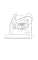
1はプリンタ本体(画像形成装置本体)、2はプリンタ本体1に対して着脱可能なプロセスカートリッジである。また、図3は実施例1におけるプロセスカートリッジの断面図であり、プロセスカートリッジ2についてはこれを用いて説明する。
Reference numeral 1 denotes a printer main body (image forming apparatus main body), and 2 denotes a process cartridge that can be attached to and detached from the printer main body 1. FIG. 3 is a cross-sectional view of the process cartridge according to the first embodiment, and the
図3において、20は像担持体としてのドラム型の電子写真感光体(以下、感光ドラムという。)である。本実施例では、感光ドラム20と、帯電装置30と、現像装置40と、クリーニング装置52の4種のプロセス装置を一体的にカートリッジ化し、プリンタ本体1に着脱可能としている。
In FIG. 3,
感光ドラム20はプリントスタート信号に基づいて矢印R1の時計方向に157.6mm/sの周速度(プロセススピード)をもって回転駆動される。本実施例では、帯電装置30としてローラ帯電方式を用いた。感光ドラム20には帯電バイアスが印加される帯電ローラ30を接触させてあり、帯電ローラ30は感光ドラム20に従動して回転駆動される。回転する感光ドラム20の周面がこの帯電装置30により所定の極性・電位に一様に帯電される。本実施例では負の所定電位に帯電される。
The
露光装置3はホスト装置からコントローラ部へ入力された画像情報の時系列電気デジタル画素信号に対応して変調(オン/オフ変換)されたレーザ光を出力して、帯電ローラ30によって一様に帯電された感光ドラム20のドラム面を走査露光する。本実施例では画像情報部を露光するイメージ露光方式である。
The exposure apparatus 3 outputs a laser beam modulated (on / off conversion) corresponding to the time-series electric digital pixel signal of the image information input from the host apparatus to the controller unit, and is uniformly charged by the
その走査露光によってドラム面上に形成された静電潜像は、現像装置40の現像剤担持体としての現像スリーブ(現像ローラ)41上の現像剤によって現像される。
The electrostatic latent image formed on the drum surface by the scanning exposure is developed by a developer on a developing sleeve (developing roller) 41 as a developer carrying member of the developing
一方、所定の制御タイミングにて、シートトレイ部4のピックアップローラ5が駆動されて、シートトレイ部4に積載収納されている記録媒体である記録材(用紙)Sが1枚分離給送される。記録材Sは転写ガイド6を経由して、転写ローラ7を通過する過程において、感光ドラム20面に担持されている現像剤像(以下、トナー像という)が記録材Sの面に順次に転写される。その後、記録材Sは、定着装置9においてトナー像の加熱加圧定着処理を受け、排紙トレイ11に排紙される。シート材分離後の感光ドラム面はクリーニング装置52により転写残トナー等の残留物を除去する清掃が行われ、再び、帯電から始まる作像に繰り返して供される。
On the other hand, at a predetermined control timing, the pickup roller 5 of the
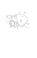
(2)現像装置
図1は実施例1に係る現像装置の断面図である。
(2) Developing Device FIG. 1 is a cross-sectional view of the developing device according to the first embodiment.
本実施例における現像装置40は、開口60と現像スリーブ41とを回転可能に配設した現像室61と、現像剤(以下、トナーT又はトナーという。)を収容した現像剤収容部62(以下、トナー室という)からなる。クリーニングユニットとは別体の現像装置(又は、現像ユニット)として構成させている。
The developing
トナー室の磁性一成分トナーTは、搬送手段であり撹拌手段でもあるトナー攪拌63によって、トナー室62と現像室61の間に連通口であるトナー供給開口60を通じて現像室61へ搬送される。現像室61のトナーTは、現像スリーブ41に内包されたマグネット(図示せず)によって現像ローラ41に引き寄せられる。そして、現像ローラ41のR2方向への回転に伴って弾性部材からなる現像剤規制部材42(現像ブレード)方向に現像剤は搬送され、現像ブレード42によってトリボ付与と層厚規制を受けて感光ドラム20方向に搬送される。
The magnetic one-component toner T in the toner chamber is transported between the
ここで、現像スリーブ41には画像形成装置本体から直流電圧(Vdc=−400V)に交流電圧(ピーク間電圧=1600Vpp、周波数f=2400Hz)を重畳した現像バイアスが印加されている。感光ドラム20は接地されており、現像スリーブ41との対向領域では現像バイアスに応じて電界が発生する。その結果、前述の帯電されたトナーによって感光ドラム20表面の潜像が現像剤像として現像される。
Here, a developing bias in which an AC voltage (peak-to-peak voltage = 1600 Vpp, frequency f = 2400 Hz) is superimposed on a DC voltage (Vdc = −400 V) is applied to the developing
次に、実施例1における現像剤残量検知手段について図1、図4および図7を用いて説明する。図4は実施例1における現像枠体の外側面図である。図7(a)は実施例1におけるサイドホルダの現像枠体と樹脂接合する内側を見た図である。図7(b)は実施例1におけるサイドホルダの現像枠体と樹脂接合しない外側を見た図である。 Next, the developer remaining amount detecting means in the first embodiment will be described with reference to FIGS. FIG. 4 is an outer side view of the developing device frame in the first embodiment. FIG. 7A is a view of the inner side of the side holder in Example 1 where the developing frame and the resin are joined. FIG. 7B is a view of the outside of the side holder in Example 1 where the developing frame and the resin are not joined.
現像剤残量検知手段として、静電容量を検出するための検出部材として、導電性を有するアンテナ部材43を設けている。現像スリーブ41にAC電圧を印加すると、現像スリーブ41とアンテナ部材43との間に、両者間の静電容量に対応した電流が誘起される。同様に、現像スリーブ41と出力用導電経路45との間に関しても、両者間の静電容量に対応した電流が誘起される。ここで、現像スリーブ41とアンテナ部材43との間の静電容量を実質静電容量とし、現像スリーブ41と出力用導電経路45との間の静電容量を浮遊静電容量とする。実質静電容量は、現像スリーブ41とアンテナ部材43間の現像剤量(以下、トナー量という)に応じて変化する。浮遊静電容量は、現像スリーブ41と出力用導電経路45間のトナー量に応じて変化する。この二つの静電容量はそれぞれのトナーの量に応じて変化し、現像剤量検出装置(トナー量検出装置)70には、実質静電容量と浮遊静電容量の合計に対応した電流が1つの信号として伝わる。
As a developer remaining amount detecting means, a
すなわち、アンテナ部材43と出力用導電経路45から流れた検出信号(電流)をサイドホルダ49に設けられた接点電極48を介して、画像形成装置1内のトナー量検出装置70に伝達する。そして、トナー量検出装置70で測定することにより現像装置40内のトナー量を逐次に予測(検出)することが可能となる。
That is, a detection signal (current) flowing from the
本実施形態では、一方の電極に現像スリーブを用いているが、現像スリーブとは別に他の電極を設けてもよい。つまり、検出部材と対向する位置に、静電容量を用いて現像剤量を検出するための電極を別途設けることも可能である。当然、現像スリーブを電極として用いなくてもよい。 In this embodiment, the developing sleeve is used for one electrode, but another electrode may be provided separately from the developing sleeve. That is, it is possible to separately provide an electrode for detecting the developer amount using the electrostatic capacitance at a position facing the detection member. Of course, the developing sleeve may not be used as an electrode.
図1に示すとおり、アンテナ部材43は現像枠体44の底面に設けられる事で、現像装置40内のトナー量の変化を知る事が出来る。図5は実施例1において、アンテナ部材および出力用導電経路が位置公差中心に配置された場合の現像装置内のトナー量と静電容量の関係を表した図である。図5は、横軸に現像剤残量(以下、トナー残量という)、縦軸に各々のトナー残量に応じた静電容量を示している。本実施例では図5に示すように、トナーを消費し、トナー量が80g程度になった時点から、トナーが無くなるまでの静電容量の変化を利用する事でユーザーにトナー残量および交換時期を知らせる事ができる。アンテナ部材43と現像スリーブ41との間のトナー量が変化し始めるのが80gになっているため、80gよりもトナー量が多い領域では静電容量は変化しない。なお、容器の形態に応じ、トナー残量を効率良く計測できる場所であれば、アンテナ部材の取り付け位置は任意に決定できる。
As shown in FIG. 1, the
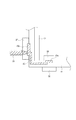
(2−1)検出部材(アンテナ部材)の構成
以下に、アンテナ部材43の構成について説明する。図6は実施例1における現像装置のアンテナ部材の概略を表わした断面図である。図1および図4に示す点線Fにおける断面図になっている。
(2-1) Configuration of Detection Member (Antenna Member) The configuration of the
アンテナ部材43は、現像枠体44の底面の一部に現像スリーブ41に対向するようにSUSの板を両面テープ46で貼り付けることで構成されている。つまり、本実施例においては、SUS板をアンテナ部材として用いる。出力用導電経路45との導通は、出力用導電経路45のある端部において導電性の両面テープ47を介してなされている。アンテナ部材43に関しては、導電性を有する部材であれば自由に選択できる。出力用導電経路45との導通に関しては、導通が取れるならば、導電性の両面テープだけでなく、板バネによる直接接触や、導電性グリスを使ったものであっても構わない。
The
ここで、アンテナ部材および出力用導電経路の意味を説明する。アンテナ部材は、導電性部材であって、トナー量の変化によって変化する静電容量を検出できる場所にあればよい。そのため、本実施例では、アンテナ部材とは現像スリーブに対向する位置、且つ、トナーを収容している現像枠体の内壁面より内側に位置する。また、アンテナ部材は導通のある複数の部材から成っていてもよい。また、後述するが、アンテナ部材は、導電樹脂シートでもよい。例えば、ポリスチレン樹脂(以下、PS樹脂という)にカーボンブラックを分散させ導電性を持たせた導電樹脂シートを用いてもよい。樹脂は、ポリスチレン樹脂に限らず、エチレンビニルアセテート樹脂(以下、EVA樹脂という。)でもよい。また、導電樹脂シートは単層だけでなく複数の層から構成されてもよい。実施例1においては、図6に示すように、枠体44の現像剤を収容する側の側壁面44aより内側にアンテナ部材を配置している。つまり、点線Mよりも内側に位置する。
Here, the meaning of the antenna member and the output conductive path will be described. The antenna member is a conductive member, and may be located where a capacitance that changes with a change in toner amount can be detected. For this reason, in this embodiment, the antenna member is located at a position facing the developing sleeve and inside the inner wall surface of the developing device frame housing the toner. The antenna member may be composed of a plurality of conductive members. As will be described later, the antenna member may be a conductive resin sheet. For example, a conductive resin sheet in which carbon black is dispersed in polystyrene resin (hereinafter referred to as PS resin) to have conductivity may be used. The resin is not limited to polystyrene resin, but may be ethylene vinyl acetate resin (hereinafter referred to as EVA resin). Moreover, the conductive resin sheet may be composed of a plurality of layers as well as a single layer. In the first embodiment, as shown in FIG. 6, the antenna member is disposed on the inner side of the side wall surface 44 a of the
一方、出力用導電経路とは、樹脂を含む導電性部材であって、アンテナ部材によって受けた信号を伝達する。アンテナ部材からの信号を装置の外側に送るために内側壁面より外側の部分にも配置されている。本実施例においては、内側壁面よりも外側に位置する導電経路が樹脂を含んでいることにより、位置精度や部品寸法精度のばらつきを低減することができる。 On the other hand, the output conductive path is a conductive member containing a resin and transmits a signal received by the antenna member. In order to send the signal from the antenna member to the outside of the apparatus, the antenna member is also arranged on the outer side of the inner wall surface. In the present embodiment, since the conductive path located outside the inner wall surface contains resin, it is possible to reduce variations in positional accuracy and component dimensional accuracy.
また、導電経路の一部は、枠体の内部に伸びて設けられ枠体の現像剤を収容する側とその反対側に電気的な接続ができるように配置されている。そのため、用途によっては、枠体の現像剤を収容する側とその反対側の壁面に導電経路の一部が露出した形になる。後述するが、図26や図27に示す導電経路の一部が露出しているものでもよい。枠体も樹脂であるため、枠体と導電経路とを樹脂成形で一体的に形成することができるため、組み立て性が向上する。 In addition, a part of the conductive path is provided so as to extend inside the frame body, and is arranged so that electrical connection can be made between the side of the frame body containing the developer and the opposite side. Therefore, depending on the application, a part of the conductive path is exposed on the side of the frame body on which the developer is accommodated and on the opposite wall surface. As will be described later, a part of the conductive path shown in FIGS. 26 and 27 may be exposed. Since the frame is also resin, the frame and the conductive path can be integrally formed by resin molding, so that the assemblability is improved.
(2−2)接点電極の構成
以下に接点電極の構成について説明する。図7(a)は実施例1におけるサイドホルダの現像枠体と樹脂接合する内側を見た図である。図7(b)は実施例1におけるサイドホルダの現像枠体と樹脂接合しないサイドホルダの外側を見た図である。
(2-2) Structure of contact electrode The structure of a contact electrode is demonstrated below. FIG. 7A is a view of the inner side of the side holder in Example 1 where the developing frame and the resin are joined. FIG. 7B is a view of the outer side of the side holder that is not resin-bonded to the developing frame of the side holder in the first embodiment.
接点電極48は銅電極板をサイドホルダ49の凸ボスに嵌め込むことで固定されている。接点電極48の凸ボス嵌め込み部48aは、接点電極48にコの字状の切れ込みによって作られている。また接点電極48はサイドホルダ穴部49aを通過するように折り曲げられている。サイドホルダ49を現像枠体44に樹脂接合することで、接点電極48の板バネ形状になっている接点電極48の出力用導電経路接触部48bが、図4に示す出力用導電経路45の接点電極接触部45bに接触することで導通する。加えて、接点電極48は画像形成本体1との接触部を有している。そのため、プロセスカートリッジが本体に装着されている際は、アンテナ部材42および出力用導電経路45からの信号を画像形成本体1のトナー量検出装置70に伝えることができる。
The
(2−3)出力用導電経路および現像枠体の構成
次に、本実施例の特徴である出力用導電経路45と現像枠体44について詳細に説明する。
(2-3) Configuration of Output Conductive Path and Development Frame Body Next, the output
〔出力用導電経路の形成方法〕
以下に、出力用導電経路45の形成方法について説明する。図4は実施例1における現像枠体の側面図である。図6は実施例1における現像装置のアンテナ部材の概略を表わした図である。図8は実施例1における出力用導電経路を現像枠体に対して一体成型する際に金型を現像枠体に当接させて型締めした状態の概略断面図である。図9は実施例1における出力用導電経路と現像枠体の概略断面図である。
[Method for forming conductive path for output]
A method for forming the output
出力用導電経路45は、現像枠体44と金型27および金型28との間に形成された空間(出力用導電経路形成部)を利用して作る。出力用導電経路45を形成するための空間に、ゲート33から導電性樹脂が注入することで、出力用導電経路を現像枠体44と一体成型する。ここで、出力用導電経路形成部とは、現像枠体44に金型27と金型28を当接して配置させて形成される現像枠体44と金型(27、28)との間の空間と、樹脂注入される枠体44内部の空間のことである。
The output
出力用導電経路45を形成する際に、金型27と金型28を当接させて型締めする必要があり、バックアップ部材31とバックアップ部材32がそれぞれ金型当接面の裏側から支持している。これは金型の押し付け力や樹脂注入時の樹脂圧によって現像枠体44の当接面が逃げることや、変形することを生じさせないためである。本実施例では、型当接面の裏側を支持しているが、支持する部分は裏側でなくても現像枠体44の逃げや変形を抑えることができる部分であれば構わない。
When the output
図9に示すように、金型28で成型された導電経路の一部であるアンテナ部材接触部45aが、アンテナ部材43に対して、導電性両面テープ47を介して接触することでアンテナ部材43との導通をとる。そして、金型27で成型された接点電極接触部45bが、接点電極48の出力用導電経路接触部48bと接触することで、接点電極48と導通する。本実施例においては、成型後の枠体に樹脂を注入する一体成型の方法を用いたが、枠体の成型時に同一型内で行うインサート成型や二色成型の方法を用いることもできる。
As shown in FIG. 9, the antenna
現像枠体44は材料として耐衝撃性ポリスチレン(以下、HIPSという。)を用いている。出力用導電経路45は、カーボン分散PS樹脂、導電性のHIPS樹脂等の樹脂を用い、現像枠体44のHIPSに対して相溶性を有するものであれば良い。また、相溶性を有する事がなくても、例えば、カーボン分散EVAのように表面に接着性を有する材料であっても良い。
The developing
次に、比較例を説明する。 Next, a comparative example will be described.
〔比較例〕
図10は比較例における出力用導電経路を両面テープによって貼り付けた構成の概略図を表わしている。比較例は、成型後の現像枠体44にSUSの出力用導電経路45を両面テープ46によって固定した。アンテナ部材42および接点電極48は本実施例と同様の構成を用い、導通方法も同様の構成を用いた。
[Comparative example]
FIG. 10 is a schematic diagram of a configuration in which the output conductive path in the comparative example is attached with a double-sided tape. In the comparative example, the SUS output
ここで、出力用導電経路45について本実施例と比較例の位置公差を比較する。本実施例は、現像スリーブ41の位置決めをしている現像枠体44に対して、導電経路の樹脂が一体成型されている。また、出力用導電経路45とアンテナ部材43の接触部における公差、出力用導電経路45と接触電極48の接触部における公差がある。そのため、枠体の成型公差と、樹脂の成型公差、出力用導電経路45とアンテナ部材43の接触部における公差、出力用導電経路45と接触電極48の接触部における公差の4つの積み上げ公差が本実施例の位置公差となる。比較例は、現像スリーブ41の位置決めをしている現像枠体44に対して、SUSの出力用導電経路45が両面テープ34で貼り付けられている。そのため、枠体の成型公差と、SUSの出力用導電経路45の厚み公差と曲げ位置の寸法公差、両面テープ34の厚み公差、現像枠体44への貼り付け公差の5つがある。さらに、出力用導電経路45とアンテナ部材43の接触部における公差、出力用導電経路45と接触電極48の接触部における公差の7つの積み上げ公差が位置公差となる。金型を用いて樹脂を成型する際には、射出成型時の条件を一定にすることで比較的容易に位置精度よく成型することができる。それに対して、貼り付けは自動機による貼り付けでも、人の手による貼り付けでも、ある程度の大きさの公差が生まれてしまう。比較例は、実施例1に対して、貼り付け公差に加えて、導電経路の厚み公差と曲げ公差と両面テープの厚み公差がある。複数の公差の積み上げを無くし、導電経路の樹脂を枠体と一体成型によって出力用導電経路45を作ることで、従来の金属の導電経路を貼り付けた場合に対して、位置精度が明らかに向上する。つまり、導電経路に樹脂を含むことにより加工が容易であるため、SUSを導電経路に用いた場合の厚み公差や曲げ位置の寸法公差などを低減することが可能になる。これにより本実施例では、公差の発生する箇所を少なくすることができ、位置精度が向上できる。それと同時に、組み立て性や構造の簡素化を図ることができる。
Here, the positional tolerances of the present embodiment and the comparative example are compared for the output
次に本実施例と比較例の位置公差とトナー残量の検知精度について説明する。ここでは、本実施例と比較例のそれぞれにおいて、製造で出来得る現像スリーブ41と出力用導電経路45の位置が一番遠くなるものと一番近くなるものを用いて説明する。
Next, the detection accuracy of the position tolerance and the remaining amount of toner in this embodiment and the comparative example will be described. Here, in each of the present embodiment and the comparative example, description will be made using the developing
出力用導電経路45が検出する浮遊静電容量は、現像スリーブ41と出力用導電経路45間の静電容量のため、距離が大きく静電容量に関係する。そのため、公差内における現像スリーブ41と出力用導電経路45の位置が一番遠くなる位置と一番近くなる位置の静電容量を実際のトナー量と比較することで、トナー残量検知精度を比較することができる。図11は実施例1における現像スリーブとアンテナ部材と出力用導電経路の位置を示した図である。アンテナ部材の長手方向に交差するように出力用導電経路の一部(第1の導電経路)が形成されている。多くの場合は、現像装置のアンテナ部材の長手方向と直交する方向に導電経路の一部(第1の導電経路)が配置されることになる。図11(a)に示す領域Pが現像スリーブ41とアンテナ部材43がトナーを検知できる範囲となる。図11(b)に示す領域Qが現像スリーブ41と出力用導電経路45がトナーを検知できる範囲である。領域Qは領域Pに対してトナー量が少ない時に、静電容量の増減が起きる。そのため、浮遊静電容量の振れはトナー量が少ない時に影響が大きい。また現像スリーブ41と出力用導電経路45の距離が近いほど静電容量も大きくなるため、領域Qの中で両者の距離が近い範囲のトナー量が静電容量の大部分を占める。比較例も同様の構成になっている。
The stray capacitance detected by the output
図12は実施例1における静電容量とトナー量のグラフである。図13は比較例における静電容量とトナー量のグラフである。図14は6〜8pFの領域における静電容量とトナー量のグラフである。本実施例において、現像スリーブ41と出力用導電経路45の位置が一番近くなるものを(A)、現像スリーブ41と出力用導電経路45の位置が一番遠くなるものを(B)とする。比較例において、現像スリーブ41と出力用導電経路45の位置が一番近くなるものを(C)、現像スリーブ41と出力用導電経路45の位置が一番遠くなるものを(D)とする。ただし、アンテナ部材42に関しては、全て位置公差の中心位置に取り付けられている。
FIG. 12 is a graph of electrostatic capacity and toner amount in Example 1. FIG. 13 is a graph of capacitance and toner amount in the comparative example. FIG. 14 is a graph of capacitance and toner amount in the region of 6-8 pF. In the present embodiment, the developing
それぞれ、現像スリーブ41と出力用導電経路45の位置が一番近くなる位置(A)と(C)が、静電容量として大きくなり、現像スリーブ41と出力用導電経路45の位置が一番遠くなる位置(B)と(D)が、静電容量として小さくなっている。これは浮遊静電容量の大小によって、測定される静電容量に大小が生まれているからである。例えば、図14に示した通り、静電容量が7pFで比較すると、実施例1では23〜32g、比較例では16〜37gのばらつきが発生する。つまり、実施例1は比較例に対して、トナー残量検知の精度が向上していることがわかる。そのため、実施例1は、比較例に対して、ユーザーに精度よく交換タイミングを伝えることができる。
The positions (A) and (C) at which the positions of the developing
つまり、比較例では、樹脂を用いて導電経路を作っていないため、SUSを導電経路に用いた場合の厚み公差や曲げ位置の寸法公差、さらに両面テープ34の厚み公差が発生することになる。これに対して本実施形態では、導電経路が樹脂を含んで構成されることにより、公差の発生する箇所を少なくすることができ、位置精度が向上できる。
That is, in the comparative example, since the conductive path is not made using resin, a thickness tolerance and a dimensional tolerance of the bending position when SUS is used for the conductive path, and a thickness tolerance of the double-
(実施例2)
図15は実施例2における出力用導電経路とアンテナ部材を現像枠体に対して一体成型する際に金型を現像枠体に当接させて型締めした状態の概略断面図である。
(Example 2)
FIG. 15 is a schematic cross-sectional view of a state in which the mold is brought into contact with the developing device frame and clamped when the output conductive path and the antenna member are integrally formed with the developing device frame in the second embodiment.
本実施例は、図15に示す通り実施例1と比べてアンテナ部材43と出力用導電経路45が一体で枠体に成型されていることを特徴としている。その他に関しては、実施例1と同様のため、重複している箇所については説明を省略する。
As shown in FIG. 15, the present embodiment is characterized in that the
〔出力用導電経路とアンテナ部材の一体形成方法〕
出力用導電経路とアンテナ部材を一体に形成する方法ついて説明する。以下、出力用導電経路(75b、75c)とアンテナ部材75aを一体に成型した部材を一体電極75とする。本実施例では、導電経路の一部が内側壁面よりも内側にも伸び、アンテナ部材に接続している部分75dがある。図15は実施例2における出力用導電経路とアンテナ部材を現像枠体に対して一体成型する際に金型を現像枠体に当接させて型締めした状態の概略断面図である。図16は実施例2における現像装置の一体電極の概略を表わした図である。
[Method of integrally forming output conductive path and antenna member]
A method of integrally forming the output conductive path and the antenna member will be described. Hereinafter, a member obtained by integrally molding the output conductive path (75b, 75c) and the
一体電極75は、現像枠体44と金型27および金型28との間に形成された空間に形成する。一体電極75を形成するための空間である一体電極形成部に、ゲート33から導電樹脂が注入されることで、一体電極が現像枠体44と一体成型される。ここで、一体電極形成部とは、現像枠体44に金型27と金型28を当接して配置させた現像枠体44と金型27および金型28との間と、樹脂注入される現像枠体44内部の空間のことである。本実施例においては、ゲート点数が1点となっているが、3点や4点など複数のゲートを用いて一体成型を行っても構わない。一体電極75を形成する際に、金型27と金型28を当接させて型締めする必要があり、バックアップ部材31とバックアップ部材32がそれぞれ金型当接面の裏側から支持している。
The
出力用導電経路とアンテナ部材が一体に成型されることによって、別体で構成されていた際に発生していた接触部における位置公差の振れが無くなる。加えて、一体に成型できることで、より確実な導通の確保や、部品点数および製造に必要な工数を削減することができる。そのため、安価で精度のよい残量検知構成を提供できる。本実施例においては、成型後の枠体に樹脂を注入することで一体成型する方法を用いたが、枠体の成型時に同一型内でインサート成型や二色成型を行う方法を用いることもできる。 By forming the output conductive path and the antenna member integrally, the positional tolerance fluctuation at the contact portion that has occurred when the output conductive path and the antenna member are formed separately is eliminated. In addition, since it can be integrally molded, more reliable conduction can be ensured, and the number of parts and man-hours required for manufacturing can be reduced. Therefore, an inexpensive and accurate remaining amount detection configuration can be provided. In the present embodiment, a method of integrally molding by injecting resin into the molded frame body is used, but a method of performing insert molding or two-color molding in the same mold at the time of molding the frame body can also be used. .
また、実施例2の変形例として、出力用導電経路とアンテナ部材と接点電極の三体を一体に成型する構成もある。 In addition, as a modification of the second embodiment, there is a configuration in which the output conductive path, the antenna member, and the contact electrode are integrally molded.
(変形例)
図17は実施例2における出力用導電経路とアンテナ部材と接点電極を現像枠体に対して一体成型する際に金型を現像枠体に当接させて型締めした状態の概略断面図である。図18(a)は変形例におけるサイドホルダの現像枠体と樹脂接合する内側を見た図である。図18(b)は変形例におけるサイドホルダの現像枠体と樹脂接合しない外側を見た図である。
(Modification)
FIG. 17 is a schematic cross-sectional view of a state in which the mold is brought into contact with the developing frame and clamped when the output conductive path, the antenna member, and the contact electrode are integrally formed with the developing frame in the second embodiment. . FIG. 18A is a view of the inner side of the side holder in the modified example where the developing frame and the resin are joined. FIG. 18B is a view of the outside of the side holder in the modified example where the developing frame and the resin are not joined.
変形例では、一体電極75が出力用導電経路とアンテナ部材と接点電極の三体を一体に成型した部材になっている。一体電極75は、現像枠体44と金型27および金型28との間に形成された空間に形成される。そして、一体電極75を形成するための空間である一体電極形成部に、ゲート33から導電樹脂が注入されることで、一体電極と現像枠体44とが一体成型される。ここで、一体電極形成部とは、現像枠体44に金型27と金型28を当接して配置させた現像枠体44と金型27および金型28との間と、樹脂注入される現像枠体44内部の空間のことである。一体電極75を形成する際に、金型27と金型28を当接させて型締めする必要があり、バックアップ部材31とバックアップ部材32がそれぞれ金型当接面の裏側から支持している。
In the modification, the
サイドホルダ49は、一体電極75がサイドホルダから露出するための穴49cを有している。そのため、一体電極75の一部が、穴49cから露出しており、画像形成装置本体の接点部と接触可能になっている。
The
出力用導電経路とアンテナ部材と接点電極の三体を一体に成型することで、実施例2よりも、接点電極に関する部品点数および構造が簡素化することにより製造に必要な工数を削減することができる。本実施例においては、成型後の枠体に樹脂を注入することで一体成型する方法を用いたが出力用導電経路とアンテナ部材をインサート成型によって形成した後に、接点電極を枠体に樹脂を注入することで一体成型する構成も可能である。 By integrally molding the output conductive path, the antenna member, and the contact electrode, the number of parts and the structure related to the contact electrode can be simplified and the number of steps required for manufacturing can be reduced compared to the second embodiment. it can. In this embodiment, a method of integrally molding by injecting resin into the molded frame was used, but after forming the output conductive path and the antenna member by insert molding, the contact electrode was injected into the frame. By doing so, it is also possible to adopt a structure in which the molding is performed integrally.
(実施例3)
図19は実施例3における出力用導電経路と現像枠体の概略断面図である。本実施例は、実施例1と比べて、現像枠体44に一体成型されている出力用導電経路45について、現像枠体44および現像スリーブ41に対する位置決め方向に特徴がある。その他に関しては、実施例1と同様のため、重複している箇所については説明を割愛する。
(Example 3)
FIG. 19 is a schematic cross-sectional view of the output conductive path and the developing device frame in the third embodiment. The present embodiment is characterized in the positioning direction with respect to the developing
本実施例の出力用導電経路45は、実施例1と同様に、現像枠体44と金型の間に導電樹脂が注入することで成型される。この導電樹脂を注入する際の樹脂の温度は、樹脂が溶融する温度以上であり、170℃の溶融した樹脂を注入している。そのため、出力用導電経路45を成型した際に、注入した樹脂が常温に冷めるまでの間、樹脂の収縮が起こる。また、浮遊静電容量は、出力用導電経路45の現像スリーブ41側の表面から現像スリーブ41までの距離によって決まる。したがって、樹脂を含む出力用導電経路45の現像スリーブ41側の表面を、現像枠体44に対して接触するように固定することで浮遊静電容量の振れを低減することができる。以下、樹脂と樹脂が接触した状態で固定していることを、接触固定しているとする。本実施例では、樹脂を含む出力用導電経路45の現像スリーブ41側の表面と現像枠体44を接触固定するためのアンカー形状78を有している。このアンカー形状78は、樹脂の幅が大きいほど樹脂が大きく収縮することを利用している。出力用導電経路45の長手Kと長手Lが、短手Mと短手Nに対して大きく収縮する。上記の特性により、出力用導電経路45が長手KおよびLの方向に収縮し、アンカー形状78によって、現像枠体44の現像スリーブ41側に出力用導電経路45が押しつけられる。結果、出力用導電経路45の現像スリーブ41側が現像枠体44に接触固定される。
As in the first embodiment, the output
ここで、出力用導電経路45の現像スリーブ41側の表面について、図20を用いて説明する。図20は、出力用導電経路45の現像スリーブ41側の表面を説明するためのモデル図である。出力用導電経路45の現像スリーブ41側の表面とは、出力用電極45の表面上の任意の点であって、現像スリーブ41の中心とその任意の点とを結んだ線分上に、出力用導電経路45の表面がない点の集合からなる面のことを指す。図20で、現像スリーブ41の中心である点Gから、出力用導電経路45の表面上の点Hまでの線分上に、出力用導電経路45の表面がないことがわかる。そのため、点Hは出力用導電経路45の現像スリーブ41側の表面上の点となる。対して、現像スリーブ41の中心である点Gから、出力用導電経路45の表面上の点Iまでの線分上には、出力用導電経路45の表面上の点Jが存在する。したがって、点Iは出力用導電経路45の現像スリーブ41側の表面上の点とはならない。点Hの様にその点から現像スリーブ41の中心までの線分上に出力用導電経路45の表面がない点の集合によって、出力用導電経路45の現像スリーブ41側の表面は形成されている。
Here, the surface of the output
もちろん、出力用導電経路45の現像スリーブ41側の表面を、現像枠体44に対して接触固定する方法であれば、実施例3のアンカー形状78で無くても構わない。例えば、接触固定したい現像枠体の表面に細かい凹凸を設けることでアンカー効果を利用する方法や、現像枠体と成型される出力用導電経路の間に接着性の物質が介在する構成等である。また、注入した樹脂を冷却する過程において冷却スピードに差をつけることで、意図的に出力用導電経路に反りを発生させて現像枠体に押し当てる形状にしてもよい。
Needless to say, the
(実施例4)
図21は実施例4における出力用導電経路と現像枠体の概略断面図である。図22は実施例2における出力用導電経路と現像枠体の概略断面図である。本実施例は、実施例2と比べて、現像枠体44に一体成型されている一体電極75について、接点電極48と接触しない側の端部に特徴がある。その他に関しては、実施例2と同様のため、重複している箇所については説明を省略する。
Example 4
FIG. 21 is a schematic cross-sectional view of the output conductive path and the developing device frame in the fourth embodiment. FIG. 22 is a schematic sectional view of the output conductive path and the developing device frame in the second embodiment. Compared with the second embodiment, the present embodiment is characterized in that the
本実施例の一体電極75は、図21および図22に示す通り、接点電極48(第1の導電経路)と接触しない側のアンテナ部材の長手方向の端部に、接触電極48と接触する側の端部と同様の形状である補正電極(第2の導電経路)79を設けている。接点電極48と補正電極79は、アンテナ部材の長手方向において、交差する方向に伸びており、かつアンテナ部材を挟んだ位置に設けられている。
As shown in FIGS. 21 and 22, the
補正電極(第2の導電経路)79は、一体電極75の一部であり、実施例1と同様に、現像枠体44と金型の間に導電樹脂が注入することで成型される。補正電極79を設けることで、トナーの現像室61内の長手の偏りに対して変動する浮遊静電容量の振れを低減することができる。その詳細を以下に説明する。
The correction electrode (second conductive path) 79 is a part of the
図22は実施例2におけるトナーの偏った際の現像スリーブと一体電極の位置を示した図である。図22(a)は接点電極側にトナーが偏った図、(b)はその逆側にトナーが偏った図である。図23は実施例4におけるトナーの偏った際の現像スリーブと一体電極の位置のモデル図である。図23(a)は接点電極側にトナーが偏った図であり、図23(b)はその逆側にトナーが偏った図である。斜線の領域Yは実施例2における浮遊静電容量として検知する領域、斜線の領域Zは実施例4における浮遊静電容量として検知する領域である。点線の領域Xはトナーの偏っている様子を表わしている。図22および図23の(a)と(b)のトナー量は同量になっている。そのため、検知する浮遊静電容量はそれぞれ同じであることが望ましい。領域Yと領域Zでは、領域Zのほうがトナーの偏りに対して広い範囲をカバーできている。したがって、実施例4は実施例2よりも、同量のトナーが偏った様々な場合に対して、検出される浮遊静電容量のばらつきを少なくすることができる。もちろん、補正電極は、出力用導電経路(一体電極の一部分)が検知する浮遊静電容量の同一トナー量に対するばらつきを抑える形状であればこの形状に限らない。補正電極79を一体電極の一部として現像枠体44に一体成型することで、部品点数や工数も増えることなく形成できている。
FIG. 22 is a diagram illustrating the positions of the developing sleeve and the integral electrode when the toner is biased in the second embodiment. FIG. 22A is a diagram in which the toner is biased toward the contact electrode side, and FIG. 22B is a diagram in which the toner is biased toward the opposite side. FIG. 23 is a model diagram of positions of the developing sleeve and the integral electrode when the toner is biased in the fourth embodiment. FIG. 23A is a diagram in which the toner is biased toward the contact electrode side, and FIG. 23B is a diagram in which the toner is biased toward the opposite side. A hatched region Y is a region detected as a floating capacitance in the second embodiment, and a hatched region Z is a region detected as a floating capacitance in the fourth embodiment. A dotted area X represents a state where toner is biased. The toner amounts in FIGS. 22 and 23 are the same. Therefore, it is desirable that the floating capacitances to be detected are the same. In the area Y and the area Z, the area Z can cover a wider range with respect to the deviation of the toner. Therefore, the variation in the detected floating electrostatic capacity can be reduced in the fourth embodiment compared to the second embodiment in various cases where the same amount of toner is biased. Of course, the correction electrode is not limited to this shape as long as it has a shape that suppresses variations in floating electrostatic capacitance detected by the output conductive path (a part of the integral electrode) with respect to the same toner amount. The
〔その他〕
これまでの説明では、検出部材の長手方向に交差する枠体の内側壁面は直交する位置関係にあるものであったが、図24に示すように傾斜していてよい。その場合は、傾斜面を延長する仮想面を作り、その仮想面を境に外側に配置されているものが樹脂を含む導電経路75cであればよい。図24に示されるように、アンテナ部材と導通するためには、アンテナ部材の方に伸びる導電経路75dも必要になり、導電経路の端部と導電性の両面テープとを介してアンテナ部材に接続している。
[Others]
In the description so far, the inner wall surface of the frame that intersects the longitudinal direction of the detection member has an orthogonal positional relationship, but may be inclined as shown in FIG. In that case, a virtual surface that extends the inclined surface is formed, and the
また、一体成型において、導電経路と検出部材と接触部や接点電極を一体的に成型することを説明したが、一体成型の組み合わせは、製造するものによって適宜選択すればよい。例えば、枠体が、検出部材、導電経路、接触部の少なくとも1つを用途に応じて一体成型すればよい。 Further, in the integral molding, it has been described that the conductive path, the detection member, the contact portion and the contact electrode are integrally molded. However, the combination of the integral molding may be appropriately selected depending on what is manufactured. For example, the frame may be formed integrally with at least one of the detection member, the conductive path, and the contact portion depending on the application.
その他の例としては、枠体が、検出部材、導電経路、接点電極の少なくとも1つと一体成型することも考えられる。 As another example, it is conceivable that the frame is integrally formed with at least one of the detection member, the conductive path, and the contact electrode.
また、本実施例の説明では、現像装置の導電経路が樹脂を含む構成について説明した。しかし、現像剤担持体がなく現像剤を収容する現像剤容器にも現像剤量を検出する機構を設ける場合はあり、その場合には、現像剤容器にも応用は可能である。本実施例の現像装置の一部を現像剤容器として考えてもよい。 In the description of this embodiment, the configuration in which the conductive path of the developing device includes a resin has been described. However, there is a case where a mechanism for detecting the amount of developer is also provided in a developer container that does not have a developer carrier and accommodates the developer, and in that case, the present invention can also be applied to the developer container. A part of the developing device of this embodiment may be considered as a developer container.
(実施例5)
次に本発明に係る実施例5について図25から図27を用いて説明する。図25(a)は実施例5における出力導電経路45の配置例を示す概略斜視図であり、図25(b)はその断面図である。図26(a)は実施例5における出力導電経路45の他の配置例を示す概略斜視図であり、図26(b)はその断面図である。図27(a)は実施例5における出力導電経路45の他の配置例を示す概略斜視図であり、図27(b)はその断面図である。
(Example 5)
Next, a fifth embodiment according to the present invention will be described with reference to FIGS. FIG. 25A is a schematic perspective view showing an arrangement example of the output
本実施例は、実施例1とは異なる出力用導電経路とアンテナ部材の配置例について説明するものである。その他の基本構成については実施例1と同様のため、重複している箇所については説明を省略する。 In this embodiment, an output conductive path and an antenna member, which are different from the first embodiment, will be described. Since the other basic configuration is the same as that of the first embodiment, the description of the overlapping portions is omitted.
本実施例において、出力用導電経路45は図25(b)に示すように、現像枠体44内側の底面の一部に設けられたアンテナ部材43と導通するように現像枠体44上に導電樹脂で一体成形されている。この時、アンテナ部材43と出力用導電経路45間の導通方法は導通性が確保できれば良いため、直接接触でも導電性の両面テープ等を介してでも構わない。しかし、両面テープ等では公差等が発生するため直接接触させる構成が好ましい。そして、出力用導電経路45は現像枠体44の内部を通り、その一部が現像枠体44の外側に露出するように形成されており、露出部の一部には外部に設けられた接点と接触して電気的な接続をするための接点電極接触部45bが設けられている。
In this embodiment, as shown in FIG. 25B, the output
本実施例では、アンテナ部材43と対向する位置に、静電容量を用いて現像剤量を検出するための電極31を設けており、アンテナ部材43と電極31との間の静電容量を測定している。
In this embodiment, the
本実施例における出力用導電経路45の配置例として、図25(a)(b)に示すように、アンテナ部材43の厚み方向から見て、出力用導電経路45全体がアンテナ部材43設置領域内(設置範囲内)に重なるように配置するケースが挙げられる。この場合、電極31から見て出力用導電経路45はアンテナ部材43の後ろに隠れているため、実施例1で挙げたような電極31(実施例1では現像スリーブ41)と出力用導電経路45間で発生する浮遊静電容量は発生しない。
As an example of the arrangement of the output
次に、本実施例における出力用導電経路45のその他の配置例を説明する。その他の配置例として、図26(a)(b)に示すように、アンテナ部材43の厚さ方向から見て、出力用導電経路45の一部をアンテナ部材43設置領域内(設置範囲内)からはみ出して配置するケースが挙げられる。この場合、アンテナ部材43と電極31との間の静電容量の他、電極31と出力用導電経路45の間で浮遊静電容量が発生する。
Next, another arrangement example of the output
次に、本実施例におけるアンテナ部材43の配置例について説明する。実施例1では、アンテナ部材43を現像枠体44の現像剤収納側に設けていたが、アンテナ部材43は図27に示すように、現像枠体44の外側に設けてもよい。この場合も、アンテナ部材43と電極31との間の静電容量の他、電極31と出力用導電経路45の間で浮遊静電容量が発生する。
Next, the example of arrangement | positioning of the
また、本実施例のように出力用導電経路45を現像枠体44上に導電樹脂で一体成形する場合、現像枠体44の材料に対して出力導電経路45の材料は相溶性を有するものを選択することで材料間の結合力を確保することができる。相溶性を有さない材料の組み合わせの場合は、例えば、図26に示すように直線経路や曲線経路、角や円形状等を組み合わせや、厚み違いなどの組み合わせで導電経路を形成する。これにより、導電樹脂一体成形時の熱収縮で現像枠体44に食いつくような形状とすることで、材料間の結合力を補う方法がある。その他の方法としては、出力用導電経路45の材料に熱接着性を有する材料を採用する方法もある。
Further, when the output
以上説明したように、本実施例によれば、本実施例によれば、構造の簡素化が可能になる。さらに、導電経路及び外部接続接点部に板金を用いる場合に比べ、組み付け工程を簡素化し、位置精度や組み付け精度を向上させることができる。 As described above, according to the present embodiment, the structure can be simplified according to the present embodiment. Furthermore, as compared with the case where sheet metal is used for the conductive path and the external connection contact portion, the assembling process can be simplified and the positional accuracy and the assembling accuracy can be improved.
〔その他〕
本発明は、現像剤を収容する現像剤容器だけでなく、現像剤を担持する現像剤担持体(例えば、現像ローラ)を有する現像装置でも利用することができる。もちろん、図2に示すような像担持体を有するプロセスカートリッジ内に現像剤を収容し、一対の電極を配置する構成でもよい。
[Others]
The present invention can be used not only in a developer container containing a developer but also in a developing device having a developer carrying member (for example, a developing roller) carrying a developer. Of course, the developer may be accommodated in a process cartridge having an image carrier as shown in FIG. 2 and a pair of electrodes may be arranged.
また、実施例1では、1つのプロセスカートリッジが着脱可能な構成について説明したが、これに限定されるものではなく、複数のプロセスカートリッジを着脱可能な画像形成装置などでも応用できる。もちろん、複数の現像剤容器や複数の現像装置を着脱可能な画像形成装置でもよい。 In the first embodiment, the configuration in which one process cartridge can be attached / detached has been described. However, the present invention is not limited to this, and can be applied to an image forming apparatus in which a plurality of process cartridges can be attached / detached. Of course, an image forming apparatus in which a plurality of developer containers and a plurality of developing devices can be attached and detached may be used.
40 現像装置
41 現像剤担持体(現像スリーブ)
43 検出部材(アンテナ部材)
44 現像枠体
45 出力用導電経路
45a アンテナ部材接触部
45b 接点電極接触部
47 導電性両面テープ
48 接点電極
40 Developing
43 Detection member (antenna member)
44 Developing
Claims (14)
現像剤を収容する枠体と、
長手方向を有する形状をした電極と、
前記長手方向に延び、前記枠体の前記現像剤を収容する内側に設けられ、前記電極との間にある前記現像剤の量に応じた電流の信号を出力する検出部材と、
前記検出部材と繋がっており、且つ前記長手方向と交差する前記枠体の面で前記枠体の外側に露出する露出部を有し、前記露出部により前記検出部材に流れる電流の信号を前記枠体の外部に出力する、導電性樹脂で構成される導電樹脂部材と、を有し、前記枠体と前記導電樹脂部材とは一体成形されていることを特徴とする現像剤容器。 A developer container for containing the developer,
A frame housing the developer;
An electrode having a shape having a longitudinal direction;
A detection member that extends in the longitudinal direction and that is provided inside the frame body for containing the developer, and that outputs a signal of a current corresponding to the amount of the developer between the electrodes,
It has an exposed portion that is connected to the detection member and is exposed to the outside of the frame at the surface of the frame that intersects the longitudinal direction, and a signal of a current flowing through the detection member by the exposed portion is transmitted to the frame. And a conductive resin member made of a conductive resin that outputs to the outside of the body, wherein the frame and the conductive resin member are integrally molded.
前記サイドホルダには穴が形成されており、前記露出部は、前記穴より露出し、前記現像剤容器が装着される画像形成装置本体の接点部と電気的に接触可能であることを特徴とする請求項1に記載の現像剤容器。 Having a side holder on the outside of the frame,
A hole is formed in the side holder, and the exposed portion is exposed from the hole and can be electrically contacted with a contact portion of an image forming apparatus main body to which the developer container is mounted. The developer container according to claim 1.
前記第1の導電樹脂部材と前記第2の導電樹脂部材は、前記検出部材を挟む位置に設けられていることを特徴とする請求項1から5のいずれか1項に記載の現像剤容器。 A part of the conductive resin member includes a first conductive resin member and a second conductive resin member as the exposed portion,
6. The developer container according to claim 1, wherein the first conductive resin member and the second conductive resin member are provided at positions sandwiching the detection member. 6.
現像剤を担持する現像剤担持体と、を有することを特徴とする現像装置。 A developer container according to any one of claims 1 to 11,
And a developer carrying member for carrying the developer.
現像剤像を担持する像担持体と、を有することを特徴とするプロセスカートリッジ。 A developing device according to claim 12,
A process cartridge having an image carrier for carrying a developer image.
記録材に現像剤像を転写する転写手段と、を有することを特徴とする画像形成装置。 Any one of the developing device according to claim 12 and the process cartridge according to claim 13;
An image forming apparatus comprising: a transfer unit that transfers a developer image to a recording material.
Priority Applications (2)
| Application Number | Priority Date | Filing Date | Title |
|---|---|---|---|
| JP2014152906A JP6468747B2 (en) | 2013-09-24 | 2014-07-28 | Developer container, developing device, process cartridge, and image forming apparatus |
| US14/493,586 US9658566B2 (en) | 2013-09-24 | 2014-09-23 | Developer container, developing device, process cartridge, and image forming apparatus |
Applications Claiming Priority (3)
| Application Number | Priority Date | Filing Date | Title |
|---|---|---|---|
| JP2013197215 | 2013-09-24 | ||
| JP2013197215 | 2013-09-24 | ||
| JP2014152906A JP6468747B2 (en) | 2013-09-24 | 2014-07-28 | Developer container, developing device, process cartridge, and image forming apparatus |
Publications (3)
| Publication Number | Publication Date |
|---|---|
| JP2015087747A JP2015087747A (en) | 2015-05-07 |
| JP2015087747A5 JP2015087747A5 (en) | 2017-08-31 |
| JP6468747B2 true JP6468747B2 (en) | 2019-02-13 |
Family
ID=52691051
Family Applications (1)
| Application Number | Title | Priority Date | Filing Date |
|---|---|---|---|
| JP2014152906A Active JP6468747B2 (en) | 2013-09-24 | 2014-07-28 | Developer container, developing device, process cartridge, and image forming apparatus |
Country Status (2)
| Country | Link |
|---|---|
| US (1) | US9658566B2 (en) |
| JP (1) | JP6468747B2 (en) |
Families Citing this family (3)
| Publication number | Priority date | Publication date | Assignee | Title |
|---|---|---|---|---|
| JP6779752B2 (en) * | 2016-11-09 | 2020-11-04 | キヤノン株式会社 | Developer container, developer, process cartridge, image forming device, manufacturing method and mold |
| JP7210152B2 (en) * | 2018-04-03 | 2023-01-23 | キヤノン株式会社 | Developer container, developing device, process cartridge, image forming apparatus, and developer container manufacturing method |
| US10649367B2 (en) * | 2018-07-30 | 2020-05-12 | Ricoh Company, Ltd. | Powder supply device and image forming apparatus incorporating same |
Family Cites Families (14)
| Publication number | Priority date | Publication date | Assignee | Title |
|---|---|---|---|---|
| EP1016939B1 (en) * | 1998-12-28 | 2006-02-01 | Canon Kabushiki Kaisha | Image developing apparatus, process cartridge, electrophotographic image forming apparatus, and development unit frame |
| JP3897504B2 (en) * | 1998-12-28 | 2007-03-28 | キヤノン株式会社 | Developing device, process cartridge, and electrophotographic image forming apparatus |
| JP2001117346A (en) | 1999-10-20 | 2001-04-27 | Canon Inc | Image forming device and developer quantity detecting device |
| JP3658289B2 (en) * | 2000-07-28 | 2005-06-08 | キヤノン株式会社 | Process cartridge and electrophotographic image forming system |
| US6785479B2 (en) * | 2001-12-28 | 2004-08-31 | Canon Kabushiki Kaisha | Image forming apparatus having a control section for detecting an amount of developer and an amount detection method of developer of image forming apparatus |
| JP3862580B2 (en) | 2002-02-27 | 2006-12-27 | キヤノン株式会社 | Developing device and process cartridge |
| US7555231B2 (en) * | 2006-09-14 | 2009-06-30 | Lexmark International, Inc. | Capacitive toner level sensor and methods of use |
| JP4846062B1 (en) * | 2010-08-20 | 2011-12-28 | キヤノン株式会社 | Cartridge and image forming apparatus |
| JP2012168241A (en) * | 2011-02-10 | 2012-09-06 | Canon Inc | Developing unit, process cartridge and image forming device |
| EP2776892B1 (en) * | 2011-11-09 | 2019-06-05 | Canon Kabushiki Kaisha | Cartridge comprising an electrode |
| JP5460824B2 (en) * | 2011-12-09 | 2014-04-02 | キヤノン株式会社 | cartridge |
| JP6000543B2 (en) * | 2011-12-19 | 2016-09-28 | キヤノン株式会社 | Cartridge and cartridge manufacturing method |
| JP6207137B2 (en) * | 2012-09-05 | 2017-10-04 | キヤノン株式会社 | Cartridge and image forming apparatus |
| JP5868456B2 (en) * | 2013-07-12 | 2016-02-24 | キヤノン株式会社 | Developer container, developing device, process cartridge, and image forming apparatus |
-
2014
- 2014-07-28 JP JP2014152906A patent/JP6468747B2/en active Active
- 2014-09-23 US US14/493,586 patent/US9658566B2/en active Active
Also Published As
| Publication number | Publication date |
|---|---|
| US20150086227A1 (en) | 2015-03-26 |
| US9658566B2 (en) | 2017-05-23 |
| JP2015087747A (en) | 2015-05-07 |
Similar Documents
| Publication | Publication Date | Title |
|---|---|---|
| JP3658289B2 (en) | Process cartridge and electrophotographic image forming system | |
| US7630655B2 (en) | Image forming apparatus and developer remaining amount detecting method | |
| US7532828B2 (en) | Image forming apparatus and developer remaining amount detecting method | |
| KR20150008003A (en) | Method of manufacturing developer container, developer container, developing apparatus, process cartridge, and image forming apparatus | |
| US10606210B2 (en) | Development device, process cartridge, and image forming apparatus | |
| JP3848191B2 (en) | Developing device, process cartridge, and electrophotographic image forming apparatus | |
| US10067443B2 (en) | Developer container, developing device, process cartridge, and image forming apparatus incorporating a developer quantity detection unit | |
| US8977162B2 (en) | Developing device and image forming apparatus including the same | |
| JP6468747B2 (en) | Developer container, developing device, process cartridge, and image forming apparatus | |
| US20120121275A1 (en) | Developer remainder amount detection system and image forming apparatus | |
| CN104142615A (en) | Toner cartridge and image forming apparatus | |
| JP6376846B2 (en) | Manufacturing method of developing device frame | |
| JP2012168241A (en) | Developing unit, process cartridge and image forming device | |
| JP2018087967A (en) | Method for manufacturing developer container, developer container, development device, and process cartridge | |
| JP2000250380A (en) | Developing device, process cartridge, electrophotographic image forming device and developing frame | |
| KR101973316B1 (en) | Method of manufacturing developer container, method of manufacturing developing apparatus, method of manufacturing process cartridge, and method of manufacturing image forming apparatus | |
| JP2015018177A (en) | Developer container, developing apparatus, process cartridge, and image forming apparatus | |
| JP6779752B2 (en) | Developer container, developer, process cartridge, image forming device, manufacturing method and mold | |
| JP2005195885A (en) | Toner cartridge and image forming apparatus using same | |
| JP2006106482A (en) | Developing device and process cartridge | |
| JP2021092622A (en) | Image formation apparatus | |
| JP2019184678A (en) | Developer container, developing device, process cartridge, image formation device, and developer container manufacturing method | |
| JP3087927B2 (en) | Powder amount detecting device and powder amount detecting method | |
| JP2005121762A (en) | Developing device, processing cartridge, and electrophotographic image forming apparatus | |
| JP2013114146A (en) | Image forming apparatus |
Legal Events
| Date | Code | Title | Description |
|---|---|---|---|
| A521 | Written amendment |
Free format text: JAPANESE INTERMEDIATE CODE: A523 Effective date: 20170719 |
|
| A621 | Written request for application examination |
Free format text: JAPANESE INTERMEDIATE CODE: A621 Effective date: 20170719 |
|
| A977 | Report on retrieval |
Free format text: JAPANESE INTERMEDIATE CODE: A971007 Effective date: 20180314 |
|
| A131 | Notification of reasons for refusal |
Free format text: JAPANESE INTERMEDIATE CODE: A131 Effective date: 20180320 |
|
| A521 | Written amendment |
Free format text: JAPANESE INTERMEDIATE CODE: A523 Effective date: 20180518 |
|
| A131 | Notification of reasons for refusal |
Free format text: JAPANESE INTERMEDIATE CODE: A131 Effective date: 20180807 |
|
| A521 | Written amendment |
Free format text: JAPANESE INTERMEDIATE CODE: A523 Effective date: 20181003 |
|
| TRDD | Decision of grant or rejection written | ||
| A01 | Written decision to grant a patent or to grant a registration (utility model) |
Free format text: JAPANESE INTERMEDIATE CODE: A01 Effective date: 20181218 |
|
| A61 | First payment of annual fees (during grant procedure) |
Free format text: JAPANESE INTERMEDIATE CODE: A61 Effective date: 20190115 |
|
| R151 | Written notification of patent or utility model registration |
Ref document number: 6468747 Country of ref document: JP Free format text: JAPANESE INTERMEDIATE CODE: R151 |