JP6448792B2 - Solar cell module and method for manufacturing solar cell module - Google Patents
Solar cell module and method for manufacturing solar cell module Download PDFInfo
- Publication number
- JP6448792B2 JP6448792B2 JP2017528060A JP2017528060A JP6448792B2 JP 6448792 B2 JP6448792 B2 JP 6448792B2 JP 2017528060 A JP2017528060 A JP 2017528060A JP 2017528060 A JP2017528060 A JP 2017528060A JP 6448792 B2 JP6448792 B2 JP 6448792B2
- Authority
- JP
- Japan
- Prior art keywords
- interconnector
- electrode
- solar cell
- solar
- solar battery
- Prior art date
- Legal status (The legal status is an assumption and is not a legal conclusion. Google has not performed a legal analysis and makes no representation as to the accuracy of the status listed.)
- Expired - Fee Related
Links
- 238000000034 method Methods 0.000 title description 23
- 238000004519 manufacturing process Methods 0.000 title description 12
- 239000000758 substrate Substances 0.000 claims description 22
- 239000004065 semiconductor Substances 0.000 claims description 11
- 229910000679 solder Inorganic materials 0.000 description 46
- 239000000463 material Substances 0.000 description 41
- 239000003566 sealing material Substances 0.000 description 30
- 238000005304 joining Methods 0.000 description 27
- 238000002844 melting Methods 0.000 description 24
- 230000008018 melting Effects 0.000 description 23
- 238000010438 heat treatment Methods 0.000 description 13
- 229920005989 resin Polymers 0.000 description 13
- 239000011347 resin Substances 0.000 description 13
- 230000035882 stress Effects 0.000 description 13
- 238000010030 laminating Methods 0.000 description 11
- 230000008646 thermal stress Effects 0.000 description 10
- 230000001681 protective effect Effects 0.000 description 8
- 238000005476 soldering Methods 0.000 description 8
- 229910021421 monocrystalline silicon Inorganic materials 0.000 description 7
- 238000007789 sealing Methods 0.000 description 7
- 230000000694 effects Effects 0.000 description 5
- 239000010408 film Substances 0.000 description 5
- 238000003825 pressing Methods 0.000 description 5
- VYPSYNLAJGMNEJ-UHFFFAOYSA-N Silicium dioxide Chemical compound O=[Si]=O VYPSYNLAJGMNEJ-UHFFFAOYSA-N 0.000 description 4
- 239000004020 conductor Substances 0.000 description 4
- 238000000605 extraction Methods 0.000 description 4
- 229920000139 polyethylene terephthalate Polymers 0.000 description 4
- 239000005020 polyethylene terephthalate Substances 0.000 description 4
- 239000010949 copper Substances 0.000 description 3
- 238000010586 diagram Methods 0.000 description 3
- 238000009792 diffusion process Methods 0.000 description 3
- 239000011521 glass Substances 0.000 description 3
- 238000009413 insulation Methods 0.000 description 3
- 239000000155 melt Substances 0.000 description 3
- 239000002923 metal particle Substances 0.000 description 3
- RYGMFSIKBFXOCR-UHFFFAOYSA-N Copper Chemical compound [Cu] RYGMFSIKBFXOCR-UHFFFAOYSA-N 0.000 description 2
- YCKRFDGAMUMZLT-UHFFFAOYSA-N Fluorine atom Chemical compound [F] YCKRFDGAMUMZLT-UHFFFAOYSA-N 0.000 description 2
- 229910052581 Si3N4 Inorganic materials 0.000 description 2
- 230000005540 biological transmission Effects 0.000 description 2
- 229910052797 bismuth Inorganic materials 0.000 description 2
- 230000003139 buffering effect Effects 0.000 description 2
- 238000006243 chemical reaction Methods 0.000 description 2
- 239000000470 constituent Substances 0.000 description 2
- 230000008602 contraction Effects 0.000 description 2
- 230000005684 electric field Effects 0.000 description 2
- 238000005530 etching Methods 0.000 description 2
- 229910052731 fluorine Inorganic materials 0.000 description 2
- 239000011737 fluorine Substances 0.000 description 2
- 230000007062 hydrolysis Effects 0.000 description 2
- 238000006460 hydrolysis reaction Methods 0.000 description 2
- 229910052738 indium Inorganic materials 0.000 description 2
- 230000007774 longterm Effects 0.000 description 2
- 229920002037 poly(vinyl butyral) polymer Polymers 0.000 description 2
- 229910021420 polycrystalline silicon Inorganic materials 0.000 description 2
- -1 polyethylene terephthalate Polymers 0.000 description 2
- 238000005096 rolling process Methods 0.000 description 2
- HQVNEWCFYHHQES-UHFFFAOYSA-N silicon nitride Chemical compound N12[Si]34N5[Si]62N3[Si]51N64 HQVNEWCFYHHQES-UHFFFAOYSA-N 0.000 description 2
- QTBSBXVTEAMEQO-UHFFFAOYSA-M Acetate Chemical compound CC([O-])=O QTBSBXVTEAMEQO-UHFFFAOYSA-M 0.000 description 1
- XUIMIQQOPSSXEZ-UHFFFAOYSA-N Silicon Chemical compound [Si] XUIMIQQOPSSXEZ-UHFFFAOYSA-N 0.000 description 1
- 229910052782 aluminium Inorganic materials 0.000 description 1
- PNEYBMLMFCGWSK-UHFFFAOYSA-N aluminium oxide Inorganic materials [O-2].[O-2].[O-2].[Al+3].[Al+3] PNEYBMLMFCGWSK-UHFFFAOYSA-N 0.000 description 1
- 230000015572 biosynthetic process Effects 0.000 description 1
- 230000000052 comparative effect Effects 0.000 description 1
- 239000012141 concentrate Substances 0.000 description 1
- 238000007796 conventional method Methods 0.000 description 1
- 229910052802 copper Inorganic materials 0.000 description 1
- 238000005336 cracking Methods 0.000 description 1
- 239000013078 crystal Substances 0.000 description 1
- 239000013070 direct material Substances 0.000 description 1
- 238000010292 electrical insulation Methods 0.000 description 1
- 239000000284 extract Substances 0.000 description 1
- 230000010354 integration Effects 0.000 description 1
- 238000003475 lamination Methods 0.000 description 1
- 239000012528 membrane Substances 0.000 description 1
- 239000002184 metal Substances 0.000 description 1
- 229910052751 metal Inorganic materials 0.000 description 1
- 230000002093 peripheral effect Effects 0.000 description 1
- 238000007747 plating Methods 0.000 description 1
- 230000003014 reinforcing effect Effects 0.000 description 1
- 238000007650 screen-printing Methods 0.000 description 1
- 229910052710 silicon Inorganic materials 0.000 description 1
- 239000010703 silicon Substances 0.000 description 1
- 239000000377 silicon dioxide Substances 0.000 description 1
- 229910052709 silver Inorganic materials 0.000 description 1
- 239000007858 starting material Substances 0.000 description 1
- 239000004575 stone Substances 0.000 description 1
- 229920003002 synthetic resin Polymers 0.000 description 1
- 239000000057 synthetic resin Substances 0.000 description 1
- 229920001169 thermoplastic Polymers 0.000 description 1
- 229920005992 thermoplastic resin Polymers 0.000 description 1
- 229920001187 thermosetting polymer Polymers 0.000 description 1
- 239000004416 thermosoftening plastic Substances 0.000 description 1
- 239000010409 thin film Substances 0.000 description 1
- 239000002699 waste material Substances 0.000 description 1
Images


Classifications
-
- H—ELECTRICITY
- H01—ELECTRIC ELEMENTS
- H01L—SEMICONDUCTOR DEVICES NOT COVERED BY CLASS H10
- H01L31/00—Semiconductor devices sensitive to infrared radiation, light, electromagnetic radiation of shorter wavelength or corpuscular radiation and specially adapted either for the conversion of the energy of such radiation into electrical energy or for the control of electrical energy by such radiation; Processes or apparatus specially adapted for the manufacture or treatment thereof or of parts thereof; Details thereof
- H01L31/04—Semiconductor devices sensitive to infrared radiation, light, electromagnetic radiation of shorter wavelength or corpuscular radiation and specially adapted either for the conversion of the energy of such radiation into electrical energy or for the control of electrical energy by such radiation; Processes or apparatus specially adapted for the manufacture or treatment thereof or of parts thereof; Details thereof adapted as photovoltaic [PV] conversion devices
- H01L31/042—PV modules or arrays of single PV cells
- H01L31/05—Electrical interconnection means between PV cells inside the PV module, e.g. series connection of PV cells
- H01L31/0504—Electrical interconnection means between PV cells inside the PV module, e.g. series connection of PV cells specially adapted for series or parallel connection of solar cells in a module
- H01L31/0508—Electrical interconnection means between PV cells inside the PV module, e.g. series connection of PV cells specially adapted for series or parallel connection of solar cells in a module the interconnection means having a particular shape
-
- H—ELECTRICITY
- H01—ELECTRIC ELEMENTS
- H01L—SEMICONDUCTOR DEVICES NOT COVERED BY CLASS H10
- H01L31/00—Semiconductor devices sensitive to infrared radiation, light, electromagnetic radiation of shorter wavelength or corpuscular radiation and specially adapted either for the conversion of the energy of such radiation into electrical energy or for the control of electrical energy by such radiation; Processes or apparatus specially adapted for the manufacture or treatment thereof or of parts thereof; Details thereof
- H01L31/04—Semiconductor devices sensitive to infrared radiation, light, electromagnetic radiation of shorter wavelength or corpuscular radiation and specially adapted either for the conversion of the energy of such radiation into electrical energy or for the control of electrical energy by such radiation; Processes or apparatus specially adapted for the manufacture or treatment thereof or of parts thereof; Details thereof adapted as photovoltaic [PV] conversion devices
- H01L31/042—PV modules or arrays of single PV cells
- H01L31/048—Encapsulation of modules
-
- H—ELECTRICITY
- H01—ELECTRIC ELEMENTS
- H01L—SEMICONDUCTOR DEVICES NOT COVERED BY CLASS H10
- H01L31/00—Semiconductor devices sensitive to infrared radiation, light, electromagnetic radiation of shorter wavelength or corpuscular radiation and specially adapted either for the conversion of the energy of such radiation into electrical energy or for the control of electrical energy by such radiation; Processes or apparatus specially adapted for the manufacture or treatment thereof or of parts thereof; Details thereof
- H01L31/18—Processes or apparatus specially adapted for the manufacture or treatment of these devices or of parts thereof
- H01L31/1876—Particular processes or apparatus for batch treatment of the devices
-
- Y—GENERAL TAGGING OF NEW TECHNOLOGICAL DEVELOPMENTS; GENERAL TAGGING OF CROSS-SECTIONAL TECHNOLOGIES SPANNING OVER SEVERAL SECTIONS OF THE IPC; TECHNICAL SUBJECTS COVERED BY FORMER USPC CROSS-REFERENCE ART COLLECTIONS [XRACs] AND DIGESTS
- Y02—TECHNOLOGIES OR APPLICATIONS FOR MITIGATION OR ADAPTATION AGAINST CLIMATE CHANGE
- Y02E—REDUCTION OF GREENHOUSE GAS [GHG] EMISSIONS, RELATED TO ENERGY GENERATION, TRANSMISSION OR DISTRIBUTION
- Y02E10/00—Energy generation through renewable energy sources
- Y02E10/50—Photovoltaic [PV] energy
Landscapes
- Engineering & Computer Science (AREA)
- Physics & Mathematics (AREA)
- Condensed Matter Physics & Semiconductors (AREA)
- Electromagnetism (AREA)
- General Physics & Mathematics (AREA)
- Computer Hardware Design (AREA)
- Microelectronics & Electronic Packaging (AREA)
- Power Engineering (AREA)
- Life Sciences & Earth Sciences (AREA)
- Sustainable Development (AREA)
- Manufacturing & Machinery (AREA)
- Photovoltaic Devices (AREA)
Description
本発明は、太陽電池モジュールおよび太陽電池モジュールの製造方法に関する。 The present invention relates to a solar cell module and a method for manufacturing a solar cell module.
従来、太陽電池モジュールは、太陽電池セル間を、インターコネクタを用いて電気的に接続して形成したストリングを、ガラス基板と、裏面カバー材との間に封止材を介して接続することで構成されている。 Conventionally, a solar cell module is formed by connecting a string formed by electrically connecting solar cells using an interconnector via a sealing material between a glass substrate and a back cover material. It is configured.
インターコネクタに用いられる母材形状は、セルとの接合面積の確保、製造の容易性から、丸線に圧延加工を加え断面形状が長方形となる平角線インターコネクタが一般的である。 The shape of the base material used for the interconnector is generally a rectangular interconnector whose cross-sectional shape is rectangular by rolling a round wire from the viewpoint of securing a bonding area with the cell and ease of manufacture.
しかしながら、圧延加工をすることで加工費が加わり、平角線インターコネクタ材は、丸線と比較して高価なものとなる。 However, the rolling process adds processing costs, and the flat wire interconnector material is more expensive than the round wire.
仮に丸線を用いたとしても、断面が円形状であるため太陽電池セル表面に形成される素子電極との接合面積が小さくなる。また平角線と同じ導体断面積を得るためには平角線の厚みに対して丸線の線径を大きくしなければならず、太陽電池セル上に載せ接合するインターコネクタの厚みを増やすことは、接合時の残留熱応力が大きくなることになる。 Even if a round wire is used, since the cross section is circular, the junction area with the device electrode formed on the surface of the solar battery cell is reduced. In addition, in order to obtain the same conductor cross-sectional area as the flat wire, the wire diameter of the round wire must be increased with respect to the thickness of the flat wire, and increasing the thickness of the interconnector to be mounted on the solar battery cell, The residual thermal stress at the time of joining becomes large.
特許文献1では、太陽電池セル表面の素子電極を円形の窪みを持つ形状とすることで丸線インターコネクタとの接合面積を確保する技術が公開されている。 In patent document 1, the technique which ensures a joining area with a round wire interconnector by making the element electrode on the surface of a photovoltaic cell into a shape with a circular hollow is disclosed.
しかしながら、従来の技術では、太陽電池セル上に載せて接合する丸線インターコネクタの厚みが大きいため接合時の残留熱応力が増加するという課題があった。 However, the conventional technique has a problem that the residual thermal stress at the time of joining increases because the thickness of the round wire interconnector mounted on the solar battery cell and joined is large.
本発明は、上記に鑑みてなされたものであって、インターコネクタの厚みを増大することなく、残留熱応力の増大を抑制し、加工が容易でかつ、接合強度が高い、太陽電池モジュールを得ることを目的とする。 This invention is made | formed in view of the above, Comprising: The solar cell module which suppresses the increase in a residual thermal stress, does not increase the thickness of an interconnector, is easy to process, and has high joint strength is obtained. For the purpose.
上述した課題を解決し、目的を達成するために、本発明の太陽電池モジュールは、pn接合を有する半導体基板と、半導体基板のp型領域およびn型領域に形成された、第1電極および第2電極とを備えた太陽電池セルと、太陽電池セルと隣接する太陽電池セルとの間を接続するインターコネクタとを備える。インターコネクタは、複数の丸細線からなる束状体であり、第1電極および隣接する太陽電池セルの第2電極との間に位置する素子間部では、太陽電池セル上よりも幅が狭くなっている。インターコネクタは、太陽電池セルの外でインターコネクタに接続される横タブ線との接続領域で、太陽電池セル上よりも幅が広くなっている。 In order to solve the above-described problems and achieve the object, a solar cell module of the present invention includes a semiconductor substrate having a pn junction, a first electrode and a first electrode formed in a p-type region and an n-type region of the semiconductor substrate. A solar battery cell having two electrodes and an interconnector connecting between the solar battery cell and the adjacent solar battery cell are provided. Interconnector is a bundle-like body comprising a plurality of round fine wires, the inter-element portion located between the first electrode and the second electrode of the adjacent solar cell, narrower than the solar cell It has become. The interconnector is connected to the lateral tab line connected to the interconnector outside the solar battery cell, and is wider than on the solar battery cell.
本発明によれば、インターコネクタの厚みを増大することなく、残留熱応力の増大を抑制し、加工が容易でかつ、接合強度が高い、太陽電池モジュールを得ることができるという効果を奏する。 According to the present invention, an increase in residual thermal stress is suppressed without increasing the thickness of the interconnector, and it is possible to obtain a solar cell module that is easy to process and has high bonding strength.
以下に、本発明の実施の形態にかかる太陽電池モジュールおよび太陽電池モジュールの製造方法を図面に基づいて詳細に説明する。なお、この実施の形態によりこの発明が限定されるものではない。なお、各図において、同一又は同様の構成部分については同じ符号を付している。また、以下の説明が不必要に冗長になるのを避け、当業者の理解を容易にするため、既によく知られた事項の詳細説明および実質的に同一の構成に対する重複説明を省略する場合がある。また、以下の説明および添付図面の内容は、請求の範囲に記載の主題を限定することを意図するものではない。 Below, the manufacturing method of the solar cell module and solar cell module concerning embodiment of this invention is demonstrated in detail based on drawing. Note that the present invention is not limited to the embodiments. In addition, in each figure, the same code | symbol is attached | subjected about the same or similar component. In addition, in order to avoid the following description from becoming unnecessarily redundant and to facilitate understanding by those skilled in the art, a detailed description of already well-known matters and a redundant description of substantially the same configuration may be omitted. is there. Also, the contents of the following description and the accompanying drawings are not intended to limit the subject matter described in the claims.
実施の形態1.
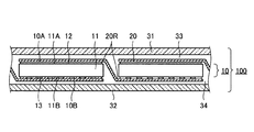
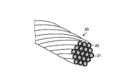
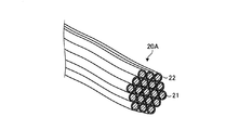
以下に、本発明の実施の形態1の太陽電池モジュールについて、図面に基づいて詳細に説明する。図1および図2は、実施の形態1の太陽電池モジュールの断面図および斜視図である。図3は、太陽電池モジュールのインターコネクタを示す斜視図である。図4は、実施の形態1のインターコネクタの太陽電池セル上での断面図、図5は、実施の形態1のインターコネクタの素子間部での断面図である。図6(a)および(b)は、実施の形態1の太陽電池モジュールに適用する太陽電池セルを表面側および裏面側から見た概略構成を示す斜視図である。図7は、実施の形態1のインターコネクタ接続工程を示す説明図である。図8は、実施の形態1のストリングの概略構成を示す斜視図、図9は、実施の形態1の太陽電池アレイの概略構成を示す斜視図である。図10は、実施の形態1の太陽電池パネルの分解斜視図、図11は、実施の形態1の太陽電池モジュールの実装工程を示すフローチャートである。実施の形態1の太陽電池モジュールは、太陽電池セル間を接続するインターコネクタ20に、図3に要部拡大斜視図を示すように、断面円形の細線状の19本の丸細線21を撚り線としたものである。なお丸細線21の外側面は、はんだ層22で被覆されている。Embodiment 1 FIG.
Below, the solar cell module of Embodiment 1 of this invention is demonstrated in detail based on drawing. 1 and 2 are a cross-sectional view and a perspective view of the solar cell module according to Embodiment 1. FIG. FIG. 3 is a perspective view showing an interconnector of the solar cell module. FIG. 4 is a cross-sectional view of the interconnector of the first embodiment on the solar battery cell, and FIG. 6 (a) and 6 (b) are perspective views showing a schematic configuration of a solar battery cell applied to the solar battery module of Embodiment 1 as viewed from the front surface side and the back surface side. FIG. 7 is an explanatory diagram illustrating an interconnector connection process according to the first embodiment. FIG. 8 is a perspective view showing a schematic configuration of the string of the first embodiment, and FIG. 9 is a perspective view showing a schematic configuration of the solar cell array of the first embodiment. FIG. 10 is an exploded perspective view of the solar cell panel of the first embodiment, and FIG. 11 is a flowchart showing a mounting process of the solar cell module of the first embodiment. In the solar cell module of Embodiment 1, the
実施の形態1の太陽電池モジュール100は、図1に示すように、pn接合を形成したp型単結晶シリコン基板で構成された半導体基板11の第1主面である受光面11A側に受光面電極12、第2主面である裏面11Bに裏面電極13を形成した太陽電池セル10をインターコネクタ20で接続したものである。太陽電池セル10は、p型シリコン基板に対して、光の集光率を高めるために受光面11A側にテクスチャエッチングにより凹凸形状を形成する。そして、図示しないn型拡散層を形成し、その上に反射防止膜であるシリコン窒化膜を成膜する。太陽電池セル10の裏面10Bには、Alを含む裏面集電電極13aおよびAgを含む裏面接合電極13bが形成され、裏面電極13を構成している。裏面集電電極13aは、開放電圧および短絡電流を向上させるための裏面電界層を有するとともに、裏面側の電流を集めるために設けられる電極であり、太陽電池セル10の裏面10Bのほぼ全域を覆う。
As shown in FIG. 1,
また、裏面接合電極13bは、インターコネクタ20と電気的に接合するために設けられる電極である。裏面接合電極13bは、インターコネクタ20を接合する方向に沿って設けられている。裏面集電電極13aおよび裏面接合電極13bは、前述したようにAl,Agなどの金属粒子を有する導電性ペーストを所望の範囲に塗布して焼成することで形成される。裏面接合電極13bは、図6(b)に示すように、インターコネクタ20を接合する方向に沿って太陽電池セル10のほぼ全長に渡って飛び石状に設けられる。なお、裏面接合電極13bは、インターコネクタ20を接合する方向に沿って太陽電池セル10のほぼ全長に渡って設けても良い。
Further, the back
太陽電池セル10の受光面10A側には、光−電子変換により発生した光電流を集める受光面集電電極である複数の受光面グリッド電極12Gと、インターコネクタ20を接合する受光面接合電極である受光面バス電極12Bとが形成されている。受光面グリッド電極12Gは、光電流を集めるための電極であり、太陽光が太陽電池セル10の内部に到達するのを妨げないようにしながら光電流を集めるために、細い直線状の電極を多数本並行に並べて形成される。
On the light-receiving
また、受光面バス電極12Bは、受光面グリッド電極12Gと直交する方向に設けられる。受光面バス電極12Bは、インターコネクタ20と電気的に接合するために設けられる電極である。受光面バス電極12Bおよび受光面グリッド電極12Gは、金属粒子を有する導電性ペーストを所望の範囲に塗布して焼成することで形成される。
The light receiving
図4および図5に示すように、インターコネクタ20は、太陽電池セル10の裏面10Bに形成された裏面接合電極13bに裏面領域がはんだ接合され、隣接する太陽電池セル10の受光面10Aに形成された受光面バス電極12Bに受光面側領域がはんだ接合される。このように、隣接する太陽電池セル10同士がインターコネクタ20によって連結されることでストリング50が形成される。
As shown in FIG. 4 and FIG. 5, the
ここで、インターコネクタ20は、太陽電池セル10の受光面バス電極12Bと、隣接する太陽電池セル10の裏面接合電極13bとを接続するために、屈曲部20Rを有する。
Here, the
インターコネクタ20は、多数の金属丸線をはんだ層で覆ったものが使用される。インターコネクタ20は、太陽電池セル10の連結方向に延びている。
The
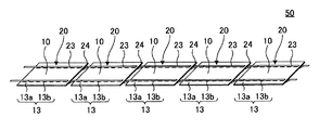
実施の形態1の太陽電池モジュール100は、インターコネクタ20をはんだ層22で被覆された丸細線21の撚り線で構成し、インターコネクタ20を用いて太陽電池セル10の第1主面10Aである受光面と第2主面10Bである裏面を交互にはんだで接続し、図8に示すようにストリング50を構成するものである。
The
図9は、本発明の実施の形態1の太陽電池アレイ70の概略構成を示す斜視図であって、裏面側から見た状態を示す。図9に示すように、複数の太陽電池セル10がインターコネクタ20で接続された太陽電池ストリング50が、さらに横タブ線25および出力タブ線26で直列に接合されて、太陽電池アレイ70が形成される。
FIG. 9 is a perspective view showing a schematic configuration of the solar cell array 70 according to Embodiment 1 of the present invention, and shows a state viewed from the back side. As shown in FIG. 9, a
図10は、図1および図2に示した太陽電池モジュールの分解斜視図である。太陽電池モジュール100は、太陽電池セル10の受光面10A側を封止する受光面側封止材33、受光面保護材31で覆い、裏面10B側を裏面側封止材34、裏面保護材32で覆い、外枠としての、補強用のフレーム40で周囲を囲んだものである。実施の形態1では、受光面側封止材33、受光面保護材31、裏面側封止材34、裏面保護材32をあわせて封止樹脂とする。
FIG. 10 is an exploded perspective view of the solar cell module shown in FIGS. 1 and 2. The
受光面10A上に形成された受光面バス電極12Bと接続したインターコネクタ20は、隣接する太陽電池セル10の裏面10B上に形成された裏面接合電極13bと接続することで、複数の太陽電池セル10を直列に接続している。
The
図1に太陽電池モジュール100の断面図を示すように、この太陽電池セル10は、厚み0.1mm以上0.2mm以下のp型単結晶シリコン基板からなる半導体基板11からなる。太陽電池セル10を構成する半導体基板11内部にはpn接合が形成され、その受光面11Aと裏面11Bには受光面バス電極12Bおよび裏面接合電極13Bが設けられ、さらに受光面11Aには反射防止膜が設けられている。太陽電池セル10の大きさは、単結晶シリコン太陽電池の場合、1辺の長さが150mm〜156mm程度である。なお、半導体基板としてはp型単結晶シリコン基板に限定されることなく、n型単結晶シリコン、多結晶シリコン基板なども適用可能である。なお図1ではpn接合も反射防止膜も図示していない。
As shown in the cross-sectional view of the
配線材としてのインターコネクタ20は、直径0.05mm程度の銅製の丸細線21表面にめっきにより形成されたはんだ層22を19本撚り合わせて形成した撚り線をなすものである。そして、図6に示すように、太陽電池セル10との接続部を構成する当接領域23と素子間部24とで構成される。当接領域23では図4に断面図を示すように、太陽電池セル10の受光面バス電極12B上では、受光面バス電極12Bよりも幅はやや大きい電極幅をもち、厚みt=0.1mm〜0.4mm程度の平角形状をなす。インターコネクタ20は、はんだ付けにより太陽電池セル10に接合され、各太陽電池セル10の受光面バス電極12Bと、隣接する太陽電池セル10の裏面接合電極13bとを電気的に接続する。そして素子間部24では図5に示すように、外径が丸線のままの撚り線を構成している。
The
裏面10B側および受光面10A側に配する裏面側封止材34および受光面側封止材33には、透光性、耐熱性、電気絶縁性、柔軟性を有する素材が用いられ、エチレンビニルアセテート(EVA)あるいはポリビニルブチラール(PVB)などの熱可塑性樹脂を主成分とする熱可塑性の合成樹脂材が好適である。なお受光面保護材31を構成する透光性基板としてはガラス板も適用可能である。厚さとしては0.4mm以上1.0mm以下のシート状形態のものが用いられる。
The back surface
裏面側封止材34および受光面側封止材33は、気圧0.5atm以上1.0atm以下の減圧下におけるラミネート工程で熱架橋し、受光面保護材31、太陽電池ストリング50、裏面保護材32と融着することで一体化がなされる。
The back surface
受光面保護材31としては、透光性、耐湿性、耐候性、耐加水分解性、絶縁性に優れた素材が用いられ、ガラス基板などの剛性の透光性基板の他、フッ素系樹脂シート、ポリエチレンテレフタレート(PET)シートなどの樹脂材が用いられる。
As the light-receiving surface
裏面保護材32としては、耐湿性、耐候性、耐加水分解性、絶縁性に優れた素材が用いられ、フッ素系樹脂シート、アルミナまたはシリカを蒸着したポリエチレンテレフタレート(PET)シートなどの樹脂材が用いられる。
As the back
ここでは、太陽電池セル10が接続されてなる太陽電池ストリング50と、受光面保護材31と、裏面保護材32と、受光面側封止材33、裏面側封止材34とを含んだものを太陽電池モジュール100としているが、これに限らず外部接続端子としてのインターコネクタ20が接合された受光面電極12と裏面電極13を有する太陽電池セル10を封止材で封止されたものも太陽電池モジュール100と呼ぶ。
Here, the
また、本実施の形態1の太陽電池セル10は概略平板状を成すが、太陽電池セル10は、平板状のものに限られるものではなく、例えば、フレキシブルなシート状、或いは立方体状などでもよく、集電電極にインターコネクタが接合される太陽電池セルであれば適用することができる。集電電極は裏面側にのみ形成されているいわゆる裏面取出し型太陽電池セルにも適用可能である。
Moreover, although the
さらに、実施の形態1の裏面接合電極13bは、太陽電池セル10の裏面10Bに2本形成されているが、2本でなくともよく、太陽電池セル10の裏面10Bに1本以上が形成されている太陽電池セルであれば適用することができる。
Furthermore, although the two back
次に、本実施の形態1の太陽電池モジュールの製造方法について説明する。図11はフローチャートである。まずステップS101で太陽電池セルを形成する。太陽電池セル10は、p型単結晶シリコン基板を出発材料とし、光の集光率を高めるために受光面11Aにテクスチャエッチングにより凹凸形状を形成し、拡散により受光面側に図示しないn型拡散層を形成しpn接合を形成すると共に、表面に反射防止膜としてのシリコン窒化膜を成膜したものである。太陽電池セル10の受光面10Aには、図6(a)に示すように、光−電子変換によって発生した電子を集める受光面バス電極12Bと受光面グリッド電極12Gからなる受光面電極12とが形成されている。
Next, a method for manufacturing the solar cell module according to Embodiment 1 will be described. FIG. 11 is a flowchart. First, a solar battery cell is formed in step S101. The
太陽電池セル10の裏面10Bには、図6(b)に示すように、Al電極からなる裏面集電電極13aとAg電極からなる裏面接合電極13bとが形成されている。裏面集電電極13aは、開放電圧および短絡電流を向上させるための裏面電界層を形成するために設けられる電極であり、太陽電池セル10の裏面の略全域を覆うように形成される。
On the
また、Ag電極からなる裏面接合電極13bは、隣接セルあるいは外部素子とコンタクトを取るために設けられる電極である。裏面集電電極13aおよび裏面接合電極13bは、金属粒子を有する導電性ペーストを所望の範囲に塗布して焼成することで形成される。実施の形態1では裏面接合電極13bをスクリーン印刷により形成した後、裏面集電電極13aとしてのAl電極を形成する。
Further, the
図6(a)に受光面側、図6(b)に裏面側を示すように、ステップS102に示すように、太陽電池セル10にインターコネクタ20を配し、加熱によりはんだ接合を行い、固着する。
As shown in step S102, as shown in FIG. 6A on the light receiving surface side and in FIG. 6B on the back surface side, the
図7は、本発明の実施の形態1の受光面電極12および裏面電極13とインターコネクタ20とを電気的に接合するインターコネクタ接合工程を示すものである。図7に示すように、太陽電池セル10の裏面接合電極13bにインターコネクタ20の裏面側の当接領域23を重ね、受光面バス電極12Bにインターコネクタ20の接合領域23を重ねた状態で、ヒートツール200で加熱することで、インターコネクタ20と裏面接合電極13bとの電気的接合およびインターコネクタ20と受光面バス電極12Bとの電気的接合が同時に確保できる。
FIG. 7 shows an interconnector joining step for electrically joining the light receiving
なお、インターコネクタ接合工程では、裏面側の接合工程と受光面側の接合工程を分けて、2回の工程で実施してもよい。 In the interconnector joining step, the joining step on the back surface side and the joining step on the light receiving surface side may be divided and performed in two steps.
図8は、実施の形態1にかかる方法で太陽電池セル10を仮着した太陽電池ストリング50の概略構成を示す斜視図である。図8に示すように、複数の太陽電池セル10が併設され、インターコネクタ20で直列に接続されて、太陽電池ストリング50が形成される。すなわち、インターコネクタ20は、太陽電池セル10の裏面10Bに形成された裏面接合電極13bにその一端側の当接領域23がはんだ接合され、隣接する太陽電池セル10の受光面10Aに形成された受光面バス電極12Bに他端側の当接領域23がはんだ接合される。このように、隣接する太陽電池セル10同士がインターコネクタ20によって連結されることで太陽電池ストリング50が形成される。
FIG. 8 is a perspective view showing a schematic configuration of the
インターコネクタ20は、銅線を延伸加工して予め決められた直径とし、はんだ槽に浸漬してはんだコートを施したはんだ被覆の丸細線21を撚り加工して形成した撚り線が使用される。インターコネクタ20は、平面視において太陽電池セル10の連結方向に延び、略長方形形状を呈している。
The
また、実施の形態1におけるはんだ層として、In系の低融点無鉛はんだ、Bi系無鉛はんだなど、封止材の硬化温度よりも低融点のはんだを用いることで、積層体の形成後、1回の熱処理で一括して固着することができる。これは、封止材の硬化温度で、はんだが溶融するため、ラミネート工程における加熱で同時にはんだ接合が可能であるためである。例としては、Bi系はんだであるSn−58Biの融点が138℃、Sn−58Bi−1Agの融点が137℃、In系はんだであるSn−52Inの融点が117℃として挙げられ、Sn−Ag−Cu系はんだの融点227℃と比較しても、低温でのはんだ接合が可能である。なお、ここで示すBiおよびInの含有率は一例であり、本実施の形態を特定するものではなく、低融点無鉛はんだの融点は、ラミネート工程における樹脂の溶融温度以下であればよい。 Further, as the solder layer in the first embodiment, by using a solder having a melting point lower than the curing temperature of the sealing material, such as an In-based low melting point lead-free solder or a Bi-based lead-free solder, once the laminated body is formed, Can be fixed together by heat treatment. This is because the solder melts at the curing temperature of the sealing material, so that soldering can be performed simultaneously by heating in the laminating process. For example, the melting point of Sn-58Bi that is Bi-based solder is 138 ° C., the melting point of Sn-58Bi-1Ag is 137 ° C., the melting point of Sn-52In that is In-based solder is 117 ° C., Sn—Ag— Even when compared with a melting point of 227 ° C. of Cu-based solder, solder bonding at a low temperature is possible. Note that the contents of Bi and In shown here are merely examples and do not specify the present embodiment, and the melting point of the low melting point lead-free solder may be equal to or lower than the melting temperature of the resin in the laminating step.
実施の形態3で後述するように、一括熱処理によって固着する場合には、裏面接合電極13b上からインターコネクタ20がずれる可能性があるため、仮止めテープのようなもので仮固定しておくのが望ましい。なお、ずれるおそれがない場合は、仮固定は不要であり、配置するだけでもよい。
As will be described later in the third embodiment, when fixing by batch heat treatment, the
図9は、以上のようにして得られた複数の太陽電池ストリング50を横タブ線25で接続した太陽電池アレイ70の概略構成を示す斜視図である。太陽電池アレイ70は、並列に配置した複数の太陽電池ストリング50を横タブ線25としてのバスバーを用いて直列に接続し、電力取り出し用の出力タブ線26としてのバスバーを設置することで形成される。
FIG. 9 is a perspective view showing a schematic configuration of a solar cell array 70 in which a plurality of solar cell strings 50 obtained as described above are connected by
このようにして得られた太陽電池アレイ70の受光面側に、図10に示すように、ステップS103で受光面側封止材33、受光面保護材31、裏面側に裏面側封止材34、裏面保護材32を配し、積層体を形成する。
As shown in FIG. 10, on the light receiving surface side of the solar cell array 70 thus obtained, in step S103, the light receiving surface
この状態で積層体をラミネート装置に装着し、ステップS104において140℃以上160℃以下で30分前後の熱処理を行うことで、ステップS105に示す太陽電池モジュールを形成する。 In this state, the laminate is mounted on a laminating apparatus, and heat treatment is performed at 140 ° C. to 160 ° C. for about 30 minutes in step S104, thereby forming the solar cell module shown in step S105.
実施の形態1のインターコネクタ20によれば、図3に示したように、束状の撚り線を構成している。インターコネクタ20は、図3に示すようにはんだめっきされた丸細線21を複数本束ね、さらにその束を撚っている。そのためはんだ層22で被覆された丸細線21一本一本は螺旋状になっている。このため、インターコネクタ20自体が、弾性を有しており、太陽電池セル10の裏面10B側と受光面10A側とを接続する際、基板厚さに起因する段差によって曲げ部が形成されるが、曲げ部による応力は撚り線によって緩和される。従って、接合時における、インターコネクタ20近辺の過剰な温度ストレスに起因する応力に対しては撚り線が緩衝材となって応力を緩和することができる。またインターコネクタと太陽電池セルの集電電極との接合の際にかかる温度ストレスを最小限に抑えることで、太陽電池セルに発生するクラックを防止することもできる。
According to the
インターコネクタ20は、延伸加工によって、容易に所望の径を有する丸細線21を材料としているため、加工費が少なくて済み、丸線から平角線を形成する場合に比べて材料の無駄がなく、コストの低減をはかることができる。また、受光面電極および裏面電極との当接領域において、接触面積が大きく、接合強度が大幅に向上する。
Since the
また、一般的に、太陽電池モジュールは、太陽電池セル10、受光面側封止材33、受光面保護材31、裏面側に裏面側封止材34、裏面保護材32、インターコネクタ20等の、熱膨張係数の異なる構成要素で構成されている。従って、太陽電池モジュール105の温度が気温の影響あるいは動作時の発熱の影響などで温度変化すると、各構成要素には温度変化に伴う体積変化の差異により応力が発生する。特に、太陽電池モジュール10の構成要素の中で、図1で示したインターコネクタ20の屈曲部20Rに歪が集中し、太陽電池モジュールの使用時に繰り返し発生する応力によって、屈曲部20Rが最初に破壊することが知られている。
In general, the solar cell module includes a
これに対し、実施の形態1の太陽電池モジュール100はインターコネクタ20に束状の撚り線を用いている。インターコネクタ20を構成するはんだ層22で被覆された丸細線21は螺旋状になっており、弾性を有しており伸縮する余裕がある。このため、太陽電池モジュール100の構成要素の熱膨張係数に違いがあっても、インターコネクタ20の伸縮により温度変化に伴う体積変化の差異を緩和できるので、温度変化によって屈曲部20Rに発生する応力は低減する。応力の低減により、信頼性に優れた太陽電池モジュールを得ることができる。
On the other hand, the
また束状の撚り線からなるインターコネクタ20の断面の形状は、通常は図3のように丸細線21の束になっているため概ね円形状となっている。しかし、太陽電池セル10の受光面電極12とインターコネクタ20をヒートツール200で加熱して接合する際に、インターコネクタ20を押さえで押さえることによって、インターコネクタ20は同じ断面積を有する1本の丸線インターコネクタと比較して、平角線並にセル受光面電極との接合面積を確保し、かつインターコネクタ20の全体高さを平角線並に維持する、つまり、残留熱応力を平角線並に維持することができる。
In addition, the cross-sectional shape of the
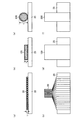
図12に、インターコネクタ20と丸線インターコネクタ1本のそれぞれの場合における、横タブ線との接合状態の違いを当接領域断面模式図にて示す。(a)および(b)は、実施の形態1の撚り線からなるインターコネクタ20を用いた場合の横タブ線25との接続状態を示す断面図、及び上面図である。(c)および(d)は、平角導体からなるインターコネクタ120を用いた場合の横タブ線25との接続状態を示す断面図、および上面図である。(e)および(f)は、丸線からなるインターコネクタ220を用いた場合の横タブ線25との接続状態を示す断面図、および上面図である。
FIG. 12 is a contact area cross-sectional schematic diagram showing the difference in joining state between the horizontal tab line and the
インターコネクタ20と横タブ線25との接合においては、実施の形態1の場合、インターコネクタ20を押さえで押さえることによって、束状インターコネクタの方が、同断面積を有する1本の丸線からなるインターコネクタ220と比較して、接合面積が大きく、かつ、インターコネクタ20の高さが低い、すなわち他部材との絶縁距離が長くなる。平角導体からなるインターコネクタ120と比較した場合においても効果がある。
In the joining of the
以上説明してきたように実施の形態1の太陽電池モジュールによれば、丸線を用いてインターコネクタの加工費を低減しながら、太陽電池モジュールの構成要素の熱膨張係数の違いにより温度変化によって素子間の段差部に発生する応力を低減することができる。またセルとの接合面積を確保し、かつインターコネクタの厚みを平角線並に維持することができる。また、残留熱応力を平角線よりも小さくすることができる。 As described above, according to the solar cell module of the first embodiment, the element due to the temperature change due to the difference in the thermal expansion coefficient of the components of the solar cell module while reducing the processing cost of the interconnector using the round wire. It is possible to reduce the stress generated in the step portion between them. Further, it is possible to secure a bonding area with the cell and maintain the thickness of the interconnector as a flat wire. Further, the residual thermal stress can be made smaller than that of the rectangular wire.
なお、実施の形態1では、太陽電池セル10との接続部においてのみ、図4に示したようにインターコネクタ20の外形が四角形となるようにし、その他の領域では、図5に示したように丸細線の集合体として形成したが、全体にわたって断面四角形となるようにしてもよい。全体にわたって断面四角形となるようにすることで、実施の形態1による効果に加え、通例の平角導体用の装置をそのまま使用することができるという効果を奏する。
In the first embodiment, the outer shape of the
また、全体にわたって図5に示したように丸細線の束状体として形成してもよい。全体にわたって丸細線の束状体とすることで、実施の形態1による効果に加え、弾性力が大きく、インターコネクタ20と太陽電池セル10との当接領域においてさらなる緩衝効果を得ることができるという効果を奏する。
Further, as shown in FIG. 5 as a whole, it may be formed as a bundle of round thin wires. By forming a bundle of round thin wires throughout, in addition to the effect of the first embodiment, the elastic force is large, and a further buffering effect can be obtained in the contact region between the interconnector 20 and the
加えて、横タブ線25との当接領域で、インターコネクタ20は、丸細線が横並びに配列され、他の領域での断面の幅よりも広い四角形を構成している。このため、横タブ線25との接続が強固で、より信頼性の高いものとなっている。
In addition, in the contact area with the
また、インターコネクタは、太陽電池セルの第1電極から、隣接する太陽電池セルの第2電極に伸びるが、撚り線で構成されているため、曲げ部に応力が残留するのを回避することができ、信頼性の高い接続が可能となる。 In addition, the interconnector extends from the first electrode of the solar battery cell to the second electrode of the adjacent solar battery cell. However, since the interconnector is formed of a stranded wire, it is possible to avoid stress remaining in the bent portion. And a highly reliable connection is possible.
また、第1電極および第2電極との当接領域における、インターコネクタの外形は、第1電極および第2電極の幅と同一幅とすることで、受光面積を小さくすることなく、第1および第2電極とインターコネクタとの強固な接続が可能となる。特に第1電極および第2電極との当接領域における、インターコネクタの外形は、断面四角形であるのが望ましい。また電極および隣接する太陽電池セルの第2電極との間に位置する素子間部における、インターコネクタの外形は、断面円形であるため、より弾性が大きく緩衝効果が高いため、インターコネクタの曲げ部での残留応力の低減を図ることが可能となる。 In addition, the outer shape of the interconnector in the contact area between the first electrode and the second electrode is the same as the width of the first electrode and the second electrode, so that the first and second light receiving areas are not reduced. A strong connection between the second electrode and the interconnector is possible. In particular, the outer shape of the interconnector in the contact area between the first electrode and the second electrode is preferably a square in cross section. In addition, since the outer shape of the interconnector in the inter-element portion located between the electrode and the second electrode of the adjacent solar battery cell is circular in cross section, it is more elastic and has a higher buffering effect. It is possible to reduce the residual stress at.
インターコネクタは、太陽電池セルの外では、太陽電池セル上よりも幅広となっているため、封止樹脂との接触面積が大きく、封止樹脂との接合強度を高めることが可能となる。 Since the interconnector is wider outside the solar battery cell than on the solar battery cell, the interconnector has a large contact area with the sealing resin and can increase the bonding strength with the sealing resin.
また、インターコネクタは、前記太陽電池セルの外では、丸細線が一列に配列されて横タブ線に接続されているため、接続強度を高めることができる。 Moreover, since the interconnector is connected to the horizontal tab line outside the solar battery cell, the round thin lines are arranged in a line, the connection strength can be increased.
実施の形態2.
次に、実施の形態2の太陽電池モジュールについて、図面に基づいて詳細に説明する。図13は、実施の形態2の太陽電池モジュールのインターコネクタを示す斜視図である。実施の形態1のインターコネクタ20は丸細線21の撚り線で構成したが、実施の形態2のインターコネクタ20Aははんだ層22で被覆された丸細線21を撚り線とすることなく、束状にして用いられる。つまり、実施の形態2のインターコネクタ20Aは、撚りを形成しない、並行する複数の丸細線で形成される。他の構成については前記実施の形態のインターコネクタと同様である。インターコネクタ以外については、実施の形態1の太陽電池モジュールと同様であるためここでは説明を省略する。同一部位には同一符号を付した。
Next, the solar cell module of
以上説明してきたように実施の形態2の太陽電池モジュールによれば、撚り線を構成することなく、19本の丸細線を束ねているため、接合時に電極上での形状を変更し、下層の電極形状に合わせたインターコネクタ形状を得ることが可能となる。また、実施の形態1の太陽電池モジュールと同様、丸線を用いてインターコネクタの加工費を低減しながら、太陽電池モジュールの構成要素の熱膨張係数の違いにより温度変化によって素子間部24に発生する応力を低減し、またセルとの接合面積を確保し、かつインターコネクタの厚みを平角線並に維持、つまり、残留熱応力を平角線並に維持することができる。
As described above, according to the solar cell module of
実施の形態3.
次に、実施の形態3の太陽電池モジュールについて、図面に基づいて詳細に説明する。実施の形態3では、太陽電池モジュールの製造工程において、図14にフローチャートを示すように、太陽電池セルに封止材の硬化温度よりも低融点を持つ低融点はんだを介してインターコネクタ20Bを仮配置し、インターコネクタ20Bが仮配置された太陽電池を、封止材とともに積層し、一括熱処理工程で、太陽電池セルにインターコネクタをはんだ接合するとともに、封止材を熱硬化させる工程とを含むことを特徴とする。Embodiment 3 FIG.
Next, the solar cell module of Embodiment 3 is demonstrated in detail based on drawing. In the third embodiment, in the solar cell module manufacturing process, as shown in the flowchart in FIG. 14, the
図15に、太陽電池セル10上の受光面電極12上のインターコネクタ20Bを示すように、実施の形態1と異なり、受光面電極12上では撚線のままの形状を有している点で実施の形態1の太陽電池モジュールと異なる。図1と同様であるため、全体図としての図示は省略するが、実施の形態3の太陽電池モジュール100は、図1に示したのと同様インターコネクタ20Bをはんだ層22で被覆された丸細線21の撚り線で構成し、太陽電池セル10間の接続に低融点無鉛はんだを用い、受光面保護材31および裏面保護材32を用いたラミネート処理工程で、一括してはんだ接続を行う。複数の太陽電池セル10の第1主面である受光面10Aと第2主面である裏面10Bを交互にインターコネクタ20Bを用いて低融点無鉛はんだで接続した太陽電池ストリング50の受光面10A側に受光面保護材31を配置し、裏面10B側に裏面保護材32を配置し、太陽電池ストリング50と受光面保護材31及び裏面保護材32の間にそれぞれ受光面側封止材33、裏面側封止材34を配置することで構成されている。
As shown in FIG. 15, the
また、実施の形態3におけるはんだ層としては、In系の低融点無鉛はんだ、Bi系無鉛はんだなど、封止材の硬化温度よりも低融点のはんだを用い、積層体の形成後、1回の熱処理で一括固着するものである。これは、封止材の硬化温度で、はんだが溶融するため、ラミネート工程における加熱で同時にはんだ接合が可能であるためである。例としては、Bi系はんだであるSn−58Biの融点が138℃、Sn−58Bi−1Agの融点が137℃、In系はんだであるSn−52Inの融点が117℃として挙げられ、Sn−Ag−Cu系はんだの融点227℃と比較しても、低温でのはんだ接合が可能である。なお、ここで示すBiおよびInの含有率は一例であり、本実施の形態を特定するものではなく、低融点無鉛はんだの融点は、ラミネート工程における樹脂の溶融温度以下であればよい。 Further, as the solder layer in the third embodiment, a solder having a melting point lower than the curing temperature of the sealing material, such as an In-based low melting point lead-free solder or a Bi-based lead-free solder, is used once after the formation of the laminate. It is fixed together by heat treatment. This is because the solder melts at the curing temperature of the sealing material, so that soldering can be performed simultaneously by heating in the laminating process. For example, the melting point of Sn-58Bi that is Bi-based solder is 138 ° C., the melting point of Sn-58Bi-1Ag is 137 ° C., the melting point of Sn-52In that is In-based solder is 117 ° C., Sn—Ag— Even when compared with a melting point of 227 ° C. of Cu-based solder, solder bonding at a low temperature is possible. Note that the contents of Bi and In shown here are merely examples and do not specify the present embodiment, and the melting point of the low melting point lead-free solder may be equal to or lower than the melting temperature of the resin in the laminating step.
本実施の形態ではインターコネクタ20の固着ステップS102に代えて、仮止めテープを用いて仮固着ステップS102Sを行う。
In the present embodiment, the temporary fixing step S102S is performed using a temporary fixing tape instead of the fixing step S102 of the
図9は、以上のようにして得られた複数の太陽電池ストリング50を横タブ線25で接続した太陽電池アレイ70は、並列に配置した複数の太陽電池ストリング50を横タブ線25としてのバスバーを用いて直列に接続し、電力取り出し用の出力タブ線26としてのバスバーを設置することで形成される。
FIG. 9 shows a solar cell array 70 in which a plurality of solar cell strings 50 obtained as described above are connected by horizontal tab lines 25. The solar cell array 70 includes a plurality of solar cell strings 50 arranged in parallel as
以上のようにして得られた太陽電池アレイ70の受光面側に、図10に示すように、ステップS103で受光面側封止材33、受光面保護材31、裏面側に裏面側封止材34、裏面保護材32を配し、積層体を形成する。
On the light receiving surface side of the solar cell array 70 obtained as described above, as shown in FIG. 10, in step S103, the light receiving surface
この状態で積層体をラミネート装置に装着し、ステップS104Sにおいて140℃以上160℃以下で30分前後の一括熱処理を行うことで、インターコネクタ20の接続とラミネート処理とを同時に行い、ステップS105に示す太陽電池モジュールを形成する。
In this state, the laminated body is mounted on the laminating apparatus, and the
ラミネート温度T0は140℃以上160℃以下、キュア温度T1は130℃以上155℃以下、キュア後からT2常温の各工程30分前後をかけて処理するのが一般的であり半田融点t℃以上で半田が溶融、半田融点t℃以下で凝固し、電気的接合が可能となる。Laminating temperature T 0 is 140 ° C. or higher 160 ° C. or less, curing temperature T 1 of the 130 ° C. or higher 155 ° C. or less, it is common to process later cured over T 2 ambient temperature each step 30 minutes before and after the solder melting point t Solder melts at a temperature higher than or equal to ℃ and solidifies at a solder melting point of less than or equal to t ℃, allowing electrical bonding.
これにより、製造にかかるタクトを短縮するのみでなく製造コストを低減させることができる。また、1度の熱ストレスのみで太陽電池モジュールの製造が可能となり、太陽電池セルにかかる熱ストレスの低減による太陽電池セルのクラック対策および長期信頼性を向上させることができる。なお、上記にかかるラミネート加工条件あるいはプロセスは一例であり、本発明を特定するものではない。 Thereby, not only the tact time concerning manufacture can be shortened but also the manufacturing cost can be reduced. Moreover, a solar cell module can be manufactured only with one thermal stress, and the crack countermeasure and long-term reliability of the solar cell can be improved by reducing the thermal stress applied to the solar cell. In addition, the lamination process conditions or process concerning the above are examples, and do not specify this invention.
さらに、本実施の形態3の太陽電池モジュールの製造方法によれば、受光面保護材および裏面保護材と共に加熱されるため良好な支持がなされつつラミネート加工およびはんだ接合が実現されるため、近年の太陽電池ウエハの薄肉化の課題であったはんだ接合時の熱応力低減にも、効力を発揮し、太陽電池セルの直材費低減にも繋げることができる。 Furthermore, according to the manufacturing method of the solar cell module of the third embodiment, since it is heated together with the light-receiving surface protection material and the back surface protection material, laminating and solder bonding are realized while being supported favorably. It is effective for reducing thermal stress at the time of soldering, which has been a problem of thinning the solar battery wafer, and can also lead to a reduction in the direct material cost of the solar battery cell.
このようにして形成された、本実施の形態3にかかる太陽電池モジュールは、太陽電池セルを直列に接続して太陽電池ストリングをなすインターコネクタとを封止する工程で、インターコネクタと受光面集電電極および裏面集電電極とのはんだ接合を同時に行なう一括熱処理工程により形成されたことを特徴とする。従って、並列に配置した複数の太陽電池ストリングを直列接続して太陽電池アレイを形成する横タブ線25と、太陽電池アレイから電力を取り出す出力タブ線26とを備えた構造となっている。
The solar cell module according to the third embodiment formed in this way is a step of sealing the interconnector forming the solar cell string by connecting the solar cells in series, and the interconnector and the light receiving surface collection. It is characterized in that it is formed by a collective heat treatment process in which soldering of the electric electrode and the back surface collecting electrode is performed simultaneously. Therefore, it has a structure including a
なお、インターコネクタ20Bと受光面バス電極12Bおよび裏面接合電極13bとのはんだ接合と同時に樹脂封止がなされるため、撚り線からなるインターコネクタ20Bのはんだ接合部の周縁に、樹脂が入り込み、なじみあって強固な接合状態を形成している。また樹脂封止に先立ち、インターコネクタと受光面バス電極および裏面接合電極とのはんだ接合を行う場合、クランプなどの押圧治具によりインターコネクタを押圧するため、チップクラックが生じたり、インターコネクタにクランプ跡が残ったりすることがある。これに対し、本実施の形態1の方法では、薄い太陽電池セルの場合にも両面を保護しつつ押圧してはんだ接合がなされるため、生産性が良好であるだけでなく、チップクラックや、インターコネクタのクランプ跡などもなく外観性に優れ製造歩留まりの向上をはかることができる。
In addition, since resin sealing is performed simultaneously with solder joining of the
以上のように、本実施の形態3にかかる太陽電池モジュールの製造方法によれば、複数の太陽電池セルと、太陽電池セル同士を接続するIn系の低融点無鉛はんだではんだコートされたインターコネクタとを有し、複数の太陽電池セルをインターコネクタで直列に接続した複数の太陽電池ストリングと、並列に配置された複数の太陽電池ストリングと、複数の太陽電池ストリングを直列に接続するバスバーすなわち横タブ線とを有する太陽電池アレイと、太陽電池アレイにおいて集電された電力を太陽電池アレイから出力を取り出すバスバーすなわち出力タブ線と、を備え、インターコネクタおよびバスバーの電気的接合をラミネート工程で一括して行うことを特徴とする。 As described above, according to the method for manufacturing a solar cell module according to the third embodiment, a plurality of solar cells and an interconnector solder-coated with an In-based low melting point lead-free solder that connects the solar cells to each other. A plurality of solar cell strings in which a plurality of solar cells are connected in series with an interconnector, a plurality of solar cell strings arranged in parallel, and a bus bar that connects the plurality of solar cell strings in series A solar cell array having a tab wire, and a bus bar or output tab wire for taking out the output of the power collected in the solar cell array from the solar cell array. It is characterized by being performed.
実施の形態3の太陽電池モジュールの製造方法によれば、太陽電池セル10に丸細線の撚り線からなるインターコネクタ20Bをはんだ接合する熱処理工程を、封止用の樹脂とともに一括熱処理を行うことで実施する。これにより、太陽電池セル10は封止材で保護された状態で熱処理が施されるため、太陽電池モジュールにかかる温度ストレスを最小限に抑えるとともに、太陽電池セルが薄くなったとしても長期信頼性を高めることができるという効果を奏する。
According to the method for manufacturing the solar cell module of the third embodiment, the heat treatment step for solder-bonding the
なお、実施の形態1から3では、太陽電池セルにインターコネクタをはんだ接合して太陽電池ストリングを形成する例について説明したが、1個の太陽電池セルに電流取り出し用の配線材としてインターコネクタを用いる場合にも適用可能であることはいうまでもない。 In the first to third embodiments, an example in which an interconnector is soldered to a solar battery cell to form a solar battery string has been described. However, an interconnector is used as a wiring material for extracting current in one solar battery cell. Needless to say, the present invention can also be applied to the case of use.
また、太陽電池セルについては、実施の形態1から3で用いた両面取出し型の太陽電池に限定されることなく、1方の面のみから電流取出しを行うタイプの太陽電池、電流取出し位置についても、コーナー部など適宜変更可能であることは言うまでもない。太陽電池セルにインターコネクタをはんだ接合して太陽電池ストリングを形成する例について説明したが、1個の太陽電池セルに電流取り出し用の配線材としてインターコネクタを用いる場合にも適用可能であることはいうまでもない。 In addition, the solar battery cell is not limited to the double-sided extraction type solar battery used in the first to third embodiments, but is also a type of solar battery that performs current extraction from only one surface and the current extraction position. Needless to say, the corner portion can be appropriately changed. Although an example in which an interconnector is soldered to a solar battery cell to form a solar battery string has been described, it can be applied to a case where an interconnector is used as a wiring material for extracting current in one solar battery cell. Needless to say.
また、上記実施の形態1から3では、太陽電池セルとして多結晶シリコンや単結晶シリコンなどの結晶系太陽電池を使用したものについて説明してきたが、薄膜系太陽電池や有機系太陽電池などの結晶系でない太陽電池セルでも適用可能である。 In the first to third embodiments, the solar cell is described using a crystalline solar cell such as polycrystalline silicon or single crystal silicon. However, a crystal such as a thin film solar cell or an organic solar cell is used. It can also be applied to non-system solar cells.
10 太陽電池セル、10A 受光面、10B 裏面、11 半導体基板、11A 受光面、11B 裏面、12 受光面電極、12G 受光面グリッド電極、12B 受光面バス電極、13a 裏面集電電極、13b 裏面接合電極、20,20A インターコネクタ、20R 屈曲部、21 丸細線、22 はんだ層、23 当接領域、24 素子間部、25 横タブ線、26 出力タブ線、31 受光面保護材、32 裏面保護材、33 受光面側封止材、34 裏面側封止材、40 フレーム、50 太陽電池ストリング、70 太陽電池アレイ、100 太陽電池モジュール、200 ヒートツール。
DESCRIPTION OF
Claims (3)
前記第1電極と隣接する太陽電池セルの第2電極との当接領域を有し、前記太陽電池セルと前記隣接する太陽電池セルとの間を接続するインターコネクタとを備え、
前記インターコネクタが、複数の丸細線からなる束状体であり、
前記インターコネクタは、前記太陽電池セルの外で前記インターコネクタに接続される横タブ線との接続領域で、前記太陽電池セル上よりも幅が広くなっており、
前記インターコネクタは、前記第1電極および隣接する前記太陽電池セルの前記第2電極との間に位置する素子間部では、前記太陽電池セル上よりも幅が狭くなっていることを特徴とする太陽電池モジュール。 a solar cell comprising a semiconductor substrate having a pn junction, and a first electrode and a second electrode formed in a p-type region and an n-type region of the semiconductor substrate;
The first electrode and the second electrode of the adjacent solar battery cell has a contact region, and includes an interconnector that connects between the solar battery cell and the adjacent solar battery cell,
The interconnector is a bundle of a plurality of round thin wires,
The interconnector is wider than the solar cell on the connection region with the horizontal tab line connected to the interconnector outside the solar cell ,
The interconnector is narrower in width between the first electrode and the second electrode of the adjacent solar battery cell than on the solar battery cell. Solar cell module.
前記第1電極と隣接する太陽電池セルの第2電極との当接領域を有し、前記太陽電池セルと前記隣接する太陽電池セルとの間を接続するインターコネクタとを備え、
前記インターコネクタが、複数の丸細線からなる束状体であり、
前記インターコネクタは、前記太陽電池セルの外では、前記丸細線が一列に配列されて前記インターコネクタに直交する横タブ線に接続され、
前記インターコネクタは、前記第1電極および隣接する前記太陽電池セルの前記第2電極との間に位置する素子間部では、前記太陽電池セル上よりも幅が狭くなっていることを特徴とする太陽電池モジュール。 a solar cell comprising a semiconductor substrate having a pn junction, and a first electrode and a second electrode formed in a p-type region and an n-type region of the semiconductor substrate;
The first electrode and the second electrode of the adjacent solar battery cell has a contact region, and includes an interconnector that connects between the solar battery cell and the adjacent solar battery cell,
The interconnector is a bundle of a plurality of round thin wires,
The interconnector is connected to a lateral tab line orthogonal to the interconnector, with the round thin wires arranged in a row outside the solar cells ,
The interconnector is narrower in width between the first electrode and the second electrode of the adjacent solar battery cell than on the solar battery cell. Solar cell module.
前記第1電極および隣接する前記太陽電池セルの前記第2電極との間に位置する素子間部における、前記インターコネクタの外形は、断面円形であることを特徴とする請求項1または2に記載の太陽電池モジュール。 The outer shape of the interconnector in the contact region between the first electrode and the second electrode is the same width as the width of the first electrode and the second electrode,
The inter-element portion located between the second electrode of the solar cell to the first electrode and the adjacent, outer shape of the interconnector according to claim 1 or 2, characterized in that a circular cross-section Solar cell module.
Applications Claiming Priority (1)
| Application Number | Priority Date | Filing Date | Title |
|---|---|---|---|
| PCT/JP2015/070189 WO2017009957A1 (en) | 2015-07-14 | 2015-07-14 | Solar battery module and manufacturing method for solar battery module |
Related Child Applications (1)
| Application Number | Title | Priority Date | Filing Date |
|---|---|---|---|
| JP2018160326A Division JP6639589B2 (en) | 2018-08-29 | 2018-08-29 | Solar cell module and method of manufacturing solar cell module |
Publications (2)
| Publication Number | Publication Date |
|---|---|
| JPWO2017009957A1 JPWO2017009957A1 (en) | 2017-11-09 |
| JP6448792B2 true JP6448792B2 (en) | 2019-01-09 |
Family
ID=57757078
Family Applications (1)
| Application Number | Title | Priority Date | Filing Date |
|---|---|---|---|
| JP2017528060A Expired - Fee Related JP6448792B2 (en) | 2015-07-14 | 2015-07-14 | Solar cell module and method for manufacturing solar cell module |
Country Status (3)
| Country | Link |
|---|---|
| US (1) | US10418503B2 (en) |
| JP (1) | JP6448792B2 (en) |
| WO (1) | WO2017009957A1 (en) |
Families Citing this family (4)
| Publication number | Priority date | Publication date | Assignee | Title |
|---|---|---|---|---|
| KR101751946B1 (en) * | 2015-12-28 | 2017-06-28 | 엘지전자 주식회사 | Solar cell module |
| WO2018180922A1 (en) * | 2017-03-28 | 2018-10-04 | 株式会社カネカ | Solar cell module and manufacturing method thereof |
| WO2019163778A1 (en) * | 2018-02-21 | 2019-08-29 | 株式会社カネカ | Wiring material, solar cell using same, and solar cell module |
| DE102021119776A1 (en) | 2021-07-29 | 2023-02-02 | Hanwha Q Cells Gmbh | Multi-core connection connector for photovoltaic modules |
Family Cites Families (13)
| Publication number | Priority date | Publication date | Assignee | Title |
|---|---|---|---|---|
| JPH11177117A (en) * | 1997-12-12 | 1999-07-02 | Showa Shell Sekiyu Kk | Solar battery module |
| JP3683700B2 (en) * | 1998-02-27 | 2005-08-17 | 京セラ株式会社 | Solar cell device |
| JP2005072115A (en) | 2003-08-21 | 2005-03-17 | Sekisui Jushi Co Ltd | Solar cell module |
| JP2005191116A (en) | 2003-12-24 | 2005-07-14 | Kyocera Corp | Inner lead for connecting solar cell element and solar cell module |
| JP4792713B2 (en) * | 2004-06-14 | 2011-10-12 | 日立電線株式会社 | Lead wire, manufacturing method thereof, and solar cell assembly |
| JP2008252051A (en) | 2007-03-02 | 2008-10-16 | Sanyo Electric Co Ltd | Solar cell module |
| JP5820976B2 (en) | 2008-07-31 | 2015-11-24 | パナソニックIpマネジメント株式会社 | Manufacturing method of solar cell module |
| JP2012129359A (en) | 2010-12-15 | 2012-07-05 | Mitsubishi Electric Corp | Solar cell module and solar cell |
| JP6065646B2 (en) * | 2012-02-29 | 2017-01-25 | 新日鐵住金株式会社 | Tape-like conductive material, solar cell interconnector and solar cell module |
| ES2533574T3 (en) * | 2012-05-04 | 2015-04-13 | Sol Invictus Energy | Hybrid woven materials useful in the production of posterior contact solar cells |
| JP2014041940A (en) | 2012-08-23 | 2014-03-06 | Mitsubishi Electric Corp | Solar cell module |
| JP6280692B2 (en) | 2013-03-21 | 2018-02-14 | デクセリアルズ株式会社 | SOLAR CELL MODULE AND CRYSTAL SOLAR CELL MODULE MANUFACTURING METHOD |
| EP3235012B1 (en) * | 2014-12-15 | 2022-01-26 | IMEC vzw | Method for interconnecting back-contact photovoltaic cells |
-
2015
- 2015-07-14 US US15/569,160 patent/US10418503B2/en not_active Expired - Fee Related
- 2015-07-14 WO PCT/JP2015/070189 patent/WO2017009957A1/en active Application Filing
- 2015-07-14 JP JP2017528060A patent/JP6448792B2/en not_active Expired - Fee Related
Also Published As
| Publication number | Publication date |
|---|---|
| JPWO2017009957A1 (en) | 2017-11-09 |
| WO2017009957A1 (en) | 2017-01-19 |
| US10418503B2 (en) | 2019-09-17 |
| US20180151768A1 (en) | 2018-05-31 |
Similar Documents
| Publication | Publication Date | Title |
|---|---|---|
| US11538952B2 (en) | Solar cell module and method for manufacturing the same | |
| KR101679452B1 (en) | Solar battery, solar battery module and solar battery system | |
| US20110048492A1 (en) | Solar cell and solar cell module | |
| US10825938B2 (en) | Solar cell module | |
| JP5879513B2 (en) | Solar cell module | |
| KR20120010251A (en) | Wiring sheet, solar cell provided with wiring sheet, and solar cell module | |
| JP6448792B2 (en) | Solar cell module and method for manufacturing solar cell module | |
| JP5203176B2 (en) | Wiring sheet, solar cell with wiring sheet and solar cell module | |
| JP6163014B2 (en) | Manufacturing method of solar cell module | |
| CN109560147B (en) | Solar cell panel | |
| US20190379321A1 (en) | Solar roof tile connectors | |
| JP6639589B2 (en) | Solar cell module and method of manufacturing solar cell module | |
| JP5381809B2 (en) | Solar cell module | |
| JP2006278695A (en) | Solar cell module | |
| JP5174972B2 (en) | Thin film solar cell module and manufacturing method thereof | |
| WO2019159255A1 (en) | Method for manufacturing solar cell module | |
| JP6602242B2 (en) | Solar cell module | |
| TWI680586B (en) | Solar battery module | |
| WO2020054020A1 (en) | Solar cell connection tab, solar cell connection tab manufacturing apparatus, method for manufacturing solar cell connection tab, and solar cell module | |
| JP2017143311A (en) | Method of manufacturing solar battery module | |
| JP5382150B2 (en) | Solar cell module | |
| WO2017056363A1 (en) | Method for producing solar cell module |
Legal Events
| Date | Code | Title | Description |
|---|---|---|---|
| A521 | Request for written amendment filed |
Free format text: JAPANESE INTERMEDIATE CODE: A523 Effective date: 20170725 |
|
| A621 | Written request for application examination |
Free format text: JAPANESE INTERMEDIATE CODE: A621 Effective date: 20170725 |
|
| A521 | Request for written amendment filed |
Free format text: JAPANESE INTERMEDIATE CODE: A523 Effective date: 20171110 |
|
| A131 | Notification of reasons for refusal |
Free format text: JAPANESE INTERMEDIATE CODE: A131 Effective date: 20180710 |
|
| A521 | Request for written amendment filed |
Free format text: JAPANESE INTERMEDIATE CODE: A523 Effective date: 20180829 |
|
| TRDD | Decision of grant or rejection written | ||
| A01 | Written decision to grant a patent or to grant a registration (utility model) |
Free format text: JAPANESE INTERMEDIATE CODE: A01 Effective date: 20181106 |
|
| A61 | First payment of annual fees (during grant procedure) |
Free format text: JAPANESE INTERMEDIATE CODE: A61 Effective date: 20181204 |
|
| R150 | Certificate of patent or registration of utility model |
Ref document number: 6448792 Country of ref document: JP Free format text: JAPANESE INTERMEDIATE CODE: R150 |
|
| LAPS | Cancellation because of no payment of annual fees |