JP6428341B2 - Frequency multiplier - Google Patents
Frequency multiplier Download PDFInfo
- Publication number
- JP6428341B2 JP6428341B2 JP2015026705A JP2015026705A JP6428341B2 JP 6428341 B2 JP6428341 B2 JP 6428341B2 JP 2015026705 A JP2015026705 A JP 2015026705A JP 2015026705 A JP2015026705 A JP 2015026705A JP 6428341 B2 JP6428341 B2 JP 6428341B2
- Authority
- JP
- Japan
- Prior art keywords
- gate
- source
- transistor
- frequency
- frequency multiplier
- Prior art date
- Legal status (The legal status is an assumption and is not a legal conclusion. Google has not performed a legal analysis and makes no representation as to the accuracy of the status listed.)
- Active
Links
- 239000003990 capacitor Substances 0.000 claims description 15
- 230000006641 stabilisation Effects 0.000 claims description 13
- 238000011105 stabilization Methods 0.000 claims description 13
- 239000004020 conductor Substances 0.000 claims description 6
- 230000000087 stabilizing effect Effects 0.000 claims description 6
- 239000002184 metal Substances 0.000 claims description 3
- 238000010586 diagram Methods 0.000 description 8
- 230000000903 blocking effect Effects 0.000 description 4
- 238000013016 damping Methods 0.000 description 4
- 230000005540 biological transmission Effects 0.000 description 3
- 230000007423 decrease Effects 0.000 description 3
- 238000006243 chemical reaction Methods 0.000 description 2
- 230000000694 effects Effects 0.000 description 2
- 230000015572 biosynthetic process Effects 0.000 description 1
- 230000010355 oscillation Effects 0.000 description 1
- 230000003071 parasitic effect Effects 0.000 description 1
- 230000001629 suppression Effects 0.000 description 1
- 238000003786 synthesis reaction Methods 0.000 description 1
Images


Classifications
-
- H—ELECTRICITY
- H03—ELECTRONIC CIRCUITRY
- H03K—PULSE TECHNIQUE
- H03K5/00—Manipulating of pulses not covered by one of the other main groups of this subclass
- H03K5/00006—Changing the frequency
-
- H—ELECTRICITY
- H03—ELECTRONIC CIRCUITRY
- H03B—GENERATION OF OSCILLATIONS, DIRECTLY OR BY FREQUENCY-CHANGING, BY CIRCUITS EMPLOYING ACTIVE ELEMENTS WHICH OPERATE IN A NON-SWITCHING MANNER; GENERATION OF NOISE BY SUCH CIRCUITS
- H03B19/00—Generation of oscillations by non-regenerative frequency multiplication or division of a signal from a separate source
- H03B19/06—Generation of oscillations by non-regenerative frequency multiplication or division of a signal from a separate source by means of discharge device or semiconductor device with more than two electrodes
- H03B19/14—Generation of oscillations by non-regenerative frequency multiplication or division of a signal from a separate source by means of discharge device or semiconductor device with more than two electrodes by means of a semiconductor device
-
- G—PHYSICS
- G06—COMPUTING; CALCULATING OR COUNTING
- G06G—ANALOGUE COMPUTERS
- G06G7/00—Devices in which the computing operation is performed by varying electric or magnetic quantities
- G06G7/12—Arrangements for performing computing operations, e.g. operational amplifiers
- G06G7/16—Arrangements for performing computing operations, e.g. operational amplifiers for multiplication or division
-
- H—ELECTRICITY
- H03—ELECTRONIC CIRCUITRY
- H03B—GENERATION OF OSCILLATIONS, DIRECTLY OR BY FREQUENCY-CHANGING, BY CIRCUITS EMPLOYING ACTIVE ELEMENTS WHICH OPERATE IN A NON-SWITCHING MANNER; GENERATION OF NOISE BY SUCH CIRCUITS
- H03B19/00—Generation of oscillations by non-regenerative frequency multiplication or division of a signal from a separate source
- H03B19/06—Generation of oscillations by non-regenerative frequency multiplication or division of a signal from a separate source by means of discharge device or semiconductor device with more than two electrodes
- H03B19/08—Generation of oscillations by non-regenerative frequency multiplication or division of a signal from a separate source by means of discharge device or semiconductor device with more than two electrodes by means of a discharge device
- H03B19/10—Generation of oscillations by non-regenerative frequency multiplication or division of a signal from a separate source by means of discharge device or semiconductor device with more than two electrodes by means of a discharge device using multiplication only
-
- H—ELECTRICITY
- H03—ELECTRONIC CIRCUITRY
- H03D—DEMODULATION OR TRANSFERENCE OF MODULATION FROM ONE CARRIER TO ANOTHER
- H03D7/00—Transference of modulation from one carrier to another, e.g. frequency-changing
- H03D7/12—Transference of modulation from one carrier to another, e.g. frequency-changing by means of semiconductor devices having more than two electrodes
Description
本発明は、例えばマイクロ波又はミリ波の高周波帯の電力を逓倍する周波数逓倍器に関する。 The present invention relates to a frequency multiplier that multiplies power in a high frequency band of, for example, microwaves or millimeter waves.
特許文献1には、ソース接地トランジスタとゲート接地トランジスタを並列に接続する周波数逓倍器が開示されている。この周波数逓倍器に入力された基本周波数の電力は、ソース接地トランジスタで逆相出力され、ゲート接地トランジスタで同相出力されるので出力側の電力合成で打ち消される。そして、両トランジスタで同相出力される2倍波周波数電力を出力端子から取り出す。
特許文献2には、両トランジスタの出力側にダンピング抵抗を設けて安定化を図ることが開示されている。
特許文献1に開示の周波数逓倍器では、周波数の高いマイクロ波又はミリ波帯において、ゲート接地トランジスタが負性抵抗特性を示すことにより発振が生じるという問題点があった。
The frequency multiplier disclosed in
特許文献2に開示の周波数逓倍器では、トランジスタで生成した2倍波周波数の電力がダンピング抵抗によって消費され、周波数逓倍器の特性である変換利得が低下するという問題点があった。
The frequency multiplier disclosed in
本発明は、上述のような課題を解決するためになされたもので、高周波信号が通過する経路上に抵抗を設けることなく、ゲート接地トランジスタが示す負性抵抗特性等の不安定性を安定化できる周波数逓倍器を提供することを目的とする。 The present invention has been made to solve the above-described problems, and can stabilize instabilities such as a negative resistance characteristic exhibited by a gate-grounded transistor without providing a resistor on a path through which a high-frequency signal passes. An object is to provide a frequency multiplier.
本願の発明に係る周波数逓倍器は、入力端子と、出力端子と、該入力端子から高周波信号が入力される第1ゲートと、該出力端子へ出力信号を出す第1ドレインと、第1ソースとを有する第1トランジスタと、第2ゲートと、該入力端子から該高周波信号が入力される第2ソースと、該出力端子へ出力信号を出す第2ドレインと、を有する第2トランジスタと、一端が該第2ゲートに接続され、他端が接地導体に直接接続、又はキャパシタを介して接地金属と接続された安定化抵抗と、を備え、該入力端子と該出力端子の間の経路上に抵抗素子がなく、該安定化抵抗の抵抗値は、該安定化抵抗を出力側から見たときの反射係数であるS22の絶対値が1を超えない値に設定したことを特徴とする。
The frequency multiplier according to the present invention includes an input terminal, an output terminal, a first gate to which a high-frequency signal is input from the input terminal, a first drain that outputs an output signal to the output terminal, and a first source. a first transistor having a second gate, a second transistor having a second source the high frequency signal is inputted from the input terminal, a second drain issuing an output signal to the output terminal, a one end A stabilizing resistor connected to the second gate and having the other end connected directly to a ground conductor or connected to a ground metal through a capacitor , and has a resistance on a path between the input terminal and the output terminal There is no element , and the resistance value of the stabilization resistor is set such that the absolute value of S22, which is a reflection coefficient when the stabilization resistor is viewed from the output side, does not exceed 1 .
本発明によれば、ゲート接地トランジスタのゲートに抵抗を接続したので、ゲート接地トランジスタを安定化させることができる。 According to the present invention, since the resistor is connected to the gate of the common-gate transistor, the common-gate transistor can be stabilized.
本発明の実施の形態に係る周波数逓倍器について図面を参照して説明する。同じ又は対応する構成要素には同じ符号を付し、説明の繰り返しを省略する場合がある。 A frequency multiplier according to an embodiment of the present invention will be described with reference to the drawings. The same or corresponding components are denoted by the same reference numerals, and repeated description may be omitted.
実施の形態1.
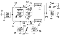
図1は、本発明の実施の形態1に係る周波数逓倍器の回路図である。この周波数逓倍器は入力端子T1に入力された高周波信号の周波数を整数倍して出力端子T2に出力するものである。入力端子T1には入力整合回路10が接続されている。出力端子T2には出力整合回路40が接続されている。
FIG. 1 is a circuit diagram of a frequency multiplier according to
実施の形態1に係る周波数逓倍器は、ソース接地トランジスタである第1トランジスタTr1とゲート接地トランジスタである第2トランジスタTr2を備えている。第1トランジスタTr1は、入力端子T1から高周波信号が入力される第1ゲートG1と、出力端子T2へ出力信号を出す第1ドレインD1と、接地された第1ソースS1とを有する。 The frequency multiplier according to the first embodiment includes a first transistor Tr1 that is a common source transistor and a second transistor Tr2 that is a common gate transistor. The first transistor Tr1 includes a first gate G1 to which a high-frequency signal is input from the input terminal T1, a first drain D1 that outputs an output signal to the output terminal T2, and a grounded first source S1.
第1ゲートG1は、直流遮断用キャパシタ12を介して入力整合回路10に接続されている。第1ゲートG1と接地導体との間には第1ゲートバイアス回路14が接続されている。第1ソースS1と接地導体との間には第1ソースバイアス回路16が接続されている。第1ドレインD1は伝送線路18を介して出力整合回路40に接続されている。
The first gate G1 is connected to the
第2トランジスタTr2は、第2ゲートG2と、入力端子T1から高周波信号が入力される第2ソースS2と、出力端子T2へ出力信号を出す第2ドレインD2とを有する。 The second transistor Tr2 includes a second gate G2, a second source S2 that receives a high frequency signal from the input terminal T1, and a second drain D2 that outputs an output signal to the output terminal T2.
第2ソースS2は、直流遮断用キャパシタ22を介して入力整合回路10に接続されている。第2ソースS2と接地導体の間には第2ソースバイアス回路24が接続されている。第2ゲートG2と接地の間には抵抗である安定化抵抗26とキャパシタ28が接続されている。さらに、第2ゲートG2と接地導体の間には第2ゲートバイアス回路30が接続されている。第2ドレインD2は伝送線路32を介して出力整合回路40に接続されている。
The second source S2 is connected to the
伝送線路18、32の出力側には電源42に接続された電源供給回路44が接続されている。図1から明らかなように、入力端子T1から出力端子T2までの高周波信号の経路上には抵抗がない。
A
本発明の実施の形態1に係る周波数逓倍器の動作について説明する。まず、第1トランジスタTr1のゲートソース間バイアス電圧を第1トランジスタTr1のピンチオフ電圧付近とする。また、第2トランジスタTr2のゲートソース間バイアス電圧を第2トランジスタTr2のピンチオフ電圧付近とする。
The operation of the frequency multiplier according to
そして、入力端子T1に高周波信号(正弦波)を供給すると、第1トランジスタTr1は正の半波を整流したものを出力し、第2トランジスタTr2は負の半波を整流し極性を反転させたものを出力する。第1トランジスタTr1のドレインから出力された信号と第2トランジスタTr2のドレインから出力された信号に含まれる基本波と奇数次高調波は位相が逆相であるので相殺される。第1トランジスタTr1と第2トランジスタTr2のドレインから出力された偶数次高調波は同相であるので強めあう。よって、2倍波周波数電力を出力端子T2から取り出すことができる。 When a high-frequency signal (sine wave) is supplied to the input terminal T1, the first transistor Tr1 outputs a rectified positive half-wave, and the second transistor Tr2 rectifies the negative half-wave and reverses the polarity. Output things. The fundamental wave and the odd harmonics included in the signal output from the drain of the first transistor Tr1 and the signal output from the drain of the second transistor Tr2 are canceled out because the phases are opposite. The even-order harmonics output from the drains of the first transistor Tr1 and the second transistor Tr2 are in-phase and are strengthened. Therefore, the second harmonic frequency power can be taken out from the output terminal T2.
ところで、寄生成分を記述しない簡略化された第1トランジスタTr1のYパラメータ(YSource)は次のように表される。 By the way, the simplified Y parameter (Y Source ) of the first transistor Tr1 not describing the parasitic component is expressed as follows.
![]()
![]()
第2トランジスタTr2のYパラメータ(YGate)は次のように表される。 The Y parameter (Y Gate ) of the second transistor Tr2 is expressed as follows.
![]()
![]()
ここから、出力側の反射係数を表すSパラメータであるS22は次のように表される。この式では安定化抵抗26を考慮していない。
From here, S 22 is an S parameter representing the reflection coefficient of the output side is expressed as follows. This equation does not consider the

この式は、周波数が0及び∞のときに|S22|=1となり、その間の周波数ではすべて1以上であることを示している。実際の素子の特性においては周波数が0及び∞の場合に抵抗成分などにより|S22|<1を示すが、マイクロ波帯やミリ波帯では|S22|>1となり負性抵抗を示す。このように、第2トランジスタ(ゲート接地トランジスタ)を用いた回路では負性抵抗を示す周波数帯域が存在する。その結果、周波数逓倍器全体においても負性抵抗が観測され、特性が不安定となる。 This equation indicates that | S 22 | = 1 when the frequency is 0 and ∞, and all the frequencies in the meantime are 1 or more. In actual device characteristics, when the frequency is 0 and ∞, | S 22 | <1 is indicated by a resistance component or the like, but | S 22 |> 1 in the microwave band or the millimeter wave band, indicating negative resistance. Thus, in a circuit using the second transistor (gate grounded transistor), there is a frequency band indicating a negative resistance. As a result, negative resistance is also observed in the entire frequency multiplier, and the characteristics become unstable.
本発明の実施の形態1の周波数逓倍器は、第2ゲートG2に安定化抵抗26を接続したので、S22は次のように表される。
Frequency multiplier of the first embodiment of the present invention, since the connecting stabilizing
![]()
![]()
安定化抵抗26を設けることで、分母虚数項に2RgmCdgが生じる。したがって、R(安定化抵抗26)を適切に決定することにより|S22|が1を超えないようにすることが可能となる。これによりゲート接地トランジスタである第2トランジスタTr2が負性抵抗を示さなくなり、周波数逓倍器を安定に動作させることが可能となる。
By providing the
このように、安定化抵抗26の抵抗値を、出力側から見たときの反射係数であるS22の絶対値が1を超えない値(1以下)に設定することで、第2トランジスタTr2により生成される反射利得を抑制する。また、高周波信号が通過する経路上に抵抗(ダンピング抵抗)を設けないので、2倍波周波数の電力がダンピング抵抗によって消費され周波数逓倍器の変換利得が低下することを回避できる。
Thus, the resistance value of the stabilizing
本発明の実施の形態1に係る周波数逓倍器は様々な変形をなし得るものである。例えば、ソース接地トランジスタ(第1トランジスタTr1)とゲート接地トランジスタ(第2トランジスタTr2)のゲートソース間バイアス電圧をピンチオフ電圧付近とする手段は特に限定されない。以下の実施の形態に係る周波数逓倍器でも同様である。なお、以下の実施の形態に係る周波数逓倍器は、実施の形態1との共通点が多いので実施の形態1との相違点を中心に説明する。
The frequency multiplier according to
実施の形態2.
図2は、本発明の実施の形態2に係る周波数逓倍器の回路図である。第1ゲートG1に接続された第1ゲートバイアス回路14は抵抗で形成されている。第1ソースS1に接続された第1ソースバイアス回路16は抵抗16aとキャパシタ16bの並列回路で形成されている。このように構成することで、第1トランジスタTr1のゲート電圧及びソース電圧を印加するために個別の電源を必要としない。
FIG. 2 is a circuit diagram of a frequency multiplier according to
第2ソースS2に接続された第2ソースバイアス回路24は抵抗で形成されている。このように構成することで、第2トランジスタTr2のソース電圧を印加するために個別の電源を必要としない。
The second
安定化抵抗26は一端が第2トランジスタTr2のゲートに接続され、他端が接地金属に直接接続されている。この場合、安定化抵抗26がゲートバイアス回路の役割を果たし、ゲート電圧を印加するための個別の電源を必要としない。
One end of the
これにより、第1トランジスタTr1と第2トランジスタTr2のドレイン端子に接続された単一の電源42を用いて、周波数逓倍器を駆動することができる。
As a result, the frequency multiplier can be driven using the
実施の形態3.
図3は、本発明の実施の形態3に係る周波数逓倍器の回路図である。安定化抵抗26の抵抗値Rは、第2トランジスタTr2の負性抵抗を抑制すると同時に、第2トランジスタTr2の利得を減少させる。
Embodiment 3 FIG.
FIG. 3 is a circuit diagram of a frequency multiplier according to Embodiment 3 of the present invention. The resistance value R of the
そこで、安定化抵抗26と並列にキャパシタ50を設けた。つまり、第2ゲートG2と接地との間にキャパシタ50を接続することで、第2トランジスタTr2の利得減少を抑制した。キャパシタ50が入出力整合を変化させ、第2トランジスタTr2の利得減少を抑制する。ただし、キャパシタ50を設けることで安定化の作用(負性抵抗抑制効果)が低下するため、キャパシタ50の容量は小さくする必要がある。
Therefore, a capacitor 50 is provided in parallel with the
実施の形態4.
図4は、本発明の実施の形態4に係る周波数逓倍器の回路図である。高周波信号が通過する主線路から分岐する分岐線路に第1ドレインD1と第2ドレインD2に電位を供給する電源42が設けられている。そして、電源供給回路44として抵抗が設けられている。つまり、分岐線路に直列に抵抗が接続されている。なお、分岐線路と主線路の接続点は接続点P1である。
Embodiment 4 FIG.
FIG. 4 is a circuit diagram of a frequency multiplier according to Embodiment 4 of the present invention. A
マイクロ波又はミリ波帯で用いる素子では、使用周波数に対して1/4波長の線路長の線路と、線路端を高周波で短絡するための容量を用いることが多い。このような線路は、高周波が通る経路に対する接続点から見ると開放端にみえることで、高周波特性への影響をなくしている。 In an element used in a microwave or millimeter wave band, a line having a line length of ¼ wavelength with respect to a used frequency and a capacitor for short-circuiting the line end at a high frequency are often used. Such a line looks like an open end when viewed from a connection point with respect to a path through which a high frequency passes, thereby eliminating the influence on the high frequency characteristics.
接続点P1から見て高周波特性への影響をなくす程度に抵抗値の高い抵抗を電源供給回路として設けると、同時に電圧降下が起きる。よって、増幅器において、電源供給回路を抵抗で形成すると効率が著しく低下する。 When a resistor having a resistance value high enough to eliminate the influence on the high-frequency characteristics when viewed from the connection point P1 is provided as a power supply circuit, a voltage drop occurs simultaneously. Therefore, in the amplifier, when the power supply circuit is formed of a resistor, the efficiency is remarkably lowered.
マイクロ波を周波数逓倍する周波数逓倍器においても、電源供給回路44を抵抗で形成すると、電圧降下は発生する。しかし、周波数逓倍器を流れる電流値は低いため効率低下の影響はシステム全体では小さい。抵抗で形成された電源供給回路44は、1/4波長線路よりも占有面積が非常に小さいので、周波数逓倍器の小型化を図ることが可能である。
Even in the frequency multiplier that multiplies the frequency of the microwave, if the
なお、ここまでで説明した各実施の形態に係る周波数逓倍器の特徴は適宜に組み合わせてもよい。 The features of the frequency multiplier according to each embodiment described so far may be combined as appropriate.
10 入力整合回路、 12 直流遮断用キャパシタ、 14 第1ゲートバイアス回路、 16 第1ソースバイアス回路、 22 直流遮断用キャパシタ、 24 第2ソースバイアス回路、 26 安定化回路、 30 第2ゲートバイアス回路、 40 電源、 42 電源供給回路、 Tr1 第1トランジスタ、 Tr2 第2トランジスタ、 T1 入力端子、 T2 出力端子 10 input matching circuit, 12 DC blocking capacitor, 14 first gate bias circuit, 16 first source bias circuit, 22 DC blocking capacitor, 24 second source bias circuit, 26 stabilization circuit, 30 second gate bias circuit, 40 power supply, 42 power supply circuit, Tr1 first transistor, Tr2 second transistor, T1 input terminal, T2 output terminal
Claims (4)
出力端子と、
前記入力端子から高周波信号が入力される第1ゲートと、前記出力端子へ出力信号を出す第1ドレインと、第1ソースとを有する第1トランジスタと、
第2ゲートと、前記入力端子から前記高周波信号が入力される第2ソースと、前記出力端子へ出力信号を出す第2ドレインと、を有する第2トランジスタと、
一端が前記第2ゲートに接続され、他端が接地導体に直接接続、又はキャパシタを介して接地金属と接続された安定化抵抗と、を備え、
前記入力端子と前記出力端子の間の経路上に抵抗素子がなく、
前記安定化抵抗の抵抗値は、前記安定化抵抗を出力側から見たときの反射係数であるS22の絶対値が1を超えない値に設定したことを特徴とする周波数逓倍器。 An input terminal;
An output terminal;
A first transistor having a first gate that receives a high-frequency signal from the input terminal, a first drain that outputs an output signal to the output terminal, and a first source;
A second transistor having a second gate, a second source to which the high-frequency signal is input from the input terminal, and a second drain for outputting an output signal to the output terminal;
A stabilizing resistor having one end connected to the second gate and the other end connected directly to a ground conductor or connected to a ground metal through a capacitor ;
There is no resistance element on the path between the input terminal and the output terminal ,
The frequency multiplier is characterized in that the resistance value of the stabilization resistor is set to a value in which the absolute value of S22, which is a reflection coefficient when the stabilization resistor is viewed from the output side, does not exceed 1 .
前記第1ソースに接続された第1ソースバイアス回路と、 A first source bias circuit connected to the first source;
前記第2ソースに接続された第2ソースバイアス回路と、を備え、 A second source bias circuit connected to the second source,
前記第1ゲートバイアス回路と、前記第1ソースバイアス回路と、前記第2ソースバイアス回路は、抵抗で形成されたことを特徴とする請求項1に記載の周波数逓倍器。 The frequency multiplier according to claim 1, wherein the first gate bias circuit, the first source bias circuit, and the second source bias circuit are formed of resistors.
前記分岐線路に直列に接続された抵抗と、を備えたことを特徴とする請求項1〜3のいずれか1項に記載の周波数逓倍器。 The frequency multiplier according to claim 1, further comprising a resistor connected in series to the branch line.
Priority Applications (4)
| Application Number | Priority Date | Filing Date | Title |
|---|---|---|---|
| JP2015026705A JP6428341B2 (en) | 2015-02-13 | 2015-02-13 | Frequency multiplier |
| US14/925,344 US9553568B2 (en) | 2015-02-13 | 2015-10-28 | Frequency multiplier |
| DE102016201542.7A DE102016201542B4 (en) | 2015-02-13 | 2016-02-02 | Frequency multiplier |
| CN201610082047.6A CN105897169B (en) | 2015-02-13 | 2016-02-05 | Frequency multiplier |
Applications Claiming Priority (1)
| Application Number | Priority Date | Filing Date | Title |
|---|---|---|---|
| JP2015026705A JP6428341B2 (en) | 2015-02-13 | 2015-02-13 | Frequency multiplier |
Publications (3)
| Publication Number | Publication Date |
|---|---|
| JP2016149708A JP2016149708A (en) | 2016-08-18 |
| JP2016149708A5 JP2016149708A5 (en) | 2017-08-31 |
| JP6428341B2 true JP6428341B2 (en) | 2018-11-28 |
Family
ID=56552510
Family Applications (1)
| Application Number | Title | Priority Date | Filing Date |
|---|---|---|---|
| JP2015026705A Active JP6428341B2 (en) | 2015-02-13 | 2015-02-13 | Frequency multiplier |
Country Status (4)
| Country | Link |
|---|---|
| US (1) | US9553568B2 (en) |
| JP (1) | JP6428341B2 (en) |
| CN (1) | CN105897169B (en) |
| DE (1) | DE102016201542B4 (en) |
Families Citing this family (2)
| Publication number | Priority date | Publication date | Assignee | Title |
|---|---|---|---|---|
| CN107733370B (en) * | 2017-10-12 | 2022-03-04 | 机比特电子设备南京有限公司 | Broadband single-balance frequency tripler based on 0.13um SiGeBiCMOS process |
| CN110112937B (en) * | 2019-04-03 | 2020-11-03 | 东南大学 | Switching transistor rectifier suitable for microwave millimeter wave wireless energy transmission application |
Family Cites Families (13)
| Publication number | Priority date | Publication date | Assignee | Title |
|---|---|---|---|---|
| CA1118849A (en) * | 1979-08-28 | 1982-02-23 | William D. Cornish | Wideband mesfet microwave frequency divider |
| JP2904787B2 (en) | 1988-02-22 | 1999-06-14 | 株式会社日立製作所 | Mixer circuit |
| JP2807508B2 (en) * | 1989-11-15 | 1998-10-08 | 株式会社エイ・ティ・アール光電波通信研究所 | Microwave frequency multiplier |
| JPH0773202B2 (en) | 1989-12-28 | 1995-08-02 | 三菱電機株式会社 | Semiconductor integrated circuit |
| US5661437A (en) * | 1994-08-15 | 1997-08-26 | Nippon Telegraph And Telephone Corporation | Negative feedback variable gain amplifier circuit |
| JPH09153741A (en) * | 1995-09-13 | 1997-06-10 | Fujitsu Ltd | Modulator, indirect modulation type modulator and frequency multiplier |
| JP3970454B2 (en) * | 1998-12-28 | 2007-09-05 | 新日本無線株式会社 | High frequency isolation amplifier |
| JP3366314B2 (en) | 2000-02-29 | 2003-01-14 | 富士通カンタムデバイス株式会社 | Microwave frequency multiplier |
| JP3504598B2 (en) * | 2000-08-18 | 2004-03-08 | 富士通カンタムデバイス株式会社 | Balanced frequency multiplier for microwave or millimeter wave |
| JP2007336048A (en) * | 2006-06-13 | 2007-12-27 | Nec Electronics Corp | High frequency power amplifier |
| JP2010016532A (en) | 2008-07-02 | 2010-01-21 | Japan Radio Co Ltd | Frequency multiplier |
| JP5562671B2 (en) * | 2010-02-05 | 2014-07-30 | 日本無線株式会社 | Frequency multiplier |
| TWI513177B (en) * | 2013-01-02 | 2015-12-11 | Mstar Semiconductor Inc | Frequency multiplier and signal frquency-multiplying method |
-
2015
- 2015-02-13 JP JP2015026705A patent/JP6428341B2/en active Active
- 2015-10-28 US US14/925,344 patent/US9553568B2/en active Active
-
2016
- 2016-02-02 DE DE102016201542.7A patent/DE102016201542B4/en active Active
- 2016-02-05 CN CN201610082047.6A patent/CN105897169B/en not_active Expired - Fee Related
Also Published As
| Publication number | Publication date |
|---|---|
| CN105897169B (en) | 2019-12-10 |
| JP2016149708A (en) | 2016-08-18 |
| US9553568B2 (en) | 2017-01-24 |
| CN105897169A (en) | 2016-08-24 |
| DE102016201542B4 (en) | 2021-10-14 |
| US20160241221A1 (en) | 2016-08-18 |
| DE102016201542A1 (en) | 2016-08-18 |
Similar Documents
| Publication | Publication Date | Title |
|---|---|---|
| JP6632358B2 (en) | Amplifier and voltage regulator | |
| CN111510070A (en) | Resonator circuit | |
| JP5646302B2 (en) | Frequency multiplier | |
| JP6428341B2 (en) | Frequency multiplier | |
| US20110051475A1 (en) | Regulator circuitry for reducing ripple resulted from line voltage transmitting to secondary side of power transformer | |
| JP2009245895A (en) | High-frequency power source | |
| WO2011104802A1 (en) | Frequency multiplier oscillation circuit and method for multiplying fundamental wave | |
| RU2531871C1 (en) | Quartz oscillator | |
| JP2005341447A (en) | High-frequency power amplifier | |
| JP2006261823A (en) | Oscillation circuit | |
| JP6278873B2 (en) | High frequency rectifier | |
| TW201429154A (en) | Frequency multiplier and signal frequency-multiplying method | |
| US9385677B2 (en) | Method and apparatus for gain enhancement of differential amplifier | |
| JP5562671B2 (en) | Frequency multiplier | |
| JP7286031B2 (en) | differential amplifier | |
| JP5773364B2 (en) | EM class amplifier | |
| JP6994884B2 (en) | Oscillator circuit | |
| US20160344341A1 (en) | Electric Circuit Of A Generator Of Oscillations | |
| JP2005223502A (en) | Bias circuit for microwave device | |
| JP5201594B2 (en) | Condenser microphone and its impedance converter | |
| JP2008035302A (en) | Oscillation circuit including output circuit | |
| JP2005204208A (en) | Amplifier | |
| JP2014116889A (en) | Low noise amplifier | |
| JP5854222B2 (en) | Piezoelectric transformer drive device | |
| JP2001024440A (en) | Frequency multiplier |
Legal Events
| Date | Code | Title | Description |
|---|---|---|---|
| A521 | Request for written amendment filed |
Free format text: JAPANESE INTERMEDIATE CODE: A523 Effective date: 20170718 |
|
| A621 | Written request for application examination |
Free format text: JAPANESE INTERMEDIATE CODE: A621 Effective date: 20170718 |
|
| A977 | Report on retrieval |
Free format text: JAPANESE INTERMEDIATE CODE: A971007 Effective date: 20180614 |
|
| A131 | Notification of reasons for refusal |
Free format text: JAPANESE INTERMEDIATE CODE: A131 Effective date: 20180626 |
|
| A521 | Request for written amendment filed |
Free format text: JAPANESE INTERMEDIATE CODE: A523 Effective date: 20180727 |
|
| TRDD | Decision of grant or rejection written | ||
| A01 | Written decision to grant a patent or to grant a registration (utility model) |
Free format text: JAPANESE INTERMEDIATE CODE: A01 Effective date: 20181002 |
|
| A61 | First payment of annual fees (during grant procedure) |
Free format text: JAPANESE INTERMEDIATE CODE: A61 Effective date: 20181015 |
|
| R150 | Certificate of patent or registration of utility model |
Ref document number: 6428341 Country of ref document: JP Free format text: JAPANESE INTERMEDIATE CODE: R150 |
|
| S111 | Request for change of ownership or part of ownership |
Free format text: JAPANESE INTERMEDIATE CODE: R313113 |
|
| R350 | Written notification of registration of transfer |
Free format text: JAPANESE INTERMEDIATE CODE: R350 |
|
| R250 | Receipt of annual fees |
Free format text: JAPANESE INTERMEDIATE CODE: R250 |
|
| R250 | Receipt of annual fees |
Free format text: JAPANESE INTERMEDIATE CODE: R250 |
|
| R250 | Receipt of annual fees |
Free format text: JAPANESE INTERMEDIATE CODE: R250 |