JP6424990B1 - Spacer, surface light source device and image display device - Google Patents
Spacer, surface light source device and image display device Download PDFInfo
- Publication number
- JP6424990B1 JP6424990B1 JP2018536219A JP2018536219A JP6424990B1 JP 6424990 B1 JP6424990 B1 JP 6424990B1 JP 2018536219 A JP2018536219 A JP 2018536219A JP 2018536219 A JP2018536219 A JP 2018536219A JP 6424990 B1 JP6424990 B1 JP 6424990B1
- Authority
- JP
- Japan
- Prior art keywords
- spacer
- optical sheet
- light
- sheet
- light source
- Prior art date
- Legal status (The legal status is an assumption and is not a legal conclusion. Google has not performed a legal analysis and makes no representation as to the accuracy of the status listed.)
- Active
Links
Images


Classifications
-
- F—MECHANICAL ENGINEERING; LIGHTING; HEATING; WEAPONS; BLASTING
- F21—LIGHTING
- F21S—NON-PORTABLE LIGHTING DEVICES; SYSTEMS THEREOF; VEHICLE LIGHTING DEVICES SPECIALLY ADAPTED FOR VEHICLE EXTERIORS
- F21S2/00—Systems of lighting devices, not provided for in main groups F21S4/00 - F21S10/00 or F21S19/00, e.g. of modular construction
-
- G—PHYSICS
- G02—OPTICS
- G02F—OPTICAL DEVICES OR ARRANGEMENTS FOR THE CONTROL OF LIGHT BY MODIFICATION OF THE OPTICAL PROPERTIES OF THE MEDIA OF THE ELEMENTS INVOLVED THEREIN; NON-LINEAR OPTICS; FREQUENCY-CHANGING OF LIGHT; OPTICAL LOGIC ELEMENTS; OPTICAL ANALOGUE/DIGITAL CONVERTERS
- G02F1/00—Devices or arrangements for the control of the intensity, colour, phase, polarisation or direction of light arriving from an independent light source, e.g. switching, gating or modulating; Non-linear optics
- G02F1/01—Devices or arrangements for the control of the intensity, colour, phase, polarisation or direction of light arriving from an independent light source, e.g. switching, gating or modulating; Non-linear optics for the control of the intensity, phase, polarisation or colour
- G02F1/13—Devices or arrangements for the control of the intensity, colour, phase, polarisation or direction of light arriving from an independent light source, e.g. switching, gating or modulating; Non-linear optics for the control of the intensity, phase, polarisation or colour based on liquid crystals, e.g. single liquid crystal display cells
- G02F1/133—Constructional arrangements; Operation of liquid crystal cells; Circuit arrangements
- G02F1/1333—Constructional arrangements; Manufacturing methods
Abstract
本発明の一の態様によれば、第1の光学シート50と、第1の光学シート50と対向するLED実装基板40とを備える面光源装置20に用いられ、かつ第1の光学シート50とLED実装基板40との間に配置され、LED実装基板40に対し第1の光学シート50を離間させる第1のスペーサー60であって、第1の方向DR1に延びる第1の部分63と、第1の方向DR1とは異なる第2の方向DR2に延び、かつ第1の部分63と交差する第2の部分64とを備える壁部62と、壁部62以外の領域に存在し、かつ光を通過させる光通過領域としての開口部61とを備える、第1のスペーサー60が提供される。 According to one aspect of the present invention, it is used for the surface light source device 20 provided with the first optical sheet 50 and the LED mounting substrate 40 facing the first optical sheet 50, and with the first optical sheet 50 A first spacer 60 disposed between the LED mounting substrate 40 and separating the first optical sheet 50 from the LED mounting substrate 40, the first portion 63 extending in the first direction DR1, and A wall 62 having a second portion 64 extending in a second direction DR2 different from the first direction DR1 and intersecting the first portion 63, and exists in a region other than the wall 62, and A first spacer 60 is provided, comprising an opening 61 as a light passage area to be passed.
Description
本願は、先行する日本国出願である特願2016−253328(出願日:2016年12月27日)、特願2016−253332(出願日:2016年12月27日)および特願2017−104442(出願日:2017年5月26日)の優先権の利益を享受するものであり、その開示内容全体は引用することにより本明細書の一部とされる。 The present application is based on Japanese Patent Application No. 2016-253328 (filing date: December 27, 2016), Japanese patent application No. 2016-253332 (filing date: December 27, 2016) and Japanese Patent Application No. 2017-104442, which are prior Japanese applications. Filing date: May 26, 2017), and the entire disclosure of which is incorporated herein by reference.
本発明は、スペーサー、面光源装置および画像表示装置に関する。 The present invention relates to a spacer, a surface light source device, and an image display device.
近年、急速に普及が進んだLED画像表示装置は、通常、液晶表示パネル等の表示画面と、この表示画面を背面側から照明するLED面光源装置とを備えている。現在、LED画像表示装置においては、通常、エッジライト型のLED面光源装置が用いられることが多いが、明るさの観点から、直下型のLED面光源装置を用いることが検討されている。 2. Description of the Related Art An LED image display apparatus, which has been widely spread in recent years, generally comprises a display screen such as a liquid crystal display panel and an LED surface light source apparatus for illuminating the display screen from the back side. Currently, in LED image display devices, edge light type LED surface light source devices are usually used in many cases, but from the viewpoint of brightness, using direct type LED surface light source devices is being studied.
直下型のLED面光源装置においては、LED面光源装置の発光面における輝度の面内均一性を向上させる等の観点から、LED素子上に光学シートを配置している。このような光学シートとして、例えば、LED素子からの光を反射する白色等の樹脂製反射シートに、LED素子直上からLED素子の周囲に向かうに従って徐々に開口部が大きくなるような開口パターンを形成した光透過反射シートを用いる場合がある(特開2010−272245号公報参照)。このような開口パターンを有する光透過反射シートを用いることにより、LED素子直上の光を反射させて周囲に拡散し、周囲の開口部から出光させることができるので、輝度の面内均一性を向上させることができる。 In the direct type LED surface light source device, an optical sheet is disposed on the LED element from the viewpoint of improving the in-plane uniformity of the luminance on the light emitting surface of the LED surface light source device. As such an optical sheet, for example, an opening pattern is formed on a resin reflective sheet such as white that reflects light from the LED element, such that the opening gradually increases from immediately above the LED element toward the periphery of the LED element In some cases, the light transmitting and reflecting sheet may be used (see Japanese Patent Application Laid-Open No. 2010-272245). By using a light transmitting / reflecting sheet having such an opening pattern, light on the LED element can be reflected and diffused to the periphery and emitted from the surrounding openings, thus improving the in-plane uniformity of luminance. It can be done.
光学シートによって、輝度の面内均一性を向上させるためには、LED素子が実装されたLED実装基板に対して、光学シートを離間させる必要がある。このため、通常、LED実装基板と光学シートとの間に、LED実装基板に対して光学シートを離間させるための複数の柱状のスペーサーを配置している。 In order to improve the in-plane brightness uniformity by the optical sheet, it is necessary to separate the optical sheet from the LED mounting substrate on which the LED element is mounted. Therefore, a plurality of columnar spacers are usually disposed between the LED mounting substrate and the optical sheet in order to separate the optical sheet from the LED mounting substrate.
しかしながら、柱状のスペーサーを用いると、スペーサー間で光学シートが撓むおそれがある。特に、光学シートとして光透過反射シートを用いた場合、光透過反射シートに撓みが生じると、LED素子に対する開口パターンの位置が変わるので、輝度の面内均一性が低下してしまうおそれがある。 However, if a columnar spacer is used, the optical sheet may be bent between the spacers. In particular, when a light transmitting / reflecting sheet is used as the optical sheet, if the light transmitting / reflecting sheet is bent, the position of the opening pattern with respect to the LED element is changed, so that the in-plane uniformity of luminance may be reduced.
また、現在、LED画像表示装置を、自動車等の車両や広告媒体に用いることが検討されている。車両においては、車両から振動が発生するので、車両の振動が車両に搭載されたLED画像表示装置にも伝わることがある。さらに、広告媒体においても、例えば、駅のホーム等の看板や車輪等を有する移動式の看板にLED画像表示を用いた場合には、電車等の振動や移動する際の振動がLED画像表示装置にも伝わることがある。 In addition, it is currently considered to use the LED image display device as a vehicle such as a car or an advertisement medium. In a vehicle, vibrations are generated from the vehicle, so the vibrations of the vehicle may be transmitted to the LED image display device mounted on the vehicle. Furthermore, in the case of an advertising medium, for example, when an LED image display is used for a mobile billboard having a signboard such as a station home or the like, a vibration of a train or the like or a vibration when moving is an LED image display device It can also be transmitted.
しかしながら、従来のLED面光源装置においては、振動や衝撃に対する対策が何等採られていないのが現状である。このため、光学シートおよび柱状のスペーサーを備えたLED面光源装置に対し振動試験を行うと、LED素子と光学シートとの位置合わせが正確に行われたとしても、振動によりLED素子に対して光学シートの位置がずれてしまう、いわゆる位置ずれが生じるおそれがある。特に、光学シートとして光透過反射シートを用いた場合、光透過反射シートの位置ずれが生じると、LED素子に対する開口パターンの位置がずれるので、輝度の面内均一性が低下してしまうおそれがある。また、振動試験を行うと、柱状のスペーサーが破損してしまうこともある。 However, in the conventional LED surface light source device, at present, no countermeasure against vibration or impact is taken. Therefore, when a vibration test is performed on the LED surface light source device provided with the optical sheet and the columnar spacer, even if the alignment between the LED element and the optical sheet is accurately performed, the vibration is caused to occur relative to the LED element. There is a possibility that so-called misalignment may occur as the position of the sheet shifts. In particular, when the light transmitting / reflecting sheet is used as the optical sheet, if the light transmitting / reflecting sheet is displaced, the position of the opening pattern with respect to the LED element is displaced, and the in-plane uniformity of luminance may be degraded. . In addition, when the vibration test is performed, the columnar spacer may be broken.
また、光学シートとして光透過反射シートを用いた場合、LED素子が実装されたLED実装基板に対して、光透過反射シートを離間させた状態で、LED素子直上の光を反射させて周囲に拡散し、周囲の開口部から出光させて、輝度の面内均一性の向上を図るので、LED素子と開口パターンとの位置合わせが重要になるが、LED素子に対する位置合わせに関して何等対策が採られていないのが、現状である。 In addition, when a light transmitting / reflecting sheet is used as an optical sheet, light directly on the LED element is reflected and diffused around the LED mounting substrate on which the LED element is mounted, with the light transmitting / reflecting sheet separated. Since the in-plane uniformity of luminance is improved by emitting light from the surrounding opening, the alignment between the LED element and the opening pattern is important, but all measures have been taken for the alignment with respect to the LED element. It is the present condition that there is not.
本発明は、上記問題を解決するためになされたものである。すなわち、光学シートの撓みを抑制でき、振動試験を行った場合であっても、対向部材に対する光学シートの位置ずれを抑制でき、かつ破損しにくいスペーサー、ならびにこれを備えた面光源装置および画像表示装置を提供することを目的とする。また、LED素子に対する第1の光学シートの位置合わせを容易にするとともに、LED素子に対する第1の光学シートの位置ずれを抑制できる面光源装置、およびこれを備えた画像表示装置を提供することを目的とする。 The present invention has been made to solve the above problems. That is, it is possible to suppress the deflection of the optical sheet, and to suppress the displacement of the optical sheet relative to the opposing member even when the vibration test is performed, and a spacer that is not easily damaged, and the surface light source device and image display It aims at providing an apparatus. Further, it is possible to provide a surface light source device capable of facilitating the alignment of the first optical sheet with respect to the LED element and suppressing positional deviation of the first optical sheet with respect to the LED element, and an image display device provided with the same. To aim.
本発明の一の態様によれば、光学シートと、前記光学シートと対向する対向部材とを備える面光源装置に用いられ、かつ前記光学シートと前記対向部材との間に配置され、前記対向部材に対し前記光学シートを離間させるスペーサーであって、第1の方向に延びる第1の部分と、前記第1の方向とは異なる第2の方向に延び、かつ前記第1の部分と交差する第2の部分とを備える壁部と、前記壁部以外の領域に存在し、かつ光を通過させる光通過領域と、を備える、スペーサーが提供される。 According to one aspect of the present invention, it is used in a surface light source device including an optical sheet and an opposing member facing the optical sheet, and disposed between the optical sheet and the opposing member, the opposing member A spacer for separating the optical sheet, wherein a first portion extending in a first direction and a second portion extending in a second direction different from the first direction intersect the first portion; A spacer is provided comprising a wall comprising two parts and a light passing area present in an area other than said wall and passing light.
上記スペーサーにおいて、前記光通過領域が前記スペーサーの高さ方向に貫通する2以上の開口部であり、前記壁部の前記第1の部分および前記第2の部分によって前記開口部間が仕切られていてもよい。 In the spacer, the light passing region is two or more openings penetrating in the height direction of the spacer, and the openings are partitioned by the first portion and the second portion of the wall portion. May be
上記スペーサーにおいて、前記壁部の前記開口部に面している側面が、前記対向部材から前記光学シートに向けて前記開口部の開口径が大きくなるように傾斜していてもよい。 In the spacer, a side surface facing the opening of the wall may be inclined such that an opening diameter of the opening becomes larger from the opposing member toward the optical sheet.
上記スペーサーにおいて、前記壁部のガラス転移温度が、85℃を超えていてもよい。 In the above-mentioned spacer, the glass transition temperature of the above-mentioned wall may be over 85 ° C.
上記スペーサーにおいて、前記壁部の成形収縮率が、1.0%未満であってもよい。 In the spacer, the molding shrinkage of the wall may be less than 1.0%.
上記スペーサーにおいて、前記壁部が、ポリカーボネート樹脂から構成されていてもよい。 In the spacer, the wall portion may be made of polycarbonate resin.
上記スペーサーにおいて、前記壁部が、格子状またはハニカム状であってもよい。 In the spacer, the wall portion may have a lattice shape or a honeycomb shape.
本発明の他の態様によれば、第1の光学シートと、前記第1の光学シートと対向する対向部材と、前記第1の光学シートと前記対向部材との間に配置され、前記対向部材に対し前記第1の光学シートを離間させる第1のスペーサーと、を備え、前記第1のスペーサーが、前記対向部材および前記第1の光学シートと固定されており、前記第1のスペーサーが、上記スペーサーである、面光源装置が提供される。 According to another aspect of the present invention, a first optical sheet, an opposing member facing the first optical sheet, and the opposing member disposed between the first optical sheet and the opposing member And a first spacer for separating the first optical sheet, wherein the first spacer is fixed to the opposing member and the first optical sheet, and the first spacer is A surface light source device, which is the above spacer, is provided.
上記面光源装置において、前記対向部材が、配線基板および前記配線基板の一方の面に実装された複数のLED素子を備えるLED実装基板であり、前記第1の光学シートが、前記LED素子側に配置されていてもよい。 In the surface light source device, the facing member is an LED mounting board including a wiring board and a plurality of LED elements mounted on one surface of the wiring board, and the first optical sheet is on the LED element side It may be arranged.
上記面光源装置において、前記第1の光学シートが、平面視において複数に分割された区画領域を備え、前記各区画領域が、光の一部を透過する複数の透過部と、光の一部を反射する複数の反射部とを有し、前記各区画領域における前記透過部の面積割合である開口率が、前記区画領域の中央部から前記区画領域の外縁部に向けて漸増していてもよい。 In the above-described surface light source device, the first optical sheet includes a plurality of divided regions in plan view, and each of the plurality of divided regions includes a plurality of transmitting portions transmitting a portion of light, and a portion of the light Even if the aperture ratio, which is the area ratio of the transmission part in each of the divided areas, is gradually increased from the center of the divided area toward the outer edge of the divided area. Good.
本発明の他の態様によれば、配線基板、および前記配線基板の一方の面に実装された複数のLED素子を備えるLED実装基板と、前記複数のLED素子と対向するように配置された第1の光学シートと、前記LED実装基板と前記第1の光学シートとの間に配置され、前記配線基板と固定され、前記LED実装基板に対し前記第1の光学シートを離間させる第1のスペーサーと、を備え、前記第1の光学シートが、前記第1のスペーサ側の面に孔部を有し、前記第1のスペーサーが、第1の方向に延びる第1の部分と、前記第1の方向とは異なる第2の方向に延び、かつ前記第1の部分と交差する第2の部分とを備える壁部と、前記壁部以外の領域に存在し、かつ光を通過させる光通過領域と、前記壁部における前記第1の光学シート側の面に設けられ、かつ前記孔部に入り込んだ1以上の凸部と、を備えていてもよい。 According to another aspect of the present invention, there is provided an LED mounting board including a wiring board and a plurality of LED elements mounted on one surface of the wiring board, and a plurality of LED mounting boards arranged to face the plurality of LED elements. A first spacer which is disposed between the first optical sheet, the LED mounting board, and the first optical sheet, is fixed to the wiring board, and separates the first optical sheet from the LED mounting board And the first optical sheet has a hole in a surface on the first spacer side, and the first spacer has a first portion extending in a first direction; And a light passing area that is present in a region other than the wall and that allows light to pass through, and a wall including a second portion that extends in a second direction different from the direction of the second direction and that intersects the first portion And at the side of the first optical sheet in the wall portion Provided, and 1 and more convex portions entering into the hole portion may be provided with a.
上記面光源装置において、前記光通過領域が前記第1のスペーサーの高さ方向に貫通する2以上の開口部であり、前記壁部の前記第1の部分および前記第2の部分によって前記開口部間が仕切られていてもよい。 In the surface light source device, the light passing area is two or more openings penetrating in the height direction of the first spacer, and the opening is formed by the first portion and the second portion of the wall portion. A space may be divided.
上記面光源装置において、前記第1の光学シートが、平面視において複数に分割された区画領域を備え、前記各区画領域が、光の一部を透過する複数の透過部と、光の一部を反射する複数の反射部とを有し、前記各区画領域における前記透過部の面積割合である開口率が、前記区画領域の中央部から前記区画領域の外縁部に向けて漸増していてもよい。 In the above-described surface light source device, the first optical sheet includes a plurality of divided regions in plan view, and each of the plurality of divided regions includes a plurality of transmitting portions transmitting a portion of light, and a portion of the light Even if the aperture ratio, which is the area ratio of the transmission part in each of the divided areas, is gradually increased from the center of the divided area toward the outer edge of the divided area. Good.
上記面光源装置において、前記第1の光学シートの前記透過部が、前記第1の光学シートの厚さ方向に貫通する開口部であり、前記開口部の少なくとも1つが、前記孔部として機能してもよい。 In the above-described surface light source device, the transmission portion of the first optical sheet is an opening penetrating in the thickness direction of the first optical sheet, and at least one of the openings functions as the hole. May be
上記面光源装置において、前記第1の光学シートの厚みが、25μm以上1mm以下であってもよい。 In the surface light source device, the thickness of the first optical sheet may be 25 μm or more and 1 mm or less.
上記面光源装置において、前記配線基板が、可撓性を有する樹脂フィルムと、前記樹脂フィルムより前記第1の光学シート側に設けられ、かつ前記LED素子と電気的に接続された金属配線部とを備えるフレキシブル配線基板であってもよい。 In the above-described surface light source device, the wiring substrate is a resin film having flexibility, and a metal wiring portion provided on the first optical sheet side with respect to the resin film and electrically connected to the LED element. It may be a flexible wiring board provided with
上記面光源装置において、前記第1の光学シートの光出射側に配置された第2の光学シートと、前記第1の光学シートの外周面および前記第1のスペーサーの外周面を取り囲むように配置され、かつ前記第1の光学シートに対し前記第2の光学シートを離間させる枠状の第2のスペーサーとをさらに備えていてもよい。 In the surface light source device, the second optical sheet disposed on the light emitting side of the first optical sheet, the outer peripheral surface of the first optical sheet, and the outer peripheral surface of the first spacer are disposed so as to surround them. And a frame-shaped second spacer for separating the second optical sheet from the first optical sheet.
本発明の他の態様によれば、上記面光源装置と、前記面光源装置よりも観察者側に配置された表示パネルとを備える、画像表示装置が提供される。 According to another aspect of the present invention, there is provided an image display device comprising the surface light source device and a display panel disposed closer to the viewer than the surface light source device.
本発明の一の態様によれば、光学シートの撓みを抑制でき、振動試験を行った場合であっても、対向部材に対する光学シートの位置ずれを抑制でき、かつ破損しにくいスペーサーを提供することができる。また、本発明の他の態様によれば、このようなスペーサーを備える面光源装置および画像表示装置を提供することができる。また、本発明の他の態様によれば、LED素子に対する第1の光学シートの位置合わせを容易にするとともに、LED素子に対する第1の光学シートの位置ずれを抑制できる面光源装置、およびこれを備えた画像表示装置を提供することができる。 According to one aspect of the present invention, it is possible to suppress deflection of the optical sheet, and to provide a spacer that can suppress positional deviation of the optical sheet with respect to the opposing member even when a vibration test is performed, and is not easily damaged. Can. Moreover, according to the other aspect of this invention, the surface light source device provided with such a spacer and an image display apparatus can be provided. Further, according to another aspect of the present invention, a surface light source device capable of facilitating the alignment of the first optical sheet with respect to the LED element and suppressing the displacement of the first optical sheet with respect to the LED element, and An image display device provided can be provided.
[第1の実施形態]
以下、本発明の第1の実施形態に係るスペーサー、直下型の面光源装置および画像表示装置について、図面を参照しながら説明する。本明細書において、「LED」とは、発光ダイオードを意味するものである。また、「シート」、「フィルム」、「板」等の用語は、呼称の違いのみに基づいて、互いから区別されるものではない。したがって、例えば、「シート」は、フィルムや板とも呼ばれるような部材も含む意味で用いられる。図1は本実施形態に係る画像表示装置の分解斜視図であり、図2は本実施形態に係る画像表示装置の概略構成図であり、図3は本実施形態に係る面光源装置の一部の拡大断面図である。図4は図1に示される第1の光学シートの平面図であり、図5は図1に示される第1のスペーサーの平面図であり、図6は図1に示される第1の光学シートと第1のスペーサーとの配置関係を示す平面図である。図7〜図12は本実施形態に係る他の第1のスペーサーの平面図であり、図13および図14は本実施形態に係る他の仕切部の一部の断面図であり、図15は第1のスペーサーの第1の部分と第2の部分の交差部の斜視図であり、図16は図1に示される第1のスペーサーと第2のスペーサーとの配置関係を示す平面図であり、図17は図1に示されるレンズシートの断面図である。First Embodiment
Hereinafter, a spacer, a direct-type surface light source device, and an image display device according to a first embodiment of the present invention will be described with reference to the drawings. In the present specification, "LED" means a light emitting diode. Also, terms such as "sheet", "film", "plate" and the like are not distinguished from one another based only on the difference in designation. Thus, for example, "sheet" is used to include members such as a film or a plate. FIG. 1 is an exploded perspective view of the image display apparatus according to the present embodiment, FIG. 2 is a schematic configuration view of the image display apparatus according to the present embodiment, and FIG. 3 is a part of the surface light source apparatus according to the present embodiment. FIG. 4 is a plan view of the first optical sheet shown in FIG. 1, FIG. 5 is a plan view of the first spacer shown in FIG. 1, and FIG. 6 is the first optical sheet shown in FIG. It is a top view which shows the arrangement | positioning relationship of and the 1st spacer. FIGS. 7 to 12 are plan views of other first spacers according to the present embodiment, and FIGS. 13 and 14 are cross-sectional views of part of other partitions according to the present embodiment, and FIG. FIG. 16 is a perspective view of the intersection of the first portion and the second portion of the first spacer, and FIG. 16 is a plan view showing the positional relationship between the first spacer and the second spacer shown in FIG. FIG. 17 is a cross-sectional view of the lens sheet shown in FIG.
<<<<画像表示装置>>>>
図1および図2に示される画像表示装置10は、直下型の面光源装置20と、面光源装置20よりも観察者側に配置された表示パネル120とを備えている。<<<< image display device >>>>
The
<<<表示パネル>>>
図1および図2に示される表示パネル120は、液晶表示パネルであり、入光側に配置された偏光板121と、出光側に配置された偏光板122と、偏光板121と偏光板122との間に配置された液晶セル123とを備えている。偏光板121、122および液晶セル123としては、公知の偏光板および液晶セルを用いることができる。<<< Display panel >>>
The
<<<面光源装置>>>
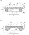
図1または図2に示される面光源装置20は、筐体30と、LED実装基板40と、第1の光学シート50と、第1のスペーサー60と、第2の光学シート70と、第2のスペーサー80とを備えている。また、面光源装置20は、その他、第2の光学シート70に積層されたレンズシート90および反射型偏光分離シート100を備えている。なお、面光源装置20は、LED実装基板40、第1の光学シート50、および第1のスペーサー60を備えていればよく、筐体30、第2の光学シート70、第2のスペーサー80、レンズシート90、または反射型偏光分離シート100を備えていなくともよい。第1のスペーサー60は、光学シートと、光学シートと対向する対向部材とを備える面光源装置に用いられるものである。面光源装置20においては、光学シートが第1の光学シート50であり、対向部材がLED実装基板40となっている。なお、対向部材は、光学シートと対向する部材であれば、LED実装基板でなくともよい。<<< Area light source device >>>
The surface
車載用面光源装置は車両内の非常に狭い空間に配置されるので、一般の面光源装置よりも薄型化を図ることが望まれている。このため、面光源装置20の総厚は、薄型化を図る観点から、15mm以下となっていることが好ましく、10mm以下となっていることがより好ましい。「面光源装置」の総厚とは、図2に示される筐体30の外底面30Cから反射型偏光分離シート100の表面100Aまでの距離を意味するものとする。
Since the in-vehicle surface light source device is disposed in a very narrow space in the vehicle, it is desired to make it thinner than a general surface light source device. For this reason, the total thickness of the surface
<<筐体>>
筐体30は、LED実装基板40等を収容する収容空間30Aを備えている。筐体30は、図2または図3に示されるように、内側の底面である内底面30B、外側の底面である外底面30C、および内底面30Bから立ち上がる内側の側面である内側面30Dを有している。また、筐体30は、図2に示されるように、LED素子42からの光を筐体30から出射させるための開口部30Eを有している。開口部30Eは、内底面30Bに対向する位置に設けられていることが好ましい。開口部30Eの形状は、特に限定されず、例えば、矩形状または円形状が挙げられる。<< case >>
The
図2に示される筐体30は、収容空間30Aを有する筐体本体31と、筐体本体31の収容空間30Aを覆い、かつ開口部30Eを有する枠状の蓋体32とを備えている。筐体30においては、筐体30の内底面30Bは筐体本体31の内底面となっており、筐体30の内側面30Dは筐体本体31の内側面となっている。
The
筐体30(筐体本体31および蓋体32)は、金属から構成されていることが好ましい。特に、筐体本体31を金属から構成することによって、筐体本体31が放熱構造体としても機能するので、LED素子42からの熱を効率良く、放熱させることができる。金属としては、特に限定されないが、例えば、アルミニウム等が挙げられる。
The housing 30 (the
<<LED実装基板>>
LED実装基板40は、第1の光学シート50に対向するように配置されている。LED実装基板40は、配線基板41と、配線基板41の一方の面(以下、この面を「表面」と称する。)41Aに実装された複数のLED素子42とを備えている。LED実装基板40は、図2および図3に示されるように、配線基板41におけるLED素子42が実装された表面41Aとは反対側の面(以下、この面を「裏面」と称する)41Bが筐体30の内底面30B側に位置するように筐体30内に配置されている。<< LED mounting board >>
The
<配線基板>
配線基板41は、筐体30の内底面30Bに沿って配置されている。配線基板41の裏面41Bは、筐体30の内底面30Bと接していることが好ましい。配線基板41における裏面41Bが筐体30の内底面30Bと接することにより、配線基板41等の熱を効率良く筐体30側に放熱させることができる。本明細書において、「配線基板の裏面が筐体の内底面と接している」とは、配線基板の裏面が筐体の内底面に直接接触している場合に限らず、配線基板の裏面と筐体の内底面との間に、両面テープ、粘着剤または接着剤等、熱伝導という観点でほぼ無視できる層が介在している場合をも含む概念である。<Wiring board>
The
配線基板41においては、図3に示されるように、第1の光学シート50に向けて、樹脂フィルム43と、金属配線部44と、絶縁性保護膜45と、反射層46とがこの順で積層されている。ただし、配線基板41は、絶縁性保護膜45や反射層46を備えていなくともよい。また、金属配線部44は、樹脂フィルム43に対し、接着層47を介したドライラミネート法によって接着されていることが好ましい。さらに、金属配線部44は、LED素子42と半田層48を介して電気的に接続されている。
In the
配線基板41は、リジット配線基板であってもよいが、フレキシブル配線基板であることが好ましい。配線基板41が、フレキシブル配線基板であることにより、曲げ可能な面光源装置を得ることも可能になる。図2に示される配線基板41は、フレキシブル配線基板である。「フレキシブル」とは、柔軟性があることを意味しており、「フレキシブル配線基板」とは、一般的に可撓性があり、曲げることが可能な配線基板を意味するものとする。本明細書における「可撓性」とは、少なくとも曲率半径が1mとなるように曲がることを意味する。フレキシブル配線基板は、曲率半径が、好ましくは50cm、より好ましくは30cm、更に好ましくは10cm、特に好ましくは5cmとなるように曲がる。
The
(樹脂フィルム)
樹脂フィルム43は、可撓性を有している。樹脂フィルム43は、曲率半径が、好ましくは50cm、より好ましくは30cm、更に好ましくは10cm、特に好ましくは5cmとなるように曲がるフィルムである。(Resin film)
The
樹脂フィルム43は、公知の熱可塑性樹脂を用いて形成することができる。樹脂フィルム43の材料として用いる熱可塑性樹脂には耐熱性および絶縁性が高いものであるが好ましい。このような樹脂として、耐熱性と加熱時の寸法安定性、機械的強度、および耐久性に優れるポリイミド(PI)や、ポリエチレンナフタレート(PEN)を用いることができる。これらの中でも、アニール処理等の耐熱性向上処理を施すことによって耐熱性と寸法安定性を向上させたポリエチレンナフタレート(PEN)を好ましく用いることもできる。また、難燃性の無機フィラー等の添加によって難燃性を向上させたポリエチレンテレフタレート(PET)も樹脂フィルムを形成するための樹脂として選択することができる。
The
樹脂フィルム43を形成する熱可塑性樹脂は、熱収縮開始温度が100℃以上のもの、または、上記のアニール処理等によって、同温度が100℃以上となるように耐熱性を向上させたものを用いることが好ましい。本明細書における「熱収縮開始温度」とは、熱機械分析(TMA)装置に測定対象の熱可塑性樹脂からなるサンプルフィルムをセットし、荷重1gを加えて、昇温速度2℃/分で120℃まで昇温し、その時の収縮量(%)を測定し、このデータを出力して温度と収縮量を記録したグラフから、収縮によって、0%のベースラインから離れる温度を読みとり、その温度を熱収縮開始温度としたものである。なお、熱収縮開始温度は、3回測定して得られた値の算術平均値とする。
As the thermoplastic resin for forming the
通常LED素子からの熱によりLED素子周辺部は90℃程度の温度に達する場合がある。この観点から、樹脂フィルム43を形成する熱可塑性樹脂は、上記温度以上の耐熱性を有するものであることが好ましい。
In general, the temperature around the LED element may reach a temperature of about 90 ° C. due to the heat from the LED element. From this viewpoint, it is preferable that the thermoplastic resin forming the
樹脂フィルム43には、配線基板41に必要な絶縁性を付与し得るだけの高い絶縁性を有する樹脂であることが求められる。このため、樹脂フィルム43は、その体積固有抵抗率が1014Ω・cm以上であることが好ましく、1018Ω・cm以上であることがより好ましい。体積固有抵抗率は、JIS C2151:2006に準拠した方法で測定することができる。体積固有抵抗率は、ランダムに10箇所測定し、測定した10箇所の体積固有抵抗率の算術平均値とする。The
樹脂フィルム43の厚みは、特に限定されないが、放熱経路としてボトルネックとはならないこと、耐熱性および絶縁性を有するものであること、ならびに、製造コストのバランスとの観点から、概ね10μm以上500μm以下であることが好ましい。また、ロール・トゥ・ロール方式による製造を行う場合の生産性を良好に維持する観点からも上記厚み範囲であることが好ましい。樹脂フィルム43の厚みは、走査型電子顕微鏡(SEM)を用いて、樹脂フィルム43の断面を撮影し、その断面の画像において樹脂フィルム43の任意の10箇所の厚みを測定し、その平均値を算出することにより求めるものとする。樹脂フィルム43の厚みの下限は、15μm以上であることが好ましく、50μm以上であることがより好ましく、樹脂フィルム43の厚みの上限は、250μm以下であることが好ましい。
The thickness of the
(金属配線部)
金属配線部44は、樹脂フィルム43よりLED素子42側に設けられ、かつLED素子42と電気的に接続されている。金属配線部44は、金属箔等をパターニングすることによって形成することができる。(Metal wiring section)
The
金属配線部44を構成する金属の熱伝導率λは200W/(m・K)以上500W/(m・K)以下が好ましい。熱伝導率λは、例えば、熱伝導率計(製品名「QTM−500」、京都電子工業株式会社製)を用いて測定することができる。熱伝導率λは、3回測定して得られた値の算術平均値とする。上記熱伝導率の下限は、300W/(m・K)以上であることがより好ましく、上限は500W/(m・K)以下であることが好ましい。銅の場合、熱伝導率λは403W/(m・K)である。
The thermal conductivity λ of the metal constituting the
金属配線部44を構成する金属の電気抵抗率Rは3.00×10⁻⁸Ωm以下が好ましく、2.50×10⁻⁸Ωm以下がより好ましい。電気抵抗率Rは、エレクトロメータ(製品名「6517B型エレクトロメータ」、ケースレー社製)を用いて測定することができる。電気抵抗率Rは、3回測定して得られた値の算術平均値とする。銅の場合、電気抵抗率Rは1.55×10⁻⁸Ωmとなる。3.00 * 10 < -8 > (ohm) m or less is preferable, and, as for the electrical resistivity R of the metal which comprises the
例えば、金属配線部44を銅箔で形成した場合、放熱性と電気伝導性を高い水準で両立させることができる。より具体的には、LED素子からの放熱性が安定し、電気抵抗の増加を防げるので、LED間の発光バラツキが小さくなってLEDの安定した発光が可能となる。また、LED素子の寿命も延長される。更に、熱による樹脂フィルム等の周辺部材の劣化も防止できるので、面光源装置を組み込んだ画像表示装置の製品寿命も延長できる。
For example, when the
金属配線部44を形成する金属の例としては、上記の銅の他、アルミニウム、金、銀等の金属を挙げることができる。
As an example of the metal which forms the
金属配線部44は電解銅箔であり、また、金属配線部44における樹脂フィルム43側の面の十点平均粗さRzが1.0μm以上10.0μm以下であることがより好ましい。十点平均粗さRzを上記範囲内とすることで、特に金属配線部44における樹脂フィルム43側の面の表面積を増大させることができ、放熱性を更に高めることができる。また、この面が凹凸面となっているので、樹脂フィルム43との密着性をより向上でき、これによっても放熱性を向上できる。このような十点平均粗さRzを有する電解銅箔の面としては、電解銅箔の粗面側(マット面側)を好適に用いることができる。十点平均粗さRzは、JIS B0601:1999に準拠して、例えば、表面粗さ測定器(製品名「SE−3400」、株式会社小坂研究所製)を用いて測定することができる。十点平均粗さRzは、3回測定して得られた値の算術平均値とする。
The
金属配線部44の配置は、LED素子42の導通可能な配置、好ましくはLED素子42をマトリックス状に配置できるものであれば、特定の配置に限定されない。ただし、配線基板41においては、樹脂フィルム43の一方の表面の好ましくは80%以上、より好ましくは90%、最も好ましくは95%以上の範囲が、この金属配線部44によって被覆されていることが好ましい。これにより、LED素子42を高密度で配置することができるとともに、発生する過剰な熱を、十分に金属配線部44を通じて速やかに拡散させ、樹脂フィルム43を経由させて外部へ放熱させることができるので、優れた放熱性を有する面光源装置20を得ることができる。
The arrangement of the
金属配線部44の厚みは、配線基板41に要求される耐電流の大きさ等に応じて適宜設定すればよく、特に限定されないが、一例として10μm以上50μm以下としてもよい。放熱性向上の観点から、金属配線部44の厚みは、10μm以上であることが好ましい。また、金属配線部の厚さが10μm未満であると、樹脂フィルム43の熱収縮の影響が大きく、半田リフロー処理時に処理後の反りが大きくなりやすいため、この観点からも金属配線部44の厚さは10μm以上であることが好ましい。一方、金属配線部の厚さが、50μm以下であることによって、配線基板の十分なフレキシブル性を維持することができ、重量増大によるハンドリング性の低下等も防止できる。金属配線部44の厚さは、樹脂フィルム43と同様の方法によって測定することができる。
The thickness of the
(絶縁性保護膜)
絶縁性保護膜45は、主として配線基板41の耐マイグレーション特性を向上させるものである。絶縁性保護膜45は、金属配線部44の表面のうちLED素子42を実装するための接続部分を除く全面、および樹脂フィルム43の表面のうち金属配線部44の非形成部分の概ね全面を覆う態様で形成されている。(Insulating protective film)
The insulating
絶縁性保護膜45は、熱硬化性樹脂を含む熱硬化性樹脂組成物の硬化物から構成されていることが好ましい。熱硬化性樹脂組成物としては、熱硬化温度が100℃以下程度のものであれば、公知の熱硬化性樹脂組成物を適宜好ましく用いることができる。具体的には、ポリエステル系樹脂、エポキシ系樹脂、エポキシ系およびフェノール系樹脂、エポキシアクリレート樹脂、シリコーン系樹脂等をそれぞれベース樹脂とする熱硬化性樹脂組成物を好ましく用いることができる。また、これらのうちでも、ポリエステル系樹脂を含む熱硬化性樹脂組成物は、可撓性に優れる点から、絶縁性保護膜45を形成するための材料として特に好ましい。
The insulating
絶縁性保護膜45を形成するための熱硬化性樹脂組成物は、例えば、二酸化チタン等の無機白色顔料を更に含有する白色の熱硬化性樹脂組成物であってもよい。絶縁性保護膜45を白色化することで、意匠性の向上を図ることができる。また、反射層の機能を絶縁性保護膜45に付与することもできる。
The thermosetting resin composition for forming the insulating
絶縁性の熱硬化性樹脂組成物を用いた絶縁性保護膜45の形成は、スクリーン印刷等の公知の方法によって行うことができる。
The formation of the insulating
絶縁性保護膜45の膜厚は、10μm以上100μm以下であることが好ましい。絶縁性保護膜45の膜厚が、10μm未満であると、絶縁性が低下するおそれがあり、また100μmを超えると、絶縁性保護層をスクリーン印刷によって形成する際の滲みや熱硬化時の収縮による配線基板の反り等が顕著に生じるおそれがある。絶縁性保護膜45の膜厚は、走査型電子顕微鏡(SEM)を用いて、絶縁性保護膜45の断面を撮影し、その断面の画像において絶縁性保護膜45の膜厚を20箇所測定し、その20箇所の膜厚の算術平均値とする。
The film thickness of the insulating
(反射層)
反射層46は、主として波長380nm以上780nm以下の可視光波長域の光に対して高い反射性を有するものである。反射層46は、面光源装置20の発光能力の向上を目的として、配線基板41の表面41Aに、LED素子実装領域を除く領域を覆って積層されている。なお、この実施形態においては、反射層46は、平面視において、LED素子42を囲い、かつ、絶縁性保護膜45のLED素子実装領域によって除かれた領域の内周縁部が露出するように絶縁性保護膜45上に積層されている。また、これに限らず、例えば、絶縁性保護膜45のLED素子実装領域によって除かれた領域の内周縁部が露出せず、絶縁性保護膜45と反射層46との両方の内周縁部が一致して同一形状をなすように積層されていてもよい。(Reflective layer)
The
反射層46は、LED素子42からの光を反射し、所定の方向へ導くための反射面を持つ部材であれば、特に限定されないが、発泡タイプの白色ポリエステル、白色ポリエチレン樹脂、銀蒸着ポリエステル等を、最終製品の用途とその要求スペック等に応じて適宜用いることができる。
The
反射層46の膜厚は、50μm以上1mm以下であることが好ましい。反射層46の膜厚が、50μm未満であると、所望の反射率が得られないおそれがあり、また反射層が薄すぎるので、所定の位置にセッティングしにくくなり、また1mmを超えると、高コストとなるとともに、面光源装置の薄型化を達成できないおそれがある。反射層46の膜厚は、絶縁性保護膜45の膜厚と同様の方法によって測定することができる。
The film thickness of the
(接着層)
接着層47としては、公知の樹脂系接着剤を適宜用いることができる。それらの樹脂系接着剤のうち、ウレタン系、ポリカーボネート系、又はエポキシ系の接着剤等を特に好ましく用いることができる。この接着層47は、金属配線部44のエッチング処理後に樹脂フィルム43上に残存している。(Adhesive layer)
As the
(半田層)
半田層48は、金属配線部44とLED素子42とを電気的および機械的に接合するためものである。この半田層48による接合方法としては、大きく分けて、リフロー方式あるいはレーザー方式があるが、このいずれかによって行うことができる。(Solder layer)
The
金属配線部とLED素子とを半田によって接合する際、樹脂フィルムおよび金属配線部には多大な熱が加えられるので、樹脂フィルムと金属配線部の線膨張係数の違いから、樹脂フィルムおよび金属配線部を備える配線基板に反りが発生するおそれがある。このような反りを防ぐために、樹脂フィルム43における金属配線部44側の面とは反対側の面に金属箔を設けることが好ましい。また、このような金属箔を設けることにより、点灯時のLED実装基板40の熱をより筐体本体31に放熱させることもできる。
When the metal wiring portion and the LED element are joined by solder, a large amount of heat is applied to the resin film and the metal wiring portion, and therefore, the resin film and the metal wiring portion are different from each other There is a possibility that warpage may occur in the wiring substrate provided with In order to prevent such warpage, it is preferable to provide a metal foil on the surface of the
<<LED素子>>
LED素子42は、P型半導体とN型半導体が接合されたPN接合部での発光を利用した発光素子である。LED素子としては、P型電極、N型電極を素子上面、下面に設けた構造と、素子片面にP型、N型電極の双方が設けられた構造が知られているが、いずれの構造のLED素子も、面光源装置20に用いることができる。ただし、上記のうち素子片面にP型、N型電極の双方が設けられた構造のLED素子を特に好ましく用いることができる。<< LED device >>
The
LED素子42は、配線基板41上にマトリクス状に配置されている。本明細書における「マトリクス状」とは、行列状に二次元配列されている状態を意味するものとする。本実施形態においては、LED素子42はマトリクス状に配置されているが、LED素子の配置状態は、特に限定されず、例えば、LED素子は千鳥状に配置されていてもよい。LED素子42は配線基板41上に複数個実装されている。配線基板41に実装されるLED素子42の個数は、複数個であれば、特に限定されない。LED素子42の配置密度は、0.02個/cm2以上2.0個/cm2以下であることが好ましく、0.1個/cm2以上1.5個/cm2以下であることがより好ましい。The
<<第1の光学シート>>
第1の光学シート50は、光学的な機能を有するシートである。第1の光学シートとしては、例えば、光透過反射シート等が挙げられる。図1および図2に示される第1の光学シート50は、光透過反射シートとなっている。光透過反射シートは、光を透過させる透過部と光を反射させる反射部を有し、ある部分では光を透過させ、他の部分では光を反射させることで、LED素子からの光を平面内に拡散させて、輝度の面内均一性を向上させる機能を有するものである。<< First Optical Sheet >>
The first
第1の光学シート50は、LED実装基板40における複数のLED素子42と対向するように配置されている、また、第1の光学シート50は、第1のスペーサー60によってLED実装基板40に対して離間している。第1の光学シート50は、配線基板41と略平行に配置されている。
The first
図3に示される配線基板41の表面41Aから第1の光学シート50までの距離d1は0.6mm以上6mm以下となっている。本明細書における「配線基板の表面から第1の光学シートまでの距離」とは、配線基板41のように絶縁性保護層上に反射層を備えており、反射層の表面が配線基板の表面となっている場合には、反射層の表面から第1の光学シートにおける配線基板側の面までの距離を意味し、また配線基板の絶縁性保護層が反射層の機能を兼ね備えており、絶縁性保護層の表面が配線基板の表面となっている場合には、絶縁性保護層の表面から第1の光学シートにおける配線基板側の面までの距離を意味するものとする。また、第1の光学シートにおける配線基板側の面とは、第1の光学シートにおける配線基板側の面が樹脂フィルムの面のみから構成されている場合には、樹脂フィルムにおける配線基板側の面であるが、第1の光学シート50のように、樹脂フィルム54よりも配線基板41側に反射層55が形成されている場合には、反射層55における配線基板41側の面とする。
The distance d1 from the
第1の光学シート50の厚みは、25μm以上1mm以下であることが好ましい。光透過反射シートの厚みが、25μm未満であると、所望の反射率が得られないおそれがあり、また1mmを超えると、面光源装置の薄型化が図れないおそれがある。第1の光学シート50の厚みは、後述する反射部53の厚みとし、走査型電子顕微鏡(SEM)を用いて、第1の光学シート50の断面を撮影し、その断面の画像において第1の光学シート50の任意の10箇所の厚さを測定し、その平均値を算出することにより求めることができる。第1の光学シート50は、図4に示されるように、平面視において複数に分割された区画領域51を備えている。
The thickness of the first
<区画領域>
区画領域51は、LED素子42の個数に合わせて分割されていることが好ましい。図4においては、LED素子(縦4個×横6個=24個)に対応して、縦4個×横6個=24個の区画領域51が形成されている。なお、図4においては点線で境界線が記載されているが、実際には境界線が形成されていることはなく、境界線は仮想線であり、区画領域51も仮想の領域である。<Division area>
It is preferable that the
各区画領域51は、図4に示されるようにLED素子42からの光の一部を透過する複数の透過部52と、LED素子42からの光の一部を反射する複数の反射部53とで構成されている。透過部52および反射部53は、所定のパターンで構成されている。各区画領域におけるLED素子に対応する部分は最も多くの光が入射する部分となるので、この部分から光が透過すると、この部分の輝度が区画領域の他の部分の輝度よりも高くなってしまい、輝度の面内均一性が低下するおそれがある。このため、各区画領域51におけるLED素子42に対応する部分は反射部53から構成されていることが好ましい。なお、図4においては、形式的に、透過部52を白色で表しており、反射部53を灰色で表している。また、各区画領域51における透過部52および反射部53のパターンは同じとなっているが、必ずしも同じである必要はなく、区画領域によって異なるパターンであってもよい。透過部52および反射部53は、マス目状のパターンであってもよい。
As shown in FIG. 4, each divided
第1の光学シート50は、図4に示されるように、各区画領域51の中央部51Aが各LED素子42と対応する領域となるように配置されているので、外縁部51Bよりも中央部51Aに入射する光量は多くなる。このため、各区画領域51においては、透過部52の面積割合である開口率は、中央部51Aから外縁部51Bに向けて漸増していることが好ましい。各区画領域51における開口率を、中央部51Aから外縁部51Bに向けて漸増させることにより、十分な光量を確保した上で、発光面上における輝度の均一性をより向上させることができる。本明細書における区画領域の「開口率」とは、一の区画領域を、25〜100等分程度の適当な割合で当分する等面積の正方形のマス目状に区切った際に、それぞれのマス目における透過部の面積比率のことを意味する。一の区画領域におけるこの等面積のマス目の規定の仕方は任意であるが、例えば、各マス目内に存在する透過部の個数が概ね等数となるように設定することが望ましい。また、「開口率」は、一の区画領域の中心点を中心とする同心円を中央領域から中央領域の外側に位置する外側領域に向けて等間隔で複数規定し、各同心円の円周と円周の間の各領域内における透過部の面積比率を上記同様にして算出することによって求めたものであってもよい。この算出方法によれば、矩形の開口部が格子状に配置された一般的な開口配置以外の区画領域についても、上記の「開口率」を定義することができる。なお、各区画領域51においては、開口率が中央部51Aから外縁部51Bに向けて漸増していればよく、例えば中央部や外縁部近傍の限定された一部範囲において開口率が一定である領域が存在していてもよい。
Since the first
各区画領域51の中央部51Aにおいては、面積比が反射部>透過部となっていることが好ましく、輝度の面内均一性を向上させる観点から、各区画領域51の中央部51Aは、反射部53のみから構成することがより好ましい。また、各区画領域51の外縁部51Bにおいては、面積比が透過部>反射部となっていることが好ましい。具体的には、外縁部51Bにおける透過部52の面積割合は、50%以上100%以下であることが好ましい。外縁部51Bにおける透過部52の面積割合の下限は、60%以上であることがより好ましく、70%以上であることがさらに好ましい。なお、外縁部51Bでは反射部53を島状に形成することによって、理論的には透過部の面積割合を100%にすることもできる。このことは、従来の打ち抜き開口方式の光透過反射シートではなし得ない構成である。このように、第1の光学シート50の透過部52および反射部53を印刷方法によりパターン形成する場合には、パターニングのフレキシビリティを拡大させることができる。
In the
第1の光学シート50は、図3に示されるように、樹脂フィルム54と、樹脂フィルム54の少なくとも一方の面上の一部に積層された反射層55とで構成される。反射層55は、スクリーン印刷等によって形成することが可能である。この場合、第1の光学シート50のうち、反射層55が存在する領域が反射部53となり、反射層55が存在しない領域が透過部52となる。
As shown in FIG. 3, the first
<透過部>
透過部52は、樹脂フィルム54の両面のいずれにも反射層55が形成されてない領域であって、図3における樹脂フィルム54の両面が露出している領域である。樹脂フィルム54としては、従来公知の透明フィルムが好ましく用いられ、好ましくは全光線透過率が85%以上であることが好ましい。全光線透過率は、JIS K−7361:1997に準拠して、ヘイズメーター(製品名「HM−150」、村上色彩技術研究所製)を用いて、測定することができる。全光線透過率は、3回測定して得られた値の算術平均値とする。<Transparent part>
The transmitting
樹脂フィルム54としては、例えばポリエチレンテレフタレート(PET)やポリエチレンナフタレート(PEN)が挙げられる。樹脂フィルム54の厚さは、12μm以上1mm(1000μm)以下であることが好ましい。樹脂フィルム54の厚さは、樹脂フィルム43の厚みと同様の方法によって測定することができる。
Examples of the
<反射部>
反射部53は、図3における第1の光学シート50における反射層55が存在する領域である。図3に示される反射層55は、樹脂フィルム54のLED素子42側の面に形成されているが、これに限らず、LED素子42の側の面とは反対側の面に形成されていてもよく、また、樹脂フィルム54の両面に形成されていてもよい。反射層55の膜厚は、20μm以上200μm以下であることが好ましい。反射層55の膜厚は、絶縁性保護膜45の膜厚と同様の方法によって測定することができる。<Reflection part>
The
反射部53においては、波長420nm以上780nm以下の可視光波長領域で少なくとも80%以上の反射率を有することが好ましい。第1の光学シート50における反射部53のように狭小な範囲に形成されている反射部の反射率は、顕微分光測定機(製品名「USPM−RU III」、オリンパス株式会社製)を用いることより、正確に測定することができる。反射率の値は、硫酸バリウムを標準板とし、標準板を100%とした相対反射率を測定した値とする。なお、反射率は、3回測定して得られた値の算術平均値とする。
The
反射層55は、酸化チタン等の白色顔料を含む熱硬化性樹脂組成物の硬化物から構成することが可能である。反射層55中の白色顔料の含有量は、反射層中に10質量%以上85質量%以下であることが好ましい。
The
反射層55を構成する熱硬化性樹脂組成物中の熱硬化性樹脂としては、従来公知のウレタン樹脂とイソシアネート化合物との組み合わせ、エポキシ樹脂とポリアミンや酸無水物との組み合わせ、シリコーン樹脂と架橋剤との組み合わせのような、主剤と硬化剤とを含む2成分型の熱硬化性樹脂や、更に、アミン、イミダゾール、リン系等の硬化促進剤を含有する3成分型の熱硬化性樹脂が挙げられる。具体的には、熱硬化性樹脂としては、特開2014−129549に記載されているシリコーン系の熱硬化性樹脂が挙げられる。反射層55は、上記熱硬化性樹脂組成物を、例えば、スクリーン印刷等の印刷法を用いて樹脂フィルム54の表面にパターン印刷することによって形成することができる。なお、上記の厚みや反射率は、反射層が樹脂フィルムの両面に形成されている場合には両方の厚みの合計厚みであり、両面に反射層を形成した状態での反射率である。
As a thermosetting resin in the thermosetting resin composition which comprises the
図3に示される第1の光学シート50は、上記したように、樹脂フィルム54と、樹脂フィルム54の少なくとも一方の面上の一部に積層された反射層55とで構成されているが、第1の光学シートは、第2の実施形態で説明する光学シートのように、例えば、発泡ポリエチレンテレフタレート(PET)等の光反射性シートに光反射性シートの厚み方向に貫通する複数の開口部を形成した第1の光学シートであってもよい。反射性シートに開口部を形成した第1の光学シートは、第1の光学シート50と同様に、区画領域、透過部、および反射部を備えている。反射性シートに開口部を形成した第1の光学シートにおける区画領域、透過部、および反射部は、第1の光学シート50における区画領域51、透過部52、および反射部53と同様であるので、ここでは説明を省略するものとする。なお、この第1の光学シートの各区画領域においても、透過部の面積割合である開口率が、区画領域の中央部から区画領域の外縁部に向けて漸増していることが好ましい。この反射性シートに開口部を形成した第1の光学シートの場合、開口部は、光を透過させる透過部として機能し、第1の光学シートにおける開口部以外の部分が、光を反射させる反射部として機能する。開口部は、任意の形状(例えば、円形状や矩形状)を有し、また所定のパターンに沿って互いに連結しないように分散配置されている。開口部は、プレス打ち抜き加工、或いは、彫刻刃による抜き加工等により形成することができる。プレス打ち抜き加工は、ランニングコストや生産性に優れるため、大量生産する場合に有効な製造方法である。
As described above, the first
<<第1のスペーサー>>
第1のスペーサー60は、LED実装基板40に対し第1の光学シート50を離間させるためのものである。また、第1のスペーサー60は、配線基板41の表面41Aから第1の光学シート50までの距離d1を0.6mm以上6mm以下に保持する機能を有している。<< First Spacer >>
The
図3に示される第1のスペーサー60の高さh1は、0.5mm以上5mm以下であることが好ましい。第1のスペーサーの高さが、0.5mm未満であると、LED素子と第1の光学シートの距離が短すぎるために、第1の光学シートの平面視において、第1の光学シートの各区画領域の中央部が外縁部よりも明るくなるおそれがあり、また5mmを越えると、面光源装置の薄型化が図れないおそれがある。本明細書における「第1のスペーサーの高さ」とは、第1のスペーサーにおける配線基板側の面である底面に垂直な方向において、第1のスペーサーの底面から第1のスペーサーにおける底面と反対側の面である上面までの距離を意味するものとする。第1のスペーサー60の高さh1は、第1のスペーサー60の高さをランダムに10箇所測定した値の算術平均値とする。
The height h1 of the
第1のスペーサー60と配線基板41は固定されている。第1のスペーサー60と配線基板41の固定方法としては、特に限定されず、接着や機械的固定手段による固定が挙げられる。本明細書における「接着」とは、「粘着」を含む概念である。図3においては、第1のスペーサー60と配線基板41は、両面テープ111を介して固定されている。具体的には、第1のスペーサー60の底面60A(後述する壁部62の底面)と配線基板41の反射層46が、両面テープ111を介して接着されることによって固定されている。第1のスペーサー60と配線基板41を固定することにより、LED素子42に対する第1のスペーサー60の位置ずれを抑制できる。なお、第1のスペーサー60と配線基板41は、両面テープ111ではなく、接着剤や粘着剤を用いて固定されていてもよい。なお、図3においては、第1のスペーサー60は、反射層46に固定されているが、配線基板の反射層に貫通孔を形成することにより、または配線基板に反射層を設けないことにより、第1のスペーサーを絶縁性保護膜に固定してもよく、また配線基板の反射層および絶縁性保護層に貫通孔を形成することにより、または配線基板に反射層および絶縁性保護層を設けないことにより、第1のスペーサーを金属配線部に固定してもよい。
The
第1のスペーサー60と第1の光学シート50は固定されている。第1のスペーサー60と第1の光学シート50の固定方法としては、特に限定されず、接着や機械的固定手段による固定が挙げられる。図3においては、第1のスペーサー60と第1の光学シート50は、両面テープ112を介して接着されることによって固定されている。具体的には、第1のスペーサー60の上面60B(後述する壁部62の上面)と第1の光学シート50が、両面テープ112を介して接着されている。第1のスペーサー60と第1の光学シート50を固定することにより、第1のスペーサー60およびLED素子42に対する第1の光学シート50の位置ずれをより抑制できる。なお、第1のスペーサー60と第1の光学シート50は、両面テープ112ではなく、接着剤や粘着剤を用いて固定されていてもよい。
The
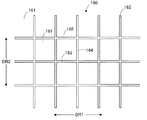
第1のスペーサーは、第1の方向に延びる第1の部分と、前記第1の方向とは異なる第2の方向に延び、かつ第1の部分と交差する第2の部分とを備える壁部と、壁部以外の領域に存在し、かつ光を通過させる光通過領域とを備えている。本明細書において、「第1の方向に延びる」とは、第1の部分を大局的に見たときに第1の部分が第1の方向に延びていれば足り、第1の方向に沿っている必要はない。また、同様に、「第2の方向に延びる」とは、第2の部分を大局的に見たときに第2の部分が第2の方向に延びていれば足り、第2の方向に沿っている必要はない。第1のスペーサー60は、図5に示されるように、第1のスペーサー60の高さ方向に貫通する2以上の光透過性領域としての開口部61と、開口部61間を仕切り、かつ少なくとも1つの開口部61の周囲を取り囲む壁部62とを有している。
A first spacer includes a first portion extending in a first direction, and a wall portion including a second portion extending in a second direction different from the first direction and intersecting the first portion. And a light passing area which is present in an area other than the wall and which allows light to pass. In the present specification, “extending in the first direction” means that it is sufficient if the first portion extends in the first direction when the first portion is viewed generally, along the first direction. It does not have to be Similarly, “extending in the second direction” means that it is sufficient if the second portion extends in the second direction when the second portion is viewed generally, along the second direction. It does not have to be The
<開口部>
開口部61は、各LED素子42からの光を通過させるためのものである。開口部61の個数は特に限定されないが、図5においては、LED素子42の個数(縦4個×横6個=24個)に対応して、縦4個×横6個=24個の開口部61が形成されている。<Aperture>
The
各開口部61は、各LED素子42からの光を通過させるものであるので、各開口部61は、第1のスペーサー60を平面視したとき、開口部61内にLED素子42が入る大きさとなっている。図6においては、1つの開口部61内に1個のLED素子42が配置されているが、1つの開口部内に複数個のLED素子が配置されていてもよい。
Since each
図5に示される開口部61は、全て同じ大きさとなっているが、開口部61は同じ大きさである必要はなく、異なる大きさであってもよい。
The
<壁部>
壁部62は、第1の方向DR1に延びる第1の部分63と、第1の方向DR1とは異なる第2の方向DR2に延び、かつ第1の部分63と交差する第2の部分64とを備えている。第1の部分63および第2の部分64は、壁部62の構成要素であり、具体的には、開口部61間を仕切る後述する仕切部66を構成する要素である。第1の部分と第2の部分は交差しているが、第1の部分と第2の部分のなす角度は、第1の光学シートを安定的に支持する観点から、60°以上であることが好ましい。本明細書においては、「第1の部分と第2の部分とのなす角度」とは、第1の部分と第2の部分のなす角度のうち小さい方の角度を意味するものとする。具体的には、第1のスペーサー60の場合、第1の部分63と第2の部分64のなす角度とは図5に示されるθ1で表される角度であり、また後述する第1のスペーサー140の場合、第1の部分143と第2の部分144のなす角度とは図7に示されるθ1で表される角度である。<Wall part>
The
壁部62は、上記したように、開口部61間を仕切り、かつ少なくとも1つの開口部61の周囲を取り囲んでいる。壁部62は、2以上の開口部61の周囲を取り囲んでいることが好ましく、全ての開口部61の周囲を取り囲んでいることがより好ましい。図5に示される壁部62は、格子状となっており、全ての開口部61の周囲を囲んでいる。本明細書における「格子状」とは、第1のスペーサーの平面視において、壁部によって複数の開口部がマトリクス状に配置された構造を意味するものとする。第1のスペーサーの平面視における開口部の形状としては、四角形状等の多角形状、楕円形状、円形状等が挙げられる。上記四角形状としては、正方形状、長方形状、菱形形状等が挙げられる。図5に示される第1のスペーサー60においては、壁部62によって四角形状の開口部61がマトリクス状に配置されている。壁部62は、射出成形、切削や三次元プリンターによって得ることができる。
The
壁部62は、格子状となっているが、壁部は、格子状となっていなくともよい。例えば、壁部は、開口部が千鳥状に配置されたものであってもよい。具体的には、図7に示される第1のスペーサー140のように、壁部142がハニカム状となったものでもよい。図7に示される第1のスペーサー140も、第1のスペーサー60と同様に、光通過領域としての2以上の開口部141を備えている。壁部142は、第1の方向DR1に延びる第1の部分143と、第1の方向DR1とは異なる第2の方向DR2に延び、かつ第1の部分143と交差する第2の部分144とを備えており、また壁部142は、開口部141間を仕切り、かつ少なくとも1つの開口部141の周囲を取り囲んでいる。第1のスペーサー140は、壁部142がハニカム状となっている以外、第1のスペーサー60と同様となっているので、ここでは説明を省略するものとする。なお、LED素子42がマトリクス状に配置されたLED実装基板40を用いる場合には、壁部62が格子状となった第1のスペーサー60を用い、LED素子が千鳥状に配置されたLED実装基板を用いる場合には、壁部142がハニカム状となった第1のスペーサー140を用いることができる。
The
また、図8に示される第1のスペーサー150のように、壁部152の開口部151側の角部152Aは、第1のスペーサー150の平面視において、曲線状となっていてもよい。角部152Aが、第1のスペーサー150の平面視において、曲線状になっていることにより、壁部152に振動や衝撃が加わった場合であっても、壁部152が割れにくくなるとともに、角部152Aにおける反射回数を低減させることができるので、輝度の低下を抑制できる。図8に示される第1のスペーサー150も、第1のスペーサー60と同様に、光通過領域としての2以上の開口部151を備えている。壁部152は、第1の方向DR1に延びる第1の部分153と、第1の方向DR1とは異なる第2の方向DR2に延び、かつ第1の部分153と交差する第2の部分154とを備えており、また壁部152は、開口部151間を仕切り、かつ少なくとも1つの開口部151の周囲を取り囲んでいる。第1のスペーサー150は、壁部152の角部152Aが曲線状になっている以外、第1のスペーサー60と同様となっているので、ここでは説明を省略するものとする。
Further, as in the
図5に示される壁部62は、枠部65と、枠部65よりも内側に位置し、開口部61間を仕切る仕切部66とから構成されている。壁部62は、枠部65を備えているが、例えば、図9に示される第1のスペーサー160のように、壁部162は、枠部を備えず、仕切部165のみから構成された井桁状となっていてもよい。図9に示される第1のスペーサー160も、第1のスペーサー60と同様に、光通過領域としての2以上の開口部161を備えている。壁部162は、第1の方向DR1に延びる第1の部分163と、第1の方向DR1とは異なる第2の方向DR2に延び、かつ第1の部分163と交差する第2の部分164とを備えており、また壁部162は、開口部161間を仕切り、かつ少なくとも1つの開口部161の周囲を取り囲んでいる。ただし、図9においては、壁部162は、最外周に存在する開口部161の周囲は取り囲んでいない。第1のスペーサー160は、壁部162が仕切部165のみから構成されている以外、第1のスペーサー60と同となっているので、ここでは説明を省略するものとする。
The
(枠部)
枠部65は、平面視において四角形状となっているが、枠部の形状は、LED実装基板の形状等に合わせて、適宜変更することができる。枠部65は、ほぼ配線基板41の大きさと同じ大きさになっている。(Frame part)
The
(仕切部)
仕切部66は、開口部61間を仕切るものである。図5に示される仕切部66は、枠部65と一体的に設けられていることが好ましい。仕切部66を枠部65と一体形成することによって、繋ぎ目がない第1のスペーサーを得ることができるので、第1のスペーサーを複数の部材から構成するよりも、面光源装置の組立工程の簡素化、および振動試験における第1の光学シートの位置ずれリスクの低減を図ることができる。また、第1のスペーサーには、繋ぎ目がないので、継ぎ目に入り込む光にもなく、光学的損失の低減を図ることができる。本明細書における「一体的に設けられている」とは、枠部と仕切部との間に境界が存在しない場合、すなわち枠部と仕切部が一体形成されている場合のみならず、仕切部が枠部に接合されている場合をも含む概念である。第1のスペーサー60においては、枠部65および仕切部66が一体形成されている。なお、壁部62の強度を高める観点から、仕切部66は枠部65と一体的に設けられていることが好ましいが、仕切部は枠部と一体的に設けられていなくともよい。(Partial division)
The
仕切部66は、図6に示されるように、区画領域51間の境界部51Cに対応する位置に配置されていることが好ましい。本明細書における「区画領域間の境界部」とは、透過部および反射部のパターンから区画領域間の境界と想定される領域を含む部分を意味するものとする。なお、図6は、LED素子42側から第1のスペーサー60および第1の光学シート50を平面視した図である。
It is preferable that the
壁部62の厚みは、0.2mm以上10mm以下であることが好ましい。壁部62の厚みが、0.2mm以上であれば、第1の光学シート50の支持体としての機能を確実に果たすことができ、また10mm以下であれば、開口部61の開口径を充分に確保することができるので、輝度低下を抑制できる。本明細書における「壁部の厚み」とは、壁部のうち最も薄い箇所の厚みを意味するものとする。壁部62の厚みは、全て均一でなくともよい。なお、壁部62を構成する枠部65と仕切部66の厚みは、同一であってもよいが、同一でなくともよい。壁部62の厚みの下限は、0.5mm以上であることがより好ましい。
The thickness of the
図3に示されるように、壁部62の開口部61に面している側面62Aが、第1のスペーサー60の高さ方向における底面60Aから上面60Bに向けて開口部61の開口径が大きくなるように傾斜している。このような側面62Aを有する壁部62を形成することにより、LED素子42からの出射光を壁部62の側面62Aで反射させて、第1の光学シート50に導くことができるので、面光源装置20からより効率良く光を出射させることができる。このような側面62Aを有する壁部62を備える第1のスペーサー60は、例えば、射出成形、切削や三次元プリンターによって得ることができる。側面62Aは、第1のスペーサー60の高さ方向の断面において、曲線状となっていてもよいが、作製し易さの観点から、直線状となっていることが好ましい。また、壁部は、第1のスペーサーの上面から底面に向けて開口部の開口径が大きくなるように傾斜していてもよい。
As shown in FIG. 3, the
壁部62の側面62Aは、粗面であることが好ましい。具体的には、例えば、側面62Aの算術平均粗さRaは、0.1μm以上100μm以下であることが好ましい。側面62AのRaが、0.1μm以上であれば、拡散反射が多くなるので、輝度の面内均一性をより向上させることができ、100μm以下であれば、反射回数が増えすぎないので、第1のスペーサー60が光を吸収する頻度が高まることを抑制でき、輝度の面内均一性の低下を抑制できる。Raは、JIS B0601:1999に準拠して、表面粗さ測定装置(製品名「SE−3400」、株式会社小坂研究所製)を用いて測定することができる。Raは、ランダムに10箇所測定し、測定した10箇所のRaの算術平均値とする。側面62Aを粗面化する方法としては、特に限定されないが、壁部62に後述する粒子を含有させる方法またはサンドブラスト法が挙げられる。
The
壁部62は、LED素子42からの光を反射して第1の光学シート50に導く観点から、光反射性を有することが好ましい。壁部62を構成する材料としては、特に限定されないが、成形し易く、また第1の光学シート50等を衝撃から保護する観点から、樹脂(第1の樹脂)から構成されていることが好ましい。第1の樹脂の中でも、反射率を高めて、第1の光学シート50に光を導く観点から白色系樹脂等の光反射性樹脂が好ましい。壁部62は、光拡散性を向上させる観点から、樹脂の他、粒子をさらに含んでいることが好ましい。また、LED素子42からは可視光線のみならず紫外線も放射しているので、面光源装置20内の部材が紫外線により劣化するおそれがある。このため、壁部62は、紫外線劣化を抑制するために、樹脂の他、紫外線吸収剤をさらに含んでいることが好ましい。
The
上記第1の樹脂の25℃でのヤング率は、0.5GPa以上5GPa以下であることが好ましい。第1の樹脂のヤング率が、0.5GPa未満であると、壁部において、配線基板や第1の光学シートを固定するための強度が確保できないおそれがあり、また5GPaを超えると、面光源装置を曲面などへ設置する際に第1のスペーサーを曲げることができないおそれがある。第1の樹脂の25℃でのヤング率の下限は、1GPa以上であることがより好ましく、上限は4GPa以下であることがより好ましい。 The Young's modulus at 25 ° C. of the first resin is preferably 0.5 GPa or more and 5 GPa or less. If the Young's modulus of the first resin is less than 0.5 GPa, there is a possibility that the strength for fixing the wiring substrate or the first optical sheet can not be secured in the wall portion, and if it exceeds 5 GPa, a surface light source There is a possibility that the first spacer can not be bent when installing the device on a curved surface or the like. The lower limit of the Young's modulus at 25 ° C. of the first resin is more preferably 1 GPa or more, and the upper limit is more preferably 4 GPa or less.
上記第1の樹脂としては、ポリカーボネート樹脂、アクリロニトリル−ブタジエン−スチレン共重合樹脂(ABS樹脂)、アクリロニトリル−スチレン−アクリレート共重合樹脂(ASA樹脂)、アクリロニトリル−ブタジエン−スチレン共重合樹脂(AES樹脂)、ポリメチルメタクリレート樹脂(PMMA樹脂)、ポリアセタール樹脂、ポリ塩化ビニル樹脂、ポリエチレン樹脂、ポリプロピレン樹脂、ポリエチレンテレフタレート樹脂、またはこれらの樹脂を2種以上混合した混合物等が挙げられる。これらの中でも、耐熱性や成形性等の観点から、ポリカーボネート樹脂、ABS樹脂、ASA樹脂、AES樹脂、PMMA樹脂、ポリアセタール樹脂、またはこれらの樹脂を2種以上混合した混合物が好ましい。 Examples of the first resin include polycarbonate resin, acrylonitrile-butadiene-styrene copolymer resin (ABS resin), acrylonitrile-styrene-acrylate copolymer resin (ASA resin), acrylonitrile-butadiene-styrene copolymer resin (AES resin), Polymethyl methacrylate resin (PMMA resin), polyacetal resin, polyvinyl chloride resin, polyethylene resin, polypropylene resin, polyethylene terephthalate resin, or a mixture of two or more of these resins can be mentioned. Among these, polycarbonate resins, ABS resins, ASA resins, ASA resins, AES resins, PMMA resins, polyacetal resins, or a mixture of two or more of these resins is preferable from the viewpoint of heat resistance and moldability.
上記粒子としては、無機粒子が挙げられる。無機粒子としては、例えば、シリカ、アルミナ、チタニア(TiO2)、酸化スズ、アンチモンドープ酸化スズ(ATO)、酸化亜鉛微粒子等の無機酸化物粒子が挙げられる。第1のスペーサー60中に粒子は、第1の樹脂100質量部に対して10質量部以上250質量部以下の割合で含まれていることが好ましい。Examples of the particles include inorganic particles. Examples of the inorganic particles include inorganic oxide particles such as silica, alumina, titania (TiO 2 ), tin oxide, antimony-doped tin oxide (ATO), and zinc oxide fine particles. The particles are preferably contained in the
上記紫外線吸収剤としては、特に限定されず、トリアジン系紫外線吸収剤やベンゾトリアゾール系紫外線吸収剤が挙げられる。これらの中でも、可視光領域の光は極力吸収せず、効率的に紫外線を吸収することができるとともに、長期間使用しても黄変が生じにくい観点から、トリアジン系紫外線吸収剤が好ましい。トリアジン系紫外線吸収剤の市販品としては、例えば、BASF社製のTINUVIN 1577 EDが挙げられる。また、必要に応じて、ヒンダードアミン系光安定剤等を添加してもよい。 It does not specifically limit as said ultraviolet absorber, A triazine type ultraviolet absorber and a benzotriazole type ultraviolet absorber are mentioned. Among these, triazine-based ultraviolet absorbers are preferable from the viewpoint of not absorbing light in the visible light region as much as possible, and capable of efficiently absorbing ultraviolet light and hardly causing yellowing even when used for a long period of time. As a commercial item of a triazine series ultraviolet absorber, BASF Corporation TINUVIN 1577 ED is mentioned, for example. Moreover, you may add a hindered amine light stabilizer etc. as needed.
壁部62は、帯電防止性を有していることが好ましい。面光源装置の製造時や使用時に埃が付着すると、故障の原因となるが、壁部62が帯電防止性を有することによって、面光源装置の製造時や使用時に埃が付着することを抑制できる。帯電防止性は表面抵抗値で表すことが可能であるので、壁部62が帯電防止性を有する場合、壁部62の表面抵抗値は、1012Ω/□以下となっていることが好ましい。表面抵抗値は、JIS K6911:2006に準拠して、抵抗率計(製品名「ハイレスタ−UP MCP−HT450」、株式会社三菱化学アナリテック製、プローブ:URS)を用いて、測定することができる。壁部62の表面抵抗値は、壁部62の表面抵抗値をランダムに10箇所測定し、測定した10箇所の表面抵抗値の算術平均値とする。壁部62に帯電防止性を付与する方法としては、帯電防止剤を含む組成物をスプレーや浸漬によりコーティングする方法が挙げられる。The
壁部62のガラス転移温度(Tg)は、85℃を越えることが好ましい。自動車等の車両に面光源装置を組み込む場合には、エンジン等によって加熱されるので、壁部62は、壁部62に対し85℃で1000時間放置する環境試験を行った場合であっても、流動しないことが必要とされる。壁部62のガラス転移温度が85℃を越えるものであれば、壁部62に対し85℃の環境下で1000時間放置する環境試験を行った場合であっても、壁部62の流動を抑制できる。また、夏場には環境試験以上の熱が加わるおそれがあるので、夏場を考慮すると、壁部62のガラス転移温度は、115℃を越えることがより好ましい。ここで、面光源装置は、非常に薄型であるため、第1の光学シートとLED実装基板との間の距離は非常に精密に設計されており、仮に、壁部が、流動してしまうと、第1の光学シートとLED実装基板との間の距離が変化してしまうので、輝度ムラが発生して、輝度の面内均一性が低下してしまう。このことから、壁部62の耐熱信頼性は非常に重要である。壁部62のガラス転移温度は、壁部62を10mg削り取ってサンプルとし、示差走査熱量計(DSC)を用いて、昇温速度5℃/minの条件で測定するものとする。壁部62のガラス転移温度は、3回測定した値の算術平均値とする。なお、壁部62のガラス転移温度が2以上確認されたときには、ガラス転移温度としては、最も低い温度のガラス転移温度を採用するものとする。
Preferably, the glass transition temperature (Tg) of the
壁部62の成形収縮率は、1.0%未満であることが好ましい。壁部62の成形収縮率が1.0%未満であれば、成形後の冷却時における壁部62の寸法変化および反りの発生等を抑制することができる。壁部62の成形収縮率の測定は、JIS K6911:1995に基づいて行うが、壁部62の成形収縮率の測定の際には、壁部62を加熱することによって壁部62を構成する樹脂を溶融させて、この樹脂を金型に流し込み、固化させることによって得た成形物を用いるものとする。
The molding shrinkage of the
壁部62においては、枠部65と仕切部66が一体的に設けられているが、枠部65と仕切部66を一体的に設けられなくともよい。すなわち、図10(A)に示される第1のスペーサー170のように、枠部175と仕切部176を別々に作製し、枠部175の内側に仕切部176を配置して壁部172を得てもよい。また、図10(B)に示される第1のスペーサー180のように2以上の壁部182A同士を接合して、壁部182を得てもよい。なお、第1のスペーサー170、180においても、壁部172、182の他、光通過領域である2以上の開口部171、181を備えており、また壁部172、182は、第1の方向DR1に延びる第1の部分173、183と、第2の方向DR2に延び、かつ第1の部分173、183と交差する第2の部分174、184とを備えている。
Although the
また、壁部62においては、第1の部分63が第1の方向DR1に連続的に延びており、第2の部分64が第2の方向DR2に連続的に延びているが、第1の部分や第2の部分は、複数の分割片から構成されていてもよい。本明細書においては、第1の部分や第2の部分が複数の分割片から構成されている場合には、第1の方向に並んだ複数の分割片の集合体を第1の部分とし、第2の方向に並んだ複数の分割片の集合体を第2の部分とする。第1の部分や第2の部分が複数の分割片から構成されている場合には、第1の部分や第2の部分を分割片の集合体として見たときに、第1の部分と第2の部分が交差していればよく、第1の部分を構成する分割片と第2の部分を構成する分割片とは必ずしも交差していなくともよい。
In the
第1の部分や第2の部分が複数の分割片から構成された第1のスペーサーとしては、例えば、図11(A)、図11(B)、図12(A)および図12(B)に示される第1のスペーサー190、200、210、220が挙げられる。第1のスペーサー190、200、210、220は、第1のスペーサー60と同様に、それぞれ、光通過領域191、201、211、221と、第1の方向DR1に延びる第1の部分193、203、213、223と、第1の方向DR1とは異なる第2の方向DR2に延び、かつ第1の部分193、203、213、223と交差する第2の部分194、204、214、224とを備える壁部192、202、212、222とを備えている。なお、図11(A)、図11(B)、図12(A)および図12(B)においては、第1の部分193、203、213、223および第2の部分194、204、214、224を二点鎖線で示している。
Examples of the first spacer in which the first portion and the second portion are formed of a plurality of divided pieces include, for example, FIG. 11 (A), FIG. 11 (B), FIG. 12 (A) and FIG. 12 (B). The
図11(A)に示される第1のスペーサー190においては、第1の部分193は複数の分割片193Aから構成されており、第2の部分194は複数の分割片194Aから構成されており、分割片193Aと分割片194Aはそれぞれ直接交差している。
In the
第1のスペーサー190においては、第1の方向D1において任意の分割片193Aと分割片194Aとの第1の交点から隣の分割片193Aと分割片194Aとの第2の交点までの距離を100%としたとき、第1の交点と第2の交点との間に分割片193Aの占める長さの割合が50%以上となるように分割片193Aが存在していることが好ましい。例えば、第1の交点を構成する分割片193Aは第1の交点から第2の交点に向けて25%以上の長さで延びており、かつ第2の交点を構成する分割片193Aは第2の交点から第1の交点に向けて25%以上の長さで延びていることが好ましい。分割片193Aの長さをこのような長さにすることによって、第1の部分193を複数の分割片193から構成した場合であっても、第1の光学シート50との接触面積の低下を抑制できる。同様の理由から、第1のスペーサー190においては、第2の方向D2において任意の分割片193Aと分割片194Aとの第1の交点から隣の分割片193Aと分割片194Aとの第2の交点までの距離を100%としたとき、第1の交点と第2の交点との間に分割片193Aの占める長さの割合が50%以上となるように分割片194Aが存在していることが好ましい。例えば、第1の交点を構成する分割片194Aは第1の交点から第2の交点に向けて25%以上の長さで延びており、かつ第2の交点を構成する分割片194Aは第2の交点から第1の交点に向けて25%以上の長さで延びていることが好ましい。
In the
図11(B)に示される第1のスペーサー200においては、第1の部分203は複数の分割片203A、203Bから構成されており、第2の部分204は複数の分割片204A、204Bから構成されている。分割片203Aと分割片204Aはそれぞれ直接交差しているが、分割片203A間に存在する分割片203Bは分割片204A、204Bと交差しておらず、また分割片204A間に存在する分割片204Bは分割片203A、203Bと交差していない。
In the
第1のスペーサー200においても、上記と同様の理由から、第1の方向D1において任意の分割片203Aと分割片204Aとの第1の交点から隣の分割片203Aと分割片204Aとの第2の交点までの距離を100%としたとき、第1の交点と第2の交点との間に分割片203A、203Bの占める合計の長さの割合が50%以上となるように分割片203A、203Bが存在していることが好ましく、第2の方向D1において任意の分割片203Aと分割片204Aとの第1の交点から隣の分割片203Aと分割片204Aとの第2の交点までの距離を100%としたとき、第1の交点と第2の交点との間に分割片204A、204Bの占める合計の長さの割合が50%以上となるように分割片204A、204Bが存在していることが好ましい。
Also in the
図12(A)および図12(B)に示される第1のスペーサー210、220においては、第1の部分213、223は、それぞれ複数の分割片213A、223Aから構成されており、第2の部分214、224は、それぞれ複数の分割片214A、224Aから構成されている。分割片213A、223Aと分割片214A、224Aは直接交差していないが、第1の方向DR1に並んだ複数の分割片213A、223Aの集合体からなる第1の部分213、223と、第2の方向DR2に並んだ複数の分割片214A、224Aの集合体からなる第2の部分214、224は交差している。本明細書においては、図12(B)のように分割片自体が第1の方向や第2の方向に延びているとは言えない場合であっても、第1の部分と第2の部分の任意の交点から第1の方向における隣の交点までの間に交点を構成しない分割片が少なくとも1以上存在していれば、第1の部分が第1の方向に延びているとみなし、また第1の部分と第2の部分の任意の交点から第2の方向における隣の交点までの間に交点を構成しない分割片が少なくとも1以上存在していれば、第2の部分が第2の方向に延びているとみなすものとする。
In the
壁部の第1の光学シート側の上面には、第2の実施形態で詳細に説明するように凸部が設けられていてもよい。第1のスペーサーは、上記したように、射出成形、打ち抜き、切削、または三次元プリンターによって作製することが可能であるが、第1のスペーサーに凸部を設ける場合には、これらの中でも、凸部の形成し易さの観点から、射出成形が好ましい。 As described in detail in the second embodiment, a convex portion may be provided on the upper surface of the wall portion on the first optical sheet side. As described above, the first spacer can be manufactured by injection molding, punching, cutting, or a three-dimensional printer, but in the case where the first spacer is provided with a convex portion, among these, the convex may be formed. Injection molding is preferred from the viewpoint of ease of formation of the part.
面光源装置においては、第1の光学シートの撓みを抑制する等の観点から、壁部を有する第1のスペーサーを設けているが、壁部は少なからず光を吸収する性能を有しているので、壁部に到達する度に光吸収が生じてしまい、また壁部に含有された反射率を高めるための粒子で拡散反射されることが影響して、柱状のスペーサーや枠状のスペーサーよりも輝度が低下してしまうおそれがある。このため、輝度向上の観点から、仕切部には、仕切部の幅方向に貫通する開口部を形成することが好ましい。具体的には、図13(A)、図13(B)、図14(A)および図14(B)に示されるように、仕切部230、240、250、260は、第1の仕切部231、241、251、261と、第1の仕切部231、241、251、261と隣り合う第2の仕切部232、242、252、262と、第1の仕切部231、241、251、261および第2の仕切部232、242、252、262と交差し、かつ第1の仕切部231、241、251、261と第2の仕切部232、242、252、262との間に第2の開口部233A、243A、253A、263A(以下、単に開口部233A、243A、253A、263Aと称することもある。)を有する第3の仕切部233、243、253、263とを備えていてもよい。第2の仕切部232、242、252、262は、開口部234、244、254、264を介することにより第1の仕切部231、241、251、261と離間している。第3の仕切部233、243、253、263に開口部233A、243A、253A、263Aを有することにより、LED素子42から発せられる一部の光は、開口部233A、243A、253A、263Aを介して隣の開口部側に抜けるので、第3の仕切部233、243、253、263による光吸収をより低減でき、輝度低下をより抑制できる。第2の開口部は、貫通孔であってもよく、また切り欠きであってもよい。図13(A)等に示される開口部233A、243A、253A、263Aは、切り欠きとなっている。なお、開口部233A、243A、253A、263Aは第3の仕切部233、243、253、263に形成されているが、第1の仕切部231、241、251、261および第2の仕切部232、242、252、262にも開口部233A、243A、253A、263Aと同様の開口部が形成されていることが好ましい。
In the surface light source device, the first spacer having the wall portion is provided from the viewpoint of suppressing the bending of the first optical sheet, etc., but the wall portion has the ability to absorb light not a little. Therefore, light absorption occurs every time it reaches the wall, and it is affected by diffuse reflection by the particles contained in the wall to increase the reflectance, and it is more likely than columnar spacers or frame-like spacers. Also, the brightness may be reduced. For this reason, it is preferable to form an opening penetrating in the width direction of the partition in the partition from the viewpoint of improving the brightness. Specifically, as shown in FIGS. 13 (A), 13 (B), 14 (A) and 14 (B), the
図13(A)、図13(B)、図14(A)および図15(B)に示されるように、第3の仕切部233、243、253、263の延在方向EDおよび第1スペーサーの高さ方向HDの両方に沿った断面において、第3の仕切部233、243、253、263および開口部233A、243A、253A、263Aの合計面積AR(二点鎖線で囲まれた面積)に対する開口部233A、243A、253A、263Aの面積の割合である仕切部開口率は、30%以上70%以下であることが好ましい。この仕切部開口率が30%以上であれば、仕切部230、240、250、260による光吸収をより抑制できるので、輝度低下をより抑制でき、またこの仕切部開口率が70%以下であれば、所望の強度を維持できるので、第1の光学シート50の支持体としての機能を確実に果たすことができる。第3の仕切部の面積は、第1の仕切部との交差部から第2の仕切部との交差部までの面積とし、また図13(A)等のように第2の開口部が第1のスペーサーの高さ方向において開放している切り欠きの場合には、第2の開口部の面積は、第1のスペーサーに対し第2の開口部の開口している側に平板を接触させ、平板と第3の仕切部との間の空間の面積とする。また、第3の仕切部に設けられた第2の開口部の形状が第3の仕切部の幅方向で変化している場合には、第3の仕切部および第2の開口部の合計面積および第2の開口部の面積は、第2の開口部の面積が最も小さくなる位置の断面で、第3の仕切部および第2の開口部の合計面積および第2の開口部の面積を求めるものとする。
As shown in FIGS. 13 (A), 13 (B), 14 (A) and 15 (B), the extending direction ED of the
図13(A)においては、開口部233Aは仕切部230の底面230A側に位置しており、また第3の仕切部233における開口部233A側の底面233Bは平面状となっているが、図13(B)に示されるように第3の仕切部243における開口部243A側の底面243Bは、例えば、アーチ状のような曲面状になっていてもよい。また、図14(A)および図14(B)に示されるように、開口部253A、263Aは仕切部250、260の底面250A、260Aとは反対側の上面250B、260B側に位置していてもよい。また図13(A)においては、第3の仕切部233には第1の仕切部231と第2の仕切部232との間に1つの開口部233Aが設けられているが、第1の仕切部と第2の仕切部との間に2以上の開口部を設けてもよい。また、図13(A)においては、上記断面において、スペーサーの高さ方向に沿った開口部233Aの中心線に対して左右対称となるように開口部233Aが形成されているが、開口部は左右非対称であってもよい。
In FIG. 13A, the
壁部における第1の部分と第2の部分との交差部においては、第1のスペーサーの密度が高く、かつLED素子の距離が離れているので、暗くなりやすい。このため、第1の部分と第2の部分との交差部付近の輝度向上の観点から、交差部を第1の光学シート側から削り、図15に示されるように第1の部分272と第2の部分273との交差部に、交差部に隣接する光通過領域271のうち2以上の光通過領域271が一部において繋がるように切欠き274を形成することが好ましい。第1の部分272と第2の部分273との交差部にこのような切欠き274を形成することによって、交差部からも光を出射させることができるので、交差部付近の輝度を向上させることができる。
At the intersection of the first portion and the second portion in the wall, the density of the first spacer is high, and the distance between the LED elements is large, so it tends to be dark. Therefore, from the viewpoint of improving the brightness in the vicinity of the intersection between the first part and the second part, the intersection is cut from the side of the first optical sheet, and as shown in FIG. It is preferable to form a
<<第2の光学シート>>
第2の光学シート70は、光学的な機能を有するシートである。第2の光学シートとしては、光学的な機能を有するシートであれば、特に限定されず、例えば、光拡散シート、レンズシート、または反射型偏光分離シート等が挙げられる。図1および図2に示される第2の光学シート70は、光拡散シートとなっている。光拡散シートである第2の光学シート70を配置することにより、第1の光学シート50を透過した光を第2の光学シート70でさらに拡散させることができ、輝度の面内均一性をさらに向上させることができる。なお、第2の光学シートが、レンズシートである場合には、レンズシート90は備えなくともよく、また第2の光学シートが、反射型偏光分離シートである場合には、反射型偏光分離シート100は備えなくともよい。また、第2の光学シートとして、レンズシートや反射型偏光分離シートを用いる場合には、レンズシート90や反射型偏光分離シート100と同様のものを用いることができる。<< Second Optical Sheet >>
The second
第2の光学シート70は、第1の光学シート50の光出射側に配置されている。第2の光学シート70は、第2のスペーサー80によって第1の光学シート50に対し離間している。第2の光学シート70は、第1の光学シート50と略平行に配置されている。
The second
図3に示される第1の光学シート50から第2の光学シート70までの距離d2は、5mm以下であることが好ましい。5mmを超えると、面光源装置の薄型化が図れないおそれがある。本明細書における「第1の光学シートから第2の光学シートまでの距離」とは、第1の光学シートにおける第2の光学シート側の面から第2の光学シートにおける第1の光学シート側の面までの距離を意味するものとする。第1の光学シート50から第2の光学シート70までの距離は、この距離をランダムに10箇所測定した値の算術平均値とする。
The distance d2 from the first
面光源装置の薄型化を図る観点からは、距離d2は2mm以下(0mmを含む)であることが好ましい。ただし、この場合には、第1の光学シートにおける光拡散機能が十分に発揮されず、第2の光学シートを平面視すると、第1のスペーサーの上面に対応する部分が他の部分よりも暗くなってしまうおそれがある。したがって、距離d2を2mm以下にする場合には、第1のスペーサー60の壁部62の開口部61に面している側面62Aが、第1のスペーサー60の高さ方向における底面60Aから上面60Bに向けて開口部61の開口径が大きくなるように傾斜していることが好ましい。第1のスペーサー60の側面62Aがこのように傾斜していることにより、第1のスペーサー60の上面60Bに対応する部分が他の部分よりも暗くなることを抑制できる。距離d2を2mm以下(0mmを含む)にする場合には、第1のスペーサー60の底面60Aの幅に対する上面60Bの幅の比(上面の幅/底面の幅)は、0.95以下であることが好ましく、0.3以下であることがさらに好ましい。この比の下限は、第1の光学シート50を安定的に支持する観点から、0.1以上であることが好ましい。
From the viewpoint of reducing the thickness of the surface light source device, the distance d2 is preferably 2 mm or less (including 0 mm). However, in this case, the light diffusion function of the first optical sheet is not sufficiently exhibited, and the portion corresponding to the upper surface of the first spacer is darker than the other portions when the second optical sheet is viewed in plan. There is a risk of becoming Therefore, when the distance d2 is set to 2 mm or less, the
配線基板41の表面41Aから第2の光学シート70までの距離(OD)は、面光源装置20の薄型化を図る観点から、1mm以上10mm以下となっていることが好ましい。本明細書における「配線基板の表面から第2の光学シートまでの距離」とは、配線基板の表面から第2の光学シートにおける配線基板側の面までの距離を意味するものとする。配線基板41の表面41Aから第2の光学シート70までの距離は、この距離をランダムに10箇所測定した値の算術平均値とする。配線基板41の表面41Aから第2の光学シート70までの距離の上限は、5mm以下となっていることが好ましい。
The distance (OD) from the
第2の光学シート70の厚みは、第1の光学シート50の厚みよりも大きくなっていることが好ましい。第2の光学シート70の厚みが、第1の光学シート50の厚みより大きいことにより、第2の光学シート70は、第1の光学シート50よりも撓み難い。このため、第2の光学シート70は、枠状の第2のスペーサー80によって、第1の光学シート50と第2の光学シート70との間の距離を所定の距離に保持することができる。
The thickness of the second
第2の光学シート70の厚みは、0.3mm以上5mm以下であることが好ましい。第2の光学シート70の厚みが、0.3mm未満であると、光拡散効果が十分に得られないおそれがあるからであり、また厚みが、5mmを超えると、面光源装置の薄型化が図れないおそれがある。第2の光学シート70の厚みは、第1の光学シート50の厚さと同様の方法によって測定することができる。
The thickness of the second
第2の光学シート70は、樹脂から構成されていることが好ましい。本明細書における「樹脂から構成されている」とは、樹脂が主の構成成分となっていることを意味する。第2の光学シート70は、ポリカーボネート樹脂やアクリル樹脂等からなる半透明の樹脂フィルムと、樹脂フィルムの一方の面側に形成された、光拡散機能を発揮するための、例えば、微小でランダムなレンズアレイ等を有するレンズ層とを備えている。
The second
<<第2のスペーサー>>
第2のスペーサー80は、第1の光学シート50に対し第2の光学シート70を離間させるためのものである。また、第2のスペーサー80は、第1の光学シート50から第2の光学シート70までの距離d2を0.5mm以上5mm以下に保持するとともに、配線基板41の表面41Aから第2の光学シート70までの距離を1mm以上10mm以下に保持する機能を有している。<< Second Spacer >>
The
図3に示される第2のスペーサー80の高さh2は、第1のスペーサー60の高さh1よりも大きくなっている。第2のスペーサー80の高さh2は、1mm以上10mm以下であることが好ましい。第2のスペーサーの高さが、1mm未満であると、第1の光学シートと第2の光学シートとの距離が短すぎるために、第2の光学シートの平面視において、第1の光学シートの各区画領域の中央部に対応する部分が外縁部に対応する部分よりも明るくなるおそれがあり、また10mmを越えると、面光源装置の薄型化が図れないというおそれがある。本明細書における「第2のスペーサーの高さ」とは、第2のスペーサーにおける筐体の内底面側の面である底面に垂直な方向において、第2のスペーサーの底面から第2のスペーサーの上面までの距離を意味するものとする。第2のスペーサー80の高さh2は、第2のスペーサー80の高さをランダムに10箇所測定した値の算術平均値とする。
The height h 2 of the
第2のスペーサー80は、図16に示されるように、枠状となっている。本明細書の「枠状」とは、切れ間なく1周繋がっている構成のみならず、概ね繋がっていれば途中で切れ間があってもよい。図16に示される第2のスペーサー80は、端子等との接続のために、切れ間80Aが設けられている。第2のスペーサー80は、1つの開口部81を有しており、第1の光学シート50の外周面50Aおよび第1のスペーサー60の外周面60Cを取り囲むように配置されている。第2のスペーサー80は、図2に示されるように、第1の光学シート50の外周面50Aおよび第1のスペーサー60の外周面60Cのみならず、配線基板41の外周面41Cを取り囲むように配置されている。すなわち、第2のスペーサー80の内側には、LED実装基板40、第1の光学シート50、および第1のスペーサー60が位置している。第2のスペーサー80が枠状になっていることにより、第1の光学シート50を透過して、第2のスペーサー80側に向かう光を第2のスペーサー80で反射させて、第2の光学シート70に導くことができる。また、第2のスペーサー80が枠状となっていることにより、第2のスペーサーが複数の柱状体から構成されている場合よりも、第2の光学シート70との接触面積を増大させることができるので、面光源装置20の使用時において、第2のスペーサー80を介して第2の光学シート70の熱をより放熱させることができる。また、第2のスペーサー80が枠状となっていることにより、第2のスペーサーが複数の柱状体から構成されている場合よりも、第2のスペーサー80と第2の光学シート70との接着面積を増大させることができるので、より第2の光学シート70が位置ずれしにくい。
The
図3に示されるように、第2のスペーサー80の底面80Bは筐体30の内底面30Bに接していることが好ましい。本明細書における「第2のスペーサーの底面が筐体の内底面と接している」とは、第2のスペーサーの底面が筐体の内底面に直接接触している場合に限らず、第2のスペーサーの底面と筐体の内底面との間に、両面テープ、粘着剤または接着剤等、熱伝導という観点でほぼ無視できる層が介在している場合をも含む概念である。図3においては、第2のスペーサー80の底面80Bと筐体30の内底面30Bとの間には、後述する両面テープ113が介在している。
As shown in FIG. 3, the
また、図3に示される第2のスペーサー80の外側の側面である外側面80Cは筐体30の内側面30Dに接している。本明細書における「第2のスペーサーの外側面」とは、第2のスペーサーの開口部を画定する内側面とは反対側の面を意味するものとする。また、本明細書における「第2のスペーサーの外側面が筐体の内側面と接している」とは、第2のスペーサーの外側面が筐体の内側面に直接接触している場合に限らず、第2のスペーサーの外側面と筐体の内側面との間に、両面テープ、粘着剤または接着剤等、熱伝導という観点でほぼ無視できる層が介在している場合をも含む概念である。図3においては、第2のスペーサー80の外側面80Cは、筐体30の内側面30Dに直接接している。
Further, an
第2のスペーサー80と筐体30は、LED素子42に対する第2の光学シート70の位置ずれをより抑制する観点から、固定されていることが好ましい。第2のスペーサー80と筐体30の固定方法としては、特に限定されず、接着や機械的固定手段による固定が挙げられる。図3においては、第2のスペーサー80の底面80Bと筐体30の内底面30Bが、両面テープ113を介して接着されることによって固定されている。ここで、第2のスペーサー80は、枠状となっているので、第2のスペーサーが複数の柱状体から構成されている場合よりも、筐体30との接着面積を増大させることができるので、第2のスペーサー80を固定しやすい。なお、第2のスペーサー80と筐体30は、両面テープ113ではなく、接着剤や粘着剤を介して接着されていてもよい。
The
第2のスペーサー80と第2の光学シート70は、固定されていることが好ましい。第2のスペーサー80と第2の光学シート70の固定方法としては、特に限定されず、接着や機械的固定手段による固定が挙げられる。図3においては、第2のスペーサー80における底面80Bとは反対側の上面80Dと第2の光学シート70が、両面テープ114を介して接着されることによって固定されている。第2のスペーサー80と第2の光学シート70を固定することにより、LED素子42に対する第2のスペーサー80の位置ずれをより抑制できる。なお、第2のスペーサー80と第2の光学シート70は、両面テープ114ではなく、接着剤や粘着剤を用いて固定されていてもよい。
The
図3に示されるように、第2のスペーサー80の内側の側面である内側面80Eは、筐体30の内底面30Bから第2の光学シート70に向けて開口部81の開口径が大きくなるように傾斜していることが好ましい。このような内側面80Eを有する第2のスペーサー80を形成することにより、第1の光学シート50からの出射光を第2のスペーサー80の内側面80Eで反射させて、第2の光学シート70に導くことができるので、面光源装置20からより効率良く光を出射させることができる。このような内側面80Eを有する第2のスペーサー80は、例えば、射出成形、打ち抜き、切削または三次元プリンターによって得ることができる。内側面80Eは、第2のスペーサー80の高さ方向の断面において、曲線状となっていてもよいが、作製し易さの観点から、直線状となっていることが好ましい。
As shown in FIG. 3, the
第2のスペーサー80は、LED素子42からの光を反射して第2の光学シート70に導く観点から、光反射性を有することが好ましい。第2のスペーサー80を構成する材料としては、特に限定されないが、成形し易く、また第2の光学シート70等を衝撃から保護する観点から、樹脂(第2の樹脂)から構成されていることが好ましい。第2の樹脂の中でも、反射率を高めて、第2の光学シート70に光をより導く観点から白色系樹脂等の光反射性樹脂が好ましい。
The
第2のスペーサー80を構成する第2の樹脂は、第1のスペーサー60を構成する第1の樹脂と同じ樹脂であることが好ましい。ただし、現在、面光源装置を曲げることが望まれており、面光源装置を曲げるために、第1のスペーサーおよび第2のスペーサーをヤング率が低い樹脂から構成した場合には、面光源装置の剛性が低下してしまうので、面光源装置を曲げる場合には、ある程度の剛性を維持しながら、面光源装置が曲げられるように、第2のスペーサー80を構成する第2の樹脂の25℃でのヤング率は、第1のスペーサー60を構成する第1の樹脂の25℃でのヤング率よりも小さいことが好ましい。第1のスペーサー60を構成する第1の樹脂の25℃でのヤング率および第2のスペーサー80を構成する第2の樹脂の25℃でのヤング率は、それぞれ動的粘弾性測定装置(製品名「Rheogel-E4000」、株式会社ユービーエム製)を用いて、25℃で引張り試験を行い、縦軸に応力、横軸にひずみをとった応力−ひずみ曲線の直線部の傾きから求めるものとする。なお、上記ヤング率は、3回測定して得られた値の算術平均値とする。
It is preferable that the 2nd resin which comprises the
<<レンズシート>>
レンズシート90は、入射した光の進行方向を変化させて出光側から出射させる機能を有する。レンズシート90は、図17に示されるように、例えばL1のような入射角度が大きい光の進行方向を変化させて出光側から出射させて、正面方向の輝度を集中的に向上させる機能(集光機能)とともに、例えばL2のような入射角度が小さい光を反射させて、第2の光学シート70側に戻す機能(再帰反射機能)を有している。レンズシート90は、図17に示されるように、樹脂フィルム91と、樹脂フィルム91の一方の面に設けられたレンズ層92とを備えている。なお、レンズシート90は、レンズ層92が樹脂フィルム91よりも反射型偏光分離シート100側に位置するように配置されている。<< Lens sheet >>
The
(樹脂フィルム)
樹脂フィルム91の構成材料としては、例えば、ポリエステル(例えば、ポリエチレンテレフタレート、ポリエチレンナフタレート)、セルローストリアセテート、セルロースジアセテート、セルロースアセテートブチレート、ポリアミド、ポリイミド、ポリエーテルスルフォン、ポリスルフォン、ポリプロピレン、ポリメチルペンテン、ポリ塩化ビニル、ポリビニルアセタール、ポリエーテルケトン、ポリメタクリル酸メチル、ポリカーボネート、又は、ポリウレタン等の熱可塑性樹脂が挙げられる。(Resin film)
As a constituent material of the
(レンズ層)
レンズ層92は、出光側に並べて配置された複数の単位レンズ92Aを備えている。単位レンズ92Aは、三角柱状であってもよいし、波状や例えば半球状のような椀状であってもよい。具体的には、単位レンズとしては、単位プリズム、単位シリンドリカルレンズ、単位マイクロレンズ等が挙げられる。なお、そのような単位レンズ形状を有するレンズシートとしては、プリズムシート、レンチキュラーレンズシート、マイクロレンズシート等が挙げられる。(Lens layer)
The
単位レンズ92Aは、光の利用効率を向上させる観点から、80°以上100°以下の頂角θ2を有することが好ましく、約90°の頂角を有することがより好ましい。
The
<反射型偏光分離シート>
反射型偏光分離シート100は、レンズシート90から出射される光のうち、第1の直線偏光成分(例えば、P偏光)のみを透過し、かつ第1の直線偏光成分と直交する第2の直線偏光成分(例えば、S偏光)を吸収せずに反射する機能を有するものである。反射型偏光分離シート100で反射された第2の直線偏光成分は再度反射され、偏光が解消された状態(第1の直線偏光成分と第2の直線偏光成分とを両方含んだ状態)で、再度、反射型偏光分離シート100に入射する。<Reflective type polarization separation sheet>
Of the light emitted from the
反射型偏光分離シート100としては、3M社から入手可能な「DBEF」(登録商標)を用いることができる。また、「DBEF」以外にも、Shinwha Intertek社から入手可能な高輝度偏光シート「WRPS」やワイヤーグリッド偏光子等を、反射型偏光分離シート100として用いることができる。
As the reflective
本実施形態によれば、第1のスペーサー60が、第1の方向DR1に延びる第1の部分63と、第2の方向DR2に延び、かつ第1の部分63と交差する第2の部分64とを備える壁部62を備えているので、柱状のスペーサーや単なる枠状のスペーサーに比べて、第1の光学シート50との接触面積を増大させることができる。これにより、第1の光学シート50の撓みを抑制することができる。また、第1のスペーサー60の壁部62は、開口部61間を仕切り、かつ少なくとも1つの開口部61の周囲を取り囲んでいるので、第1の光学シート50との接触面積をより増大させることができる。
According to the present embodiment, the
第1の光学シートが光透過反射シートである場合には、光透過反射シートは各区画領域に透過部および反射部のパターンを有しているので、光透過反射シートが撓むことによって、LED素子に対する光透過反射シートの位置が変わるので、輝度の面内均一性が低下するおそれがある。このため、配線基板の表面から光透過反射シートまでの距離は所定の距離に保持する必要がある。本実施形態においては、第1のスペーサー60によって、光透過反射シートである第1の光学シート50の撓みを抑制することができるので、輝度の面内均一性を向上させることができる。
When the first optical sheet is a light transmitting / reflecting sheet, since the light transmitting / reflecting sheet has a pattern of the transmitting portion and the reflecting portion in each section area, the light transmitting / reflecting sheet is bent by bending. Since the position of the light transmitting / reflecting sheet with respect to the element changes, the in-plane uniformity of luminance may be reduced. For this reason, the distance from the surface of the wiring substrate to the light transmitting and reflecting sheet needs to be maintained at a predetermined distance. In the present embodiment, the
本実施形態によれば、第1のスペーサー60が、壁部62を備えているので、柱状のスペーサーや単なる枠状のスペーサーよりも、剛性が高い。このため、面光源装置20に対して振動試験を行った場合に、柱状のスペーサーや単なる枠状のスペーサーを用いた場合よりも、第1の光学シート50の揺れ幅が小さくなる。これにより、振動試験を行った場合に、LED素子42に対する第1の光学シート50の位置ずれを抑制することができる。また、第1のスペーサー60は、柱状のスペーサーや単なる枠状のスペーサーよりも剛性が高いので、振動試験を行った場合であっても、第1のスペーサー60は破損しにくい。
According to this embodiment, since the
第1の光学シートが光透過反射シートである場合には、光透過反射シートは各区画領域に透過部および反射部のパターンを有しているので、光透過反射シートの位置ずれが生じることによって、LED素子に対する光透過反射シートの位置が変わるので、輝度の面内均一性が低下するおそれがある。これに対し、本実施形態においては、LED素子42に対する第1の光学シート50の位置ずれを抑制することができるので、輝度の面内均一性を向上させることができる。
In the case where the first optical sheet is a light transmitting / reflecting sheet, the light transmitting / reflecting sheet has a pattern of a transmitting portion and a reflecting portion in each sectioned area, so positional deviation of the light transmitting / reflecting sheet occurs. Since the position of the light transmitting / reflecting sheet with respect to the LED element changes, the in-plane uniformity of the luminance may be reduced. On the other hand, in the present embodiment, since the positional deviation of the first
筺体と第1のスペーサーを一体化した場合には、第1のスペーサーの開口部内に個々のLED実装基板を配置する必要があり、また各LED実装基板を電気的に接続する必要があるので、LED実装基板の配置に多大な手間を要する。これに対し、本実施形態においては、第1のスペーサー60は、筺体30と別体となっているので、複数のLED素42子が実装された1枚のLED実装基板40を用いることができる。これにより、複数のLED実装基板を配置する必要がなく、また各LED実装基板を電気的に接続する必要がないので、LED実装基板の配置が容易となる。
When the housing and the first spacer are integrated, it is necessary to arrange individual LED mounting substrates in the opening of the first spacer, and it is necessary to electrically connect the respective LED mounting substrates. It takes a lot of time to arrange the LED mounting substrate. On the other hand, in the present embodiment, since the
第1の光学シートが光透過反射シートの場合には、上記したように配線基板の表面から光透過反射シートまでの距離は所定の距離に保持する必要があるが、筺体と第1のスペーサーを一体化した場合には、配線基板の厚みによって、配線基板の表面から第1の光学シートまでの距離が変化してしまうおそれがある。これに対し、本実施形態においては、第1のスペーサー60は、筺体30とは別体となっており、第1のスペーサー60は配線基板41上に配置するので、配線基板41の厚みに因らず、配線基板41の表面41Aから第1の光学シート50までの距離d1を所望の距離に保持することができる。
When the first optical sheet is a light transmitting / reflecting sheet, as described above, the distance from the surface of the wiring substrate to the light transmitting / reflecting sheet needs to be maintained at a predetermined distance, but the housing and the first spacer When integrated, the distance from the surface of the wiring substrate to the first optical sheet may be changed depending on the thickness of the wiring substrate. On the other hand, in the present embodiment, since the
第1のスペーサー140、150、160、170、180、190、200、210、220においても、第1の方向DR1に延びる第1の部分143、153、163、173、183、193、203、213、223と、第2の方向DR2に延び、かつ第1の部分143、153、163、173、183、193、203、213、223と交差する第2の部分144、154、164、174、184、194、204、214、224とを備える壁部142、152、162、172、182、192、202、212、222を備えているので、第1のスペーサー60と同様の上記効果を得ることができる。
Also in the
[第2の実施形態]
以下、本発明の第2の実施形態に係るスペーサー、直下型の面光源装置および画像表示装置について、図面を参照しながら説明する。図18は本実施形態に係る画像表示装置の分解斜視図であり、図19は本実施形態に係る画像表示装置の概略構成図であり、図20は本実施形態に係る面光源装置の一部の拡大断面図である。図21は図18に示される第1の光学シートの平面図であり、図22は図18に示される第1のスペーサーの平面図であり、図23は図18に示される第1の光学シートと第1のスペーサーとの配置関係を示す平面図である。なお、図18等において、図1等と同じ符号が付されている部材は、図1等で示した部材と同じものであるので、説明を省略するものとする。Second Embodiment
Hereinafter, a spacer, a direct-type surface light source device and an image display device according to a second embodiment of the present invention will be described with reference to the drawings. FIG. 18 is an exploded perspective view of the image display device according to the present embodiment, FIG. 19 is a schematic configuration diagram of the image display device according to the present embodiment, and FIG. 20 is a part of the surface light source device according to the present embodiment. FIG. 21 is a plan view of the first optical sheet shown in FIG. 18, FIG. 22 is a plan view of the first spacer shown in FIG. 18, and FIG. 23 is a first optical sheet shown in FIG. It is a top view which shows the arrangement | positioning relationship of and the 1st spacer. In FIG. 18 and the like, members denoted with the same reference numerals as those in FIG. 1 and the like are the same as the members illustrated in FIG.
<<<<画像表示装置>>>>
図19および図20に示される画像表示装置300は、直下型の面光源装置310と、面光源装置310よりも観察者側に配置された表示パネル120とを備えている。<<<< image display device >>>>
The
<<<面光源装置>>>
図19または図20に示される面光源装置310は、筐体30と、LED実装基板40と、第1の光学シート320と、第1のスペーサー330と、第2の光学シート70と、第2のスペーサー80とを備えている。また、面光源装置310は、その他、第2の光学シート70に積層されたレンズシート90および反射型偏光分離シート100を備えている。なお、面光源装置310は、LED実装基板40、第1の光学シート320、および第1のスペーサー330を備えていればよく、筐体30、第2の光学シート70、第2のスペーサー80、レンズシート90、または反射型偏光分離シート100を備えていなくともよい。第1のスペーサー330は、光学シートと、光学シートと対向するLED実装基板とを備える面光源装置に用いられるものである。面光源装置310においては、光学シートが第1の光学シート320である。<<< Area light source device >>>
The surface
<<第1の光学シート>>
第1の光学シート320は、光学的な機能を有するシートである。第1の光学シートとしては、例えば、光透過反射シート等が挙げられる。図19および図20に示される第1の光学シート320は、光透過反射シートとなっている。<< First Optical Sheet >>
The first
第1の光学シート320は、LED実装基板40における複数のLED素子42と対向するように配置されている、また、第1の光学シート320は、第1のスペーサー330によってLED実装基板40に対して離間している。第1の光学シート320は、配線基板41と略平行に配置されている。図21に示される配線基板41の表面41から第1の光学シート320までの距離d1は、0.6mm以上6mm以下となっている。
The first
第1の光学シート320は、図20に示されるように、第1の光学シート320における第1のスペーサー330側の面に少なくとも1以上の孔部320Aを有している。孔部320Aには、後述する凸部335が入り込んでいる。本実施形態においては、第1の光学シート320が透過部322として機能する複数の開口部324を有しているので、開口部324のうち1以上の開口部324を孔部320Aとして利用している。なお、本実施形態においては、開口部324が貫通孔となっているので、孔部320Aも貫通孔となっているが、開口部324と別に孔部を設ける場合には、孔部は貫通孔でなくともよい。本明細書における「孔部」とは、貫通孔のみならず、凹みのような貫通していない孔をも含む概念である。また、透過部として機能する開口部がない光学シートであっても、凸部335を入り込ませる孔部を有する光学シートであれば、適用できる。
The first
第1の光学シート320の厚みは、第1の光学シート50と同様の理由から、25μm以上1mm以下であることが好ましい。第1の光学シート320の厚みは、後述する反射部323の厚みとし、第1の光学シート50の厚みと同様の方法によって測定するものとする。第1の光学シート320は、図21に示されるように、平面視において複数に分割された区画領域321を備えている。
The thickness of the first
<区画領域>
区画領域321は、LED素子42の個数に合わせて分割されていることが好ましい。図21においては、LED素子(縦4個×横6個=24個)に対応して、縦4個×横6個=24個の区画領域321が形成されている。なお、図21においては点線で境界線が記載されているが、実際には境界線が形成されていることはなく、境界線は仮想線であり、区画領域321も仮想の領域である。<Division area>
It is preferable that the
各区画領域321は、図21に示されるようにLED素子42からの光の一部を透過する複数の透過部322と、LED素子42からの光の一部を反射する複数の反射部323とで構成されている。透過部322および反射部323は、透過部52および反射部53と同様に、所定のパターンで構成されている。
Each divided
各区画領域321においては、区画領域51の欄で記載した理由と同様の理由から、透過部322の面積割合である開口率が、中央部321Aから外縁部321Bに向けて漸増していることが好ましい。各区画領域321における開口率を、中央部321Aから外縁部321Bに向けて漸増させることにより、十分な光量を確保した上で、発光面上における輝度の均一性をより向上させることができる。
In each divided
各区画領域321の中央部321Aにおいては、面積比が反射部>透過部となっていることが好ましく、輝度の面内均一性を向上させる観点から、各区画領域321の中央部321Aは、反射部323のみから構成することがより好ましい。また、各区画領域321の外縁部321Bにおいては、面積比が透過部>反射部となっていることが好ましい。具体的には、外縁部321Bにおける透過部322の面積割合は、50%以上100%以下であることが好ましい。外縁部321Bにおける透過部322の面積割合の下限は、60%以上であることがより好ましく、70%以上であることが好ましい。
In the
反射部323においては、波長420nm以上780nm以下の可視光波長領域で少なくとも80%以上の反射率を有することが好ましい。反射部323の反射率は、反射部53の反射率と同様の方法によって測定するものとする。
The
第1の光学シート320は、例えば、発泡ポリエチレンテレフタレート(PET)等の反射性を有するシートであり、第1の光学シート320の厚み方向に貫通する複数の開口部324を有している。開口部324は、光を透過させる透過部322として機能し、第1の光学シート320における開口部324以外の部分が、光を反射させる反射部323として機能する。開口部324は、任意の形状(例えば、円形状や矩形状)を有し、また所定のパターンに沿って互いに連結しないように分散配置されている。開口部324は、プレス打ち抜き加工、或いは、彫刻刃による抜き加工等により形成することができる。プレス打ち抜き加工は、ランニングコストや生産性に優れるため、大量生産する場合に有効な製造方法である。
The first
<<第1のスペーサー>>
第1のスペーサー330は、LED実装基板40に対し第1の光学シート320を離間させるためのものである。また、第1のスペーサー330は、配線基板41の表面41Aから第1の光学シート320までの距離d1を0.6mm以上6mm以下に保持する機能を有している。<< First Spacer >>
The
図20に示される第1のスペーサー330の高さh1は、第1のスペーサー60の欄に記載した理由と同様の理由から、0.5mm以上5mm以下であることが好ましい。第1のスペーサー330の高さh1は、第1のスペーサー330の高さをランダムに10箇所測定した値の算術平均値とする。
The height h1 of the
第1のスペーサー330と配線基板41は、第1のスペーサー60と配線基板41の固定方法と同様の方法によって、固定されている。図20においては、第1のスペーサー330と配線基板41は、両面テープ111を介して固定されている。第1のスペーサー60と配線基板41を固定することにより、LED素子42に対する第1の光学シート320の位置ずれをより抑制できる。
The
第1のスペーサー330と第1の光学シート320は、第1のスペーサー60と第1の光学シート50の固定方法と同様の方法によって、固定されていることが好ましい。図20においては、第1のスペーサー330と第1の光学シート320は、両面テープ112を介して接着されることによって固定されている。第1のスペーサー330と第1の光学シート320を固定することにより、第1のスペーサー330およびLED素子42に対する第1の光学シート320の位置ずれをより抑制できる。
The
第1のスペーサー330は、第1のスペーサー330の高さ方向に貫通する2以上の光透過性領域としての開口部331と、第1の方向DR1に延びる第1の部分333と、第1の方向DR1とは異なる第2の方向DR2に延び、かつ第1の部分333と交差する第2の部分334とを備える壁部332と、壁部332における第1の光学シート320側の面332Aに設けられた1以上の凸部335とを備えている。壁部332は、開口部331間を仕切り、かつ少なくとも1つの開口部331の周囲を取り囲んでいる。本明細書における「凸部」とは、突起を含む概念である。第1のスペーサー330は、図23に示されるように、第1の光学シート320と位置合わせされている。
The
<開口部>
開口部331は、開口部61と同様であるので、ここでは説明を省略するものとする。<Aperture>
Since the
<壁部>
壁部332は、上記したように第1の部分333と第2の部分334とを備えている。第1の部分333および第2の部分334は、壁部332の構成要素であり、具体的には、開口部331間を仕切る後述する仕切部337を構成する要素である。図22に示される壁部332は、壁部62と同様に、枠部336と、枠部336よりも内側に位置し、開口部331間を仕切る仕切部337とから構成されている。壁部332、枠部336および仕切部337は、壁部62、枠部65および仕切部66と同様であるので、ここでは説明を省略するものとする。なお、本実施形態の第1のスペーサーの壁部も、第1の部分および第2の部分を備えていれば、壁部142、152、162、172、182、192、202、212、222と同様の形状となっていてもよい。<Wall part>
The
<凸部>
凸部335は、LED素子42に対する第1の光学シート320の位置を合わせ、および第1の光学シート320の位置ずれを抑制するためのものである。凸部335は、孔部320Aとして機能する開口部324に入り込んでいる。<Convex part>
The
凸部335の形状は、特に限定されないが、例えば、例えば、円錐形状、円錐台形状、角錐形状、角錐台形状、ドーム形状、不定形形状が挙げられる。
The shape of the
凸部335の高さは、第1の光学シート320の光学性能に影響を与えない観点から、第1の光学シート320の厚み以下(開口部324の高さ以下)とすることが好ましい。また、第1の光学シート320の位置ずれを抑制する観点からは、凸部335の高さの下限は、第1の光学シート320の厚みの1/4以上となっていることがより好ましい。
From the viewpoint of not affecting the optical performance of the first
凸部335の直径や幅は、特に限定されないが、第1の光学シート320は、直径が異なる開口部が複数存在しているので、対象とする開口部324よりも小さい開口部324には入らないような直径であることが好ましい。
The diameter and width of the
凸部335は、第1のスペーサー330全体として1以上形成されていればよいが、第1の光学シート320の位置ずれを抑制する観点からは、複数個形成されていることが好ましい。さらに、第1の光学シート320の位置ずれをより抑制する観点からは、第1のスペーサー330の平面視において、凸部335によって四角形が描かれるように少なくとも4箇所に凸部335が形成されていることが好ましい。
The number of the
凸部335は、枠部336や仕切部337と一体的に設けられている。凸部335を有する第1のスペーサー330は、射出成型、切削や三次元プリンターによって作製することができる。また、凸部を別途作製し、枠部および仕切部の少なくともいずれかに凸部を接着剤等や機械的固定によって固定することも可能であるが、接着剤等によって上記凸部を枠部および/または仕切部に固定した場合には、凸部が枠部および/または仕切部から剥がれるおそれがあるので、凸部と枠部および/または仕切部とは射出成型等によって一体的に形成することが好ましい。
The
本実施形態によれば、第1の光学シート320に孔部320Aを設け、かつ第1のスペーサー330に凸部335を設けているので、LED素子42に対する第1の光学シート320の位置合わせが容易となるとともに、車両等の振動や何等かの要因で衝撃が面光源装置に加わった場合であっても、LED素子42に対して第1の光学シート320の位置ずれを抑制することができる。加えて、第1のスペーサー330が、第1の部分333と、第1の部分333と交差する第2の部分334とを備える壁部332を備えているので、柱状のスペーサーよりも、剛性が高い。このため、車両等の振動や何等かの要因で衝撃が面光源装置310に加わった場合であっても、柱状のスペーサーを用いた場合よりも、第1の光学シート320の揺れ幅が小さくなるので、LED素子42に対する第1の光学シート320の位置ずれを抑制できる。また、LED素子42に対する光透過反射シートである第1の光学シート320の位置ずれを抑制することができるので、車両等の振動や何等かの要因で衝撃が面光源装置310に加わった場合であっても、輝度の面内均一性の低下を抑制できる。なお、第2の光学シート70に孔部および第2のスペーサー80に凸部を設けた場合も上記同様に、LED素子42に対する第2の光学シート70の位置合わせが容易となるとともに、LED素子42に対する第2の光学シート70の位置ずれを抑制することができる。
According to the present embodiment, the
車両用途の面光源装置においては、振動試験を行った場合においても、LED素子に対する第1の光学シートの位置ずれや第1のスペーサー等が破損しないことが求められている。これに対し、本実施形態によれば、第1の光学シート320に孔部320Aを設け、かつ第1のスペーサー330に凸部335を設け、また第1のスペーサー330が第1の部分333と、第1の部分333と交差する第2の部分334とを備える壁部332を備えているので、振動試験を行った場合であっても、LED素子42に対する第1の光学シート320の位置ずれを抑制することができる。また、第1のスペーサー330は、柱状のスペーサーよりも剛性が高いので、振動試験を行った場合であっても、第1のスペーサー330は破損しにくい。このため、面光源装置310は、車載用途に好適に用いることができる。
In a surface light source device for vehicle use, it is required that the positional deviation of the first optical sheet with respect to the LED element, the first spacer, and the like are not broken even when the vibration test is performed. On the other hand, according to the present embodiment, the first
また、LED実装基板に対し第1の光学シートを離間させるためのスペーサーとして、複数の柱状のスペーサーを用いると、光学シートの中央部で光学シートが撓むおそれがある。特に、光学シートが光透過反射シートである場合には、光透過反射シートは各区画領域に透過部および反射部のパターンを有しているので、光学シートが撓むことによって、配線基板と光透過反射シートとの距離が変わってしまうと、輝度の面内均一性が低下するおそれがある。これに対し、本実施形態によれば、第1のスペーサー330が、第1の部分333と、第1の部分333と交差する第2の部分334とを備える壁部332を備えているので、柱状のスペーサーに比べて、第1の光学シート320との接触面積を増大させることができる。これにより、第1の光学シート320の撓みを抑制することができる。また、第1のスペーサー330によって、光透過反射シートである第1の光学シート320の撓みを抑制することができるので、配線基板41と第1の光学シート320との距離を所定の距離に保持することができ、輝度の面内均一性を向上させることができる。
In addition, when a plurality of columnar spacers are used as a spacer for separating the first optical sheet from the LED mounting substrate, the optical sheet may be bent at the central portion of the optical sheet. In particular, when the optical sheet is a light transmitting / reflecting sheet, the light transmitting / reflecting sheet has a pattern of a transmitting portion and a reflecting portion in each divided area, so that the wiring board and the light are bent when the optical sheet is bent. If the distance to the transmission / reflection sheet changes, the in-plane uniformity of the luminance may be reduced. On the other hand, according to the present embodiment, since the
上記第1の実施形態および第2の実施形態の画像表示装置10、300および面光源装置20、310の用途は、特に限定されないが、例えば、テレビ用途、車載用途や看板等の広告媒体用途に用いることができる。これらの中でも、画像表示装置10、300および面光源装置20、310は、振動試験に耐え得るものであるので、車載用途に好適に用いることができる。
The applications of the
本発明を詳細に説明するために、以下に実施例を挙げて説明するが、本発明はこれらの記載に限定されない。 EXAMPLES The present invention will be described by way of examples to describe the present invention in detail, but the present invention is not limited to these descriptions.
<<実施例Aおよび比較例A>>
<実施例A1>
まず、LED実装基板を作製した。具体的には、縦111mm×横293mmおよび厚さ50μmのポリエチレンナフタレートフィルムの一方の面に、配線用の厚さ35μmの銅層を積層した。その後、配線用の銅層をエッチングして、銅配線部を形成した。銅配線部を形成した後、スクリーン印刷法によって膜厚50μmの絶縁性保護膜を形成し、フレキシブル配線基板を得た。フレキシブル配線基板を得た後、フレキシブル配線基板の銅配線部にリフロー方式により半田層を介して縦5個×横12個の合計60個のLED素子を実装して、LED実装基板を得た。<< Example A and Comparative Example A >>
Example A1
First, an LED mounting substrate was produced. Specifically, a 35 μm thick copper layer for wiring was laminated on one side of a polyethylene naphthalate film having a length of 111 mm × width 293 mm and a thickness of 50 μm. Thereafter, the copper layer for wiring was etched to form a copper wiring portion. After forming the copper wiring portion, an insulating protective film having a thickness of 50 μm was formed by screen printing to obtain a flexible wiring substrate. After obtaining the flexible wiring board, a total of 60 LED elements, 5 vertical × 12 horizontal, were mounted on the copper wiring portion of the flexible wiring board via a solder layer by a reflow method, to obtain an LED mounting board.
また、光透過反射シートを作製した。光透過反射シートは、厚さ0.5mmの発泡ポリエチレンテレフタレートフィルムに、プレス打ち抜き加工によって、厚さ方向に貫通する複数の開口部を所定のパターンで形成して、作製された。これにより、各区画領域が透過部および反射部からなる縦5個×横12個の合計60個の区画領域を有する光透過反射シートを得た。光透過反射シートにおいては、各区画領域の大きさが縦22mm×横24.2mmであり、かつ各区画領域の中央部から外縁部に向けて開口率が漸増するものであった。 Moreover, the light transmission reflective sheet was produced. The light transmitting / reflecting sheet was manufactured by forming a plurality of openings penetrating in the thickness direction in a predetermined pattern on a foamed polyethylene terephthalate film having a thickness of 0.5 mm by press punching. As a result, a light transmitting / reflecting sheet having a total of 60 divided areas consisting of 5 vertical parts × 12 horizontal parts each consisting of a transmitting part and a reflecting part was obtained. In the light transmitting / reflecting sheet, the size of each divided area was 22 mm long × 24.2 mm wide, and the aperture ratio gradually increased from the center to the outer edge of each divided area.
また、第1のスペーサーを作製した。第1のスペーサーは、格子状となっており、ポリカーボネート樹脂を用いて射出成形によって作製した。第1のスペーサーは、縦20mm×横22.4mmの第1のスペーサーの高さ方向に貫通する縦5個×横12個のマトリクス状に配置された光通過領域としての開口部と、縦111mm×横290mm、幅2mmおよび高さ2mmの四角形状の枠部、および開口部間を仕切り、枠部と一体的に形成された幅2mmおよび高さ2mmの仕切部を有する壁部とを備えているものであった。壁部は、全ての開口部の周囲を取り囲むものであった。また、仕切部は、第1のスペーサーの横方向に沿う第1の方向に延びた第1の部分と、第1のスペーサーの縦方向に沿う第2の方向に延び、かつ第1の部分と交差する第2の部分とから構成されていた。 In addition, a first spacer was produced. The first spacer was in the form of a lattice and was produced by injection molding using a polycarbonate resin. The first spacer has an opening as a light passage region arranged in a matrix of 5 longitudinal × 12 transversely penetrating in the height direction of the first spacer having a length of 20 mm × 22.4 mm, and a length of 111 mm × A rectangular frame having a width of 290 mm, a width of 2 mm, and a height of 2 mm, and a wall having a partition of 2 mm in width and a height of 2 mm integrally formed with the frame. It was something that The wall was to surround all the openings. Further, the partition portion extends in a first direction extending in a first direction along the lateral direction of the first spacer, and extends in a second direction along the longitudinal direction of the first spacer, and It consisted of the crossing second part.
さらに、第2のスペーサーを作製した。第2のスペーサーは、ポリカーボネート樹脂を用いて射出成形によって作製した。第2のスペーサーは、縦117mm×横310mm、幅2mm、および高さ5mmの枠部と、枠部の内側に大きさが縦113mm×横306mmの第2のスペーサーの高さ方向に貫通する1つの開口部とを備えているものであった。 In addition, a second spacer was made. The second spacer was produced by injection molding using a polycarbonate resin. The second spacer penetrates in the height direction of the second spacer with a size of 113 mm long × 306 mm wide inside the frame with a frame of 117 mm long × 310 mm wide and 2 mm wide and 5 mm high. Provided with two openings.
そして、大きさが縦117mm×横310mm×高さ7mmの収容空間を有するアルミニウム製の筐体本体に、上記作製したLED実装基板をLED素子が上側になるように配置した。次いで、LED実装基板におけるフレキシブル配線基板の表面に上記作製した第1のスペーサーを両面テープ(製品名「No.5000NS」、日東電工株式会社製)を介して固定し、さらに第1のスペーサー上に上記作製した光透過反射シートを両面テープ(製品名「No.5000NS」、日東電工株式会社製)を介して固定した。なお、第1のスペーサーは、第1のスペーサーの開口部を介して各LED素子からの光が通過するように配置され、また光透過反射シートは区画領域間の境界部が第1のスペーサーの仕切部の位置となるように配置された。また、上記作製した第2のスペーサーを筐体本体とLED実装基板および第1のスペーサーとの間に配置するとともに、筐体本体の底面に第2のスペーサーを両面テープ(製品名「No.5000NS」、日東電工株式会社製)を介して固定した。さらに、第2のスペーサー上に縦117mm×横310mmおよび厚さ1.5mmの光拡散シートを配置した。最後に、大きさが縦110mm×横303mmの開口部を有する枠状の蓋体を筐体本体に勘合させて、LED面光源装置を得た。なお、フレキシルブル配線基板の表面から光透過反射シートまでの距離は2mmであり、フレキシルブル配線基板の表面から光拡散シートまでの距離は4.8mmであり、光透過反射シートと光拡散シートとの間の距離は2.3mmであった。 And the produced LED mounting substrate was arrange | positioned so that a LED element might become upper side in the aluminum-made housing main body which has an accommodation space of size 117 mm long x 310 mm wide x 7 mm in height. Next, the first spacer prepared above is fixed to the surface of the flexible wiring substrate in the LED mounting substrate via a double-sided tape (product name "No. 5000 NS", manufactured by Nitto Denko Corporation), and further fixed on the first spacer The light transmitting and reflecting sheet prepared above was fixed via a double-sided tape (product name "No. 5000 NS" manufactured by Nitto Denko Corporation). The first spacer is disposed such that the light from each LED element passes through the opening of the first spacer, and the light transmitting / reflecting sheet has a boundary between the divided regions of the first spacer. It was arranged to be at the position of the partition. Further, the second spacer produced above is disposed between the housing body and the LED mounting substrate and the first spacer, and the second spacer is a double-sided tape (product name "No. 5000 NS") on the bottom surface of the housing body. ", Fixed through Nitto Denko Co., Ltd.). Furthermore, a light diffusion sheet of 117 mm long × 310 mm wide and 1.5 mm thick was disposed on the second spacer. Finally, a frame-like lid having an opening with a size of 110 mm long and 303 mm wide was fitted to the case body to obtain an LED surface light source device. The distance from the surface of the flexible wiring board to the light transmitting and reflecting sheet is 2 mm, the distance from the surface of the flexible wiring board to the light diffusing sheet is 4.8 mm, and the light transmitting and reflecting sheet and the light diffusing sheet The distance between the two was 2.3 mm.
<実施例A2>
実施例A2においては、ポリカーボネート樹脂に代えて軟質塩化ビニル樹脂を用いて、第1のスペーサーを作製したこと以外は、実施例A1と同様にして、第1のスペーサーおよびLED面光源装置を得た。Example A2
In Example A2, a first spacer and an LED surface light source device were obtained in the same manner as in Example A1, except that a soft vinyl chloride resin was used instead of a polycarbonate resin and a first spacer was produced. .
<比較例A1>
比較例A1においては、格子状の第1のスペーサーの代わりに、複数の柱状の第1のスペーサーを用いたこと以外は、実施例A1と同様にして、LED面光源装置を得た。比較例A1で用いた第1のスペーサーは、ポリカーボネート樹脂から構成された直径5mm、高さ2mmの柱状のものであり、各LED素子間に1本ずつ配置された。なお、柱状の第1のスペーサーは、両面テープ(製品名「No.5000NS」、日東電工株式会社製)を介してフレキシブル配線基材および光反射透過シートと固定された。Comparative Example A1
In Comparative Example A1, an LED surface light source device was obtained in the same manner as in Example A1, except that a plurality of columnar first spacers were used instead of the lattice-shaped first spacers. The first spacer used in Comparative Example A1 was a columnar member having a diameter of 5 mm and a height of 2 mm made of polycarbonate resin, and one spacer was disposed between each of the LED elements. The columnar first spacer was fixed to the flexible wiring base and the light reflective sheet through a double-sided tape (product name “No. 5000 NS” manufactured by Nitto Denko Corporation).
<比較例A2>
比較例A2においては、格子状の第1のスペーサーの代わりに、仕切部を有しない1つの開口部からなる枠状の第1のスペーサーを用いたこと以外は、実施例A1と同様にして、LED面光源装置を得た。比較例A2で用いた第1のスペーサーは、ポリカーボネート樹脂から構成された大きさ111mm×290mm、幅2mm、高さ2mmである枠部と、枠部の内側に大きさが107mm×286mmの1つの開口部とを有するものであった。なお、枠状の第1のスペーサーは、両面テープ(製品名「No.5000NS」、日東電工株式会社製)を介してフレキシブル配線基材および光反射透過シートと固定された。Comparative Example A2
Comparative Example A2 is the same as Example A1, except that instead of the lattice-like first spacer, a frame-like first spacer having one opening without a partition is used. An LED surface light source device was obtained. The first spacer used in Comparative Example A2 is a frame made of polycarbonate resin and having a size of 111 mm × 290 mm, a width of 2 mm, and a height of 2 mm, and one frame of 107 mm × 286 mm inside the frame portion. And an opening. The frame-shaped first spacer was fixed to the flexible wiring base and the light reflecting and transmitting sheet via a double-sided tape (product name "No. 5000 NS" manufactured by Nitto Denko Corporation).
<撓み評価>
実施例A1、A2および比較例A1、A2に係るLED面光源装置において、光透過反射シートに撓みが発生しているか否かを目視により評価した。なお、撓みは、後述する振動試験前の光透過反射シートで確認するものとする。
○:光透過反射シートに撓みが確認されなかった。
×:光透過反射シートに撓みが確認された。<Deflection evaluation>
In the LED surface light source devices according to Examples A1 and A2 and Comparative Examples A1 and A2, it was visually evaluated whether or not deflection occurred in the light transmitting / reflecting sheet. In addition, bending shall be confirmed by the light transmission reflective sheet before the vibration test mentioned later.
○: No deflection was observed in the light transmitting / reflecting sheet.
X: Deflection was confirmed in the light transmission reflective sheet.
<輝度の面内均一性評価>
実施例A1、A2および比較例A1、A2に係るLED面光源装置において、それぞれ、振動試験を行い、振動試験前後において、それぞれLED面光源装置の発光面(光拡散シートの表面)の輝度分布を測定し、輝度の面内均一性を評価するとともに、振動試験前後における面内均一性の変化率を求めて、振動試験前後において面内均一性がどの程度低下したかを評価した。<In-plane uniformity evaluation of luminance>
In the LED surface light source devices according to Examples A1 and A2 and Comparative Examples A1 and A2, the vibration test is performed, and the luminance distribution of the light emitting surface (the surface of the light diffusion sheet) of the LED surface light source device is measured before and after the vibration test. While measuring and evaluating the in-plane uniformity of brightness | luminance, the change rate of the in-plane uniformity before and behind a vibration test was calculated | required, and it was evaluated how much in-plane uniformity fell before and after a vibration test.
振動試験は、単軸動電式振動試験装置(製品名「EM2605S/H10」、IMV株式会社製)の振動テーブルに、LED面光源装置の筐体の短手方向における外側面が振動テーブル側となるようにLED面光源装置を立てた状態で、LED面光源装置を固定し、互いに直交する3軸方向(X方向、Y方向、Z方向)の各方向に対し1時間ずつ下記条件で振動させることにより行った。振動条件は、掃引速度1oct/分で、周波数が10Hz〜30Hzの間は振幅±0.75mmで振動させ、周波数が30Hz〜500Hzの間は加速度を3Gとした。 Vibration test, the vibration table side of the housing in the short side direction of the LED surface light source device on the vibration table of single axis electrodynamic vibration test device (product name "EM 2605S / H10", manufactured by IMV Corporation) The LED surface light source device is fixed with the LED surface light source device standing upright, and vibrated for 1 hour in each direction of three axial directions (X direction, Y direction, Z direction) orthogonal to each other under the following conditions It went by. The vibration conditions were a sweep rate of 1 oct / min, a frequency of 10 Hz to 30 Hz with an amplitude of ± 0.75 mm, and a frequency of 30 Hz to 500 Hz, an acceleration of 3 G.
輝度分布は、LED素子1個当たり180mAの電流を投入して、LED素子を点灯させた状態で、LED面光源装置の発光面(光拡散シートの表面)から発光面の法線方向に1m離れた箇所において、2次元色彩輝度計(製品名「CA−2000」、コニカミノルタ株式会社製)を用いて測定された。 The luminance distribution is 1 m away from the light emitting surface of the LED surface light source device (the surface of the light diffusion sheet) in the normal direction of the light emitting surface in a state where the current of 180 mA is applied per LED element to turn on the LED elements. In two places, it measured using a two-dimensional color luminometer (product name "CA-2000", Konica Minolta Co., Ltd. make).
輝度の面内均一性は、測定領域における中央領域の縦22.4mm×横146.4mmを評価範囲とし、評価範囲内の輝度分布における最大輝度(Lvmax)および最小輝度(Lvmin)を用いて、最大輝度(Lvmax)に対する最小輝度(Lvmin)の割合(Lvmin/Lvmax)を求めることによって、数値化された。The in-plane uniformity of luminance is based on the maximum luminance (Lv max ) and the minimum luminance (Lv min ) in the luminance distribution within the evaluation range, with 22.4 mm long and 146.4 mm wide in the central area in the measurement area. Te, by determining the ratio of the minimum luminance to the maximum luminance (Lv max) (Lv min) (Lv min / Lv max), were quantified.
また、上記で求めた振動試験前における輝度の面内均一性および振動試験後における輝度の面内均一性を用いて、振動試験前後の輝度の面内均一性の変化率を求め、振動試験前後で輝度の面内均一性がどの程度低下したか評価した。評価基準は、以下の通りとした。
○:振動試験前後における輝度の面内均一性の変化率が10%以内であった。
×:振動試験前後における輝度の面内均一性の変化率が10%を超えていた。
なお、振動試験前後の輝度の面内均一性の変化率は、振動試験前の輝度の面内均一性と振動試験後の輝度の面内均一性の差(振動試験前の輝度の面内均一性−振動試験後の輝度の面内均一性)とした。Also, using the in-plane uniformity of luminance before vibration test and the in-plane uniformity of luminance after vibration test determined above, the rate of change of in-plane uniformity of luminance before and after vibration test is determined, before and after vibration test It was evaluated how much the in-plane uniformity of the luminance decreased. Evaluation criteria were as follows.
Good: The change rate of the in-plane uniformity of the luminance before and after the vibration test was within 10%.
X: The change rate of the in-plane uniformity of the luminance before and after the vibration test exceeded 10%.
The rate of change in in-plane uniformity of luminance before and after the vibration test is the difference between the in-plane uniformity of luminance before the vibration test and the in-plane uniformity of luminance after the vibration test (the in-plane uniformity of luminance before the vibration test In-plane uniformity of luminance after vibration test).
<外観評価>
実施例A1、A2および比較例A1、A2に係るLED面光源装置において、振動試験後の第1のスペーサーの外観を目視にて観察し、評価した。評価結果は、以下の基準とした。
○:第1のスペーサーにおいて、割れや折れ等の損傷が確認されなかった。
×:第1のスペーサーにおいて、割れや折れ等の損傷が確認された。<Appearance evaluation>
In the LED surface light source device according to Examples A1 and A2 and Comparative Examples A1 and A2, the appearance of the first spacer after the vibration test was visually observed and evaluated. Evaluation results were based on the following criteria.
:: No damage such as cracking or breakage was found in the first spacer.
X: In the first spacer, damage such as cracking or breakage was confirmed.
<ガラス転移温度測定>
実施例A1、A2に係る第1のスペーサーの壁部のガラス転移温度を測定した。ガラス転移温度は、壁部を10mg削り取ってサンプルを得て、示差走査熱量計(DSC)を用いて、昇温速度5℃/minの条件で測定した。ガラス転移温度は、3回測定した値の算術平均値とした。<Glass transition temperature measurement>
The glass transition temperature of the wall portion of the first spacer according to Example A1 and A2 was measured. The glass transition temperature was obtained by scraping 10 mg of the wall portion to obtain a sample, and was measured using a differential scanning calorimeter (DSC) at a temperature rising rate of 5 ° C./min. The glass transition temperature was an arithmetic mean value of values measured three times.
<成形収縮率測定>
実施例A1、A2に係る第1のスペーサーの壁部の成形収縮率を以下の条件で測定した。壁部の成形収縮率の測定は、JIS K6911:1995に基づいて行い、また壁部の成形収縮率の測定の際には、壁部を加熱することによって壁部を構成する樹脂を溶融させて、この樹脂を金型に流し込み、固化させることによって得た成形物を用いて行った。<Mold shrinkage ratio measurement>
The molding shrinkage rate of the wall portion of the first spacer according to Example A1 and A2 was measured under the following conditions. The measurement of the molding shrinkage of the wall is carried out in accordance with JIS K 6911: 1995, and in the measurement of the molding shrinkage of the wall, the resin constituting the wall is melted by heating the wall. The molded product obtained by pouring the resin into a mold and solidifying was used.
<耐熱性試験>
実施例A1、A2に係る第1のスペーサーに対し、85℃の環境下で第1のスペーサーを1000時間放置する耐熱性試験をそれぞれ行い、試験後の第1のスペーサーの外観を評価した。評価基準は以下の通りとした。
○:耐熱性試験前後で第1のスペーサーの形状がほぼ変わらなかった。
△:耐熱性試験前後で第1のスペーサーの形状が若干変わっていた。
×:耐熱性試験前後で第1のスペーサーの形状が著しく変わっていた。<Heat resistance test>
With respect to the first spacers according to Examples A1 and A2, heat resistance tests in which the first spacers were left for 1000 hours in an environment of 85 ° C. were respectively subjected to a heat resistance test to evaluate the appearance of the first spacers after the test. Evaluation criteria were as follows.
○: The shape of the first spacer was almost unchanged before and after the heat resistance test.
Δ: The shape of the first spacer was slightly changed before and after the heat resistance test.
X: The shape of the first spacer was significantly changed before and after the heat resistance test.
以下、結果を表1および表2に示す。

以下、結果について述べる。比較例A1においては、第1のスペーサーが柱状のものであったので、光透過反射シートに撓みが確認された。また、比較例A1においては、振動試験前の輝度の面内均一性が低かった。これは、光透過反射シートが撓んでいたからであると考えられる。さらに、比較例A1においては、振動試験前の輝度の面内均一性に比べて振動試験後の輝度の面内均一性が明らかに低下していた。これは、第1のスペーサーが柱状のものであったので、剛性が低く、振動試験によって、LED素子に対して光透過反射シートが位置ずれを起こしてしまったものと考えられる。 The following describes the results. In Comparative Example A1, since the first spacer was columnar, deflection was confirmed in the light transmitting / reflecting sheet. Moreover, in the comparative example A1, the in-plane uniformity of the brightness | luminance before a vibration test was low. It is considered that this is because the light transmitting and reflecting sheet was bent. Furthermore, in Comparative Example A1, the in-plane uniformity of the luminance after the vibration test was clearly reduced as compared to the in-plane uniformity of the luminance before the vibration test. This is considered to be because the first spacer is columnar, so that the rigidity is low, and the light transmission / reflection sheet has been displaced with respect to the LED element in the vibration test.
比較例A2においては、第1のスペーサーが仕切部を有しない枠状のものであったので、光透過反射シートに撓みが確認された。また、比較例A2においては、振動試験前の輝度の面内均一性が低かった。これは、光透過反射シートが撓んでいたからであると考えられる。さらに、比較例A2においては、振動試験前の面内均一性に比べて振動試験後の面内均一性が明らかに低下していた。これは、第1のスペーサーが仕切部を有しない枠状のものであったので、剛性が低く、振動試験によって、LED素子に対して光透過反射シートが位置ずれを起こしてしまったものと考えられる。 In Comparative Example A2, since the first spacer was in the form of a frame having no partition part, deflection was confirmed in the light transmitting / reflecting sheet. Further, in Comparative Example A2, the in-plane uniformity of the luminance before the vibration test was low. It is considered that this is because the light transmitting and reflecting sheet was bent. Furthermore, in Comparative Example A2, the in-plane uniformity after the vibration test was clearly reduced as compared to the in-plane uniformity before the vibration test. This is because the first spacer was in the form of a frame having no partition, so the rigidity is low, and it is considered that the light transmitting / reflecting sheet has been displaced with respect to the LED element by the vibration test. Be
これに対し、実施例A1およびA2においては、第1のスペーサーが枠部および仕切部を有する壁部から構成されていたので、光透過反射シートに撓みが確認されなかった。また、実施例A1においては、振動試験前の輝度の面内均一性が高かった。これは、光透過反射シートが撓んでいなかったからであると考えられる。さらに、実施例A1においては、比較例A1、A2よりも振動試験前の面内均一性に対する振動試験後の面内均一性の低下が抑制されていた。これは、第1のスペーサーが枠部および仕切部を有する壁部から構成されていたので、剛性が高く、振動試験によっても、LED素子に対して光透過反射シートの位置ずれがほぼ起こらなかったものと考えられる。 On the other hand, in Examples A1 and A2, since the first spacer was formed of the wall portion having the frame portion and the partition portion, no deflection was observed in the light transmitting / reflecting sheet. Moreover, in Example A1, the in-plane uniformity of the brightness | luminance before a vibration test was high. This is considered to be because the light transmitting / reflecting sheet was not bent. Furthermore, in Example A1, the decrease in in-plane uniformity after the vibration test with respect to the in-plane uniformity before the vibration test was suppressed more than in Comparative Examples A1 and A2. This is because the first spacer is composed of the wall portion having the frame portion and the partition portion, so the rigidity is high, and the positional deviation of the light transmitting / reflecting sheet with respect to the LED element almost does not occur even by the vibration test. It is considered to be a thing.
<<実施例Bおよび比較例B>>
<実施例B1>
まず、LED実装基板を作製した。具体的には、縦111mm×横293mmおよび厚さ50μmのポリエチレンナフタレートフィルムの一方の面に、配線用の厚み35μmの銅層を積層した。その後、配線用の銅層をエッチングして、銅配線部を形成した。銅配線部を形成した後、スクリーン印刷法によって膜厚50μmの絶縁性保護膜を形成し、フレキシブル配線基板を得た。フレキシブル配線基板を得た後、フレキシブル配線基板の銅配線部にリフロー方式により半田層を介して縦5個×横12個の合計60個のLED素子を実装して、LED実装基板を得た。<< Example B and Comparative Example B >>
Example B1
First, an LED mounting substrate was produced. Specifically, a 35 μm thick copper layer for wiring was laminated on one side of a polyethylene naphthalate film having a length of 111 mm × width 293 mm and a thickness of 50 μm. Thereafter, the copper layer for wiring was etched to form a copper wiring portion. After forming the copper wiring portion, an insulating protective film having a thickness of 50 μm was formed by screen printing to obtain a flexible wiring substrate. After obtaining the flexible wiring board, a total of 60 LED elements, 5 vertical × 12 horizontal, were mounted on the copper wiring portion of the flexible wiring board via a solder layer by a reflow method, to obtain an LED mounting board.
また、光透過反射シートを作製した。光透過反射シートは、厚さ0.5mmの発泡ポリエチレンテレフタレートフィルムに、プレス打ち抜き加工によって、厚さ方向に貫通する複数の開口部を所定のパターンで形成して、作製された。ここで、開口部のうち、第1のスペーサーに設けられる凸部と対応する位置には、凸部が入り込むことが可能な大きさの開口部を形成した。これにより、各区画領域が透過部および反射部からなる縦5個×横12個の合計60個の区画領域を有する光透過反射シートを得た。光透過反射シートにおいては、各区画領域の大きさが縦22mm×横24.2mmであり、かつ各区画領域の中央部から外縁部に向けて開口率が漸増するものであった。 Moreover, the light transmission reflective sheet was produced. The light transmitting / reflecting sheet was manufactured by forming a plurality of openings penetrating in the thickness direction in a predetermined pattern on a foamed polyethylene terephthalate film having a thickness of 0.5 mm by press punching. Here, among the openings, at positions corresponding to the projections provided on the first spacer, the openings having a size that allows the projections to enter are formed. As a result, a light transmitting / reflecting sheet having a total of 60 divided areas consisting of 5 vertical parts × 12 horizontal parts each consisting of a transmitting part and a reflecting part was obtained. In the light transmitting / reflecting sheet, the size of each divided area was 22 mm long × 24.2 mm wide, and the aperture ratio gradually increased from the center to the outer edge of each divided area.
また、第1のスペーサーを作製した。第1のスペーサーは、格子状となっており、ポリカーボネート樹脂を用いて射出成型によって作製した。第1のスペーサーは、大きさ縦111mm×横290mm、幅2mmおよび高さ2mmの四角形状の枠部と、枠部の内側に大きさが縦20mm×横22.4mmの第1のスペーサーの高さ方向に貫通する縦5個×横12個のマトリクス状に配置された光通過領域としての開口部と、開口部間に位置し、枠部と一体的に設けられた幅2mmおよび高さ2mmの仕切部と、仕切部における光透過反射シート側に配置される面の4箇所に仕切部と一体的に設けられた高さ0.2mmの凸部を備えているものであった。また、仕切部は、第1のスペーサーの横方向に沿う第1の方向に延びた第1の部分と、第1のスペーサーの縦方向に沿う第2の方向に延び、かつ第1の部分と交差する第2の部分とから構成されていた。
In addition, a first spacer was produced. The first spacer was in the form of a lattice and was produced by injection molding using a polycarbonate resin. The first spacer has a rectangular frame with a size of 111 mm long × 290 mm wide, 2 mm wide and 2 mm high, and a height of the
さらに、第2のスペーサーを作製した。第2のスペーサーは、ポリカーボネート樹脂を用いて射出成型によって作製した。第2のスペーサーは、縦117mm×横310mm、幅2mm、および高さ5mmの枠部と、枠部の内側に大きさが縦113mm×横306mmの第2のスペーサーの高さ方向に貫通する1つの開口部とを備えているものであった。 In addition, a second spacer was made. The second spacer was produced by injection molding using a polycarbonate resin. The second spacer penetrates in the height direction of the second spacer with a size of 113 mm long × 306 mm wide inside the frame with a frame of 117 mm long × 310 mm wide and 2 mm wide and 5 mm high. Provided with two openings.
そして、大きさが縦117mm×横310mm×高さ7mmの収容空間を有するアルミニウム製の筐体本体に、上記作製したLED実装基板をLED素子が上側になるように配置した。次いで、LED実装基板におけるフレキシブル配線基板の表面に上記作製した第1のスペーサーを両面テープ(製品名「No.5000NS」、日東電工株式会社製)を介して固定した。第1のスペーサーは、フレキシルブル配線基板側とは反対側に凸部が位置し、かつ第1のスペーサーの開口部を介して各LED素子からの光が通過するように配置された。第1のスペーサーを配置した後、第1のスペーサー上に上記作製した光透過反射シートを両面テープ(製品名「No.5000NS」、日東電工株式会社製)を介して固定した。ここで、光透過反射シートの配置の際には、第1のスペーサーの凸部が光透過反射シートの開口部に入り込むように、第1のスペーサーに対する光透過反射シートの位置合わせをしながら、光透過反射シートが配置された。なお、光透過反射シートにおける区画領域間の境界部は、第1のスペーサーの仕切部の位置となっていた。次いで、上記作製した第2のスペーサーを筐体本体とLED実装基板および第1のスペーサーとの間に配置するとともに、筐体本体の底面に第2のスペーサーを両面テープ(製品名「No.5000NS」、日東電工株式会社製)を介して固定した。さらに、第2のスペーサー上に縦117mm×横310mmおよび厚さ1.5mmの光拡散シートを配置した。最後に、大きさが縦110mm×横303mmの開口部を有する蓋体を筐体本体に勘合させて、面光源装置を得た。なお、フレキシブル配線基板の表面から光透過反射シートまでの距離は2mmであり、フレキシブル配線基板の表面から光拡散シートまでの距離は4.8mmであり、光透過反射シートと光拡散シートとの間の距離は2.3mmであった。 And the produced LED mounting substrate was arrange | positioned so that a LED element might become upper side in the aluminum-made housing main body which has an accommodation space of size 117 mm long x 310 mm wide x 7 mm in height. Then, the first spacer produced above was fixed to the surface of the flexible wiring board in the LED mounting board via a double-sided tape (product name “No. 5000 NS” manufactured by Nitto Denko Corporation). The first spacer had a convex portion located on the side opposite to the flexible wiring substrate side, and was arranged such that light from each LED element could pass through the opening of the first spacer. After arranging the first spacer, the light transmitting and reflecting sheet prepared above was fixed on the first spacer via a double-sided tape (product name “No. 5000 NS”, manufactured by Nitto Denko Corporation). Here, when arranging the light transmitting / reflecting sheet, while aligning the light transmitting / reflecting sheet with the first spacer so that the convex portions of the first spacer enter the opening of the light transmitting / reflecting sheet, A light transmitting and reflecting sheet was disposed. In addition, the boundary part between the division area | regions in a light transmissive reflection sheet was the position of the partition part of a 1st spacer. Next, the second spacer produced above is disposed between the housing body and the LED mounting substrate and the first spacer, and the second spacer is a double-sided tape (product name "No. 5000 NS") on the bottom surface of the housing body. ", Fixed through Nitto Denko Co., Ltd.). Furthermore, a light diffusion sheet of 117 mm long × 310 mm wide and 1.5 mm thick was disposed on the second spacer. Finally, a lid having an opening having a size of 110 mm long and 303 mm wide was fitted to the case body to obtain a surface light source device. The distance from the surface of the flexible wiring board to the light transmitting / reflecting sheet is 2 mm, the distance from the surface of the flexible wiring board to the light diffusing sheet is 4.8 mm, and the distance between the light transmitting / reflecting sheet and the light diffusing sheet is The distance of was 2.3 mm.
<比較例B1>
比較例B1においては、格子状の第1のスペーサーの代わりに、複数の柱状の第1のスペーサーを用いたこと以外は、実施例B1と同様にして、面光源装置を得た。比較例B1で用いた第1のスペーサーは、ポリカーボネート樹脂から構成された直径5mm、高さ2mmの柱状のものであり、各LED素子間に1本ずつ配置された。なお、比較例B1で用いた柱状の第1のスペーサーは、両面テープ(製品名「No.5000NS」、日東電工株式会社製)を介してフレキシブル配線基材および光反射透過シートと固定された。また、比較例B1で用いた柱状の第1のスペーサーは、光透過反射シート側の面に凸部を設けていないものであった。Comparative Example B1
In Comparative Example B1, a surface light source device was obtained in the same manner as Example B1, except that a plurality of columnar first spacers were used instead of the lattice-shaped first spacers. The first spacer used in Comparative Example B1 was a pillar made of polycarbonate resin and having a diameter of 5 mm and a height of 2 mm, and was disposed one by one between the respective LED elements. The columnar first spacer used in Comparative Example B1 was fixed to the flexible wiring base and the light reflecting and transmitting sheet via a double-sided tape (product name “No. 5000 NS” manufactured by Nitto Denko Corporation). Moreover, the columnar first spacer used in Comparative Example B1 had no convex portion on the surface on the light transmitting and reflecting sheet side.
<比較例B2>
比較例B2においては、格子状の第1のスペーサーの代わりに、仕切部を有しない枠状の第1のスペーサーを用いたこと以外は、実施例B1と同様にして、面光源装置を得た。比較例B2で用いた第1のスペーサーは、ポリカーボネート樹脂から構成された縦111mm×横mm、幅2mm、および高さ2mmである枠部と、枠部の内側に縦107mm×横286mmの1つの開口部とを有するものであった。なお、比較例B2で用いた枠状の第1のスペーサーは、両面テープ(製品名「No.5000NS」、日東電工株式会社製)を介してフレキシブル配線基材および光反射透過シートと固定された。また、比較例B2で用いた枠状の第1のスペーサーは、光透過反射シート側の面に凸部を設けていないものであった。Comparative Example B2
In Comparative Example B2, a surface light source device was obtained in the same manner as Example B1, except that a frame-shaped first spacer having no partition was used instead of the lattice-shaped first spacer. . The first spacer used in Comparative Example B2 is a frame made of polycarbonate resin and having a length of 111 mm × width mm, a width of 2 mm, and a height of 2 mm, and one frame of 107 mm length × 286 mm width inside the frame portion. And an opening. The frame-shaped first spacer used in Comparative Example B2 was fixed to the flexible wiring base and the light reflecting and transmitting sheet via a double-sided tape (product name "No. 5000 NS" manufactured by Nitto Denko Corporation). . Moreover, the frame-shaped 1st spacer used by Comparative Example B2 was a thing in which the convex part was not provided in the surface at the side of a light transmissive reflection sheet.
<輝度の面内均一性評価>
実施例B1および比較例B1、B2に係る面光源装置において、それぞれ、振動試験を行い、振動試験前後において、それぞれ面光源装置の発光面(光拡散シートの表面)の輝度分布を測定し、輝度の面内均一性を評価するとともに、振動試験前後における面内均一性の変化率を求めて、振動試験前後において面内均一性がどの程度低下したかを評価した。振動試験の条件、輝度分布の測定条件および振動試験前後において面内均一性がどの程度低下したかの評価基準は、実施例Aと同様の条件および評価基準とした。<In-plane uniformity evaluation of luminance>
In the surface light source devices according to Example B1 and Comparative Examples B1 and B2, the vibration test is performed, and the luminance distribution of the light emitting surface (the surface of the light diffusion sheet) of the surface light source device is measured before and after the vibration test. The in-plane uniformity was evaluated, and the rate of change in the in-plane uniformity before and after the vibration test was determined to evaluate how much the in-plane uniformity decreased before and after the vibration test. The conditions for the vibration test, the measurement conditions for the luminance distribution, and the evaluation criteria of how much the in-plane uniformity decreased before and after the vibration test were the same conditions and evaluation criteria as in Example A.
<撓み評価>
実施例B1および比較例B1、B2に係る面光源装置において、光透過反射シートに撓みが発生しているか否かを目視により評価した。なお、撓みは、後述する振動試験前の光透過反射シートで確認するものとする。
○:光透過反射シートに撓みが確認されなかった。
×:光透過反射シートに撓みが確認された。<Deflection evaluation>
In the surface light source devices according to Example B1 and Comparative Examples B1 and B2, it was visually evaluated whether or not deflection occurred in the light transmitting / reflecting sheet. In addition, bending shall be confirmed by the light transmission reflective sheet before the vibration test mentioned later.
○: No deflection was observed in the light transmitting / reflecting sheet.
X: Deflection was confirmed in the light transmission reflective sheet.
<外観評価>
実施例B1および比較例B1、B2に係る面光源装置において、振動試験後の第1のスペーサーの外観を目視にて観察し、評価した。評価結果は、以下の基準とした。
○:第1のスペーサーにおいて、割れや折れ等の損傷が確認されなかった。
×:第1のスペーサーにおいて、割れや折れ等の損傷が確認された。<Appearance evaluation>
In the surface light source device according to Example B1 and Comparative Examples B1 and B2, the appearance of the first spacer after the vibration test was visually observed and evaluated. Evaluation results were based on the following criteria.
:: No damage such as cracking or breakage was found in the first spacer.
X: In the first spacer, damage such as cracking or breakage was confirmed.
以下、結果を表3に示す。
以下、結果について述べる。比較例B1においては、振動試験前の輝度の面内均一性に比べて振動試験後の輝度の面内均一性が明らかに低下していた。これは、第1のスペーサーに凸部に設けていなかったのと、第1のスペーサーが柱状のものであり、剛性が低かったので、振動試験によって、LED素子に対して光透過反射シートが位置ずれを起こしてしまったものと考えられる。また、比較例B1においては、第1のスペーサーが柱状のものであったので、光透過反射シートに撓みが確認された。また、比較例B1においては、振動試験前の輝度の面内均一性が低かった。これは、LED素子に対する光透過反射シートの位置合わせの精度が低く、および/または光透過反射シートが撓んでいたからであると考えられる。 The following describes the results. In Comparative Example B1, the in-plane uniformity of the luminance after the vibration test was clearly reduced compared to the in-plane uniformity of the luminance before the vibration test. This is because the first spacer was not provided in the convex portion, and the first spacer was columnar and its rigidity was low, so that the light transmission reflection sheet is positioned with respect to the LED element by the vibration test. It is thought that it has caused a gap. Further, in Comparative Example B1, since the first spacer was columnar, deflection was confirmed in the light transmitting / reflecting sheet. Moreover, in the comparative example B1, the in-plane uniformity of the brightness | luminance before a vibration test was low. It is considered that this is because the accuracy of the alignment of the light transmission reflective sheet with the LED element is low and / or the light transmission reflective sheet is bent.
比較例B2においては、振動試験前の面内均一性に比べて振動試験後の面内均一性が明らかに低下していた。これは、第1のスペーサーに凸部に設けていなかったのと、第1のスペーサーが仕切部を有しない枠状のものであり、剛性が低かったので、振動試験によって、LED素子に対して光透過反射シートが位置ずれを起こしてしまったものと考えられる。また、第1のスペーサーが仕切部を有しない枠状のものであったので、光透過反射シートに撓みが確認された。また、比較例B2においては、振動試験前の輝度の面内均一性が低かった。これは、LED素子に対する光透過反射シートの位置合わせの精度が低く、および/または光透過反射シートが撓んでいたからであると考えられる。 In Comparative Example B2, the in-plane uniformity after the vibration test was clearly reduced compared to the in-plane uniformity before the vibration test. This is because the first spacer was not provided in the convex portion, and the first spacer was in the form of a frame having no partition, and the rigidity was low. It is considered that the light transmitting / reflecting sheet has been displaced. In addition, since the first spacer was in the form of a frame having no partition, bending was observed in the light transmitting and reflecting sheet. Moreover, in the comparative example B2, the in-plane uniformity of the brightness | luminance before a vibration test was low. It is considered that this is because the accuracy of the alignment of the light transmission reflective sheet with the LED element is low and / or the light transmission reflective sheet is bent.
これに対し、実施例B1においては、比較例B1、B2よりも振動試験前の面内均一性に対する振動試験後の面内均一性の低下が抑制された。これは、第1のスペーサーに凸部を設け、光透過反射シートの開口部に入り込ませているとともに、第1のスペーサーが枠部および仕切部を有し、剛性が高いものであったために、振動試験によっても、LED素子に対して光透過反射シートの位置ずれがほぼ起こらなかったからであると考えられる。実施例B1においては、第1のスペーサーが枠部および仕切部から構成されていたので、光透過反射シートに撓みが確認されなかった。また、実施例B1においては、振動試験前の輝度の面内均一性が高かった。これは、第1のスペーサーに凸部を設けていたので、LED素子に対する光透過反射シートの位置合わせの精度が高かった、および/または光透過反射シートが撓んでいなかったからであると考えられる。 On the other hand, in Example B1, the decrease in in-plane uniformity after the vibration test with respect to the in-plane uniformity before the vibration test was suppressed more than in Comparative Examples B1 and B2. This is because the first spacer is provided with a projection, and is inserted into the opening of the light transmitting / reflecting sheet, and the first spacer has a frame and a partition and has high rigidity, Also in the vibration test, it is considered that the positional deviation of the light transmitting / reflecting sheet with respect to the LED element hardly occurred. In Example B1, since the first spacer was composed of the frame portion and the partition portion, no deflection was observed in the light transmitting / reflecting sheet. Further, in Example B1, the in-plane uniformity of the luminance before the vibration test was high. It is considered that this is because the first spacer was provided with the convex portion, so that the alignment accuracy of the light transmitting and reflecting sheet with respect to the LED element was high, and / or the light transmitting and reflecting sheet was not bent. .
10、300…画像表示装置
20、310…面光源装置
40…LED実装基板
41…配線基板
42…LED素子
50、320…第1の光学シート
50A…外周面
51、321…区画領域
51A、321A…中央部
51B、321B…外縁部
52、322…透過部
53、323…反射部
60、140、150、160、170、180、190、200、210、220、330…第1のスペーサー
60A…外周面
61、141、151、161、171、181…開口部
62、142、152、162、172、182、192、202、212、222、332…壁部
63、143、153、163、173、183、193、203、213、223、333…第1の部分
64、144、154、164、174、184、194、204、214、224、334…第2の部分
65、336…枠部
66、337…仕切部
70…第2の光学シート
80…第2のスペーサー
335…凸部
DR1…第1の方向
DR2…第2の方向10, 300 ...
Claims (10)
前記複数のLED素子と対向するように配置された第1の光学シートと、
前記第1の光学シートの光出射側に配置された第2の光学シートと、
前記LED実装基板と前記第1の光学シートとの間に配置され、前記LED実装基板に対し前記第1の光学シートを離間させる第1のスペーサーと、を備え、
前記第1の光学シートと前記第2の光学シートが密着しており、
前記第1の光学シートが、平面視において複数に分割された区画領域を備え、前記各区画領域が、光の一部を透過する複数の透過部と、光の一部を反射する複数の反射部とを有し、前記各区画領域における前記透過部の面積割合である開口率が、前記区画領域の中央部から前記区画領域の外縁部に向けて漸増しており、
前記第2の光学シートが、光拡散シートであり、
前記第1のスペーサーが、前記配線基板および前記第1の光学シートと固定されており、
前記第1のスペーサーが、第1の方向に延びる第1の部分と、前記第1の方向とは異なる第2の方向に延び、かつ前記第1の部分と交差する第2の部分とを有する仕切部を備える壁部と、前記壁部以外の領域に存在し、かつ光を通過させる光通過領域と、を備え、
前記第1のスペーサーは、前記仕切部が、前記第1の光学シートの前記区画領域間の境界部に位置するように配置され、
前記第1のスペーサーにおける前記光通過領域が前記第1のスペーサーの高さ方向に貫通する2以上の開口部であり、前記壁部の前記仕切部によって前記開口部間が仕切られており、
前記第1のスペーサーの前記壁部における前記開口部に面している側面が、前記LED実装基板から前記第1の光学シートに向けて前記開口部の開口径が大きくなるように傾斜しており、
前記第1のスペーサーにおける前記LED実装基板側の面である底面の幅に対する前記第1の光学シート側の面である上面の幅の比が0.95以下であり、
前記第1スペーサーにおける前記壁部の厚みが、0.2mm以上10mm以下である、面光源装置。 An LED mounting board comprising: a wiring board; and a plurality of LED elements mounted on one surface of the wiring board;
A first optical sheet disposed to face the plurality of LED elements;
A second optical sheet disposed on the light emitting side of the first optical sheet,
And a first spacer disposed between the LED mounting substrate and the first optical sheet to separate the first optical sheet from the LED mounting substrate.
The first optical sheet and the second optical sheet are in close contact with each other ,
The first optical sheet includes a plurality of divided regions in plan view, and each of the plurality of divided regions includes a plurality of transmitting portions transmitting a portion of light, and a plurality of reflections reflecting a portion of light And an aperture ratio, which is an area ratio of the transmission part in each of the divided areas, is gradually increased from a central part of the divided area toward an outer edge of the divided area.
The second optical sheet is a light diffusion sheet,
The first spacer is fixed to the wiring substrate and the first optical sheet,
The first spacer has a first portion extending in a first direction, and a second portion extending in a second direction different from the first direction and intersecting the first portion. A wall including a partition, and a light passing area that is present in an area other than the wall and allows light to pass through;
The first spacer is disposed such that the partition is located at a boundary between the divided regions of the first optical sheet.
The light passage area in the first spacer is two or more openings penetrating in the height direction of the first spacer, and the openings are partitioned by the partition portion of the wall portion,
The side surface facing the opening in the wall portion of the first spacer is inclined such that the opening diameter of the opening increases from the LED mounting substrate toward the first optical sheet. ,
Wherein the ratio of the first width of the upper surface is the surface of the first optical sheet side to the width of the bottom surface is a surface of the LED mounting substrate side in the spacer Ri der 0.95 or less,
The surface light source device, wherein a thickness of the wall portion in the first spacer is 0.2 mm or more and 10 mm or less .
前記複数のLED素子と対向するように配置された第1の光学シートと、
前記第1の光学シートの光出射側に配置された第2の光学シートと、
前記LED実装基板と前記第1の光学シートとの間に配置され、前記配線基板と固定され、前記LED実装基板に対し前記第1の光学シートを離間させる第1のスペーサーと、を備え、
前記第1の光学シートと前記第2の光学シートが密着しており、
前記第1の光学シートが、平面視において複数に分割された区画領域を備え、前記各区画領域が、光の一部を透過する複数の透過部と、光の一部を反射する複数の反射部とを有し、前記各区画領域における前記透過部の面積割合である開口率が、前記区画領域の中央部から前記区画領域の外縁部に向けて漸増しており、
前記第1の光学シートが、前記第1のスペーサ側の面に孔部を有し、
前記第2の光学シートが、光拡散シートであり、
前記第1のスペーサーが、第1の方向に延びる第1の部分と、前記第1の方向とは異なる第2の方向に延び、かつ前記第1の部分と交差する第2の部分とを有する仕切部を備える壁部と、前記壁部以外の領域に存在し、かつ光を通過させる光通過領域と、前記壁部における前記第1の光学シート側の面に設けられ、かつ前記孔部に入り込んだ1以上の凸部と、を備え、
前記第1のスペーサーは、前記仕切部が、前記第1の光学シートの前記区画領域間の境界部に位置するように配置され、
前記第1のスペーサーにおける前記光通過領域が前記第1のスペーサーの高さ方向に貫通する2以上の開口部であり、前記壁部の前記仕切部によって前記開口部間が仕切られており、
前記第1のスペーサーの前記壁部における前記開口部に面している側面が、前記LED実装基板から前記第1の光学シートに向けて前記開口部の開口径が大きくなるように傾斜しており、
前記第1のスペーサーにおける前記LED実装基板側の面である底面の幅に対する前記第1の光学シート側の面である上面の幅の比が0.95以下であり、
前記第1スペーサーにおける前記壁部の厚みが、0.2mm以上10mm以下である、面光源装置。 An LED mounting board comprising: a wiring board; and a plurality of LED elements mounted on one surface of the wiring board;
A first optical sheet disposed to face the plurality of LED elements;
A second optical sheet disposed on the light emitting side of the first optical sheet,
And a first spacer disposed between the LED mounting substrate and the first optical sheet, fixed to the wiring substrate, and separating the first optical sheet from the LED mounting substrate.
The first optical sheet and the second optical sheet are in close contact with each other ,
The first optical sheet includes a plurality of divided regions in plan view, and each of the plurality of divided regions includes a plurality of transmitting portions transmitting a portion of light, and a plurality of reflections reflecting a portion of light And an aperture ratio, which is an area ratio of the transmission part in each of the divided areas, is gradually increased from a central part of the divided area toward an outer edge of the divided area.
The first optical sheet has a hole in a surface on the first spacer side,
The second optical sheet is a light diffusion sheet,
The first spacer has a first portion extending in a first direction, and a second portion extending in a second direction different from the first direction and intersecting the first portion. A wall provided with a partition, a light passing area existing in an area other than the wall and passing light, and a surface of the wall on the first optical sheet side and in the hole And one or more convex parts that enter
The first spacer is disposed such that the partition is located at a boundary between the divided regions of the first optical sheet.
The light passage area in the first spacer is two or more openings penetrating in the height direction of the first spacer, and the openings are partitioned by the partition portion of the wall portion,
The side surface facing the opening in the wall portion of the first spacer is inclined such that the opening diameter of the opening increases from the LED mounting substrate toward the first optical sheet. ,
Wherein the ratio of the first width of the upper surface is the surface of the first optical sheet side to the width of the bottom surface is a surface of the LED mounting substrate side in the spacer Ri der 0.95 or less,
The surface light source device, wherein a thickness of the wall portion in the first spacer is 0.2 mm or more and 10 mm or less .
前記面光源装置よりも観察者側に配置された表示パネルと、
を備える、画像表示装置。
A surface light source device according to any one of claims 1 to 9 ,
A display panel disposed closer to the viewer than the surface light source device;
An image display apparatus comprising:
Applications Claiming Priority (7)
| Application Number | Priority Date | Filing Date | Title |
|---|---|---|---|
| JP2016253328 | 2016-12-27 | ||
| JP2016253332 | 2016-12-27 | ||
| JP2016253332 | 2016-12-27 | ||
| JP2016253328 | 2016-12-27 | ||
| JP2017104442 | 2017-05-26 | ||
| JP2017104442 | 2017-05-26 | ||
| PCT/JP2017/046527 WO2018124012A1 (en) | 2016-12-27 | 2017-12-26 | Spacer, surface light source device, and image display device |
Related Child Applications (1)
| Application Number | Title | Priority Date | Filing Date |
|---|---|---|---|
| JP2018200860A Division JP6536732B2 (en) | 2016-12-27 | 2018-10-25 | Spacer, surface light source device and image display device |
Publications (2)
| Publication Number | Publication Date |
|---|---|
| JP6424990B1 true JP6424990B1 (en) | 2018-11-21 |
| JPWO2018124012A1 JPWO2018124012A1 (en) | 2018-12-27 |
Family
ID=62709602
Family Applications (2)
| Application Number | Title | Priority Date | Filing Date |
|---|---|---|---|
| JP2018536219A Active JP6424990B1 (en) | 2016-12-27 | 2017-12-26 | Spacer, surface light source device and image display device |
| JP2018200860A Expired - Fee Related JP6536732B2 (en) | 2016-12-27 | 2018-10-25 | Spacer, surface light source device and image display device |
Family Applications After (1)
| Application Number | Title | Priority Date | Filing Date |
|---|---|---|---|
| JP2018200860A Expired - Fee Related JP6536732B2 (en) | 2016-12-27 | 2018-10-25 | Spacer, surface light source device and image display device |
Country Status (3)
| Country | Link |
|---|---|
| JP (2) | JP6424990B1 (en) |
| TW (1) | TW201841358A (en) |
| WO (1) | WO2018124012A1 (en) |
Families Citing this family (6)
| Publication number | Priority date | Publication date | Assignee | Title |
|---|---|---|---|---|
| TWI777080B (en) * | 2018-08-10 | 2022-09-11 | 日商双葉電子工業股份有限公司 | Print head |
| KR102123419B1 (en) * | 2018-10-29 | 2020-06-17 | 한국기계연구원 | Sheet for controlling gap between device and method of controlling gap between device using the same |
| CN111668202A (en) | 2019-03-08 | 2020-09-15 | 日亚化学工业株式会社 | Light source device |
| JP2020187982A (en) * | 2019-05-17 | 2020-11-19 | 株式会社ジャパンディスプレイ | Luminaire and display device |
| US11437429B2 (en) | 2019-09-30 | 2022-09-06 | Nichia Corporation | Light emitting device |
| US11428984B2 (en) * | 2020-05-29 | 2022-08-30 | Nichia Corporation | Planar light source and liquid crystal display device |
Citations (4)
| Publication number | Priority date | Publication date | Assignee | Title |
|---|---|---|---|---|
| JP2009140720A (en) * | 2007-12-05 | 2009-06-25 | Sharp Corp | Illuminating device and liquid crystal display device |
| JP2011151002A (en) * | 2009-11-16 | 2011-08-04 | Opt Design:Kk | Surface light source unit, surface lighting system, and liquid crystal display |
| US20140016301A1 (en) * | 2012-07-12 | 2014-01-16 | Samsung Display Co., Ltd. | Method and apparatus for achieving uniform high locality light |
| JP2014146419A (en) * | 2013-01-25 | 2014-08-14 | Opto Design Inc | Surface lighting device |
Family Cites Families (4)
| Publication number | Priority date | Publication date | Assignee | Title |
|---|---|---|---|---|
| JP2010015753A (en) * | 2008-07-02 | 2010-01-21 | Oji Paper Co Ltd | Back light unit |
| JP5396929B2 (en) * | 2009-03-10 | 2014-01-22 | 株式会社Jvcケンウッド | Backlight device and liquid crystal display device |
| KR101419369B1 (en) * | 2013-01-02 | 2014-07-16 | 희성전자 주식회사 | Backlight unit |
| KR102291662B1 (en) * | 2015-02-02 | 2021-08-20 | 삼성디스플레이 주식회사 | Display device |
-
2017
- 2017-12-26 TW TW106145634A patent/TW201841358A/en unknown
- 2017-12-26 WO PCT/JP2017/046527 patent/WO2018124012A1/en active Application Filing
- 2017-12-26 JP JP2018536219A patent/JP6424990B1/en active Active
-
2018
- 2018-10-25 JP JP2018200860A patent/JP6536732B2/en not_active Expired - Fee Related
Patent Citations (4)
| Publication number | Priority date | Publication date | Assignee | Title |
|---|---|---|---|---|
| JP2009140720A (en) * | 2007-12-05 | 2009-06-25 | Sharp Corp | Illuminating device and liquid crystal display device |
| JP2011151002A (en) * | 2009-11-16 | 2011-08-04 | Opt Design:Kk | Surface light source unit, surface lighting system, and liquid crystal display |
| US20140016301A1 (en) * | 2012-07-12 | 2014-01-16 | Samsung Display Co., Ltd. | Method and apparatus for achieving uniform high locality light |
| JP2014146419A (en) * | 2013-01-25 | 2014-08-14 | Opto Design Inc | Surface lighting device |
Also Published As
| Publication number | Publication date |
|---|---|
| JP6536732B2 (en) | 2019-07-03 |
| TW201841358A (en) | 2018-11-16 |
| JPWO2018124012A1 (en) | 2018-12-27 |
| WO2018124012A1 (en) | 2018-07-05 |
| JP2019040874A (en) | 2019-03-14 |
Similar Documents
| Publication | Publication Date | Title |
|---|---|---|
| JP6536732B2 (en) | Spacer, surface light source device and image display device | |
| JP6575718B1 (en) | Spacer, LED surface light source device and LED image display device | |
| JP2018106971A (en) | LED backlight device and LED image display device | |
| JP2018206553A (en) | Spacer, led surface light source device, and led image display device | |
| JP2012204370A5 (en) | ||
| JP2018207047A (en) | Substrate for LED element and LED backlight using the same | |
| JPWO2016136786A1 (en) | Laminated optical member, illumination device, display device, and television receiver | |
| JP2011181219A (en) | Light source, surface light source module, and method of manufacturing the light source | |
| JP2023501024A (en) | ARRAY SUBSTRATE, MANUFACTURING METHOD THEREOF, DISPLAY DEVICE | |
| JP6180312B2 (en) | LED backlight | |
| JP2018006259A (en) | Led backlight, led image display device, and penetration reflection board for direct type led backlight | |
| JP2019046668A (en) | Spacer, led surface light source device, and led image display device | |
| JP2018106973A (en) | LED backlight device and LED image display device | |
| JP2018018711A (en) | LED backlight and LED image display device using the same | |
| TW201211639A (en) | Liquid crystal display device, back light and LED | |
| JP2018106972A (en) | LED backlight device and LED image display device | |
| JP2019046667A (en) | Spacer, led surface light source device, and led image display device | |
| JP2018106970A (en) | LED backlight device and LED image display device | |
| KR102024862B1 (en) | Display apparatus | |
| CN110709741B (en) | Light guide plate, display module and display device | |
| JP2018037316A (en) | Direct-below type led backlight and led image display device using the same | |
| JP6977338B2 (en) | LED module | |
| JP2018200375A (en) | Light transmission reflection sheet, led surface light source device, and led image display device | |
| CN112712761A (en) | Flexible display panel and display device | |
| JP2018067441A (en) | Transmission/reflection plate for direct-type led backlight |
Legal Events
| Date | Code | Title | Description |
|---|---|---|---|
| A521 | Request for written amendment filed |
Free format text: JAPANESE INTERMEDIATE CODE: A523 Effective date: 20180717 |
|
| A621 | Written request for application examination |
Free format text: JAPANESE INTERMEDIATE CODE: A621 Effective date: 20180717 |
|
| A871 | Explanation of circumstances concerning accelerated examination |
Free format text: JAPANESE INTERMEDIATE CODE: A871 Effective date: 20180717 |
|
| A975 | Report on accelerated examination |
Free format text: JAPANESE INTERMEDIATE CODE: A971005 Effective date: 20180730 |
|
| A131 | Notification of reasons for refusal |
Free format text: JAPANESE INTERMEDIATE CODE: A131 Effective date: 20180807 |
|
| A521 | Request for written amendment filed |
Free format text: JAPANESE INTERMEDIATE CODE: A523 Effective date: 20180906 |
|
| TRDD | Decision of grant or rejection written | ||
| A01 | Written decision to grant a patent or to grant a registration (utility model) |
Free format text: JAPANESE INTERMEDIATE CODE: A01 Effective date: 20180925 |
|
| A61 | First payment of annual fees (during grant procedure) |
Free format text: JAPANESE INTERMEDIATE CODE: A61 Effective date: 20181008 |
|
| R150 | Certificate of patent or registration of utility model |
Ref document number: 6424990 Country of ref document: JP Free format text: JAPANESE INTERMEDIATE CODE: R150 |