JP2018106970A - LED backlight device and LED image display device - Google Patents
LED backlight device and LED image display device Download PDFInfo
- Publication number
- JP2018106970A JP2018106970A JP2016253329A JP2016253329A JP2018106970A JP 2018106970 A JP2018106970 A JP 2018106970A JP 2016253329 A JP2016253329 A JP 2016253329A JP 2016253329 A JP2016253329 A JP 2016253329A JP 2018106970 A JP2018106970 A JP 2018106970A
- Authority
- JP
- Japan
- Prior art keywords
- spacer
- optical sheet
- led
- resin
- backlight device
- Prior art date
- Legal status (The legal status is an assumption and is not a legal conclusion. Google has not performed a legal analysis and makes no representation as to the accuracy of the status listed.)
- Pending
Links
Images

Abstract
Description
本発明は、LEDバックライト装置およびLED画像表示装置に関する。 The present invention relates to an LED backlight device and an LED image display device.
近年、急速に普及が進んだLED画像表示装置は、通常、液晶表示パネル等の表示画面と、この表示画面を背面側から照明するLEDバックライトとを備えている。現在、LED画像表示装置においては、通常、エッジライト型のLEDバックライト装置が用いられることが多いが、明るさの観点から、直下型のLEDバックライト装置を用いることが検討されている。 2. Description of the Related Art In recent years, LED image display devices that have been rapidly spread generally include a display screen such as a liquid crystal display panel and an LED backlight that illuminates the display screen from the back side. At present, in an LED image display device, an edge light type LED backlight device is usually used in many cases, but from the viewpoint of brightness, the use of a direct type LED backlight device has been studied.
直下型のLEDバックライトにおいては、LEDバックライト装置の発光面における輝度の面内均一性を向上させる等の観点から、LED素子上に複数枚の光学シートを配置している(特許文献1参照)。このような光学シートとして、例えば、光拡散シートと、LED素子と光拡散シートの間に配置され、LED素子からの光を反射する白色等の樹脂製反射材シートに、LED素子直上からLED素子の周囲に向かうに従って徐々に開口部が大きくなるような開口パターンを形成した光透過反射シートとを用いる場合がある。 In the direct type LED backlight, a plurality of optical sheets are arranged on the LED element from the viewpoint of improving the in-plane uniformity of luminance on the light emitting surface of the LED backlight device (see Patent Document 1). ). As such an optical sheet, for example, a light diffusing sheet and a white or other resin reflecting material sheet that is disposed between the LED element and the light diffusing sheet and reflects light from the LED element, the LED element from directly above the LED element. In some cases, a light transmitting / reflecting sheet having an opening pattern in which the opening gradually increases toward the periphery of the sheet is used.
このような光透過反射シートおよび光拡散シートによって、輝度の面内均一性を向上させるためには、LED素子が実装された配線基板に対して、光透過反射シートを離間させるとともに、光透過反射シートに対して、光拡散シートを離間させる必要がある。このため、通常、配線基板と光透過反射シートの間および光透過反射シートと光拡散シートとの間に、複数の柱状のスペーサを配置している。 In order to improve the in-plane uniformity of luminance by using such a light transmission / reflection sheet and light diffusion sheet, the light transmission / reflection sheet is separated from the wiring board on which the LED elements are mounted, and light transmission / reflection is performed. It is necessary to separate the light diffusion sheet from the sheet. For this reason, usually, a plurality of columnar spacers are arranged between the wiring board and the light transmission / reflection sheet and between the light transmission / reflection sheet and the light diffusion sheet.
ところで、例えば自動車等の分野においては、意匠性が非常に重要視される。現在、このような分野に適用される画像表示装置においては、単に映像を表示する機能が期待されているだけでなく、意匠面において、全体との調和も要求されている。このため、意匠性の観点から、現在、曲面状のLED画像表示装置も望まれている。また、広告分野においても、意匠性等の観点から、円柱状の柱の表面に沿って設置可能な広告媒体としての曲面状のLED画像表示装置が望まれている。したがって、LED画像表示装置に組み込まれるLEDバックライト装置においても曲面状する必要があるために、曲げ可能なものが望まれている。 By the way, in the field of automobiles, for example, design is very important. Currently, image display apparatuses applied to such fields are not only expected to have a function of displaying video, but also are required to be harmonized with the whole in terms of design. For this reason, from the viewpoint of designability, a curved LED image display device is now desired. Also in the advertising field, a curved LED image display device as an advertising medium that can be installed along the surface of a cylindrical column is desired from the viewpoint of design and the like. Therefore, since the LED backlight device incorporated in the LED image display device also needs to be curved, a bendable one is desired.
本発明は、上記問題を解決するためになされたものである。すなわち、曲げ可能なLEDバックライト装置、およびこれを備えたLED表示装置を提供することを目的とする。 The present invention has been made to solve the above problems. That is, an object is to provide a bendable LED backlight device and an LED display device including the same.
本発明の一の態様によれば、フレキシブル配線基板、および前記フレキシブル配線基板の一方の面に実装された複数のLED素子を備えるLED実装基板と、前記複数のLED素子と対向するように配置された第1の光学シートと、前記第1の光学シートの光出射側に配置された第2の光学シートと、前記フレキシブル配線基板と前記第1の光学シートとの間に配置され、第1の樹脂から構成され、かつ前記LED実装基板に対し前記第1の光学シートを離間させる第1のスペーサと、前記第1の光学シートの外周面および第1のスペーサの外周面を取り囲むように配置され、第2の樹脂から構成され、かつ前記第1の光学シートに対し前記第2の光学シートを離間させる枠状の第2のスペーサと、を備え、前記第2のスペーサを構成する前記第2の樹脂のヤング率が、第1のスペーサを構成する前記第1の樹脂のヤング率よりも小さいことを特徴とする、LEDバックライト装置が提供される。 According to one aspect of the present invention, a flexible wiring board and an LED mounting board including a plurality of LED elements mounted on one surface of the flexible wiring board are disposed so as to face the plurality of LED elements. The first optical sheet, the second optical sheet disposed on the light emitting side of the first optical sheet, the flexible wiring board and the first optical sheet are disposed between the first optical sheet and the first optical sheet. A first spacer that is made of resin and separates the first optical sheet from the LED mounting substrate; and an outer peripheral surface of the first optical sheet and an outer peripheral surface of the first spacer. And a frame-shaped second spacer that is made of a second resin and that separates the second optical sheet from the first optical sheet, before the second spacer is formed Young's modulus of the second resin may be smaller than the Young's modulus of the first resin constituting the first spacer, LED backlight device is provided.
上記LEDバックライト装置において、前記第1のスペーサが前記フレキシブル配線基板および前記第1の光学シートと固定されており、前記第1のスペーサが、枠部と、前記枠部よりも内側に位置し、前記第1のスペーサの高さ方向に貫通し、かつ前記各LED素子からの光を通過させる複数の開口部と、前記開口部間に位置し、かつ前記枠部と一体的に設けられた桟部とを有していてもよい。 In the LED backlight device, the first spacer is fixed to the flexible wiring board and the first optical sheet, and the first spacer is positioned inside the frame portion and the frame portion. A plurality of openings penetrating in the height direction of the first spacer and allowing light from the LED elements to pass therethrough, and located between the openings and provided integrally with the frame portion. You may have a crosspiece.
上記LEDバックライト装置において、前記第1のスペーサが、格子状またはハニカム状であってもよい。 In the LED backlight device, the first spacer may have a lattice shape or a honeycomb shape.
上記LEDバックライト装置において、前記第2の光学シートの厚みが、第1の光学シートの厚みよりも大きくてもよい。 In the LED backlight device, the thickness of the second optical sheet may be larger than the thickness of the first optical sheet.
上記LEDバックライト装置において、前記第1の光学シートが、平面視において複数に分割された区画領域を備え、前記各区画領域が、前記LED素子からの光の一部を透過する複数の透過部と、前記LED素子からの光の一部を反射する複数の反射部とを有し、前記各区画領域における前記透過部の面積割合である開口率が、前記区画領域の中央部から前記区画領域の外縁部に向けて漸増していてもよい。 In the LED backlight device, the first optical sheet includes a plurality of divided areas in a plan view, and each of the divided areas transmits a part of light from the LED element. And a plurality of reflecting portions that reflect a part of the light from the LED element, and an aperture ratio that is an area ratio of the transmission portion in each partition region is from the central portion of the partition region to the partition region It may be gradually increased toward the outer edge portion.
本発明の他の態様によれば、上記LEDバックライト装置と、前記LEDバックライト装置よりも観察者側に配置された表示パネルとを備える、LED画像表示装置が提供される。 According to another aspect of the present invention, there is provided an LED image display device comprising the LED backlight device and a display panel disposed closer to an observer than the LED backlight device.
本発明の一の態様によれば、曲げ可能なLEDバックライト装置を提供することができる。また、本発明の他の態様によれば、このようなLEDバックライト装置を備えるLED画像表示装置を提供することができる。 According to one embodiment of the present invention, a bendable LED backlight device can be provided. Moreover, according to the other aspect of this invention, an LED image display apparatus provided with such an LED backlight apparatus can be provided.
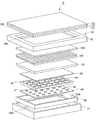
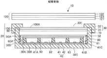
以下、本発明の実施形態に係るLEDバックライト装置およびLED画像表示装置について、図面を参照しながら説明する。本明細書において、「LED」とは、発光ダイオードを意味するものである。また、「シート」、「フィルム」、「板」等の用語は、呼称の違いのみに基づいて、互いから区別されるものではない。したがって、例えば、「シート」は、フィルムや板とも呼ばれるような部材も含む意味で用いられる。図1は本実施形態に係るLED画像表示装置の分解斜視図であり、図2は本実施形態に係るLED画像表示装置の概略構成図であり、図3は本実施形態に係るLEDバックライト装置の一部の拡大断面図である。図4は図1に示される第1の光学シートの平面図であり、図5は実施形態に係る他の第1の光学シートの平面図であり、図6は図1に示される第1のスペーサの平面図であり、図7は図1に示される第1の光学シートと第1のスペーサとの配置関係を示す平面図である。図8は実施形態に係る他の第1のスペーサの平面図であり、図9は図1に示される第1のスペーサと第2のスペーサとの配置関係を示す平面図であり、図10は図1に示されるレンズシートの断面図である。 Hereinafter, an LED backlight device and an LED image display device according to an embodiment of the present invention will be described with reference to the drawings. In this specification, “LED” means a light emitting diode. Further, terms such as “sheet”, “film”, and “plate” are not distinguished from each other based only on the difference in designation. Therefore, for example, “sheet” is used to include a member called a film or a plate. FIG. 1 is an exploded perspective view of an LED image display device according to the present embodiment, FIG. 2 is a schematic configuration diagram of the LED image display device according to the present embodiment, and FIG. 3 is an LED backlight device according to the present embodiment. FIG. 4 is a plan view of the first optical sheet shown in FIG. 1, FIG. 5 is a plan view of another first optical sheet according to the embodiment, and FIG. 6 is a plan view of the first optical sheet shown in FIG. FIG. 7 is a plan view showing the arrangement relationship between the first optical sheet and the first spacer shown in FIG. FIG. 8 is a plan view of another first spacer according to the embodiment, FIG. 9 is a plan view showing the positional relationship between the first spacer and the second spacer shown in FIG. 1, and FIG. It is sectional drawing of the lens sheet shown by FIG.
<<<<LED画像表示装置>>>>
図1および図2に示されるLED画像表示装置10は、直下型のLEDバックライト装置20と、LEDバックライト装置20よりも観察者側に配置された表示パネル120とを備えている。
<<<<< LED image display device >>>>
The LED
<<<表示パネル>>>
図1および図2に示される表示パネル120は、液晶表示パネルであり、入光側に配置された偏光板121と、出光側に配置された偏光板112と、偏光板121と偏光板122との間に配置された液晶セル123とを備えている。偏光板121、122および液晶セル123としては、公知の偏光板および液晶セルを用いることができる。
<<< Display Panel >>>
The
<<<LEDバックライト装置>>>
図1または図2に示されるLEDバックライト装置20は、筐体30と、LED実装基板40と、第1の光学シート50と、第1のスペーサ60と、第2の光学シート70と、第2のスペーサ80とを備えている。また、LEDバックライト装置20は、その他、第2の光学シート70に積層されたレンズシート90および反射型偏光分離シート100を備えている。なお、LEDバックライト装置20は、LED実装基板40、第1の光学シート50、第1のスペーサ60、第2の光学シート70、および第2のスペーサ80を備えていればよく、筐体30、レンズシート90、または反射型偏光分離シート100を備えていなくともよい。
<<< LED backlight device >>>
The
車載用LEDバックライト装置は車両内の非常に狭い空間に配置されるので、一般のLEDバックライト装置よりも薄型化を図ることが望まれている。このため、LEDバックライト装置20の総厚は、薄型化を図る観点から、15mm以下となっていることが好ましく、10mm以下となっていることがより好ましい。「LEDバックライト装置」の総厚とは、図2に示される筐体30の外底面30Cから反射型偏光分離シート100の表面100Aまでの距離を意味するものとする。
Since the vehicle-mounted LED backlight device is disposed in a very narrow space in the vehicle, it is desired to make the LED backlight device thinner than a general LED backlight device. For this reason, the total thickness of the
<<筐体>>
筐体30は、LED実装基板40等を収容する収容空間30Aを備えている。筐体30は、図2または図3に示されるように、内側の底面である内底面30B、外側の底面である外底面30C、および内底面30Bから立ち上がる内側の側面である内側面30Dを有している。また、筐体30は、図2に示されるように、LED素子42からの光を筐体30から出射させるための開口部30Eを有している。開口部30Eは、内底面30Bに対向する位置に設けられていることが好ましい。開口部30Eの形状は、特に限定されず、例えば、矩形状または円形状が挙げられる。
<< Case >>
The
図1および図2に示される筐体30は、収容空間30Aを有する筐体本体31と、筐体本体31の収容空間30Aを覆い、かつ開口部30Eを有する枠状の蓋体32とを備えている。筐体30においては、筐体30の内底面30Bは筐体本体31の内底面となっており、筐体30の内側面30Dは筐体本体31の内側面となっている。
The
筐体30(筐体本体31および蓋体32)は、金属から構成されていることが好ましい。特に、筐体本体31を金属から構成することによって、筐体本体31が放熱構造体としても機能するので、LED素子42からの熱を効率良く、放熱させることができる。金属としては、特に限定されないが、例えば、アルミニウム等が挙げられる。LEDバックライト装置20を曲げる場合、筐体30が曲げ可能な場合には、筐体30を筐体30内に収容される収容物とともに曲げてもよいが、筐体30としては予め曲げておいたものを使用することが好ましい。
The casing 30 (the casing
<<LED実装基板>>
LED実装基板40は、フレキシブル配線基板41と、フレキシブル配線基板41の一方の面(以下、この面を「表面」と称する。)41Aに実装された複数のLED素子42とを備えている。「フレキシブル」とは、柔軟性があることを意味しており、「フレキシブル配線基板」とは、一般的に可撓性があり、曲げることが可能な配線基板を意味するものとする。本明細書における「可撓性」とは、少なくとも曲率半径が1mとなるように曲がることを意味する。フレキシブル配線基板は、曲率半径が、好ましくは50cm、より好ましくは30cm、更に好ましくは10cm、特に好ましくは5cmとなるように曲がる。
<< LED mounting board >>
The
LED実装基板40は、図2および図3に示されるように、配線基板41におけるLED素子42が実装された表面41Aとは反対側の面(以下、この面を「裏面」と称する)41Bが筐体30の内底面30B側に位置するように筐体30内に配置されている。
2 and 3, the
<フレキシブル配線基板>
フレキシブル配線基板41においては、図3に示されるように、第1の光学フィルム50に向けて、樹脂フィルム43と、金属配線部44と、絶縁性保護膜45と、反射層46とがこの順で積層されている。ただし、フレキシブル配線基板41は、絶縁性保護膜45や反射層46を備えていなくともよい。また、金属配線部44は、樹脂フィルム43に対し、接着層47を介したドライラミネート法によって接着されていることが好ましい。さらに、金属配線部44は、LED素子42とはんだ層48を介して電気的に接続されている。
<Flexible wiring board>
In the
(樹脂フィルム)
樹脂フィルム43は、可撓性を有している。樹脂フィルム43は、曲率半径が、好ましくは50cm、より好ましくは30cm、更に好ましくは10cm、特に好ましくは5cmとなるように曲がるフィルムである。
(Resin film)
The
樹脂フィルム43は、公知の熱可塑性樹脂を用いて形成することができる。樹脂フィルム43の材料として用いる熱可塑性樹脂には耐熱性および絶縁性が高いものであるが好ましい。このような樹脂として、耐熱性と加熱時の寸法安定性、機械的強度、および耐久性に優れるポリイミド(PI)や、ポリエチレンナフタレート(PEN)を用いることができる。これらの中でも、アニール処理等の耐熱性向上処理を施すことによって耐熱性と寸法安定性を向上させたポリエチレンナフタレート(PEN)を好ましく用いることもできる。また、難燃性の無機フィラー等の添加によって難燃性を向上させたポリエチレンテレフタレート(PET)も樹脂フィルムを形成するための樹脂として選択することができる。
The
樹脂フィルム43を形成する熱可塑性樹脂は、熱収縮開始温度が100℃以上のもの、または、上記のアニール処理等によって、同温度が100℃以上となるように耐熱性を向上させたものを用いることが好ましい。本明細書における「熱収縮開始温度」とは、熱機械分析(TMA)装置に測定対象の熱可塑性樹脂からなるサンプルフィルムをセットし、荷重1gをかけて、昇温速度2℃/分で120℃まで昇温し、その時の収縮量(%表示)を測定し、このデータを出力して温度と収縮量を記録したグラフから、収縮によって、0%のベースラインから離れる温度を読みとり、その温度を熱収縮開始温度としたものである。なお、熱収縮開始温度は、3回測定して得られた値の算術平均値とする。
As the thermoplastic resin for forming the
通常LED素子からの熱によりLED素子周辺部は90℃程度の温度に達する場合がある。この観点から、樹脂フィルム43を形成する熱可塑性樹脂は、上記温度以上の耐熱性を有するものであることが好ましい。
Usually, the LED element periphery may reach a temperature of about 90 ° C. due to heat from the LED element. From this viewpoint, it is preferable that the thermoplastic resin forming the
樹脂フィルム43には、フレキシブル配線基板41に必要な絶縁性を付与し得るだけの高い絶縁性を有する樹脂であることが求められる。このため、樹脂フィルム43は、その体積固有抵抗率が1014Ω・cm以上であることが好ましく、1018Ω・cm以上であることがより好ましい。体積固有抵抗率は、JIS C2151:2006に準拠した方法で測定することができる。体積固有抵抗率は、ランダムに10箇所測定し、測定した10箇所の体積固有抵抗率の算術平均値とする。
The
樹脂フィルム43の厚みは、特に限定されないが、放熱経路としてボトルネックとはならないこと、耐熱性および絶縁性を有するものであること、ならびに、製造コストのバランスとの観点から、概ね10μm以上500μm以下であることが好ましい。また、ロール・トゥ・ロール方式による製造を行う場合の生産性を良好に維持する観点からも上記厚さ範囲であることが好ましい。樹脂フィルム43の厚みは、厚み測定装置(製品名「デジマチックインジケーターIDF−130」、ミツトヨ社製)を用いて任意の10箇所の厚さを測定し、その平均値を算出することにより求めるものとする。樹脂フィルム43の厚みの下限は、50μm以上であることが好ましく、樹脂フィルム43の厚みの上限は、250μm以下であることが好ましい。
The thickness of the
(金属配線部)
金属配線部44は、樹脂フィルム43よりLED素子42側に設けられ、かつLED素子42と電気的に接続されている。金属配線部44は、金属箔等をパターニングすることによって形成することができる。
(Metal wiring part)
The
金属配線部44を構成する金属の熱伝導率λは200W/(m・K)以上500W/(m・K)以下が好ましい。熱伝導率λは、例えば、熱伝導率計(製品名「QTM−500」、京都電子工業社製)を用いて測定することができる。熱伝導率λは、3回測定して得られた値の算術平均値とする。上記熱伝導率の下限は、300W/(m・K)以上であることがより好ましく、上限は500W/(m・K)以下であることが好ましい。銅の場合、熱伝導率λは403W/(m・K)である。
The metal constituting the
金属配線部44を構成する金属の電気抵抗率Rは3.00×10⁻⁸Ωm以下が好ましく、2.50×10⁻⁸Ωm以下がより好ましい。電気抵抗率Rは、エレクトロメータ(製品名「6517B型エレクトロメータ」、ケースレー社製)を用いて測定することができる。電気抵抗率Rは、3回測定して得られた値の算術平均値とする。銅の場合、電気抵抗率Rは1.55×10⁻⁸Ωmとなる。
The metal resistivity R constituting the
例えば、金属配線部44を銅箔で形成した場合、放熱性と電気伝導性を高い水準で両立させることができる。より具体的には、LED素子からの放熱性が安定し、電気抵抗の増加を防げるので、LED間の発光バラツキが小さくなってLEDの安定した発光が可能となる。また、LED素子の寿命も延長される。更に、熱による樹脂フィルム等の周辺部材の劣化も防止できるので、LEDバックライトを組み込んだLED画像表示装置の製品寿命も延長できる。
For example, when the
金属配線部44を形成する金属の例としては、上記の銅の他、アルミニウム、金、銀等の金属を挙げることができる。
Examples of the metal forming the
金属配線部44は電解銅箔であり、また、金属配線部44における樹脂フィルム43側の面の十点平均粗さRzが1.0μm以上10.0μm以下であることがより好ましい。十点平均粗さRzを上記範囲内とすることで、特に金属配線部44における樹脂フィルム43側の面の表面積を増大させることができ、放熱性を更に高めることができる。また、この面が凹凸面となっているので、樹脂フィルム43との密着性をより向上でき、これによっても放熱性を向上できる。このような十点平均粗さRzを有する電解銅箔の面としては、電解銅箔の粗面側(マット面側)を好適に用いることができる。十点平均粗さRzは、JIS B0601:1999に準拠して、例えば、表面粗さ測定器(製品名「SE−3400」、小坂研究所製社製)を用いて測定することができる。十点平均粗さRzは、3回測定して得られた値の算術平均値とする。
The
金属配線部44の配置は、LED素子42の導通可能な配置、好ましくはLED素子42をマトリックス状に配置できるものであれば、特定の配置に限定されない。ただし、フレキシブル配線基板41においては、樹脂フィルム43の一方の表面の好ましくは80%以上、より好ましくは90%、最も好ましくは95%以上の範囲が、この金属配線部44によって被覆されていることが好ましい。これにより、LED素子42を高密度で配置することができるとともに、発生する過剰な熱を、十分に金属配線部44を通じて速やかに拡散させ、樹脂フィルム43を経由させて外部へ放熱させることができるので、優れた放熱性を有するLEDバックライト装置20を得ることができる。
The arrangement of the
金属配線部44の厚みは、フレキシブル配線基板41に要求される耐電流の大きさ等に応じて適宜設定すればよく、特に限定されないが、一例として10μm以上50μm以下としてもよい。放熱性向上の観点から、金属配線部44の厚みは、10μm以上であることが好ましい。また、金属配線部の厚さが10μm未満であると、樹脂フィルム43の熱収縮の影響が大きく、はんだリフロー処理時に処理後の反りが大きくなりやすいため、この観点からも金属配線部44の厚さは10μm以上であることが好ましい。一方、金属配線部の厚さが、50μm以下であることによって、配線基板の十分なフレキシブル性を維持することができ、重量増大によるハンドリング性の低下等も防止できる。金属配線部44の厚さは、樹脂フィルム43と同様の方法によって測定することができる。
The thickness of the
(絶縁性保護膜)
絶縁性保護膜45は、主としてフレキシブル配線基板41の耐マイグレーション特性を向上させるものである。絶縁性保護膜45は、金属配線部44の表面のうちLED素子42を実装するための接続部分を除く全面、および樹脂フィルム43の表面のうち金属配線部44の非形成部分の概ね全面を覆う態様で形成されている。
(Insulating protective film)
The insulating
絶縁性保護膜45は、熱硬化性樹脂を含む熱硬化性樹脂組成物の硬化物から構成されていることが好ましい。熱硬化性樹脂組成物としては、熱硬化温度が100℃以下程度のものであれば、公知の熱硬化性樹脂組成物を適宜好ましく用いることができる。具体的には、ポリエステル系樹脂、エポキシ系樹脂、エポキシ系およびフェノール系樹脂、エポキシアクリレート樹脂、シリコーン系樹脂等をそれぞれベース樹脂とする熱硬化性樹脂組成物を好ましく用いることができる。また、これらのうちでも、ポリエステル系樹脂を含む熱硬化性樹脂組成物は、可撓性に優れる点から、絶縁性保護膜45を形成するための材料として特に好ましい。
The insulating
絶縁性保護膜45を形成するための熱硬化性樹脂組成物は、例えば、二酸化チタン等の無機白色顔料を更に含有する白色の熱硬化性樹脂組成物であってもよい。絶縁性保護膜45を白色化することで、意匠性の向上を図ることができる。また、反射層の機能を絶縁性保護膜45に付与することもできる。
The thermosetting resin composition for forming the insulating
絶縁性の熱硬化性樹脂組成物を用いた絶縁性保護膜45の形成は、スクリーン印刷等の公知の方法によって行うことができる。
Formation of the insulating
絶縁性保護膜45の膜厚は、10μm以上100μm以下であることが好ましい。絶縁性保護膜45の膜厚が、10μm未満であると、絶縁性が低下するおそれがあり、また100μmを超えると、絶縁性保護層をスクリーン印刷によって形成する際の滲みや熱硬化時の収縮による配線基板の反り等が顕著に生じるおそれがある。絶縁性保護膜45の膜厚は、走査型電子顕微鏡(SEM)を用いて、絶縁性保護膜45の断面を撮影し、その断面の画像において絶縁性保護膜45の膜厚を20箇所測定し、その20箇所の膜厚の算術平均値とする。
The thickness of the insulating
(反射層)
反射層46は、主として波長380nm以上780nm以下の可視光波長域の光に対して高い反射性を有するものである。反射層46は、LEDバックライト装置20の発光能力の向上を目的として、フレキシブル配線基板41の表面41Aに、LED素子実装領域を除く領域を覆って積層されている。なお、この実施形態においては、反射層46は、平面視において、LED素子42を囲い、かつ、絶縁性保護膜45のLED素子実装領域によって除かれた領域の内周縁部が露出するように絶縁性保護膜45上に積層されている。また、これに限らず、例えば、絶縁性保護膜45のLED素子実装領域によって除かれた領域の内周縁部が露出せず、絶縁性保護膜45と反射層46との両方の内周縁部が一致して同一形状をなすように積層されていてもよい。
(Reflective layer)
The
反射層46は、LED素子42からの光を反射し、所定の方向へ導くための反射面を持つ部材であれば、特に限定されないが、発泡タイプの白色ポリエステル、白色ポリエチレン樹脂、銀蒸着ポリエステル等を、最終製品の用途とその要求スペック等に応じて適宜用いることができる。
The
反射層46の膜厚は、50μm以上1mm以下であることが好ましい。反射層46の膜厚が、50μm未満であると、所望の反射率が得られないおそれがあり、また反射層が薄すぎるので、所定の位置にセッティングしにくくなり、また1mmを超えると、高コストとなるとともに、LEDバックライト装置の薄型化を達成できないおそれがある。反射層46の膜厚は、絶縁性保護膜45の膜厚と同様の方法によって測定するものとすることができる。
The thickness of the
(接着層)
接着層47としては、公知の樹脂系接着剤を適宜用いることができる。それらの樹脂系接着剤のうち、ウレタン系、ポリカーボネート系、又はエポキシ系の接着剤等を特に好ましく用いることができる。この接着層47は、金属配線部44のエッチング処理後に樹脂フィルム43上に残存している。
(Adhesive layer)
As the
(はんだ層)
はんだ層48は、金属配線部44とLED素子42とを電気的および機械的に接合するためものである。このはんだ層48による接合方法としては、大きく分けて、リフロー方式あるはレーザー方式があるが、このいずれかによって行うことができる。
(Solder layer)
The
金属配線部とLED素子とをはんだによって接合する際、樹脂フィルムおよび金属配線部には多大な熱が加えられるので、樹脂フィルムと金属配線部の線膨張係数の違いから、樹脂フィルムおよび金属配線部からなるフレキシブル配線基板に反りが発生するおそれがある。このような反りを防ぐために、樹脂フィルム43における金属配線部44側の面とは反対側の面に金属箔を設けることが好ましい。また、このような金属箔を設けることにより、点灯時のLED実装基板40の熱をより筐体本体31に放熱させることもできる。
When joining the metal wiring part and the LED element with solder, a great amount of heat is applied to the resin film and the metal wiring part. Therefore, the resin film and the metal wiring part are affected by the difference in coefficient of linear expansion between the resin film and the metal wiring part. There exists a possibility that curvature may generate | occur | produce in the flexible wiring board which consists of. In order to prevent such warpage, it is preferable to provide a metal foil on the surface of the
<<LED素子>>
LED素子42は、P型半導体とN型半導体が接合されたPN接合部での発光を利用した発光素子である。LED素子としては、P型電極、N型電極を素子上面、下面に設けた構造と、素子片面にP型、N型電極の双方が設けられた構造が知られているが、いずれの構造のLED素子も、LEDバックライト装置20に用いることができる。ただし、上記のうち素子片面にP型、N型電極の双方が設けられた構造のLED素子を特に好ましく用いることができる。
<< LED element >>
The
LED素子42は、フレキシブル配線基板41上にマトリクス状に配置されている。本明細書における「マトリクス状」とは、行列状に二次元配列されている状態を意味するものとする。本実施形態においては、LED素子42はマトリクス状に配置されているが、LED素子の配置状態は、特に限定されず、例えば、LED素子は千鳥状に配置されていてもよい。LED素子42はフレキシブル配線基板41上に複数個実装されている。フレキシブル配線基板41に実装されるLED素子42の個数は、複数個であれば、特に限定されない。LED素子42の配置密度は、0.02個/cm2以上2.0個/cm2以下であることが好ましく、0.1個/cm2以上1.5個/cm2以下であることがより好ましい。
The
<<第1の光学シート>>
第1の光学シート50は、光学的な機能を有するシートである。第1の光学シートとしては、例えば、光透過反射シート等が挙げられる。図1および図2に示される第1の光学シート50は、光透過反射シートとなっている。光透過反射シートは、光を透過させる透過部と光を反射させる反射部を有し、ある部分では光を透過させ、他の部分では光を反射させることで、LED素子からの光を平面内に拡散させて、輝度の面内均一性を向上させる機能を有するものである。
<< first optical sheet >>
The first
第1の光学シート50は、LED実装基板40における複数のLED素子42と対向するように配置されている、また、第1の光学シート50は、第1のスペーサ60によってLED実装基板40に対して離間している。第1の光学シート50は、配線基板41と略平行に配置されている。
The first
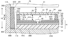
図3に示されるフレキシブル配線基板41の表面41Aから第1の光学シート50までの距離d1は0.6mm以上6mm以下となっている。本明細書における「配線基板の表面から第1の光学シートまでの距離」とは、フレキシブル配線基板41のように絶縁性保護層上に反射層を備えており、反射層の表面が配線基板の表面となっている場合には、反射層の表面から第1の光学シートにおける配線基板側の面までの距離を意味し、またフレキシブル配線基板の絶縁性保護層が反射層の機能を兼ね備えており、絶縁性保護層の表面がフレキシブル配線基板の表面となっている場合には、絶縁性保護層の表面から第1の光学シートにおける配線基板側の面までの距離を意味するものとする。また、第1の光学シートにおけるフレキシブル配線基板側の面とは、第1の光学シートにおける配線基板側の面が樹脂フィルムの面のみから構成されている場合には、樹脂フィルムにおけるフレキシブル配線基板側の面であるが、第1の光学シート50のように、樹脂フィルム54よりもフレキシブル配線基板41側に反射層55が形成されている場合には、反射層55におけるフレキシブル配線基板41側の面とする。
The distance d1 from the
第1の光学シート50の厚みは、25μm以上1mm以下であることが好ましい。光透過反射シートの厚みが、25μm未満であると、所望の反射率が得られないおそれがあり、また1mmを超えると、LEDバックライト装置の薄型化が図れないおそれがある。第1の光学シート50の厚さは、後述する反射部53の厚みとし、厚さ測定装置(製品名「デジマチックインジケーターIDF−130」、ミツトヨ社製)を用いて任意の10箇所の厚さを測定し、その平均値を算出することにより求めることができる。第1の光学シート50は、図4に示されるように、平面視において複数に分割された区画領域51を備えている。
The thickness of the first
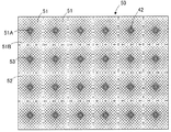
<区画領域>
区画領域51は、LED素子42の個数に合わせて分割されていることが好ましい。図4においては、LED素子(縦4個×横6個=24個)に対応して、縦4個×横6個=24個の区画領域51が形成されている。なお、図4においては点線で境界線が記載されているが、実際には境界線が形成されていることはなく、境界線は仮想線であり、区画領域51も仮想の領域である。
<Division area>
The
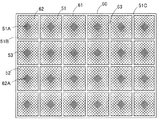
各区画領域51は、図4に示されるようにLED素子42からの光の一部を透過する複数の透過部52と、LED素子42からの光の一部を反射する複数の反射部53とで構成されている。透過部52および反射部53は、所定のパターンで構成されている。各区画領域におけるLED素子に対応する部分は最も多くの光が入射する部分となるので、この部分から光が透過すると、この部分の輝度が区画領域の他の部分の輝度よりも高くなってしまい、輝度の面内均一性が低下するおそれがある。このため、各区画領域51におけるLED素子42に対応する部分は反射部53から構成されていることが好ましい。なお、図3においては、形式的に、透過部52を白色で表しており、反射部53を灰色で表している。また、各区画領域51における透過部52および反射部53のパターンは同じとなっているが、必ずしも同じである必要はなく、区画領域によって異なるパターンであってもよい。透過部52および反射部53は、マス目状のパターンであってもよい。
As shown in FIG. 4, each
第1の光学シート50は、図4に示されるように、各区画領域51の中央部51Aが各LED素子42と対応する領域となるように配置されているので、外縁部51Bよりも中央部51Aに入射する光量は多くなる。このため、各区画領域51においては、透過部52の面積割合である開口率が、中央部51Aから外縁部51Bに向けて漸増していることが好ましい。各区画領域51における開口率を、中央部51Aから外縁部51Bに向けて漸増させることにより、十分な光量を確保した上で、発光面上における輝度の均一性をより向上させることができる。本明細書における「開口率」とは、一の区画領域を、25〜100等分程度の適当な割合で当分する等面積の正方形のマス目状に区切った際に、それぞれのマス目における透過部の面積比率のことを意味する。一の区画領域におけるこの等面積のマス目の規定の仕方は任意であるが、例えば、各マス目内に存在する透過部52の個数が概ね等数となるように設定することが望ましい。また、「開口率」は、一の区画領域の中心点を中心とする同心円を中央領域から中央領域の外側に位置する外側領域に向けて等間隔で複数規定し、各同心円の円周と円周の間の各領域内における透過部の面積比率を上記同様にして算出することによって求めたものであってもよい。この算出方法によれば、矩形の開口部が格子状に配置された一般的な開口配置以外の区画領域についても、上記の「開口率」を定義することができる。なお、各区画領域51においては、開口率が中央部51Aから外縁部51Bに向けて漸増していればよく、例えば中央部や外縁部近傍の限定された一部範囲において開口率が一定である領域が存在していてもよい。
As shown in FIG. 4, the first
各区画領域51の中央部51Aにおいては、面積比が主として反射部>透過部となっていることが好ましく、輝度の面内均一性を向上させる観点から、各区画領域51の中央部51Aは、反射部53のみから構成することがより好ましい。また、各区画領域51の外縁部51Bにおいては、面積比が主として透過部>反射部となっていることが好ましい。具体的には、外縁部51Bにおける透過部52の面積割合は、50%以上100%以下であることが好ましい。外縁部51Bにおける透過部52の面積割合の下限は、60%以上であることがより好ましく、70%以上であることが好ましい。なお、外縁部51Bでは反射部53を島状に形成することによって、理論的には透過部の面積割合を100%にすることもできる。このことは、従来の打ち抜き開口方式の光透過反射シートではなし得ない構成である。このように、第1の光学シート50の透過部52および反射部53を印刷方法によりパターン形成する場合には、パターニングのフレキシビリティを拡大させることができる。
In the
第1の光学シート50は、図3に示されるように、樹脂フィルム54と、樹脂フィルム54の少なくとも一方の面上の一部に積層された反射層55とで構成される。反射層55は、スクリーン印刷等によって形成することが可能である。この場合、第1の光学シート50のうち、反射層55が存在する領域が反射部53となり、反射層55が存在しない領域が透過部52となる。
As shown in FIG. 3, the first
<透過部>
透過部52は、樹脂フィルム54の両面のいずれにも反射層55が形成されてない領域であって、図3における樹脂フィルム54の両面が露出している領域である。樹脂フィルム54としては、従来公知の透明フィルムが好ましく用いられ、好ましくは全光線透過率が85%以上であることが好ましい。全光線透過率は、JIS K−7361:1997に準拠して、ヘイズメーター(製品名「HM−150」、村上色彩技術研究所製)を用いて、測定することができる。全光線透過率は、3回測定して得られた値の算術平均値とする。
<Transmission part>
The
樹脂フィルム54としては、例えばポリエチレンテレフタレート(PET)やポリエチレンナフタレート(PEN)が挙げられる。樹脂フィルム54の厚さは、12μm以上1mm(1000μm)以下であることが好ましい。樹脂フィルム54の厚さは、樹脂フィルム43の厚みと同様の方法によって測定することができる。
Examples of the
<反射部>
反射部53は、図3における第1の光学シート50における反射層55が存在する領域である。図3に示される反射部53は、樹脂フィルム54のLED素子42側の面に形成されているが、これに限らず、LED素子42の側の面とは反対側の面に形成されていてもよく、また、樹脂フィルム54の両面に形成されていてもよい。反射層55の膜厚は、20μm以上200μm以下であることが好ましい。反射層55の膜厚は、絶縁性保護膜45の膜厚と同様の方法によって測定することができる。
<Reflecting part>
The
反射部53においては、波長420nm以上780nm以下の可視光波長領域で少なくとも80%以上の反射率を有することが好ましい。第1の光学シート50における反射部53のように狭小な範囲に形成されている反射部の反射率は、顕微分光測定機(製品名「USPM−RU III」、オリンパス社製)を用いることより、正確に測定することができる。反射率の値は、硫酸バリウムを標準板とし、標準板を100%とした相対反射率を測定した値とする。なお、反射率は、3回測定して得られた値の算術平均値とする。
The reflecting
反射層55は、酸化チタン等の白色顔料を含む熱硬化性樹脂組成物の硬化物から構成することが可能である。反射層55中の白色顔料の含有量は、反射層中に10質量%以上85質量%以下であることが好ましい。
The
反射層55を構成する熱硬化性樹脂組成物中の熱硬化性樹脂としては、従来公知のウレタン樹脂とイソシアネート化合物との組み合わせ、エポキシ樹脂とポリアミンや酸無水物との組み合わせ、シリコーン樹脂と架橋剤との組み合わせのような、主剤と硬化剤とを含む2成分型の熱硬化性樹脂や、更に、アミン、イミダゾール、リン系等の硬化促進剤を含有する3成分型の熱硬化性樹脂が挙げられる。具体的には、熱硬化性樹脂としては、特開2014−129549に記載されているシリコーン系の熱硬化性樹脂が挙げられる。反射層55は、上記熱硬化性樹脂組成物を、例えば、スクリーン印刷等の印刷法を用いて樹脂フィルム54の表面にパターン印刷することによって形成することができる。なお、上記の厚さや反射率は、反射層が樹脂フィルムの両面に形成されている場合には両面の厚さの合計厚さであり、両面に反射層を形成した場合の反射率である。
Examples of the thermosetting resin in the thermosetting resin composition constituting the
図3に示される第1の光学シート50は、上記したように、樹脂フィルム54と、樹脂フィルム54の少なくとも一方の面上の一部に積層された反射層55とで構成されているが、第1の光学シートは、図5に示されるように、例えば、発泡ポリエチレンテレフタレート(PET)等の光反射性シート134に光反射性シート134の厚み方向に貫通する複数の開口部135を形成した第1の光学シート130であってもよい。第1の光学シート130は、第1の光学シート50と同様に、区画領域131、透過部132、および反射部133を備えている。第1の光学シート130における区画領域131、透過部132、および反射部133は、第1の光学シート50における区画領域51、透過部52、および反射部53と同様であるので、ここでは説明を省略するものとする。なお、第1の光学シート130の各区画領域131においても、透過部132の面積割合である開口率が、区画領域131の中央部131Aから区画領域131の外縁部131Bに向けて漸増していることが好ましい。第1の光学シート130の場合、開口部135は、光を透過させる透過部132として機能し、第1の光学シート130における開口部135以外の部分が、光を反射させる反射部133として機能する。開口部135は、任意の形状(例えば、円形状や矩形状)を有し、また所定のパターンに沿って互いに連結しないように分散配置されている。開口部135は、プレス打ち抜き加工、或いは、彫刻刃による抜き加工等により形成することができる。プレス打ち抜き加工は、ランニングコストや生産性に優れるため、大量生産する場合に有効な製造方法である。
As described above, the first
<<第1のスペーサ>>
第1のスペーサ60は、LED実装基板40に対し第1の光学シート50を離間させるためのものである。また、第1のスペーサ60は、フレキシブル配線基板41の表面41Aから第1の光学シート50までの距離d1を0.6mm以上6mm以下に保持する機能を有している。
<< First spacer >>
The
第1のスペーサ60は、第1の樹脂から構成されている。本明細書における「樹脂から構成されている」とは、樹脂が主の構成成分となっていることを意味する。第1の樹脂の25℃でのヤング率は、1GPa以上5GPa以下であることが好ましい。第1のスペーサ60を構成する樹脂のヤング率が、1GPa未満であると、第1のスペーサにおいて、フレキシブル配線基板や第1の光学シートを固定するための強度が確保できないおそれがあり、また5GPaを超えると、LEDバックライト装置を曲面などへ設置する際に第1のスペーサを曲げることができないおそれがある。第1の樹脂のヤング率は、動的粘弾性測定装置(製品名「Rheogel-E4000」、ユービーエム社製)を用いて、25℃で引張り試験を行い、縦軸に応力、横軸にひずみをとった応力−ひずみ曲線の直線部の傾きから求めるものとする。なお、上記ヤング率は、3回測定して得られた値の算術平均値とする。第1のスペーサ60を構成する樹脂の25℃でのヤング率の下限は、2GPa以上であることがより好ましく、上限は4GPa以下であることがより好ましい。
The
第1の樹脂としては、後述するように第2の樹脂よりも大きいヤング率を有すれば、特に限定されないが、反射率を高めて、第1の光学シート50に光を導く観点から白色系樹脂が好ましい。第1の樹脂としては、ポリカーボネート樹脂、アクリロニトリル−ブタジエン−スチレン共重合樹脂(ABS樹脂)、アクリロニトリル−スチレン−アクリレート共重合樹脂(ASA樹脂)、アクリロニトリル−ブタジエン−スチレン共重合樹脂(AES樹脂)、ポリメチルメタクリレート樹脂(PMMA樹脂)、ポリアセタール樹脂、ポリ塩化ビニル樹脂、ポリエチレン樹脂、ポリプロピレン樹脂、ポリエチレンテレフタレート樹脂、またはこれらの樹脂を2種以上混合した混合物等が挙げられる。これらの中でも、耐熱性や成形性等の観点から、ポリカーボネート樹脂、ABS樹脂、ASA樹脂、AES樹脂、PMMA樹脂、ポリアセタール樹脂、またはこれらの樹脂を2種以上混合した混合物が好ましい。
The first resin is not particularly limited as long as it has a Young's modulus greater than that of the second resin, as will be described later. However, the first resin is white based on the viewpoint of increasing the reflectance and guiding light to the first
図3に示される第1のスペーサ60の高さh1は、0.5mm以上5mm以下であることが好ましい。第1のスペーサの高さが、0.5mm未満であると、LED素子と第1の光学シートの距離が短すぎるために、第1の光学シートの平面視において、第1の光学シートの各区画領域の中央部が外縁部よりも明るくなるおそれがあり、また5mmを越えると、LEDバックライト装置の薄型化が図れないおそれがある。本明細書における「第1のスペーサの高さ」とは、第1のスペーサにおけるフレキシブル配線基板側の面である底面に垂直な方向において、第1のスペーサの底面から第1のスペーサにおける底面と反対側の面である上面までの距離を意味するものとする。第1のスペーサ60の高さh1は、第1のスペーサ60の高さをランダムに10箇所測定した値の算術平均値とする。
The height h1 of the
第1のスペーサ60とフレキシブル配線基板41は固定されていることが好ましい。第1のスペーサ60とフレキシブル配線基板41の固定方法としては、特に限定されず、接着や機械的固定手段による固定が挙げられる。本明細書における「接着」とは、「粘着」を含む概念である。図3においては、第1のスペーサ60とフレキシブル配線基板41は、両面テープ111を介して固定されている。具体的には、第1のスペーサ60の底面60A(後述する枠部61および桟部63の底面)とフレキシブル配線基板41の反射層46が、両面テープ111を介して接着されることによって固定されている。第1のスペーサ60とフレキシブル配線基板41を固定することにより、LED素子42に対する第1のスペーサ60の位置ずれをより抑制できる。なお、第1のスペーサ60とフレキシブル配線基板41は、両面テープ111ではなく、接着剤や粘着剤を用いて固定されていてもよい。
It is preferable that the
第1のスペーサ60と第1の光学シート50は固定されていることが好ましい。第1のスペーサ60と第1の光学シート50の固定方法としては、特に限定されず、接着や機械的固定手段による固定が挙げられる。図3においては、第1のスペーサ60と第1の光学シート50は、両面テープ112を介して接着されることによって固定されている。具体的には、第1のスペーサ60の上面60B(後述する枠部61および桟部63の上面)と第1の光学シート50が、両面テープ112を介して接着されている。第1のスペーサ60と第1の光学シート50を固定することにより、第1のスペーサ60およびLED素子42に対する第1の光学シート50の位置ずれをより抑制できる。なお、第1のスペーサ60と第1の光学シート50は、両面テープ112ではなく、接着剤や粘着剤を用いて固定されていてもよい。
The
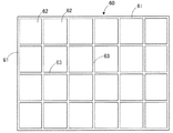
第1のスペーサ60は、図6に示されるように、枠部61と、枠部61よりも内側に位置した複数の開口部62と、開口部62間に位置した桟部63とを有している。
As shown in FIG. 6, the
図6に示される第1のスペーサ60は、格子状となっている。本明細書における「格子状」とは、第1のスペーサの平面視において、枠部および桟部によって形成された複数の開口部がマトリクス状に配置された構造を意味するものとする。第1のスペーサの平面視における開口部の形状としては、四角形状等の多角形状、楕円形状、円形状等が挙げられる。上記四角形状としては、正方形状、長方形状、菱形形状等が挙げられる。図6に示される第1のスペーサ60においては、枠部61および桟部63によって形成された四角形状の開口部62がマトリクス状に配置されている。また、枠部の角部および/または桟部の角部は、第1のスペーサの平面視において、曲線状となっていてもよい。
The
<枠部および桟部>
図6に示される枠部61は、平面視において四角形状となっているが、枠部の形状は、LED実装基板の形状等に合わせて、適宜変更することができる。枠部61は、ほぼフレキシブル配線基板41の大きさと同じ大きさになっている。
<Frame part and pier part>
The
桟部63は、開口部62間を仕切るものであり、枠部61と一体的に設けられている。本明細書における「一体的に設けられている」とは、枠部と桟部との間に境界が存在しない場合、すなわち枠部と桟部が一体形成されている場合のみならず、桟部が枠部に接合されている場合をも含む概念である。第1のスペーサ60においては、枠部61および桟部63が一体形成されている。枠部61および桟部63を一体形成することによって、繋ぎ目がない第1のスペーサを得ることができるので、第1のスペーサを複数の部材から構成するよりも、LEDバックライト装置の組立工程の簡素化、および振動試験における第1の光学シートの位置ずれリスクの低減を図ることができる。また、第1のスペーサには、繋ぎ目がないので、継ぎ目に入り込む光にもなく、光学的損失の低減を図ることができる。
The
桟部63は、図7に示されるように、区画領域51間の境界部51Cに対応する位置に配置されていることが好ましい。本明細書における「区画領域間の境界部」とは、透過部および反射部のパターンから区画領域間の境界と想定される領域を含む部分を意味するものとする。また桟部63は、枠部61と一体的に成型されていることが好ましい。なお、図7は、LED素子42側から第1のスペーサ60および第1の光学シート50を平面視した図である。
As shown in FIG. 7, the
図3に示されるように、枠部61および桟部63の少なくともいずれかの開口部62に面している側面61A、63Aが、フレキシブル配線基板41から第1の光学シート50に向けて開口部62の開口径が大きくなるように傾斜していることが好ましい。このような側面61A、63Aを有する枠部61および桟部63を形成することにより、LED素子62からの出射光を枠部61の側面61Aおよび桟部63の側面63Aで反射させて、第1の光学シート50に導くことができるので、LEDバックライト装置20からより効率良く光を出射させることができる。このような側面61A、63Aを有する枠部61および桟部63を備える第1のスペーサ60は、例えば、射出成型、切削や三次元プリンターによって得ることができる。側面61A、63Aは、第1のスペーサ60の高さ方向の断面において、曲線状となっていてもよいが、作製し易さの観点から、直線状となっていることが好ましい。
As shown in FIG. 3, the side surfaces 61 </ b> A and 63 </ b> A facing the
枠部および桟部の少なくともいずれかの第1の光学シート側の上面には、凸部が設けられていることが好ましい。第1のスペーサは、上記したように、射出成型、打ち抜き、切削、または三次元プリンターによって作製することが可能であるが、第1のスペーサに凸部を設ける場合には、これらの中でも、凸部の形成し易さの観点から、射出成型が好ましい。 It is preferable that a convex portion is provided on the upper surface of at least one of the frame portion and the crosspiece portion on the first optical sheet side. As described above, the first spacer can be manufactured by injection molding, punching, cutting, or a three-dimensional printer. However, when a convex portion is provided on the first spacer, among these, the convex From the viewpoint of easy formation of the part, injection molding is preferable.
第1のスペーサに凸部を設ける場合、第1の光学シートには孔部が設けられており、凸部が孔部に入り込んでいる。このような孔部および凸部を設けることによって、LED素子に対する第1の光学シートの位置合わせが容易となるとともに、振動試験を行った場合であっても、LED素子に対する第1の光学シートの位置ずれをより抑制することができる。 When providing a convex part in the 1st spacer, the hole is provided in the 1st optical sheet, and the convex part has entered the hole. By providing such a hole and a convex portion, the alignment of the first optical sheet with respect to the LED element is facilitated, and even when a vibration test is performed, the first optical sheet with respect to the LED element is not aligned. Misalignment can be further suppressed.
第1の光学シートとして、貫通する複数の開口部135を有する第1の光学シート130を用いる場合、開口部135のうち1以上の開口部135を上記孔部として利用してもよい。この場合、開口部135が貫通孔となっているので、孔部も貫通孔となっているが、開口部135と別に孔部を設ける場合には、孔部は貫通孔でなくともよい。本明細書における「孔部」とは、貫通孔のみならず、凹みのような貫通していない孔をも含む概念である。また、透過部として機能する開口部がない光学シートであっても、凸部を入り込ませる孔部を有する光学シートであれば、適用できる。
When using the 1st
上記凸部は、LED素子に対する透過部として機能する複数の開口部を有する第1の光学シートの位置を合わせ、およびこの第1の光学シートの位置ずれを抑制するためのものである。凸部は、上記孔部として機能する開口部に入り込んでいる。 The said convex part is for aligning the position of the 1st optical sheet which has several opening part which functions as a permeation | transmission part with respect to an LED element, and suppressing the position shift of this 1st optical sheet. The convex portion enters the opening that functions as the hole.
凸部の形状は、特に限定されないが、例えば、例えば、円錐形状、円錐台形状、角錐形状、角錐台形状、ドーム形状、不定形形状が挙げられる。 Although the shape of a convex part is not specifically limited, For example, a cone shape, a truncated cone shape, a pyramid shape, a truncated pyramid shape, a dome shape, and an indefinite shape are mentioned, for example.
凸部の高さは、第1の光学シートの光学性能に影響を与えない観点から、第1の光学シートの厚み以下(開口部の高さ以下)とすることが好ましい。また、第1の光学シートの位置ずれを抑制する観点からは、凸部の高さの下限は、第1の光学シートの厚みの1/4以上となっていることがより好ましい。 From the viewpoint of not affecting the optical performance of the first optical sheet, the height of the convex portion is preferably set to be equal to or less than the thickness of the first optical sheet (less than the height of the opening). Further, from the viewpoint of suppressing the positional deviation of the first optical sheet, it is more preferable that the lower limit of the height of the convex portion is ¼ or more of the thickness of the first optical sheet.
凸部の直径や幅は、特に限定されないが、第1の光学シートは、直径が異なる開口部が複数存在しているので、対象とする開口部よりも小さい開口部には入らないような直径であることが好ましい。 The diameter and width of the convex portion are not particularly limited, but the first optical sheet has a plurality of openings having different diameters, so that the diameter does not enter an opening smaller than the target opening. It is preferable that
凸部は、第1のスペーサ全体として1以上形成されていればよいが、第1の光学シートの位置ずれをより抑制する観点からは、複数個形成されていることが好ましい。さらに、第1の光学シートの位置ずれをさらに抑制する観点からは、第1のスペーサの平面視において、凸部によって四角形が描かれるように少なくとも4箇所に凸部が形成されていることが好ましい。 One or more protrusions may be formed as a whole of the first spacer, but a plurality of protrusions are preferably formed from the viewpoint of further suppressing the displacement of the first optical sheet. Furthermore, from the viewpoint of further suppressing the positional deviation of the first optical sheet, it is preferable that convex portions are formed at least at four places so that a quadrangle is drawn by the convex portions in a plan view of the first spacer. .
凸部を有する第1のスペーサは、射出成型によって作製することができる。また、凸部を別途作製し、枠部および桟部の少なくともいずれかに凸部を接着剤等や機械的固定によって固定することも可能であるが、接着剤等によって上記凸部を枠部および/または桟部に固定した場合には、凸部が枠部および/または桟部から剥がれるおそれがあるので、凸部と枠部および/または桟部とは射出成型によって一体的に形成することが好ましい。 The 1st spacer which has a convex part can be produced by injection molding. Further, it is possible to separately produce a convex part and fix the convex part to at least one of the frame part and the crosspiece part by an adhesive or the like or mechanical fixing. When fixed to the crosspiece, the convex portion may be peeled off from the frame portion and / or the crosspiece portion. Therefore, the convex portion and the frame portion and / or the crosspiece portion may be integrally formed by injection molding. preferable.
<開口部>
開口部62は、各LED素子42からの光を通過させるためのものであり、第1のスペーサ60の高さ方向に貫通している。開口部62は、第1のスペーサ60に複数設けられている。開口部62の個数は特に限定されないが、図6においては、LED素子42の個数(縦4個×横6個=24個)に対応して、縦4個×横6個=24個の開口部62が形成されている。
<Opening>
The
各開口部62は、各LED素子42からの光を通過させるものであるので、各開口部62は、第1のスペーサ60を平面視したとき、開口部62内にLED素子42が入る大きさとなっている。図7においては、1つの開口部62内に1個のLED素子62が配置されているが、1つの開口部内に複数個のLED素子が配置されていてもよい。
Since each
図6に示される開口部62は、全て同じ大きさとなっているが、開口部62は同じ大きさである必要はなく、異なる大きさであってもよい。
The
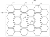
第1のスペーサ60は、格子状となっているが、第1のスペーサは、格子状となっていなくともよい。例えば、第1のスペーサは、枠部および桟部によって形成された開口部が千鳥状に配置されたものであってもよい。具体的には、第1のスペーサは、図8に示されるようにハニカム状となっていてもよい。図8に示されるハニカム状の第1のスペーサ140も、第1のスペーサ60と同様に、枠部141と、枠部141よりも内側に位置した複数の開口部142と、開口部142間に位置し、枠部141と一体的に設けられた桟部143とを有している。第1のスペーサ140は、ハニカム状となっている以外、第1のスペーサ60と同様となっているので、ここでは説明を省略するものとする。なお、LED素子42がマトリクス状に配置されたLED実装基板40を用いる場合には、格子状の第1のスペーサ60を用い、LED素子が千鳥状に配置されたLED実装基板を用いる場合には、ハニカム状の第1のスペーサ140を用いることができる。
Although the
<<第2の光学シート>>
第2の光学シート70は、光学的な機能を有するシートである。光学シートとしては、光学的な機能を有するシートであれば、特に限定されず、例えば、光拡散シート、レンズシート、または反射型偏光分離シート等が挙げられる。図1および図2に示される第2の光学シート70は、光拡散シートとなっている。光拡散シートである第2の光学シート70を配置することにより、第1の光学シート50を透過した光を第2の光学シート70でさらに拡散させることができ、輝度の面内均一性をさらに向上させることができる。なお、第2の光学シートが、レンズシートである場合には、レンズシート90は備えなくともよく、また第2の光学シートが、反射型偏光分離シートである場合には、反射型偏光分離シート100は備えなくともよい。また、第2の光学シートとして、レンズシートや反射型偏光分離シートを用いる場合には、レンズシート90や反射型偏光分離シート100と同様のものを用いることができる。
<< second optical sheet >>
The second
第2の光学シート70は、第1の光学シート50の光出射側に配置されている。第2の光学シート70は、第2のスペーサ80によって第1の光学シート50に対し離間している。第2の光学シート70は、第1の光学シート50と略平行に配置されている。
The second
図3に示される第1の光学シート50から第2の光学シート70までの距離d2は、0.5mm以上5mm以下であることが好ましい。第1の光学シート50から第2の光学シート70までの距離が、0.5mm未満であると、光拡散機能が十分に発揮されないおそれがあり、また5mmを超えると、LEDバックライト装置の薄型化が図れないおそれがある。本明細書における「第1の光学シートから第2の光学シートまでの距離」とは、第1の光学シートにおける第2の光学シート側の面から第2の光学シートにおける第1の光学シート側の面までの距離を意味するものとする。第1の光学シート50から第2の光学シート70までの距離は、この距離をランダムに10箇所測定した値の算術平均値とする。
The distance d2 from the first
フレキシブル配線基板41の表面41Aから第2の光学シート70までの距離(OD)は、LEDバックライト装置20の薄型化を図る観点から、1mm以上10mm以下となっていることが好ましい。本明細書における「フレキシブル配線基板の表面から第2の光学シートまでの距離」とは、フレキシブル配線基板の表面から第2の光学シートにおけるフレキシブル配線基板側の面までの距離を意味するものとする。配線基板41の表面41Aから第2の光学シート70までの距離は、この距離をランダムに10箇所測定した値の算術平均値とする。フレキシブル配線基板41の表面41Aから第2の光学シート70までの距離の上限は、5mm以下となっていることが好ましい。
From the viewpoint of reducing the thickness of the
第2の光学シート70の厚みは、第1の光学シート50の厚みよりも大きくなっていることが好ましい。第2の光学シート70の厚みが、第1の光学シート50の厚みより大きいことにより、第2の光学シート70は、第1の光学シート50よりも撓み難い。このため、第2の光学シート70は、枠状の第2のスペーサ80によって、第1の光学シート50と第2の光学シート70との間の距離を所定の距離に保持することができる。
The thickness of the second
第2の光学シート70の厚みは、0.3mm以上5mm以下であることが好ましい。第2の光学シート70の厚みが、0.3mm未満であると、光拡散効果が十分に得られないおそれがあるからであり、また厚みが、5mmを超えると、LEDバックライト装置の薄型化が図れないおそれがある。第2の光学シート70の厚みは、第1の光学シート50の厚さと同様の方法によって測定することができる。
The thickness of the second
第2の光学シート70は、樹脂から構成されていることが好ましい。第2の光学シート70は、ポリカーボネート樹脂やアクリル樹脂等からなる半透明の樹脂フィルムと、樹脂フィルムの一方の面側に形成された、光拡散機能を発揮するための、例えば、微小でランダムなレンズアレイ等を有するレンズ層とを備えている。
It is preferable that the 2nd
<<第2のスペーサ>>
第2のスペーサ80は、第1の光学シート50に対し第2の光学シート70を離間させるためのものである。また、第2のスペーサ80は、第1の光学シート50から第2の光学シート70までの距離d2を0.5mm以上5mm以下に保持するとともに、配線基板41の表面41Aから第2の光学シート70までの距離を1mm以上10mm以下に保持する機能を有している。
<< Second spacer >>
The
第2のスペーサ80は、第2の樹脂から構成されている。第2のスペーサ80を構成する第2の樹脂の25℃でのヤング率は、第1のスペーサ60を構成する第1の樹脂の25℃でのヤング率よりも小さくなっている。第2のスペーサ80を構成する第2の樹脂の25℃でのヤング率は、第1のスペーサ60を構成する第1の樹脂の25℃でのヤング率と同様の方法によって測定するものとする。
The
第1の樹脂のヤング率と第2の樹脂のヤング率との差(第1の樹脂のヤング率−第2の樹脂のヤング率)は、0.05GPa以上2GPa以下であることが好ましい。この差が、0.05GPa以上であれば、LEDバックライト装置20を曲面に設置する際に第2のスペーサ80を所望の曲率で曲げることができるので、第2のスペーサ80の破損をより抑制することができ、また2GPa以下であれば、第2のスペーサ80においても所望の強度を得ることができる。この差の下限は、0.1GPa以上であることがより好ましく、上限は1GPa以下であることがより好ましい。
The difference between the Young's modulus of the first resin and the Young's modulus of the second resin (Young's modulus of the first resin−Young's modulus of the second resin) is preferably 0.05 GPa or more and 2 GPa or less. If this difference is 0.05 GPa or more, the
第2の樹脂のヤング率は、0.5GPa以上4GPa以下であることが好ましい。第2の樹脂のヤング率が、0.5GPa未満であると、第2の光学シートを固定および支持するための所望の強度が得られないおそれがあり、また4GPaを超えると、LEDバックライト装置を曲面などへ設置する際に第2のスペーサを曲げることができないおそれがある。第2の樹脂のヤング率の下限は、1GPa以上であることがより好ましく、上限は3GPa以下であることがより好ましい。 The Young's modulus of the second resin is preferably 0.5 GPa or more and 4 GPa or less. If the Young's modulus of the second resin is less than 0.5 GPa, the desired strength for fixing and supporting the second optical sheet may not be obtained, and if it exceeds 4 GPa, the LED backlight device There is a possibility that the second spacer cannot be bent when the is installed on a curved surface or the like. The lower limit of the Young's modulus of the second resin is more preferably 1 GPa or more, and the upper limit is more preferably 3 GPa or less.
第2の樹脂の中でも、反射率を高めて、第2の光学シート70に光をより導く観点から白色系樹脂が好ましい。第2の樹脂としては、ポリカーボネート樹脂、アクリロニトリル−ブタジエン−スチレン共重合樹脂(ABS樹脂)、アクリロニトリル−スチレン−アクリレート共重合樹脂(ASA樹脂)、アクリロニトリル−ブタジエン−スチレン共重合樹脂(AES樹脂)、ポリメチルメタクリレート樹脂(PMMA樹脂)、ポリアセタール樹脂、ポリ塩化ビニル樹脂、ポリエチレン樹脂、ポリプロピレン樹脂、またはこれらの樹脂を2種以上混合した混合物等が挙げられる。これらの中でも、耐熱性や成形性等の観点から、ポリカーボネート樹脂、ABS樹脂、ASA樹脂、AES樹脂、ポリアセタール樹脂、ポリエチレン樹脂、ポリプロピレン樹脂、またはこれらの樹脂を2種以上混合した混合物が好ましい。
Among the second resins, a white resin is preferable from the viewpoint of increasing the reflectance and further guiding light to the second
図3に示される第2のスペーサ80の高さh2は、第1のスペーサ60の高さh1よりも大きくなっている。第2のスペーサ70の高さh2は、1mm以上10mm以下であることが好ましい。第2のスペーサの高さが、1mm未満であると、第1の光学シートと第2の光学シートとの距離が短すぎるために、第2の光学シートの平面視において、第1の光学シートの各区画領域の中央部に対応する部分が外縁部に対応する部分よりも明るくなるおそれがあり、また10mmを越えると、LEDバックライト装置の薄型化が図れないというおそれがある。本明細書における「第2のスペーサの高さ」とは、第2のスペーサにおける筐体の内底面側の面である底面に垂直な方向において、第2のスペーサの底面から第2のスペーサの上面までの距離を意味するものとする。第2のスペーサ80の高さh2は、第2のスペーサ80の高さをランダムに10箇所測定した値の算術平均値とする。
The height h2 of the
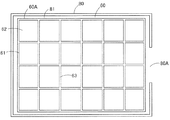
第2のスペーサ80は、図9に示されるように、枠状となっている。本明細書の「枠状」とは、切れ間なく1周繋がっている構成のみならず、概ね繋がっていれば途中で切れ間があってもよい。図9に示される第2のスペーサ80は、端子等との接続のために、切れ間80Aが設けられている。第2のスペーサ80は、1つの開口部81を有しており、第1の光学シート50の外周面50Aおよび第1のスペーサ60の外周面60Aを取り囲むように配置されている。第2のスペーサ80は、図2に示されるように、第1の光学シート50の外周面50Aおよび第1のスペーサ60の外周面60Aのみならず、フレキシブル配線基板41の外周面41Cを取り囲むように配置されている。すなわち、第2のスペーサ80の内側には、LED実装基板40、第1の光学シート50、および第1のスペーサ60が位置している。第2のスペーサ80が枠状になっていることにより、第1の光学シート50を透過して、第2のスペーサ80側に向かう光を第2のスペーサ80で反射させて、第2の光学シート70に導くことができる。また、第2のスペーサ80が枠状となっていることにより、第2のスペーサが複数の柱状体から構成されている場合よりも、第2の光学シート70との接触面積を増大させることができるので、LEDバックライト装置20の使用時において、第2のスペーサ80を介して第2の光学シート70の熱をより放熱させることができる。また、第2のスペーサ80が枠状となっていることにより、第2のスペーサが複数の柱状体から構成されている場合よりも、第2のスペーサ80と第2の光学シート70との接着面積を増大させることができるので、より第2の光学シート70が位置ずれしにくい。
As shown in FIG. 9, the
図3に示されるように、第2のスペーサ80の底面80Bは筐体30の内底面30Bに接していることが好ましい。本明細書における「第2のスペーサの底面が筐体の内底面と接している」とは、第2のスペーサの底面が筐体の内底面に直接接触している場合に限らず、第2のスペーサの底面と筐体の内底面との間に、両面テープ、粘着剤または接着剤等、熱伝導という観点でほぼ無視できる層が介在している場合をも含む概念である。図3においては、第2のスペーサ80の底面80Bと筐体30の内底面30Bとの間には、後述する両面テープ113が介在している。
As shown in FIG. 3, the
また、図3に示される第2のスペーサ80の外側の側面である外側面80Cは筐体30の内側面30Dに接している。本明細書における「第2のスペーサの外側面」とは、第2のスペーサの開口部を画定する内側面とは反対側の面を意味するものとする。また、本明細書における「第2のスペーサの外側面が筐体の内側面と接している」とは、第2のスペーサの外側面が筐体の内側面に直接接触している場合に限らず、第2のスペーサの外側面と筐体の内側面との間に、両面テープ、粘着剤または接着剤等、熱伝導という観点でほぼ無視できる層が介在している場合をも含む概念である。図3においては、第2のスペーサ80の外側面80Cは、筐体30の内側面30Dに直接接している。
Also, the
第2のスペーサ80と筐体30は、LED素子42に対する光学シート70の位置ずれをより抑制する観点から、固定されていることが好ましい。第2のスペーサ80と筐体30の固定方法としては、特に限定されず、接着や機械的固定手段による固定が挙げられる。図3においては、第2のスペーサ80の底面80Bと筐体30の内底面30Bが、両面テープ113を介して接着されることによって固定されている。ここで、第2のスペーサ80は、枠状となっているので、第2のスペーサが複数の柱状体から構成されている場合よりも、筐体30との接着面積を増大させることができるので、第2のスペーサ80を固定しやすい。なお、第2のスペーサ80と筐体30は、両面テープ113ではなく、接着剤や粘着剤を介して接着されていてもよい。
The
第2のスペーサ80と第2の光学シート70は、固定されていることが好ましい。第2のスペーサ80と第2の光学シート70の固定方法としては、特に限定されず、接着や機械的固定手段による固定が挙げられる。図3においては、第2のスペーサ80における底面80Bは反対側の上面80Dと第2の光学シート70が、両面テープ114を介して接着されることによって固定されている。第2のスペーサ80と第2の光学シート70を固定することにより、LED素子42に対する第2のスペーサ80の位置ずれをより抑制できる。なお、第2のスペーサ80と第2の光学シート70は、両面テープ114ではなく、接着剤や粘着剤を用いて固定されていてもよい。
The
図3に示されるように、第2のスペーサ80の内側の側面である内側面80Eは、筐体30の内底面30Bから第2の光学シート70に向けて開口部81の開口径が大きくなるように傾斜していることが好ましい。このような内側面80Eを有する第2のスペーサ80を形成することにより、第1の光学シート50からの出射光を第2のスペーサ80の内側面80Eで反射させて、第2の光学シート70に導くことができるので、LEDバックライト装置20からより効率良く光を出射させることができる。このような内側面80Dを有する第2のスペーサ80は、例えば、射出成型、打ち抜き、切削または三次元プリンターによって得ることができる。内側面80Eは、第2のスペーサ80の高さ方向の断面において、曲線状となっていてもよいが、作製し易さの観点から、直線状となっていることが好ましい。
As shown in FIG. 3, the
<<レンズシート>>
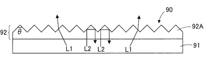
レンズシート90は、入射した光の進行方向を変化させて出光側から出射させる機能を有する。レンズシート90は、図10に示されるように、例えばL1のような入射角度が大きい光の進行方向を変化させて出光側から出射させて、正面方向の輝度を集中的に向上させる機能(集光機能)とともに、例えばL2のような入射角度が小さい光を反射させて、第2の光学シート80側に戻す機能(再帰反射機能)を有している。レンズシート90は、図10に示されるように、樹脂フィルム91と、樹脂フィルム91の一方の面に設けられたレンズ層92とを備えている。なお、レンズシート90は、レンズ層92が樹脂フィルム91よりも反射型偏光分離シート100側に位置するように配置されている。
<< Lens sheet >>
The
(樹脂フィルム)
樹脂フィルム91の構成材料としては、例えば、ポリエステル(例えば、ポリエチレンテレフタレート、ポリエチレンナフタレート)、セルローストリアセテート、セルロースジアセテート、セルロースアセテートブチレート、ポリアミド、ポリイミド、ポリエーテルスルフォン、ポリスルフォン、ポリプロピレン、ポリメチルペンテン、ポリ塩化ビニル、ポリビニルアセタール、ポリエーテルケトン、ポリメタクリル酸メチル、ポリカーボネート、又は、ポリウレタン等の熱可塑性樹脂が挙げられる。
(Resin film)
Examples of the constituent material of the
(レンズ層)
レンズ層92は、出光側に並べて配置された複数の単位レンズ92Aを備えている。単位レンズ92Aは、三角柱状であってもよいし、波状や例えば半球状のような椀状であってもよい。具体的には、単位レンズとしては、単位プリズム、単位シリンドリカルレンズ、単位マイクロレンズ等が挙げられる。なお、そのような単位レンズ形状を有するレンズシートとしては、プリズムシート、レンチキュラーレンズシート、マイクロレンズシート等が挙げられる。
(Lens layer)
The
単位レンズ92Aは、光の利用効率を向上させる観点から、80°以上100°以下の頂角θを有することが好ましく、約90°の頂角を有することがより好ましい。
The
<反射型偏光分離シート>
反射型偏光分離シート100は、レンズシート90から出射される光のうち、第1の直線偏光成分(例えば、P偏光)のみを透過し、かつ第1の直線偏光成分と直交する第2の直線偏光成分(例えば、S偏光)を吸収せずに反射する機能を有するものである。反射型偏光分離シート100で反射された第2の直線偏光成分は再度反射され、偏光が解消された状態(第1の直線偏光成分と第2の直線偏光成分とを両方含んだ状態)で、再度、反射型偏光分離シート100に入射する。
<Reflection-type polarized light separation sheet>
The reflection-type
反射型偏光分離シート100としては、3M社から入手可能な「DBEF」(登録商標)を用いることができる。また、「DBEF」以外にも、Shinwha Intertek社から入手可能な高輝度偏光シート「WRPS」やワイヤーグリッド偏光子等を、反射型偏光分離シート63として用いることができる。
As the reflective
第1のスペーサの外周面を取り囲むように枠状の第2のスペーサを配置した場合、第2のスペーサは第1のスペーサよりも外側にあるので、LEDバックライト装置を曲げた際には、第2のスペーサの変化量は、第1のスペーサの変化量よりも大きくなる。このため、LEDバックライト装置を曲げた場合には、第2のスペーサは、第1のスペーサよりも割れやすい。一方で、第1のスペーサおよび第2のスペーサをヤング率が低い樹脂から構成した場合には、LEDバックライト装置の剛性が低下してしまう。これに対し、本実施形態においては、第1のスペーサ60の外周面60Aを取り囲むように枠状の第2のスペーサ80を配置しているが、第2のスペーサ80を構成する第2の樹脂の25℃でのヤング率が、第1のスペーサ60を構成する第1の樹脂の25℃でのヤング率よりも小さくなっているので、第1のスペーサ60よりも第2のスペーサ80の方が、柔軟性が高くなっている。これにより、LEDバックライト装置20を曲げた場合であっても、第2のスペーサ80の割れを抑制することができるので、LEDバックライト装置の剛性の低下を抑制しつつ、曲げ可能なLEDバックライト装置20を提供することができる。
When the frame-shaped second spacer is disposed so as to surround the outer peripheral surface of the first spacer, the second spacer is located outside the first spacer. Therefore, when the LED backlight device is bent, The amount of change of the second spacer is larger than the amount of change of the first spacer. For this reason, when the LED backlight device is bent, the second spacer is easier to crack than the first spacer. On the other hand, when the first spacer and the second spacer are made of a resin having a low Young's modulus, the rigidity of the LED backlight device is lowered. On the other hand, in the present embodiment, the frame-shaped
上記したように、通常、配線基板と光学シートとの間には、配線基板に対し光学シートを離間させるためのスペーサとして、複数の柱状のスペーサを配置しているが、柱状のスペーサを用いると、LEDバックライト装置を曲げた場合に、配線基板と光学シートとの距離が変わるおそれがある。特に、光学シートが光透過反射シートである場合には、光透過反射シートは各区画領域に透過部および反射部のパターンを有しているので、配線基板と光透過反射シートとの距離が変わってしまうと、輝度の面内均一性が低下するおそれがある。このため、LEDバックライト装置を曲げた場合であっても、配線基板と光学シートの距離は所定の距離に保持することが望まれる。これに対し、第1のスペーサ60が、枠部61と、枠部61と一体的に設けられた桟部63とを備えているので、柱状のスペーサに比べて、第1の光学シート50との接触面積を増大させることができる。これにより、LEDバックライト装置20を曲げた場合であっても、フレキシブル配線基板41と第1の光学シート50との距離を所定の距離に保持することができる。また、第1のスペーサ60によって、LEDバックライト装置20を曲げた場合であっても、フレキシブル配線基板41と光透過反射シートである第1の光学シート50との距離を所定の距離に保持することができるので、輝度の面内均一性を向上させることができる。
As described above, usually, a plurality of columnar spacers are arranged between the wiring board and the optical sheet as spacers for separating the optical sheet from the wiring board. When the LED backlight device is bent, the distance between the wiring board and the optical sheet may change. In particular, when the optical sheet is a light-transmitting / reflecting sheet, the distance between the wiring board and the light-transmitting / reflecting sheet changes because the light-transmitting / reflecting sheet has patterns of transmitting portions and reflecting portions in each partition region. If this is the case, the in-plane uniformity of the brightness may be reduced. For this reason, even when the LED backlight device is bent, it is desirable to keep the distance between the wiring board and the optical sheet at a predetermined distance. On the other hand, since the
また、配線基板と光学シートの距離を所定の距離に保持するためのスペーサとして、複数の柱状のスペーサを用いると、光学シートの中央部で光学シートが撓むおそれがある。特に、光学シートが光透過反射シートである場合には、光透過反射シートは各区画領域に透過部および反射部のパターンを有しているので、光学シートが撓むことによって、配線基板と光透過反射シートとの距離が変わってしまうと、輝度の面内均一性が低下するおそれがある。これに対し、本実施形態によれば、第1のスペーサ60が、枠部61と、枠部61と一体的に設けられた桟部63とを備えているので、柱状のスペーサに比べて、第1の光学シート50との接触面積を増大させることができる。これにより、第1の光学シート50の撓みを抑制することができる。また、第1のスペーサ60によって、光透過反射シートである第1の光学シート50の撓みを抑制することができるので、フレキシブル配線基板41と第1の光学シート50との距離を所定の距離に保持することができ、輝度の面内均一性を向上させることができる。
Further, when a plurality of columnar spacers are used as a spacer for keeping the distance between the wiring board and the optical sheet at a predetermined distance, the optical sheet may be bent at the center of the optical sheet. In particular, when the optical sheet is a light transmissive reflective sheet, the light transmissive reflective sheet has a pattern of a transmissive portion and a reflective portion in each partition region. If the distance from the transmission / reflection sheet changes, the in-plane uniformity of luminance may be reduced. On the other hand, according to the present embodiment, the
また、現在、LED画像表示装置を、車両に搭載することが検討されているが、車両においては、テレビと異なり、振動が生じる。このため、車両に搭載されるLEDバックライト装置は、振動試験に耐え得るものであることが必要である。しかしながら、光学シートおよび柱状のスペーサを備えたLEDバックライト装置に対し振動試験を行うと、LED素子に対して光学シートが位置ずれてしまう、いわゆる位置ずれが生じるおそれがある。特に、光学シートとして光透過反射シートを用いた場合、光透過反射シートの位置ずれが生じると、LED素子に対する開口パターンの位置がずれるので、輝度の面内均一性が低下してしまうおそれがある。また、振動試験を行うと、柱状のスペーサが破損してしまうこともある。これに対し、本実施形態によれば、第1のスペーサ60がフレキシブル配線基板41および第1の光学シート50と固定されている。また、第1のスペーサ60が、枠部61以外に、桟部63を備えているので、柱状のスペーサや単なる枠状のスペーサよりも、剛性が高い。このため、LEDバックライト装置20に対して振動試験を行った場合に、枠状のスペーサや単なる枠状のスペーサを用いた場合よりも、第1の光学シート50の揺れ幅が小さくなる。これにより、振動試験を行った場合に、LED素子42に対する第1の光学シート50の位置ずれを抑制することができる。また、第1のスペーサ60によって、LED素子42に対する光透過反射シートである第1の光学シート50の位置ずれを抑制することができるので、輝度の面内均一性を向上させることができる。また、第1のスペーサ60は、柱状のスペーサよりも剛性が高いので、振動試験を行った場合であっても、第1のスペーサ60は破損しにくい。
Currently, it is considered to mount an LED image display device on a vehicle. However, unlike a television, vibration is generated in the vehicle. For this reason, the LED backlight apparatus mounted in a vehicle needs to be able to endure a vibration test. However, when a vibration test is performed on the LED backlight device including the optical sheet and the columnar spacer, the optical sheet may be displaced with respect to the LED element. In particular, when a light-transmitting / reflecting sheet is used as the optical sheet, if the light-transmitting / reflecting sheet is misaligned, the position of the opening pattern with respect to the LED element is misaligned, which may reduce the in-plane luminance uniformity. . In addition, when a vibration test is performed, the columnar spacer may be damaged. On the other hand, according to the present embodiment, the
本実施形態のLED画像表示装置10およびLEDバックライト装置20の用途は、特に限定されないが、例えば、テレビ用途、車載用途や看板等の広告媒体用途に用いることができる。上記したように、車両に搭載されるLEDバックライト装置は、振動試験に耐え得るものであることが必要であるが、本実施形態によれば、振動試験を行った場合であっても、LED素子42に対する第1の光学シート50の位置ずれを抑制することができるので、LEDバックライト装置20は、車載用途に好適に用いることができる。
Applications of the LED
本発明を詳細に説明するために、以下に実施例を挙げて説明するが、本発明はこれらの記載に限定されない。 In order to describe the present invention in detail, examples will be described below, but the present invention is not limited to these descriptions.
<実施例1>
まず、LED実装基板を作製した。具体的には、縦111mm×横293mmのおよび厚さ50μmのポリエチレンナフタレートフィルムの一方の面に、配線用の厚み35μmの銅層を積層した。その後、配線用の銅層をエッチングして、銅配線部を形成した。銅配線部を形成した後、スクリーン印刷法によって膜厚50μmの絶縁性保護膜を形成し、フレキシブル配線基板を得た。フレキシブル配線基板を得た後、フレキシブル配線基板の銅配線部にリフロー方式によりはんだ層を介して縦5個×横12個の合計60個のLED素子を実装して、LED実装基板を得た。
<Example 1>
First, an LED mounting substrate was produced. Specifically, a copper layer having a thickness of 35 μm for wiring was laminated on one surface of a polyethylene naphthalate film having a length of 111 mm × width of 293 mm and a thickness of 50 μm. Thereafter, the copper layer for wiring was etched to form a copper wiring part. After forming the copper wiring portion, an insulating protective film having a thickness of 50 μm was formed by screen printing to obtain a flexible wiring board. After obtaining the flexible wiring board, a total of 60 LED elements of 5 vertical x 12 horizontal were mounted on the copper wiring part of the flexible wiring board via a solder layer by a reflow method to obtain an LED mounting board.
また、光透過反射シートを作製した。光透過反射シートは、厚さ0.5mmの発泡ポリエチレンテレフタレートフィルムに、プレス打ち抜き加工によって、厚さ方向に貫通する複数の開口部を所定のパターンで形成して、作製された。これにより、各区画領域が透過部および反射部からなる縦5個×横12個の合計60個の区画領域を有する光透過反射シートを得た。光透過反射シートにおいては、各区画領域の大きさが縦22mm×横24.2mmであり、かつ各区画領域の中央部から外縁部に向けて開口率が漸増するものであった。 Moreover, the light transmission reflection sheet was produced. The light transmissive reflection sheet was produced by forming a plurality of openings penetrating in the thickness direction in a predetermined pattern on a foamed polyethylene terephthalate film having a thickness of 0.5 mm by press punching. As a result, a light transmitting / reflecting sheet having 60 partition regions in total of 5 vertical portions × 12 horizontal portions each including a transmission portion and a reflection portion was obtained. In the light transmission / reflection sheet, the size of each partition region was 22 mm long × 24.2 mm wide, and the aperture ratio gradually increased from the center of each partition region toward the outer edge.
また、第1のスペーサを作製した。第1のスペーサは、格子状となっており、ポリカーボネート樹脂を用いて射出成型によって作製した。第1のスペーサは、縦111mm×横290mm、幅2mmおよび高さ2mmの四角形状の枠部と、枠部の内側に縦20mm×横22.4mmの第1のスペーサの高さ方向に貫通する縦5個×横12個のマトリクス状に配置された開口部と、開口部間に位置し、枠部と一体的に設けられた幅2mmおよび高さ2mmの桟部とを備えているものであった。 Moreover, the 1st spacer was produced. The first spacer has a lattice shape and was produced by injection molding using a polycarbonate resin. The first spacer penetrates in the height direction of the first spacer having a length of 111 mm × width of 290 mm, a width of 2 mm and a height of 2 mm, and a 20 mm × width of 22.4 mm inside the frame. It is provided with openings arranged in a matrix of 5 vertical x 12 horizontal, and crosspieces with a width of 2 mm and a height of 2 mm provided between the openings and provided integrally with the frame. there were.
さらに、第2のスペーサを作製した。第2のスペーサは、ポリプロピレン樹脂を用いて射出成型によって作製した。第2のスペーサは、縦117mm×横310mm、幅2mm、および高さ5mmの枠部と、枠部の内側に大きさが縦113mm×横306mmの第2のスペーサの高さ方向に貫通する1つの開口部とを備えているものであった。 Furthermore, a second spacer was produced. The second spacer was produced by injection molding using a polypropylene resin. The second spacer has a frame portion of 117 mm in length × 310 mm in width, 2 mm in width, and 5 mm in height, and 1 penetrates in the height direction of the second spacer having a size of 113 mm in length × 306 mm in width inside the frame portion. And two openings.
そして、大きさが縦117mm×横310mm×高さ7mmの収容空間を有するアルミニウム製の筐体本体に、上記作製したLED実装基板をLED素子が上側になるように配置した。次いで、LED実装基板におけるフレキシブル配線基板の表面に上記作製した第1のスペーサを両面テープ(製品名「No.5000NS」、日東電工社製)を介して固定し、さらに第1のスペーサ上に上記作製した光透過反射シートを両面テープ(製品名「No.5000NS」、日東電工社製)を介して固定した。なお、第1のスペーサは、第1のスペーサの開口部を介して各LED素子からの光が通過するように配置され、また光透過反射シートは区画領域間の境界部が第1のスペーサの桟部の位置となるように配置された。また、上記作製した第2のスペーサを筐体本体とLED実装基板および第1のスペーサとの間に配置するとともに、筐体本体の底面に第2のスペーサを両面テープ(製品名「No.5000NS」、日東電工社製)を介して固定した。さらに、第2のスペーサ上に縦117mm×横310mmおよび厚さ1.5mmの光拡散シートを配置した。最後に、大きさが縦110mm×横303mmの開口部を有する枠状の蓋体を筐体本体に勘合させて、LEDバックライト装置を得た。なお、フレキシブル配線基板の表面から光透過反射シートまでの距離は2mmであり、フレキシブル配線基板の表面から光拡散シートまでの距離は4.8mmであり、光透過反射シートと光拡散シートとの間の距離は2.3mmであった。 And the produced LED mounting board | substrate was arrange | positioned so that the LED element may become an upper side in the housing | casing main body made from aluminum which has a storage space whose magnitude | size is 117 mm x 310 mm x height 7 mm. Next, the first spacer prepared above is fixed to the surface of the flexible wiring board in the LED mounting substrate via a double-sided tape (product name “No. 5000NS”, manufactured by Nitto Denko Corporation), and the above-mentioned first spacer is further formed on the first spacer. The produced light transmission reflection sheet was fixed via a double-sided tape (product name “No. 5000NS”, manufactured by Nitto Denko Corporation). The first spacer is arranged so that the light from each LED element passes through the opening of the first spacer, and the light transmitting / reflecting sheet has a boundary portion between the partition regions of the first spacer. It was arranged to be the position of the pier. Further, the produced second spacer is disposed between the housing main body, the LED mounting substrate, and the first spacer, and the second spacer is attached to the bottom surface of the housing main body with a double-sided tape (product name “No. 5000NS”). ”, Manufactured by Nitto Denko Corporation). Furthermore, a light diffusion sheet having a length of 117 mm × width of 310 mm and a thickness of 1.5 mm was disposed on the second spacer. Finally, a frame-shaped lid having an opening with a size of 110 mm in length and 303 mm in width was fitted into the housing body to obtain an LED backlight device. The distance from the surface of the flexible wiring board to the light transmissive reflecting sheet is 2 mm, and the distance from the surface of the flexible wiring board to the light diffusing sheet is 4.8 mm, between the light transmissive reflecting sheet and the light diffusing sheet. The distance of was 2.3 mm.
<比較例1>
比較例1においては、ポリプロピレン樹脂の代わりに、ポリアセタール樹脂を用いて第2のスペーサを形成したこと以外は、実施例1と同様にして、LEDバックライト装置を得た。
<Comparative Example 1>
In Comparative Example 1, an LED backlight device was obtained in the same manner as in Example 1 except that the second spacer was formed using polyacetal resin instead of polypropylene resin.
<比較例2>
比較例2においては、格子状の第1のスペーサの代わりに、複数の柱状の第1のスペーサを用い、かつポリプロピレン樹脂の代わりに、ポリアセタール樹脂を用いて第2のスペーサを形成したこと以外は、実施例1と同様にして、LEDバックライト装置を得た。比較例2で用いた第1のスペーサは、ポリカーボネート樹脂から構成された直径5mm、高さ2mmの柱状のものであり、各LED素子間に1本ずつ配置された。なお、柱状の第1のスペーサは、両面テープ(製品名「No.5000NS」、日東電工社製)を介してフレキシブル配線基材および光反射透過シートと固定された。
<Comparative example 2>
In Comparative Example 2, a plurality of columnar first spacers were used instead of the lattice-shaped first spacers, and the second spacers were formed using polyacetal resin instead of polypropylene resin. In the same manner as in Example 1, an LED backlight device was obtained. The first spacer used in Comparative Example 2 was a columnar one made of polycarbonate resin and having a diameter of 5 mm and a height of 2 mm, and one spacer was arranged between each LED element. The columnar first spacers were fixed to the flexible wiring substrate and the light reflecting / transmitting sheet through a double-sided tape (product name “No. 5000NS”, manufactured by Nitto Denko Corporation).
<ヤング率測定>
実施例および比較例に係るLEDバックライト装置において、第1のスペーサおよび第2のスペーサの樹脂の25℃でのヤング率をそれぞれ測定した。ヤング率の測定は、動的粘弾性測定装置(製品名「Rheogel-E4000」、ユービーエム社製)を用いて、25℃で引張り試験を行い、縦軸に応力、横軸にひずみをとった応力−ひずみ曲線の直線部の傾きから求めた。なお、上記ヤング率は、3回測定して得られた値の算術平均値とした。
<Young's modulus measurement>
In the LED backlight devices according to Examples and Comparative Examples, Young's modulus at 25 ° C. of the resins of the first spacer and the second spacer was measured. The Young's modulus was measured using a dynamic viscoelasticity measuring device (product name “Rheogel-E4000”, manufactured by UBM) at 25 ° C., and the vertical axis was stressed and the horizontal axis was strained. It calculated | required from the inclination of the linear part of a stress-strain curve. In addition, the said Young's modulus was taken as the arithmetic mean value of the value obtained by measuring 3 times.
<曲げ評価>
実施例および比較例に係るLEDバックライト装置において、曲げ試験を行い、LEDバックライト装置を構成する部材が割れるか否か評価した。曲げ試験は、曲げ試験は、フレキシブル配線基板の短手方向を折り曲げの軸方向とし、曲率半径300mmでLEDバックライト装置の中央部を折り曲ることによって行った。評価基準は以下の通りとした。
○:LEDバックライト装置を構成する部材が割れなかった。
×:LEDバックライト装置を構成する部材が割れた。
<Bending evaluation>
In the LED backlight devices according to the examples and comparative examples, a bending test was performed to evaluate whether or not the members constituting the LED backlight device were broken. The bending test was performed by bending the central portion of the LED backlight device with a curvature radius of 300 mm, with the short direction of the flexible wiring board being the axial direction of bending. The evaluation criteria were as follows.
A: The member constituting the LED backlight device was not broken.
X: The member which comprises an LED backlight apparatus was cracked.
<撓み評価>
実施例および比較例に係るLEDバックライト装置において、光透過反射シートに撓みが発生しているか否かを目視により評価した。評価基準は以下の通りとした。なお、撓みは、後述する振動試験前の光透過反射シートで確認するものとする。
○:光透過反射シートに撓みが確認されなかった。
×:光透過反射シートに撓みが確認された。
<Bending evaluation>
In the LED backlight devices according to the examples and the comparative examples, it was visually evaluated whether or not the light transmission / reflection sheet was bent. The evaluation criteria were as follows. In addition, a bending shall be confirmed with the light transmission reflection sheet before the vibration test mentioned later.
○: Deflection was not confirmed in the light transmission reflection sheet.
X: Deflection was confirmed in the light transmission reflection sheet.
<輝度の面内均一性測定>
実施例および比較例に係るLEDバックライト装置において、それぞれ、振動試験を行い、振動試験前後において、それぞれLEDバックライト装置の発光面(光拡散シートの表面)の輝度分布を測定し、輝度の面内均一性を評価するとともに、振動試験前後における面内均一性の変化率を求めて、振動試験前後において面内均一性がどの程度低下したかを評価した。
<Measurement of in-plane uniformity of brightness>
In the LED backlight devices according to the examples and comparative examples, a vibration test is performed, and before and after the vibration test, the luminance distribution of the light emitting surface (surface of the light diffusion sheet) of the LED backlight device is measured, and the luminance surface is measured. In addition to evaluating the in-plane uniformity, the rate of change of the in-plane uniformity before and after the vibration test was determined to evaluate how much the in-plane uniformity had decreased before and after the vibration test.
振動試験は、単軸動電式振動試験装置(製品名「EM2605S/H10」、IMV社製)の振動テーブルに、LEDバックライト装置の筐体の短手方向における外側面が振動テーブル側となるようにLEDバックライト装置を立てた状態で、LEDバックライト装置を固定し、互いに直交する3軸方向(X方向、Y方向、Z方向)の各方向に対し1時間ずつ下記条件で振動させることにより行った。振動条件は、掃引速度1oct/分で、周波数が10Hz〜30Hzの間は振幅±0.75mmで振動させ、周波数が30Hz〜500Hzの間は加速度を3Gとした。なお、この振動試験は、車載用LEDバックライト装置に求められている振動試験である。 The vibration test is performed on the vibration table of the single-axis electrodynamic vibration test apparatus (product name “EM2605S / H10”, manufactured by IMV), and the outer surface in the short direction of the housing of the LED backlight device is the vibration table side. In this state, the LED backlight device is fixed, and the LED backlight device is fixed and vibrated for one hour in each of the three axial directions (X direction, Y direction, Z direction) orthogonal to each other under the following conditions: It went by. The vibration conditions were a sweep rate of 1 oct / min, a vibration with an amplitude of ± 0.75 mm when the frequency was 10 Hz to 30 Hz, and an acceleration of 3 G when the frequency was 30 Hz to 500 Hz. This vibration test is a vibration test required for an in-vehicle LED backlight device.
輝度分布は、LED素子1個当たり180mAの電流を投入して、LED素子を点灯させた状態で、LEDバックライト装置の発光面(光拡散シートの表面)から発光面の法線方向に1m離れた箇所において、2次元色彩輝度計(製品名「CA−2000」、コニカミノルタ社製)を用いて測定された。 The brightness distribution is 1 m away from the light emitting surface of the LED backlight device (the surface of the light diffusion sheet) in the normal direction of the light emitting surface in the state where the LED element is turned on by supplying a current of 180 mA per LED element. The measurement was performed using a two-dimensional color luminance meter (product name “CA-2000”, manufactured by Konica Minolta).
輝度の面内均一性は、測定領域における中央領域の縦22.4mm×横146.4mmを評価範囲とし、評価範囲内の輝度分布における最大輝度(Lvmax)および最小輝度(Lvmin)を用いて、最大輝度(Lvmax)に対する最小輝度(Lvmin)の割合(Lvmin/Lvmax)を求めることによって、数値化された。 The in-plane uniformity of the luminance is evaluated by using the central region in the measurement region as long as 22.4 mm × horizontal 146.4 mm, and the maximum luminance (Lv max ) and minimum luminance (Lv min ) in the luminance distribution within the evaluation range are used. Te, by determining the ratio of the minimum luminance to the maximum luminance (Lv max) (Lv min) (Lv min / Lv max), were quantified.
また、上記で求めた振動試験前における輝度の面内均一性および振動試験後における輝度の面内均一性を用いて、振動試験前後の輝度の面内均一性の変化率を求め、振動試験前後で輝度の面内均一性がどの程度低下したか評価した。評価基準は、以下の通りとした。
○:振動試験前後における輝度の面内均一性の変化率が10%以内であった。
×:振動試験前後における輝度の面内均一性の変化率が10%を超えていた。
なお、振動試験前後の輝度の面内均一性の変化率は、振動試験前の輝度の面内均一性と振動試験後の輝度の面内均一性の差(振動試験前の輝度の面内均一性−振動試験後の輝度の面内均一性)とした。
Also, using the in-plane brightness uniformity before the vibration test and the in-plane brightness uniformity after the vibration test obtained above, the rate of change in the in-plane brightness before and after the vibration test is obtained, and before and after the vibration test. The degree to which the in-plane luminance uniformity was reduced was evaluated. The evaluation criteria were as follows.
A: The rate of change of the in-plane uniformity of luminance before and after the vibration test was within 10%.
X: The rate of change in in-plane uniformity of luminance before and after the vibration test exceeded 10%.
The rate of change in in-plane uniformity of brightness before and after the vibration test is the difference between the in-plane uniformity of brightness before the vibration test and the in-plane uniformity of brightness after the vibration test (the in-plane uniformity of brightness before the vibration test). In-plane uniformity of luminance after vibration test).
<外観評価>
実施例および比較例に係るLEDバックライト装置において、上記振動試験後の第1のスペーサの外観を目視にて観察し、評価した。評価結果は、以下の基準とした。
○:第1のスペーサにおいて、割れや折れ等の損傷が確認されなかった。
×:第1のスペーサにおいて、割れや折れ等の損傷が確認された。
<Appearance evaluation>
In the LED backlight devices according to Examples and Comparative Examples, the appearance of the first spacer after the vibration test was visually observed and evaluated. The evaluation results were based on the following criteria.
○: In the first spacer, damage such as cracking or bending was not confirmed.
X: In the first spacer, damage such as cracking or breaking was confirmed.
以下、結果を表1に示す。

以下、結果について述べる。比較例1および比較例2においては、第2のスペーサを構成する樹脂のヤング率が、第1のスペーサを構成する樹脂のヤング率よりも大きかったので、LEDバックライト装置を曲げたときに、第2のスペーサに割れが確認された。これに対し、実施例1においては、第2のスペーサを構成する樹脂のヤング率が、第1のスペーサを構成する樹脂のヤング率よりも小さかったので、LEDバックライト装置を曲げたときに、第2のスペーサやその他の部材に割れが確認されなかった。 The results will be described below. In Comparative Example 1 and Comparative Example 2, the Young's modulus of the resin constituting the second spacer was larger than the Young's modulus of the resin constituting the first spacer. Therefore, when the LED backlight device was bent, Cracks were confirmed in the second spacer. On the other hand, in Example 1, since the Young's modulus of the resin constituting the second spacer was smaller than the Young's modulus of the resin constituting the first spacer, when the LED backlight device was bent, No cracks were observed in the second spacer or other members.
比較例2においては、第1のスペーサが柱状のものであったので、光透過反射シートに撓みが確認された。これに対し、実施例1においては、第1のスペーサが枠部および桟部から構成されていたので、光透過反射シートに撓みが確認されなかった。また、実施例1においては、比較例2よりも、振動試験前の輝度の面内均一性が高かった。これは、実施例1においては、光透過反射シートが撓んでいなかったからであると考えられる。 In Comparative Example 2, since the first spacer was columnar, it was confirmed that the light transmission / reflection sheet was bent. On the other hand, in Example 1, since the 1st spacer was comprised from the frame part and the crosspiece, bending was not confirmed by the light transmissive reflective sheet. In Example 1, the in-plane uniformity of luminance before the vibration test was higher than that in Comparative Example 2. This is considered to be because in Example 1, the light transmission / reflection sheet was not bent.
実施例1においては、比較例2によりも、振動試験前の面内均一性に対する振動試験後の面内均一性の低下が抑制されていた。これは、実施例1で用いた第1のスペーサが枠部および桟部から構成されていたので、剛性が高く、振動試験によっても、LED素子に対して光透過反射シートの位ずれ置がほぼ起こらなかったものと考えられる。 In Example 1, the lowering of the in-plane uniformity after the vibration test relative to the in-plane uniformity before the vibration test was suppressed as compared with Comparative Example 2. This is because the first spacer used in Example 1 is composed of a frame portion and a crosspiece portion, so that the rigidity is high, and the displacement of the light transmitting / reflecting sheet with respect to the LED element is almost equal even in a vibration test. It is thought that it did not happen.
10…LED画像表示装置
20…LEDバックライト装置
40…LED実装基板
41…配線基板
42…LED素子
50、130…第1の光学シート
50A…外周面
51、131…区画領域
51A、131A…中央部
51B、131B…外縁部
52、132…透過部
53、133…反射部
60、140…第1のスペーサ
60A…外周面
61、141…枠部
62、142…開口部
63、143…桟部
70…第2の光学シート
80…第2のスペーサ
DESCRIPTION OF
Claims (6)
前記複数のLED素子と対向するように配置された第1の光学シートと、
前記第1の光学シートの光出射側に配置された第2の光学シートと、
前記フレキシブル配線基板と前記第1の光学シートとの間に配置され、第1の樹脂から構成され、かつ前記LED実装基板に対し前記第1の光学シートを離間させる第1のスペーサと、
前記第1の光学シートの外周面および第1のスペーサの外周面を取り囲むように配置され、第2の樹脂から構成され、かつ前記第1の光学シートに対し前記第2の光学シートを離間させる枠状の第2のスペーサと、を備え、
前記第2のスペーサを構成する前記第2の樹脂のヤング率が、第1のスペーサを構成する前記第1の樹脂のヤング率よりも小さいことを特徴とする、LEDバックライト装置。 An LED mounting board comprising a flexible wiring board and a plurality of LED elements mounted on one surface of the flexible wiring board;
A first optical sheet disposed to face the plurality of LED elements;
A second optical sheet disposed on the light exit side of the first optical sheet;
A first spacer disposed between the flexible wiring board and the first optical sheet, made of a first resin, and separating the first optical sheet from the LED mounting board;
It arrange | positions so that the outer peripheral surface of a said 1st optical sheet and the outer peripheral surface of a 1st spacer may be comprised, it is comprised from 2nd resin, and the said 2nd optical sheet is spaced apart with respect to the said 1st optical sheet A frame-shaped second spacer,
The LED backlight device, wherein a Young's modulus of the second resin constituting the second spacer is smaller than a Young's modulus of the first resin constituting the first spacer.
前記LEDバックライト装置よりも観察者側に配置された表示パネルと
を備える、LED画像表示装置。 LED backlight device according to any one of claims 1 to 5,
An LED image display device comprising: a display panel disposed closer to an observer than the LED backlight device.
Priority Applications (1)
| Application Number | Priority Date | Filing Date | Title |
|---|---|---|---|
| JP2016253329A JP2018106970A (en) | 2016-12-27 | 2016-12-27 | LED backlight device and LED image display device |
Applications Claiming Priority (1)
| Application Number | Priority Date | Filing Date | Title |
|---|---|---|---|
| JP2016253329A JP2018106970A (en) | 2016-12-27 | 2016-12-27 | LED backlight device and LED image display device |
Publications (1)
| Publication Number | Publication Date |
|---|---|
| JP2018106970A true JP2018106970A (en) | 2018-07-05 |
Family
ID=62787399
Family Applications (1)
| Application Number | Title | Priority Date | Filing Date |
|---|---|---|---|
| JP2016253329A Pending JP2018106970A (en) | 2016-12-27 | 2016-12-27 | LED backlight device and LED image display device |
Country Status (1)
| Country | Link |
|---|---|
| JP (1) | JP2018106970A (en) |
Cited By (3)
| Publication number | Priority date | Publication date | Assignee | Title |
|---|---|---|---|---|
| CN113589581A (en) * | 2021-08-06 | 2021-11-02 | 惠州伟志电子有限公司 | Vehicle-mounted display screen and backlight module thereof |
| US11205744B2 (en) | 2018-11-21 | 2021-12-21 | Nichia Corporation | Light emitting device |
| TWI834300B (en) | 2022-07-18 | 2024-03-01 | 群創光電股份有限公司 | Electronic device |
-
2016
- 2016-12-27 JP JP2016253329A patent/JP2018106970A/en active Pending
Cited By (3)
| Publication number | Priority date | Publication date | Assignee | Title |
|---|---|---|---|---|
| US11205744B2 (en) | 2018-11-21 | 2021-12-21 | Nichia Corporation | Light emitting device |
| CN113589581A (en) * | 2021-08-06 | 2021-11-02 | 惠州伟志电子有限公司 | Vehicle-mounted display screen and backlight module thereof |
| TWI834300B (en) | 2022-07-18 | 2024-03-01 | 群創光電股份有限公司 | Electronic device |
Similar Documents
| Publication | Publication Date | Title |
|---|---|---|
| JP6575718B1 (en) | Spacer, LED surface light source device and LED image display device | |
| JP2018106971A (en) | LED backlight device and LED image display device | |
| JP6536732B2 (en) | Spacer, surface light source device and image display device | |
| US8814391B2 (en) | Light guiding structure | |
| KR101467638B1 (en) | Diffusion lens, led array bar having the same, and back light assembly having thereof | |
| JP2018206553A (en) | Spacer, led surface light source device, and led image display device | |
| JP2009199971A (en) | Lighting device | |
| JPWO2016136786A1 (en) | Laminated optical member, illumination device, display device, and television receiver | |
| JP2018106973A (en) | LED backlight device and LED image display device | |
| JP2018106972A (en) | LED backlight device and LED image display device | |
| JP6180312B2 (en) | LED backlight | |
| JP2018006259A (en) | Led backlight, led image display device, and penetration reflection board for direct type led backlight | |
| JP2018018711A (en) | LED backlight and LED image display device using the same | |
| JP2018106970A (en) | LED backlight device and LED image display device | |
| JP2019046668A (en) | Spacer, led surface light source device, and led image display device | |
| JP2018037316A (en) | Direct-below type led backlight and led image display device using the same | |
| JP2018200375A (en) | Light transmission reflection sheet, led surface light source device, and led image display device | |
| JP2019046667A (en) | Spacer, led surface light source device, and led image display device | |
| JP2019179711A (en) | Surface light source device, laminate used for surface light source device, and display device | |
| JP2019016629A (en) | LED module | |
| JP2018067441A (en) | Transmission/reflection plate for direct-type led backlight | |
| JP2018067442A (en) | Transmission/reflection plate for direct-type led backlight | |
| JP6748950B2 (en) | Surface light source device and illuminance distribution adjustment plate | |
| JP6888501B2 (en) | Surface light source device and illuminance distribution adjustment plate | |
| KR20120057179A (en) | Backlight Unit Having Optical Sheet Including Porous Layer |