JP6422310B2 - Thin film transistor substrate, method for manufacturing the same, and liquid crystal display device - Google Patents
Thin film transistor substrate, method for manufacturing the same, and liquid crystal display device Download PDFInfo
- Publication number
- JP6422310B2 JP6422310B2 JP2014229474A JP2014229474A JP6422310B2 JP 6422310 B2 JP6422310 B2 JP 6422310B2 JP 2014229474 A JP2014229474 A JP 2014229474A JP 2014229474 A JP2014229474 A JP 2014229474A JP 6422310 B2 JP6422310 B2 JP 6422310B2
- Authority
- JP
- Japan
- Prior art keywords
- electrode
- transistor substrate
- film
- thin film
- film transistor
- Prior art date
- Legal status (The legal status is an assumption and is not a legal conclusion. Google has not performed a legal analysis and makes no representation as to the accuracy of the status listed.)
- Active
Links
- 239000000758 substrate Substances 0.000 title claims description 95
- 238000000034 method Methods 0.000 title claims description 36
- 239000004973 liquid crystal related substance Substances 0.000 title claims description 34
- 239000010409 thin film Substances 0.000 title claims description 32
- 238000004519 manufacturing process Methods 0.000 title claims description 25
- 239000010408 film Substances 0.000 claims description 196
- 239000004065 semiconductor Substances 0.000 claims description 112
- 239000004020 conductor Substances 0.000 claims description 38
- 238000005530 etching Methods 0.000 claims description 21
- 230000008569 process Effects 0.000 claims description 21
- 238000000059 patterning Methods 0.000 claims description 20
- 238000000206 photolithography Methods 0.000 claims description 13
- 230000005684 electric field Effects 0.000 claims description 8
- 230000015572 biosynthetic process Effects 0.000 claims description 5
- 239000010410 layer Substances 0.000 description 109
- 230000001681 protective effect Effects 0.000 description 42
- MUBZPKHOEPUJKR-UHFFFAOYSA-N Oxalic acid Chemical compound OC(=O)C(O)=O MUBZPKHOEPUJKR-UHFFFAOYSA-N 0.000 description 24
- 239000007789 gas Substances 0.000 description 17
- 229920002120 photoresistant polymer Polymers 0.000 description 15
- 239000000243 solution Substances 0.000 description 15
- XLOMVQKBTHCTTD-UHFFFAOYSA-N Zinc monoxide Chemical compound [Zn]=O XLOMVQKBTHCTTD-UHFFFAOYSA-N 0.000 description 13
- 239000000463 material Substances 0.000 description 12
- 229910052751 metal Inorganic materials 0.000 description 10
- 239000000126 substance Substances 0.000 description 10
- QTBSBXVTEAMEQO-UHFFFAOYSA-N Acetic acid Chemical compound CC(O)=O QTBSBXVTEAMEQO-UHFFFAOYSA-N 0.000 description 9
- 229910045601 alloy Inorganic materials 0.000 description 9
- 239000000956 alloy Substances 0.000 description 9
- 239000002184 metal Substances 0.000 description 9
- 235000006408 oxalic acid Nutrition 0.000 description 8
- 230000004048 modification Effects 0.000 description 7
- 238000012986 modification Methods 0.000 description 7
- 238000004544 sputter deposition Methods 0.000 description 7
- XLYOFNOQVPJJNP-UHFFFAOYSA-N water Substances O XLYOFNOQVPJJNP-UHFFFAOYSA-N 0.000 description 7
- XKRFYHLGVUSROY-UHFFFAOYSA-N Argon Chemical compound [Ar] XKRFYHLGVUSROY-UHFFFAOYSA-N 0.000 description 6
- NBIIXXVUZAFLBC-UHFFFAOYSA-N Phosphoric acid Chemical compound OP(O)(O)=O NBIIXXVUZAFLBC-UHFFFAOYSA-N 0.000 description 6
- 229910052581 Si3N4 Inorganic materials 0.000 description 6
- 229910006404 SnO 2 Inorganic materials 0.000 description 6
- 230000000694 effects Effects 0.000 description 6
- 229910052760 oxygen Inorganic materials 0.000 description 6
- HQVNEWCFYHHQES-UHFFFAOYSA-N silicon nitride Chemical compound N12[Si]34N5[Si]62N3[Si]51N64 HQVNEWCFYHHQES-UHFFFAOYSA-N 0.000 description 6
- 238000001039 wet etching Methods 0.000 description 6
- 239000001257 hydrogen Substances 0.000 description 5
- 229910052739 hydrogen Inorganic materials 0.000 description 5
- 125000004435 hydrogen atom Chemical class [H]* 0.000 description 5
- 229910003437 indium oxide Inorganic materials 0.000 description 5
- PJXISJQVUVHSOJ-UHFFFAOYSA-N indium(iii) oxide Chemical compound [O-2].[O-2].[O-2].[In+3].[In+3] PJXISJQVUVHSOJ-UHFFFAOYSA-N 0.000 description 5
- 239000001301 oxygen Substances 0.000 description 5
- 239000011787 zinc oxide Substances 0.000 description 5
- VYPSYNLAJGMNEJ-UHFFFAOYSA-N Silicium dioxide Chemical compound O=[Si]=O VYPSYNLAJGMNEJ-UHFFFAOYSA-N 0.000 description 4
- 239000002253 acid Substances 0.000 description 4
- 229910052782 aluminium Inorganic materials 0.000 description 4
- XAGFODPZIPBFFR-UHFFFAOYSA-N aluminium Chemical compound [Al] XAGFODPZIPBFFR-UHFFFAOYSA-N 0.000 description 4
- QVGXLLKOCUKJST-UHFFFAOYSA-N atomic oxygen Chemical compound [O] QVGXLLKOCUKJST-UHFFFAOYSA-N 0.000 description 4
- 238000005229 chemical vapour deposition Methods 0.000 description 4
- 238000001312 dry etching Methods 0.000 description 4
- 239000000203 mixture Substances 0.000 description 4
- 238000006722 reduction reaction Methods 0.000 description 4
- 229910052814 silicon oxide Inorganic materials 0.000 description 4
- 229910000838 Al alloy Inorganic materials 0.000 description 3
- ZOKXTWBITQBERF-UHFFFAOYSA-N Molybdenum Chemical compound [Mo] ZOKXTWBITQBERF-UHFFFAOYSA-N 0.000 description 3
- GRYLNZFGIOXLOG-UHFFFAOYSA-N Nitric acid Chemical compound O[N+]([O-])=O GRYLNZFGIOXLOG-UHFFFAOYSA-N 0.000 description 3
- 229910000147 aluminium phosphate Inorganic materials 0.000 description 3
- 229910021417 amorphous silicon Inorganic materials 0.000 description 3
- 229910052786 argon Inorganic materials 0.000 description 3
- 230000008901 benefit Effects 0.000 description 3
- 150000001735 carboxylic acids Chemical class 0.000 description 3
- 239000011159 matrix material Substances 0.000 description 3
- 150000002739 metals Chemical class 0.000 description 3
- 229910052750 molybdenum Inorganic materials 0.000 description 3
- 239000011733 molybdenum Substances 0.000 description 3
- 229910017604 nitric acid Inorganic materials 0.000 description 3
- PXGOKWXKJXAPGV-UHFFFAOYSA-N Fluorine Chemical compound FF PXGOKWXKJXAPGV-UHFFFAOYSA-N 0.000 description 2
- 229910018503 SF6 Inorganic materials 0.000 description 2
- 230000004888 barrier function Effects 0.000 description 2
- 239000011651 chromium Substances 0.000 description 2
- 239000010949 copper Substances 0.000 description 2
- 230000007547 defect Effects 0.000 description 2
- 238000010586 diagram Methods 0.000 description 2
- AJNVQOSZGJRYEI-UHFFFAOYSA-N digallium;oxygen(2-) Chemical compound [O-2].[O-2].[O-2].[Ga+3].[Ga+3] AJNVQOSZGJRYEI-UHFFFAOYSA-N 0.000 description 2
- 239000011737 fluorine Substances 0.000 description 2
- 229910052731 fluorine Inorganic materials 0.000 description 2
- 239000011521 glass Substances 0.000 description 2
- 238000002156 mixing Methods 0.000 description 2
- 239000011241 protective layer Substances 0.000 description 2
- 238000006479 redox reaction Methods 0.000 description 2
- LIVNPJMFVYWSIS-UHFFFAOYSA-N silicon monoxide Chemical compound [Si-]#[O+] LIVNPJMFVYWSIS-UHFFFAOYSA-N 0.000 description 2
- 239000011734 sodium Substances 0.000 description 2
- 125000006850 spacer group Chemical group 0.000 description 2
- SFZCNBIFKDRMGX-UHFFFAOYSA-N sulfur hexafluoride Chemical compound FS(F)(F)(F)(F)F SFZCNBIFKDRMGX-UHFFFAOYSA-N 0.000 description 2
- 229960000909 sulfur hexafluoride Drugs 0.000 description 2
- XOLBLPGZBRYERU-UHFFFAOYSA-N tin dioxide Chemical compound O=[Sn]=O XOLBLPGZBRYERU-UHFFFAOYSA-N 0.000 description 2
- 229910001887 tin oxide Inorganic materials 0.000 description 2
- 239000010936 titanium Substances 0.000 description 2
- 239000011701 zinc Substances 0.000 description 2
- VYZAMTAEIAYCRO-UHFFFAOYSA-N Chromium Chemical compound [Cr] VYZAMTAEIAYCRO-UHFFFAOYSA-N 0.000 description 1
- RYGMFSIKBFXOCR-UHFFFAOYSA-N Copper Chemical compound [Cu] RYGMFSIKBFXOCR-UHFFFAOYSA-N 0.000 description 1
- 229910005191 Ga 2 O 3 Inorganic materials 0.000 description 1
- DGAQECJNVWCQMB-PUAWFVPOSA-M Ilexoside XXIX Chemical compound C[C@@H]1CC[C@@]2(CC[C@@]3(C(=CC[C@H]4[C@]3(CC[C@@H]5[C@@]4(CC[C@@H](C5(C)C)OS(=O)(=O)[O-])C)C)[C@@H]2[C@]1(C)O)C)C(=O)O[C@H]6[C@@H]([C@H]([C@@H]([C@H](O6)CO)O)O)O.[Na+] DGAQECJNVWCQMB-PUAWFVPOSA-M 0.000 description 1
- 229910001182 Mo alloy Inorganic materials 0.000 description 1
- 239000004642 Polyimide Substances 0.000 description 1
- ZLMJMSJWJFRBEC-UHFFFAOYSA-N Potassium Chemical compound [K] ZLMJMSJWJFRBEC-UHFFFAOYSA-N 0.000 description 1
- RTAQQCXQSZGOHL-UHFFFAOYSA-N Titanium Chemical compound [Ti] RTAQQCXQSZGOHL-UHFFFAOYSA-N 0.000 description 1
- 229910007541 Zn O Inorganic materials 0.000 description 1
- 230000005540 biological transmission Effects 0.000 description 1
- 230000000903 blocking effect Effects 0.000 description 1
- 238000009125 cardiac resynchronization therapy Methods 0.000 description 1
- 230000015556 catabolic process Effects 0.000 description 1
- 238000006243 chemical reaction Methods 0.000 description 1
- 229910052804 chromium Inorganic materials 0.000 description 1
- 238000004140 cleaning Methods 0.000 description 1
- 229910052802 copper Inorganic materials 0.000 description 1
- 238000002425 crystallisation Methods 0.000 description 1
- 230000008025 crystallization Effects 0.000 description 1
- 230000002950 deficient Effects 0.000 description 1
- 230000006866 deterioration Effects 0.000 description 1
- 229910052733 gallium Inorganic materials 0.000 description 1
- 239000012535 impurity Substances 0.000 description 1
- 229910052738 indium Inorganic materials 0.000 description 1
- 238000009413 insulation Methods 0.000 description 1
- 239000007788 liquid Substances 0.000 description 1
- 230000014759 maintenance of location Effects 0.000 description 1
- 239000008155 medical solution Substances 0.000 description 1
- -1 oxygen ion Chemical class 0.000 description 1
- 229920001721 polyimide Polymers 0.000 description 1
- 229910052700 potassium Inorganic materials 0.000 description 1
- 239000011591 potassium Substances 0.000 description 1
- 229910052708 sodium Inorganic materials 0.000 description 1
- 229910052715 tantalum Inorganic materials 0.000 description 1
- GUVRBAGPIYLISA-UHFFFAOYSA-N tantalum atom Chemical compound [Ta] GUVRBAGPIYLISA-UHFFFAOYSA-N 0.000 description 1
- 229910052719 titanium Inorganic materials 0.000 description 1
- 238000002834 transmittance Methods 0.000 description 1
- WFKWXMTUELFFGS-UHFFFAOYSA-N tungsten Chemical compound [W] WFKWXMTUELFFGS-UHFFFAOYSA-N 0.000 description 1
- 229910052721 tungsten Inorganic materials 0.000 description 1
- 239000010937 tungsten Substances 0.000 description 1
- 238000001771 vacuum deposition Methods 0.000 description 1
- 229910052725 zinc Inorganic materials 0.000 description 1
Images


Classifications
-
- H—ELECTRICITY
- H01—ELECTRIC ELEMENTS
- H01L—SEMICONDUCTOR DEVICES NOT COVERED BY CLASS H10
- H01L29/00—Semiconductor devices adapted for rectifying, amplifying, oscillating or switching, or capacitors or resistors with at least one potential-jump barrier or surface barrier, e.g. PN junction depletion layer or carrier concentration layer; Details of semiconductor bodies or of electrodes thereof ; Multistep manufacturing processes therefor
- H01L29/66—Types of semiconductor device ; Multistep manufacturing processes therefor
- H01L29/68—Types of semiconductor device ; Multistep manufacturing processes therefor controllable by only the electric current supplied, or only the electric potential applied, to an electrode which does not carry the current to be rectified, amplified or switched
- H01L29/76—Unipolar devices, e.g. field effect transistors
- H01L29/772—Field effect transistors
- H01L29/78—Field effect transistors with field effect produced by an insulated gate
- H01L29/786—Thin film transistors, i.e. transistors with a channel being at least partly a thin film
- H01L29/78606—Thin film transistors, i.e. transistors with a channel being at least partly a thin film with supplementary region or layer in the thin film or in the insulated bulk substrate supporting it for controlling or increasing the safety of the device
-
- H—ELECTRICITY
- H01—ELECTRIC ELEMENTS
- H01L—SEMICONDUCTOR DEVICES NOT COVERED BY CLASS H10
- H01L27/00—Devices consisting of a plurality of semiconductor or other solid-state components formed in or on a common substrate
- H01L27/02—Devices consisting of a plurality of semiconductor or other solid-state components formed in or on a common substrate including semiconductor components specially adapted for rectifying, oscillating, amplifying or switching and having at least one potential-jump barrier or surface barrier; including integrated passive circuit elements with at least one potential-jump barrier or surface barrier
- H01L27/12—Devices consisting of a plurality of semiconductor or other solid-state components formed in or on a common substrate including semiconductor components specially adapted for rectifying, oscillating, amplifying or switching and having at least one potential-jump barrier or surface barrier; including integrated passive circuit elements with at least one potential-jump barrier or surface barrier the substrate being other than a semiconductor body, e.g. an insulating body
- H01L27/1214—Devices consisting of a plurality of semiconductor or other solid-state components formed in or on a common substrate including semiconductor components specially adapted for rectifying, oscillating, amplifying or switching and having at least one potential-jump barrier or surface barrier; including integrated passive circuit elements with at least one potential-jump barrier or surface barrier the substrate being other than a semiconductor body, e.g. an insulating body comprising a plurality of TFTs formed on a non-semiconducting substrate, e.g. driving circuits for AMLCDs
- H01L27/1222—Devices consisting of a plurality of semiconductor or other solid-state components formed in or on a common substrate including semiconductor components specially adapted for rectifying, oscillating, amplifying or switching and having at least one potential-jump barrier or surface barrier; including integrated passive circuit elements with at least one potential-jump barrier or surface barrier the substrate being other than a semiconductor body, e.g. an insulating body comprising a plurality of TFTs formed on a non-semiconducting substrate, e.g. driving circuits for AMLCDs with a particular composition, shape or crystalline structure of the active layer
- H01L27/1225—Devices consisting of a plurality of semiconductor or other solid-state components formed in or on a common substrate including semiconductor components specially adapted for rectifying, oscillating, amplifying or switching and having at least one potential-jump barrier or surface barrier; including integrated passive circuit elements with at least one potential-jump barrier or surface barrier the substrate being other than a semiconductor body, e.g. an insulating body comprising a plurality of TFTs formed on a non-semiconducting substrate, e.g. driving circuits for AMLCDs with a particular composition, shape or crystalline structure of the active layer with semiconductor materials not belonging to the group IV of the periodic table, e.g. InGaZnO
-
- G—PHYSICS
- G02—OPTICS
- G02F—OPTICAL DEVICES OR ARRANGEMENTS FOR THE CONTROL OF LIGHT BY MODIFICATION OF THE OPTICAL PROPERTIES OF THE MEDIA OF THE ELEMENTS INVOLVED THEREIN; NON-LINEAR OPTICS; FREQUENCY-CHANGING OF LIGHT; OPTICAL LOGIC ELEMENTS; OPTICAL ANALOGUE/DIGITAL CONVERTERS
- G02F1/00—Devices or arrangements for the control of the intensity, colour, phase, polarisation or direction of light arriving from an independent light source, e.g. switching, gating or modulating; Non-linear optics
- G02F1/01—Devices or arrangements for the control of the intensity, colour, phase, polarisation or direction of light arriving from an independent light source, e.g. switching, gating or modulating; Non-linear optics for the control of the intensity, phase, polarisation or colour
- G02F1/13—Devices or arrangements for the control of the intensity, colour, phase, polarisation or direction of light arriving from an independent light source, e.g. switching, gating or modulating; Non-linear optics for the control of the intensity, phase, polarisation or colour based on liquid crystals, e.g. single liquid crystal display cells
- G02F1/133—Constructional arrangements; Operation of liquid crystal cells; Circuit arrangements
- G02F1/136—Liquid crystal cells structurally associated with a semi-conducting layer or substrate, e.g. cells forming part of an integrated circuit
- G02F1/1362—Active matrix addressed cells
- G02F1/136227—Through-hole connection of the pixel electrode to the active element through an insulation layer
-
- G—PHYSICS
- G02—OPTICS
- G02F—OPTICAL DEVICES OR ARRANGEMENTS FOR THE CONTROL OF LIGHT BY MODIFICATION OF THE OPTICAL PROPERTIES OF THE MEDIA OF THE ELEMENTS INVOLVED THEREIN; NON-LINEAR OPTICS; FREQUENCY-CHANGING OF LIGHT; OPTICAL LOGIC ELEMENTS; OPTICAL ANALOGUE/DIGITAL CONVERTERS
- G02F1/00—Devices or arrangements for the control of the intensity, colour, phase, polarisation or direction of light arriving from an independent light source, e.g. switching, gating or modulating; Non-linear optics
- G02F1/01—Devices or arrangements for the control of the intensity, colour, phase, polarisation or direction of light arriving from an independent light source, e.g. switching, gating or modulating; Non-linear optics for the control of the intensity, phase, polarisation or colour
- G02F1/13—Devices or arrangements for the control of the intensity, colour, phase, polarisation or direction of light arriving from an independent light source, e.g. switching, gating or modulating; Non-linear optics for the control of the intensity, phase, polarisation or colour based on liquid crystals, e.g. single liquid crystal display cells
- G02F1/133—Constructional arrangements; Operation of liquid crystal cells; Circuit arrangements
- G02F1/136—Liquid crystal cells structurally associated with a semi-conducting layer or substrate, e.g. cells forming part of an integrated circuit
- G02F1/1362—Active matrix addressed cells
- G02F1/1368—Active matrix addressed cells in which the switching element is a three-electrode device
-
- H—ELECTRICITY
- H01—ELECTRIC ELEMENTS
- H01L—SEMICONDUCTOR DEVICES NOT COVERED BY CLASS H10
- H01L27/00—Devices consisting of a plurality of semiconductor or other solid-state components formed in or on a common substrate
- H01L27/02—Devices consisting of a plurality of semiconductor or other solid-state components formed in or on a common substrate including semiconductor components specially adapted for rectifying, oscillating, amplifying or switching and having at least one potential-jump barrier or surface barrier; including integrated passive circuit elements with at least one potential-jump barrier or surface barrier
- H01L27/12—Devices consisting of a plurality of semiconductor or other solid-state components formed in or on a common substrate including semiconductor components specially adapted for rectifying, oscillating, amplifying or switching and having at least one potential-jump barrier or surface barrier; including integrated passive circuit elements with at least one potential-jump barrier or surface barrier the substrate being other than a semiconductor body, e.g. an insulating body
- H01L27/1214—Devices consisting of a plurality of semiconductor or other solid-state components formed in or on a common substrate including semiconductor components specially adapted for rectifying, oscillating, amplifying or switching and having at least one potential-jump barrier or surface barrier; including integrated passive circuit elements with at least one potential-jump barrier or surface barrier the substrate being other than a semiconductor body, e.g. an insulating body comprising a plurality of TFTs formed on a non-semiconducting substrate, e.g. driving circuits for AMLCDs
- H01L27/124—Devices consisting of a plurality of semiconductor or other solid-state components formed in or on a common substrate including semiconductor components specially adapted for rectifying, oscillating, amplifying or switching and having at least one potential-jump barrier or surface barrier; including integrated passive circuit elements with at least one potential-jump barrier or surface barrier the substrate being other than a semiconductor body, e.g. an insulating body comprising a plurality of TFTs formed on a non-semiconducting substrate, e.g. driving circuits for AMLCDs with a particular composition, shape or layout of the wiring layers specially adapted to the circuit arrangement, e.g. scanning lines in LCD pixel circuits
-
- H—ELECTRICITY
- H01—ELECTRIC ELEMENTS
- H01L—SEMICONDUCTOR DEVICES NOT COVERED BY CLASS H10
- H01L27/00—Devices consisting of a plurality of semiconductor or other solid-state components formed in or on a common substrate
- H01L27/02—Devices consisting of a plurality of semiconductor or other solid-state components formed in or on a common substrate including semiconductor components specially adapted for rectifying, oscillating, amplifying or switching and having at least one potential-jump barrier or surface barrier; including integrated passive circuit elements with at least one potential-jump barrier or surface barrier
- H01L27/12—Devices consisting of a plurality of semiconductor or other solid-state components formed in or on a common substrate including semiconductor components specially adapted for rectifying, oscillating, amplifying or switching and having at least one potential-jump barrier or surface barrier; including integrated passive circuit elements with at least one potential-jump barrier or surface barrier the substrate being other than a semiconductor body, e.g. an insulating body
- H01L27/1214—Devices consisting of a plurality of semiconductor or other solid-state components formed in or on a common substrate including semiconductor components specially adapted for rectifying, oscillating, amplifying or switching and having at least one potential-jump barrier or surface barrier; including integrated passive circuit elements with at least one potential-jump barrier or surface barrier the substrate being other than a semiconductor body, e.g. an insulating body comprising a plurality of TFTs formed on a non-semiconducting substrate, e.g. driving circuits for AMLCDs
- H01L27/1259—Multistep manufacturing methods
- H01L27/1262—Multistep manufacturing methods with a particular formation, treatment or coating of the substrate
-
- H—ELECTRICITY
- H01—ELECTRIC ELEMENTS
- H01L—SEMICONDUCTOR DEVICES NOT COVERED BY CLASS H10
- H01L29/00—Semiconductor devices adapted for rectifying, amplifying, oscillating or switching, or capacitors or resistors with at least one potential-jump barrier or surface barrier, e.g. PN junction depletion layer or carrier concentration layer; Details of semiconductor bodies or of electrodes thereof ; Multistep manufacturing processes therefor
- H01L29/40—Electrodes ; Multistep manufacturing processes therefor
- H01L29/41—Electrodes ; Multistep manufacturing processes therefor characterised by their shape, relative sizes or dispositions
- H01L29/417—Electrodes ; Multistep manufacturing processes therefor characterised by their shape, relative sizes or dispositions carrying the current to be rectified, amplified or switched
- H01L29/41725—Source or drain electrodes for field effect devices
- H01L29/41733—Source or drain electrodes for field effect devices for thin film transistors with insulated gate
-
- H—ELECTRICITY
- H01—ELECTRIC ELEMENTS
- H01L—SEMICONDUCTOR DEVICES NOT COVERED BY CLASS H10
- H01L29/00—Semiconductor devices adapted for rectifying, amplifying, oscillating or switching, or capacitors or resistors with at least one potential-jump barrier or surface barrier, e.g. PN junction depletion layer or carrier concentration layer; Details of semiconductor bodies or of electrodes thereof ; Multistep manufacturing processes therefor
- H01L29/40—Electrodes ; Multistep manufacturing processes therefor
- H01L29/43—Electrodes ; Multistep manufacturing processes therefor characterised by the materials of which they are formed
- H01L29/45—Ohmic electrodes
-
- H—ELECTRICITY
- H01—ELECTRIC ELEMENTS
- H01L—SEMICONDUCTOR DEVICES NOT COVERED BY CLASS H10
- H01L29/00—Semiconductor devices adapted for rectifying, amplifying, oscillating or switching, or capacitors or resistors with at least one potential-jump barrier or surface barrier, e.g. PN junction depletion layer or carrier concentration layer; Details of semiconductor bodies or of electrodes thereof ; Multistep manufacturing processes therefor
- H01L29/66—Types of semiconductor device ; Multistep manufacturing processes therefor
- H01L29/66007—Multistep manufacturing processes
- H01L29/66969—Multistep manufacturing processes of devices having semiconductor bodies not comprising group 14 or group 13/15 materials
-
- H—ELECTRICITY
- H01—ELECTRIC ELEMENTS
- H01L—SEMICONDUCTOR DEVICES NOT COVERED BY CLASS H10
- H01L29/00—Semiconductor devices adapted for rectifying, amplifying, oscillating or switching, or capacitors or resistors with at least one potential-jump barrier or surface barrier, e.g. PN junction depletion layer or carrier concentration layer; Details of semiconductor bodies or of electrodes thereof ; Multistep manufacturing processes therefor
- H01L29/66—Types of semiconductor device ; Multistep manufacturing processes therefor
- H01L29/68—Types of semiconductor device ; Multistep manufacturing processes therefor controllable by only the electric current supplied, or only the electric potential applied, to an electrode which does not carry the current to be rectified, amplified or switched
- H01L29/76—Unipolar devices, e.g. field effect transistors
- H01L29/772—Field effect transistors
- H01L29/78—Field effect transistors with field effect produced by an insulated gate
- H01L29/786—Thin film transistors, i.e. transistors with a channel being at least partly a thin film
- H01L29/7869—Thin film transistors, i.e. transistors with a channel being at least partly a thin film having a semiconductor body comprising an oxide semiconductor material, e.g. zinc oxide, copper aluminium oxide, cadmium stannate
-
- G—PHYSICS
- G02—OPTICS
- G02F—OPTICAL DEVICES OR ARRANGEMENTS FOR THE CONTROL OF LIGHT BY MODIFICATION OF THE OPTICAL PROPERTIES OF THE MEDIA OF THE ELEMENTS INVOLVED THEREIN; NON-LINEAR OPTICS; FREQUENCY-CHANGING OF LIGHT; OPTICAL LOGIC ELEMENTS; OPTICAL ANALOGUE/DIGITAL CONVERTERS
- G02F2201/00—Constructional arrangements not provided for in groups G02F1/00 - G02F7/00
- G02F2201/12—Constructional arrangements not provided for in groups G02F1/00 - G02F7/00 electrode
- G02F2201/123—Constructional arrangements not provided for in groups G02F1/00 - G02F7/00 electrode pixel
Description
本発明は、薄膜トランジスタ基板、その製造方法、及び、液晶表示装置に関する。 The present invention relates to a thin film transistor substrate, a method for manufacturing the same, and a liquid crystal display device.
薄膜トランジスタ(Thin Film Transistor:以下「TFT」)をスイッチング素子として備えたTFTアクティブマトリックス基板(薄膜トランジスタ基板:以下「TFT基板」)は、例えば液晶を利用した表示装置(液晶表示装置)等の電気光学装置に利用される。TFT等の半導体装置は、低消費電力で薄型という特徴があり、この特徴を活かして、CRT(Cathode Ray Tube)の代わりに用いられるようになってきており、フラットパネルディスプレイに対するTFT等の応用が盛んになされている。 A TFT active matrix substrate (thin film transistor substrate: hereinafter referred to as “TFT substrate”) having a thin film transistor (hereinafter referred to as “TFT”) as a switching element is an electro-optical device such as a display device (liquid crystal display device) using liquid crystal, for example. Used for Semiconductor devices such as TFTs are characterized by low power consumption and thinness. Taking advantage of these features, they are being used in place of CRT (Cathode Ray Tube), and the application of TFTs and the like to flat panel displays is becoming increasingly popular. It has been actively done.
液晶表示装置(Liquid Crystal Display:以下「LCD」と記すこともある)用の電気光学素子には、単純マトリックス型LCDと、TFTをスイッチング素子として備えるTFT−LCDとがある。特にTFT−LCDは、携帯性及び表示品位の点でCRTや単純マトリックス型LCDより優れており、ノート型パソコンやTVなどのディスプレイ製品に広く実用化されている。 Electro-optical elements for liquid crystal display devices (hereinafter sometimes referred to as “LCDs”) include simple matrix LCDs and TFT-LCDs having TFTs as switching elements. In particular, TFT-LCDs are superior to CRTs and simple matrix LCDs in terms of portability and display quality, and are widely used in display products such as notebook personal computers and TVs.
一般に、TFT−LCDは、アレイ状に配設された複数のTFTを備えたTFT基板と、カラーフィルタ等を備えた対向基板との間に液晶層が挟持された構造の液晶表示パネルを有している。液晶表示パネルの前面側及び背面側のそれぞれに偏光板が設けられ、さらにそのうちの一方側にはバックライトが設けられる。この構造によって良好なカラー表示が得られる。 In general, a TFT-LCD has a liquid crystal display panel having a structure in which a liquid crystal layer is sandwiched between a TFT substrate having a plurality of TFTs arranged in an array and a counter substrate having a color filter or the like. ing. A polarizing plate is provided on each of the front side and the back side of the liquid crystal display panel, and a backlight is provided on one side thereof. With this structure, a good color display can be obtained.
従来のTFT−LCDの視野角を改善した横電界の液晶駆動方式であるIPS(In Plane Switching)(登録商標)方式のLCDは、広視野角という特徴を活かして、表示装置等に広く使用されている。しかし、画素表示部での開口率の低さや透過率の低さといった問題を有しており、明るい表示特性を得ることが困難である。明るい表示特性を困難にする主な理由は、IPS−LCDに用いられる櫛歯形状の画素電極の上方で、液晶を駆動させるための電界が有効に働かず、画素電極の上方に位置する液晶の一部が駆動しないためであると考えられる。この問題を改善するために、例えば特許文献1に開示されているようなFFS(Fringe Field Switching:フリンジ電界駆動)方式のLCDが提案されている。 The IPS (In Plane Switching) (registered trademark) LCD, which is a liquid crystal drive system with a horizontal electric field that improves the viewing angle of the conventional TFT-LCD, is widely used in display devices, taking advantage of its wide viewing angle. ing. However, there are problems such as low aperture ratio and low transmittance in the pixel display portion, and it is difficult to obtain bright display characteristics. The main reason for making the bright display characteristics difficult is that the electric field for driving the liquid crystal does not work effectively above the comb-shaped pixel electrode used in the IPS-LCD, and the liquid crystal positioned above the pixel electrode does not work. This is thought to be because some of them do not drive. In order to solve this problem, for example, an FFS (Fringe Field Switching) type LCD as disclosed in Patent Document 1 has been proposed.
さて、従来、液晶表示装置用のTFT基板のスイッチング素子では、活性層(チャネル層)としての半導体膜にアモルファスシリコン(Si)が用いられていた。これに対して、近年では、活性層に酸化物半導体を用いたTFTの開発が盛んになされている。酸化物半導体は、従来のアモルファスシリコンよりも高い移動度を有している。酸化物半導体としては、酸化亜鉛(ZnO)系材料や、酸化亜鉛に酸化ガリウム(Ga2O3)及び酸化インジウム(In2O3)を添加した非晶質のInGaZnO系材料が主に用いられている。この技術は、例えば特許文献1,2及び非特許文献1等に開示されている。
Conventionally, in a switching element of a TFT substrate for a liquid crystal display device, amorphous silicon (Si) has been used for a semiconductor film as an active layer (channel layer). On the other hand, in recent years, TFTs using an oxide semiconductor for an active layer have been actively developed. An oxide semiconductor has higher mobility than conventional amorphous silicon. As an oxide semiconductor, a zinc oxide (ZnO) -based material or an amorphous InGaZnO-based material obtained by adding gallium oxide (Ga 2 O 3 ) and indium oxide (In 2 O 3 ) to zinc oxide is mainly used. ing. This technique is disclosed in, for example,
酸化物半導体は、透明導電体である非晶質ITO(酸化インジウム(In2O3)+酸化すず(SnO2))や非晶質InZnO(酸化インジウム(In2O3)+酸化亜鉛(ZnO))のような酸化物導電体と同様に、シュウ酸やカルボン酸のような弱酸系溶液でエッチングすることが可能であり、パターン加工が容易であるという利点がある。 An oxide semiconductor includes amorphous ITO (indium oxide (In 2 O 3 ) + tin oxide (SnO 2 )) or amorphous InZnO (indium oxide (In 2 O 3 ) + zinc oxide (ZnO) which is a transparent conductor. In the same manner as the oxide conductor such as)), it is possible to perform etching with a weak acid solution such as oxalic acid or carboxylic acid, and there is an advantage that pattern processing is easy.
しかしながら、酸化物半導体は、TFTのソース電極やドレイン電極となる一般的な金属膜のエッチング加工に用いられる酸系溶液によってエッチングダメージを受け、その特性が劣化してしまうことがある。あるいは、酸化物半導体の材料の種類によっては、これらの酸系溶液に溶けてしまうことがある。したがって、例えば特許文献3のような、酸化物半導体膜の上層にソース電極やドレイン電極を配設したTFT(一般的にバックチャネル(BCE)型と呼ばれる)を製造する場合は、ソース電極やドレイン電極を加工するときに酸系溶液によってチャネル層の酸化物半導体膜がダメージを受け、TFTの特性が劣化してしまうことがあった。さらには、ソース電極やドレイン電極となる金属膜を成膜するときの界面での酸化還元反応によりチャネル層の酸化物半導体膜がダメージを受け、TFTの特性を劣化させてしまうことがあった。
However, an oxide semiconductor may be damaged by etching due to an acid-based solution used for etching a general metal film used as a source electrode or a drain electrode of a TFT, and the characteristics of the oxide semiconductor may deteriorate. Or depending on the kind of material of an oxide semiconductor, it may melt | dissolve in these acid type solutions. Therefore, when manufacturing a TFT (generally referred to as a back channel (BCE) type) in which a source electrode and a drain electrode are disposed on an oxide semiconductor film as in
この問題を解決するためには、特許文献4や特許文献5のような、半導体層の上層に半導体層を保護する保護層が配設されたTFT構造を適用することが考えられる。このようなTFT構造は、ソース電極及びドレイン電極の金属膜をエッチング加工するときの酸化物半導体膜のダメージやエッチングによる消失を抑制することができる。なお、この構造は、この作用に鑑みて、一般的にエッチングストッパーまたはエッチストッパー(ES)型TFTと呼ばれる。
In order to solve this problem, it is conceivable to apply a TFT structure in which a protective layer for protecting the semiconductor layer is disposed on the upper layer of the semiconductor layer, as in
しかしながら、特許文献1などに開示された一般的なFFS−LCDのTFTをエッチストッパー型のTFT構造にする場合には、酸化物半導体層の上に保護層を形成するための専用の写真製版工程を新たに追加する必要がある。つまり、当該写真製版工程を製造工程に追加する必要があることから、生産能力を低下させ、製造コストの増加を招くといった問題がある。なお、このエッチストッパー型のTFT構造を採用することによる製造コストの増加は、FFS−LCDのみならず、酸化物半導体を活性層とするTFTをスイッチング素子に用いたLCDに共通する課題である。 However, when the TFT of the general FFS-LCD disclosed in Patent Document 1 or the like has an etch stopper type TFT structure, a dedicated photoengraving process for forming a protective layer on the oxide semiconductor layer Need to be newly added. That is, since it is necessary to add the photoengraving process to the manufacturing process, there is a problem that the production capacity is reduced and the manufacturing cost is increased. Note that an increase in manufacturing cost by employing this etch stopper type TFT structure is a problem common not only to FFS-LCDs but also to LCDs using TFTs having an oxide semiconductor as an active layer as switching elements.
また、スパッタリング法や真空蒸着法により、ソース電極及びドレイン電極となる一般的な金属膜を酸化物半導体膜の上に直接形成する場合、半導体膜のチャネル層(領域)がエッチストッパー層で保護された状態であっても、半導体膜のうち、ソース電極及びドレイン電極と電気的に接続されるソース領域及びドレイン領域において、界面反応(酸化還元反応)が生じることがある。この場合、酸化物半導体膜における還元反応の影響が、チャネル領域を含む半導体層全体に波及してTFTの特性が劣化してしまうこともある。 In addition, when a general metal film to be a source electrode and a drain electrode is directly formed on an oxide semiconductor film by a sputtering method or a vacuum evaporation method, the channel layer (region) of the semiconductor film is protected by an etch stopper layer. Even in such a state, an interface reaction (redox reaction) may occur in the source region and the drain region that are electrically connected to the source electrode and the drain electrode in the semiconductor film. In this case, the effect of the reduction reaction in the oxide semiconductor film may spread throughout the semiconductor layer including the channel region, and the TFT characteristics may be deteriorated.
そこで、本発明は、上記のような問題点を鑑みてなされたものであり、薄膜トランジスタの特性を高めることが可能な技術を提供することを目的とする。 Accordingly, the present invention has been made in view of the above problems, and an object thereof is to provide a technique capable of improving the characteristics of a thin film transistor.
本発明に係る薄膜トランジスタ基板は、絶縁基板と、前記絶縁基板上に配設されたゲート電極と、前記ゲート電極を覆う第1絶縁膜と、前記ゲート電極上に前記第1絶縁膜を介して配設された、酸化物半導体からなる半導体膜と、前記半導体膜を覆う第2絶縁膜とを備える。また、前記薄膜トランジスタ基板は、前記第2絶縁膜の一端上に配設された、酸化物導電体以外の導電体からなる第1ソース電極と、前記第2絶縁膜の他端上に配設された、酸化物導電体以外の導電体からなる第1ドレイン電極と、前記第1ソース電極上に配設され、前記第1ソース電極及び前記第2絶縁膜に設けられた第1コンタクトホールを介して前記半導体膜と接続された、酸化物導電体からなる第2ソース電極と、前記第1ドレイン電極上に配設され、前記第1ドレイン電極及び前記第2絶縁膜に設けられた第2コンタクトホールを介して前記半導体膜と接続された、酸化物導電体からなる第2ドレイン電極とを備える。また、前記薄膜トランジスタ基板は、前記第2ドレイン電極の一部を延設して形成された画素電極と、前記第1絶縁膜と、前記第2ソース電極と、前記第2ドレイン電極と、前記画素電極とを覆う第3絶縁膜とを備える。 A thin film transistor substrate according to the present invention includes an insulating substrate, a gate electrode disposed on the insulating substrate, a first insulating film covering the gate electrode, and the gate electrode via the first insulating film. A semiconductor film made of an oxide semiconductor and a second insulating film covering the semiconductor film are provided. The thin film transistor substrate is disposed on one end of the second insulating film, and is disposed on the first source electrode made of a conductor other than the oxide conductor and on the other end of the second insulating film. In addition, a first drain electrode made of a conductor other than the oxide conductor, and a first contact hole provided on the first source electrode and provided in the first source electrode and the second insulating film. A second source electrode made of an oxide conductor connected to the semiconductor film, and a second contact disposed on the first drain electrode and provided on the first drain electrode and the second insulating film. A second drain electrode made of an oxide conductor and connected to the semiconductor film through a hole; The thin film transistor substrate includes a pixel electrode formed by extending a part of the second drain electrode, the first insulating film, the second source electrode, the second drain electrode, and the pixel. A third insulating film covering the electrode.
本発明によれば、酸化物導電体からなる第2ソース電極が、第1ソース電極上に配設されて、第1ソース電極及び第2絶縁膜に設けられた第1コンタクトホールを介して半導体膜と接続されており、酸化物導電体からなる第2ドレイン電極が、第1ドレイン電極上に配設されて、第1ドレイン電極及び第2絶縁膜に設けられた第2コンタクトホールを介して半導体膜と接続されている。これにより、薄膜トランジスタの特性を高めることができる。 According to the present invention, the second source electrode made of the oxide conductor is disposed on the first source electrode, and the semiconductor is interposed through the first contact hole provided in the first source electrode and the second insulating film. A second drain electrode made of an oxide conductor, connected to the film, is disposed on the first drain electrode, and through a second contact hole provided in the first drain electrode and the second insulating film. Connected to the semiconductor film. Thereby, the characteristics of the thin film transistor can be improved.
<実施の形態>
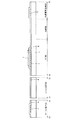
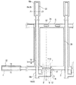
図1及び図2を参照して、本実施の形態に係るTFT基板の構成について説明する。図1は、FFS方式のTFT基板における画素部、及び、画素部(画素表示領域)外側のゲート端子部及びソース端子部の平面構成を示す図であり、図2は、その断面構成を示す図である。図2では、図1に示すX1−X2線、Y1−Y2線及びZ1−Z2線に沿った断面が示されている。X1−X2線に沿った断面は、画素の配設領域(画素部)に対応する。Y1−Y2線に沿った断面は、ゲート配線3(図2には図示せず)にゲート信号を供給するためのゲート端子4及びゲート端子パッド25の配設領域(ゲート端子部)に対応する。Z1−Z2線に沿った断面は、ソース配線18a,18b(図2には図示せず)に表示信号を印加するためのソース端子19a,19b及びソース端子パッド26の配設領域(ソース端子部)に対応する。
<Embodiment>
The configuration of the TFT substrate according to the present embodiment will be described with reference to FIGS. FIG. 1 is a diagram showing a planar configuration of a pixel portion and a gate terminal portion and a source terminal portion outside a pixel portion (pixel display region) in an FFS TFT substrate, and FIG. It is. FIG. 2 shows a cross section along the X1-X2 line, the Y1-Y2 line, and the Z1-Z2 line shown in FIG. A cross section along the line X1-X2 corresponds to a pixel arrangement region (pixel portion). The cross section along the Y1-Y2 line corresponds to the arrangement region (gate terminal portion) of the
図2に示すように、画素部は、X1−X2に沿って、TFTの配設領域である「TFT部」と、画素電極20及び対向電極27の配設領域である「透過画素部」と、対向電極27と共通配線5とが接続される「共通電極接続部」とを含んでいる。
As shown in FIG. 2, the pixel portion includes, along X1-X2, a “TFT portion” that is a TFT placement region and a “transmission pixel portion” that is a placement region of the
さて、本実施の形態に係るTFT基板は、絶縁基板1と、ゲート電極2と、共通配線5と、第1絶縁膜6と、半導体膜である半導体チャネル層7と、第2絶縁膜である保護絶縁層9,10,11と、第1ソース電極12と、第1ドレイン電極13と、第2ソース電極16と、第2ドレイン電極17と、画素電極20と、第3絶縁膜21と、対向電極27とを備えている。以下、本実施の形態に係るTFT基板の、これら構成要素と、これら以外の構成要素(ゲート配線3等)とについて説明する。
The TFT substrate according to the present embodiment is an insulating substrate 1, a
絶縁基板1には、例えばガラス等の透明性絶縁基板が用いられる。絶縁基板1上には、ゲート電極2、ゲート配線3、ゲート端子4及び共通配線5が配設されている。第1絶縁膜6は、ゲート電極2、ゲート配線3、ゲート端子4及び共通配線5を覆う。第1絶縁膜6は、TFT部ではゲート絶縁膜として機能するため、以下では「ゲート絶縁膜6」と記すこともある。
For the insulating substrate 1, for example, a transparent insulating substrate such as glass is used. On the insulating substrate 1, a
なお、図1に示されるように、ゲート配線3は横方向に延在しており、ゲート電極2及びゲート端子4と電気的に接続されている。ここでは、ゲート配線3におけるTFT部の部分(ゲート配線3の一部分)がゲート電極2となっており、ゲート電極2は、ゲート配線3の他の部分よりも幅が広くなっている。また、ゲート配線3におけるゲート端子部の部分(ゲート配線3の端部)がゲート端子4となっている。共通配線5は、ゲート配線3と平行に延在している。なお、図1及びこれ以降の平面図では、第1絶縁膜6、第3絶縁膜21の図示を適宜省略する。
As shown in FIG. 1, the
図1及び図2に示されるように、本実施の形態に係るTFT基板のTFT部では、ゲート電極2と、ゲート絶縁膜6(第1絶縁膜6)と、半導体チャネル層7と、保護絶縁層9と、第1ソース電極12と、第1ドレイン電極13と、第2ソース電極16と、第2ドレイン電極17とを備える。このうち、ゲート電極2及びゲート絶縁膜6については上述のとおりである。
As shown in FIGS. 1 and 2, in the TFT portion of the TFT substrate according to the present embodiment, a
半導体膜である半導体チャネル層7は、ゲート電極2上にゲート絶縁膜6を介して配設されている。なお、本実施の形態では、半導体チャネル層7は、平面視においてゲート電極2の外周よりも内側に配設されている。
A
ここでは、半導体チャネル層7は、酸化物半導体からなる。半導体チャネル層7の酸化物半導体には、例えば、酸化亜鉛(ZnO)系の酸化物半導体や、酸化亜鉛に酸化インジウム(In2O3)及び酸化すず(SnO2)を添加したInZnSnO系の酸化物半導体、または、酸化亜鉛系の酸化物半導体もしくは酸化亜鉛に酸化ガリウム(Ga2O3)及び酸化インジウム(In2O3)を添加したInGaZnO系の酸化物半導体などを用いることができる。半導体チャネル層7が酸化物半導体で構成されることにより、半導体チャネル層7にアモルファスシリコンを用いた構成よりも移動度を高めることができる。
Here, the
第2絶縁膜である保護絶縁層9,10,11は、半導体チャネル層7を覆う。ここでは、保護絶縁層10は半導体チャネル層7の一端の上部及び側部に設けられ、保護絶縁層11は半導体チャネル層7の他端の上部及び側部に設けられ、保護絶縁層9は、保護絶縁層10,11の間の半導体チャネル層7上に設けられている。なお、以下では、保護絶縁層9は、保護絶縁層10,11と連接されているものとして説明するが、保護絶縁層10,11と離間されてもよい。
The protective
第1ソース電極12は、保護絶縁層10、及び、保護絶縁層9の保護絶縁層10側の端部上、つまり第2絶縁膜の一端上に配設されている。第1ドレイン電極13は、保護絶縁層11、及び、保護絶縁層9の保護絶縁層11側の端部上、つまり第2絶縁膜の他端上に配設されている。
The
第1ソース電極12及び第1ドレイン電極13は、酸化物導電体以外の導電体からなるとともに、互いに離間している。本実施の形態では、第1ソース電極12及び第1ドレイン電極13の導電体に、金属または合金(例えばモリブデン(Mo)及びアルミニウム(Al)のそれぞれに他の元素を微量に添加してなる合金)が用いられる。
The
第2ソース電極16は、第1ソース電極12上に配設され、第1ソース電極12及び保護絶縁層9,10,11に設けられた第1コンタクトホール14を介して半導体チャネル層7と接続されている。第2ソース電極16は、酸化物導電体(例えばIn2O3とSnO2とを含むITO膜)からなる。なお、本実施の形態では、第1コンタクトホール14は、保護絶縁層9と保護絶縁層10との間に設けられている。
The
同様に、第2ドレイン電極17は、第1ドレイン電極13上に配設され、第1ドレイン電極13及び保護絶縁層9,10,11に設けられた第2コンタクトホール15を介して半導体チャネル層7と接続されている。第2ドレイン電極17は、酸化物導電体(例えばIn2O3とSnO2とを含むITO膜)からなる。なお、本実施の形態では、第2コンタクトホール15は、保護絶縁層9と保護絶縁層11との間に設けられている。
Similarly, the
次に、TFT基板のTFT部以外の構成要素についても説明する。 Next, components other than the TFT portion of the TFT substrate will be described.
図1に示されるように、第1ソース電極12は、ソース配線18aから分岐して設けられている。そして、同様に、第1ソース電極12上の第2ソース電極16は、ソース配線18a上のソース配線18bから分岐して設けられており、第1ソース電極12下の保護絶縁層10は、ソース配線18a下の保護絶縁層8から分岐して設けられている。そして、ソース配線18a,18bの端部には、それぞれソース端子19a,19bが設けられている。
As shown in FIG. 1, the
図2に示されるように、画素電極20は、第2ドレイン電極17と接続されており、第1絶縁膜6上に配設されている。本実施の形態では、画素電極20は、第2ドレイン電極17の一部を側方に延設して形成されている。
As shown in FIG. 2, the
第3絶縁膜21は、共通配線5上の第1絶縁膜6と、第2ソース電極16と、第2ドレイン電極17と、画素電極20とを覆う。本実施の形態では、第3絶縁膜21は、これら以外にも、ゲート端子4上の第1絶縁膜6や、保護絶縁層9なども覆う。
The third
ゲート端子パッド25は、第1絶縁膜6及び第3絶縁膜21に設けられたゲート用コンタクトホール22を介してゲート端子4と電気的に接続されている。ソース端子パッド26は、第3絶縁膜21に設けられたソース用コンタクトホール23を介してソース端子19a,19bと電気的に接続されている。
The
対向電極27は、画素電極20上に第3絶縁膜21を介して配設されている。そして、対向電極27は、第1絶縁膜6及び第3絶縁膜21に設けられた共通電極用コンタクトホール24(第3コンタクトホール)を介して共通配線5と接続されている。この対向電極27には、スリット開口部27aが設けられている。これにより、画素電極20と対向電極27との間に電圧が印加されると、対向電極27は、対向電極27上方にて横方向の電界を画素電極20との間に発生することが可能となっている。
The
<製造方法>
次に、本実施の形態に係るTFT基板の製造方法について、図3〜図14を参照しつつ説明する。なお、図3〜図14では、図1及び図2に示した構成要素に対応する構成要素に、それと同一符号が付されている。
<Manufacturing method>
Next, a manufacturing method of the TFT substrate according to the present embodiment will be described with reference to FIGS. 3 to 14, the same reference numerals are given to the components corresponding to the components shown in FIGS. 1 and 2.
まず、絶縁基板1を洗浄液または純水を用いて洗浄する。本実施の形態では、厚さが0.5mmであるガラス基板を絶縁基板1として用いた。そして、洗浄された絶縁基板1の一方の主面全面に、ゲート電極2及びゲート配線3などの材料である第1の導電膜を成膜する。
First, the insulating substrate 1 is cleaned using a cleaning liquid or pure water. In this embodiment, a glass substrate having a thickness of 0.5 mm is used as the insulating substrate 1. Then, a first conductive film made of a material such as the
第1の導電膜としては、例えば、クロム(Cr)、モリブデン(Mo)、チタン(Ti)、銅(Cu)、タンタル(Ta)、タングステン(W)、アルミニウム(Al)などの一般的な金属やこれらの金属元素を主成分として他の元素を1種類以上添加した合金等を用いることができる。ここで、主成分の元素とは、合金を構成する元素のうち、含有量が最も多い元素であることを意味する。また、これらの金属または合金を2層以上含む積層構造としてもよい。これらの金属または合金を用いることによって、比抵抗値が50μΩcm以下の低抵抗な導電膜を得ることができる。本実施の形態では、アルゴン(Ar)ガスを用いたスパッタリング法により、第1の導電膜として、厚さが200nmであるアルミニウム(Al)合金膜を成膜した。 Examples of the first conductive film include common metals such as chromium (Cr), molybdenum (Mo), titanium (Ti), copper (Cu), tantalum (Ta), tungsten (W), and aluminum (Al). Alternatively, an alloy containing one of these metal elements as a main component and one or more other elements added can be used. Here, the main component element means an element having the largest content among elements constituting the alloy. Moreover, it is good also as a laminated structure containing two or more layers of these metals or alloys. By using these metals or alloys, a low resistance conductive film having a specific resistance value of 50 μΩcm or less can be obtained. In this embodiment, an aluminum (Al) alloy film having a thickness of 200 nm is formed as the first conductive film by a sputtering method using an argon (Ar) gas.
その後、Al合金膜上にレジスト材を塗布し、第1回目の写真製版工程で当該レジスト材からフォトレジストパターンを形成し、当該フォトレジストパターンをマスクとして、Al合金膜を選択的にエッチングすることによりパターニングする。ここでのエッチングには、例えばリン酸、酢酸及び硝酸を含む溶液(PAN薬液)によるウェットエッチング法を用いることができる。その後、フォトレジストパターンを除去する。 Thereafter, a resist material is applied on the Al alloy film, a photoresist pattern is formed from the resist material in the first photolithography process, and the Al alloy film is selectively etched using the photoresist pattern as a mask. To pattern. For this etching, for example, a wet etching method using a solution (PAN chemical solution) containing phosphoric acid, acetic acid, and nitric acid can be used. Thereafter, the photoresist pattern is removed.
以上の結果、図3及び図4に示すように、絶縁基板1上のゲート電極2、ゲート配線3、ゲート端子4及び共通配線5が、上記第1の導電膜のパターニングによって形成される。
As a result, as shown in FIGS. 3 and 4, the
次に、絶縁基板1の上面全体に、第1絶縁膜6の材料である第1被加工絶縁膜を成膜する。本実施の形態では、第1被加工絶縁膜として、酸化シリコン(SiO)膜と窒化シリコン(SiN)膜とを、化学的気相成膜(CVD)法を用いて形成した。ここでは、厚さが50nmである酸化シリコン膜、及び、厚さが400nmである窒化シリコン膜を成膜した。なお、酸化シリコン膜は、水分(H2O)、水素(H2)、ナトリウム(Na)及びカリウム(K)のようなTFTの特性に影響を及ぼす不純物元素に対するバリア性(遮断性)が弱いので、第1被加工絶縁膜は、SiOの下層に例えばバリア性に優れるSiNなどを設けた積層構造とした。この第1被加工絶縁膜の大部分は、第1絶縁膜6及びゲート絶縁膜6となることから、以下、第1被加工絶縁膜を、ゲート絶縁膜6または第1絶縁膜6と記して説明する。
Next, a first processed insulating film that is a material of the first insulating
その後、第1絶縁膜6上に、半導体チャネル層7の材料である酸化物半導体膜を成膜する。本実施の形態では、その膜の酸化物半導体としてInとGaとZnとを含む酸化物(例えばInGaZnO)を用いる。その一例として、In:Ga:Zn:Oの原子組成比が1:1:1:4であるIn−Ga−Zn−Oターゲット[In2O3・Ga2O3・(ZnO)2]を用いたスパッタリング法により、InGaZnO酸化物半導体膜を成膜した。ただし、以上によって成膜された酸化物半導体膜では、通常、酸素の原子組成比が化学量論組成よりも少ないので、酸素イオン欠乏状態(上記の例ではOの組成比が4未満)となってしまう。このため、Arガスに酸素(O2)ガスを混合させてスパッタリングすることが好ましい。本実施の形態では、Arガスに対して分圧比で10%のO2ガスを添加した混合ガスを用いてスパッタリングし、厚さが50nmであるInGaZnO膜を成膜した。このように形成されたInGaZnO膜は、非晶質構造を有する。また、非晶質構造のInGaZnO膜は、一般的に結晶化温度が500℃以上であり、常温では膜中の大部分が非晶質構造のままで安定する。
Thereafter, an oxide semiconductor film which is a material of the
次に、第2回目の写真製版工程でフォトレジストパターンを形成し、これをマスクとして、酸化物半導体膜を選択的にエッチングすることによりパターニングする。ここでのエッチングには、例えばカルボン酸を含む薬液によるウェットエッチング法を用いることができる。カルボン酸を含む薬液としては、例えばシュウ酸を1〜10wt%の範囲で含むものが好ましい。本実施の形態では、シュウ酸5wt%と水とからなるシュウ酸系薬液を用いて酸化物半導体膜をエッチングした。その後、フォトレジストパターンを除去する。
Next, a photoresist pattern is formed in the second photolithography process, and the oxide semiconductor film is selectively etched using this as a mask for patterning. For the etching here, for example, a wet etching method using a chemical solution containing a carboxylic acid can be used. As a chemical | medical solution containing carboxylic acid, what contains oxalic acid in the range of 1-10 wt% is preferable, for example. In this embodiment, the oxide semiconductor film is etched using an oxalic acid chemical solution including
以上の結果、図5及び図6に示すように、ゲート電極2上に第1絶縁膜6を介して配設された半導体チャネル層7が、上記酸化物半導体膜のパターニングによって形成される。なお、第1絶縁膜6のうち、ゲート電極2と半導体チャネル層7とに挟まれた部分はゲート絶縁膜6として機能する。
As a result, as shown in FIGS. 5 and 6, the
次に、第1絶縁膜6及び半導体チャネル層7上に保護絶縁層8,9,10,11の材料である第2被加工絶縁膜を成膜する。本実施の形態では、第2被加工絶縁膜として、例えば厚さが100nmであるSiO膜を、CVD法を用いて形成した。
Next, a second processed insulating film, which is a material of the protective insulating
次いで、第2被加工絶縁膜上に第2の導電膜を成膜する。本実施の形態では、第2の導電膜として、モリブデン(Mo)及びアルミニウム(Al)のそれぞれに他の元素を微量に添加して得られる合金を積層させることによって積層構造を形成した。 Next, a second conductive film is formed over the second processed insulating film. In this embodiment, as the second conductive film, a stacked structure is formed by stacking alloys obtained by adding trace amounts of other elements to molybdenum (Mo) and aluminum (Al).
次に、第3回目の写真製版工程でフォトレジストパターンを形成し、これをマスクとして、第2の導電膜(ここではAl合金とMo合金との積層膜)を選択的にエッチングすることによりパターニングする。ここでのエッチングには、例えばリン酸、酢酸及び硝酸を含む溶液(PAN薬液)によるウェットエッチング法を用いることができる。本実施の形態では、リン酸70wt%と、酢酸7wt%と、硝酸5wt%と、水とからなるPAN薬液を用いてエッチングを行った。この段階では、下層の半導体チャネル層7は、第2被加工絶縁膜により保護されているので薬液によるダメージを受けない。
Next, a photoresist pattern is formed in the third photolithography process, and the second conductive film (here, a laminated film of Al alloy and Mo alloy) is selectively etched using this as a mask for patterning. To do. For this etching, for example, a wet etching method using a solution (PAN chemical solution) containing phosphoric acid, acetic acid, and nitric acid can be used. In the present embodiment, etching is performed using a PAN chemical solution including 70 wt% phosphoric acid, 7 wt% acetic acid, 5 wt% nitric acid, and water. At this stage, since the lower
その後、まだ除去されていないフォトレジストパターンと、上記パターニングが施された第2の導電膜とをマスクとして、第2被加工絶縁膜を選択的にエッチングすることによりパターニングする。ここでのエッチングには、例えばフッ素を含むガスを用いたドライエッチング法を用いることができる。本実施の形態では、六フッ化硫黄(SF6)に酸素(O2)を加えたガスを用いてドライエッチングした。O2ガスを添加することによって、エッチング時の下層の半導体チャネル層7の還元反応によるダメージを抑制することができる。その後、フォトレジストパターンを除去する。
Thereafter, patterning is performed by selectively etching the second processed insulating film using the photoresist pattern that has not yet been removed and the second conductive film subjected to the above patterning as a mask. For the etching here, for example, a dry etching method using a gas containing fluorine can be used. In this embodiment mode, dry etching is performed using a gas in which oxygen (O 2 ) is added to sulfur hexafluoride (SF 6 ). By adding O 2 gas, damage due to the reduction reaction of the lower
以上の結果、図7及び図8に示すように、一回の写真製版(ここでは第3回目の写真製版)の間に、半導体チャネル層7上の保護絶縁層9,10,11と、保護絶縁層8とが、上記第2被加工絶縁膜のパターニングによって形成されるとともに、電極体28と、ソース配線18aと、ソース端子19aとが、上記第2の導電膜のパターニングによって形成される。また、上記第2被加工絶縁膜のパターニングによって、半導体チャネル層7のソース領域上には第1コンタクトホール14が形成され、半導体チャネル層7のドレイン領域上には第2コンタクトホール15が形成される。
As a result of the above, as shown in FIG. 7 and FIG. 8, the protective insulating
なお、上述の電極体28とは、保護絶縁層10、及び、保護絶縁層9の保護絶縁層10側の端部上に配設された第1ソース電極12と、保護絶縁層11、及び、保護絶縁層9の保護絶縁層11側の端部上に配設された第1ドレイン電極13とが、保護絶縁層9上にて繋がった構造体である。なお、図8に示されるように、電極体28のうち、第1ソース電極12及び第1ドレイン電極13に対応する部分は、半導体チャネル層7上に直接的に配設されておらず、保護絶縁層9,10,11を介して半導体チャネル層7上に間接的に配設される。
The above-described
その後、半導体チャネル層7と、第1ソース電極12及び第1ドレイン電極13とを電気的に接続する第2ソース電極16及び第2ドレイン電極17の材料である第3の導電膜を成膜する。本実施の形態では、第3の導電膜として、光透過性の酸化物系導電膜であるITO膜(例えば、混合比がIn2O3の重量%:SnO2の重量%=90:10)を用いる。ITO膜は一般的に、常温中では結晶質(多結晶)構造が安定であるが、ここではスパッタリング法で、アルゴン(Ar)に水素(H)を含むガス、例えば、水素(H2)ガスまたは水蒸気(H2O)などを混合したガスを用いて成膜することにより、厚さが100nmであり、非晶質状態を有するITO膜を形成する。
Thereafter, a third conductive film that is a material of the
次に、第4回目の写真製版工程でフォトレジストパターンを形成し、これをマスクとして、第3の導電膜(非晶質ITO膜)を選択的にエッチングすることによりパターニングする。ここでのエッチングには、例えばシュウ酸5wt%と水とからなるシュウ酸系薬液によるウェットエッチング法を用いることができる。 Next, a photoresist pattern is formed in the fourth photolithography process, and patterning is performed by selectively etching the third conductive film (amorphous ITO film) using this as a mask. For this etching, for example, a wet etching method using an oxalic acid chemical solution composed of 5 wt% oxalic acid and water can be used.
その後、まだ除去されていないフォトレジストパターンと、上記パターニングが施された第3の導電膜とをマスクとして、電極体28を選択的にエッチングする。これにより、電極体28のうち第1ソース電極12及び第1ドレイン電極13を繋いでいた、保護絶縁層9上の部分が除去される。つまり、ソース電極(第1及び第2ソース電極12,16)とドレイン電極(第1及び第2ドレイン電極13,17)とが電気的に分離する。なお、ここでのエッチングには、例えばPAN薬液によるウェットエッチング法を用いることができる。その後、フォトレジストパターンを除去する。
Thereafter, the
以上の結果、図9及び図10に示すように、一回の写真製版(ここでは第4回目の写真製版)の間に、第2ソース電極16及び第2ドレイン電極17と、第2ドレイン電極17の画素表示領域に対応する部分である画素電極20と、ソース配線18bと、ソース端子19bとが、上記第3の導電膜のパターニングによって形成されるとともに、第1ソース電極12及び第1ドレイン電極13が、上記電極体28のパターニングによって形成される。
As a result of the above, as shown in FIGS. 9 and 10, the
なお、ITOなどからなる酸化物導電体からなる第2ソース電極16及び第2ドレイン電極17は、それぞれ第1コンタクトホール14及び第2コンタクトホール15を介して下層の半導体チャネル層7に直接接続されている。このような構成によれば、酸化物導電体以外の導電体からなる第1ソース電極12及び第1ドレイン電極13が半導体チャネル層7に直接接続される構成よりも、半導体チャネル層7のソース領域及びドレイン領域における還元反応を抑制することができる。この結果、半導体チャネル層7の特性劣化を抑制することができる。
The
以上によって第2ソース電極16、第2ドレイン電極17及び画素電極20を形成した後、絶縁基板1の上面全体に、第3絶縁膜21の材料である第3被加工絶縁膜を成膜する。本実施の形態では、第3被加工絶縁膜として、厚さが200nmである酸化シリコン(SiO)膜と、厚さが100nmである窒化シリコン(SiN)膜とを、この順にCVD法を用いて成膜した。
After forming the
そして、第5回目の写真製版工程でフォトレジストパターンを形成し、これをマスクとして、第3被加工絶縁膜及び第1絶縁膜6を選択的にエッチングすることによりパターニングする。ここでのエッチングには、例えばフッ素を含むガスを用いたドライエッチング法を用いることができる。本実施の形態では、六フッ化硫黄(SF6)に酸素(O2)を加えたガスを用いてドライエッチングした。その後、フォトレジストパターンを除去する。
Then, a photoresist pattern is formed in the fifth photolithography process, and the third
以上の結果、図11及び図12に示すように、ゲート端子部のゲート用コンタクトホール22、ソース端子部のソース用コンタクトホール23、及び、共通配線接続部の共通電極用コンタクトホール24が設けられた第3絶縁膜21が、上記第3被加工絶縁膜のパターニングによって形成される。
As a result, as shown in FIGS. 11 and 12, a
その後、ゲート用コンタクトホール22を介してゲート端子4と電気的に接続されたゲート端子パッド25と、ソース用コンタクトホール23を介してソース端子19a,19bと電気的に接続されたソース端子パッド26と、共通電極用コンタクトホール24を介して共通配線5と電気的に接続された対向電極27との材料である第4の導電膜を成膜する。本実施の形態では、第4の導電膜として透光性導電膜を成膜する。透光性導電膜としては、ITO膜(例えば、混合比がIn2O3の重量%:SnO2の重量%=90:10)を用いる。ITO膜は一般的に、常温中では結晶質(多結晶)構造が安定であるが、ここではスパッタリング法で、アルゴン(Ar)に水素(H)を含むガス、例えば、水素(H2)ガスまたは水蒸気(H2O)などを混合したガスを用いて成膜することにより、厚さが100nmであり、非晶質状態を有するITO膜を形成する。
Thereafter, a
そして、第6回目の写真製版工程でフォトレジストパターンを形成し、これをマスクとして、第4の導電膜(非晶質ITO膜)を選択的にエッチングすることによりパターニングする。ここでのエッチングには、例えばシュウ酸5wt%と水とからなるシュウ酸系薬液によるウェットエッチング法を用いることができる。その後、フォトレジストパターンを除去する。 Then, a photoresist pattern is formed in the sixth photolithography process, and patterning is performed by selectively etching the fourth conductive film (amorphous ITO film) using this as a mask. For this etching, for example, a wet etching method using an oxalic acid chemical solution composed of 5 wt% oxalic acid and water can be used. Thereafter, the photoresist pattern is removed.
以上の結果、図1及び図2に示すように、ゲート用コンタクトホール22を介してゲート端子4と電気的に接続されたゲート端子パッド25と、ソース用コンタクトホール23を介してソース端子19a,19bと電気的に接続されたソース端子パッド26と、共通電極用コンタクトホール24を介して共通配線5と電気的に接続された対向電極27とが、上記第4の導電膜のパターニングによって形成される。なお、当該パターニングによって、対向電極27にはスリット開口部27aが設けられる。以上により、図1及び図2に示したFFS−LCD用のTFT基板が完成する。
As a result, as shown in FIGS. 1 and 2, the
液晶表示パネルの組み立ての際は、完成したTFT基板の表面に配向膜やスペーサを形成する。配向膜は、液晶を配列させるための膜であり、ポリイミド等で構成される。また、別途作製したカラーフィルタや配向膜を備えた対向基板を、本実施の形態に係るTFT基板と対向配置させて貼り合わせる。このとき、スペーサによってTFT基板と対向基板との間に隙間が形成され、その隙間に液晶層を形成して封止することによって、FFSモードの液晶表示パネルが形成される。これにより、当該液晶表示パネルを備える液晶表示装置は、対向電極27と画素電極20との間に発生する電界のうち、対向電極27に関して画素電極20と逆側に発生する横方向の電界によって、液晶を駆動することが可能となっている。
When the liquid crystal display panel is assembled, an alignment film and a spacer are formed on the surface of the completed TFT substrate. The alignment film is a film for aligning liquid crystals and is made of polyimide or the like. In addition, a counter substrate provided with a separately manufactured color filter or alignment film is disposed so as to face the TFT substrate according to this embodiment. At this time, a gap is formed between the TFT substrate and the counter substrate by the spacer, and a liquid crystal layer is formed and sealed in the gap, thereby forming an FFS mode liquid crystal display panel. As a result, the liquid crystal display device including the liquid crystal display panel has a horizontal electric field generated on the opposite side of the
最後に、液晶表示パネルの外側に偏光板、位相差板及びバックライトユニット等を配設することによって液晶表示装置が完成する。 Finally, a liquid crystal display device is completed by disposing a polarizing plate, a retardation plate, a backlight unit, and the like outside the liquid crystal display panel.
<実施の形態のまとめ>
以上のような本実施の形態に係るTFT基板及び液晶表示装置によれば、酸化物半導体からなる半導体チャネル層7上に、保護絶縁層9,10,11を介して、酸化物導電体以外の導電体(例えば金属層または合金層)からなる第1ソース電極12及び第1ドレイン電極13が配設される。このような構成によれば、ソース電極及びドレイン電極を形成する加工プロセスの際における、半導体チャネル層7のダメージを抑制することができる。したがって、TFTの特性及び信頼性を高めることができる。
<Summary of Embodiment>
According to the TFT substrate and the liquid crystal display device according to the present embodiment as described above, a layer other than the oxide conductor is provided on the
また、本実施の形態では、酸化物導電体からなる第2ソース電極16及び第2ドレイン電極17が、半導体チャネル層7と、酸化物導電体以外の導電体からなる第1ソース電極12及び第1ドレイン電極13との間を接続する。このような構成によれば、従来技術では、半導体チャネル層7と第1ソース電極12及び第1ドレイン電極13との間に生じていた還元反応を抑制することができる。これにより、当該界面でのコンタクト特性を向上させることができ、オン電流値や移動度の値が向上するので、TFTの特性及び信頼性を高めることができる。
In the present embodiment, the
なお、仮に、半導体チャネル層7が、平面視においてゲート電極2の外周(端部)からはみ出して配設されている場合には、ゲート電極2の厚さにより当該ゲート電極2の外周に形成される段差部で耐圧が悪くなったり、段差部上方に形成されるソース電極及びドレイン電極の段切れ(段差部に起因する断線や断裂)が発生したりする可能性がある。
If the
これに対して、本実施の形態では、半導体チャネル層7は、平面視においてゲート電極2の外周よりも内側に配設されている。これにより、ゲート電極2の上記段差部上方には、第1絶縁膜6と、保護絶縁層10,11が形成されることになるので、ゲート電極2と、ソース電極及びドレイン電極との間の耐圧を向上させることができる。また、半導体チャネル層7を覆うように保護絶縁層9,10,11が形成されることにより、ゲート電極2と第1ソース電極12との間の電気的ショート(短絡)不良を抑制することができる。また、ソース電極及びドレイン電極のカバレッジ特性(被覆性)を高めることができるので、上記段差部に起因するソース電極及びドレイン電極の段切れ不良の発生を抑制することができる。
On the other hand, in the present embodiment, the
また、本実施の形態に係るTFT基板の製造方法によれば、一回の写真製版の間に、保護絶縁層9,10,11と、第1ソース電極12及び第1ドレイン電極13となる電極体28とを形成し、一回の写真製版の間に第2ソース電極16、第2ドレイン電極17及び画素電極20と、第1ソース電極12及び第1ドレイン電極13とを形成する。このような製造方法によれば、半導体チャネル層7を保護する保護絶縁層9,10,11を形成するための専用の写真製版を行わなくて済むことから、生産能力の低下を抑制することができるとともに、写真製版のマスク枚数の増加に伴う製造コストの増加を抑制することができる。
Moreover, according to the manufacturing method of the TFT substrate according to the present embodiment, the protective insulating
以上のように、本実施の形態によれば、酸化物半導体からなる半導体チャネル層7上に、保護絶縁層9,10,11を介して、酸化物導電体以外の導電体からなる第1ソース電極12及び第1ドレイン電極13が配設される。これにより、第1ソース電極12及び第1ドレイン電極13を形成する際の成膜及びエッチングによる、半導体チャネル層7へのダメージを抑制することができるのでTFTの特性及び信頼性を高めることができる。また、TFTの半導体チャネル層7に、移動度の高い酸化物半導体膜を用いることにより、動作速度の速いTFTの基板、及びそれを用いた液晶表示装置を、高い歩留まりで製造することができる。つまり、高性能のTFT基板及び液晶表示装置を、生産性良く製造することができる。
As described above, according to the present embodiment, the first source made of a conductor other than the oxide conductor is provided on the
<変形例>
図13及び図14を参照して、本実施の形態の変形例に係るTFT基板の構成について説明する。図13は、本変形例に係るFFS方式のTFT基板における画素部、及び、画素部(画素表示領域)外側のゲート端子部及びソース端子部の平面構成を示す図であり、図14は、その断面構成を示す図である。図14では、図13に示すX1−X2線、Y1−Y2線及びZ1−Z2線に沿った断面が示されている。X1−X2線に沿った断面は、画素の配設領域(画素部)に対応する。Y1−Y2線に沿った断面は、ゲート配線3(図14には図示せず)にゲート信号を供給するためのゲート端子4及びゲート端子パッド25の配設領域(ゲート端子部)に対応する。Z1−Z2線に沿った断面は、ソース配線18a,18b(図14には図示せず)に表示信号を印加するためのソース端子19a,19b及びソース端子パッド26の配設領域(ソース端子部)に対応する。
<Modification>
With reference to FIGS. 13 and 14, the structure of a TFT substrate according to a modification of the present embodiment will be described. FIG. 13 is a diagram illustrating a planar configuration of a pixel portion and a gate terminal portion and a source terminal portion outside the pixel portion (pixel display region) in the FFS type TFT substrate according to this modification, and FIG. It is a figure which shows a cross-sectional structure. FIG. 14 shows a cross section taken along line X1-X2, line Y1-Y2, and line Z1-Z2 shown in FIG. A cross section along the line X1-X2 corresponds to a pixel arrangement region (pixel portion). The cross section along the Y1-Y2 line corresponds to an arrangement region (gate terminal portion) of the
本変形例では、実施の形態1の共通配線5及び画素電極20の少なくともいずれか一方のパターンを一部変更して、画素電極20の少なくとも一部が、平面視において共通配線の少なくとも一部と重なるように構成されている。このような重なり領域を形成することによって、画素電極20には液晶容量に加えて補助容量が形成されるため、画素電極20に書き込まれた映像信号の電荷の保持特性が向上する。したがって、輝度ムラのような表示不良を抑制することができ、さらに高い表示品質を有するFFSモードの液晶表示パネル(液晶表示装置)を実現することができる。
In this modification, at least one pattern of at least one of the
なお、上記の実施の形態1及び変形例においては、本発明をFFSモードの液晶表示パネル(液晶表示装置)へ適用した場合を例示して説明を行った。しかし、TFT部と当該TFT部に接続される画素電極20に関する構造については、FFS−LCDに限られず、酸化物導電体を画素電極に用いたLCDであれば、例えば、TN(Twisted Nematic)モードの透過型LCDにも適用することができる。
In the first embodiment and the modification, the case where the present invention is applied to an FFS mode liquid crystal display panel (liquid crystal display device) has been described as an example. However, the structure relating to the TFT portion and the
TNモードの透過型LCDに適用した場合においては、実施の形態1のTFT部の基本的な構成と画素電極20との接続構造までは同様の構成を用いることができ、TFT基板上に配設される共通配線5及び対向電極27の構成が省略される。そして、TFT基板上に配設される対向電極27に代えて、カラーフィルタや配向膜を備えた対向基板上に画素表示領域全面にわたってITO膜などの酸化物導電体により形成される対向電極が配設される。そのような構成において、TFT基板上に配設される画素電極20と、対向基板上に配設される対向電極との間に発生する電界によって液晶を駆動するように部分的に変更するとよい。
When applied to a TN mode transmissive LCD, the same configuration can be used up to the basic configuration of the TFT portion of the first embodiment and the connection structure with the
このように変更した構成においても、実施の形態1において得られる基本的な効果が得られる。つまり、第1ソース電極12及び第1ドレイン電極13を形成する際の成膜及びエッチングによる、半導体チャネル層7へのダメージを抑制することができるので、TFTの特性及び信頼性を高めることができる効果が得られる。あるいは、TFTの半導体チャネル層7に、移動度の高い酸化物半導体膜を用いることにより、動作速度の速いTFTの基板、及びそれを用いた液晶表示装置を、高い歩留りで製造することができる効果が得られる。つまり、高性能のTFT基板及び液晶表示装置を、生産性良く製造することができる効果について同様に得ることができる。
Even in such a modified configuration, the basic effects obtained in the first embodiment can be obtained. That is, since damage to the
なお、本発明は、その発明の範囲内において、実施の形態を適宜、変形、省略することが可能である。 In the present invention, the embodiments can be appropriately modified and omitted within the scope of the invention.
1 絶縁基板、2 ゲート電極、5 共通配線、6 第1絶縁膜、7 半導体チャネル層、9,10,11 保護絶縁層、12 第1ソース電極、13 第1ドレイン電極、14 第1コンタクトホール、15 第2コンタクトホール、16 第2ソース電極、17 第2ドレイン電極、20 画素電極、21 第3絶縁膜、24 共通電極用コンタクトホール、27 対向電極、28 電極体。 DESCRIPTION OF SYMBOLS 1 Insulating substrate, 2 Gate electrode, 5 Common wiring, 6 1st insulating film, 7 Semiconductor channel layer, 9, 10, 11 Protective insulating layer, 12 1st source electrode, 13 1st drain electrode, 14 1st contact hole, 15 second contact hole, 16 second source electrode, 17 second drain electrode, 20 pixel electrode, 21 third insulating film, 24 common electrode contact hole, 27 counter electrode, 28 electrode body.
Claims (12)
前記絶縁基板上に配設されたゲート電極と、
前記ゲート電極を覆う第1絶縁膜と、
前記ゲート電極上に前記第1絶縁膜を介して配設された、酸化物半導体からなる半導体膜と、
前記半導体膜を覆う第2絶縁膜と、
前記第2絶縁膜の一端上に配設された、酸化物導電体以外の導電体からなる第1ソース電極と、
前記第2絶縁膜の他端上に配設された、酸化物導電体以外の導電体からなる第1ドレイン電極と、
前記第1ソース電極上に配設され、前記第1ソース電極及び前記第2絶縁膜に設けられた第1コンタクトホールを介して前記半導体膜と接続された、酸化物導電体からなる第2ソース電極と、
前記第1ドレイン電極上に配設され、前記第1ドレイン電極及び前記第2絶縁膜に設けられた第2コンタクトホールを介して前記半導体膜と接続された、酸化物導電体からなる第2ドレイン電極と、
前記第2ドレイン電極の一部を延設して形成された画素電極と、
前記第1絶縁膜と、前記第2ソース電極と、前記第2ドレイン電極と、前記画素電極とを覆う第3絶縁膜と
を備える、薄膜トランジスタ基板。 An insulating substrate;
A gate electrode disposed on the insulating substrate;
A first insulating film covering the gate electrode;
A semiconductor film made of an oxide semiconductor disposed on the gate electrode via the first insulating film;
A second insulating film covering the semiconductor film;
A first source electrode made of a conductor other than an oxide conductor, disposed on one end of the second insulating film;
A first drain electrode made of a conductor other than an oxide conductor, disposed on the other end of the second insulating film;
A second source made of an oxide conductor disposed on the first source electrode and connected to the semiconductor film via a first contact hole provided in the first source electrode and the second insulating film Electrodes,
A second drain made of an oxide conductor disposed on the first drain electrode and connected to the semiconductor film via a second contact hole provided in the first drain electrode and the second insulating film Electrodes,
A pixel electrode formed by extending a part of the second drain electrode;
A thin film transistor substrate comprising: a first insulating film; a second source electrode; a second drain electrode; and a third insulating film covering the pixel electrode.
前記絶縁基板上に配設され、前記第1絶縁膜により覆われる共通配線と、
前記画素電極上に第3絶縁膜を介して配設され、前記第1絶縁膜及び前記第3絶縁膜に設けられた第3コンタクトホールを介して前記共通配線と接続されるとともに、横方向の電界を前記画素電極との間に発生することが可能な対向電極と
をさらに備える、薄膜トランジスタ基板。 The thin film transistor substrate according to claim 1,
A common wiring disposed on the insulating substrate and covered with the first insulating film;
A third insulating film is disposed on the pixel electrode, and is connected to the common wiring through a third contact hole provided in the first insulating film and the third insulating film, and in the lateral direction. A thin film transistor substrate, further comprising: a counter electrode capable of generating an electric field between the pixel electrode.
前記半導体膜は、
平面視において前記ゲート電極の外周よりも内側に配設された、薄膜トランジスタ基板。 The thin film transistor substrate according to claim 1 or 2,
The semiconductor film is
A thin film transistor substrate disposed inside the outer periphery of the gate electrode in plan view.
前記画素電極は、前記第1絶縁膜上に配設され、
前記画素電極の少なくとも一部は、
平面視において前記共通配線の少なくとも一部と重なる、薄膜トランジスタ基板。 The thin film transistor substrate according to claim 2,
The pixel electrode is disposed on the first insulating film,
At least a portion of the pixel electrode is
A thin film transistor substrate that overlaps at least a part of the common wiring in a plan view.
前記薄膜トランジスタ基板と対向配置された対向基板とを備え、
前記画素電極と、前記薄膜トランジスタ基板または前記対向基板に配設された対向電極との間に発生する電界によって液晶を駆動する、液晶表示装置。 A thin film transistor substrate according to claim 1;
A counter substrate disposed opposite to the thin film transistor substrate,
A liquid crystal display device that drives liquid crystal by an electric field generated between the pixel electrode and the thin film transistor substrate or the counter electrode provided on the counter substrate.
前記酸化物半導体膜上に当該酸化物半導体膜を覆うように絶縁層を形成する工程と、
前記絶縁層を介して前記酸化物半導体膜を覆う導電膜を形成する工程と、
少なくとも前記酸化物半導体膜上に一部が残るように前記絶縁層及び前記導電膜を1回の写真製版でパターニングすることによって、前記酸化物半導体膜上に第2絶縁膜を、前記第2絶縁膜上に電極体を形成する工程と、
前記電極体を形成する工程後に、前記電極体を分離することによって、前記第2絶縁膜上で離間する第1ソース電極及び第1ドレイン電極を形成する工程と
を備える、薄膜トランジスタ基板の製造方法。 Preparing an insulating substrate having a gate electrode and an oxide semiconductor film formed on the gate electrode through a first insulating film;
Forming an insulating layer on the oxide semiconductor film so as to cover the oxide semiconductor film;
Forming a conductive film covering the oxide semiconductor film through the insulating layer;
The insulating layer and the conductive film are patterned by one photolithography so that at least part of the oxide semiconductor film remains on the oxide semiconductor film, whereby a second insulating film is formed on the oxide semiconductor film. Forming an electrode body on the film;
Forming a first source electrode and a first drain electrode separated on the second insulating film by separating the electrode body after the step of forming the electrode body.
一回の写真製版の間に、第2ソース電極、第2ドレイン電極及び画素電極をパターニングによって形成するとともに前記電極体を分離するパターニングを行うことによって、前記第1ソース電極及び前記第1ドレイン電極を形成する工程を行う、薄膜トランジスタ基板の製造方法。 A method of manufacturing a thin film transistor substrate according to claim 6,
The first source electrode and the first drain electrode are formed by patterning the second source electrode, the second drain electrode, and the pixel electrode by patterning and separating the electrode body during one photolithography process. The manufacturing method of the thin-film transistor substrate which performs the process of forming.
前記電極体を形成する工程にて、前記絶縁層及び前記電極体に、前記酸化物半導体膜の一部を露出する第1及び第2コンタクトホールをエッチングによって形成し、
前記第1ソース電極上から前記第1コンタクトホールを介して前記酸化物半導体膜上に延在する酸化物導電体からなる第2ソース電極を形成するとともに、前記第1ドレイン電極上から前記第2コンタクトホールを介して前記酸化物半導体膜上に延在する酸化物導電体からなる第2ドレイン電極を形成する工程をさらに備える、薄膜トランジスタ基板の製造方法。 A method of manufacturing a thin film transistor substrate according to claim 6 or 7,
In the step of forming the electrode body, first and second contact holes that expose a part of the oxide semiconductor film are formed in the insulating layer and the electrode body by etching,
Forming a second source electrode made of an oxide conductor extending on the oxide semiconductor film from the first source electrode through the first contact hole, and forming the second source electrode on the first drain electrode; A method for manufacturing a thin film transistor substrate, further comprising a step of forming a second drain electrode made of an oxide conductor extending on the oxide semiconductor film through a contact hole.
前記電極体を形成する工程において形成される前記電極体は、前記第1ソース電極が形成されるソース電極形成領域から前記第1ドレイン電極が形成されるドレイン電極形成領域にわたって一体に形成された導電膜からなる、薄膜トランジスタ基板の製造方法。 A method of manufacturing a thin film transistor substrate according to claim 6,
The electrode body formed in the step of forming the electrode body is a conductive body integrally formed from a source electrode formation region where the first source electrode is formed to a drain electrode formation region where the first drain electrode is formed. A method for producing a thin film transistor substrate comprising a film.
前記第2ドレイン電極の形成とともに、前記第2ドレイン電極と一体化された酸化物導電体からなる画素電極を形成する、薄膜トランジスタ基板の製造方法。 A method of manufacturing a thin film transistor substrate according to claim 8,
A method of manufacturing a thin film transistor substrate, wherein the pixel electrode made of an oxide conductor integrated with the second drain electrode is formed together with the formation of the second drain electrode.
前記第1ソース電極及び前記第1ドレイン電極は、酸化物導電体以外の導電体からなる、薄膜トランジスタ基板の製造方法。 A method of manufacturing a thin film transistor substrate according to claim 6,
The method of manufacturing a thin film transistor substrate, wherein the first source electrode and the first drain electrode are made of a conductor other than an oxide conductor.
前記第2ドレイン電極に電気的に接続される画素電極を形成する工程と、前記画素電極上に第3絶縁膜を形成し、当該第3絶縁膜上に対向電極を形成する工程とをさらに備える、薄膜トランジスタ基板の製造方法。 A method of manufacturing a thin film transistor substrate according to any one of claims 7, 8 , and 10 ,
Forming a pixel electrode electrically connected to the second drain electrode; and forming a third insulating film on the pixel electrode and forming a counter electrode on the third insulating film. A method for manufacturing a thin film transistor substrate.
Priority Applications (3)
| Application Number | Priority Date | Filing Date | Title |
|---|---|---|---|
| JP2014229474A JP6422310B2 (en) | 2014-11-12 | 2014-11-12 | Thin film transistor substrate, method for manufacturing the same, and liquid crystal display device |
| US14/884,050 US9553109B2 (en) | 2014-11-12 | 2015-10-15 | Thin film transistor substrate, method for manufacturing the same, and liquid crystal display |
| US15/372,671 US9941409B2 (en) | 2014-11-12 | 2016-12-08 | Method for manufacturing a thin film transistor substrate |
Applications Claiming Priority (1)
| Application Number | Priority Date | Filing Date | Title |
|---|---|---|---|
| JP2014229474A JP6422310B2 (en) | 2014-11-12 | 2014-11-12 | Thin film transistor substrate, method for manufacturing the same, and liquid crystal display device |
Publications (3)
| Publication Number | Publication Date |
|---|---|
| JP2016096171A JP2016096171A (en) | 2016-05-26 |
| JP2016096171A5 JP2016096171A5 (en) | 2017-12-21 |
| JP6422310B2 true JP6422310B2 (en) | 2018-11-14 |
Family
ID=55912880
Family Applications (1)
| Application Number | Title | Priority Date | Filing Date |
|---|---|---|---|
| JP2014229474A Active JP6422310B2 (en) | 2014-11-12 | 2014-11-12 | Thin film transistor substrate, method for manufacturing the same, and liquid crystal display device |
Country Status (2)
| Country | Link |
|---|---|
| US (2) | US9553109B2 (en) |
| JP (1) | JP6422310B2 (en) |
Families Citing this family (3)
| Publication number | Priority date | Publication date | Assignee | Title |
|---|---|---|---|---|
| CN104409415B (en) * | 2014-12-03 | 2017-03-15 | 重庆京东方光电科技有限公司 | A kind of array base palte and preparation method thereof, display device |
| JP6689108B2 (en) * | 2016-03-22 | 2020-04-28 | 三菱電機株式会社 | Thin film transistor substrate and manufacturing method thereof |
| CN107146818B (en) * | 2017-06-27 | 2020-02-18 | 京东方科技集团股份有限公司 | Thin film transistor, manufacturing method thereof, array substrate and display device |
Family Cites Families (14)
| Publication number | Priority date | Publication date | Assignee | Title |
|---|---|---|---|---|
| JPS62235784A (en) | 1986-04-07 | 1987-10-15 | Sharp Corp | Thin film transistor |
| US6449026B1 (en) | 1999-06-25 | 2002-09-10 | Hyundai Display Technology Inc. | Fringe field switching liquid crystal display and method for manufacturing the same |
| JP4483235B2 (en) | 2003-09-01 | 2010-06-16 | カシオ計算機株式会社 | Transistor array substrate manufacturing method and transistor array substrate |
| JP5006598B2 (en) | 2005-09-16 | 2012-08-22 | キヤノン株式会社 | Field effect transistor |
| TWI318010B (en) * | 2006-11-09 | 2009-12-01 | Au Optronics Corp | Pixel structure and fabricating method thereof |
| JP4496237B2 (en) * | 2007-05-14 | 2010-07-07 | 株式会社 日立ディスプレイズ | Liquid crystal display |
| JP5095865B2 (en) | 2009-12-21 | 2012-12-12 | シャープ株式会社 | Active matrix substrate, display panel including the same, and method for manufacturing active matrix substrate |
| KR20120024241A (en) * | 2010-09-06 | 2012-03-14 | 삼성모바일디스플레이주식회사 | Organic light emitting display and manufacturing method thereof |
| JP5275523B2 (en) * | 2010-11-04 | 2013-08-28 | シャープ株式会社 | Display device, semiconductor device, and display device manufacturing method |
| KR20120060664A (en) * | 2010-12-02 | 2012-06-12 | 삼성전자주식회사 | Display apparatus and fabrication method of the same |
| JP6076626B2 (en) * | 2012-06-14 | 2017-02-08 | 株式会社ジャパンディスプレイ | Display device and manufacturing method thereof |
| JP6103854B2 (en) * | 2012-08-10 | 2017-03-29 | 三菱電機株式会社 | Thin film transistor substrate |
| JP6124668B2 (en) * | 2013-04-26 | 2017-05-10 | 三菱電機株式会社 | Thin film transistor substrate and manufacturing method thereof |
| US10083990B2 (en) * | 2014-08-29 | 2018-09-25 | Lg Display Co., Ltd. | Thin film transistor substrate and display device using the same |
-
2014
- 2014-11-12 JP JP2014229474A patent/JP6422310B2/en active Active
-
2015
- 2015-10-15 US US14/884,050 patent/US9553109B2/en active Active
-
2016
- 2016-12-08 US US15/372,671 patent/US9941409B2/en active Active
Also Published As
| Publication number | Publication date |
|---|---|
| JP2016096171A (en) | 2016-05-26 |
| US9941409B2 (en) | 2018-04-10 |
| US9553109B2 (en) | 2017-01-24 |
| US20170092775A1 (en) | 2017-03-30 |
| US20160133649A1 (en) | 2016-05-12 |
Similar Documents
| Publication | Publication Date | Title |
|---|---|---|
| JP6124668B2 (en) | Thin film transistor substrate and manufacturing method thereof | |
| WO2016195039A1 (en) | Active matrix substrate and method for manufacturing same, display device using active matrix substrate | |
| JP6437126B2 (en) | Thin film transistor substrate and manufacturing method thereof | |
| US9911765B2 (en) | Thin film transistor substrate including thin film transistor formed of oxide semiconductor and method for manufacturing the same | |
| JP6103854B2 (en) | Thin film transistor substrate | |
| JP6785563B2 (en) | Non-linear devices, array substrates, and methods for manufacturing array substrates | |
| JP6422310B2 (en) | Thin film transistor substrate, method for manufacturing the same, and liquid crystal display device | |
| JP2019169660A (en) | Thin-film transistor substrate, display device, and method for manufacturing thin-film transistor substrate | |
| JP6025595B2 (en) | Thin film transistor manufacturing method | |
| JP2020096095A (en) | Thin film transistor substrate, display device, and liquid crystal display device | |
| US9929186B2 (en) | Thin film transistor substrate and method for manufacturing the same | |
| JP6120794B2 (en) | Thin film transistor substrate and manufacturing method thereof | |
| JP6768462B2 (en) | Thin film transistor, thin film transistor substrate, liquid crystal display device, and thin film transistor manufacturing method | |
| JP2012124194A (en) | Thin film transistor, active matrix substrate, and manufacturing method for thin film transistor and active matrix substrate | |
| JP6180200B2 (en) | Active matrix substrate and manufacturing method thereof | |
| JP2020031107A (en) | Thin film transistor, thin film transistor substrate, and method of manufacturing the same | |
| JP6671155B2 (en) | Thin film transistor substrate | |
| JP2015220387A (en) | Display panel substrate, display panel, display device and display panel substrate manufacturing method | |
| JP2019153811A (en) | Display panel substrate, display panel, and display device |
Legal Events
| Date | Code | Title | Description |
|---|---|---|---|
| A521 | Request for written amendment filed |
Free format text: JAPANESE INTERMEDIATE CODE: A523 Effective date: 20171108 |
|
| A621 | Written request for application examination |
Free format text: JAPANESE INTERMEDIATE CODE: A621 Effective date: 20171108 |
|
| A977 | Report on retrieval |
Free format text: JAPANESE INTERMEDIATE CODE: A971007 Effective date: 20180709 |
|
| A131 | Notification of reasons for refusal |
Free format text: JAPANESE INTERMEDIATE CODE: A131 Effective date: 20180724 |
|
| A521 | Request for written amendment filed |
Free format text: JAPANESE INTERMEDIATE CODE: A523 Effective date: 20180905 |
|
| TRDD | Decision of grant or rejection written | ||
| A01 | Written decision to grant a patent or to grant a registration (utility model) |
Free format text: JAPANESE INTERMEDIATE CODE: A01 Effective date: 20180918 |
|
| A61 | First payment of annual fees (during grant procedure) |
Free format text: JAPANESE INTERMEDIATE CODE: A61 Effective date: 20181016 |
|
| R150 | Certificate of patent or registration of utility model |
Ref document number: 6422310 Country of ref document: JP Free format text: JAPANESE INTERMEDIATE CODE: R150 |
|
| R250 | Receipt of annual fees |
Free format text: JAPANESE INTERMEDIATE CODE: R250 |
|
| R250 | Receipt of annual fees |
Free format text: JAPANESE INTERMEDIATE CODE: R250 |
|
| R250 | Receipt of annual fees |
Free format text: JAPANESE INTERMEDIATE CODE: R250 |