JP6422012B2 - Magnetic detector - Google Patents
Magnetic detector Download PDFInfo
- Publication number
- JP6422012B2 JP6422012B2 JP2014028183A JP2014028183A JP6422012B2 JP 6422012 B2 JP6422012 B2 JP 6422012B2 JP 2014028183 A JP2014028183 A JP 2014028183A JP 2014028183 A JP2014028183 A JP 2014028183A JP 6422012 B2 JP6422012 B2 JP 6422012B2
- Authority
- JP
- Japan
- Prior art keywords
- frequency
- magnetic
- noise
- averaging
- sensor
- Prior art date
- Legal status (The legal status is an assumption and is not a legal conclusion. Google has not performed a legal analysis and makes no representation as to the accuracy of the status listed.)
- Active
Links
Images


Landscapes
- Measuring Magnetic Variables (AREA)
Description
本発明は、磁気センサの出力信号におけるノイズの低減を図ることのできる磁気検出装置に関するものであり、特に、繰り返し周波数を有する電流パルスによって駆動される磁気センサを有する磁気検出装置に関するものである。 The present invention relates to a magnetic detection device capable of reducing noise in an output signal of a magnetic sensor, and more particularly to a magnetic detection device having a magnetic sensor driven by a current pulse having a repetition frequency.
繰り返し周波数を有する電流パルスによって駆動される磁気センサを有する磁気検出装置が知られている。例えば、特許文献1に記載の磁気検出装置がそれである。特許文献1に記載の磁気検出センサは、いわゆる磁気インピーダンスセンサ(MIセンサ)であり、アモルファスワイヤに高周波のパルス状の電流を印加することに磁気の検出を行なうものである。
2. Description of the Related Art A magnetic detection device having a magnetic sensor driven by a current pulse having a repetition frequency is known. For example, this is the magnetic detection device described in
一般に、アナログ信号を出力するセンサからの出力信号は、一定の時間間隔で数値化(サンプリング)されて信号処理が行なわれることとなる。このとき、その時間間隔よりも短い周期の信号、より正確には、その時間間隔の2倍よりも短い周期の信号は、サンプリング周波数以下の信号に変化してしまう。これをエイリアスノイズ(alias noise、折り返し雑音)といい、このような関係は標本化定理によるものである。このエイリアスノイズが元の信号に含まれることにより、元の信号を破壊してしまうこととなる。かかる問題に対し、一般的にはかかるエイリアスノイズを回避するため、センサの出力信号を、サンプリング周波数の1/2以上の周波数成分を除去するローパスフィルタに通過させたのち、サンプリングを行なうことが広く行なわれている。 In general, an output signal from a sensor that outputs an analog signal is digitized (sampled) at a certain time interval and subjected to signal processing. At this time, a signal having a period shorter than the time interval, more precisely, a signal having a period shorter than twice the time interval changes to a signal having a sampling frequency or less. This is called alias noise, and this relationship is due to the sampling theorem. When the alias noise is included in the original signal, the original signal is destroyed. In general, in order to avoid such alias noise, it is common to perform sampling after passing the output signal of the sensor through a low-pass filter that removes a frequency component that is 1/2 or more of the sampling frequency. It is done.
ところで、特許文献1に記載された磁気インピーダンスセンサは、サンプリング周波数に相当する周波数が、アモルファスワイヤに印可されるパルス電流の周波数となる。そして、そのパルス電流の周期中に極めて鋭い矩形波を与えるものである。そのため、磁気インピーダンスセンサにおける検出コイルの出力も、少なくともサンプリング周波数以上の、あるいはその数倍以上の高周波成分を含む。そのため、上述のように検出コイルの出力をサンプリング周波数の1/2以上の周波数成分を除去するローパスフィルタに通過させてしまうと、本来の信号以外の高周波成分が全て除去されてしまうため、分解能の低下の大きな要因となりうる。
Incidentally, in the magnetic impedance sensor described in
このように、繰り返し周波数を有する電流パルスによって駆動される磁気センサの出力信号に対しては、エイリアスノイズを除去するための従来技術の適用が困難な場合があり、エイリアスノイズの除去についての新たな方法が必要であった。 As described above, it may be difficult to apply the conventional technique for removing alias noise to an output signal of a magnetic sensor driven by a current pulse having a repetition frequency. A method was needed.
本発明は以上の事情を背景として為されたもので、その目的とするところは、繰り返し周波数を有する電流パルスによって駆動される磁気センサの出力信号に対して、エイリアスノイズの除去を有効に行なうことにより精度のよい計測が可能な磁気検出装置を提供することにある。 The present invention has been made against the background of the above circumstances, and its object is to effectively remove alias noise from the output signal of a magnetic sensor driven by a current pulse having a repetition frequency. An object of the present invention is to provide a magnetic detection device capable of measuring with higher accuracy.
かかる目的を達成するため発明は、(a)繰り返し周波数を有する電流パルスによって駆動される磁気センサと、該磁気センサからの出力信号を処理する信号処理部とを有する磁気検出装置であって、(b)該信号処理部は、(b−1)前記磁気センサの出力信号のサンプリングを行うサンプルホールド回路と、(b−2)該サンプルホールド回路におけるサンプリング周波数を前記繰り返し周波数と等しくされ、前記繰り返し周波数近傍のノイズがシャノンのサンプリング定理に従ってエイリアス信号となって繰り返し周波数よりも低周波のノイズとなる場合に、該低周波のノイズの振幅が半分以下となるように、該繰り返し周波数の周期内において平均化区間を設け、該平均化区間において平均化処理を行う平均化処理部と、を有すること、を特徴とする。 In order to achieve this object, the invention provides a magnetic detection device having (a) a magnetic sensor driven by a current pulse having a repetition frequency, and a signal processing unit for processing an output signal from the magnetic sensor, b) the signal processing unit includes: (b-1) a sample and hold circuit that samples the output signal of the magnetic sensor; and (b-2) a sampling frequency in the sample and hold circuit is made equal to the repetition frequency, and the repetition When the noise near the frequency becomes an alias signal according to Shannon's sampling theorem and becomes a noise having a frequency lower than the repetition frequency, the amplitude of the low frequency noise is reduced to half or less within the period of the repetition frequency. the averaging interval is provided, this having an average processing unit for performing averaging process in the averaging interval And features.
かかる発明によれば、設定された平均化区間に対して平均化処理部による平均化処理が行なわれるので、エイリアスノイズの振幅を半分以下とすることができるので、エイリアスノイズの影響を低減することができる。ひいては磁気検出装置の分解能を向上させることができる。 According to this invention, since the averaging process is performed on the set averaging interval by the averaging processing unit, the amplitude of the alias noise can be reduced to half or less, thereby reducing the influence of the alias noise. Can do. As a result, the resolution of the magnetic detection device can be improved.
また、好適には、(a)前記繰り返し周波数またはその近傍の周波数を中心周波数とするアナログノッチフィルタ、もしくは前記繰り返し周波数またはその近傍の周波数以上の周波数成分を通過させるハイパスフィルタを有し、(b)前記平均化処理部による平均化処理に加えて該アナログノッチフィルタもしくはハイパスフィルタにより前記磁気センサの出力を処理すること、を特徴とする。このようにすれば、アナログノッチフィルタあるいはハイパスフィルタによって磁気センサの出力が処理されるので、前記平均化処理によってはノイズの低減ができない場合においてもエイリアスノイズの低減について一定の効果が得られる。
Also, preferably, it has a highpass filter for passing (a) the repetition frequency or analog notch filter for a center frequency in the vicinity thereof or the repetition frequency or frequency or higher frequency components in the vicinity thereof, ( b) the averaging process by the averaging process unit by applying strong point the analog notch filter or high-pass filter processing the output of said magnetic sensor, characterized by. In this way, since the output of the magnetic sensor is processed by the analog notch filter or the high-pass filter, even if the noise cannot be reduced by the averaging process, a certain effect can be obtained in reducing alias noise.
以下、本発明の一実施例について、図面を参照しつつ詳細に説明する。 Hereinafter, an embodiment of the present invention will be described in detail with reference to the drawings.
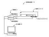
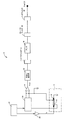
図1は、本発明の磁気検出装置の構成の一例を示した図である。図1に示すように、磁気検出装置10は、磁気センサ12と回路部18とを含んで構成されている。このうち、磁気センサ12は繰り返し周波数を有する電流パルスによって駆動される磁気センサであり、本実施例においては磁気インピーダンスセンサ(MIセンサ)である。
FIG. 1 is a diagram showing an example of the configuration of the magnetic detection device of the present invention. As shown in FIG. 1, the
磁気センサ12は、感磁部の磁束変化を検出する検出コイル13と、アモルファスワイヤ14とを含んで構成されている。また検出コイル13はそれぞれ、中空のコイル状に設けられており、コイルの両端の電圧を後述する電気回路を用いて検出することができるようにされており、本実施例においてはその一方が接地されている。具体的には、磁気センサ12に設けられた検出コイル13の両端の電位差voutが検出可能とされている。磁気センサ12に設けられた検出コイル13の形状はで、例えば、線径60μm、内径0.2mm、巻数500、長さ10mmのコイルである。
The magnetic sensor 12 includes a detection coil 13 that detects a change in magnetic flux in the magnetic sensing portion and an
また、検出コイル13の中空部分には、アモルファスワイヤ14が通されている。本実施例においては、図1に示す様にアモルファスワイヤ14は長手方向に延びる棒状の形状を有しており、一本のアモルファスワイヤ14が検出コイル13の中空部分を通る(貫く)様に配設されている。
An
本実施例においては、アモルファスワイヤ14は、例えば線径30μmで、検出コイル13の両端から一定長さだけ長いものが用いられる。アモルファスワイヤ14の両端には、そのアモルファスワイヤ14に電流iinを印加することができるように配線が設けられている。図1の例においては、アモルファスワイヤ14の一端に、後述する発振器22からの電流iinが印加されるようになっており、他端は接地されている。本実施例においてアモルファスワイヤ14のうち、磁気センサ12の検出コイル13内に位置する部分は感磁部として機能している。
In this embodiment, the
図2は、図1に示す本実施例の磁気検出装置10のうち、磁気センサ12と、回路部18の構成の一部であって磁気センサ12との入出力を行なう部分とを説明する図である。回路部18は、前記磁気センサ12を駆動するための電気信号iinを入力する駆動回路部19と、磁気センサ12からの出力信号Voutを処理するための検出回路部20とを有する。また、本実施例においては、回路部18には、具体的には例えばモニタなどの表示装置である出力装置90が接続されており、算出された磁気センサ12における磁界強度に関する情報が表示される。なお、出力装置90は本発明の磁気検出装置10に必須ではなく、例えば、算出された磁気センサ12における磁界強度に関する情報が他の機器に電子的な情報として伝達されるようにしてもよい。
FIG. 2 is a diagram for explaining the magnetic sensor 12 and a part of the configuration of the circuit unit 18 that performs input / output with the magnetic sensor 12 in the
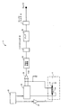
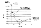
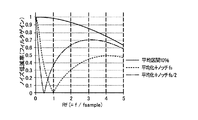
図2に示す回路部18のうち、発振器22からは、アモルファスワイヤ14に通電される電流iinなどの元となるパルス信号、すなわち矩形波が生成される。この矩形波は、アンプ24によって所定の増幅が行なわれ、アモルファスワイヤ14に印加される。このように、発信機22とアンプ24は駆動回路部19を構成する。本実施例においては例えば、パルス信号の振幅が2〜3Vとなるように増幅が行なわれる。図3はアモルファスワイヤに印可されるパルス信号の繰り返し周波数とセンサの感度との関係の一例を説明する図である。この図3に示されるセンサの感度が良好となる繰り返し周波数が選択される。具体的には図3の例においては、繰り返し周波数が10kHz以上においてはセンサの感度がほぼ一定であるので、繰り返し周波数が10kHzとされる。また、パルス幅は、磁気インピーダンスセンサが高感度化するように、予め実験的にあるいはシミュレーションにより得られた値とされる。具体的には、アモルファスワイヤ14のインピーダンス変化が最も顕著な周波数が10MHzである場合には、パルス幅が50nsとなり、デューティー比は0.0005となる。
In the circuit unit 18 shown in FIG. 2, an
サンプルホールド回路26は、検出コイル13の両端電位差、すなわち両端における電圧の差(起電力)が入力される。このサンプルホールド回路26においては、アモルファスワイヤ14に印加するパルス信号の立ち上がり(通電開始)によりコイルに発生する誘導電圧について、その立ち上がり(図4の時刻t1)からピーク(図4の時刻t2)を含む時間範囲において積分して出力を行なう。具体的には例えば前記時間範囲は10ns〜50nsのように設定される。このため、サンプルホールド回路26には前述の発振器22によって出力されるパルス信号が入力されており、サンプルホールド回路26はこのパルス信号の立ち上がりをスイッチとして作動を行なう。また、バッファアンプ28はそれぞれ、サンプルホールド回路26の出力を増幅する。
The
なお、検出コイル13においては、図4に示す様に、アモルファスワイヤ14に印加されるパルス信号における立ち上がり(通電開始)によって検出コイル13に発生する誘導電圧の波形と、パルス信号における立ち下がり(通電遮断)によって検出コイル13に発生する誘導電圧との変動とが連続して発生するよう、すなわち、パルス信号における立ち上がり(通電開始)によって検出コイル13に発生する誘導電圧の波形とパルス信号における立ち下がり(通電遮断)によって検出コイル13に発生する誘導電圧との波形との間に誘導電圧が例えば0に留まる時間がないようにされている。前述の検出コイル13の形状として例示した、線径60μm、内径0.2mm、巻数500、長さ10mmのコイルは、本実施例においてこの条件を満たすものである。
In the detection coil 13, as shown in FIG. 4, the waveform of the induced voltage generated in the detection coil 13 due to the rise (start of energization) in the pulse signal applied to the
続いて、平均化処理部30により平均化処理が行なわれる。この平均化処理は、設定された平均化区間において入力信号の平均化を行なうものである。平均化処理部30の詳細について説明する。
Subsequently, the averaging
まず、サンプルホールド回路26において行なわれる積分演算によるノイズの低減について検討する。検出コイル13の出力信号Voutに対する、サンプルホールド回路におけるサンプリングの積算間隔をTs[sec]、高周波ノイズ成分の周波数をfs[Hz]、振幅をAs[V]、ノイズ位相をxとした時、ノイズ低減効果は、
上記(1)式のうち、分数で表された部分は、サンプリングの際の平均化区間にノイズの周期が全て入ってノイズが打ち消される区間と、平均化区間からはみ出た1周期未満の区間の比に振幅を乗じたものである。また、天井関数部分は、該はみ出た区間のノイズの平均の振幅を表している。
First, the reduction of noise by the integration operation performed in the
In the above equation (1), the fractional part includes the interval in which the entire noise period is entered in the averaging interval at the time of sampling and the noise is canceled, and the interval that is less than one cycle that protrudes from the averaging interval. The ratio is multiplied by the amplitude. The ceiling function portion represents the average amplitude of noise in the protruding section.
ところで、上記(1)式を計算すると、次のようになる。
位相xの平均化を行なうための積分区間を決めるため、上記(2)式の絶対値の中が零となるための式は、
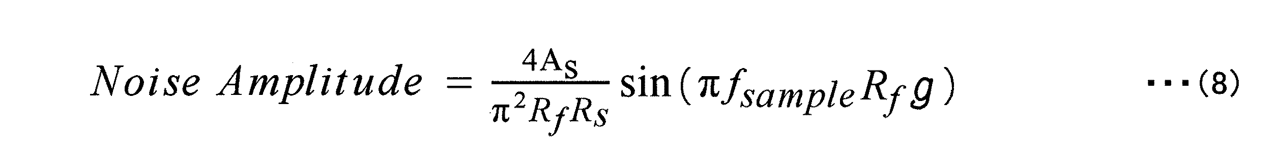
この処理は、平均化区間を設けることによりノイズの位相がランダム化された後に平均化されるものである。この処理により、ノイズの信号強度(振幅の大きさ)は、上記(5)式に示すように得られる。サンプリング間隔Tsを大きくできればノイズの振幅が小さくなるので、ノイズ低減効果が大きいことが分かる。また、周波数fsが大きい高周波ノイズに対してノイズ低減効果が大きいことが分かる。 This process is performed after the noise phase is randomized by providing an averaging section. By this processing, the signal strength (amplitude magnitude) of noise is obtained as shown in the above equation (5). It can be seen that if the sampling interval Ts can be increased, the noise amplitude is reduced, so that the noise reduction effect is great. Moreover, it turns out that the noise reduction effect is large with respect to the high frequency noise with large frequency fs.
続いて、かかる平均化によるエイリアスノイズの低減について説明する。サンプリング周波数をfsampleとし、サンプルホールド回路26におけるデータサンプリング周期(Sampling Interval)とサンプリング積算間隔との比をRs(以下、「周期比Rs」という。)とすると、
前記(5)式を前記Rfおよびfsampleを用いて書き換えると、
このようにすれば、上記(10)式で示されるように、ノイズの振幅を区間、周波数を用いることなく、区間の比、周波数の比を用いて表すことができている。
Rewriting equation (5) using Rf and fsample,
In this way, as indicated by the above equation (10), the amplitude of noise can be expressed using the ratio of the section and the ratio of the frequency without using the section and the frequency.
エイリアスノイズは、サンプリング周波数の二分の一以上の周波数成分を有するノイズであることから、周波数比Rfが1/2以上の周波数のノイズが全てエイリアスノイズとなる。そのため、サンプリング周波数fsampleが高いほどエイリアスノイズとなる帯域は狭まることとなる。 Alias noise is noise having a frequency component that is one-half or more of the sampling frequency. Therefore, all noise having a frequency ratio Rf of 1/2 or more is alias noise. Therefore, the higher the sampling frequency fsample, the narrower the band that becomes alias noise.
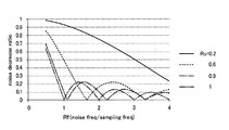
続いて、サンプルホールド回路26における周期比Rsの選び方について説明する。上記(10)式を、複数の周期比Rsの値について解き、周波数比Rfに対する、出力信号に含まれるノイズの大きさ(振幅)と平均化処理後の信号に含まれるノイズの大きさ(振幅)との比を図示したものが図5である。ここでAsはAs=1とした。
Next, how to select the period ratio Rs in the sample and hold
図5に示すように、周波数比Rfが1/2以上の帯域においてエイリアスノイズの大きさを低減できていることが分かる。特に、周期比Rsが0.6以上の場合に急激にエイリアスノイズの低減効果が顕著である。また、周期比Rsが0.9以上である場合には、サンプリング周波数以上の帯域(周波数比Rfが1以上の帯域)におけるエイリアスノイズは、ほぼ20%以下に低減される。 As shown in FIG. 5, it can be seen that the magnitude of alias noise can be reduced in a band where the frequency ratio Rf is 1/2 or more. In particular, when the cycle ratio Rs is 0.6 or more, the effect of reducing alias noise is remarkable. Further, when the cycle ratio Rs is 0.9 or more, alias noise in a band higher than the sampling frequency (band where the frequency ratio Rf is 1 or higher) is reduced to approximately 20% or lower.
このようにして平均化処理部30により平均化処理が行なわれ、エイリアスノイズの影響が低減された後、ハイパスフィルタ36によって所定の周波数、例えば0.3Hzより低い周波数成分は遮断される。さらにアンプ38により増幅が行われるとともに、ローパスフィルタ40によって、所定の周波数、例えば30Hzより高い周波数成分が遮断されて出力Eout(V)が出力される。この出力Eout(V)を予め得られている換算方法によって磁界強度に変換することにより、測定対象物50の発生する磁界強度を得ることができる。
In this way, the averaging
上述の実施例によれば、設定された平均化区間に対して平均化処理部30による平均化処理が行なわれるので、エイリアスノイズの振幅を半分以下とすることができるので、エイリアスノイズの影響を低減することができる。ひいては磁気検出装置の分解能を向上させることができる。
According to the above embodiment, since the averaging process is performed by the averaging
続いて、本発明の別の実施例について説明する。以下の説明において、実施例相互に共通する部分については、同一の符号を付して説明を省略する。 Subsequently, another embodiment of the present invention will be described. In the following description, portions common to the embodiments are denoted by the same reference numerals and description thereof is omitted.
図6は、本発明の別の実施例における回路部59を説明する図である。本実施例における回路部59では、図2の回路部19に比べて、ノッチフィルタ42が設けられている点において異なる。
FIG. 6 is a diagram for explaining a circuit unit 59 in another embodiment of the present invention. The circuit portion 59 in this embodiment is different from the circuit portion 19 in FIG. 2 in that a
図7は、サンプルホールド回路26からの出力信号voutと、それに対してノッチフィルタ42による処理後の信号とをシミュレーションにより比較する図である。図7の例においては、サンプルホールド回路26におけるサンプリング周波数を500kHzとする一方、ノッチフィルタの中心周波数も500kHzである。図7に示すように、理想的なノッチフィルタによる処理によれば、信号強度を悪化させることがほとんどないことがわかる。
FIG. 7 is a diagram comparing the output signal vout from the sample-and-
一方、図8は、サンプルホールド回路26からの出力信号voutの周波数スペクトルを表した図である。図8に示すように、磁気インピーダンスセンサであるセンサ12から出力される信号においては1MHzよりも高周波側には多くの高周波成分が多く含まれるので、それら高周波成分をカットすると信号強度への影響が大きくなる。これを考慮する場合、設けるノッチフィルタは例えば図8において四角く囲んだ領域である、500kHz付近のみをカットするものであることが望ましい。
On the other hand, FIG. 8 is a diagram showing the frequency spectrum of the output signal vout from the
図9は、本実施例におけるノッチフィルタ42の構成を説明する図である。例えば、抵抗R1、R2、R3の抵抗値をR1=R2=R3=3.3kΩ、キャパシタC1、C2、C3の容量をそれぞれC1=400pF、C2=C3=100pFとすると、ノッチフィルタ42の中心周波数f0は341kHzとなる。
FIG. 9 is a diagram illustrating the configuration of the
図10は、サンプルホールド回路26からの出力信号voutが、前述の実施例1の場合における処理、すなわち平均化処理のみの場合と、本実施例2の場合、すなわち、平均化処理に加え、ノッチフィルタによる処理を行なった場合とで、ノイズの減衰率を比較する図であって、図3に対応する図である。図8において実線で記載されたのは平均化処理のみを行なった場合であり、パルス繰り返し周期に対して平均化区間を10%とした平均化処理を行なった場合を示している。また、一点鎖線で示したのは、上記平均化処理に加え、サンプリング周波数fsampleを中心周波数とするノッチフィルタによる処理を行なった場合、二点鎖線で示したのは、平均化処理に加え、サンプリング周波数fsampleの半分、すなわちfsample/2を中心周波数とするノッチフィルタによる処理を行なった場合の例を示している。
FIG. 10 shows the case where the output signal vout from the sample and hold
図10に示すように、同一の条件においては、全般的に平均化処理のみを行なう場合に比べて、平均化処理に加えてノッチフィルタによる処理を行なった場合の方がノイズをより低減できていることが分かる。特に、平均化処理によってはあまり低減されることのないサンプリング周波数よりも小さい周波数のノイズ(周波数比Rfが1よりも小さいノイズ)に対してより効果的にその影響を低減できていることがわかる。 As shown in FIG. 10, under the same conditions, noise can be further reduced when the processing using the notch filter is performed in addition to the averaging processing as compared with the case where only the averaging processing is generally performed. I understand that. In particular, it can be seen that the influence of noise having a frequency lower than the sampling frequency (noise having a frequency ratio Rf smaller than 1) that is not significantly reduced by averaging processing can be reduced more effectively. .
図11は、サンプルホールド回路26からの出力信号voutのスペクトルと、ノッチフィルタの周波数特性を重ね合わせて示した図である。この図11に示すように、中心周波数を341kHzとしたノッチフィルタの場合、2MHzにおけるゲインは約0.8である。すなわち、信号強度が約2割低下することとなる。このように、図10に示すようなノイズの除去効果と図11に示すような信号強度の低下度合いはトレードオフの関係にあるので、両者のバランスを取ることができる値となるようにノッチフィルタの中心周波数を決定することとなる。この場合、ノッチフィルタにおける抵抗およびキャパシタの性能を変更することでその中心周波数を実現することができる。
FIG. 11 is a diagram in which the spectrum of the output signal vout from the
前述の実施例2によれば、アナログノッチフィルタ42によって磁気センサの出力が処理されるので、前記平均化処理部30による平均化処理に加えて、さらにエイリアスノイズの低減を行なうことができる。また、前記平均化処理によってはノイズの低減ができない場合においてもエイリアスノイズの低減について一定の効果が得られる。
According to the second embodiment described above, since the output of the magnetic sensor is processed by the
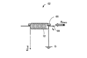
続いて、本発明の別の実施例について説明する。図12は、本発明の磁気検出装置12に用いられる別の磁気センサ62の概要を説明する図である。基本構成を概念的に説明する図である。磁気センサ62はそれぞれ、磁性材料としてのアモルファス材料66、導電体としての導線68、コイル72を有して構成されている。このうち、アモルファス材料66は長手状の形状を有するアモルファスワイヤである。導線68はそれぞれアモルファス材料66に近接して設けられており、アモルファス材料70の長手方向に平行となるように伸びている。コイル72はそれぞれ、アモルファス材料66および導線68をそれぞれその内部に含むようなソレノイド状のコイルとして設けられている。なお、アモルファス材料66と導線68とは例えば空間が設けられたり、絶縁体が介在させられることなどによりそれぞれ電気的に接合していない状態とされている。後述するように、センサの構成としてはこのようなものに限られず、例えばアモルファス材料66の形状は長手方向に延びるものであれば、図12に示すような棒状のものに限定されるものではない。また、コイル72とアモルファス材料66および導線68との位置関係は、コイル72の内部にアモルファス材料66および導線68を含むものに限られず、アモルファス材料66によって誘導される電流を発生することができるようにコイル72が配置されればよい。なお、本実施例における磁気センサ62を、iPAセンサ(induced para−magnetization alignment sensor)と呼ぶ。
Subsequently, another embodiment of the present invention will be described. FIG. 12 is a diagram for explaining the outline of another
図13は、センサ62の電気的な構成を説明する図である。導線68には図示しない発振機22(図12参照)から供給される周期的に変化する矩形波状のパルス電流Ieが流れる。また、コイル72の起電力Ecoilはそれぞれサンプルホールド回路26(図12参照)に出力される。
FIG. 13 is a diagram illustrating the electrical configuration of the
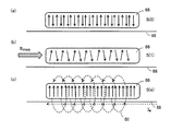
図14を用いて、センサ62、すなわちiPAセンサの動作原理の概要を説明する。図14は、iPAセンサのうち、アモルファス材料66および導線68のみを記載したものであり、アモルファス材料66中の磁荷の分布を説明する図である。アモルファス材料66中の矢印のそれぞれが磁荷の向きを概念的に示している。図14のうち、(a)はiPAセンサに外部磁界が加わっていない無磁界状態、あるいは環境磁界のみが印加されているいわゆるコントロール状態S(0)を示している。図14の(b)は、計測対象からの磁界Bmesが印加された状態S(1)を示しており、(c)は導線68に十分な励起電流Ieが印加された際の状態S(e)を示している。
The outline of the operation principle of the
図14の(a)および(b)に示すように、アモルファス材料66における磁化は、外部から印加される微小な磁界により、例えば図14(a)のS(0)から図14(b)のS(1)のように変化させられる。すなわち、前記コントロール状態S(0)では、アモルファス材料66の磁化(Mam)は例えばその長手方向に直交する方向を向いている。一方、磁界Bmesが印加された状態S(1)では、一部の容易磁化方向を形成する磁気モーメントの配向が変化する。一方、図14(c)に示すように、アモルファス材料66に近接して配設された導線68に十分な励起電流Ieが流された場合には、その励起電流Ieが図14(c)における点線で示されるような磁界Beを発生する。そして、アモルファス材料66中の磁化の一定量は、その磁界Beの方向に整列した状態S(e)となる。このように、励起電流Ieが流されることにより磁化が整列するため、一過性の磁界を発生することとなる。ここで、励起電流Ieを流す前の磁界、より詳細にはその磁界の下でのアモルファス材料66の磁化の状態により、磁化の整列に伴って生ずる前記一過性の磁界の大きさが異なる。具体的には、アモルファスワイヤ66が状態S(0)から状態S(e)に変化する際の一過性の磁界と、状態S(1)から状態S(e)に変化する際の一過性の磁界とはその大きさが異なる。
As shown in FIGS. 14A and 14B, the magnetization in the
このようにしてアモルファスワイヤ66が生ずる一過性の磁界を、コイル72(図12、13参照)により、それらコイル72における起電力の変化Ecoilとして検出する。この起電力の変化は、励起電流Ieの通電前後のアモルファス材料66における磁化の変化に対応するものとなる。具体的には、励起電流Ieの通電前におけるアモルファスワイヤ66が受けていた磁界に応じて異なり、通電前におけるアモルファスワイヤ66の状態がS(0)であった場合には、
{Mam(S(e))−Mam(S(0))}/Δt
となり、通電前におけるアモルファスワイヤ66の状態がS(1)であった場合には、
{Mam(S(e))−Mam(S(1))}/Δt
となる。このように、コイル72における起電力の変化Ecoilは、計測対象の磁界Bmesを反映したものとなり、起電力の変化Ecoilに基づいて磁界Bmesの大きさを算出し得ることとなる。なお、前記Δtは磁化が整列するのに要する時間であり、例えばナノ秒単位の時間である。
The transient magnetic field generated by the
{Mam (S (e))-Mam (S (0))} / Δt
When the state of the
{Mam (S (e))-Mam (S (1))} / Δt
It becomes. Thus, the electromotive force change Ecoil in the
本実施例においては、励起電流Ieはパルス電流であるので、電流が通電されアモルファス材料66の磁化が整列される励起状態期間と、通電が停止され、磁化が元の状態に戻る弛緩状態期間とが高周波で繰り返される。そのため、コイル72における誘導起電力の前記励起状態期間と弛緩状態期間とにおける差を検出することができる。また、これを複数回くり返して平均値などを算出することもできる。
In this embodiment, since the excitation current Ie is a pulse current, an excitation state period in which the current is supplied and the magnetization of the
前記励起電流Ieは、環境磁界、すなわち通常の室内環境において受ける地磁気中においてアモルファスワイヤ66の内部磁化を整列させることができる程度の電流となるようにその大きさが定められる。具体的には、図12乃至図14に示すように導線68が直線状のものである場合には、励起電流Ieの通電時におけるその近傍の誘導磁界Beの大きさは、アンペールの法則より
Be=μ0I/2πr
のように近似される。ここでμ0は真空の透磁率(=4π×10−7(T/A/m)であり、rは導線68の中心からの距離である。ここで、励起電流Ieの大きさIを200mAとすると、導線68の中心から1000μm(10−3m)の距離におけるアモルファス材料66にも4×10−5Tの誘導磁界Beを加えることができる。この値は地磁気に匹敵するものであるから、地磁気の下においてアモルファス材料66の磁化を整列するのに十分であると考えられる。
The magnitude of the excitation current Ie is determined so as to be a current that can align the internal magnetization of the
It is approximated as follows. Here, μ0 is the vacuum permeability (= 4π × 10 −7 (T / A / m), and r is the distance from the center of the
このようなiPAセンサによって構成される磁気センサ62も、導体68に印加される繰り返し周波数を有するパルス電流によって駆動される磁気センサであるので、前述の実施例におけるMIセンサによって構成される磁気センサ12と同様に、その出力信号を平均化処理部30による平均化処理、あるいはそれに加えてもしくはそれに代えてノッチフィルタによる処理により、エイリアスノイズの影響を低減することができる。
Since the
以上、本発明の実施例を図面に基づいて詳細に説明したが、本発明はその他の態様においても適用される。 As mentioned above, although the Example of this invention was described in detail based on drawing, this invention is applied also in another aspect.
例えば、前述の実施例においては、平均化処理部30やノッチフィルタ42による処理は、単独のセンサ出力をサンプルホールド回路26により処理したものに対して行なわれたが、このような態様に限られない。例えば、複数のセンサ12もしくは62を複数用い、それらを差動させる場合においては、一対のセンサの差動出力をサンプルホールド回路により処理し、その出力を平均化処理部30により平均化したり、ノッチフィルタ42による処理を行なうことも可能である。
For example, in the above-described embodiment, the processing by the averaging
また、前述の実施例2においては、所定の周波数近傍の帯域成分を通過させないノッチフィルタ42が用いられたが、これに代えて、所定周波数以下の帯域成分を通過させないハイパスフィルタを用いることも可能である。この場合、前記所定周波数を超える帯域成分はそのハイパスフィルタを通過させられるため、信号強度が低下する割合を抑えることができる。
In the second embodiment described above, the
また、前述の実施例2においては、平均化処理部30による平均化処理が行なわれた後でノッチフィルタ42による処理が行なわれたが、そのような態様に限られず、これらの順序を逆に行なってもよい。なお、複数のチャンネルに設けられた磁気センサ12、62からの信号がマルチプレックス処理される場合においても適用は可能である。かかる場合にはデータの積算範囲や平均化区間がサンプリング周期よりも短くなるので、エイリアスノイズの影響が顕著であるところ、ノッチフィルタ42によりエイリアスノイズが現れるサンプリング周波数付近あるいはそれより小さい周波数帯域をカットすることによりエイリアスノイズの影響を低減できる。この場合、ノッチフィルタ42による処理は、バッファアンプによるデマルチプレックス処理よりも前段で、1チャンネル毎、すなわち各センサの信号ごとにアナログフィルタで行なえばよい。
Further, in the above-described second embodiment, the averaging process by the averaging
また、前述の実施例においては、磁気センサとして磁気インピーダンスセンサ(MIセンサ)およびiPAセンサが用いられたが、このようなものに限定されず、繰り返し周波数を有するパルス電流に依って駆動される磁気センサであれば本発明が同様に適用可能である。 In the above-described embodiments, the magnetic impedance sensor (MI sensor) and the iPA sensor are used as the magnetic sensor. However, the present invention is not limited to such a magnetic sensor, and the magnetic sensor is driven by a pulse current having a repetition frequency. The present invention can be similarly applied to any sensor.
その他、一々例示はしないが、本発明はその趣旨を逸脱しない範囲内において種々の変更が加えられて実施されるものである。 In addition, although not illustrated one by one, the present invention is implemented with various modifications within a range not departing from the gist thereof.
10:磁気検出装置
12、62:磁気センサ
18、59:回路部
30:平均化処理部
42:ノッチフィルタ
10: Magnetic detection device 12, 62: Magnetic sensor 18, 59: Circuit unit 30: Averaging processing unit 42: Notch filter
Claims (2)
該信号処理部は、前記磁気センサの出力信号のサンプリングを行うサンプルホールド回路と、
該サンプルホールド回路におけるサンプリング周波数を前記繰り返し周波数と等しくされ、前記繰り返し周波数近傍のノイズがシャノンのサンプリング定理に従ってエイリアス信号となって繰り返し周波数よりも低周波のノイズとなる場合に、該低周波のノイズの振幅が半分以下となるように、該繰り返し周波数の周期内において平均化区間を設け、該平均化区間において平均化処理を行う平均化処理部と、を有すること、
を特徴とする磁気検出装置。 A magnetic detection device having a magnetic sensor driven by a current pulse having a repetition frequency and a signal processing unit for processing an output signal from the magnetic sensor,
The signal processing unit includes a sample and hold circuit that samples an output signal of the magnetic sensor;
When the sampling frequency in the sample and hold circuit is made equal to the repetition frequency, and the noise in the vicinity of the repetition frequency becomes an alias signal according to Shannon's sampling theorem and becomes a lower frequency noise than the repetition frequency, the low frequency noise as amplitude is equal to or less than half, the repeated averaging period provided in the period of the frequency, to have, an averaging processing unit for performing averaging process in the averaging interval,
Magnetic detection device characterized by the above.
前記平均化処理部による平均化処理に加えて該アナログノッチフィルタもしくはハイパスフィルタにより前記磁気センサの出力を処理すること、
を特徴とする請求項1に記載の磁気検出装置。
Having the repetition frequency or analog notch filter or the repetition frequency or high-pass filter for passing frequencies above the frequency components in the vicinity thereof, a center frequency in the vicinity thereof,
Processing the output of the magnetic sensor to the averaging process by applying strong point the analog notch filter or high-pass filter by said averaging processing unit,
The magnetic detection device according to claim 1.
Priority Applications (1)
| Application Number | Priority Date | Filing Date | Title |
|---|---|---|---|
| JP2014028183A JP6422012B2 (en) | 2014-02-18 | 2014-02-18 | Magnetic detector |
Applications Claiming Priority (1)
| Application Number | Priority Date | Filing Date | Title |
|---|---|---|---|
| JP2014028183A JP6422012B2 (en) | 2014-02-18 | 2014-02-18 | Magnetic detector |
Publications (2)
| Publication Number | Publication Date |
|---|---|
| JP2015152505A JP2015152505A (en) | 2015-08-24 |
| JP6422012B2 true JP6422012B2 (en) | 2018-11-14 |
Family
ID=53894907
Family Applications (1)
| Application Number | Title | Priority Date | Filing Date |
|---|---|---|---|
| JP2014028183A Active JP6422012B2 (en) | 2014-02-18 | 2014-02-18 | Magnetic detector |
Country Status (1)
| Country | Link |
|---|---|
| JP (1) | JP6422012B2 (en) |
Families Citing this family (3)
| Publication number | Priority date | Publication date | Assignee | Title |
|---|---|---|---|---|
| JP6809398B2 (en) * | 2017-06-29 | 2021-01-06 | トヨタ自動車株式会社 | Signal processing method, slip detection method, vehicle control method, vehicle control device and vehicle |
| JP7352075B2 (en) | 2019-09-05 | 2023-09-28 | ミツミ電機株式会社 | Magnetic detection device and semiconductor integrated circuit for magnetic detection signal amplification |
| JP2024013986A (en) * | 2022-07-21 | 2024-02-01 | 愛知製鋼株式会社 | magnetic detector |
Family Cites Families (6)
| Publication number | Priority date | Publication date | Assignee | Title |
|---|---|---|---|---|
| JP3775258B2 (en) * | 2001-07-31 | 2006-05-17 | 株式会社デンソー | Filtering method and A / D converter having filter function |
| JP2008151700A (en) * | 2006-12-19 | 2008-07-03 | Toshiba Corp | Torque measuring method and apparatus |
| US7358880B1 (en) * | 2007-02-07 | 2008-04-15 | Cirrus Logic, Inc. | Magnetic field feedback delta-sigma modulator sensor circuit |
| JP5492389B2 (en) * | 2008-06-16 | 2014-05-14 | 独立行政法人石油天然ガス・金属鉱物資源機構 | Magnetic field sensor device |
| JP5429717B2 (en) * | 2011-03-07 | 2014-02-26 | 国立大学法人名古屋大学 | Magnetic detector |
| JP6281677B2 (en) * | 2013-03-08 | 2018-02-21 | 国立大学法人名古屋大学 | Magnetic measuring device |
-
2014
- 2014-02-18 JP JP2014028183A patent/JP6422012B2/en active Active
Also Published As
| Publication number | Publication date |
|---|---|
| JP2015152505A (en) | 2015-08-24 |
Similar Documents
| Publication | Publication Date | Title |
|---|---|---|
| CN103492895B (en) | Magnetic detection device | |
| KR100566547B1 (en) | Magnetic detector | |
| KR101789900B1 (en) | Partial discharge measurement apparatus, partial discharge measurement method, and program | |
| JP5606941B2 (en) | Fluxgate sensor | |
| JP2017062122A (en) | Magnetic field detector | |
| WO2014010187A1 (en) | Current detection device | |
| JP2015021929A (en) | Partial discharge measurement instrument and calibrator for partial discharge measurement instrument | |
| JP6422012B2 (en) | Magnetic detector | |
| CN108226603B (en) | Device and method for measuring current in electrical conductor | |
| Biganzoli et al. | Note: On the use of Rogowski coils as current probes for atmospheric pressure dielectric barrier discharges | |
| EP3640658A1 (en) | Ultra high-sensitivity micro magnetic sensor | |
| JP5861829B2 (en) | Eddy current flaw detection method and apparatus | |
| JP2016194483A (en) | Current detection device | |
| JPWO2012176451A1 (en) | Magnetic field detection method and magnetic field detection circuit | |
| CN110337596B (en) | Sensor device with sensor for performing environmental detection by means of sound waves | |
| JP5948105B2 (en) | Signal detection circuit, electronic compass, current sensor | |
| JP6460079B2 (en) | MI magnetic sensor | |
| JP7007700B2 (en) | Magnetic measuring device | |
| JPH075004A (en) | Electromagnetic flow meter | |
| JP2020183878A (en) | High-speed and high-sensitivity magnetic sensor | |
| EP3255445B1 (en) | Magneto-impedance (mi) magnetic sensor | |
| CN103885001B (en) | Serial array formula AC magnetic field sensing device | |
| JP5758229B2 (en) | Magnetic field detector | |
| RU2556743C1 (en) | Device for remote measurement of piezo-transducer signal parameters | |
| KR102580035B1 (en) | Method of detecting paramagnetic material using single excitation coil based on mixed signal and apparatus using the same |
Legal Events
| Date | Code | Title | Description |
|---|---|---|---|
| A621 | Written request for application examination |
Free format text: JAPANESE INTERMEDIATE CODE: A621 Effective date: 20170131 |
|
| A977 | Report on retrieval |
Free format text: JAPANESE INTERMEDIATE CODE: A971007 Effective date: 20171124 |
|
| A131 | Notification of reasons for refusal |
Free format text: JAPANESE INTERMEDIATE CODE: A131 Effective date: 20171205 |
|
| A601 | Written request for extension of time |
Free format text: JAPANESE INTERMEDIATE CODE: A601 Effective date: 20180202 |
|
| A521 | Request for written amendment filed |
Free format text: JAPANESE INTERMEDIATE CODE: A523 Effective date: 20180403 |
|
| TRDD | Decision of grant or rejection written | ||
| A01 | Written decision to grant a patent or to grant a registration (utility model) |
Free format text: JAPANESE INTERMEDIATE CODE: A01 Effective date: 20180904 |
|
| A61 | First payment of annual fees (during grant procedure) |
Free format text: JAPANESE INTERMEDIATE CODE: A61 Effective date: 20181004 |
|
| R150 | Certificate of patent or registration of utility model |
Ref document number: 6422012 Country of ref document: JP Free format text: JAPANESE INTERMEDIATE CODE: R150 |
|
| R250 | Receipt of annual fees |
Free format text: JAPANESE INTERMEDIATE CODE: R250 |
|
| R250 | Receipt of annual fees |
Free format text: JAPANESE INTERMEDIATE CODE: R250 |
|
| R250 | Receipt of annual fees |
Free format text: JAPANESE INTERMEDIATE CODE: R250 |
|
| R250 | Receipt of annual fees |
Free format text: JAPANESE INTERMEDIATE CODE: R250 |
|
| R250 | Receipt of annual fees |
Free format text: JAPANESE INTERMEDIATE CODE: R250 |