JP6416232B2 - CMUT device manufacturing method, CMUT device, and apparatus - Google Patents
CMUT device manufacturing method, CMUT device, and apparatus Download PDFInfo
- Publication number
- JP6416232B2 JP6416232B2 JP2016516522A JP2016516522A JP6416232B2 JP 6416232 B2 JP6416232 B2 JP 6416232B2 JP 2016516522 A JP2016516522 A JP 2016516522A JP 2016516522 A JP2016516522 A JP 2016516522A JP 6416232 B2 JP6416232 B2 JP 6416232B2
- Authority
- JP
- Japan
- Prior art keywords
- membrane
- electrode
- cmut
- cavity
- thickness
- Prior art date
- Legal status (The legal status is an assumption and is not a legal conclusion. Google has not performed a legal analysis and makes no representation as to the accuracy of the status listed.)
- Active
Links
Images


Classifications
-
- B—PERFORMING OPERATIONS; TRANSPORTING
- B06—GENERATING OR TRANSMITTING MECHANICAL VIBRATIONS IN GENERAL
- B06B—METHODS OR APPARATUS FOR GENERATING OR TRANSMITTING MECHANICAL VIBRATIONS OF INFRASONIC, SONIC, OR ULTRASONIC FREQUENCY, e.g. FOR PERFORMING MECHANICAL WORK IN GENERAL
- B06B1/00—Methods or apparatus for generating mechanical vibrations of infrasonic, sonic, or ultrasonic frequency
- B06B1/02—Methods or apparatus for generating mechanical vibrations of infrasonic, sonic, or ultrasonic frequency making use of electrical energy
- B06B1/0292—Electrostatic transducers, e.g. electret-type
-
- B—PERFORMING OPERATIONS; TRANSPORTING
- B81—MICROSTRUCTURAL TECHNOLOGY
- B81B—MICROSTRUCTURAL DEVICES OR SYSTEMS, e.g. MICROMECHANICAL DEVICES
- B81B3/00—Devices comprising flexible or deformable elements, e.g. comprising elastic tongues or membranes
- B81B3/0018—Structures acting upon the moving or flexible element for transforming energy into mechanical movement or vice versa, i.e. actuators, sensors, generators
- B81B3/0021—Transducers for transforming electrical into mechanical energy or vice versa
-
- B—PERFORMING OPERATIONS; TRANSPORTING
- B81—MICROSTRUCTURAL TECHNOLOGY
- B81C—PROCESSES OR APPARATUS SPECIALLY ADAPTED FOR THE MANUFACTURE OR TREATMENT OF MICROSTRUCTURAL DEVICES OR SYSTEMS
- B81C1/00—Manufacture or treatment of devices or systems in or on a substrate
- B81C1/00015—Manufacture or treatment of devices or systems in or on a substrate for manufacturing microsystems
- B81C1/00134—Manufacture or treatment of devices or systems in or on a substrate for manufacturing microsystems comprising flexible or deformable structures
- B81C1/00158—Diaphragms, membranes
-
- H—ELECTRICITY
- H02—GENERATION; CONVERSION OR DISTRIBUTION OF ELECTRIC POWER
- H02N—ELECTRIC MACHINES NOT OTHERWISE PROVIDED FOR
- H02N1/00—Electrostatic generators or motors using a solid moving electrostatic charge carrier
- H02N1/002—Electrostatic motors
- H02N1/006—Electrostatic motors of the gap-closing type
-
- B—PERFORMING OPERATIONS; TRANSPORTING
- B81—MICROSTRUCTURAL TECHNOLOGY
- B81B—MICROSTRUCTURAL DEVICES OR SYSTEMS, e.g. MICROMECHANICAL DEVICES
- B81B2203/00—Basic microelectromechanical structures
- B81B2203/01—Suspended structures, i.e. structures allowing a movement
- B81B2203/0127—Diaphragms, i.e. structures separating two media that can control the passage from one medium to another; Membranes, i.e. diaphragms with filtering function
-
- B—PERFORMING OPERATIONS; TRANSPORTING
- B81—MICROSTRUCTURAL TECHNOLOGY
- B81B—MICROSTRUCTURAL DEVICES OR SYSTEMS, e.g. MICROMECHANICAL DEVICES
- B81B2203/00—Basic microelectromechanical structures
- B81B2203/03—Static structures
- B81B2203/0315—Cavities
-
- B—PERFORMING OPERATIONS; TRANSPORTING
- B81—MICROSTRUCTURAL TECHNOLOGY
- B81C—PROCESSES OR APPARATUS SPECIALLY ADAPTED FOR THE MANUFACTURE OR TREATMENT OF MICROSTRUCTURAL DEVICES OR SYSTEMS
- B81C2201/00—Manufacture or treatment of microstructural devices or systems
- B81C2201/01—Manufacture or treatment of microstructural devices or systems in or on a substrate
- B81C2201/0101—Shaping material; Structuring the bulk substrate or layers on the substrate; Film patterning
- B81C2201/0102—Surface micromachining
- B81C2201/0105—Sacrificial layer
- B81C2201/0109—Sacrificial layers not provided for in B81C2201/0107 - B81C2201/0108
-
- B—PERFORMING OPERATIONS; TRANSPORTING
- B81—MICROSTRUCTURAL TECHNOLOGY
- B81C—PROCESSES OR APPARATUS SPECIALLY ADAPTED FOR THE MANUFACTURE OR TREATMENT OF MICROSTRUCTURAL DEVICES OR SYSTEMS
- B81C2201/00—Manufacture or treatment of microstructural devices or systems
- B81C2201/01—Manufacture or treatment of microstructural devices or systems in or on a substrate
- B81C2201/0101—Shaping material; Structuring the bulk substrate or layers on the substrate; Film patterning
- B81C2201/0128—Processes for removing material
- B81C2201/013—Etching
Description
本発明は、基板上の第1の電極と電気絶縁メンブレンに埋め込まれた第2の電極とを有し、第1の電極とメンブレンとの間の犠牲材料の除去によって形成されるキャビティが第1の電極とメンブレンとを離隔させる、容量性マイクロマシン(微細加工)超音波トランスデューサ(capacitive micro-machined ultrasound transducer;CMUT)デバイスを製造する方法に関する。 The present invention has a first electrode on a substrate and a second electrode embedded in an electrically insulating membrane, and a cavity formed by removal of a sacrificial material between the first electrode and the membrane is a first. The present invention relates to a method of manufacturing a capacitive micro-machined ultrasound transducer (CMUT) device that separates an electrode and a membrane.
本発明は更に、基板上の第1の電極と電気絶縁メンブレンに埋め込まれた第2の電極とを有し、第1の電極とメンブレンとがキャビティによって離隔された、CMUTデバイスに関する。 The present invention further relates to a CMUT device having a first electrode on a substrate and a second electrode embedded in an electrically insulating membrane, wherein the first electrode and the membrane are separated by a cavity.
本発明は更には、そのようなCMUTデバイスを有する装置に関する。 The invention further relates to an apparatus comprising such a CMUT device.
例えば撮像装置などのセンシング装置の領域におけるセンサとして、容量性マイクロマシン超音波トランスデューサ(CMUT)デバイスが、急速に、既定の選択肢となりつつある。これは何故なら、CMUTデバイスは優れた帯域幅及び音響インピーダンス特性を提供可能なことが多く、そのことがCMUTデバイスを例えば圧電トランスデューサよりも好ましいものにするからである。 For example, capacitive micromachined ultrasonic transducer (CMUT) devices are rapidly becoming the default choice as sensors in the area of sensing devices such as imaging devices. This is because CMUT devices are often capable of providing superior bandwidth and acoustic impedance characteristics, making them more preferable than, for example, piezoelectric transducers.
圧力を印加する(例えば、超音波を用いて)ことによって、CMUTメンブレン(膜)の振動をトリガーすることができ、あるいは、電気的にCMUTメンブレン)の振動を誘起することができる。例えば特定用途向け集積回路(ASIC)などの集積回路(IC)によることが多いCMUTデバイスへの電気接続が、デバイスの送信モード及び受信モードの双方を支援する。受信モードでは、メンブレン位置の変化が電気容量の変化を引き起こし、それを電子的に検知することができる。送信モードでは、電気信号を与えることでメンブレンの振動が発生する。 By applying pressure (eg, using ultrasound), vibration of the CMUT membrane (membrane) can be triggered, or vibration of the CMUT membrane can be induced electrically. An electrical connection to a CMUT device, often by an integrated circuit (IC), such as an application specific integrated circuit (ASIC), supports both the transmit and receive modes of the device. In the reception mode, a change in the membrane position causes a change in capacitance, which can be detected electronically. In the transmission mode, vibration of the membrane is generated by applying an electric signal.
CMUTデバイスは一般に、バイアス電圧を印加されて動作する。CMUTデバイスは、印加されるバイアス電圧がコラプス電圧よりも上まで増大されて、メンブレンを制約し、その一部を基板に当接させて拘束するという、所謂コラプスモードで動作され得る。CMUTデバイスの動作の周波数は、例えば剛性などのメンブレンの材料及び物理特性と、キャビティの大きさとによって特徴付けられる。CMUTデバイスのバイアス電圧及び印加は動作モードにも影響する。CMUTデバイスは、しばしば、超音波撮像装置の用途及び流体若しくは空気の圧力を検出するのにCMUTデバイスが使用されるその他の用途の装置で使用される。圧力がメンブレンの振れ(デフレクション)を生じさせ、それがキャパシタンスの変化として電子的に検知される。そして、圧力読み取りを導出することができる。 CMUT devices generally operate with a bias voltage applied. The CMUT device can be operated in a so-called collapse mode in which the applied bias voltage is increased above the collapse voltage to constrain the membrane and constrain a portion of it against the substrate. The frequency of operation of the CMUT device is characterized by the membrane material and physical properties, such as stiffness, and the size of the cavity. The bias voltage and application of the CMUT device also affects the mode of operation. CMUT devices are often used in ultrasonic imaging apparatus applications and other applications where the CMUT device is used to detect fluid or air pressure. The pressure causes membrane deflection, which is electronically detected as a change in capacitance. A pressure reading can then be derived.
設計仕様を満たすCMUTデバイスの製造は、簡単ではない課題である。コスト効率の良いデバイスを得るには、例えば、既存の製造テクノロジーでCMUTデバイスを製造することが望ましい。CMOSは、そのようなテクノロジーの非限定的な一例である。例えば、米国特許第8309428号(特許文献1)は、そのようなデバイスのCMOS製造法を開示している。 Manufacturing CMUT devices that meet design specifications is not a simple task. To obtain a cost-effective device, it is desirable to manufacture a CMUT device with existing manufacturing technology, for example. CMOS is a non-limiting example of such technology. For example, US Pat. No. 8,309,428 discloses a CMOS manufacturing method for such a device.
しかしながら、そのようなテクノロジーで製造されるウェハから、許容範囲のCMUTデバイスを高い歩留りで得ることは難しいことが分かっている。本願の発明者により見出されたことには、ウェハにわたって、製造されるCMUTデバイスのうちのかなりの数がメンブレン反りに悩まされ、それがデバイスを機能しなくする。この問題は、例えば米国特許出願公開第2013/0069480号(特許文献2)の教示に従ってデバイスが製造される場合に発生する。 However, it has been found difficult to obtain acceptable CMUT devices with high yield from wafers manufactured with such technology. What has been found by the inventor of the present application is that, over the wafer, a significant number of manufactured CMUT devices suffer from membrane bowing, which renders the device nonfunctional. This problem occurs, for example, when a device is manufactured according to the teachings of US Patent Application Publication No. 2013/0069480.
本発明は、製造プロセスの歩留りを向上させるCMUTデバイスの製造方法を提供しようとするものである。 The present invention seeks to provide a method of manufacturing a CMUT device that improves the yield of the manufacturing process.
本発明は更に、この製造プロセスによって得ることが可能なウェハを提供しようとするものである。 The present invention further seeks to provide a wafer obtainable by this manufacturing process.
本発明は更には、この製造プロセスによって得ることが可能なCMUTデバイスを提供しようとするものである。 The present invention further seeks to provide a CMUT device obtainable by this manufacturing process.
本発明は更には、そのようなCMUTデバイスを有する装置を提供しようとするものである。 The present invention further seeks to provide an apparatus having such a CMUT device.
一態様によれば、基板上の第1の電極と電気絶縁メンブレンに埋め込まれた第2の電極とを有する容量性マイクロマシン超音波トランスデューサ(CMUT)デバイスを製造する方法が提供され、第1の電極とメンブレンとが、第1の電極とメンブレンとの間の犠牲材料の除去によって形成されるキャビティによって離隔され、当該方法は、第2の電極上のメンブレン部分と、該メンブレン部分から犠牲材料の横に沿って基板の方に延在する更なるメンブレン部分とを形成することを有し、メンブレン部分及び更なるメンブレン部分のそれぞれの厚さが、キャビティを形成する前の犠牲材料の厚さを上回る。 According to one aspect, there is provided a method for manufacturing a capacitive micromachined ultrasonic transducer (CMUT) device having a first electrode on a substrate and a second electrode embedded in an electrically insulating membrane, the first electrode And the membrane are separated by a cavity formed by removal of the sacrificial material between the first electrode and the membrane, and the method includes: a membrane portion on the second electrode; And forming a further membrane portion extending toward the substrate, wherein the thickness of each of the membrane portion and the further membrane portion exceeds the thickness of the sacrificial material prior to forming the cavity .
本願の発明者が驚きをもって発見したことには、機能しないCMUTデバイス、及び/又はこのような製造プロセスから得られる設計許容範囲外で動作するCMUTデバイス、のうちの多数が、最先端の製造プロセスにおいてはキャビティのリリース後に、例えば、メンブレンを形成することにも使用される電気絶縁(誘電)材料などの好適な封止材料によってキャビティへのアクセスが封止されるときに、メンブレンが仕上げられるという事実によって発生されている。そのようなプロセスは、例えば、特許文献2(米国特許出願公開第2013/0069480号)に開示されている。そのようなプロセスは、キャビティの封止及びメンブレンの完成が単一の堆積工程によって達成され得るので魅力的ではあるが、本願の発明者が気付いたことには、これは、メンブレンが比較的薄いものでありながらにしてキャビティを封止するときに、変形したメンブレンを有する比較的多数のCMUTデバイスを完成ウェハ上に生じさせる結果となる。見出されたことには、このことの理由は、そのような封止工程が典型的に、例えば約400℃といった上昇された温度で実行され、第2の電極及びメンブレン誘電材料の熱膨張係数の差が、過度な応力をメンブレンに発生させて、メンブレンの反り又はバックリング(座屈)をもたらし得るからである。この歩留りは、第2の電極を覆うメンブレンの厚さがキャビティを形成する前の犠牲材料の厚さを上回ることを確実にすることによって、劇的に向上され得る。 The inventor of the present application has surprisingly discovered that many of the non-functional CMUT devices and / or CMUT devices that operate outside the design tolerances obtained from such manufacturing processes are state-of-the-art manufacturing processes. In which, after release of the cavity, the membrane is finished when access to the cavity is sealed by a suitable sealing material, for example an electrically insulating (dielectric) material that is also used to form the membrane. It is generated by the facts. Such a process is disclosed, for example, in US Pat. While such a process is attractive because cavity sealing and membrane completion can be accomplished by a single deposition step, the inventors of the present application have noticed that this is because the membrane is relatively thin When encapsulating the cavity in spite of that, it results in a relatively large number of CMUT devices having a deformed membrane on the finished wafer. It has been found that the reason for this is that such a sealing step is typically performed at an elevated temperature, for example about 400 ° C., and the thermal expansion coefficient of the second electrode and membrane dielectric material. This is because excessive stress can be generated in the membrane, resulting in membrane warping or buckling. This yield can be dramatically improved by ensuring that the thickness of the membrane covering the second electrode exceeds the thickness of the sacrificial material prior to forming the cavity.
なお、特許文献1(米国特許第8309428号)は、犠牲層の除去の前に上部電極を覆って保護層が形成されるCMUTデバイスのCMOS製造プロセスを開示している。しかしながら、この保護層は、電極を汚染から保護するためのものであり、特許文献1は、この保護層の厚さ、及びキャビティ形成中のメンブレン変形の防止に対するその効果について、全く話をしていない。
Patent Document 1 (US Pat. No. 8,309,428) discloses a CMOS manufacturing process of a CMUT device in which a protective layer is formed to cover an upper electrode before removing a sacrificial layer. However, this protective layer is for protecting the electrode from contamination, and
一実施形態において、更なるメンブレン部分の厚さがメンブレン部分の厚さを上回る。これは、キャビティ形成工程中のメンブレンの頑強さを更に向上させ、それにより、製造プロセスの歩留りを更に改善する。 In one embodiment, the thickness of the additional membrane portion exceeds the thickness of the membrane portion. This further increases the robustness of the membrane during the cavity formation process, thereby further improving the yield of the manufacturing process.
メンブレン部分の厚さは、犠牲材料の厚さの少なくとも5倍、又は更には10倍とし得る。というのは、これらの厚さで、キャビティの形成中に望ましいメンブレン頑強性が達成されるからである。大きめのキャビティ、例えば、少なくとも100ミクロンのキャビティ直径を有するCMUTデバイスでは、犠牲材料の厚さの少なくとも10倍のメンブレン部分の厚さが好ましい。 The thickness of the membrane portion may be at least 5 times, or even 10 times the thickness of the sacrificial material. This is because these thicknesses achieve the desired membrane robustness during cavity formation. For larger cavities, eg, CMUT devices having a cavity diameter of at least 100 microns, a membrane portion thickness of at least 10 times the thickness of the sacrificial material is preferred.
一実施形態において、犠牲材料を除去する段階が、犠牲材料へのアクセスを作り出すことを有し、当該方法は更に、キャビティを形成した後にアクセスを封止することを有し、封止する段階は、メンブレン部分及び更なるメンブレン部分の上に封止部を形成することを含む。これは、メンブレンの厚さ及び最終的なデバイスの頑強さを更に高める。これは例えば、例えば50ミクロン以上のメンブレン直径といったミクロン領域のメンブレン直径を有するCMUTデバイスに特に有利である。 In one embodiment, removing the sacrificial material comprises creating access to the sacrificial material, and the method further comprises sealing the access after forming the cavity, and the sealing step includes Forming a seal on the membrane part and further membrane part. This further increases the thickness of the membrane and the robustness of the final device. This is particularly advantageous for CMUT devices having a membrane diameter in the micron range, for example a membrane diameter of 50 microns or more.
他の一実施形態において、当該方法は更に、封止する段階に先立って、メンブレン部分上にエッチング停止層を形成することと、メンブレン部分から封止部をエッチング除去することであり、エッチング停止層上で終了するエッチング除去することと、エッチング除去する段階の後に、エッチング停止層を除去することとを有する。 In another embodiment, the method further includes forming an etch stop layer on the membrane portion and etching away the seal portion from the membrane portion prior to the sealing step, the etch stop layer. Etching removed above and removing the etch stop layer after the etch removing step.
エッチング停止層は、エッチング除去する段階の完了を受けて封止部のリングが更なるメンブレン部分上に残存するような寸法にされ得る。見出されたことには、このようなリングは、メンブレンの柔軟性に有意に影響することなく、メンブレンを更に強化する。 The etch stop layer may be dimensioned such that the seal ring remains on the additional membrane portion upon completion of the etch-off step. It has been found that such a ring further strengthens the membrane without significantly affecting the flexibility of the membrane.
一実施形態において、メンブレンは、少なくとも部分的に、犠牲材料を覆って第1の誘電材料層を形成し、第1の誘電材料層上に第2の電極を形成し、且つ第2の誘電材料層であるメンブレン部分を第2の電極上に形成することによって形成され。誘電材料は、窒化シリコン又は何らかのその他の好適誘電材料とし得る。 In one embodiment, the membrane forms a first dielectric material layer at least partially over the sacrificial material, forms a second electrode on the first dielectric material layer, and the second dielectric material. Formed by forming a membrane portion, which is a layer, on the second electrode. The dielectric material may be silicon nitride or some other suitable dielectric material.
本発明の一実施形態に従った方法によって得られる複数のCMUTデバイスを有するウェハが提供され得る。このようなウェハは、許容可能なCMUTデバイスが遥かに高い歩留りでウェハから取り出されることの恩恵を受ける。 A wafer having a plurality of CMUT devices obtained by a method according to an embodiment of the invention may be provided. Such wafers benefit from an acceptable CMUT device being removed from the wafer with a much higher yield.
他の一態様によれば、基板上の第1の電極と電気絶縁メンブレンに埋め込まれた第2の電極とを有する容量性マイクロマシン超音波トランスデューサ(CMUT)デバイスが提供され、第1の電極とメンブレンとがキャビティによって離隔され、メンブレンは、第2の電極上の単一層メンブレン部分と、該単一層メンブレン部分からキャビティの横に沿って基板の方に延在する更なるメンブレン部分とを有し、単一層メンブレン部分及び更なるメンブレン部分は各々、キャビティの高さを上回る厚さを有し、該厚さは、キャビティの高さの少なくとも5倍、そして好ましくは10倍である。このようなデバイスは、高い歩留りで製造され得ると同時に、優れた帯域幅及び音響インピーダンス特性を示すので、コスト効率的であることの恩恵を受ける。 According to another aspect, a capacitive micromachined ultrasonic transducer (CMUT) device is provided having a first electrode on a substrate and a second electrode embedded in an electrically insulating membrane, the first electrode and the membrane Are separated by a cavity, the membrane having a single layer membrane portion on the second electrode and a further membrane portion extending from the single layer membrane portion along the side of the cavity toward the substrate; The single layer membrane portion and the further membrane portion each have a thickness that exceeds the height of the cavity, which thickness is at least 5 times and preferably 10 times the height of the cavity. Such devices benefit from being cost effective because they can be manufactured with high yields while exhibiting excellent bandwidth and acoustic impedance characteristics.
一実施形態において、更なるメンブレン部分の厚さが単一層メンブレン部分の厚さを上回る。これは、CMUTデバイスの頑強さを更に向上させる。 In one embodiment, the thickness of the additional membrane portion exceeds the thickness of the single layer membrane portion. This further improves the robustness of the CMUT device.
一実施形態において、当該CMUTデバイスは更に、更なるメンブレン部分上に電気絶縁材料のリングを有し、単一層メンブレン部分が少なくとも部分的に、このリングの内側で露出される。これは、メンブレンの動的特性に有意に影響することなく、メンブレンの強度を高める。 In one embodiment, the CMUT device further comprises a ring of electrically insulating material on the further membrane portion, and the single layer membrane portion is at least partially exposed inside the ring. This increases the strength of the membrane without significantly affecting the dynamic properties of the membrane.
一実施形態において、当該CMUTデバイスは更に、キャビティから延在した封止材料の突出部を有する。この実施形態において、この突出部は、第2の電極を覆うメンブレンの全体厚さを追加することなくキャビティを封止する。 In one embodiment, the CMUT device further includes a protrusion of sealing material extending from the cavity. In this embodiment, this protrusion seals the cavity without adding the overall thickness of the membrane covering the second electrode.
当該CMUTデバイスは、本発明の一実施形態に従った方法によって取得され得る。 The CMUT device may be obtained by a method according to one embodiment of the present invention.
他の一態様によれば、本発明の一実施形態に従ったCMUTデバイスを有する装置が提供される。そのような装置は、例えば、超音波撮像装置又は圧力センシング装置とし得る。 According to another aspect, there is provided an apparatus having a CMUT device according to an embodiment of the present invention. Such a device may be, for example, an ultrasound imaging device or a pressure sensing device.
添付の図面を参照して、本発明の実施形態を例として更に詳細に説明する。
理解されるべきことには、図面は、単に模式的なものであり、縮尺を揃えて描かれてはいない。これまた理解されるべきことには、同じ又は同様の部分を指し示すために、図面全体を通して同じ参照符号が使用されている。 It should be understood that the drawings are merely schematic and are not drawn to scale. It should also be understood that the same reference numerals are used throughout the drawings to refer to the same or like parts.
図1は、CMUTデバイスの典型的な構造を模式的に示している。CMUTデバイスは、その上でキャビティ(空洞)30内に第1の電極(明瞭さのため図示せず)が形成される基板10を有する。キャビティ30は、メンブレン20に埋め込まれた第2の電極(明瞭さのため図示せず)を有するメンブレン20によって範囲を定められる。メンブレン20は典型的に、キャビティ30の上方の第1の部分22と、第1の部分22から基板10に向かって延在し、キャビティ30の壁としての役割を果たす第2の部分24とを有する。
FIG. 1 schematically shows a typical structure of a CMUT device. The CMUT device has a
キャビティ30は、直径2Rすなわち半径R、及び高さgを有し得る。第1のメンブレン部分22は厚さtを有し、第2のメンブレン部分24は厚さwを有している。完成されたCMUTデバイスの典型的な寸法は、g〜0.25μm、t〜0.5−4μm、w〜t、そして、R〜15−150μmである。しかしながら、キャビティ30のリリースの前、厚さt(及びw)は典型的にもっと小さい。というのは、先述のように、メンブレン20は典型的に、それを通じてキャビティ30がリリースされる例えばビアといったアクセスを封止するのと同時に完成されるからである。理解されるべきことには、図1は単純化して模式的に描かれている。例えば、理解されるべきことには、メンブレン20を形成する1つ以上の層は、後続の図からも明らかになるように、基板10の上方まで延在する。このように延在した層は、図1では単に明瞭さのために省略されている。
The
キャビティ30をリリースする犠牲エッチング中、CMUTデバイスは最高で400℃に至る温度に晒される。本発明者によって認識されたことには、第2の電極材料及びメンブレン20の材料の熱膨張係数間の違いが、図2に示すようなメンブレン20の変形につながり得る応力をメンブレン20に生じさせる。メンブレン20上の応力は、第1の部分22が水平面から距離hだけ押し出されること、及び第2の部分(すなわち、壁区画)24が垂直面から角度θだけ押し出されることを引き起こし得る。見出されたことには、この変形が、キャビティ30を形成(リリース)するための犠牲材料の除去の間にこの犠牲材料の上に比較的薄いメンブレンが存在する典型的な最新技術のCMUTデバイス製造プロセスにおける低い歩留りの、主たる理由である。
During the sacrificial etch that releases the
変形の量は、本発明者によって導出された以下の分析式: The amount of deformation is the following analytical formula derived by the inventor:

この式において、Sはメンブレン内の応力(MPa単位)であり、Eはヤング率であり、これは、50−250GPaの範囲内に典型値を有する。第1の部分22の面外変形に由来する第2の部分24上への力が、図2に示すような第2の部分24の菱形的な変形を生じさせる。
In this equation, S is the stress in the membrane (in MPa) and E is the Young's modulus, which has a typical value in the range of 50-250 GPa. The force on the
分析式(1)を用いて、比t/w(x軸)及びg/t(y軸)の関数として第1のメンブレン部分22に関する変形プロットを計算することができる。このようなプロットを図3に示す。このプロット内の黒い点は、g/t〜1での、キャビティ30のリリース中の、薄いメンブレン20を有する典型的な従来技術のCMUTデバイスの第1のメンブレン部分22の典型的な面外屈曲hを示している。変形hはまた、ウェハ上でのCMUTデバイスの相対位置にも相関を有し、ウェハ周辺部にあるデバイスのメンブレンは、ウェハの中心部に位置するデバイスよりも、このような変形を起こしやすい。これは、例えば、メンブレン20の形成に使用される堆積ツールによって導入されるウェハ位置依存の不均一性によって引き起こされる。これについては、以下にて更に詳細に例証する。
Analytical equation (1) can be used to calculate a deformation plot for the
例えば低周波の用途領域といった、一部の用途領域においては、キャビティ30の半径Rを増大させる必要がある。理解され得るように、面外屈曲hの量は半径Rとともに線形に拡大するので、この問題は、より大きいCMUTデバイスほど、すなわち、より大きいRを有するCMUTデバイスほど悪化する。本発明での分析式から理解され得るように、第1のメンブレン部分22の面外屈曲の量は、比g/t及び/又は比t/wを小さくすることによって低減され得る。本発明の実施形態は、CMUTデバイス製造プロセスの歩留りを向上させるために、これらの比のうちの少なくとも一方が低減されるCMUTデバイス製造方法を提供する。
In some application areas, such as low frequency application areas, it is necessary to increase the radius R of the
図4は、CMUT製造方法の一実施形態を模式的に描いている。この方法は、ステップ(a)にて、例えばシリコン基板、シリコン・オン・インシュレータ基板、シリコンゲルマニウム基板、及び窒化ガリウム基板などの何らかの好適基板とし得る基板110を用意して開始する。シリコン系基板は、例えば、CMOS製造プロセスで使用され得る。基板110上に第1の電極112が形成される。この電極は、例えば金属又は金属合金といった何らかの好適な導電材料から形成され得る。例えば、選択される製造テクノロジーで容易に利用可能な金属を使用することが特に有利である。というのは、こうすることは、製造フローの最小限の再設計しか必要とせず、これはコスト面で魅力的である。例えば、CMOSプロセスでは、例えばAl、W、Cu、Ti、TiNなどの導電材料、及びこのような材料の組み合わせが、第1の電極112を形成するのに使用され得る。一実施形態において、第1の電極112は、Al、AlNd合金、又はAl/Mo積層体から選択される。このような電極の形成それ自体は周知であるので、これについては、簡潔さのために、更に詳細には説明しない。
FIG. 4 schematically depicts one embodiment of a CMUT manufacturing method. The method begins in step (a) with the provision of a
その後、オプションで、第1の電極112及び基板110が電気絶縁材料層114によって覆われ得る。これはステップ(b)に示されている。電気絶縁層は、本願では、誘電体層としても参照される。このような誘電体層114は、例えば、第1の電極112をその対電極(カウンタ電極)(後で示す)から電気的に絶縁してCMUTデバイスの動作中にこれらの電極間の短絡を防ぐために使用され得る。さらに、誘電体層114は、第1の電極112の上方にキャビティを形成するための犠牲材料の除去中のダメージから第1の電極112及び基板110を保護するために使用され得る。
Thereafter, optionally, the
誘電体層114は、基板110の表面全体を覆うように示されているが、第1の電極112とともに基板110の特定の部分のみが誘電体層114によって覆われるように、パターン形成された誘電体層114を設けることも等しく実現可能である。第1の電極112及び基板110の保護には、如何なる好適な誘電材料が使用されてもよい。一実施形態において、誘電体層114は、例えばTEOS又はこれに類するものなどの酸化シリコンであるが、誘電体層114には如何なる好適な誘電材料が使用されてもよい。従って、誘電体層114は、例えば、CVD及びPECVDなどの好適な堆積技術を用いてなど、如何なる好適な手法で形成されてもよく、その形成については、簡潔さのために、更に詳細には説明しない。
Although the
ステップ(c)にて、誘電体層114の上に、例えば好適な堆積技術により、犠牲材料が形成される。犠牲材料は、それからキャビティが形成される第1の部分116を形成するようにパターニングされるとともに、それを介して犠牲材料が除去されるチャネルとして作用する第2の部分116’を更に有し得る。形成されることになるキャビティの図1に示した間隙高さgに対応した、犠牲材料の第1の部分116及び第2の部分116’の高さは、典型的に100−1000nmの範囲内であるが、理解されるべきことには、この範囲の外の値も企図され得る。
In step (c), a sacrificial material is formed on the
一実施形態において、第1の部分116は、数個の歯状の突出部(例えば、2−8個の突出部)を第2の部分116’として有する円形部分として堆積され得る。そのような犠牲材料部分の上面図をステップ(c’)に示す。ここでは、単に非限定的な例として、4個のそのような突出部が示されている。歯状の第2の部分116’は典型的に、キャビティを開く又はリリースするために第1の部分116へのアクセスを提供することが可能な、形成されるメンブレンの外側のキャビティアクセスプラットフォームとして使用される。理解されるべきことには、第1の部分116及び第2の部分116’は典型的に同じ厚さ又は高さに形成され、形成されるメンブレンが、歯状の第2の部分116’間で基板110に向けて延在される。本願の様々な図では、この点、すなわち、CMUTデバイスのメンブレンが歯状の第2の部分116’間で基板110に向かって延在する点を指し示すために、第2の部分116’は異なる厚さを有するように示されている。これは、第1の部分116及び第2の部分116’が実際に異なる厚さを有するとして解釈されるべきでない。
In one embodiment, the
原理上、如何なる好適な犠牲材料が使用されてもよいが、デバイス性能上の理由から、後続のエッチングステップで効率的に除去されることが可能な犠牲材料を使用することが好ましい。例えば、Al、Cr及びMoなどの金属の使用、又は非晶質シリコン及び酸化シリコンなどの非金属の使用が企図され得る。例えばAl、非晶質シリコン及び酸化シリコンなどの材料は、例えば、CMOSプロセスで容易に利用可能であり、これらの材料のうちAlは、エッチングによって特に効率的に除去され得る。パターン形成された犠牲材料は、例えば好適な堆積・パターニング技術を用いてなど、如何なる好適な手法で形成されてもよく、その形成については、簡潔さのために、更に詳細には説明しない。 In principle, any suitable sacrificial material may be used, but for device performance reasons it is preferred to use a sacrificial material that can be efficiently removed in subsequent etching steps. For example, the use of metals such as Al, Cr and Mo, or the use of non-metals such as amorphous silicon and silicon oxide can be contemplated. For example, materials such as Al, amorphous silicon and silicon oxide are readily available in, for example, CMOS processes, and among these materials Al can be removed particularly efficiently by etching. The patterned sacrificial material may be formed in any suitable manner, for example using a suitable deposition and patterning technique, the formation of which is not described in more detail for the sake of brevity.
理解されるように、第1の部分116の直径が、形成されるCMUTデバイスのキャビティの直径を定める。一実施形態において、この直径は、20−500ミクロンの範囲内、より好ましくは50−300ミクロンの範囲内で選定されるが、理解されるべきことには、例えば最大で1000ミクロンまでの直径といった、より大きい直径も企図され得る。
As will be appreciated, the diameter of the
ステップ(d)にて、犠牲材料の第1の部分116及び第2の部分116’と誘電体層114の露出部とを覆って、形成されるメンブレンの第1の誘電体層120が堆積される。第1の誘電体層120及び誘電体層114はどちらも、犠牲材料を除去するためのエッチングレシピに晒されるので、第1の誘電体層120及び誘電体層114は、同じ材料のものとし得るが、当然ながら、第1の誘電体層120及び誘電体層114のそれぞれに異なる材料を使用するのももっともである。一実施形態において、第1の誘電体層120及び誘電体層114は各々、例えばTEOS層又はこれに類するものなどの酸化シリコン層を有する。第1の誘電体層120は、例えば酸化物−窒化物スタック又は酸化物−窒化物−酸化物スタックといった、レイヤスタック(積層体)として形成されてもよい。同様に、誘電体層114はそのようなスタックとして形成されてもよい。繰り返すに、誘電体層114及び第1の誘電体層120には、如何なる好適な誘電材料も使用され得る。
In step (d), a first
次に、第2の電極122が第1の電極112の反対を向くよう、ステップ(e)に示すように、第1の誘電体層120の上に第2の電極122が形成される。第2の電極122は好ましくは、第1の電極112と同じ導電材料で形成されるが、理解されるべきことには、代わりに第2の電極122及び第1の電極112は相異なる材料で形成されてもよい。第2の電極122は、例えば、Al、W、Cu、Ti、TiNなど及びこのような材料の組み合わせなどの、如何なる好適な導電材料で形成されてもよい。一実施形態において、第2の電極122は、Al、AlNd合金、又はAl/Mo積層体から選択される。第2の電極122は周知の技術を用いて形成されることができ、それについては、簡潔さのために、更に詳細には説明しない。第1の電極112及び第2の電極122は、例えば200−700nm厚さといった如何なる好適厚さにも形成され得る。
Next, as shown in step (e), the
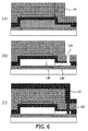
ステップ(f)にて、第2の電極122及び第1の誘電体層120を覆って、形成されるメンブレンの第2の誘電体層124が形成される。第2の誘電体層は典型的に、第2の電極の上方の第1の部分22と、第1の部分22から犠牲材料の第1の部分116に並んで且つ先述のように犠牲材料の第2の部分116’の間(及び上)で基板10の方に延在する第2の部分24とを有する。第1の部分22は初期厚さt1を有し、第2の部分は初期厚さw1を有し、w1及びt1は典型的に(おおよそ)等しい。誤解を避けるため、t1は図1におけるtに対応し、w1は図1におけるwに対応する。本発明の一実施形態によれば、図1の助けを借りて先述した比t/gを小さくするために、t1は第1の部分116の高さよりも大きく選定される。好適な一実施形態において、キャビティの形成中に望ましい頑強性をメンブレンに与えるために、比t/gは、4−20の範囲内、より好ましくは5−10の範囲内で選定される。例えば、犠牲部分116の高さgが100−700nmの範囲内で選定されるとともに、第1の部分22を犠牲部分116の少なくとも5倍の厚さにして、第1の部分22の厚さが0.5−10ミクロンの範囲内で選定される。
In step (f), a
第2の誘電体層124は、第1の誘電体層スタック120の少なくとも上側層と同じ材料で製造されることができ、一般には、例えば酸化シリコンや窒化シリコンといった好適な電気絶縁材料で製造されることができ、当然ながら、第2の誘電体層124が第1の誘電体層120とは相異なる材料で製造されることも実現可能である。しかしながら、その場合、キャビティを形成するために犠牲材料が除去される温度でそれらの層の間に熱誘起応力が構築されることを回避するために、それら相異なる材料それぞれの熱膨張係数が同等又は同じであるように注意を払うべきである。前述のように、第2の誘電体層124は如何なる好適手法で形成されてもよい。
The
ステップ(g)にて、第2の誘電体層124の第1の部分の上にエッチング停止層126が形成され、その後、犠牲材料の第2の部分116’へのアクセスを供するよう、第1の誘電体層120及び第2の誘電体層124を貫いて、アクセス又はビア128が形成される。これをステップ(h)に示す。アクセス又はビアは典型的に、先述のように、メンブレンの周縁の外側の犠牲材料の歯状の第2の部分116’のうちの1つ上に着地する。このようなアクセス又はビア128の形成それ自体は周知であり、単に簡潔さのために、更に詳細には説明しない。
In step (g), an
次に、ステップ(i)にて、CMUTデバイスのメンブレンの第1の誘電体層120と第2の誘電体層124との間に埋め込まれた第2の電極122と、第1の電極120との間にキャビティ130を形成するため、好適なエッチングレシピを用いて、アクセス又はビア128を通じて、犠牲材料の第1の部分116及び第2の部分116’が除去される。このような従来からの犠牲材料に関する好適なエッチングレシピそれ自体は周知であり、当業者は、自身の一般的常識を用いて、適切なエッチングレシピを困難なく選択するであろう。
Next, in step (i), the
その後、ステップ(j)にて、例えば好適な更なる誘電材料といった好適な封止材料を用いて、アクセス又はビア128が封止され、それにより、エッチング停止層126及び第2の誘電体層124を覆う更なる誘電材料層132と、アクセス又はビア128内の封止プラグ132’とが生み出される。一実施形態において、更なる誘電材料層132の最小厚さは、アクセス又はビア128の効果的な封止を確実にするため、キャビティ130の高さgの2倍である。この更なる誘電材料は、それ自体周知なような、何らかの好適な手法で堆積され得る何らかの好適な誘電材料とし得る。一実施形態において、この更なる誘電材料は、例えば酸化シリコン又は窒化シリコンなど、第2の誘電体層124の材料と同じ材料である。更なる誘電材料層132の形成は、第2の部分24によって定められるキャビティの壁部分の厚さを、ステップ(j)に示すようにw1+w2に増大させる。誤解を避けるために言及しておくに、w1+w2は図1におけるwに対応する。
Thereafter, in step (j), the access or via 128 is sealed using a suitable sealing material, such as a suitable additional dielectric material, thereby etching
CMUTデバイスの比t/wを小さくするため、ステップ(k)にて、第1の部分22の上方の更なる誘電材料層132の部分が、エッチング停止層126上で停止する例えば等方性ドライエッチングレシピといった好適なエッチングレシピを用いて、選択的に除去される。この時点で明らかなはずのことには、エッチング停止層の材料は、更なる誘電材料層132の選択部分を除去するのに使用されるエッチングレシピに対して高度に耐えるように選択される。そのような材料はそれ自体知られており、故に、如何なる好適なエッチング停止材料が選択されて如何なる好適な手法で堆積及びパターニングされてもよいと言えば十分である。
In order to reduce the CMUT device ratio t / w, in step (k), a portion of the further
その後、ステップ(k)にて、エッチング停止層が、例えばエッチングにより、開口134を形成するように除去されることで、第2の電極122の上方の第1の部分22の厚さがt1であり、且つキャビティ130の横に沿う第2の部分24の厚さがw1+w2である、すなわち、t1〜w1であるときにt1+w2であるメンブレンを有するCMUTデバイスが生み出される。従って、キャビティ130を形成するための犠牲材料の除去の段階でg≪t且つt≪wであるので、キャビティリリース工程中のメンブレン頑強性が向上されたCMUTデバイスが得られる。さらに、キャビティ130のリリースに先立って第2の誘電体層124が例えば堆積されて形成されるので、改善された平坦性を有するメンブレンが得られる。というのは、第2の誘電体層124の形成中に、犠牲材料の存在が第1の誘電体層120の変形を防止するからである。
Thereafter, in step (k), the etching stopper layer is removed by, for example, etching so as to form the
CMUTデバイスは更に、第2の部分24の上方に更なる誘電材料層132のリング136を有し、このリングが第1の部分22の境界を定める。見出されたことには、このようなリム(縁枠)又はリング構造(例えば兎の耳又はそれに類するような、先の尖った耳のような形状にされ得る)の存在は、キャビティリリース工程中のメンブレンの頑強さを更に高める。本願の文脈において、理解されるべきことには、頑強さは、図2に示したような面外変形‘h’に耐えるメンブレンの能力を記述するために使用される。
The CMUT device further includes a
しかしながら、このようなリング136は、他の実施形態におけるCMUTデバイス設計から省かれ得る。1つのそのような実施形態を、図4に示して上述した製造方法への選択された代替ステップを示すものである図5に示す。図5のステップ(a)は、図4のステップ(g)を置き換え、図5のステップ(b)は、図4のステップ(k)を置き換える。単に簡潔さのために図5には明示的に含めていないが、図4に示したその他のステップがまた、図5に描くプロセスフローの部分を形成する。
However, such a
ステップ(a)にて、エッチング停止層226は、第2の誘電体層124の第1の部分22及び第2の部分24を覆うような寸法にされる。これは、後続工程において、特に、図4のステップ(j)で形成される更なる誘電材料層132の選択的な除去において、第2の部分24の厚さが第1の部分22の厚さと比較して(有意に)増大されない、すなわち、この実施形態においてt〜wであるCMUTデバイスをもたらすという結果を有する。これは何故なら、更なる誘電材料層132の選択された部分を除去するエッチングレシピに対して、下に位置する第2の誘電体層124のいっそう大きい領域を保護するいっそう大きいエッチング停止層226から明らかになるように、第2の誘電体層124のいっそう広い領域の上で更なる誘電材料層132が除去されるからである。それに代えて、図5のステップ(b)に示すように、得られるCMUTデバイスは、アクセス又はビア128の中の封止プラグ132’と、この封止プラグから上方に延在する上記更なる誘電材料層の部分232とを有する。封止プラグ132’と部分232との組み合わせは、アクセス又はビア128に押し込まれるピンに例えられることができ、部分232がピンの頭部を形成する。分析式(1)から理解され得るように、図5(b)に示すCMUTデバイスはなおも、キャビティ130を形成するための犠牲材料の除去の段階でg≪tであるので、キャビティリリース工程中のメンブレン頑強さの向上を示す。さらに、キャビティ130のリリースに先立って第2の誘電体層124が例えば堆積されて形成されるので、改善された平坦性を有するメンブレンが得られる。というのは、第2の誘電体層124の形成中に、犠牲材料の存在が第1の誘電体層120の変形を防止するからである。
In step (a), the
一実施形態において、更なる誘電体層132は、例えばAl封止層などの金属の封止層によって置き換えられてもよい。これは、キャビティ130内の真空を改善する。というのは、金属は典型的に、気相で堆積されて高めの残留圧力をキャビティ130内に残すものである例えば窒化シリコンなどの誘電材料の堆積とは対照的に、高真空堆積技術を用いて堆積されるからである。従って、封止プラグ132’及び部分232は、例えばアルミニウムなどの好適な金属、又は例えばAl系合金といった金属合金で製造されてもよい。
In one embodiment, the additional
キャビティ130のリリースの時点で比g/t≪1を有するCMUTデバイス製造方法の他の一実施形態を図6に示す。図6の開始点は、図4のステップ(a)−(e)の後に得られた中間構造であり、すなわち、単に簡潔さのために図6には明示的に示していないが、図4に示したステップ(a)−(e)がまた、図6に示す製造方法の部分を形成する。
Another embodiment of a method for manufacturing a CMUT device having a ratio g / t << 1 at the time of release of the
第2の電極122の形成後、この方法は、図6のステップ(a)に示すように進み、第2の誘電体層124が、第1の電極112と第2の電極122との間の犠牲材料の第1の部分116の厚さを上回る第1の厚さt1’まで形成されることで、キャビティ130の形成後にキャビティ間隙の高さgが厚さt1’よりもかなり小さい、すなわち、g/t1’≪1であるようにされる。好ましくは、t1’≧5gである。これは、ステップ(b)でのキャビティ130のリリース中に、すなわち、図4のステップ(h)及び(i)にて更に詳細に記載した、アクセス又はビア128の形成とその後の犠牲材料の第1の部分116及び第2の部分116’の除去によるキャビティ130のリリース中に、キャビティリリース工程中にメンブレンがなおもメンブレン頑強さの向上を示すことを確実にする。というのは、キャビティ130を形成するための犠牲材料の除去の段階でg≪t1’であるからである。さらに、キャビティ130のリリースに先立って第2の誘電体層124が例えば堆積されて形成されるので、改善された平坦性を有するメンブレンが得られる。というのは、第2の誘電体層124の形成中に、犠牲材料の存在が第1の誘電体層120の変形を防止するからである。
After formation of the
図4及び5に示した方法とは対照的に、第2の誘電体層124上にエッチング停止層は形成されない。それに代えて、図4のステップ(j)の助けを借りて更に詳細に記載したアクセス又はビア128内のプラグ132’を含む更なる誘電体層132の形成によるステップ(c)でのアクセス又はビア128の封止において、メンブレンの厚さが更に増大される。一実施形態において、更なる誘電体層132は、第2の誘電体層124よりもかなり薄い。前述のように、更なる誘電体層132は、アクセス又はビア128を効果的に封止するためにキャビティ130の高さの少なくとも2倍の高さに形成される。これもやはり、図1に示したt及びwがおおよそ等しいCMUTデバイスを生み出す。というのは、第2の誘電体層124及び更なる誘電体層132は典型的にコンフォーマル(共形)に形成されるからである。
In contrast to the method shown in FIGS. 4 and 5, no etch stop layer is formed on the
この時点で言及しておくことには、図4−6それぞれの実施形態に従って形成されるCMUTデバイス群は、好ましくは、同じ又は同様の音響特性をデバイスが示すことを確保するよう、同じ最終メンブレン厚を有する。従って、第2の誘電体層124は典型的に、図6の実施形態と比較して、図4及び5の実施形態ではいっそう大きい厚さに形成される。というのは、図6に示した実施形態とは対照的に、封止層すなわち更なる誘電体層132が、キャビティ130を覆うメンブレンの少なくとも第1の部分22の最終厚さを追加しないからである。
It should be noted at this point that the CMUT device groups formed in accordance with the respective embodiments of FIGS. 4-6 preferably have the same final membrane to ensure that the devices exhibit the same or similar acoustic characteristics. Have a thickness. Accordingly, the
以上の実施形態は、例えば、50μm以上、特に100μm以上、例えば500若しくは更には1000μmに至るキャビティ半径を有するCMUTデバイスや、20−500μm、30−500μm、又は30−300μmの範囲内のキャビティ半径を有するデバイスなど、比較的大きいCMUTデバイスを、高い歩留りで作り出すことができることを例証している。というのは、キャビティ130の形成に先立って、第2の電極122の上方に厚い第2の誘電体層124を設けることによって、特にウェハの周縁部でのCMUTメンブレンの過度な変形が回避されたからである。
The above embodiments have a CMUT device having a cavity radius of, for example, 50 μm or more, in particular 100 μm or more, for example 500 or even 1000 μm, or a cavity radius in the range of 20-500 μm, 30-500 μm, or 30-300 μm. It illustrates that a relatively large CMUT device, such as a device having a high yield, can be created. This is because, by forming the thick second
この時点で言及しておくことには、リング形状とし得るものである本発明の実施形態に従ったCMUTデバイスは、例えば特許文献2(米国特許出願公開第2013/0069480号)の場合(特許文献2の特に図4A−F参照)のようにキャビティ130の形成後に第2の誘電体層124が形成される従来技術のデバイスから、容易に区別されることができる。これは何故なら、キャビティ130を形成するための犠牲材料の除去が、露出されたメンブレンの上面に残留汚染を形成させるからである(特許文献2のCMUTデバイスの場合、第1のメンブレン35上にそのような汚染の存在を生じさせることになる)。
It should be noted at this point that the CMUT device according to the embodiment of the present invention, which can be a ring shape, is, for example, in the case of Patent Document 2 (US Patent Application Publication No. 2013/0069480) (Patent Document). 2 can be easily distinguished from prior art devices in which the
対照的に、図4(k)、図5(b)及び図6(c)のCMUTデバイスでは、そのような汚染は、露出された第2の誘電材料層124の部分上に存在し、それ故に、キャビティ130を形成するための犠牲材料の除去中に第2の電極の上方にメンブレンの第2の誘電材料層124が存在していたかという事実を、そのような汚染の位置が指し示すことになる。換言すれば、メンブレンの下側領域における、すなわち、第1の誘電体層120表面上、又はキャビティ130に面し且つキャビティ130の間隙高さgに等しい厚さを持つメンブレンの領域内における、そのような汚染の不存在は、そのCMUTデバイスが本発明の製造方法の一実施形態に従って得られていることを指し示す。
In contrast, in the CMUT devices of FIGS. 4 (k), 5 (b), and 6 (c), such contamination is present on the exposed portion of the second
なお、そのような汚染は、メンブレンのそれぞれの誘電材料が例えば窒化シリコンといった同じ材料であるときでさえも、トンネル電子顕微鏡(TEM)イメージングを用いて検出されることができる。というのは、汚染物は、その後に堆積される同じ材料の層との間に明瞭な描写として現れるからである。 It should be noted that such contamination can be detected using tunneling electron microscope (TEM) imaging even when each dielectric material of the membrane is the same material, eg, silicon nitride. This is because contaminants appear as a clear depiction between layers of the same material that are subsequently deposited.
図4−6の実施形態の概念を、図7の助けを借りて更に説明する。図7はやはり、図3に示したような、比t/w(x軸)及びg/t(y軸)の関数としての第1のメンブレン部分22に関する変形プロットを描いている。描かれた変形特性は、分析式(1)を用いてモデル化される。従来技術のCMUTデバイスの変形特性にラベル700を付している。これらの特性における第1の向上が、図5及び6に示した方法に従って製造されるCMUTデバイスに関するg/t比の低減によって得られる(この特性にラベル710を付している)。これらの特性の更なる向上が、図4に示した方法に従って製造されるCMUTデバイスに関するg/t比及びt/w比の低減によって得られる(この特性にラベル720を付している)。
The concept of the embodiment of FIGS. 4-6 is further described with the help of FIG. FIG. 7 again depicts a deformation plot for the
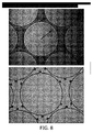
図8は、第2の電極上に厚い第2の誘電体層124が存在しない場合(上図)、及び図6に示した方法によって得られる第2の電極上に厚い第2の誘電体層124が存在する場合(下図)について、複数の円形のCMUTデバイスを有するウェハの、光学顕微鏡を用いて得られた像を示している。上図の平面内の矢印は、従来技術のCMUTデバイスのメンブレンにおける光リングを特定しており、これは、相当なメンブレン変形を指し示すものである。下図に光リングが存在しないことは、実施形態に従ったCMUTデバイスのメンブレンの、そのような変形に対する向上された頑強性を例証している。
FIG. 8 shows a thick second dielectric layer on the second electrode when there is no thick second
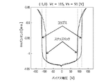
図9は、CMUTデバイスの典型的なキャパシタンス−電圧(CV)カーブを表している。増加していくバイアス電圧を第1の電極112と第2の電極122とにわたって印加すると、或る臨界電圧にて、電気力がメンブレンを第1の電極112の方に崩落(コラプス)させることになる。この電圧は、コラプス電圧としても知られている。電圧をコラプス電圧から低下させていくと、メンブレンはスナップバック電圧にてその元の位置へと跳ね返る(スナップバックする)ことになる。CMUTデバイスは、コラプスモード、すなわち、メンブレンがそのコラプス状態にあるモードで動作され得る。この目的のため、コラプス電圧を超えるバイアス電圧が、永続的に第1の電極112及び第2の電極122に印加され得る。
FIG. 9 represents a typical capacitance-voltage (CV) curve for a CMUT device. When an increasing bias voltage is applied across the
図2に示すようなメンブレン変形の量hは、コラプス電圧の大きさ及びCMUTデバイスの音響特性に顕著な影響を及ぼす。故に、ウェハにわたるCMUTデバイスのコラプス電圧のマッピングは、キャビティ形成中のCMUTデバイスの応力非感受性を指し示す良好なインジケーションを提供する。というのは、ウェハにわたるコラプス電圧の分布は、そのような応力非感受性の場合の小さい変化を例証するはずだからである。 The amount of membrane deformation h as shown in FIG. 2 has a significant effect on the magnitude of the collapse voltage and the acoustic characteristics of the CMUT device. Thus, the collapse voltage mapping of the CMUT device across the wafer provides a good indication of the stress insensitivity of the CMUT device during cavity formation. This is because the collapse voltage distribution across the wafer should illustrate such small changes in the case of such stress insensitivity.
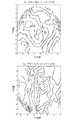
図10は、十分な厚さの第2の誘電体層124が存在せずにウェハにわたるCMUTデバイス群にそれぞれのキャビティ130が形成された図8の上図における、ウェハにわたるコラプス電圧Vcの等高線図を描いている。ウェハの中央では、およそ90VのVcの典型値が得られたが、ウェハの周縁では、この電圧が150V以上まで上昇しており、すなわち、このウェハは、ウェハにわたるCMUTデバイスのコラプス電圧Vcにおいて、65%を超えるバラつきを示している。これは、図2に示したようなメンブレンの面外屈曲を、ウェハ周縁において明瞭に指し示すものであり、この変形を逆にしてメンブレンをコラプスモードにさせるには、より高いバイアス電圧が必要である。
FIG. 10 is a contour plot of the collapse voltage Vc across the wafer in the upper view of FIG. 8 where each
図11は、本発明の異なる実施形態に従って製造された2つのウェハにわたるコラプス電圧Vcの等高線図を示している。上の等高線図は、図6の方法に従って製造されたウェハを示しており、下の等高線図は、図4の方法に従って製造されたウェハを示している。明らかなように、非常に小さいバラつき(7%未満のバラつき)のみが、ウェハの中央におけるCMUTデバイスのコラプス電圧Vcとウェハ周縁におけるCMUTデバイスのコラプス電圧Vcとの間に存在する。 FIG. 11 shows a contour plot of the collapse voltage Vc across two wafers manufactured according to different embodiments of the present invention. The upper contour plot shows a wafer manufactured according to the method of FIG. 6, and the lower contour plot shows a wafer manufactured according to the method of FIG. As is apparent, only very small variations (less than 7% variation) exist between the collapse voltage Vc of the CMUT device at the center of the wafer and the collapse voltage Vc of the CMUT device at the wafer periphery.
図12の上側の図は、図6の方法に従って製造されたウェハ上の位置(−4,0)から(0,+4)までの恣意的に選択されたCMUTデバイス(すなわち、ウェハの中心のCMUTデバイスを含む9個のCMUTデバイスのリニアアレイ)について、その出力圧の等高線図を示している。出力圧は、音響性能を指し示す重要なインジケータである。出力圧は、バイアス電圧(x軸)を−150Vから150Vまで変化させるとともにパルス長(y軸)を20nsから140nsまで変化させることにより、CMUTデバイスのRF励起によって生成した。下側の図は、これらのデバイスの各々の出力圧のヒストグラムを、ウェハ上でのそれらの位置の関数として示している。このアレイ内の全てのデバイスに関して、それらの出力圧における2%未満のバラつきを伴って、略等しい等高線図が得られた。これは、本発明の実施形態に従って製造されるウェハ上の(円形)CMUTデバイスの音響性能における優れた均一性を指し示すものである。 The upper diagram of FIG. 12 shows an arbitrarily selected CMUT device from position (−4,0) to (0, + 4) on the wafer manufactured according to the method of FIG. 9 shows a contour map of the output pressure of a linear array of nine CMUT devices including the device. Output pressure is an important indicator that indicates acoustic performance. The output pressure was generated by RF excitation of the CMUT device by changing the bias voltage (x axis) from −150 V to 150 V and changing the pulse length (y axis) from 20 ns to 140 ns. The lower diagram shows a histogram of the output pressure of each of these devices as a function of their position on the wafer. For all devices in this array, approximately equal contour plots were obtained with less than 2% variation in their output pressure. This indicates excellent uniformity in acoustic performance of (circular) CMUT devices on wafers manufactured according to embodiments of the present invention.
この時点で言及しておくに、様々な実施形態で図示されていないが、理解されるべきことには、実施形態に従って製造されるウェハ上のデバイスに従ったCMUTデバイスは、更なる回路要素を有していてもよく、それら更なる回路要素は、基板110上に集積されてもよいし、あるいは、別個の基板上に設けられて、本発明の実施形態に従って製造されたウェハからのCMUTデバイスのうちの1つ以上とともに単一のパッケージへと集積されてもよい。そのような更なる回路は例えば、先に説明したように例えば1つ以上のCMUTデバイスの送信及び/又は受信モードを制御するために、1つ以上のCMUTデバイスを制御し、且つ/或いは1つ以上のCMUTデバイスによって生成された信号を処理するための、例えばASICといったICとし得る。
It should be noted at this point that although not shown in various embodiments, it should be understood that a CMUT device according to a device on a wafer manufactured in accordance with the embodiment has additional circuit elements. These additional circuit elements may be integrated on the
本発明の実施形態に従った1つ以上のCMUTデバイスは、例えば圧力センシング装置などのセンシング装置に、特に、例えば超音波撮像装置といった医療撮像装置に、有利に組み込まれることができ、CMUTに基づくセンシング素子の集積は、装置の撮像分解能を有意に向上させることができる(これは例えば、人体などの哺乳類の体といった調査される被検体の体内の、例えば腫瘍などの異常といった小さいサイズの対象物の、検出可能性を向上させる)。一実施形態において、このような装置は、各CMUTデバイスが個々にアドレス指定可能であるマトリクスにて配置された、本発明の実施形態に従った複数のCMUTデバイスを有する。このような装置は、例えば、数百個又は数千個もの、このような個々にアドレス指定可能なCMUTデバイスを有し得る。 One or more CMUT devices according to embodiments of the present invention can be advantageously incorporated into sensing devices such as pressure sensing devices, in particular medical imaging devices such as ultrasound imaging devices, and are based on CMUTs. The integration of the sensing elements can significantly improve the imaging resolution of the device (for example, small objects such as abnormalities such as tumors in the body of the subject being examined, eg, a mammalian body such as a human body). Improve detectability). In one embodiment, such an apparatus has a plurality of CMUT devices according to an embodiment of the present invention arranged in a matrix in which each CMUT device is individually addressable. Such an apparatus may have, for example, hundreds or thousands of such individually addressable CMUT devices.
なお、上述の実施形態は、発明を限定ではなく例示するものであり、当業者は、添付の請求項の範囲を逸脱することなく、これらに代わる実施形態を設計することができるであろう。請求項において、括弧内に置かれた如何なる参照符号も、請求項を限定するものとして解されるべきでない。用語“有する”は、請求項に列挙されたもの以外の要素又はステップの存在を排除するものではない。要素の前に置かれた用語“a”又は“an”は、その要素が複数存在することを排除するものではない。本発明は、幾つかの異なる要素を有するハードウェアによって実装されることができる。複数の手段を列挙するデバイスの請求項において、それらの手段のうちの幾つかが同一のハードウェア品目で具現化されてもよい。特定の複数の手段が相互に異なる従属項に記載されているという単なる事実は、それらの手段の組合せが有利に使用され得ないということを指し示すものではない。 It should be noted that the above-described embodiments are illustrative rather than limiting, and those skilled in the art will be able to design alternative embodiments without departing from the scope of the appended claims. In the claims, any reference signs placed between parentheses shall not be construed as limiting the claim. The term “comprising” does not exclude the presence of elements or steps other than those listed in a claim. The term “a” or “an” preceding an element does not exclude the presence of a plurality of such elements. The present invention can be implemented by hardware having several different elements. In the device claim enumerating several means, several of these means may be embodied by one and the same item of hardware. The mere fact that certain measures are recited in mutually different dependent claims does not indicate that a combination of these measures cannot be used to advantage.
Claims (15)
前記メンブレン部分から前記封止部をエッチング除去することであり、前記エッチング停止層上で終了するエッチング除去することと、
前記エッチング除去する段階の後に、前記エッチング停止層を除去することと、
を更に有する請求項4に記載の方法。 Prior to the sealing step, forming an etch stop layer on the membrane portion;
Removing the sealing portion from the membrane portion by etching, and removing the etching that ends on the etching stop layer;
Removing the etch stop layer after the step of etching away;
The method of claim 4 further comprising:
前記犠牲材料を覆って第1の誘電材料層を形成し、
前記第1の誘電材料層上に第2の電極を形成し、且つ
前記第2の電極上に前記メンブレン部分を形成し、前記メンブレン部分は第2の誘電材料層の一部を形成する、
ことによって形成される、請求項1乃至6の何れかに記載の方法。 The membrane is at least partially
Forming a first dielectric material layer over the sacrificial material;
Forming a second electrode on the first dielectric material layer, and forming the membrane portion on the second electrode, the membrane portion forming part of a second dielectric material layer;
The method according to claim 1, wherein the method is formed by:
Applications Claiming Priority (3)
| Application Number | Priority Date | Filing Date | Title |
|---|---|---|---|
| EP13185792.2 | 2013-09-24 | ||
| EP13185792 | 2013-09-24 | ||
| PCT/EP2014/069574 WO2015043989A1 (en) | 2013-09-24 | 2014-09-15 | Cmut device manufacturing method, cmut device and apparatus |
Publications (2)
| Publication Number | Publication Date |
|---|---|
| JP2016540392A JP2016540392A (en) | 2016-12-22 |
| JP6416232B2 true JP6416232B2 (en) | 2018-10-31 |
Family
ID=49303731
Family Applications (1)
| Application Number | Title | Priority Date | Filing Date |
|---|---|---|---|
| JP2016516522A Active JP6416232B2 (en) | 2013-09-24 | 2014-09-15 | CMUT device manufacturing method, CMUT device, and apparatus |
Country Status (5)
| Country | Link |
|---|---|
| US (1) | US10293375B2 (en) |
| EP (1) | EP3049194B1 (en) |
| JP (1) | JP6416232B2 (en) |
| CN (1) | CN105592940B (en) |
| WO (1) | WO2015043989A1 (en) |
Families Citing this family (7)
| Publication number | Priority date | Publication date | Assignee | Title |
|---|---|---|---|---|
| US10722918B2 (en) | 2015-09-03 | 2020-07-28 | Qualcomm Incorporated | Release hole plus contact via for fine pitch ultrasound transducer integration |
| JP6461030B2 (en) * | 2016-03-15 | 2019-01-30 | 株式会社東芝 | Electronic device and method of manufacturing electronic device |
| EP4289521A3 (en) * | 2016-12-22 | 2024-03-27 | Koninklijke Philips N.V. | Systems and methods of operation of capacitive radio frequency micro-electromechanical switches |
| EP3533386A1 (en) * | 2018-02-28 | 2019-09-04 | Koninklijke Philips N.V. | Pressure sensing with capacitive pressure sensor |
| CN108871389B (en) * | 2018-05-10 | 2020-03-31 | 京东方科技集团股份有限公司 | Ultrasonic sensing unit, manufacturing method thereof, ultrasonic sensor and display device |
| TWI718073B (en) * | 2020-06-19 | 2021-02-01 | 友達光電股份有限公司 | Capacitive transducer and manufacturing method thereof |
| TWI813407B (en) * | 2022-08-02 | 2023-08-21 | 友達光電股份有限公司 | Capacitive transducer and manufacturing method thereof |
Family Cites Families (29)
| Publication number | Priority date | Publication date | Assignee | Title |
|---|---|---|---|---|
| JP2005207959A (en) * | 2004-01-26 | 2005-08-04 | Mitsubishi Electric Corp | Thin-film hollow structure |
| EP1713399A4 (en) * | 2004-02-06 | 2010-08-11 | Georgia Tech Res Inst | Cmut devices and fabrication methods |
| US8008835B2 (en) * | 2004-02-27 | 2011-08-30 | Georgia Tech Research Corporation | Multiple element electrode cMUT devices and fabrication methods |
| JP2008510324A (en) * | 2004-03-11 | 2008-04-03 | ジョージア テック リサーチ コーポレイション | Asymmetric thin film cMUT element and method of manufacturing |
| US20060004289A1 (en) * | 2004-06-30 | 2006-01-05 | Wei-Cheng Tian | High sensitivity capacitive micromachined ultrasound transducer |
| US8309428B2 (en) | 2004-09-15 | 2012-11-13 | Sonetics Ultrasound, Inc. | Capacitive micromachined ultrasonic transducer |
| US7888709B2 (en) | 2004-09-15 | 2011-02-15 | Sonetics Ultrasound, Inc. | Capacitive micromachined ultrasonic transducer and manufacturing method |
| US7489593B2 (en) * | 2004-11-30 | 2009-02-10 | Vermon | Electrostatic membranes for sensors, ultrasonic transducers incorporating such membranes, and manufacturing methods therefor |
| US7615834B2 (en) | 2006-02-28 | 2009-11-10 | The Board Of Trustees Of The Leland Stanford Junior University | Capacitive micromachined ultrasonic transducer(CMUT) with varying thickness membrane |
| JP2008213057A (en) * | 2007-03-01 | 2008-09-18 | Seiko Epson Corp | Vibrator structure and its manufacturing method |
| US20100256498A1 (en) * | 2007-11-16 | 2010-10-07 | Hiroki Tanaka | Ultrasonic imaging device |
| CN102159334A (en) * | 2008-09-16 | 2011-08-17 | 皇家飞利浦电子股份有限公司 | Capacitive micromachined ultrasound transducer |
| JP5851238B6 (en) * | 2009-03-05 | 2023-12-15 | 株式会社日立メディコ | Ultrasonic transducer, its manufacturing method, and ultrasonic probe using the same |
| US8760974B2 (en) * | 2009-04-21 | 2014-06-24 | Hitachi Medical Corporation | Ultrasonic probe and ultrasonic imaging apparatus |
| JP5377066B2 (en) * | 2009-05-08 | 2013-12-25 | キヤノン株式会社 | Capacitive electromechanical transducer and method for producing the same |
| CN101712028B (en) | 2009-11-13 | 2012-02-01 | 中国科学院声学研究所 | Thin-film ultrasonic transducer and preparation method thereof |
| JP5733898B2 (en) | 2010-02-14 | 2015-06-10 | キヤノン株式会社 | Capacitance type electromechanical transducer |
| JP5921079B2 (en) * | 2011-04-06 | 2016-05-24 | キヤノン株式会社 | Electromechanical transducer and method for manufacturing the same |
| JP5875243B2 (en) | 2011-04-06 | 2016-03-02 | キヤノン株式会社 | Electromechanical transducer and method for manufacturing the same |
| WO2013005486A1 (en) * | 2011-07-04 | 2013-01-10 | オリンパスメディカルシステムズ株式会社 | Electrostatic capacitance type ultrasonic transducer and electronic device |
| JP2013065983A (en) * | 2011-09-16 | 2013-04-11 | Canon Inc | Electromechanical conversion device and manufacturing method of the same |
| EP2806983B1 (en) * | 2012-01-27 | 2020-04-01 | Koninklijke Philips N.V. | Capacitive micro-machined transducer and method of manufacturing the same |
| BR112014018083A8 (en) * | 2012-01-27 | 2017-07-11 | Koninklijke Philips Nv | METHOD FOR MANUFACTURING A MICRO-MACHINING CAPACITIVE TRANSDUCER, IN PARTICULAR A CMUT AND MICRO-MACHINING CAPACITIVE TRANSDUCER, IN PARTICULAR A CMUT |
| JP5986441B2 (en) * | 2012-07-06 | 2016-09-06 | キヤノン株式会社 | Capacitive transducer |
| US9607606B2 (en) * | 2012-11-20 | 2017-03-28 | Koninkijke Philips N.V. | Capacitive micro-machined transducer and method of manufacturing the same |
| JP6257176B2 (en) * | 2013-06-07 | 2018-01-10 | キヤノン株式会社 | Capacitance type transducer and manufacturing method thereof |
| US9834434B2 (en) * | 2013-11-19 | 2017-12-05 | Canon Kabushiki Kaisha | Capacitive transducer and method of manufacturing the same |
| JP6320189B2 (en) * | 2014-06-18 | 2018-05-09 | キヤノン株式会社 | Capacitance type transducer and manufacturing method thereof |
| JP2016101417A (en) * | 2014-11-28 | 2016-06-02 | キヤノン株式会社 | Capacitance-type acoustic wave transducer and subject information acquisition apparatus with the same |
-
2014
- 2014-09-15 EP EP14766694.5A patent/EP3049194B1/en active Active
- 2014-09-15 CN CN201480052627.XA patent/CN105592940B/en active Active
- 2014-09-15 JP JP2016516522A patent/JP6416232B2/en active Active
- 2014-09-15 WO PCT/EP2014/069574 patent/WO2015043989A1/en active Application Filing
- 2014-09-15 US US15/021,962 patent/US10293375B2/en active Active
Also Published As
| Publication number | Publication date |
|---|---|
| JP2016540392A (en) | 2016-12-22 |
| US10293375B2 (en) | 2019-05-21 |
| US20160228915A1 (en) | 2016-08-11 |
| EP3049194B1 (en) | 2022-06-29 |
| CN105592940A (en) | 2016-05-18 |
| CN105592940B (en) | 2018-09-25 |
| EP3049194A1 (en) | 2016-08-03 |
| WO2015043989A1 (en) | 2015-04-02 |
Similar Documents
| Publication | Publication Date | Title |
|---|---|---|
| JP6416232B2 (en) | CMUT device manufacturing method, CMUT device, and apparatus | |
| JP6298216B2 (en) | Suspended membrane for capacitive pressure sensor | |
| US9938133B2 (en) | System and method for a comb-drive MEMS device | |
| US9611135B1 (en) | System and method for a differential comb drive MEMS | |
| TWI260940B (en) | Method for producing polymeric capacitive ultrasonic transducer | |
| JP2007528153A (en) | CMUT device and manufacturing method | |
| JP2015515609A (en) | Catheter die and manufacturing method thereof | |
| JP6422991B2 (en) | CMUT device and manufacturing method | |
| US10113928B2 (en) | Pressure sensor and a method for manufacturing the same | |
| CN105744388A (en) | Acoustic sensor and manufacturing method of the same | |
| JP4773630B2 (en) | Diaphragm type semiconductor device and manufacturing method thereof | |
| TW201306116A (en) | Method and device for preventing corrosion on sensors | |
| EP3682210B1 (en) | Capacitive pressure sensors and other devices having a suspended membrane and having rounded corners at an anchor edge | |
| US20130160554A1 (en) | Capacitive transducer manufacturing method, and multi-function device | |
| JP6185988B2 (en) | Wafer and manufacturing method thereof | |
| TW202043134A (en) | Method of manufacturing a semiconductor transducer device with multilayer diaphragm and semiconductor transducer device with multilayer diaphragm | |
| TW202029327A (en) | Semiconductor transducer device with multilayer diaphragm and method of manufacturing a semiconductor transducer device with multilayer diaphragm | |
| JP2015213224A (en) | Manufacturing method of capacitive transducer, and capacitive transducer |
Legal Events
| Date | Code | Title | Description |
|---|---|---|---|
| A621 | Written request for application examination |
Free format text: JAPANESE INTERMEDIATE CODE: A621 Effective date: 20170912 |
|
| A977 | Report on retrieval |
Free format text: JAPANESE INTERMEDIATE CODE: A971007 Effective date: 20180813 |
|
| TRDD | Decision of grant or rejection written | ||
| A01 | Written decision to grant a patent or to grant a registration (utility model) |
Free format text: JAPANESE INTERMEDIATE CODE: A01 Effective date: 20180904 |
|
| A61 | First payment of annual fees (during grant procedure) |
Free format text: JAPANESE INTERMEDIATE CODE: A61 Effective date: 20181003 |
|
| R150 | Certificate of patent or registration of utility model |
Ref document number: 6416232 Country of ref document: JP Free format text: JAPANESE INTERMEDIATE CODE: R150 |
|
| R250 | Receipt of annual fees |
Free format text: JAPANESE INTERMEDIATE CODE: R250 |
|
| R250 | Receipt of annual fees |
Free format text: JAPANESE INTERMEDIATE CODE: R250 |
|
| R250 | Receipt of annual fees |
Free format text: JAPANESE INTERMEDIATE CODE: R250 |