JP6416196B2 - Combination of steering antenna, CPL antenna, and one or more logarithmic detection amplifiers for reception - Google Patents
Combination of steering antenna, CPL antenna, and one or more logarithmic detection amplifiers for reception Download PDFInfo
- Publication number
- JP6416196B2 JP6416196B2 JP2016503241A JP2016503241A JP6416196B2 JP 6416196 B2 JP6416196 B2 JP 6416196B2 JP 2016503241 A JP2016503241 A JP 2016503241A JP 2016503241 A JP2016503241 A JP 2016503241A JP 6416196 B2 JP6416196 B2 JP 6416196B2
- Authority
- JP
- Japan
- Prior art keywords
- lda
- antenna
- frequency
- output
- signal
- Prior art date
- Legal status (The legal status is an assumption and is not a legal conclusion. Google has not performed a legal analysis and makes no representation as to the accuracy of the status listed.)
- Active
Links
Images


Classifications
-
- H—ELECTRICITY
- H04—ELECTRIC COMMUNICATION TECHNIQUE
- H04B—TRANSMISSION
- H04B1/00—Details of transmission systems, not covered by a single one of groups H04B3/00 - H04B13/00; Details of transmission systems not characterised by the medium used for transmission
- H04B1/02—Transmitters
- H04B1/04—Circuits
- H04B1/0475—Circuits with means for limiting noise, interference or distortion
-
- H—ELECTRICITY
- H01—ELECTRIC ELEMENTS
- H01Q—ANTENNAS, i.e. RADIO AERIALS
- H01Q21/00—Antenna arrays or systems
- H01Q21/28—Combinations of substantially independent non-interacting antenna units or systems
-
- H—ELECTRICITY
- H01—ELECTRIC ELEMENTS
- H01Q—ANTENNAS, i.e. RADIO AERIALS
- H01Q3/00—Arrangements for changing or varying the orientation or the shape of the directional pattern of the waves radiated from an antenna or antenna system
- H01Q3/24—Arrangements for changing or varying the orientation or the shape of the directional pattern of the waves radiated from an antenna or antenna system varying the orientation by switching energy from one active radiating element to another, e.g. for beam switching
-
- H—ELECTRICITY
- H01—ELECTRIC ELEMENTS
- H01Q—ANTENNAS, i.e. RADIO AERIALS
- H01Q3/00—Arrangements for changing or varying the orientation or the shape of the directional pattern of the waves radiated from an antenna or antenna system
- H01Q3/26—Arrangements for changing or varying the orientation or the shape of the directional pattern of the waves radiated from an antenna or antenna system varying the relative phase or relative amplitude of energisation between two or more active radiating elements; varying the distribution of energy across a radiating aperture
- H01Q3/30—Arrangements for changing or varying the orientation or the shape of the directional pattern of the waves radiated from an antenna or antenna system varying the relative phase or relative amplitude of energisation between two or more active radiating elements; varying the distribution of energy across a radiating aperture varying the relative phase between the radiating elements of an array
- H01Q3/34—Arrangements for changing or varying the orientation or the shape of the directional pattern of the waves radiated from an antenna or antenna system varying the relative phase or relative amplitude of energisation between two or more active radiating elements; varying the distribution of energy across a radiating aperture varying the relative phase between the radiating elements of an array by electrical means
- H01Q3/36—Arrangements for changing or varying the orientation or the shape of the directional pattern of the waves radiated from an antenna or antenna system varying the relative phase or relative amplitude of energisation between two or more active radiating elements; varying the distribution of energy across a radiating aperture varying the relative phase between the radiating elements of an array by electrical means with variable phase-shifters
-
- H—ELECTRICITY
- H01—ELECTRIC ELEMENTS
- H01Q—ANTENNAS, i.e. RADIO AERIALS
- H01Q7/00—Loop antennas with a substantially uniform current distribution around the loop and having a directional radiation pattern in a plane perpendicular to the plane of the loop
-
- H—ELECTRICITY
- H01—ELECTRIC ELEMENTS
- H01Q—ANTENNAS, i.e. RADIO AERIALS
- H01Q9/00—Electrically-short antennas having dimensions not more than twice the operating wavelength and consisting of conductive active radiating elements
- H01Q9/04—Resonant antennas
- H01Q9/30—Resonant antennas with feed to end of elongated active element, e.g. unipole
- H01Q9/42—Resonant antennas with feed to end of elongated active element, e.g. unipole with folded element, the folded parts being spaced apart a small fraction of the operating wavelength
-
- H—ELECTRICITY
- H03—ELECTRONIC CIRCUITRY
- H03F—AMPLIFIERS
- H03F3/00—Amplifiers with only discharge tubes or only semiconductor devices as amplifying elements
- H03F3/20—Power amplifiers, e.g. Class B amplifiers, Class C amplifiers
- H03F3/24—Power amplifiers, e.g. Class B amplifiers, Class C amplifiers of transmitter output stages
-
- H—ELECTRICITY
- H04—ELECTRIC COMMUNICATION TECHNIQUE
- H04B—TRANSMISSION
- H04B1/00—Details of transmission systems, not covered by a single one of groups H04B3/00 - H04B13/00; Details of transmission systems not characterised by the medium used for transmission
- H04B1/06—Receivers
- H04B1/16—Circuits
- H04B1/18—Input circuits, e.g. for coupling to an antenna or a transmission line
-
- H—ELECTRICITY
- H04—ELECTRIC COMMUNICATION TECHNIQUE
- H04B—TRANSMISSION
- H04B1/00—Details of transmission systems, not covered by a single one of groups H04B3/00 - H04B13/00; Details of transmission systems not characterised by the medium used for transmission
- H04B1/38—Transceivers, i.e. devices in which transmitter and receiver form a structural unit and in which at least one part is used for functions of transmitting and receiving
- H04B1/40—Circuits
- H04B1/50—Circuits using different frequencies for the two directions of communication
- H04B1/52—Hybrid arrangements, i.e. arrangements for transition from single-path two-direction transmission to single-direction transmission on each of two paths or vice versa
- H04B1/525—Hybrid arrangements, i.e. arrangements for transition from single-path two-direction transmission to single-direction transmission on each of two paths or vice versa with means for reducing leakage of transmitter signal into the receiver
-
- H—ELECTRICITY
- H04—ELECTRIC COMMUNICATION TECHNIQUE
- H04B—TRANSMISSION
- H04B1/00—Details of transmission systems, not covered by a single one of groups H04B3/00 - H04B13/00; Details of transmission systems not characterised by the medium used for transmission
- H04B1/02—Transmitters
- H04B1/04—Circuits
- H04B2001/0408—Circuits with power amplifiers
Landscapes
- Engineering & Computer Science (AREA)
- Computer Networks & Wireless Communication (AREA)
- Signal Processing (AREA)
- Power Engineering (AREA)
- Transceivers (AREA)
- Variable-Direction Aerials And Aerial Arrays (AREA)
- Amplifiers (AREA)
- Mobile Radio Communication Systems (AREA)
- Details Of Aerials (AREA)
Description
この出願は、2013年3月15日に提出された米国仮出願61/798,521、および2014年3月14日に提出された米国特許出願14/214,579の利益を請求する。 This application claims the benefit of US Provisional Application 61 / 798,521, filed March 15, 2013, and US Patent Application 14 / 214,579, filed March 14, 2014.
本発明は、無線および有線モードにおける混信をなくすためのいくつかの方法および対数検波増幅器(LDA)の実施に関する。そのような方法は、MIMO上の多数のアンテナの選択、調節および操縦と同様に、受信器性能を改善するために、受信アンテナ当たり1つのLDAが、ステアリングあるいはCPLアンテナと共に使用される方法とを含んでいる。本発明の庇護の下に、部分的組み合わせが含まれる。1つは、新しい高性能高集積RFフロントエンドにおいて、1つ以上のLDAを利用して、より限定的に実施形態を取り扱うもの、もう1つは、送信電力増幅器としてのLDAを含む、LDAの双方向用途について述べるもの、および最後に、LDAおよびアクティブアンテナの集積トポロジーである。 The present invention relates to several methods and logarithmic detection amplifier (LDA) implementations for eliminating interference in wireless and wired modes. Such a method describes how one LDA per receive antenna can be used with a steering or CPL antenna to improve receiver performance, as well as the selection, adjustment and steering of multiple antennas over MIMO. Contains. Partial combinations are included under the protection of the present invention. One that deals with embodiments more restrictively in one or more new high-performance highly integrated RF front ends, using one or more LDAs, and the other includes LDAs as transmit power amplifiers. What describes bidirectional applications, and finally, is an integrated topology of LDA and active antennas.
携帯電話および他の無線通信デバイスの新しい世代は、より小型化するとともに増加したアプリケーションが埋め込まれており、新しいアンテナ・デザインはこれらの装置の固有の制限に取り組むこと、および新しい性能を可能にすることが要求される。従来のアンテナ構造では、ある物理的容積が、特定周波数および特定帯域幅での共振アンテナ構造を生成するために要求される。しかしながら、そのようなアンテナの有効な実装は、しばしば装置中の制限された利用可能空間によるサイズ制約に直面している。 New generations of mobile phones and other wireless communication devices are becoming smaller and embedded with increased applications, and new antenna designs address the inherent limitations of these devices and enable new performance Is required. In conventional antenna structures, some physical volume is required to create a resonant antenna structure with a specific frequency and a specific bandwidth. However, effective implementations of such antennas often face size constraints due to limited available space in the device.
アンテナ能率は、装置の性能を決定する重要なパラメーターのうちの1つである。詳しくは、放射効率は、放射がどれくらい有効に生じるかを述べる物理量であり、放射されたパワーとアンテナの入力パワーの比率として表現される。より効率的なアンテナは、それに供給されたエネルギーをより高い比率で放射するであろう。同様に、アンテナの固有の相互性により、より効率的なアンテナは受信エネルギーのより多くを電気エネルギーに変換するであろう。したがって、よい効率およびコンパクトなサイズの両方を有するアンテナは、種々様々のアプリケーションのためにしばしば望まれる。 Antenna efficiency is one of the important parameters that determine device performance. Specifically, the radiation efficiency is a physical quantity that describes how effectively radiation is generated, and is expressed as a ratio between the radiated power and the input power of the antenna. A more efficient antenna will radiate the energy supplied to it at a higher rate. Similarly, due to the inherent reciprocity of antennas, a more efficient antenna will convert more of the received energy into electrical energy. Thus, antennas with both good efficiency and compact size are often desired for a wide variety of applications.
従来のループアンテナは典型的に電流が供給される装置である。それは磁場(H)を最初に生成する。そのため、それらは、トランスミッタとして典型的に適切ではない。これは、小さなループアンテナに特に該当する。(つまり、1波長より小さい、あるいはそれ未満の直径である)。ループアンテナによって受け取られた放射エネルギーの量の一部は、その領域によって決定される。典型的には、ループの領域が半分にされるごとに、受信可能なエネルギー量はおよそ3dB低減される。したがって、サイズと効率の釣り合いはループアンテナ・デザインに対する主要な検討事項の1つである。 Conventional loop antennas are devices that are typically supplied with current. It first generates a magnetic field (H). As such, they are typically not suitable as transmitters. This is especially true for small loop antennas. (In other words, the diameter is less than or equal to one wavelength.) Part of the amount of radiant energy received by the loop antenna is determined by the area. Typically, each time the loop area is halved, the amount of receivable energy is reduced by approximately 3 dB. Therefore, the balance between size and efficiency is one of the major considerations for loop antenna design.
ダイポールのような電圧供給アンテナは電場(E)および磁場Hの両方を放射し、送信および受信モードの両方で使用することができる。複合アンテナは、直交磁場(TM)および直交電場(TE)モードが励起されるものであり、たとえば広い帯域幅(低いQ)、大きな放射強度/力/利得および高効率などの性能利点に帰着する。2次元の非複合のアンテナの多くの例があり、一般に回路基板上の金属の印刷された線条を含んでいる。これらアンテナの大部分は電圧が供給される。1のそのようなアンテナの一例は、平面逆F型アンテナ(PIFA)である。多くのアンテナ・デザインは、4分の1波長(あるいは波長の4分の1のある倍数)、電圧供給、ダイポールアンテナを利用する。 A voltage supply antenna such as a dipole radiates both an electric field (E) and a magnetic field H and can be used in both transmit and receive modes. A composite antenna is one in which orthogonal magnetic field (TM) and orthogonal electric field (TE) modes are excited, resulting in performance advantages such as wide bandwidth (low Q), large radiation strength / force / gain and high efficiency. . There are many examples of two-dimensional non-composite antennas, typically including printed metal strips on a circuit board. Most of these antennas are supplied with voltage. An example of one such antenna is a planar inverted-F antenna (PIFA). Many antenna designs utilize a quarter wavelength (or a multiple of a quarter of a wavelength), a voltage supply, and a dipole antenna.
エラー率を最小化する一方で増強されたデータ通信比率を提供するために、MIMO(複数入力複数出力)技術の使用が、今日の無線通信デバイスの中で増加している。MIMOシステムは、同一ではないが同じメッセージの異なる変形である異なる信号を送信するためにいくつかの送信(Tx)アンテナと、異なる信号を同時に受信するいくつかの受信(Rx)アンテナとを同時に使用することにより、多重通路伝送の環境からの干渉を緩和することを目指している、MIMOシステムは一般に、アレイ利得を達成するように同じ合計送信電力をアンテナに広げることによって、補足帯域幅あるいは増加した送信電力なしで、データ・スループットの著しい増加を提示することができる。MIMOプロトコルは、IEEE802.11n(Wi−Fi)、4G、ロングタームエボリューション(LTE)、WiMAXおよびHSPA+などのような無線通信規格の一部を構成する。しかしながら、複数アンテナを備える構成では、サイズ制約は、厳しくなる傾向がある。また、アンテナ中の電磁結合によって引き起こされた干渉効果は、著しく送信および受信品質の質を下げるかもしれない。同時に、効率は、多重経路がエネルギーを与えられ、電源消費が増加するという多くの実例の中で、低下する可能性がある。 The use of MIMO (multiple input multiple output) technology is increasing among today's wireless communication devices to provide an increased data communication rate while minimizing error rates. A MIMO system uses several transmit (Tx) antennas simultaneously and several receive (Rx) antennas that receive different signals simultaneously to transmit different signals that are not the same but are different variants of the same message. By aiming to mitigate interference from the multipath transmission environment, MIMO systems generally gain supplemental bandwidth or increased by spreading the same total transmit power to the antenna to achieve array gain A significant increase in data throughput can be presented without transmission power. The MIMO protocol forms part of wireless communication standards such as IEEE 802.11n (Wi-Fi), 4G, Long Term Evolution (LTE), WiMAX, and HSPA +. However, in a configuration including a plurality of antennas, the size constraint tends to be severe. Also, interference effects caused by electromagnetic coupling in the antenna may significantly reduce the quality of transmission and reception quality. At the same time, efficiency can be reduced in many instances where multiple paths are energized and power consumption increases.
送信および受信品質でのそのような低下は、WLANおよびWANアプリケーションの有効範囲、任意の時点で与えられる実効スループット、および干渉レベルには特に問題であり、キャパシティーは、有効な広帯域の接続性に、特に重要なパラメーターである。普段のビデオストリーミングのような新しいアプリケーションを備えた、WLANおよびWANのための性能性期待は、非常に高く、そのようなシステムの中で使用されるアンテナは、パフォーマンスを改善するためにこれらのパフォーマンス問題に対処することができなければならない。 Such degradation in transmission and reception quality is particularly problematic for the coverage of WLAN and WAN applications, the effective throughput given at any point in time, and the level of interference, and capacity is limited to effective broadband connectivity. Is a particularly important parameter. The performance expectations for WLANs and WANs with new applications such as regular video streaming are very high, and the antennas used in such systems are subject to these performances to improve performance. You must be able to deal with the problem.
エンド・ユーザによって経験されるようなスマートフォンに備えたWAN、またはPCか携帯型のデバイスに備えた個人的または公衆のWLANネットワークの上で、パフォーマンスを改善する多くの機会がある。具体的には、各住居がそれぞれ1つ以上のWi−Fiアクセス・ポイントまたはルーターがあるところで、WLANは、住宅のシナリオにおける住宅の配備に改良の余地を持っている。通信圏および区域でのスループットは、この数年にわたって劇的に進歩し、平均では、大多数のユーザはよい通信圏と全体にわたるデータとを家庭内で得て居る。しかしながら増加している問題は、毎年増加する利用可能な帯域幅の不足および関連する干渉問題である。WLAN使用のための最初のISMバンドはアメリカで900MHzだった。カメラおよびコードレス電話機のようなデバイス、および様々なプロトコルおよび異なる変調スキームの存在によって、900MHzのバンドは、急速に混雑するようになった。その後、2.4GHz帯が割り当てられ、11のチャネル上のIEEE 802.11bおよび802.11gデバイスが使用されたが、オーバーラップしないチャネルは3つだけであった。 There are many opportunities to improve performance on WANs with smartphones as experienced by end users, or on personal or public WLAN networks with PCs or portable devices. Specifically, where each residence has one or more Wi-Fi access points or routers, WLANs have room for improvement in housing deployment in residential scenarios. Throughput over the service area and area has improved dramatically over the last few years, and on average, the majority of users have a good service area and overall data at home. However, an increasing problem is the lack of available bandwidth and associated interference problems that increase year by year. The first ISM band for WLAN use was 900 MHz in the United States. With the presence of devices such as cameras and cordless phones, and various protocols and different modulation schemes, the 900 MHz band became rapidly crowded. Later, the 2.4 GHz band was allocated and IEEE 802.11b and 802.11g devices on 11 channels were used, but only 3 channels did not overlap.
新しいコードレス電話機(たとえばデジタル増強コードレス電気通信 DECT6.0)も2.4GHz帯に導入され、現状では、平均で、任意の大都市圏または郊外において、WLANノードはそれぞれ近辺で5つまたは10のルーターに出会う。ルーターにとって、それらは互いに悪者アプリケーションとして見るので、それは帯域幅のための競争を意味する。送信電力を減少させるための、および後退(遅延)送信のアルゴリズムが存在する。しかし、実際的な側で、それらはWi−Fiアプリケーションであまり頻繁には適用されない。LTE、WCDMAのためにだが、携帯用ハンドセットユーザ設備(UE)、発展したノードB(enodeB)、およびGSM中のベーストランシーバ局との間の一定電力調節がある。平均では、2.4GHz帯も混雑する。比較的5GHz帯の新用途はよりもっとオーバーラップしないチャネルを提供するが、しかしより高い解像度のより多くのビデオに対する必要性によって悪化した、より多くの帯域幅に対する絶え間がない切望は、160MHzの帯域幅での802.11acのような、より多くの帯域幅リソースの必要を示唆する。 New cordless telephones (eg, digital enhanced cordless telecommunications DECT 6.0) have also been introduced in the 2.4 GHz band, and currently, on average, in any metropolitan area or suburb, each WLAN node has 5 or 10 routers in the vicinity. Meet. For routers, they see each other as bad applications, so that means competition for bandwidth. There are algorithms for reducing transmit power and for backward (delayed) transmission. However, on the practical side, they are not applied very often in Wi-Fi applications. For LTE, WCDMA, there is a constant power adjustment between the portable handset user equipment (UE), the evolved Node B (enodeB), and the base transceiver station in GSM. On average, the 2.4 GHz band is also crowded. New applications in the relatively 5 GHz band provide more non-overlapping channels, but the constant desire for more bandwidth, exacerbated by the need for more video with higher resolution, is the 160 MHz band It suggests the need for more bandwidth resources, such as 802.11ac in width.
WLANとWANのシステムに関する性能上の問題は全般的に新世代の802.11b/g/a/n無線カードおよびモジュールの開発によって、対処された。しかしながら、近くの無線LANは、大部分が、チャネルをオーバーラップさせる干渉取り消しによって、互いに競合する。この競合は、クライアントがルーターからより遠くなるほど、および近隣のWLANの中の競い合うルーターへ近づくほど帯域幅を低減する。さらに干渉によるビデオアプリケーション用の弱いスループット・データまたは能力不足が問題を残し、パフォーマンス向上のための主な機会を提供する。さらに、現在の802.11システムは、橋架けモードによって、セルラー装置、タブレットおよびPCに、ダウンロード(DL)でのデータの3Gbpsまで、およびアップロード(UL)での1.5Gbpsまでを約束するLTEアドバンストリリース10(http://www.3gpp.org)のような、新しい競い合う無線基準と比較されるに違いない。主な違いは、住宅環境内のLTE対Wi−Fiのような、セルラー・ネットワークの同期態様である。干渉問題は存在せず、LTE対Wi−Fiであまり低速であるべきでない;しかしながら、完全な容量および低スループットが、マルチパスフェージングによって、同期されたWANに対してさえまだ存在する。 Performance issues related to WLAN and WAN systems were generally addressed by the development of new generation 802.11b / g / a / n wireless cards and modules. However, nearby wireless LANs mostly compete with each other due to interference cancellation that causes the channels to overlap. This contention reduces bandwidth as the client is further away from the router and closer to competing routers in neighboring WLANs. In addition, weak throughput data or lack of capacity for video applications due to interference leaves problems and provides a major opportunity for performance improvement. In addition, the current 802.11 system is LTE advanced, which promises up to 3 Gbps of data in download (DL) and 1.5 Gbps in upload (UL) to cellular devices, tablets and PCs via bridge mode. It must be compared to new competing radio standards, such as Release 10 (http://www.3gpp.org). The main difference is the manner in which cellular networks are synchronized, such as LTE vs. Wi-Fi in a residential environment. There are no interference problems and should not be too slow with LTE vs. Wi-Fi; however, full capacity and low throughput still exist for even synchronized WANs due to multipath fading.
本出願人は、レシーバーが、ノイズがある状態で下位レベル・システムをより確実に受信することを可能にすることにより、上記の問題に対処する対数検波増幅器(LDA)を開発した。さらに、LDAは、付近のデバイスとのより低レベルの干渉を提供するために、送信器の送信出力が比例的に減少することを可能にする。典型的なLDAはUS特許7,911,235に述べられている。その内容は、参照によって、本明細書に組み込まれる。そこに説明されたように、LDAは、増幅器(例えば離散的なトランジスタまたは演算増幅器)、検出器の動作周波数をセットするための手段(例えば、同調されたL−CまたはR−C帰還回路またはフェーズロックループ)、およびコントローラを含む。増幅器への入力信号は、増幅器の発振を引き起こし、コントローラは発振を指示するしきい値を感知し、発振の検知に応答して、中断周波数が入力信号の出力の対数に比例するようにして、増幅器の発振を中断する。 Applicants have developed a logarithmic detector amplifier (LDA) that addresses the above problem by allowing the receiver to more reliably receive lower level systems in the presence of noise. In addition, LDA allows the transmitter's transmit power to be proportionally reduced to provide lower levels of interference with nearby devices. A typical LDA is described in US Pat. No. 7,911,235. The contents of which are hereby incorporated by reference. As described therein, an LDA is an amplifier (eg, a discrete transistor or operational amplifier), a means for setting the operating frequency of a detector (eg, a tuned LC or RC feedback circuit or Phase lock loop), and controller. The input signal to the amplifier causes the amplifier to oscillate, and the controller senses a threshold value indicating oscillation, and in response to detecting the oscillation, the interrupt frequency is proportional to the logarithm of the output of the input signal, Suspends amplifier oscillation.
オペレーションの間、増幅器の入力の電気雑音は、L−C調整された帰還回路によって測定された周波数で回路の発振をセット・アップする。同調回路の帯域幅外の雑音は、回路のオペレーションに最小の影響を持つ。他方、L−C同調帰還回路の帯域幅内に位置する入力信号は、ランダムノイズだけが回路を励起していた場合よりも、発振器をより高速に振動させる。受信されるノイズ中で求められる信号がある場合、オペレーションの設定周波数での入力信号の相対レベルは高く、しきい値は、ランダムノイズだけのための場合よりも早く到達するだろう。求められる信号のレベルが高いほど、しきい値はより早く到達し、発振の中断はより頻繁になる。従って、所要の周波数を持っている求められる信号は、ランダムノイズだけより発振をより速く生じさせる。そのようなLDAは、干渉をキャンセルするのに全く効果的であることが示された。 During operation, the electrical noise at the input of the amplifier sets up the circuit's oscillation at the frequency measured by the L-C tuned feedback circuit. Noise outside the bandwidth of the tuning circuit has minimal impact on the operation of the circuit. On the other hand, an input signal located within the bandwidth of the L-C tuned feedback circuit causes the oscillator to oscillate faster than if only random noise was exciting the circuit. If there is a desired signal in the received noise, the relative level of the input signal at the set frequency of operation will be high and the threshold will be reached sooner than for random noise alone. The higher the required signal level, the faster the threshold is reached and the more frequent the oscillation breaks. Thus, the required signal having the required frequency will oscillate faster than only random noise. Such an LDA has been shown to be quite effective at canceling interference.
より大きな空間的多様性の提供により、技術上の前述の問題に対処することが望まれる。
従来のモバイルのセルラー・ネットワーク・システムでは、基地局にはセル内のモバイルユニットの位置についての情報はなく、無線通信圏を提供するために、セル内にあらゆる方向の信号を放射する。これは、到達するモバイルユニットがない場合、いわゆる同一チャネルセルと呼ばれる、同じ周波数を使用する隣接セルとの干渉を引き起こすことに加えて、送信中の電力の浪費との結果となる。同様に、受信においでは、アンテナは、ノイズおよび干渉信号を含む、すべての方向から来る信号を受け取る。スマートアンテナ技術の使用によって、およびセル内のモバイルユニットの空間的配置を異ならせることによって、空間分割多元接続技術は、魅力的なパフォーマンス強化を提供する。基地局の放射パターンは、送信と受信の両方で、そのユーザの方向に最も高い利得を得るために各ユーザに適応させる。これはフェーズドアレイ技術を使用して、頻繁に行われる。
It would be desirable to address the aforementioned technical problems by providing greater spatial diversity.
In a conventional mobile cellular network system, the base station has no information about the location of the mobile unit in the cell and radiates signals in all directions in the cell to provide a wireless communication range. This results in wasted power during transmission in addition to causing interference with neighboring cells using the same frequency, called so-called co-channel cells, when there are no mobile units to reach. Similarly, at reception, the antenna receives signals coming from all directions, including noise and interference signals. Spatial division multiple access technology offers attractive performance enhancements through the use of smart antenna technology and by varying the spatial arrangement of mobile units within a cell. The base station radiation pattern is adapted to each user to obtain the highest gain in the direction of that user, both in transmission and reception. This is often done using phased array technology.
そのようなアンテナを使用する、増加した空間の多様性、およびLDAを使用する場合の干渉取り消しにおける著しい改良の観点から、無線および有線の通信を利用する通信の新しいアプリケーションにおいて、本発明に従ってLDAの使用を探求することが要望される。特に、干渉を低減するか除去するために、LDA、複数のアンテナ、アクティブアンテナ、および複数のアクティブアンテナおよびレシーバーを同期させ、それによって、無線ルーターとそれらのクライアントの間でより大きな範囲および帯域幅を提供することが特に望まれる。本発明は、これらの及び他の技術分野の必要性に対処する。 In view of the increased spatial diversity using such antennas and the significant improvement in interference cancellation when using LDA, LDA's in accordance with the present invention in new applications of communication utilizing wireless and wired communications. It is desired to explore use. In particular, synchronize LDA, multiple antennas, active antennas, and multiple active antennas and receivers to reduce or eliminate interference, thereby providing greater range and bandwidth between wireless routers and their clients It is particularly desirable to provide The present invention addresses these and other technical needs.
請求されたアンテナシステムは、無線通信での干渉を低減するか実質的に除去するために適合させたLDAを用いて、空間多様性を改善するために適合させたアンテナを含む1つ以上の解決手段の実施によって、前述の技術的要求に対処する。上で言及したように、近くの無線LANは、大部分がオーバーラッピングチャンネルの干渉取り消しによって、互いと競合する。クライアントがルーターからより遠くなり、付近のWLANの競い合うルーターにより近くなるほど、この競合は帯域幅を低減する。この取り消しを低減するか除去するために同期された、LDA、複数のアンテナ、アクティブアンテナおよび複数のアクティブアンテナおよびレシーバーの使用を通じ、ここに記述されるような本発明を使用する、無線ルーターとそれらのクライアントの間のより広い範囲および帯域幅が提供できるかもしれない。 The claimed antenna system uses one or more solutions that include antennas adapted to improve spatial diversity using LDA adapted to reduce or substantially eliminate interference in wireless communications. The implementation of the means addresses the aforementioned technical requirements. As mentioned above, nearby wireless LANs compete with each other, mostly due to interference cancellation of overlapping channels. As the client is further away from the router and closer to the neighboring WLAN competing router, this contention reduces the bandwidth. Wireless routers and those using the present invention as described herein through the use of synchronized LDA, multiple antennas, active antennas and multiple active antennas and receivers to reduce or eliminate this cancellation A wider range and bandwidth between clients may be able to provide.
本明細書に記述された本発明は、干渉のこの問題に取り組み、干渉を一部分または全部低減するために、LDA、複数のアンテナ、アクティブアンテナおよび複数のアクティブアンテナおよびレシーバーを使用する、様々な解決手段について注目する。
様々な実施形態はここに記述され、以下を含む:。
1.複合印刷ループ(CPL)アンテナのようなアンテナの基部での受信器低雑音増幅器(LNA)としてのLDA。
2.送信出力増幅器、RF送信/受信スイッチ、任意の帯域フィルタを含み、さらに同じ入出力周波数を備えた受信器LNAとしてのLDAを含む、RFフロントエンド。
3.LDAが以下として使用されるアンテナへのRFフロントエンドとしてのLDA:
a. 双方向全二重または半二重のアンプ装置として、
b. 送信出力増幅器として、
c. 送信出力レベル・フィードバック用ベースバンドに対する積分対数変換出力検知器の出力を備えた送信出力増幅器として、
d. 全二重または半二重の時分割多重、あるいは周波数分割多重アプリケーションのための異なる帯域をカバーするためのマルチバンドあるいは可変の送信器および受信器を備えるRFフロントエンドに対する置換として、
e. スプリッタ(および任意のバンドパスフィルター)を備えるRFフロントエンドに対する置換として、または
f. 受信器パスが全二重または半二重の設定用の別の周波数にあるスプリッター(また任意のバンドパスフィルター)を持たないRFフロントエンドに対する置換として
4.SISOまたはMIMOトランシーバ、受信器あるいはトランスミッタのためのLDAシステムをアンテナあたり1つ備えるLDAベースのRFフロントエンド
5. 調整可能アンテナおよびLDAベースのRFフロントエンドを備えたSISOあるいはMIMOにおいて、干渉を低減させる様々なアーキテクチャ
6.調整可能なCPLアンテナおよび非LDA RFフロントエンドを備えたSISOあるいはMIMOにおいて、干渉を低減させる様々なアーキテクチャ
7.SISOまたはMIMOのためのアンテナを制御するためのアンテナ当たり1つの受信LDAと共に、1つまたはそれ以上の選択可能、調整可能、操縦可能なアンテナを使用するアーキテクチャ
8.SISOまたはMIMOのためのアンテナを制御するためのアンテナ当たり1つの送信/受信LDAと共に、1つまたはそれ以上の選択可能、調整可能、操縦可能なアンテナを使用するアーキテクチャ
9.アンテナを制御するためのアンテナの基部に位置する1モジュール当たり1つの集積LDA出力増幅器と共に、1つまたはそれ以上の選択可能、調整可能、操縦可能なアンテナを使用するアーキテクチャ
10.調整可能アンテナのための制御を含み、LDAが送信出力増幅器として反対に使用され、受信器LNAは直接的に使用され、また、RFスイッチが送信および受信パス用のスプリッタと置換されるRF周波数において双方向的なLDAと共に、1つまたはそれ以上の選択可能、調整可能、操縦可能なアンテナを使用するアーキテクチャ
11.調整可能アンテナのための制御を含み、LDAが送信出力増幅器として反対に使用され、受信器LNAは直接的に使用され、RFスイッチが送信および受信パス用のスプリッタと置換され、また、受信器LNAのようなLDAがQPSK復調器を供給する受信器復調を含む双方向的なLDAと共に、1つまたはそれ以上の選択可能、調整可能、操縦可能なアンテナを使用するアーキテクチャ
12.位相、つまりアンテナ間の信号が、LDAのパラメーターによって電子的に制御可能な、一方向または双方向LDAのノードに直接接続された、1つまたはそれ以上の選択可能、調整可能、操縦可能なアンテナを使用するアーキテクチャ
13.アンテナ位相、アンテナ周波数帯幅、アンテナ周波数中央周波数、アンテナ間の操縦のグループの1つ以上が、LDAのパラメーターによって電子的に制御可能な、一方向または双方向LDAのノードに直接接続された、1つまたはそれ以上の選択可能、調整可能、操縦可能なアンテナを使用するアーキテクチャ
The invention described herein addresses this problem of interference and uses various solutions to use LDA, multiple antennas, active antennas and multiple active antennas and receivers to reduce some or all of the interference. Pay attention to the means.
Various embodiments are described herein, including:
1. LDA as a receiver low noise amplifier (LNA) at the base of an antenna such as a composite printed loop (CPL) antenna.
2. RF front end, including transmit power amplifier, RF transmit / receive switch, optional bandpass filter, and LDA as receiver LNA with the same input / output frequency.
3. LDA as an RF front end to an antenna where LDA is used as:
a. As a bi-directional full-duplex or half-duplex amplifier device,
b. As a transmission output amplifier
c. As a transmission output amplifier with the output of the integral logarithmic conversion output detector for the baseband for transmission output level feedback,
d. As a replacement for an RF front-end with multi-band or variable transmitter and receiver to cover different bands for full-duplex or half-duplex time division multiplexing or frequency division multiplexing applications
e. As a replacement for an RF front end with a splitter (and optional bandpass filter), or f. 3. As a replacement for an RF front end where the receiver path does not have a splitter (and any bandpass filter) that is at a different frequency for full duplex or half duplex settings. 4. LDA based RF front end with one LDA system per antenna for SISO or MIMO transceiver, receiver or transmitter Various architectures to reduce interference in SISO or MIMO with tunable antenna and LDA based RF front end
6). 6. Various architectures to reduce interference in SISO or MIMO with tunable CPL antenna and non-LDA RF
受信器チェーンにLDAを加えることは追加選択性および混信阻止を提供し得る一方で、MIMOあるいは他の多様性スキームを使用することが、システムがマルチパスフェージングを有利に使用すること、および、空間の多様性が十分に大きい場合、多数のデータ流れを送ることを可能にする。ステアリングアンテナあるいは関連する手段は、人が、アンテナのパターン、方向あるいは利得をダイナミックに調節することを可能にする。最後に、ここに記述された実施形態はここに記述されるようなアンテナを備えたLDAを使用することにより可能になったオプションおよび利点の幅を示すために提供され、本明細書の実施形態は、発明の範囲内で可能なそのような可能性のあるすべてを示すとは限らない。 While adding LDA to the receiver chain may provide additional selectivity and interference prevention, using MIMO or other diversity schemes advantageously uses multipath fading and spatial If the diversity of is large enough, it allows to send multiple data streams. A steering antenna or associated means allows a person to dynamically adjust the antenna pattern, direction or gain. Finally, the embodiments described herein are provided to illustrate the range of options and benefits made possible by using an LDA with an antenna as described herein, the embodiments herein. Does not necessarily indicate all such possible possibilities within the scope of the invention.
発明の先述のおよび他の有益な特徴および利点は、添付の図面と関連させた次の詳細な説明によって明白になるだろう。 The foregoing and other beneficial features and advantages of the invention will become apparent from the following detailed description taken in conjunction with the accompanying drawings.
本発明は、添付の図および例に関して得られた次の詳細な記述への言及によってより容易に理解されるかもしれない。それは、この開示の一部を形成する。この発明が、本明細書に記述した及び/又は示した特定生産品、方法、条件あるいはパラメーターに、制限されないことが理解される。また、ここに使用される用語は、例を用いて特定の実施形態について記述するためのものであり、任意の請求された発明を限定することは意図されないも理解される。同様に、可能な機構または行動様式に関する、あるいは改良の理由に関する任意の記述は、単なる例示を意味し、また、ここの発明は、任意のそのような示唆された機構あるいは行動様式の正確さまたは間違い、あるいは改良の理由によって拘束されない。このテキストの全体にわたって、記述は、方法およびそのような方法を実現するためのソフトウェアの両方に言及することが認められる。 The invention may be more readily understood by reference to the following detailed description, taken in conjunction with the accompanying figures and examples. It forms part of this disclosure. It is understood that the present invention is not limited to the particular products, methods, conditions or parameters described and / or shown herein. It is also understood that the terminology used herein is for the purpose of describing particular embodiments by way of example and is not intended to limit any claimed invention. Similarly, any description of possible mechanisms or behaviors, or reasons for improvement, is merely exemplary, and the invention herein is intended to be accurate or accurate to any such suggested mechanism or behavior or Not bound by mistakes or reasons for improvement. Throughout this text, it is recognized that the description refers to both the method and the software for implementing such a method.
本発明の実例となる実施形態の詳細な記述は、今、図1−42に関して記述されるだろう。この記述は、本発明の可能な実施の詳細な例を提供するが、これらの詳細が、模範的におよび全く発明の範囲の限界を定めないように意図されることが注目されるべきである。 A detailed description of illustrative embodiments of the present invention will now be described with respect to FIGS. 1-42. While this description provides detailed examples of possible implementations of the present invention, it should be noted that these details are intended to be exemplary and in no way limit the scope of the invention. .
上に言及されたように、本発明は、システムにWLANおよびWANの環境内の著しく低減された干渉、最小化されるRF回線長さによる受信感度、混信阻止、EMI低減に関する増強されたRFの性能および、構成要素数の削減、容易な集積回路集積化、入手可能性、低パワー消耗および小型化という、集積化に関する改良および商品における展開を提供するために、様々な調整可能なアンテナとLDAの様々な構成を組み合わせる。いくつかの可能なアンテナ構成、LDA構成およびそれらの組み合わせが、本発明の機能および利点を例証するについてここに記述されるだろう。
アクティブCPLアンテナ
As mentioned above, the present invention provides a system with significantly reduced interference in the WLAN and WAN environments, enhanced RF performance with respect to receive sensitivity due to minimized RF line length, interference rejection, and EMI reduction. Various adjustable antennas and LDAs to provide integration improvements and commercial deployments, such as performance and reduced component count, easy integrated circuit integration, availability, low power consumption and miniaturization Combine various configurations. Several possible antenna configurations, LDA configurations, and combinations thereof will be described herein for illustrating the features and advantages of the present invention.
Active CPL antenna
広範囲のアンテナは典型的な実施形態の中で使用することができる。典型的なアンテナは、TEおよびTMの両方を励起することができる(複合印刷ループ)CPLアンテナである。これらのアンテナには高い利得、高性能、低い反射減衰量、低電圧定在波比(VSWR)および1オクターブを超える広い帯域幅がある。アプリケーションに依存して、放射パターンは全方向性または指向性であるかもしれない。CPLアンテナは、磁気ループラジエーターおよび同じ場所を共用した電界の両方を利用する最初の商業ベースにのった複合平面アンテナである。CPLアンテナを使用すると、ダイオードがそのバイアスの変更により前方に変位した位置に置かれる場合に、インピーダンスを変更するループ中のダイオードを実施することが可能である。さらに、異なるインピーダンスをそれに載せるループに、可変コンデンサを入れることは可能である。可変コンデンサはさらにバラクター、デジタル・コンデンサー、あるいは交換される多くのコンデンサでもよい。可変誘導器もそのインピーダンスを変更するためにアンテナのループに置かれてもよい。 A wide range of antennas can be used in the exemplary embodiments. A typical antenna is a CPL antenna that can excite both TE and TM (composite printed loop). These antennas have high gain, high performance, low return loss, low voltage standing wave ratio (VSWR) and a wide bandwidth exceeding one octave. Depending on the application, the radiation pattern may be omnidirectional or directional. The CPL antenna is the first commercial-based composite planar antenna that utilizes both a magnetic loop radiator and an electric field sharing the same location. Using a CPL antenna, it is possible to implement a diode in a loop that changes impedance when the diode is placed in a position displaced forward by changing its bias. Furthermore, it is possible to put a variable capacitor in a loop that carries different impedances on it. The variable capacitor can also be a varactor, a digital capacitor, or many capacitors that can be replaced. A variable inductor may also be placed in the antenna loop to change its impedance.
従来のアンテナに関連した既知の制限の観点から、放射効率に関し、修正済のループアンテナと呼ばれた合成のループアンテナ(CPL)は、比較可能なサイズを備えた従来のアンテナより大きな効率で送信および受信モードを提供するために考案された。CPLアンテナの構造および実施例は、2012年3月27日に発行された米国特許8,144,065、2012年4月3日に発行された8,149,173、および2012年4月24日に発行された8,164,532に述べられている。CPLアンテナの重要な機能は、図1で示された例に関して下に要約される。 In terms of radiation efficiency in terms of known limitations associated with conventional antennas, a synthetic loop antenna (CPL), called a modified loop antenna, transmits with greater efficiency than a conventional antenna with a comparable size. And was devised to provide a reception mode. The structure and embodiments of the CPL antenna are described in US Pat. No. 8,144,065 issued on March 27, 2012, 8,149,173 issued on April 3, 2012, and April 24, 2012. No. 8,164,532 issued to the U.S. Pat. The important functions of the CPL antenna are summarized below with respect to the example shown in FIG.
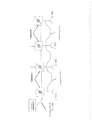
図1は、平面のCPLアンテナ100の例を図示する。この例において、平面のCPLアンテナ100はプリント回路板(PCB)104上に印刷されループエレメント108を含んでいる。それは、2つの端部112および116を提供する開いたベース部を備えた長方形エッジに沿うトレースとしてこの場合形成される。1つの端部112は、電流が供給される場合のアンテナの供給ポイントである。他の端部116は接地である。CPLアンテナ100は、J形のトレース124および蛇行トレース128がある放射素子120をさらに含んでいる。この例において、蛇行トレース128はループエレメント108にJ形のトレース124をつなぐように構成される。放射素子120は本質的に共振回路として機能し、共振がアンテナの開閉頻度で生じるように、直列のインダクタンスおよびキャパシタンスを提供する直列共振回路、およびそれらの値が選ばれる。蛇行トレース128を使用する代わりに、J形のトレース124の形および次元は、ループエレメント108に直接接続し、かつさらにターゲット共振を提供するために調節されてもよい。
FIG. 1 illustrates an example of a
電流が供給されている典型的な従来のループアンテナと同様に、平面のCPLアンテナ100のループエレメント108は磁場(H)を生成する。直列共振回路特性がある放射素子120は、電場(E)ラジエータ(アンテナの本来的な相互性により当然電場レシーバーである)として有効に作動する。ループエレメント108への放射素子120の接続ポイントは、互いに実質的に直角のEとHのフィールドを生成する/受信するための平面のCPLアンテナ100において重要である。この直角の関係は、アンテナによって放射された電磁波が空間を通って有効に拡散することを可能にする効果がある。互いに直角に配置されたEとHのフィールドがない状態で、波は、短距離を越えて有効に拡散しない。この効果を達成するために、放射素子120は、放射素子120によって生成された電場Eが、ループエレメント108によって生産された磁場Hに関して位相が外れた90°または270°である位置に置かれる。具体的には、放射素子120は、供給ポイント112からループエレメント108に沿った、電気的長さが実質的に90°(あるいは270°)の位置に置かれる。あるいは、放射素子120はループエレメント108を通って流れる電流が反映的に最小になる位置でループエレメント108に接続されてもよい。
Similar to a typical conventional loop antenna supplied with current, the loop element 108 of the
電場Eおよび磁場Hの直角に加えて、電場Eと磁場Hが大きさにおいて比較可能であることが望ましい。これらの2つの要因(つまり直角、比較可能な大きさ)は、P=E x H(ボルト/m xアンペア/m=ワット/m2)で定義されたポインティングベクトル(ベクトル電力濃度)に目を向けることにより評価され得る。アンテナを囲む表面から出る総放射出力は、ポインティングベクトルを表面で積分することにより見出される。従って、量E x Hは、放射出力の直接の測定手段であり、したがって、放射効率である。最初に、EとHが互いに直角の場合、ベクトル積が最大を与えることが注目される。次に、2つの産物の全体的な大きさは、より小さなものによって限定されるので、できるだけ接近している2つの量(この場合|H|および|E|)を持っていることは、最適な生成値を与えるだろう。上に説明されたように、平面CPLアンテナにおいて、放射素子120を、供給ポイント112からのループエレメント108に沿った電気的長さが実質的に90°(あるいは270°)の位置に、置くことにより、直角が達成される。更にループエレメント108および放射素子120の形および次元は、比較可能で、強度がそれぞれ高い|H|および|E|を提供するように、それぞれ形成することが可能である。したがって従来のループアンテナとは好対照に、平面CPLアンテナは単に送信と受信モードの両方を提供するだけでなく、放射効率を増加させるように構成することが可能である、
In addition to the right angle of electric field E and magnetic field H, it is desirable that electric field E and magnetic field H be comparable in magnitude. These two factors (ie, right angle, comparable magnitude) look at the pointing vector (vector power concentration) defined by P = E x H (volts / m x amps / m = watts / m 2). Can be evaluated. The total radiated power emanating from the surface surrounding the antenna is found by integrating the pointing vector at the surface. Thus, the quantity E x H is a direct measure of radiant power and is therefore radiative efficiency. First, it is noted that the vector product gives the maximum when E and H are perpendicular to each other. Second, the overall size of the two products is limited by the smaller ones, so having two quantities that are as close as possible (in this case | H | and | E |) is optimal Will give a generated value. As described above, in a planar CPL antenna, the radiating
小型化は、ループエレメントに直列のキャパシタンス及び/又はCPLアンテナの放射素子を導入することによって、達成することが可能である。そのようなアンテナ構造は、容量連結型複合ループアンテナ(C2CPL)と呼ばれ、より大きな効率を備える送信および受信モードの両方と、従来アンテナより小さなサイズとを提供するために開発された。
C2CPLアンテナの構造と実施の例は、2012年11月5日に出願された「容量結合型複合ループアンテナ」と題する米国特許出願No.13/669,389号に述べられている。
LDA+CPLアンテナ
Miniaturization can be achieved by introducing a capacitance in series with the loop element and / or a radiating element of the CPL antenna. Such an antenna structure, referred to as a capacitively coupled complex loop antenna (C2CPL), was developed to provide both transmit and receive modes with greater efficiency and smaller size than conventional antennas.
An example of the structure and implementation of a C2CPL antenna is described in US patent application no. 13 / 669,389.
LDA + CPL antenna
典型的な実施例では、対数検波増幅器(LDA)は、アンテナに直接統合される。前述の参照によって組み込まれた米国特許7,911,235号、または、本出願と同日に出願され、さらに参照によってここに組み込まれた関連すると共に継続中のPCT出願(依頼者整理番号101607.000129、101607.000131および101607.000145)に概略的に記述されたタイプのLDA回路は、次を含む各種機能を、一部は同時に果たすことが可能である:対数検波および増幅、信号再生成、同一入出力周波数での低雑音増幅、、周波数変換、ノイズフィルタリング、混信阻止、およびアナログ/デジタル振幅、位相および周波数復調。これらの機能は、感度および帯域幅を増大させ、電源消費を低下させ、混信阻止と信号対雑音比を改善し、および、デジタルおよびアナログAM、FMおよびPM入力の無線範囲を拡張する。LDA技術の特定のアプリケーションは多数である。 In an exemplary embodiment, a logarithmic detection amplifier (LDA) is integrated directly into the antenna. U.S. Patent No. 7,911,235, incorporated by reference above, or a related and pending PCT application (Requester Docket No. 101607.000129) filed on the same day as this application and further incorporated herein by reference. 101607.000131 and 101607.0000145), LDA circuits of the type schematically described can perform various functions simultaneously, including the following: logarithmic detection and amplification, signal regeneration, identical Low noise amplification at input and output frequencies, frequency conversion, noise filtering, crosstalk rejection, and analog / digital amplitude, phase and frequency demodulation. These features increase sensitivity and bandwidth, reduce power consumption, improve interference rejection and signal-to-noise ratio, and extend the radio range of digital and analog AM, FM and PM inputs. There are many specific applications of LDA technology.
典型的な実施例中のCPLアンテナとLDAとの組み合わせは、例えば、無線LANアプリケーションのための無線通信を大幅に改善することが可能である。前に言及したように、無線通信での重要な制限は、スループットおよび無線範囲を厳しく低減し得る干渉のレベルである。これは恐らく、多くのワイヤレス・ルーターが存在し、それらのどれもがともに(住宅から住宅)同期されない住宅地区で展開した時のWi−Fiのための主な制限のうちの1つである。ルーターはそれぞれ他のものによって悪者アクセス・ポイントと見なされ、これは、ごく近くにいる場合、大きな干渉レベルを生成する。干渉は、各ルーターにデータ比率の後退を強制し、最小のビット誤り率(BER)を維持するために、それをより低いレベルまで低下させる。ますます多くの人々が、無線ルーター、アクセス・ポイント、中継器、コンピューター、タブレット、携帯電話、テレビ、ゲーム機などを所有している。さらに、隣人はそれぞれ自分の家の中に同様の設備を所有し、その結果、他の隣人の近くの無線LANは競合を起こす。これが、チャンネルのオーバーラッピングの干渉取り消しの主な原因である。この競合は、クライアントがそのルーターからより遠くなるにつれ、また、付近のWLANの中の競い合うルーターへ近づくにつれ、帯域幅を低減する。CPLアンテナとLDAとの組合せは、この取り消しを低減するか除去するために、各クライアントおよびそのルーター上で、同期することが可能であり、それによって、無線ルーターとそれらのクライアントの間で、より大きな選択性、範囲および帯域幅を提供する。 The combination of the CPL antenna and LDA in the exemplary embodiment can greatly improve wireless communication for wireless LAN applications, for example. As previously mentioned, an important limitation in wireless communications is the level of interference that can severely reduce throughput and radio range. This is probably one of the main limitations for Wi-Fi when there are many wireless routers and none of them are deployed together in a residential area that is not synchronized (from home to home). Each router is considered a bad access point by others, which generates a large level of interference when in close proximity. Interference forces each router to regress on the data ratio and lower it to a lower level in order to maintain a minimum bit error rate (BER). More and more people own wireless routers, access points, repeaters, computers, tablets, mobile phones, TVs, game consoles, and so on. In addition, each neighbor owns similar equipment in his home, and as a result, wireless LANs near other neighbors create contention. This is the main cause of interference cancellation of channel overlapping. This contention reduces bandwidth as the client gets further from the router and approaches the competing router in the nearby WLAN. The combination of CPL antenna and LDA can be synchronized on each client and its router to reduce or eliminate this cancellation, and thus more between the wireless router and their clients. Provides great selectivity, range and bandwidth.
WLAN、WANおよびWi−Fiは、所要のチャネルと同期した2つのLDAを、低IF変換率を有するCPL(商標)アンテナと組み合わせることによって、および(デジタル入出力の場合)2つのアナログ/デジタル変換器の、周波数デジタル変換器への置換によって、優れた受信感度、干渉取り消しおよび帯域幅を達成する。LDAは、QPSK変調を使用して、デバイスの再生デジタル出力を増強し、これが次に、チャネル間の識別力の向上により、干渉取り消しを低減する。さらに異なるアンテナおよび同調部分の使用によって、同じワイヤレス受信器技術は、WLAN、XMサテライトおよびWi−Fi信号を受信および復調することも可能である。 WLAN, WAN, and Wi-Fi combine two LDAs synchronized with the required channel with a CPL ™ antenna with low IF conversion ratio and (for digital input / output) two analog / digital conversions By replacing the transmitter with a frequency digital converter, excellent reception sensitivity, interference cancellation and bandwidth are achieved. LDA uses QPSK modulation to enhance the playback digital output of the device, which in turn reduces interference cancellation by improving discrimination between channels. By using different antennas and tuning parts, the same wireless receiver technology can also receive and demodulate WLAN, XM satellite and Wi-Fi signals.
典型的な実施例の中で、LDAは、クライアント・ルーターが使用するべき最良チャネルを見つけるため、および、隣接したチャネルまたはオーバーラップするチャネルを強度差および位相微分を使用してフィルタリングするために、フェーズロックループ(PLL)回路を使用してもよい。PLLを備えたLDAは、干渉よりも6dB強く、現存システムよりも3dB強い信号を識別することが可能である。 In an exemplary embodiment, an LDA finds the best channel that a client router should use, and filters adjacent or overlapping channels using intensity differences and phase derivatives. A phase-locked loop (PLL) circuit may be used. An LDA with a PLL can identify signals that are 6 dB stronger than interference and 3 dB stronger than existing systems.
さらに、IF範囲中の周波数変調への入力信号の変換、および対数展開の使用は、ノイズ低減に特に効果的であり、低い信号対雑音比を備えた弱い信号のダイナミックレンジを拡張する。それによって、超音波、MRIおよびCATスキャンなどのような微小信号医療機器、一般的な魚群探知機およびソナー、衝突防止装置および他のアプリケーションと同様に、跳ね飛ばす傾向のレーダーの感度および範囲(および電力消費の減少)を増加させる。 Furthermore, the conversion of the input signal to frequency modulation in the IF range and the use of logarithmic expansion is particularly effective for noise reduction, extending the dynamic range of weak signals with low signal-to-noise ratios. Thereby, the sensitivity and range of radars that tend to jump (and small signal medical devices such as ultrasound, MRI and CAT scans, general fish finder and sonar, anti-collision devices and other applications) (and Increase power consumption).
さらに、LDAがより弱い信号からのランダムノイズをフィルタリングする能力はそれらに、いくつかのまたはより多くのdBs対最良低雑音増幅器(LNA)のような、非常に弱い信号を再生成するための手段を与える。LNA未満の全般的な消費に加えて、全面的により良好なリンクバジェット(link budget)である追加の受信感度を考慮する数dBによって、通信の両側のRF送信出力が低減されるかもしれない。携帯電話の出力電力をさらに低減するため、および、それによって、バッテリー寿命およびその範囲を3時間まで延長するために、LDA技術は、電話機のICチップ内へ直接組み込むことが可能である。 Furthermore, the ability of LDA to filter random noise from weaker signals allows them to regenerate very weak signals, such as some or more dBs versus best low noise amplifiers (LNA). give. In addition to the overall consumption below the LNA, the RF transmit power on both sides of the communication may be reduced by a few dB that takes into account the additional receive sensitivity, which is a better link budget overall. In order to further reduce the output power of mobile phones and thereby extend battery life and its range to 3 hours, LDA technology can be incorporated directly into the IC chip of the phone.
LDAはさらに、より高いデータ容量用の、複数のアクティブアンテナ、プラス802.11ac/MIMO、および直角周波数分割多重化(OFDM)のための高性能デジタル無線受信機の解決手段の核心であり得る。そのような構成では、CPLアンテナはそれぞれ、高性能のLDAベースに基づいたレシーバーであってもよい。LDAがアンテナに接続される場合、それは、各アンテナ間の分離を支援する。 LDA can also be at the heart of high performance digital radio receiver solutions for multiple active antennas, plus 802.11ac / MIMO, and orthogonal frequency division multiplexing (OFDM) for higher data capacity. In such a configuration, each CPL antenna may be a receiver based on a high performance LDA base. When the LDA is connected to an antenna, it assists the separation between each antenna.
さらにより詳細に下に記述されるように、LDAも電子的にステアリングアンテナ上で実装することが可能である。さらに、CPLアンテナは、アプリケーションに適切なように、ここに記述された実施例中の従来の広帯域アンテナと取り替えてもよい。 As described in more detail below, LDA can also be implemented electronically on a steering antenna. In addition, the CPL antenna may be replaced with the conventional broadband antenna in the embodiments described herein as appropriate for the application.
図2は、代替または隣接チャネルにおいて、いくつかのOFDM信号が共存しまたは干渉し得るか、あるいは同一チャネル干渉により悪化しているWi−Fi 802.11の2.4−2.5GHzの帯域の出力レベル対周波数特性を示す。LDAは、これらの状況の全部において、その周波数帯幅が1つのチャネルの幅に限定されるとき、それを選択し、その周波数帯幅の外側の信号を抑えることを支援することが可能であると認められるであろう。LDAは、レシーバーのマスタークロックおよび反対側の所望の送信器で位相が固定される(および悪者APとは位相が外れる)ので、PLLを備えたチャネルへロックされてもよく、さらに同一チャネル干渉に対し支援してもよい。
典型的なLDA
FIG. 2 illustrates the Wi-Fi 802.11 2.4-2.5 GHz band where several OFDM signals may coexist or interfere in an alternate or adjacent channel or are degraded by co-channel interference. The output level vs. frequency characteristics are shown. In all of these situations, the LDA can help to select when its frequency bandwidth is limited to the width of one channel and suppress signals outside that frequency bandwidth. It will be recognized. The LDA is locked in phase with the receiver master clock and the desired transmitter on the opposite side (and out of phase with the rogue AP), so it may be locked to a channel with a PLL, and further to co-channel interference. Support may be provided.
Typical LDA
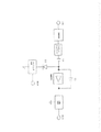
前述の米国の特許7,911,235号に述べられていたLDAに加え、本発明は、構成に依存するLDAの種類のうちのどれでも実装してよい。例えば、図3は、対数検出器100の実施例を図示するブロック・ダイヤグラムである。この実施例では、入力端子からの入力信号は、INPUTと称され、増幅回路104によって受信されるであろう。増幅回路104は入力信号を増幅するように構成され、演算増幅器、バイポーラ接合トランジスタ(BJT)、電界効果トランジスタ(FET)または他の離散トランジスタ、真空管、RF増幅器などのような、任意の適切な増幅要素を含んでもよい。発振は、電気雑音及び/又は所望の信号に反応して、増幅回路100において開始されてもよい。発振は、入力信号の強度に応じて周期的に停止してもよい。帰還回路に構成されることができる共振回路108は、動作頻度を制御するために、増幅回路104に並列に接続されてもよい。図3の実施例において、共振回路108は一連のLC回路を含んでもよく、その場合、LとCの値が、対数検出器100の動作頻度に相当する共振周波数を有するように選択されてもよい。発振は、LとC値によって測定された周波数の増幅回路104において設定されてもよい。したがって、LC共振の外部のノイズは、LC回路の動作に与える影響が最小である。LC共振の帯域幅内の入力信号は、発振を、ランダムノイズのみよりも、急速に開始させてもよい。標準感度あるいは回路の要因Qは、共振回路108内で使用される構成要素によって大部分が測定されてもよい。高Q回路は、例えば共振回路108内の水晶共振子の使用によって、達成されるかもしれない。
In addition to the LDA described in the aforementioned US Pat. No. 7,911,235, the present invention may be implemented with any type of LDA that depends on the configuration. For example, FIG. 3 is a block diagram illustrating an embodiment of the
サンプリング回路112は増幅回路104に接続されてもよい。サンプリング回路112は、するように形成されてもよい。電圧補給線を増幅回路104へ流れる電流を有効にサンプリングするために、;一旦、予め測定されたしきい値が到達すると、サンプリング回路112は、発振を止めるために動作してもよい。すなわち、サンプリング回路112は、しきい値が到達する各時点に、周期的に発振を中断するために使用されてもよい。
周波数対電圧変換器116はサンプリング回路112に接続されてもよい。周波数対電圧変換器116への入力は、本明細書でさらに記述したように、繰り返し周波数Frepとして表示される、一連の電圧スパイクを含んでもよく、その周波数は、入力信号の出力の対数として、実質的に変化する。周波数対電圧変換器116からの出力は、入力スパイクの周波数に比例する直流電圧でもよい。
The
The frequency to
入力信号が調整される場合、周波数‐電圧変換器116の出力は、直流電圧成分および交流電圧成分を含んでもよい。AC成分は入力変調に対応してもよく、および、有効的に、ベースバンドにおける復調された入力信号のコピーでもよい。
If the input signal is adjusted, the output of the frequency-to-
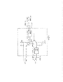
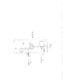
上に説明された対数検波器の実施形態は、様々な電子工学応用のために実施される様々な方法で適応させてもよい。対数検出器増幅器(LDA)システムには一定の基礎的な特性が供給されてもよく、ターゲット・アプリケーションでの適切な性能強化のために修正されてもよい。図4は、LDAシステムの実施形態200を示すブロック・ダイヤグラムである。LDAシステム200は分離回路204、マッチングネットワーク208、LDA核心212、ブースタ回路216および周波数‐電圧変換器220を含んでいてもよい。OUTPUT 1として呼ばれる、出力はこの例における周波数‐電圧変換器220に連結されてもよい。ブースタ回路216および/または周波数‐電圧変換器220は、任意の要素であってもよい;それらのうちの1つまたは両方はターゲットアプリケーションによって省略されてもよい。LDAシステム200がブースタ回路216および周波数‐電圧変換器220を含まない場合、図4中のOUTPUT 2によってあらわされるように、出力ポートはLDA核心212から離れて直接置かれてもよい。LDA核心212は増幅回路224、共振回路228およびサンプリング回路232を含んでいてもよく、増幅回路104、共振回路108、および図3の対数検波器100のサンプリング回路112と同様に作動し、機能するよう構成してもよい。
The logarithmic detector embodiments described above may be adapted in various ways implemented for various electronics applications. A logarithmic detector amplifier (LDA) system may be provided with certain basic characteristics and may be modified for proper performance enhancement in the target application. FIG. 4 is a block diagram illustrating an
分離回路204は電力漏れ、LDA核心212による反射信号、およびRxチェーンを保護し、再生を最適化するために周囲の回路、特にTxチェーン、による他の干渉効果をフィルタするために使用される。特に、入力された信号と位相関連性が不明であるとして分離回路204に入力されるLDA核心からの反射し戻る信号は再生強化工程が同時の場合、信号再生に有害な効果があるかもしれない。反射され、入力信号とまざっている位相信号から、再生工程は所望に達成することができず乏しい性能が生じうる。
漏れた電力もまた、アンテナのような受信入力への道を見つけるかもしれず、不要発射またはEMIとして放射される。分離回路204は、そのような分離を目的としてサーキュレータを含んでいてもよい。Rxチェーン中のサーキュレータは、Rx信号をアースへ通し、かつ不要な漏れおよび反射をショートさせるように構成されてもよい。典型的なサーキュレータは、非線形性を修正するためにフェライトのような強磁性の要素を含んでいる。しかしながら、強磁性の要素は典型的にかさばっていて高価である。サーキュレータの代わりに、分離回路204は低雑音増幅器(LNA)あるいはどんな受動または、能動素子も持つように構成されてもよく、それは高められた利得(能動回路用)、向上した分離、信号対雑音比および帯域幅を供給してもよい。マッチングネットワーク208はインピーダンス・マッチングおよび/または位相補正目的に用いられてもよい。図3で説明されたものと同様の機構に基づいて、LDA核心212は一連の電圧スパイク、Frep、入力信号の電力の対数として本質的に変わる周波数を出力してもよい。信号のFrepはOUTPUT 2から出力されてもよく、あるいはブースタ回路216および/または、さらにOUTPUT 1から処理され出力するため周波数対電圧回路220に送信されてもよい。ブースタ回路216は、例えば約100mVから数Vまで信号Frepを増幅するために、1以上のトランジスタまたは他の適切な増幅構成要素を含んでいてもよい。ブースタ回路は、より純粋でかつより鋭いスパイクを得るために増幅されたFrepをデジタル化するために、シュミットトリガ回路あるいはデジタル・インバーターのような任意の単純なデジタル回路をさらに含んでもよい。ブースタ回路216による出力信号は、信号がOUTPUT 1から出力されるために可聴周波数のような、DCおよびAC電圧に変換されるよう、周波数‐電圧変換器220に送られてもよい。
Leaked power may also find a way to receive inputs such as antennas and radiate as unwanted emissions or EMI. The
前に言及されるように、LDAシステム200はターゲットアプリケーションに対してふさわしい性能強化と同様に、図3で示されるような対数検波器の一定の基礎的な特性を含んでいてもよい。例えば、作動の周波数は、共振回路のLおよびC値の選択により決定されてもよい。;そのため、LDA核心増幅回路と共に、高いバンド外拒絶、高いスカート比率および高い信号対雑音比は、種々に修正されるようなLDAシステム200を用いることにより達成されてもよい。すなわち、LDAシステム200は、高度な、周波数選別応用のために実施されてもよい。更に、サンプリング回路は、しきい値に到達し、しきい値が到達するごとに、周期的に発振を中断し、自己ケンチングおよび時間依存のサンプリング機能を供給してするために用いられてもよい。したがって、発振の再生特性は、増幅回路の低い即時の再生利得及び、発振をとめ再開することにより高められてもよく、高いRx感度を高めてもよい。増幅回路の低い即時の再生の利得は、実施形態1乃至 5の範囲中にあってもよい。しかしながら、再生の全サイクルにわたるLDA利得は本質的により高くてもよい。典型的に、例えば−10dBから+50dBの範囲で最低値から最高値であってもよい。典型的なLNAと比較して、信号対雑音比は高められてもよく、出力受信信号インジケータ(RSSI)レベルはより高くなってもよい。これは、続く受信段階、あるいは通信装置にとって都合がよく、通信装置においてLDAは更なる増幅をあまりまたは、まったく要求されないのでシステム200が用いられる。LDAのRx感度は、キャパシタ、誘導子、SAWフィルタ、BAWフィルタ、セラミック共振器、機械工共振器などのような共振回路の中で高いQ構成要素を用いることにより達成されるかもしれないLDA核心の周波数帯域幅を弱めることにより、増加されてもよい。誘導子とキャパシタ用の高Q値は実施形態中で25乃至200の範囲中にあってもよい。SAWフィルタ、BAWフィルタ、セラミックフィルターおよび機械工フィルタ用の高Q値は、特に500乃至20,000の範囲中にあってもよい。
As previously mentioned, the
実施形態は弱い乃至強い受信信号を再生することができてもよく、また通常対数増幅器に関係している周波数の変換なしに、最小のノイズの追加でそれを選択的に増幅できてもよい。 Embodiments may be able to reproduce a weak to strong received signal and may be able to selectively amplify it with minimal noise addition, without the frequency conversion normally associated with logarithmic amplifiers.
図5Aは、LDAシステムの他の実施形態300を示すブロック・ダイヤグラムである。LDAシステム300は分離回路304、マッチングネットワーク308およびLDA核心312を含んでいてもよい。LDA核心312は増幅回路324、共振回路328およびサンプリング回路332を含んでいてもよく、それは同様に作動し機能するように増幅回路104、共振回路108、および図3の対数検出器100のサンプリング回路112で構成してもよい。OUTPUT Aは図4のOUTPUT 2と同じであり、LDA核心312は一連の電圧スパイク、Frepを出力してもよい。あるいは、出力されずに、ここでFrepは中断してもよい。LDAシステムの例300では、共振回路328はOUTPUT Bを通してRF信号を出力するように構成されてもよい。図3および4のOUTPUTまたはOUTPUT2がINPUT周波数に対して異なる周波数にある場合がLDAに反して、OUTPUT BはINPUT周波数と同じ周波数を実質上有する。信号はINPUT信号のコピーであり、併せてサンプリングされて、及び図15のようにみえてもよい。これは、LDAのこの構成を図6の中の300中に示されたようなLNA交換あるいはLNA補足適用に対して特に適するようにする。
FIG. 5A is a block diagram illustrating another
集積AM/ASK/OOK復調回路を備えたLDAのさらなる実施形態は、図5B中で示される。図5Bは、本質的に図5Aと同じであるが、マッチングネットワークおよび他の出力を生じる、次の低域フィルタの追加を備えている。代替出力中の信号は本質的にRF周波数構成要素が低域フィルタで除去された後どんなAM/ASK/OOKも含む入力信号の再生された時間サンプリングコピー(time sampled copy)を生み出す。エネルギー伝達を分離し最大限にするために、マッチング回路は低域フィルタの前に追加されてもよい。 A further embodiment of an LDA with integrated AM / ASK / OOK demodulation circuit is shown in FIG. 5B. FIG. 5B is essentially the same as FIG. 5A, but with the addition of the following low-pass filter that yields a matching network and other outputs. The signal in the alternate output essentially produces a regenerated time sampled copy of the input signal that contains any AM / ASK / OOK after the RF frequency components have been removed by the low pass filter. A matching circuit may be added before the low pass filter to isolate and maximize energy transfer.
出力信号のタッピングは、増幅器の出力のような伝導モード、または相互につながれたインダクタンスとの電磁結合のような無線モード中に行われてもよい。時間サンプリングにより、周波数スペクトルは繰り返すように見えてもよい。ある場合には、ケンチング周波数パルスが、あたかもケンチング周波数がなく、出力上で変調された信号が同時に連続的に表れるように、システムが作用することがほとんどないかもしれない。しかしながら、代替出力ノードでタッピングすることは、この問題を和らげて、より高い電力出力信号F_rep(t)を供給してもよい。 The tapping of the output signal may be done in a conduction mode, such as the output of the amplifier, or in a wireless mode, such as electromagnetic coupling with the coupled inductances. With time sampling, the frequency spectrum may appear to repeat. In some cases, the system may have little effect so that the quenching frequency pulses have no quenching frequency and the modulated signal on the output appears continuously at the same time. However, tapping at an alternative output node may alleviate this problem and provide a higher power output signal F_rep (t).
低域フィルタの前の交互の出力中の周波数スペクトルは、(もしあれば)変調されたRF信号、(もしあれば)変調を備えた中間周波数IFの中の反復率f_rep(t)周波数及び、(もしあれば)0ヘルツのベースバンド中に変調された信号を含んでいてもよい。この点で、2つのケースが可能となる:
1. 低域フィルタ、RF信号およびIF周波数(f_rep)及び再生/増幅されたベースバンド信号を回復。
ベースバンド信号は復調されたAM出力が起こる。
任意に、アンチエイリアスフィルターのあとデジタル信号v(k)を形成するADCは可能である。
2. 低域フィルタ(あるいはバンドパスフィルタ)RF信号およびベースバンド(BB)周波数、及び再生/増幅されたf_rep(t)信号の回復。
AM信号を復調するまたはベースバンドを回復する周波数‐電圧変換器、f/vコンバーターおよび改変した増幅器を備えたアナログ方式工程f_rep(t)。
任意に、アンチエイリアスフィルターのあとデジタル信号v(k)を形成するADCで対応することは可能である。
b.デジタルに、デジタル波整形、瞬時周波数メーター(あるいはデジタル1/x機能のあとのペリオド計)およびデジタル復調出力信号を得るためにスケーリングする工程f_rep(t)。
The frequency spectrum in the alternating output before the low pass filter is the modulated RF signal (if any), the repetition rate f_rep (t) frequency in the intermediate frequency IF with modulation (if any), and It may contain a modulated signal in the baseband of 0 Hz (if any). In this respect, two cases are possible:
1. Recover low pass filter, RF signal and IF frequency (f_rep) and regenerated / amplified baseband signal.
The baseband signal has a demodulated AM output.
Optionally, an ADC that forms a digital signal v (k) after an anti-aliasing filter is possible.
2. Recovery of the low pass filter (or bandpass filter) RF signal and baseband (BB) frequency and the regenerated / amplified f_rep (t) signal.
Analogue process f_rep (t) with frequency-voltage converter, f / v converter and modified amplifier to demodulate AM signal or recover baseband.
Optionally, an ADC that forms a digital signal v (k) after an anti-aliasing filter can accommodate this.
b. Digitally scaling to obtain digital wave shaping, instantaneous frequency meter (or period meter after digital 1 / x function) and digital demodulated output signal f_rep (t).
さらなる実施形態は図5Bの中に示される。図5Bは、LDAを集積AM/ASK/OOK復調回路出力および交互の出力で示す。図5Bの中で、また、上記の節中にリストされるように、f_rep(t)信号は、マッチングネットワーク2の後、R1、C3の上で出力のようなノードでタップすることができる。あるいは、出力は増幅器、あるいは並列共振回路からの分離したキャパシタ中央ノードの上誘導され、あるいは代わりに増幅器の入力側上での出力から誘導される。これらの選択肢のいずれかは、出力を得るためにマッチングネットワークと低域フィルタに続く。
A further embodiment is shown in FIG. 5B. FIG. 5B shows the LDA with integrated AM / ASK / OOK demodulator output and alternating outputs. In FIG. 5B and as listed in the above section, the f_rep (t) signal can be tapped at a node such as an output on R1, C3 after the
図5Cは、AM及びPMの復調能力を備えたLDAの回路図の実施形態を描く。AM復調能力を備えたLDAの典型的な実想は、図5Cで示される。並列及び直列の共振器回路L1、C3は、増幅器T1、この場合はNPNトランジスタのコレクタ上で発見される。180度の位相を供給するトランジスタT1は、コレクタとエミッタの間でシフトする。C1は帰還発振器キャパシタである。VG1は、キャパシタ(図示せず、しかし図5〜8中に示されるキャパシタC2のようなもの)を介してつながれた、入力源信号である。バイアスはVS2、R3およびC6ある。
D2はRC回路R4、C11に対する二極管カップリングである。出力はVM1である。任意のC7はケンチング工程を向上させるために示される。
FIG. 5C depicts an embodiment of a schematic diagram of an LDA with AM and PM demodulation capabilities. A typical idea of an LDA with AM demodulation capability is shown in FIG. 5C. Parallel and series resonator circuits L1, C3 are found on the collector of the amplifier T1, in this case the NPN transistor. Transistor T1 supplying 180 degrees phase shifts between the collector and emitter. C1 is a feedback oscillator capacitor. VG1 is an input source signal connected via a capacitor (not shown, but like capacitor C2 shown in FIGS. 5-8). The bias is VS2, R3 and C6.
D2 is a bipolar coupling to the RC circuits R4 and C11. The output is VM1. Optional C7 is indicated to improve the kenching process.
FIG 5Aに戻り、分離回路304は、出力漏洩、周囲の回路、特にTxチェーンからの反射信号、および他の干渉効果をフィルタリングするため、Rxチェーンを保護するため、および、先に説明したように、再生効率の低減またはEMIとしての放射出力漏洩を避けるために、使用されてもよい。分離回路304は、分離目的のためのサーキュレータを含んでもよい。Rxチェーン中のそのようなサーキュレータは、Rx信号、および、望まれない漏洩の短絡、および接地への反映を通過させるように構成されてもよい。典型的なサーキュレータは、フェライトのような、適正な非線形性の強磁性要素含んでいてもよい。しかしながら、強磁性のエレメントは全般的にかさばっていて高価である。代替物は、サイズを劇的に縮小し得るナノチューブ・メタ材料サーキュレータを使用することである。サーキュレータの代わりに、分離回路304が、増強された利得(能動回路用)、分離、信号対雑音比および帯域幅を提供し得るLNA、または任意の受動的または能動的素子を有するように構成されてもよい。 Returning to FIG. 5A, the separation circuit 304 is used to filter output leakage, surrounding circuitry, particularly reflected signals from the Tx chain, and other interference effects, to protect the Rx chain, and as described above. It may be used to reduce regeneration efficiency or avoid radiated output leakage as EMI. Separation circuit 304 may include a circulator for separation purposes. Such circulators in the Rx chain may be configured to pass the Rx signal and unwanted leakage shorts and reflections to ground. A typical circulator may include a properly nonlinear ferromagnetic element, such as ferrite. However, ferromagnetic elements are generally bulky and expensive. An alternative is to use a nanotube metamaterial circulator that can be dramatically reduced in size. Instead of a circulator, the isolation circuit 304 is configured to have an LNA that can provide enhanced gain (for active circuits), isolation, signal-to-noise ratio and bandwidth, or any passive or active element. May be.
マッチングネットワーク308はインピーダンス・マッチング及び/又は位相補正目的に使用されてもよい。図3に関して説明されたものと同様の機構に基づき、LDAコア312は一連の電圧スパイク、Frepを出力してもよい。Frepは出力 Aから出力されてもよく、または単に、出力されずに開いたままにしてもよい。
OUTPUTBを通してRF信号を出力するように共振回路328を形成することによって、図5で示されるようなLDAシステムは、様々なRFアプリケーションのために実施され、一方で従来のRF通信装置と比較して高められた業績水準を提供してもよい。図6は、RF信号の送受信のための従来の通信装置の実施形態を示す。単一のアンテナ404はこの例の中で送信(Tx)および受信(Rx)モードの両方に対して用いられてもよい。Tx/Rxスイッチ408は、時間間隔中にモードに依存するTxチェーンあるいはRxチェーンのいずれかを選択するためにアンテナ404につなげられてもよい。Rxチェーンは、通常はRxフィルタ412およびLNA416が有していてもよい。付Rxフィルタは、LNA416、の前か後ろのいずれか、あるいはフィルタレベルおよび周波数範囲の両方に依存して追加されてもよい。LNAは典型的にRx信号を増幅しその一方で、感度を増加するためにノイズと歪みをほとんど加えないため用いられてもよい。Rx信号は増幅され、最終的にLNA416からトランシーバ420に出力され、モデムのようなベースバンド処理装置424に到達する。Txチェーンは、電力増幅器(PA)428およびTxフィルタ432を有していてもよい。付加的なTxフィルタは、PA428の前か後ろ化のいずれか、あるいはフィルタレベルおよび周波数範囲の両方に依存して加えられてもよい。Tx信号は、トランシーバ420から出力されるTx信号は、PA428に送られてもよく、Tx信号は増幅されTxフィルタ432に出力され、この実施形態に示されるようにアンテナ404に送られてもよい。トランシーバ420は、RF信号を処理するために様々な回路を含んでいてもよい。これらの回路は、図6中に表わされ、Rxチェーン用Rx信号処理回路436が、Txチェーン用Tx信号処理回路440などがある。Rx信号処理回路436は、周波数をダウン変換するためのダウンコンバーター、変調された信号を復調するための復調器、ベースバンド処理装置424へ入力されるデジタル信号を生成するアナログ・デジタル変換器、および遠隔送信機から、レシーバーとともに入力シンボル・データ・ストリームを同調させるための同期機能を含んでいてもよい。
By forming the
従来のRF通信装置は図6で示され、LNA416はRx信号に増幅され、一方で、典型的にノイズと歪みをほとんど加えない。前に説明されるように、LDAシステムは不要なノイズを最小化する一方で増幅された信号を供給することができる。したがって、高められた性能レベルを備える新しいRF通信装置のタイプは、図6の中の点で描いた四角によって示されるように、RF出力、OUTPUT Bをトランシーバ420につなぐことで、LNA 416をLDAシステム300に置換して供給してもよい。あるいは、LDAシステムはLNAを補足するために受信感度ブースタとして最初のあるいは後の増幅段階として追加されてもよい。自由に、LDAは、受信チェーンにおける高い利得のLNAの後に追加され、さらに、線形回路で可能でないシステム雑音係数を弱めることができる。これは、繰返し信号が多くのCWサイクルにわたり存在する場合に、信号対雑音比を増加させることを可能にするLDAの再生要因による。Rxフィルタ412および他の構成要素もまたLDAシステム中に含まれていてもよい。通信装置がWiFiシステムである場合に、約2.4GHzにおけるRF信号はLDAシステム300によって増幅され、ダウンコンバーターを含むトランシーバ420へ出力されてもよい。典型的なダウンコンバーターは、間周波数を中心とする中間周波数信号を超長波を中心とするベースバンド信号に変換する。したがって、LDAシステム300のRF出力、OUTPUTBから約2.4GHzでRF Rx信号をえることによって、ダウンコンバーターを含む既存のトランシーバー・テクノロジーは、ベースバンドプロセッサ424に送信されるWi−Fi 802.11b 乃至802.11acのために、ダウンコンバート信号、約20MHzから160MHzを獲得するような修正なしで用いられてもよい。
A conventional RF communication device is shown in FIG. 6, where the LNA 416 is amplified into an Rx signal, while typically adding little noise and distortion. As explained previously, the LDA system can provide an amplified signal while minimizing unwanted noise. Thus, a new RF communication device type with an increased level of performance connects the LNA 416 to the LDA by connecting the RF output, OUTPUT B, to the
他の応用は、変調された信号帯域幅が低い数KHzであってもよい168MHz、433MHzあるいは868MHzで使用を目的としてサブー1GHz狭帯域トランシーバに関するものであってもよい。 Other applications may relate to sub-1 GHz narrowband transceivers intended for use at 168 MHz, 433 MHz or 868 MHz, where the modulated signal bandwidth may be as low as several KHz.
さらに他の応用は、衛星通信、例えば1.5GHzのGPSを考慮し、受信した無線信号が非常に低い電力レベル、典型的に受信逆拡散の前のノイズ・フロアまでであってもよい。 LDAは、そのような非常に低い受信レベル、搬送波に関連のある低データ速度および相対的な低データ速度アプリケーションのための受信ブースタとしてのすぐれた候補であってもよい。 Still other applications may consider satellite communications, eg, 1.5 GHz GPS, where received radio signals may be at very low power levels, typically up to the noise floor prior to receive despreading. The LDA may be a good candidate as a reception booster for such very low reception levels, low data rates associated with carriers and relative low data rate applications.
さらに他の応用は、非常に速いトランジスタを備えた単純な電子位相が必要な場合、60GHz帯のような非常に短い周波数に関するものであってもよい。60GHzのCMOSプロセスは、非常に敏感度の良い受信器を供給するためにそのような受信ブースタあるいはLNA交換を設計するために用いられてもよい。 Yet another application may be for very short frequencies such as the 60 GHz band if a simple electronic phase with very fast transistors is required. A 60 GHz CMOS process may be used to design such a reception booster or LNA exchange to provide a very sensitive receiver.
さらに他の応用は、無線から、あるいはケーブル、電源線、電話線、光ファイバーなどを通して送信された様々な変調された通信信号に関してよく、ここで搬送波および/または変調された信号の電力が、高い感度、およびノイズの増加により増幅され、さらに、受信器ユニットによって処理されることが望まれる。 Still other applications may relate to various modulated communication signals transmitted wirelessly or through cables, power lines, telephone lines, optical fibers, etc., where the power of the carrier wave and / or the modulated signal is highly sensitive. , And due to the increase in noise, it is desired to be further processed by the receiver unit.
図5の中のLDAシステムは、CW RF信号(変調されず)あるいは変調信号を備えたRF搬送波信号のいずれかを増幅してもよい。変調信号は、アナログ振幅、周波数変調あるいは位相変調、(それぞれ短縮されてAM、FM、PM)のデジタル変調の場合であってもよくあるいは変調の異なるタイプとして当業者が既知の略語であるASK、OOK、直角位相m−AM、FSK、MSK、GFSK、GMSK、4−FSK、4GMSK、m−FSK、PSK、QPSK、m−PSK、m−QAMのいずれかであってもよい。変調の異なるタイプとして当業者が既知の略語であるFH−SS、DS−SS、OFDM、BPSKを備えたMIMO NxN、QPSK、m−QAMおよびOFDMのような、より複雑な変調は使用されてもよい。典型的な意味では、図5で示さるように、LDAシステム300は、高い受信感度により再生及び増幅し、低い雑音は再生度数帯域幅内のINPUTからの入力を表し、及びOUTPUTB上での周波数変換(つまり同じ周波数、同じスペクトルによる)信号を出力する。これは搬送波と変調を含んでいる。
The LDA system in FIG. 5 may amplify either a CW RF signal (unmodulated) or an RF carrier signal with a modulated signal. The modulation signal may be a digital modulation of analog amplitude, frequency modulation or phase modulation (AM, FM, PM respectively shortened) or ASK, which is an abbreviation known to those skilled in the art as a different type of modulation. Any of OOK, quadrature phase m-AM, FSK, MSK, GFSK, GMSK, 4-FSK, 4GMSK, m-FSK, PSK, QPSK, m-PSK, and m-QAM may be used. More complex modulations may be used, such as MIMO NxN, QPSK, m-QAM and OFDM with FH-SS, DS-SS, OFDM, BPSK, abbreviations known to those skilled in the art as different types of modulation. Good. In a typical sense, as shown in FIG. 5, the
前に言及されるように、LDAシステム300は、LNA416を交換するよりむしろ、ブロック412と416の間の受信パス内の相補的な方法中でLDAシステム300をくわえることにより受信ブースタとして図6の通信装置を実装してもよい。この構成では、受信感度は、LDA高い受信感度、低雑音指数および増幅によって増加させてもよい。
As previously mentioned, rather than replacing LNA 416,
他の実施形態では、フィルタ412はLDAシステムが増加したスカート比率をパルス発振器および増幅器により選択性周波数回路であるので、取り除かれてもよい。これはフィルタ412の条件を緩めて、それを交換し、帯域外の除去性能をこえてもよい。 In other embodiments, the filter 412 may be eliminated because the LDA system is a selective frequency circuit with a pulsed oscillator and amplifier with increased skirt ratio. This may relax the condition of the filter 412 and replace it to exceed the out-of-band rejection performance.
図7は、LDAシステム300の回路構成の実施形態を示す。分離回路は入力ポートに連結され、Rxチェーンを保護するためかつ再生効率電力の漏出、反射信号、及び周囲の回路による他の干渉効果を除外するために用いられてもよい、および再生効率あるいはEMI放射電力の減少を回避するために用いられてもよい。分離回路は、分離を目的としてサーキュレータを含んでいてもよい。典型的にかさばる高価な強磁性の要素を含むサーキュレータの代わりに、LNA、あるいは高められた利得(能動回路用)、分離、信号対雑音比および帯域幅を供給しうる任意の受動的または能動的装置も備えるように構成されてもよい。マッチングネットワークはインピーダンス・マッチングおよび/または位相補正目的ように用いられてもよい。マッチングネットワークは、この実施形態中のキャパシタC2によって、増幅回路の入力セクションに決定的に連結されてもよい。十分な入力エネルギーがLDA中に導入されないので、過少連結のカップリングは再生工程に悪影響をうけるかもしれない。システムが過剰連結された反対の場合、再生はあまりにも多くの入力エネルギーがLDAに転送されるので、影響されるかもしれない。増幅回路は入力信号を増幅するように構成されてもよく、演算増幅器、BJT、FET、RF増幅器あるいは他の離散的なトランジスタのような適切な増幅要素もまた含んでいてもよい。
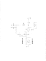
FIG. 7 shows an embodiment of the circuit configuration of the
図7のLDAシステムは、増幅回路の出力側で増幅回路と直列でつながれた共振回路、および増幅回路と並列につながれたキャパシタC1を含んでいてもよい。あるいは、共振回路は増幅回路の入力側で増幅回路と直列で繋げられてもよい。動作周波数は、共振回路のL値およびC値を選ぶことにより設定されてもよい。発振はそのように決定された周波数において増幅回路中で設定されてもよい。この実施形態において、サンプリング回路はダイオードD1を介して増幅回路に連結されてもよい。サンプリング回路は増幅回路までの電圧供給管路中で流れる電流を効果的にサンプリングするように構成されてもよく;前もって定義した閾値に到達した時点で、サンプリング回路は発振を止めるために作用してもよい。すなわち、閾値が到達するごとに、周期的にサンプリング回路の発振を止めるために使用されてもよい。サンプリング回路からの出力はこのように一連の電圧スパイク、Frepであってもよい。FrepはOUTPUT Aから出力されるか、あるいは単に、出力されずに終了してもよい。当業者は、OUTPUT AがFM復調のため異なる周波数を、内外に供給することを認識できる。FM変調に関して、共振回路は少なくとも並列および直列共振回路を必要とする。 The LDA system of FIG. 7 may include a resonant circuit connected in series with the amplifier circuit on the output side of the amplifier circuit, and a capacitor C1 connected in parallel with the amplifier circuit. Alternatively, the resonant circuit may be connected in series with the amplifier circuit on the input side of the amplifier circuit. The operating frequency may be set by selecting the L value and C value of the resonant circuit. Oscillation may be set in the amplifier circuit at the frequency so determined. In this embodiment, the sampling circuit may be coupled to the amplifier circuit via a diode D1. The sampling circuit may be configured to effectively sample the current flowing in the voltage supply line to the amplifier circuit; when the predefined threshold is reached, the sampling circuit acts to stop oscillation. Also good. That is, it may be used to periodically stop the oscillation of the sampling circuit every time the threshold is reached. The output from the sampling circuit may thus be a series of voltage spikes, Frep. Frep may be output from OUTPUT A, or simply terminated without being output. One skilled in the art can recognize that OUTPUT A supplies different frequencies in and out for FM demodulation. For FM modulation, the resonant circuit requires at least a parallel and series resonant circuit.
LDAシステムの特性に影響を及ぼすことが無いRF周波数おける信号出力において、図5あるいは図7の中のLDAシステムの共振回路は、図4、図8で示されるLDAシステム200の共振回路228、LDA特性に影響されない出力RF信号の共振回路の実施形態と異なった構成であってもよい。この共振回路は2つの主要部分:直列共振回路部分および並列共振回路部分を含んでいてもよい。この図では、VCCはDC電圧供給を表わし、共振回路の入力ポートは増幅回路に連結されるように構成されてもよく、出力ポートはRF信号の出力のためにOUTPUTBに連結されてもよい。当業者は、AM、FMおよびPMのようなアナログあるいはデジタル変調のいずれかのタイプに対してOUTPUT Bが同じ周波数を内外に提供することを認識するにちがいない。OUTPUTAを用いた直接のFM復調に関して、共振回路は少なくとも並列および直列共振回路を必要としてもよい。しかしながら、LDA周波数応答の正規曲線の右の傾斜あるいは左の傾斜のほぼ真中に位置するようなに位置するINPUT信号がLDA中央周波数の僅か左に位置するように勾配検出により直列共振回路のない狭帯域FMを復調することは可能である。 広帯域のFM信号は、LDAのQファクターが適応するように減少する場合に右か左の勾配上に入力信号の広帯域の偏差を提供するのと同様に直接判別することができる。OUTPUT Aを通したAMおよびPM復調に関しては、直列の共振は必要ではない。直列共振部分は、キャパシタCSおよび誘導子LSを含んでいてもよく直列共振を供給する。並列共振回路部分は、分離したキャパシタCP1およびCP2と並列の誘導子LP、およびCP1とCP2のコモンノードに連結された第3のキャパシタCCを含んでいてもよい。非常に互いを連結し、かつ出力インピーダンスのために最適化するようにCP1、CP2およびCCの値を決定することによって、RF信号は最適にタップ(Tapped Out)する。更に、並列共振回路部分中の誘導子およびキャパシタのうちのいくつかは高められた感度を備えた小さな帯域幅を持つように高いQ誘導子および高いQキャパシタであるように構成されてもよい。
In the signal output at the RF frequency that does not affect the characteristics of the LDA system, the resonant circuit of the LDA system in FIG. 5 or FIG. 7 is the resonant circuit 228, LDA of the
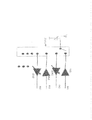
図9は、RF_OUTからRF_INまですすむより黒い線902によって示されたリバースRF出力RF_INからアンテナを駆動するために逆方向中でLDAが用いられる実施形態の例を示す。そのような実施形態では、LDAは、結合し入出力のような共振器/増幅/ケンチング装置のようにモデル構成をしてもよく、図11の結合ノードは増幅器出力(図9の中のトランジスタ・エミッター)より低いインピーダンスであるため、逆方向中の高出力を供給してもよい。カップリングはRF_INまたはRF_OUTの上で行われるかもしれません。しかしながら、逆方向では、入力ポートはRF_OUTおよび出力ポートはRF_INになる。正常な順方向では、RF_INは入力ポートであり、RF_OUTは出力ポートである。LDAのシミュレーションは、図10Aで示す通り利得が両方向にある。 FIG. 9 illustrates an example embodiment in which LDA is used in the reverse direction to drive the antenna from the reverse RF output RF_IN indicated by the darker line 902 going from RF_OUT to RF_IN. In such an embodiment, the LDA may be modeled like a coupled / input / output resonator / amplifier / kenting device, where the coupling node in FIG. 11 is the amplifier output (transistor in FIG. 9). -Since the impedance is lower than the emitter), a high output in the reverse direction may be supplied. Coupling may be performed on RF_IN or RF_OUT. However, in the reverse direction, the input port is RF_OUT and the output port is RF_IN. In normal forward direction, RF_IN is an input port and RF_OUT is an output port. In the LDA simulation, the gain is in both directions as shown in FIG. 10A.
10Aは、図9中に描かれたLDAの作用の、逆のモードに対して、さらに直接のモードを示す。図10Aは、1002行目によって示された逆のモード、および1004行目によって示された直接のモードにおけるLDAの利得を示すグラフである。注目されるように、共振における利得値は1よりもおおく、それはLDAが逆のモード中で用いられてもよいことを実証する。これは慣例に従わず、典型的な増幅器あるいはLNAでは可能ではない。例として、逆方向中のLNAは、電力での要素100〜1000の減衰である利得の典型的な−20dBから−30dB示す。
10A shows a more direct mode relative to the reverse mode of the action of the LDA depicted in FIG. FIG. 10A is a graph showing the gain of LDA in the reverse mode indicated by
LDAは受信または送信モードを含む多くの異なるモードで作動することができる。図10Bは、電力増幅器PAモードのLDAのシミュレーション結果を示す。最適化されていないLDA回路を備えたシミュレーションは8.5dBの利得をしめすように0dBmの入力に対して8dBmの出力、さらに135MHzで6dBの利得を備え5dBmの1dBのP1dBの圧縮電力を示す。LDAがLNAとしては作用し、−100dBm未満の微弱入力信号を処理することができる直接のモードと比較される。 LDA can operate in many different modes, including receive or transmit modes. FIG. 10B shows a simulation result of the LDA in the power amplifier PA mode. Simulations with non-optimized LDA circuits show 8 dBm output for 0 dBm input to show 8.5 dB gain, and 6 dBm gain at 135 MHz and 1 dBm P1 dB compressed power of 5 dBm. LDA acts as an LNA and is compared to a direct mode that can process weak input signals of less than -100 dBm.
LDAの逆のモード作業の実施形態は、図11および12中にさらに示されます。図11は、増幅器のノード(a)が低インピーダンスで、図10Bの中で示されるような高電力に対して適している場合に、RF_OUTからRF_INまで進む、より暗いラ線1102によって示されたリバース中で作動する送信電力増幅器(TX PA)としてのLDAを示す。図12は、図11、および点線で示された送信電力増幅器の高水準の工程図および反対方向の、受信低雑音増幅器を示す。
An embodiment of LDA reverse mode operation is further illustrated in FIGS. FIG. 11 is illustrated by the
LDAもまた両方向に同時に作動する、全二重双方向増幅器としては用いられてもよい。
典型的な従来の双方向増幅器の非LDAに基づいた実想は、図13で示す。この増幅器には1つのアンテナ1302、1つのバンドパスフィルタ1304、伝送/受信RFスイッチ1306、TX電力増幅器PA 1308およびRX低雑音増幅器LNA 1310からなる半二重方式のRFフロントエンドがある。直接のRXパスは直線1312で表され、一方で逆のTXパスはより暗い直線1314によって表わされる。この構成では、3つの能動素子、バンドパスフィルタに加えてアンテナがある。
LDA may also be used as a full-duplex bi-directional amplifier that operates simultaneously in both directions.
A typical conventional bidirectional amplifier non-LDA based idea is shown in FIG. This amplifier has a half-duplex RF front end consisting of one
図14は、LDAに基づいた、全二重作動と同様に半二重の作動を目的として異なるRFフロントエンドを備えた図13の単純な代替の実施形態を示す。この実施形態は、アンテナ1402、図11でのような1つの双方向LDA 1420および抵抗性であってもよい、ウィルキンソン、カップラー、サーキュレータ、メタ材料、ランプされた(lamped)受動素子などのスプリッタ1422から構成されていてもよい。この構成中で、たった1つの能動素子、単純なスプリッタ加えてアンテナがある。この実想は多くのレベル:小規模、構成要素のより少ない数、LDNの経済的な再生モードにより低い電力消費、手ごろな解決法に対して魅力的であってもよい。小規模により、LDAはアンテナの基部に位置し、プリント回路基板上の不動産、送信PAからアンテナまでの距離/損失/反射およびアンテナから受信LNAの伝送の回線の損失を最小化してもよい。別の対象となる特性は50オームLDM以外に対応し、LDAのポートにアンテナが「対応する」ことであってもよい。他のより狭いかより広いトレース幅の間、5オームから130オームの範囲内で50オーム以外の複素共役に通常一致するための理由はアンテナサイズ、容易、LDAなどに一致することなどである。
FIG. 14 shows a simple alternative embodiment of FIG. 13 with a different RF front end based on LDA for different purposes for half duplex operation as well as full duplex operation. This embodiment includes an antenna 1402, one
スプリッタは重要であり、20〜30dBの送信および受信パスの間のよい分離を可能にする。よいスプリッタには約3.5dBの減衰がある。TXとRXのその位置は、観念的に図14中に位置する。受信パスに関しては、LNA LDA基板の後ろにあり、その損失は第一の増幅器の後ろであるためシステムNFに影響を与えなかった。送信では、スプリッタは、PA出力からアンテナまでエネルギー伝達を最大限にすることを可能にするためPAの前に置かれる。他の利点は、LDAが周波数選別であるので、高いスカート比で、帯域フィルタの除去あるいは劣化したものの選択である。さらに、切替のタイミング問題と同様にベースバンドからも構成要素とコントロールを保護するため送信/受信T/Rスイッチもまた、必要ない。 The splitter is important and allows good separation between 20-30 dB transmit and receive paths. A good splitter has an attenuation of about 3.5 dB. The positions of TX and RX are ideally located in FIG. As for the receive path, it was behind the LNA LDA board and the loss was behind the first amplifier, so it did not affect the system NF. For transmission, a splitter is placed in front of the PA to allow maximum energy transfer from the PA output to the antenna. Another advantage is the selection of a bandpass filter removed or degraded with a high skirt ratio since LDA is frequency selective. In addition, a transmit / receive T / R switch is also not required to protect components and control from baseband as well as switching timing issues.
1つの実施形態では、LDAは電力計にログスケールおよび巨大なダイナミックレンジを供給する。LDAによって供給される別の対象となる特徴は、図11中に示され、PAが送信している間、送信PAモードの中で送信された電力を測定することができ、そして技術の状態につき外付部品は必要としない。逆のモードにおいて、システムはセルフケンチングし続け、Frep_OUT出力をもたらす。図4中において前述したように、Frepは入力電圧のログに比例して平均電圧を出力する単純なF/V変換器につづいてもよい。非常に望ましい出力電圧は電力計としては、dB(ログスケール)で出力電力に比例してもよい。ダイナミックレンジは、広く50〜100dBの範囲中である。変換されたF/Vから出された出力電圧は、実際の送信された電力上のベースバンドにフィードバックを供給するために内因性のログ変換により、より低い分解能ADCを供給してもよい。全二重はFDDとCDMAに対して供給されてもよい。 In one embodiment, the LDA provides a power scale with a log scale and a large dynamic range. Another feature of interest provided by the LDA is shown in FIG. 11, where the transmitted power can be measured in the transmit PA mode while the PA is transmitting, and the state of the technology External parts are not required. In the reverse mode, the system continues to self-quenching and provides a Frep_OUT output. As described above in FIG. 4, Frep may be followed by a simple F / V converter that outputs an average voltage in proportion to the log of the input voltage. A highly desirable output voltage may be proportional to the output power in dB (log scale) for a wattmeter. The dynamic range is widely in the range of 50 to 100 dB. The output voltage output from the converted F / V may provide a lower resolution ADC with intrinsic log conversion to provide feedback to baseband on the actual transmitted power. Full duplex may be provided for FDD and CDMA.
別の実施形態では、双方向LDAは、受信モードの中あるいはその両方でRF LNA、AM/FM復調器あるいは両方としては同時に用いられてもよい。図11は、双方向LDAが2つの受信出力を供給することを示す:第1に、同じ周波数対入力における同時受信LNAモードにおけるRF_OUTは、信号RX_INを受け取り、第2にFrep出力は、IF帯の中の復調された出力である。変調がアナログまたはデジタルAM、FM、AM+FMのように単純ならば、LDAはデジタルまたはアナログf/v変換器も使用により直接復調することができる。 In another embodiment, the bi-directional LDA may be used simultaneously as an RF LNA, AM / FM demodulator, or both in receive mode or both. FIG. 11 shows that the bi-directional LDA provides two receive outputs: first, RF_OUT in the simultaneous receive LNA mode at the same frequency pair input receives the signal RX_IN, and second, the Frep output is in the IF band Is the demodulated output. If the modulation is as simple as analog or digital AM, FM, AM + FM, the LDA can directly demodulate by using a digital or analog f / v converter.
1つの実施形態では、LDAは可変コンダクタンスを備えたLC回路と見なすことができ、後者は正から負まで周期的に変わる。図15は、AM/FM復調能力を備えたLDAの時間変種発振およびクエンチング・サイクルを描きます。より具体的には、図15はサイクル502の始めからサイクル503の終わりまでサイクル501を描きます。発振は、506で次第にゼロになり、閾値505に及ぶまで増加504する。 In one embodiment, the LDA can be viewed as an LC circuit with variable conductance, the latter periodically changing from positive to negative. Figure 15 depicts the time variant oscillation and quenching cycle of an LDA with AM / FM demodulation capability. More specifically, FIG. 15 depicts cycle 501 from the beginning of cycle 502 to the end of cycle 503. The oscillation gradually goes to zero at 506 and increases 504 until it reaches a threshold 505.
図16は、並列共振回路601および直列共振回路602を備えた四極子600を描く。
FM復調能力を備えたLDAは、図16中に示されるような並列とシリーズの共振器回路601および602で作られていた四極子の使用に基づく。それは、通過帯域中のヌル位相を備える帯域フィルタであるように設計されている。並列共振回路の一例は、並列中に接続しているLおよびC、適正に配置された開始スタブ、あるいは不足スタブの送信のライン、水晶共振子、SAW回路、BAWあるいはこれらなどの組み合わせである。直列共振回路の一例は、直列の中で取り付けたLおよびC、適正に配置された開始スタブ、あるいは不足スタブの送信のライン、水晶共振子、SAW回路、BAWあるいはこれらなどの組み合わせである。
FIG. 16 depicts a quadrupole 600 with a parallel resonant circuit 601 and a series resonant circuit 602.
An LDA with FM demodulation capability is based on the use of a quadrupole made up of parallel and series resonator circuits 601 and 602 as shown in FIG. It is designed to be a bandpass filter with a null phase in the passband. An example of a parallel resonant circuit is L and C connected in parallel, a properly placed start stub, or a short stub transmission line, a crystal resonator, a SAW circuit, a BAW or a combination thereof. An example of a series resonant circuit is L and C installed in series, a properly placed start stub, or a transmission line with a short stub, a crystal resonator, a SAW circuit, a BAW or a combination thereof.
図16の四極子の振幅および位相中の伝達関数は、図17中に示される。横軸は周波数Hzであり、縦軸はそれぞれ利得dBにおよび位相(度)である。 The transfer function during the amplitude and phase of the quadrupole of FIG. 16 is shown in FIG. The horizontal axis represents frequency Hz, and the vertical axis represents gain dB and phase (degrees), respectively.
図17は1つの、四極子の近似の反応を示すボード線図を描く。FM/AM復調用の有用な動作範囲は、点線を備えた楕円の中で示された。図17の中のプロットは周波数(下部)反応位相対振幅対周波数(上部)を示す。LDAの残りを備えた四極子および相互作用の設計によって、利得は、ダイヤグラムの中で示されるような2つのスパイクをもつ尖形に対し平らであるあるいは丸くなるように設計すされる。 FIG. 17 depicts a Bode diagram showing the approximate response of one quadrupole. A useful operating range for FM / AM demodulation is shown in an ellipse with a dotted line. The plot in FIG. 17 shows the frequency (lower) response phase versus amplitude versus frequency (upper). With a quadrupole and interaction design with the remainder of the LDA, the gain is designed to be flat or rounded for a cusp with two spikes as shown in the diagram.
図18Aは、図18Aは、不可欠なFM復調回路を備えたLDAのブロック・ダイヤグラムを描く。行動信念は下記の通りである:増幅器A81はループバック中のキャパシタC81で発振するために作られる。典型的な増幅器は、NPN、PNPトランジスタ、FETトランジスタ、A MOSトランジスタ、デュアルゲートFETトランジスタなどであってもよい。さらに、能動回路の構成は、ダーリントン、共通基板・共通のコレクタ、共通のエミッタ、カスコード、差動対などであってもよい。単一の増幅器または多段増幅器のような他のタイプの増幅器、ロジック増幅器が用いられてもよい。増幅器は、シリコン、Bi−CMOS、GaAsあるいは他の工程のような工程の任意の数によって作ることができる。 FIG. 18A depicts a block diagram of an LDA with essential FM demodulation circuitry. The behavioral belief is as follows: Amplifier A81 is made to oscillate with capacitor C81 during loopback. Typical amplifiers may be NPN, PNP transistors, FET transistors, AMOS transistors, dual gate FET transistors, and the like. Further, the configuration of the active circuit may be Darlington, a common substrate / common collector, common emitter, cascode, differential pair, or the like. Other types of amplifiers, such as single amplifiers or multistage amplifiers, logic amplifiers may be used. The amplifier can be made by any number of processes such as silicon, Bi-CMOS, GaAs or other processes.
最も単純な実施は、入力801から増幅器A81出力までの180°の移動及び弱いか強いカップリングとしてC81で維持される発振を持つことである。いいかえれば、C81の値は望まれるような低い値にまで増幅値利得を減じる。四極子は、A81の出力に追加され、および通過帯域中のその高いより少ない(high lower )減衰により中心周波数で、あるいはその中心周波数のまわりで増幅器を共鳴させる。図17中に示されるように、回路がヌルの位相範囲の中心に調節され、そこで作動する場合、最適なFM復調モードが起こる。さらに、ひずみなしで復調することができる最高周波数偏差は等しいか、あるいはゼロの位相帯域幅より大きい。したがって、狭いか広いかにかかわらず、帯域フィルタ四極子はターゲット偏差を提供することを設計することができる。 The simplest implementation is to have a 180 ° shift from input 801 to the output of amplifier A81 and oscillation maintained at C81 as a weak or strong coupling. In other words, the value of C81 reduces the gain gain to a low value as desired. A quadrupole is added to the output of A81 and causes the amplifier to resonate at or around the center frequency due to its high lower attenuation in the passband. As shown in FIG. 17, an optimal FM demodulation mode occurs when the circuit is adjusted to and operates at the center of the null phase range. Furthermore, the maximum frequency deviation that can be demodulated without distortion is equal or greater than the phase bandwidth of zero. Thus, whether narrow or wide, the bandpass filter quadrupole can be designed to provide a target deviation.
別の重要なLDA活動部分は、RC回路R81およびC83のサンプリング回路としての行動されることである。増幅器に接続された時、それは周期的に充電し、その電位として増加するにつれ、R81をわたって増幅器の出力電流を増加するように電圧は増加する。
同時に、増幅器の入力バイアス電流は減少し、そしてあたえられた限界スイッチが切れ従って発振が消える。この点で、C83へ蓄積された充電は、R83の中に放電され、および結果としてR81とC83の上の電圧が0まで低下する。サイクルは再開し、R81とC83の上の電位が少ないため、増幅器バイアス電流は、増加する傾向にあり、そして少し経つと発振が再び増す。
Another important LDA activity part is to be acted as a sampling circuit for RC circuits R81 and C83. When connected to an amplifier, it charges periodically and as it increases in its potential, the voltage increases to increase the output current of the amplifier across R81.
At the same time, the input bias current of the amplifier is reduced and the given limit switch is turned off and the oscillation disappears. At this point, the charge stored in C83 is discharged into R83, and as a result, the voltage on R81 and C83 drops to zero. The cycle resumes and the amplifier bias current tends to increase because the potential on R81 and C83 is low, and after a while the oscillation increases again.
低域通過フィルタリングの後、R81とC83の上の信号は出力された反復周波数であり、その形は、図15中に示される周期的な発振周波数のエンベロープに似ていてもよい。 After low-pass filtering, the signal on R81 and C83 is the output repetition frequency, and its shape may resemble the periodic oscillation frequency envelope shown in FIG.
二極管D81はRC回路R81およびC83に増幅器を連結し、よいRF行動を備えた低いステップ・フィルタとして働く。伝導(入力電圧の正の半サイクル)、低インピーダンスであり、非伝導(入力電圧の負の半サイクル)中にいる場合は高インビーダンスであり、RC回路が載せられた時、整流器と低域フィルタとして働く。 Diode tube D81 couples an amplifier to RC circuits R81 and C83 and acts as a low step filter with good RF behavior. Conductive (positive half cycle of input voltage), low impedance, high impedance when in non-conductive (negative half cycle of input voltage), low impedance with rectifier when RC circuit is mounted Acts as a bandpass filter.
その入力は、ダイオードD1のトップに弱くつながれる。入力マッチングは重要であり、よいマッチングは、重要要因単位で性能を向上させる場合がある。カップリングを増加させて、かつ反復のサイクリングを促進するために、任意のサキャパシタは、D81のカソードと増幅器のバイアスの間で接続されてもよい。 Its input is weakly tied to the top of diode D1. Input matching is important, and good matching may improve performance on an important factor basis. An optional sub-capacitor may be connected between the cathode of D81 and the bias of the amplifier to increase coupling and facilitate repetitive cycling.
別の実想では、ダイオードD81は、比較的高価値、例えば共振器のインダクタンスの値の10倍のインダクターおよび100nHから1nHの範囲中で取り替えることができる。
LDA発振作動頻度が高すぎるならば、寄生するものは低域通過結果を逆に影響を与えてもよく、ダイオードのようなより多くの理想的な成分が用いられてもよい。さらに付加的な実想では、D81は、バイアスが適切にかけられるトランジスタのような有効分と取り替えることができる。
In another idea, the diode D81 can be replaced in a relatively high value, for example, an inductor that is ten times the value of the inductance of the resonator and in the range of 100 nH to 1 nH.
If the LDA oscillation operation frequency is too high, the parasitics may adversely affect the low-pass result, and more ideal components such as diodes may be used. In yet additional ideas, D81 can be replaced with a useful component such as a transistor that is appropriately biased.
いくつかの型のFM弁別器あるいは復調器がある:フォスターシーリー、トラビス、直角位相検波器、とりわけPLLがある。フォスターシーリー弁別器は、使用周波数のために変調される、特別の中心タップ付変成器および全波整流中の2つのダイオードを用いる。偏差がない場合、トランスの両方の半分は等しい。FM信号が適用される場合、バランスは破壊されます。また、信号が、周波数偏移に比例して出力で現われる。 There are several types of FM discriminators or demodulators: Foster Sealy, Travis, Quadrature Detector, especially PLL. The Foster Sealey discriminator uses a special center-tapped transformer and two diodes in full-wave rectification that are modulated for the frequency used. If there is no deviation, both halves of the transformer are equal. When FM signal is applied, the balance is destroyed. The signal also appears at the output in proportion to the frequency shift.
トラビスの弁別器はフォスターシーリーに似ているが、第二のトランスは、中央タップと2つの正反対のブランチを有し、各ブランチは同調回路および傾斜検出器に接続されている。第1の同調回路はわずかに搬送波より高く反響し、一方、第2のものはわずかに低い。その出力は、傾斜検出器1および2の電圧間の違いである。FM変調が適用され搬送波より高い周波数の方へそれる場合、検出器1の電圧は正になり、一方で検出器2の電圧は負になる。出力電圧および両方間の違いは正である。FM変調が搬送波より低い周波数にそれる場合、対極が生じ、出力電圧は負となる。反対の信号の2つの共振曲線の追加は、大きな中間区間は線形であるすばらしい「S」曲線特性出力を与える。
A Travis discriminator is similar to a Foster Sealy, but the second transformer has a center tap and two diametrically opposed branches, each branch connected to a tuning circuit and a tilt detector. The first tuning circuit echoes slightly higher than the carrier wave, while the second is slightly lower. Its output is the difference between the voltages of the
直角位相検波器では、入力は2に分かれ、及びパスのうち1つは90度遅れ、共振するLC回路に適用される。2の信号は最後に位相比較器を供給し、及び低域通過でフィルタされた結果は復調されたFM出力である。 In a quadrature detector, the input is split into two, and one of the paths is delayed by 90 degrees and applied to a resonating LC circuit. The two signals finally provide a phase comparator, and the low-pass filtered result is the demodulated FM output.
PLLは1つのFM弁別器で、集積回路の容易な利用により採用された。
入力FM信号対電圧制御発振器の一つ(VCO)の位相が比較される。結果は低域通過フィルタであり、かつVCOを抑制する。入力変化の周波数として、補正電圧はVCOの位相および周波数を増加させるか減少させるかのちがいにより、位相差を補おうとして位相検出器に現われます。PLLのループ帯域幅が適切に設計されているならば、VCOに対する補正電圧はさらに復調された出力電圧である。
The PLL is an FM discriminator, adopted due to the easy use of integrated circuits.
The phase of one of the input FM signals versus one of the voltage controlled oscillators (VCO) is compared. The result is a low pass filter and suppresses the VCO. As the frequency of the input change, the correction voltage appears on the phase detector to compensate for the phase difference by increasing or decreasing the phase and frequency of the VCO. If the loop bandwidth of the PLL is properly designed, the correction voltage for the VCO is a further demodulated output voltage.
対照的に、ここに示されたLDAテクノロジーはいくつかの重要な新規性をもたらす。入出力の位相がお互いから180度である場合、S曲線の特有の出力は他の弁別器としては提供され、及びLDAは、単に発振している低い利得増幅器を有することにより、トラビスの弁別器の性能に似ている。しかしながら、LDAテクノロジーにおいて、ここに開示されたS字曲線は四重極通過帯域幅を超過する。従って、FM−LDAは従来のFM弁別器として、自動周波数制御AFCを必要とせず、Sカーブの中心中に正確に存在する必要はない。私たちの実想では、オートセンタリング効果がある。 In contrast, the LDA technology presented here brings several important novelties. When the input and output phases are 180 degrees from each other, the unique output of the S-curve is provided as another discriminator, and the LDA has a low gain amplifier that simply oscillates, thereby providing a Travis discriminator. Similar to the performance. However, in LDA technology, the S-curve disclosed herein exceeds the quadrupole pass bandwidth. Therefore, the FM-LDA does not need an automatic frequency control AFC as a conventional FM discriminator, and does not need to exist accurately in the center of the S curve. Our idea is to have an auto centering effect.
位相がS曲線へ曲げられる場合、LDA発振器はその中心にとどまろうとする。偏差が周波数中で高くなる場合は、反復率は減少し、偏差が下に行くあるいは周波数においてより低い場合、その反復はより速く進む。それは3つの数値を有することができる電力計に似ている:中心チャネルに近い、中心チャネルあるいは上方のチャネル。S字曲線が非常に広い場合、非常に広いFMを復調することができる。反対に、S字曲線が狭い場合、狭いFMを復調することができる。 If the phase is bent to an S curve, the LDA oscillator will try to stay in its center. If the deviation becomes higher in frequency, the repetition rate decreases, and if the deviation goes down or is lower in frequency, the iteration proceeds faster. It resembles a wattmeter that can have three numbers: the center channel or the upper channel, close to the center channel. If the S-curve is very wide, a very wide FM can be demodulated. Conversely, if the S-curve is narrow, a narrow FM can be demodulated.
出力反復周波数は位相と周波数情報を含み、FM受信信号によって低い中間周波数で復調される。標準FM弁別器は一定振幅を利用する。ここに示されたLDAテクノロジーにおいて、このことは大振幅入力ダイナミックレンジを有し、及び大きいまたは非常に小さい入力振幅にかかわらずほとんど一定の反復率振幅を供給するLDAによって実質的に供給される。ベースバンド信号はアナログまたはデジタル周波数‐電圧変換器(FVC)によって回復される。 The output repetition frequency contains phase and frequency information and is demodulated at a low intermediate frequency by the FM received signal. Standard FM discriminators utilize a constant amplitude. In the LDA technology shown here, this is substantially provided by an LDA having a large amplitude input dynamic range and providing an almost constant repetition rate amplitude regardless of large or very small input amplitude. The baseband signal is recovered by an analog or digital frequency-to-voltage converter (FVC).
FM−LDAによって再生るため、ここの利点は下記の1つ以上を含む。:高ダイナミックレンジ以上の非常に高い感度、一定の反復出力振幅、高いスカート比(高選択度)および振幅のもう2、3 dBをベースバンド復調振幅に加える同時FMとAM復調。 Benefits here include one or more of the following for playback by FM-LDA. : Simultaneous FM and AM demodulation adding very high sensitivity above high dynamic range, constant repetition output amplitude, high skirt ratio (high selectivity) and a few more dB of amplitude to baseband demodulated amplitude.
図18Bおよび18Cは、不可欠なFM復調回路を備えたLDAおよび交互のアウトプットの他の実施形態を示す。FIG18Bおよび18Cの実施形態は、交互の出力を通過するフィルタ信号に形成された低域フィルタ802を含む。図18Bでは、低いステップ・フィルター802は、交互の出力までの並列共振回路を出る信号をフィルタする。図18Cでは、ローパスフィルタ802は、並列および直列共振回路を入力する信号をフィルタする。これらの実施形態の他のバリエーションは可能であり、例えば、低域フィルタは増幅器A81の入力に接続されてもよく、及びシステムは同様の代替出力(図示せず)を供給する。FIG 18Bおよび18Cの中で示されるような変調をタッピングする1つの利点は、復調信号がより高い振幅あるいはアナログFM復調用「容量」を持っていてもよいことである。いくつかの場合には、Frep信号が小さくてもよく、及び復調信号は付加的な増幅の超過の後に小さくなるか雑音を生じる。
FIGS. 18B and 18C show another embodiment of an LDA with an indispensable FM demodulation circuit and alternate outputs. FIG. 18B and 18C embodiments include a
図19は、FM復調のLDAの概略の実施形態を示す。図19は、FM復調機能のLDAの実施形態を示す。並列共振回路L91/C93と直列共振回路L92/C98は、増幅器のコレクタに見られる。一実施形態では、増幅器はNPNトランジスタにすることができる。コレクタ・エミッタ間に180度の位相シフトを供するトランジスタ、帰還発振用コンデンサC91、コンデンサ(図示せず)を通って結合された入力信号源VG91、バイアスVS92、R93、及びC96、RC回路R94、C911に結合されたダイオードD92、及び出力VM91。オプショナルC97はクエンチング工程を改善するために示されている。 FIG. 19 shows a schematic embodiment of an LDA for FM demodulation. FIG. 19 shows an embodiment of an LDA with FM demodulation function. A parallel resonant circuit L91 / C93 and a series resonant circuit L92 / C98 are found in the collector of the amplifier. In one embodiment, the amplifier can be an NPN transistor. A transistor providing a phase shift of 180 degrees between the collector and the emitter, a feedback oscillation capacitor C91, an input signal source VG91 coupled through a capacitor (not shown), biases VS92, R93 and C96, RC circuits R94 and C911. A diode D92 coupled to the output VM91. Optional C97 is shown to improve the quenching process.
図20は、デジタル出力パルスストリーム1002に擬似デジタル周波数入力1001を変換する例を示す。前述したように、繰り返し周波数の割合は、準デジタルであり、デジタル信号に形成する工程が少し必要である。まず、ピークの振幅のピークが約0.5のVppよりも小さい場合に、増幅することができる。示されるように、振幅が0.1Vppであれば、利得は、約5−20である。増幅は、1つまたはいくつかの段階で行うことができる。その後、増幅された信号は、基準電圧V_refと比較し、上記Vrefと0のとき、ロジック”1”を作成する。1以上の論理ゲートは、現在のデジタル信号に鋭いエッジとTTLレベルを提供するために加えることができる。デジタル繰り返し周波数出力信号1002は、位相および瞬時周波数の情報を含むことができる。上述したように、ノイズの多い環境で長距離運ぶことができ、その情報が振幅でないのでノイズに反応しない。
FIG. 20 shows an example of converting a pseudo digital frequency input 1001 to a digital
図21は、デジタルパルスストリーム1101のデジタル等価電圧サンプル1105への変換を示す。デジタル繰り返し周波数信号1101は瞬間周波数メータ1102によりデジタル電圧V(k)1103に変換することができる。代わりに、デジタル繰り返し周波数信号1101はデジタル反転機能を伴う期間、メータを通ることができる。デジタル電圧V(k)1105は下記のようにスケーリング1104の後に得られる。
V(k)=F(k)*Ki−Vo
ここで
F(k):k番目の瞬時周波数のサンプル
K1:V Hzの定数
Vo;LDA入力が50オームで送信されたときに生じた電圧(周波数)に対応する定数オフセット電圧
V(0)= F(k)*K1at 50 Ohm
FIG. 21 shows the conversion of the digital pulse stream 1101 to a digital equivalent voltage sample 1105. The digital repetition frequency signal 1101 can be converted into a digital voltage V (k) 1103 by an
V (k) = F (k) * K i −Vo
Where F (k): sample of the kth instantaneous frequency
K1: Constant of V Hz
Vo; constant offset voltage V (0) = F (k) * K1at 50 Ohm corresponding to the voltage (frequency) generated when the LDA input was transmitted at 50 ohms
図22は、アナログ周波数電圧変換器(FVC)の例を示す。FVCはFM−LDAと組み合わせて使用することができる。これは、LDAの出力の繰り返し周波数に接続する。これは、その名前が示すように、変換された電圧である平均値を有する出力を提供する。さらに、低域通過フィルタリングを加えてもよい。これは、単純なFVCだが、それはいくつかの制限がある。スルーレートは、例えば、前のデジタルアプローチよりも遅くなり、一般的に正確な平均電圧値にセットするためのいくつかのパルスを必要とする。 FIG. 22 shows an example of an analog frequency voltage converter (FVC). FVC can be used in combination with FM-LDA. This connects to the repetition frequency of the output of the LDA. This, as the name implies, provides an output with an average value that is the converted voltage. Furthermore, low pass filtering may be added. This is a simple FVC, but it has some limitations. The slew rate is, for example, slower than the previous digital approach and generally requires several pulses to set to an accurate average voltage value.
図23は、アナログ検出器の一実施形態を示す。他の実施形態も可能である。アナログ検出器は、繰り返し周波数出力(VM 1)に接続することが可能であり、図19は増幅器の入力と同じである。さらにローパスフィルタリングと増幅が加えられることもある。 FIG. 23 illustrates one embodiment of an analog detector. Other embodiments are possible. An analog detector can be connected to the repetitive frequency output (VM 1) and FIG. 19 is the same as the input of the amplifier. In addition, low pass filtering and amplification may be added.
図24はLDAの他の実施形態を示す。FMLDA復調器のこの好ましい実施形態では、増幅器A141のための温度補償バイアス1404は増幅器A141の温度を補償するように設計されている。例えば、増幅器がバイポーラトランジスタで作られている場合、VBEは−2mV/度で変化する。もしDCバイアス電圧が、〜2mV/度だけ減少するように作られている場合、エミッタ上のDC電圧は一定のままであり、それ故、DC電流をR141に通す。 FIG. 24 shows another embodiment of the LDA. In this preferred embodiment of the FMLDA demodulator, the temperature compensation bias 1404 for amplifier A141 is designed to compensate for the temperature of amplifier A141. For example, if the amplifier is made of bipolar transistors, VBE varies at -2 mV / degree. If the DC bias voltage is made to decrease by ˜2 mV / degree, the DC voltage on the emitter remains constant and therefore passes the DC current through R141.
バイアス源の別の実施形態では、温度補償された電流源を使用することができる。増幅器が一定の低周波数利得を有する電流増幅器として動作しているとき、出力電流は、実質的に利得を乗じたバイアス電流に等しくなる。我々が、低周波利得は温度に一定のままであると仮定した場合、温度補償バイアス電流で増幅器出力電流は、温度が補償される。例えば、増幅器が、バイポーラトランジスタで構成されている場合、DCベース電流が、温度補償され一定であれば、DCコレクタ電流も同様に一定である。DCエミッタ電流が、ベースとコレクタ電流の両方に和であり、それはまた一定である。抵抗R141を横切る定電流が、ベース − エミッタ電圧の変動に無関係に一定のDC電圧を生成する。高インピーダンスの入力バイアス電流源が、−2mV /度のベース − エミッタ間電圧VBE
で自動的に変化し、それを補償する電圧を提供する。
In another embodiment of the bias source, a temperature compensated current source can be used. When the amplifier is operating as a current amplifier with a constant low frequency gain, the output current is substantially equal to the bias current multiplied by the gain. Assuming that the low frequency gain remains constant with temperature, the amplifier output current is temperature compensated with the temperature compensated bias current. For example, if the amplifier is composed of bipolar transistors, if the DC base current is temperature compensated and constant, the DC collector current will be constant as well. The DC emitter current is the sum of both the base and collector currents, which is also constant. A constant current across resistor R141 generates a constant DC voltage regardless of variations in base-emitter voltage. A high impedance input bias current source provides a base-emitter voltage VBE of -2 mV / degree.
Provides a voltage that automatically changes and compensates for it.
FM復調のLDAは、入力ポートを通じたその発振器からRFエネルギーの漏洩など、いくつかの弱点に悩まされる。これは、少なくとも2つの理由による悪化因子である。最初に、LDAがRF受信機における第一段階として使用される場合、RFエネルギーは、後方のアンテナに送られる。これはおそらく、アンテナに意図しない周波数帯で不要なエネルギーを放射させ、EMIノイズを発生させる。第二に、漏れたエネルギーは、入力に対して異なる位相を有するLDA入力に反映させることができ−事実、再生の目的(再生は、入力信号を有する共鳴位相コヒーレントの遅い蓄積である)を破る。そのためには、RF感度を低減する。 FM demodulation LDA suffers from several weaknesses, including leakage of RF energy from its oscillator through the input port. This is a deterioration factor for at least two reasons. Initially, when LDA is used as the first stage in an RF receiver, RF energy is sent to the rear antenna. This will probably cause the antenna to emit unwanted energy in an unintended frequency band and generate EMI noise. Second, the leaked energy can be reflected in an LDA input that has a different phase with respect to the input-in fact, breaks the purpose of regeneration (regeneration is a slow accumulation of resonant phase coherent with the input signal). . For this purpose, the RF sensitivity is reduced.
また、低雑音増幅器LNAが、ログ検出器増幅器LDAに先行するとき、利得の追加の使用を得ることができる。実際に再生デバイスであるLDAは、従来の受信機チェーンのような線形回路のノイズ法則によって完全には記述されておらず、チェーンの第1の増幅器がフリッツの公式で定義されているように、受信機のノイズ特性を決定する際に重要な要素である。
![]()
NF:総雑音指数、dB比
F:総雑音指数、線形比
FAi:増幅チェーンのリニア雑音指数
GAi:i番目の増幅器の線形利得
再生ログアンプの場合、最初の場所で、または受信チェーン内の任意の場所に置かれたとき、再生部分はSNRを改善するしたがって、再生LDAは、ノイズ制限された増幅受信機チェーンでも先行する低雑音増幅器を十分に活用できる。ダイナミックレンジが、信号の低側(ノイズレベル)に拡張されるので、このようなLDAはノイズに埋もれた信号を増幅することもある。ノイズ制限されているがLDAを含まない受信機では、さらに、そのシステムはノイズ制限されるのでで、LNAを仮に追加してもほとんど意味がない。
Also, an additional use of gain can be obtained when the low noise amplifier LNA precedes the log detector amplifier LDA. The LDA that is actually a regenerative device is not fully described by the noise laws of linear circuits like conventional receiver chains, as the first amplifier of the chain is defined in the Fritz formula, This is an important factor in determining the noise characteristics of the receiver.
![]()
NF: Total noise figure, dB ratio
F: Total noise figure, linear ratio
F Ai : Linear noise figure of the amplification chain
G Ai : Linear gain of i-th amplifier In the case of a regenerative log amp, the regenerative part improves the SNR when placed in the first place or anywhere in the receive chain. The preceding low noise amplifier can be fully utilized in the amplified receiver chain. Since the dynamic range is extended to the low side (noise level) of the signal, such an LDA may amplify the signal buried in the noise. In a receiver that is noise limited but does not include an LDA, the system is also noise limited, so it would be almost meaningless to add an LNA.
例えばLDAの無いノイズ制限された受信機の前で20デシベル利得のLNAを追加すると、かろうじて0乃至2デシベルだけ感度レベルを増加さえる。他方、約8デシベルの再生因子を備えるログアンプを使用することにより、6乃至8 dB因子で感度が改善するだろう。 For example, adding a 20 dB gain LNA in front of a noise limited receiver without LDA can barely increase the sensitivity level by 0 to 2 dB. On the other hand, using a log amp with a regeneration factor of about 8 decibels will improve the sensitivity with a 6-8 dB factor.
したがってLDA入力で整合回路1401の追加は、前の回路との結合を改善し、入力された反射を低減することができる。さらに入力1402でのアイソレータ1403(例えば、アイソレーションの高い因子を持つアンプ)の追加は、さらに再生と利得の機会を改善する。 Therefore, the addition of the matching circuit 1401 at the LDA input can improve the coupling with the previous circuit and reduce the input reflection. In addition, the addition of an isolator 1403 (eg, an amplifier with a high isolation factor) at the input 1402 further improves playback and gain opportunities.
SISO、LDAおよびアクティブアンテナ
空間ダイバーシティ、干渉除去または減少は、アンテナがアクティブである場合、本明細書に記載の種類の単一入力単一出力トランシーバを用いて達成することができる:周波数のアジャイル、ハスビーム形成能力、又は定まった方向に零位を置く能力は調整できる。LDAの追加は、感度を増加させ、RF周波数帯域幅を減少させ、信号を活発に再生させる。一方、ノイズを低減し、50オームとは異なるアンテナに対する界面インピーダンスを設計させることができ、全二重、半二重、の双方向動作を提供し、トポロジー等を簡単にする。
SISO, LDA and Active Antenna Spatial diversity, interference cancellation or reduction can be achieved using a single input single output transceiver of the type described herein when the antenna is active: frequency agile, The ability to form a lotus beam or place a null in a fixed direction can be adjusted. The addition of LDA increases sensitivity, decreases the RF frequency bandwidth, and actively plays the signal. On the other hand, it can reduce noise, allow the interface impedance for antennas different from 50 ohms to be designed, provide full-duplex, half-duplex bi-directional operation and simplify topology and the like.
図25は、アレイアンテナがユーザにいくつかのプリセット角度で時間内でそのビームを移動させるように設計されたスイッチビームアンテナを示す。図26に示すように、適応ビーム形成は、各ユーザに放射する光を選択することができ、干渉するユーザを0にすることができる。図26に示す例では、ユーザ1は、任意の起こり得る干渉するユーザの数をゼロにすることにより、最も良好な起こり得る接続を維持するために、電話がそのビームを適用させるように、電話基地局を移動することができる。
FIG. 25 shows a switched beam antenna where the array antenna is designed to move the beam in time at several preset angles to the user. As shown in FIG. 26, adaptive beamforming can select the light to radiate to each user and zero the interfering users. In the example shown in FIG. 26,
図27は、フェーズドアレイ、ビーム形成アプリケーションのアンテナ間のアイソレーションを改善するさまざまな方法を示す。 図示のように、CPLアンテナ、CPL1、CPL2、CPL3、CPL4が、理想的にλ/4, λ/2, 及び λの間隔で離間されている。しかし、いくつかのケースでは、アンテナとアンテナの間に十分な距離を提供するために、アンテナ収納に十分なスペースがなく、例えば、アンテナはλ/10離れている。しかし、アンテナが互いに近接しているときに(例えば、λ/1Ο離れて)、アンテナを分離するために図に示すようにデカップリングラインを使用して異なる実施が可能であり、純粋なマイクロスティップ、マイクロストリップの集中素子組み合あせ及び、2個の適切なアンテナ間に置かれた接地アンテナ、ビームを形成するための位相シフター、及び類似のものなどを形成してもよい。 位相シフターは、ベースバンド・アプリケーションのアルゴリズムによって、または、例えば、MlPI,SPL,GPIO等のインターフェースを介して制御することができる。 FIG. 27 illustrates various ways to improve isolation between antennas for phased array, beamforming applications. As shown, the CPL antennas, CPL1, CPL2, CPL3, and CPL4 are ideally spaced at intervals of λ / 4, λ / 2, and λ. However, in some cases, there is not enough space for antenna storage to provide a sufficient distance between antennas, for example, the antennas are λ / 10 apart. However, when the antennas are in close proximity to each other (eg, λ / 1 mm apart), different implementations are possible using decoupling lines as shown in the figure to separate the antennas, and pure micros Tips, microstrip lumped element combinations and grounded antennas placed between two suitable antennas, phase shifters to form beams, and the like may be formed. The phase shifter can be controlled by the algorithm of the baseband application or via an interface such as MlPI, SPL, GPIO, for example.
図28に示すように、CPLアンテナは、周波数アジリティさのために、または、それからの放射を防ぐために、特定インピーダンスをそれにロードすることにより、送信にも受信にもなり得る。スイッチは、それに接地する、または任意のインピーダンス(50オーム、<<50オームの低インピーダンス、>>50オームの高インピーダンス)でそれを終了させラジエータの隣に置くことができる。図29は、図28のスイッチビームアンテナ構造を用いた結果として生じるビームフォーミングの例を示す。示されるように干渉ユーザはゼロである。各アンテナはベストの送受信のためにON,OFFすることができ、最良のRF電力が消費される。アンテナは、図29の例の基地局に話しているユーザだけが受けるに値する。アクティブCPLアンテナを、図29に示す直列の電力合成/分配器、アクティブな位相シフタおよびデカップリングラインと組み合わせることにより、ユーザと基地局との間に強化された接続を提供することが可能である。図29は、直列電力結合を提示する。図30は、また、アンテナが、平面電力合成器またはWilkinsonタイプの合成器に接続できることを示す。任意のタイプのコンバイナが、適応ビームステアリングに使用できる。 As shown in FIG. 28, a CPL antenna can be transmitted or received by loading it with a specific impedance for frequency agility or to prevent radiation therefrom. The switch can be grounded to it, or terminated with any impedance (50 ohms, << 50 ohms low impedance, >> 50 ohms high impedance) and placed next to the radiator. FIG. 29 shows an example of the resulting beamforming using the switched beam antenna structure of FIG. As shown, there are zero interfering users. Each antenna can be turned on and off for best transmission and reception, consuming the best RF power. The antenna is worth receiving only by users talking to the base station in the example of FIG. By combining an active CPL antenna with the series power combiner / distributor, active phase shifter and decoupling line shown in FIG. 29, it is possible to provide an enhanced connection between the user and the base station. . FIG. 29 presents series power coupling. FIG. 30 also shows that the antenna can be connected to a planar power combiner or a Wilkinson type combiner. Any type of combiner can be used for adaptive beam steering.
図31は、デュアル時間と空間ダイバーシティを提供するために統合されLDAを含む構造を示す。図示されるように、1個のアンテナが入力にあり、1個が出力にありうる。これは、トランジスタのエミッタの入力に1個のアンテナだけを有することも可能であり、LDAは、受信信号を増幅するために使用することができる。あるいは、1個のアンテナをキャパシタCoutの後ろの出力部に設けてもよい。また本明細書で述べたように、LDAは、低雑音増幅において、電力増幅器として双方向モードで使用することができる。加えて、それぞれの単一のアンテナは、適応ビーム形成を提供するために、アンテナのアレイで置き換えることができる。LDAの高感度のために、LDAは、発明者達に知られている任意の他のアーキテクチャより4乃至10デシベル低いレベルの信号を検出することができる。 FIG. 31 shows a structure that includes LDA integrated to provide dual time and space diversity. As shown, one antenna can be at the input and one at the output. It is possible to have only one antenna at the input of the transistor emitter, and the LDA can be used to amplify the received signal. Alternatively, one antenna may be provided at the output part behind the capacitor Cout. Also, as described herein, LDA can be used in bidirectional mode as a power amplifier in low noise amplification. In addition, each single antenna can be replaced with an array of antennas to provide adaptive beamforming. Because of the high sensitivity of LDA, LDA can detect signals that are 4 to 10 decibels lower than any other architecture known to the inventors.
図32は、可変コンデンサを有する移相シフターを示す。複合右左手系伝送線路(CRLH−TL)である構造のこのタイプを使用することにより、異なる周波数で異なる位相を有することができ、これにより、適応ビーム形成のためのより多くの柔軟性を提供する。 FIG. 32 shows a phase shifter with a variable capacitor. By using this type of structure that is a composite right-left handed transmission line (CRLH-TL), it can have different phases at different frequencies, thereby providing more flexibility for adaptive beamforming To do.
図33は、SP4Tスイッチが異なる電気の位相に接続することができ、これらの位相はマイクロスティップ、CPWG、集中素子、導波路、などを用いて実現することができる。各ラインは、位相シフトの範囲を増加させるために可変集中素子を用いて実装することができる。 FIG. 33 shows that SP4T switches can be connected to different electrical phases, and these phases can be realized using microstips, CPWG, lumped elements, waveguides, and the like. Each line can be implemented with a variable lumped element to increase the range of phase shift.
MIMOの使用
MIMOまたは他のダイバーシティ方式を使用することにより、マルチパス衰退を有利につかうことができ、また、イバーシティが十分に場合、データの複数のストリームが送信できる。最大のデータレートおよび制限されたダイバーシティVS低いデータレート(リンク/スループットの堅牢性)の最大ダイバーシティのトレードオフが常にある。屋内分離が20フィートを超え、また、ストリーミングビデオの場合、N個のアンテナ上のデータのN個のストリームよりも少ないことが、最も実用的な解決策であり、例えば、データの2ストリームと空間ダイバーシティのための2つのストリームを使用するが、4×4が、最も実用的な解決策である。
Use of MIMO By using MIMO or other diversity schemes, multipath decay can be used to advantage, and multiple streams of data can be transmitted if the diversity is sufficient. There is always a maximum diversity tradeoff between maximum data rate and limited diversity VS low data rate (link / throughput robustness). Indoor separation exceeds 20 feet, and for streaming video, less than N streams of data on N antennas is the most practical solution, for example, two streams of data and space Although using two streams for diversity, 4 × 4 is the most practical solution.
MIMOに加えて、複数の選択可能および/または調整可能なアンテナの使用
本発明に応じて、複数の選択可能または調整可能なアンテナは、MIMOストリームごとに同等に使用されてもよい。MIMOアンテナはできるだけ無指向性であり、また、ある程度の距離で分離されることになっている。処理は、特定の方向の利得を増加させるためにビーム形成することができる。しかし、アンテナが指向されている場合、より多くの範囲またはスループットを達成することができ、その一方で、いくつかの有用なパターンが他のマルチパスフェディングのシナリオにとって実現可能でないものもあり、また、ビーム形成を成すのが困難である場合もある。この場合には、例えば、各スペースの約20度をカバーするために、無指向性アンテナは、3つのセクタにセクタ化することができる。
これは、比較的、セルラー無線でよく動作するが、屋内では、人の動きや多くのパーティションを含む建物の構造に起因するマルチパスフェージングのためによく動作しない。空間ダイバーシティを提供することと、ストリームごとに複数のアンテナを持つ空間をカバーすることは、常に良いアイデアである。もちろん、MIMOアルゴリズムは、例えば、デバイスへのルータから最高のスループットのためのアンテナのいくつかの組み合わせを試す更なる処理層を必要とする。また、各WLANデバイスへのルータからの伝達関数は、それぞれのWLANデバイスでの最高のパフォーマンスのために測定され最適化される必要がある。
Use of multiple selectable and / or adjustable antennas in addition to MIMO
Depending on the invention, multiple selectable or tunable antennas may be used equally for each MIMO stream. MIMO antennas are as omnidirectional as possible and are supposed to be separated at some distance. The process can be beamformed to increase the gain in a particular direction. However, if the antenna is oriented, more range or throughput can be achieved, while some useful patterns may not be feasible for other multipath fading scenarios, In some cases, it is difficult to form a beam. In this case, for example, the omni-directional antenna can be sectored into three sectors to cover about 20 degrees of each space.
This works relatively well with cellular radio, but does not work well indoors due to human movement and multipath fading due to the structure of the building including many partitions. Providing space diversity and covering a space with multiple antennas per stream is always a good idea. Of course, the MIMO algorithm requires an additional processing layer that tries several combinations of antennas, for example, from the router to the device for maximum throughput. Also, the transfer function from the router to each WLAN device needs to be measured and optimized for best performance on each WLAN device.
MIMOと同等の1つ以上のステアリングアンテナの使用
ステアリングアンテナは、アンテナのパターン、方向、または利得をダイナミックに調整するために用いることができる。これは、複雑さを付加する1層であり、当然、NxN、更に1xNまたは1x1のMIMOとして使用することが可能である。ステアリングアンテナは、複数のアンテナのための、また大きなアンテナに対応するためにデバイスのサイズを増大させるためのスペースが無い場所での、携帯電話などの小型クライアントデバイスに非常に有益である。 電子可動モードの追加は、大幅にその性能を向上させることができる。
Use of One or More Steering Antennas Equivalent to MIMO A steering antenna can be used to dynamically adjust the antenna pattern, direction, or gain. This is a layer that adds complexity and, of course, can be used as NxN, and even 1xN or 1x1 MIMO. Steering antennas are very useful for small client devices, such as mobile phones, where there is no space for multiple antennas and to increase the size of the device to accommodate larger antennas. The addition of the electronic movable mode can greatly improve its performance.
図34は、受信機の調整可能なLDAを含むMIMO NxNのアレイのパターン、方向、または利得を動的に調整するためのステアリングアンテナの具体的使用を示す。その図は、複数の送信PA及び各アンテナと半二重あたりのマルチバンドアプリケーション用LDAベースである受信LNAの受信を示す。アンテナ1つだけが図34に示される。しかし、複数のアンテナは、単極のN Throw SPNT、又は双極のN Throw DPNT、又はN極のN Throw NP Tであることができるスイッチと接続することができる。 FIG. 34 illustrates a specific use of a steering antenna to dynamically adjust the pattern, direction, or gain of a MIMO NxN array that includes a tunable LDA at the receiver. The figure shows reception of a receiving LNA that is LDA based for multi-band applications per half duplex with multiple transmitting PAs and each antenna. Only one antenna is shown in FIG. However, the multiple antennas can be connected to a switch that can be a unipolar N Throw SPNT, or a bipolar N Throw DPNT, or a N pole N Throw NP T.
図35は、アンテナ毎の二重時間分割(TDD)のための異なる帯域をカバーするために調節可能なLDAを含む可変送信機及び可変受信器を有するRFフロントエンドのパターン、方向、または利得をダイナミックに調整するための半二重モードでのステアリングアンテナの具体的な使用を示す。 FIG. 35 shows the pattern, direction, or gain of an RF front end with a variable transmitter and variable receiver including LDA adjustable to cover different bands for dual time division (TDD) per antenna. A specific use of the steering antenna in half duplex mode for dynamic adjustment is shown.
図36は、アンテナ毎の二重時間分割(TDD)のための異なる帯域をカバーするために調節可能なLDAを含む可変送信機及び可変受信器を有するRFフロントエンドのパターン、方向、または利得をダイナミックに調整するための全二重モードでのステアリングアンテナの具体的な使用を示す。 FIG. 36 shows the pattern, direction, or gain of an RF front end with a variable transmitter and variable receiver including LDA adjustable to cover different bands for dual time division (TDD) per antenna. A specific use of the steering antenna in full duplex mode for dynamic adjustment is shown.
図37は、二重周波数分割(FDD)のための異なる帯域をカバーするために調節可能なLDAを含む可変送信機及び可変受信器を有するRFフロントエンドのパターン、方向、または利得をダイナミックに調整するための全二重モードでのステアリングアンテナの具体的な使用を示す。 FIG. 37 dynamically adjusts the pattern, direction, or gain of an RF front end with a variable transmitter and variable receiver including LDA adjustable to cover different bands for dual frequency division (FDD) A specific use of the steering antenna in full-duplex mode is shown.
図38は、アジャイルでステアリングアンテナ毎の複数機能で作られたRFフロントモジュールを示す具体例である。SISO構成について、一つのアンテナは、RFフロントエンドモジュールに接続されている。MIMOに関しては、Nアンテナは、NRFフロントエンドモジュールに接続されている。本明細書の教示に基づいて、発明者らは、このモジュールは、1個以上のLDAを含むことができ、集積回路に部分的に完全に統合することができ、小さいサイズでアンテナの好ましい構造で配置されることができることを学んだ。 FIG. 38 is a specific example showing an RF front module that is agile and made with a plurality of functions for each steering antenna. For the SISO configuration, one antenna is connected to the RF front end module. For MIMO, the N antenna is connected to the NRF front end module. Based on the teachings herein, the inventors have found that this module can include one or more LDAs, can be partially fully integrated into an integrated circuit, and is a preferred structure for an antenna with a small size. Learned that can be arranged in.
RFフロントエンドモジュールは、以下のブロックを有している。TX PA、RX LNA、TRスイッチ、オプションのフィルタ、コントローラ、デジタルインターフェース、RFアクティブ調整器およびオプションの電力検出器。TX PAは、標準のPAコンポーネント、又は前述したような同じ周波数の入力と出力を有するPA中のLDA構造である。RX LNAは、標準のLNA、同じ周波数のRFの入力と出力を有したLNA中のLDA構造である。T/Rスイッチは、標準のRFスイッチであることができ、又LDAの実施形態で再駆動されてもよい。 オプションのRFフィルタは、SAW、セラミック、能動部品、LC、同軸ケーブル等、又は、双方向周波数選択増幅器としてのLDA構造であり得る。送信又は受信からスイッチをコントロールするコントローラであって、そのコントローラはアンテナ調整ブロックを調整し、LDAが選択的でアジャイルなチャネルである場合、チャネル毎にLDAを調整する。アンテナ調整ブロックは、アナログ信号またはロジック信号によって制御されるバイナリ範囲のキャパシタのバンクとすることができる、オプションのパワー検出器は、PINダイオード回路、カプラ回路、ギルバートセルログアンプ、又はフリップ出力及びオプションのVoutアナログ出力を含むAM復調のLDA構造のような標準にすることができる。 The RF front end module has the following blocks. TX PA, RX LNA, TR switch, optional filter, controller, digital interface, RF active regulator and optional power detector. TX PA is a standard PA component or LDA structure in PA with the same frequency input and output as described above. The RX LNA is a standard LNA, an LDA structure in an LNA with the same frequency RF input and output. The T / R switch can be a standard RF switch and may be redriven in an LDA embodiment. Optional RF filters can be SAW, ceramic, active components, LC, coaxial cables, etc., or LDA structures as bidirectional frequency selective amplifiers. A controller that controls the switch from transmission or reception, which adjusts the antenna adjustment block, and if the LDA is a selective and agile channel, adjusts the LDA for each channel. The antenna tuning block can be a bank of binary range capacitors controlled by analog or logic signals, optional power detector can be PIN diode circuit, coupler circuit, Gilbert cell log amplifier, or flip output and optional Can be standard such as LDA structure of AM demodulation including Vout analog output.
任意の構造を混ぜるのは可能である。例として、6×6MIMOを選ぶ。6つのRFフロントエンドは、6個の独立したアジャイルなアンテナに取り付けられる。フロントエンドは、次のブロックを有する。RX LNA LDAベース、標準T/Rスイッチ、積算電力検出器とVout信号を出力するF/Vコンバータとを備えたLDAベースPA、標準バンドパスフィルタ、コンデンサーデジタルブロック、及び小型化されたCPLアンテナ。加えて、このMIMO6x6は、2.4〜2.5GHzのWi−Fi帯をターゲットとされ、フロントエンドは、帯域内および帯域外の干渉除去を増加するために、特定のチャネルだろう。 TX PAとRX LNA LDAベースの両方は、特定のチャネルであり、コントローラによって駆動される。 所望のチャネル、及びベースバンド送受信機からフロントエンドに送信された情報を選択するために、各々がPLLにロックされることができる。 It is possible to mix arbitrary structures. As an example, 6 × 6 MIMO is selected. The six RF front ends are attached to six independent agile antennas. The front end has the following blocks: LDA-based PA with RX LNA LDA base, standard T / R switch, integrated power detector and F / V converter that outputs Vout signal, standard bandpass filter, condenser digital block, and miniaturized CPL antenna. In addition, this MIMO 6x6 is targeted for the 2.4-2.5 GHz Wi-Fi band and the front end will be a specific channel to increase in-band and out-of-band interference cancellation. Both TX PA and RX LNA LDA base are specific channels and are driven by the controller. Each can be locked to a PLL to select the desired channel and information transmitted from the baseband transceiver to the front end.
実施形態では、アジャイルでステアリングアンテナは、2,4−2.5GHzの帯でのWi−Fi802.1 LNのためのインスタンスのチャネル1〜13の周波数に移動させることができる、をチャネル特定減少させた帯域幅を有するアジャイルなアンテナのみによって置き換えることができる。他の実施形態では、アンテナは固定されている。この実施は、最高のパフォーマンスおよびリモート処理統合でのローカル処理のためのアンテナで、又はアンテナの近くで、アンテナ毎の1個のLDAを示す。アクティブRFフロントエンドが、アンテナ基地またはそれに非常に近い場所に位置しているので、RF受信機性能が最適化される。線が非常に短いので、EMIピックアップ用になり難く、又、アンテナからRFフロントエンドに低損失を提供する。 In an embodiment, the agile steering antenna can be moved to the frequency of the channels 1-13 of the instance for Wi-Fi 802.1LN in the 2,4-2.5 GHz band, channel specific reduction. It can be replaced only by an agile antenna with a limited bandwidth. In other embodiments, the antenna is fixed. This implementation shows one LDA per antenna at or near the antenna for local processing with best performance and remote processing integration. Since the active RF front end is located at or very close to the antenna base, the RF receiver performance is optimized. The line is very short, making it difficult to use for EMI pickup and providing low loss from the antenna to the RF front end.
使用された場合の、高い受信感度、高ダイナミックレンジ、非常に低ノイズ、シンプルな受信機、及びアンテナごとにフロントエンドを提供するためにいくつかのフロントエンドモジュールをPCB上に置くことができるという事実のようなLDAの高パフォーマンスの利点が、RFフロントエンドに提供される。また、LDAの使用が、上述のように様々な部品の交換または取り外しを可能にすることが理解されよう。 When used, high reception sensitivity, high dynamic range, very low noise, simple receiver, and several front end modules can be placed on the PCB to provide a front end for each antenna The factual performance advantages of LDA are provided to the RF front end. It will also be appreciated that the use of LDA allows for the replacement or removal of various parts as described above.
図39は、いくつかの機敏なステアリングアンテナ毎のいくつかの機能で作られたRFフロントモジュールを示す実施形態を説明する。SISO構造について、M個のアンテナは1−Mスプリッタを有するRFフロントモジュールに接合される。MIMO NxNについて、N個のアンテナがNRFフロントモジュールに取り付けられる。本明細書の教示に基づいて、本発明者らは、各RFフロントモジュールが1個以上のLDAを有してもよく、集積回路に部分的に又は完全に統合されてもよく、小さいサイズでN個のアンテナの近くに好ましい構造で位置してもよいことを学んだ。モジュールの記述は、1−Nウィルキンソンのスプリッタ又は小さいサイズのメタマテリアルスプリッタ等の標準であることができる1−Mスプリッタの追加以外は図38と同一である。もう一つの違いは、デジタルコンデンサブロックとして、M個のアンテナアクティブ調整ブロックの付加である。実施形態は、図31のように、LDAに直接接合される2個のアンテナのケースである。両アンテナの1個は、位相調整、アジャイルで可動な機能を有してもよい。 FIG. 39 illustrates an embodiment showing an RF front module made with several functions per several agile steering antennas. For the SISO structure, M antennas are joined to an RF front module with a 1-M splitter. For MIMO NxN, N antennas are attached to the NRF front module. Based on the teachings herein, the inventors have found that each RF front module may have one or more LDAs, may be partially or fully integrated into an integrated circuit, and in a small size. It has been learned that a preferred structure may be located near the N antennas. The module description is the same as FIG. 38 except for the addition of a 1-M splitter, which can be a standard such as a 1-N Wilkinson splitter or a small size metamaterial splitter. Another difference is the addition of M antenna active adjustment blocks as digital capacitor blocks. The embodiment is a case of two antennas directly joined to an LDA as shown in FIG. One of both antennas may have a function of phase adjustment and agile movement.
図38および39のRFフロントエンドは、柔軟さを設計してもよく、また、種々の変調(GFDM QPSK LTE)と、例えばWi−Fi,LTE,Bluetooth等である種々のホストシステムからのトポロジー(例えば802.1In,1x1,MIMO,802.1lac,等)とに取り組む、M*Nアンテナ無線システムを設計してもよい。 The RF front end of FIGS. 38 and 39 may be designed for flexibility, and various modulations (GFDM QPSK LTE) and topologies from various host systems such as Wi-Fi, LTE, Bluetooth etc. ( For example, an M * N antenna radio system may be designed that addresses 802.1In, 1x1, MIMO, 802.1lac, etc.
全二重または半二重モードで送信器とは周波数が異なる受信器であるスプリッタ(およびオプションのバンドパスフィルタ)の追加がないRFフロントエンドの置き換えとして用いられるLDAの実施形態を図40が示す。これは、LDAが全二重または半二重双方向増幅器として使用されている図38に関して上述された実施形態の変形例である。送信機と受信機経路がLDAで既に分離されており、2個の受信器の経路が可能(RXオプション1およびRXオプション2を参照)であるので、スプリッタが必要でないことを除いて、図1の実施形態と同様である。また、この特殊なケースでは、アンテナは固定1の他の実施形態であり、アンテナはアジャイルで可動である。図38のRFフロントエンドと比較して、このソリューションは非常に経済的である。単一LDAは、PA機能、RX復調機能を埋め込み、T/Rスイッチが除去され、バンドパスフィルタが統合される。当業者は、図40の実施形態がトポロジーのシンプルさ、手頃な価格、およびパフォーマンスの点で非常に魅力的であることを理解するだろう。
FIG. 40 shows an embodiment of an LDA used as a replacement for an RF front end without the addition of a splitter (and optional bandpass filter), which is a receiver that is different in frequency from the transmitter in full duplex or half duplex mode. . This is a variation of the embodiment described above with respect to FIG. 38 where the LDA is used as a full-duplex or half-duplex bi-directional amplifier. The transmitter and receiver paths are already separated by the LDA and two receiver paths are possible (see
図41はTXとRXの内外における同じ周波数を含むRFフロントエンドのさらに別の実施形態を示す。これは図38のRFフロントエンドのより経済的なバージョンであり、1つのLDAとしてのTX PAとRX LNA、積算バンドパスフィルタを含み、T/Rスイッチはなく、コントローラ、アンテナ調整ブロック、および、1つのアンテナ構造につきSISGまたはMIMO用のスプリッタを追加している。さらに別の実施形態では、LDAの積算電力検出器機能が加えられ、および、f/vコンバータの後ろのFrepまたはVoutのいずれかが放出された電力値をベースバンドにフィードバックするように出力される。別の実施において、RFフロントエンドはチャネルに特有ではなく、バンド全体を覆う。さらに別の実施では、RFフロントエンドはチャネルに特有であり、ベースバンドにより制御される選択されたチャネルに設定される。 FIG. 41 shows yet another embodiment of an RF front end that includes the same frequency inside and outside TX and RX. This is a more economical version of the RF front end of FIG. 38, which includes TX PA and RX LNA as one LDA, integrating bandpass filter, no T / R switch, controller, antenna tuning block, and A splitter for SISG or MIMO is added per antenna structure. In yet another embodiment, the integrated power detector function of the LDA is added and either Frep or Vout behind the f / v converter is output to feed back the emitted power value to baseband. . In another implementation, the RF front end is not channel specific and covers the entire band. In yet another implementation, the RF front end is channel specific and is set to the selected channel controlled by the baseband.
図42はRFフロントエンドのさらに別の実施形態を示しており、アンテナがアジャイルかつ可動型で、入出力の整合に使用されるという点を除けば、図40のものと非常によく似ている。 FIG. 42 shows yet another embodiment of the RF front end, which is very similar to that of FIG. 40 except that the antenna is agile and movable and used for input / output matching. .
当業者が見ている、現在公知の、または後に考案される本発明の主題からの実体のない変化は、請求項の範囲内にあるものと等しいと明確に企図される。したがって、当業者に現在公知のまたは後に知られる明らかな置き換えは、定義される要素の範囲内であると定義される。 Insubstantial variations from the presently known or later devised subject matter of the present invention as seen by those skilled in the art are specifically contemplated as being within the scope of the claims. Accordingly, obvious replacements now known to those skilled in the art or later known are defined to be within the scope of the elements defined.
本明細書は多くの種類を含んでいるが、これらは本発明の範囲または主張されることに限定を与えるものと解釈されてはならず、むしろ本発明の特別な実施形態に特有の特徴の記載として解釈されなければならない。別々の実施形態の文脈で本明細書において記載されている特定の特徴は、1つの実施形態において組み合わせて実施され得る。逆に、1つの実施形態の文脈で記載される様々な特徴は複数の実施形態で別々に、あるいは、任意の適切な部分的な組み合わせでも実施可能である。さらに、こうした特徴は、特定の実施形態で作用するものとして、あるいは、そのようなものとして当初主張されたようにさえ作用するものとして上に記載されることもあり、本願の組み合わせからの1つ以上の特徴を場合によってはこの組み合わせから用いることができ、本願の組み合わせは1つの部分的な組み合わせまたは様々な部分的な組み合わせを対象としてもよい。 While this specification includes a number of types, these should not be construed as limiting the scope or claims of the invention, but rather of features specific to particular embodiments of the invention. Must be interpreted as a description. Certain features that are described in this specification in the context of separate embodiments can be implemented in combination in one embodiment. Conversely, various features that are described in the context of one embodiment can be implemented in multiple embodiments separately or in any suitable subcombination. Further, such features may be described above as acting in a particular embodiment or even as originally claimed as such, one of the combinations of the present application. The above features can be used from this combination as the case may be, and the combination of the present application may target one partial combination or various partial combinations.
Claims (25)
アンテナと、
前記アンテナに接続される対数検波増幅器(LDA)であって、直接のモードでかつ逆のモードで同時に動作する双方向増幅器として構成される対数検波増幅器(LDA)と、を備え、
前記LDAは、
前記アンテナに結合される入力ポートを有し、第1周波数を有すると共に入力信号に基づいた振動を生じる入力信号を、直接のモードでの動作中において入力ポートで前記アンテナから受信するように構成された増幅回路と、
増幅回路に結合されると共に、アンテナシステムの操作周波数を確立し、直接のモードでの動作中において第1出力ポートで、実質的に第1周波数と同じである第2周波数を有する第1出力信号を生じるように構成された1個以上の共振回路と、
増幅入力に結合されると共に、予め定められた電圧の閾値が検出される度に入力信号の振動を周期的に終了させるように構成され、第2出力ポートで、第3周波数の繰り返し周波数を有する第2出力信号を生じるように構成されたローパスフィルターを有するコントローラ回路と、
を備え、
アンテナが、前記LDAが逆のモードで動作しているときに前記LDAにより入力ポートに供給される第1送信信号を送信するように構成されるアンテナシステム。 An antenna system for wireless transmission,
An antenna,
Wherein a logarithmic detection amplifier connected to the antenna (LDA), and logarithmic detection amplifier in the direct mode a and opposite mode of Ru is configured as a bidirectional amplifier operating at the same time (LDA), provided with,
The LDA is
An input port coupled to the antenna is configured to receive an input signal having a first frequency and causing vibration based on the input signal from the antenna at the input port during operation in a direct mode. Amplifying circuit,
A first output signal coupled to the amplifier circuit and establishing an operating frequency of the antenna system and having a second frequency that is substantially the same as the first frequency at the first output port during operation in direct mode One or more resonant circuits configured to produce
Coupled to the amplifying input and configured to periodically terminate oscillation of the input signal each time a predetermined voltage threshold is detected and has a repetition frequency of the third frequency at the second output port A controller circuit having a low pass filter configured to produce a second output signal;
With
Antenna, antenna system that will be configured to transmit a first transmission signal supplied to the input port by the LDA when the LDA is operating in reverse mode.
前記第2アンテナは、少なくとも、1個の能動的、調整できる、又は可動のアンテナを有し、
前記アンテナシステムはMIMOコミュニケーションをサポートするように構成され、 前記アンテナ及び第2アンテナは、受信された又は発信されたデータチャンネル間のノイズ障害を減じる又は除外するように構成されている、請求項2記載のアンテナシステム。 A second LDA coupled to the second antenna;
The second antenna has at least one active, adjustable or movable antenna;
The antenna system is configured to support MIMO communication, and the antenna and the second antenna are configured to reduce or eliminate noise interference between received or transmitted data channels. The described antenna system.
1個以上のキャリヤと1個以上の変調信号を実質的に備える第1送信信号を生成するために第2入力信号を増幅するようにLDAが構成されている、請求項7記載のアンテナシステム。 The second input signal comprises one or more carriers and one or more modulation signals;
8. The antenna system of claim 7, wherein the LDA is configured to amplify the second input signal to produce a first transmission signal that substantially comprises one or more carriers and one or more modulation signals.
アンテナが入力信号を受信するように構成され、
受信経路に沿った第2出力ポートで第1受信信号を出力するために入力ポートで受信した入力信号を増幅するようにLDAが構成されている、請求項7記載のアンテナシステム。 The LDA is configured to amplify the second input signal to output the first transmission signal at an input port along the transmission path;
The antenna is configured to receive an input signal,
8. The antenna system of claim 7, wherein the LDA is configured to amplify an input signal received at the input port to output a first received signal at a second output port along the receive path.
順モードの操作時に、1個以上のキャリヤと1個以上の変調信号を実質的に備える第1送信信号を生成するために入力信号を増幅するようにLDAが構成されている、請求項7記載のアンテナシステム。 The input signal comprises one or more carriers and one or more modulation signals;
8. The LDA is configured to amplify an input signal to generate a first transmission signal substantially comprising one or more carriers and one or more modulated signals during forward mode operation. Antenna system.
スプリッターは第2入力信号をLDAの第1入力ポートに向け、
実質的に1個以上の第1キャリヤと1個以上の第1変調信号を備える第1送信信号を生成するために第2入力信号を増幅するようにLDAが構成されており、
入力信号が1個以上の第2キャリヤと1個以上の第2変調信号を備え
スプリッターは入力信号をLDAの第1出力ポートに向け、
実質的に1個以上の第2キャリヤと1個以上の第2変調信号を備える第1出力信号を生成するために入力信号を増幅するようにLDAが構成されている、請求項13記載のアンテナシステム。 The second input signal comprises one or more first carriers and one or more first modulation signals;
The splitter directs the second input signal to the first input port of the LDA,
The LDA is configured to amplify the second input signal to generate a first transmission signal comprising substantially one or more first carriers and one or more first modulated signals;
The input signal comprises one or more second carriers and one or more second modulation signals. The splitter directs the input signal to the first output port of the LDA,
The antenna of claim 13, wherein the LDA is configured to amplify the input signal to produce a first output signal comprising substantially one or more second carriers and one or more second modulated signals. system.
Applications Claiming Priority (5)
| Application Number | Priority Date | Filing Date | Title |
|---|---|---|---|
| US201361798521P | 2013-03-15 | 2013-03-15 | |
| US61/798,521 | 2013-03-15 | ||
| US14/214,579 | 2014-03-14 | ||
| US14/214,579 US9236892B2 (en) | 2013-03-15 | 2014-03-14 | Combination of steering antennas, CPL antenna(s), and one or more receive logarithmic detector amplifiers for SISO and MIMO applications |
| PCT/US2014/029878 WO2014145162A2 (en) | 2013-03-15 | 2014-03-15 | Combination of steering antennas, cpl antenna(s), and one or more receive logarithmic detector amplifiers for siso and mimo applications |
Publications (3)
| Publication Number | Publication Date |
|---|---|
| JP2016523003A JP2016523003A (en) | 2016-08-04 |
| JP2016523003A5 JP2016523003A5 (en) | 2017-04-20 |
| JP6416196B2 true JP6416196B2 (en) | 2018-10-31 |
Family
ID=51538425
Family Applications (1)
| Application Number | Title | Priority Date | Filing Date |
|---|---|---|---|
| JP2016503241A Active JP6416196B2 (en) | 2013-03-15 | 2014-03-15 | Combination of steering antenna, CPL antenna, and one or more logarithmic detection amplifiers for reception |
Country Status (6)
| Country | Link |
|---|---|
| US (1) | US9236892B2 (en) |
| EP (2) | EP3285406B1 (en) |
| JP (1) | JP6416196B2 (en) |
| KR (1) | KR102137854B1 (en) |
| CN (1) | CN105379152B (en) |
| WO (1) | WO2014145162A2 (en) |
Families Citing this family (50)
| Publication number | Priority date | Publication date | Assignee | Title |
|---|---|---|---|---|
| US8130880B1 (en) | 2007-05-23 | 2012-03-06 | Hypress, Inc. | Wideband digital spectrometer |
| US9564676B2 (en) * | 2011-06-30 | 2017-02-07 | Google Technology Holdings LLC | System and methods for adaptive antenna optimization |
| EP2926109B1 (en) | 2012-12-03 | 2020-02-05 | Dockon AG | In medium communication system using log detector amplifier |
| US9397382B2 (en) | 2013-03-15 | 2016-07-19 | Dockon Ag | Logarithmic amplifier with universal demodulation capabilities |
| TWI597957B (en) | 2013-03-15 | 2017-09-01 | 達可昂股份有限公司 | Low-power, noise insensitive communication channel system and related method using logarithmic detector amplifier (lda) demodulator |
| KR102268740B1 (en) | 2013-03-15 | 2021-06-24 | 도콘 아게 | Frequency selective logarithmic amplifier with intrinsic frequency demodulation capability |
| US11183974B2 (en) | 2013-09-12 | 2021-11-23 | Dockon Ag | Logarithmic detector amplifier system in open-loop configuration for use as high sensitivity selective receiver without frequency conversion |
| JP6682436B2 (en) | 2013-09-12 | 2020-04-15 | ドックオン エージー | Logarithmic sense amplifier system for use as a highly sensitive selective receiver without frequency conversion |
| US11082014B2 (en) | 2013-09-12 | 2021-08-03 | Dockon Ag | Advanced amplifier system for ultra-wide band RF communication |
| US9769594B2 (en) | 2015-01-30 | 2017-09-19 | Cassia Networks Inc. | Methods, devices and systems for increasing wireless communication range |
| US10178494B2 (en) | 2015-01-30 | 2019-01-08 | Cassia Networks Inc. | Bluetooth transparent relay |
| US10681479B2 (en) | 2015-01-30 | 2020-06-09 | Cassia Networks Inc. | Methods, devices and systems for bluetooth audio transmission |
| US10225098B2 (en) | 2015-01-30 | 2019-03-05 | Cassia Networks Inc. | Methods, devices and systems for supporting wireless communication |
| WO2016123208A1 (en) * | 2015-01-30 | 2016-08-04 | Cassia Networks Inc. | Methods, devices and systems for increasing wireless communication range |
| US9929761B2 (en) * | 2015-04-17 | 2018-03-27 | Qorvo Us, Inc. | High band TDD antenna swapping method with improved receiver sensitivity |
| US9825665B2 (en) * | 2015-05-27 | 2017-11-21 | Avago Technologies General Ip (Singapore) Pte. Ltd. | Self-interference cancellation for full-duplex communication using a phase and gain adjusted transmit signal |
| CN105227178B (en) * | 2015-09-23 | 2018-02-13 | 电子科技大学 | A kind of Optical phase-locked loop for expanding loop timing belt |
| US9755580B2 (en) * | 2015-11-13 | 2017-09-05 | Ethertronics, Inc. | Tunable logarithmic amplifier |
| KR102448170B1 (en) * | 2015-11-19 | 2022-09-28 | 삼성전자 주식회사 | Method and electronic device regarding wireless communication using wireless local area network |
| US10276945B2 (en) * | 2016-04-14 | 2019-04-30 | Bae Systems Information And Electronic Systems Integration Inc. | Monolithic quad switch for reconfigurable antennas |
| US10141648B2 (en) * | 2016-09-13 | 2018-11-27 | The United States Of America, As Represented By The Secretary Of The Navy | High frequency simultaneous metrics antenna (HF-SIMANT) |
| DE102016117920B4 (en) * | 2016-09-22 | 2018-04-05 | Endress + Hauser Gmbh + Co. Kg | Frequency converter circuit for a radar-based measuring device |
| CN107978319B (en) * | 2016-10-24 | 2021-03-26 | 北京东方广视科技股份有限公司 | Method and device for processing human voice data |
| US10122332B2 (en) | 2016-12-14 | 2018-11-06 | Qualcomm Incorporated | Low-noise amplifier with integrated wideband transformer-based power splitter |
| WO2018151218A1 (en) * | 2017-02-20 | 2018-08-23 | 株式会社村田製作所 | Filter device, multiplexer, high frequency front-end circuit, and communication device |
| US10129763B1 (en) * | 2017-04-04 | 2018-11-13 | Sprint Spectrum L.P. | Method and system for controlling radio frequency interference to public safety communication |
| CN107769736B (en) * | 2017-10-13 | 2021-06-25 | 西安电子科技大学 | Self-biased broadband low noise amplifier |
| EP3483615A1 (en) * | 2017-11-10 | 2019-05-15 | Rohde & Schwarz GmbH & Co. KG | Measuring system and measuring method for over the air measurement of electric field potential |
| US11201630B2 (en) * | 2017-11-17 | 2021-12-14 | Metawave Corporation | Method and apparatus for a frequency-selective antenna |
| EP3503588B1 (en) * | 2017-12-22 | 2023-02-15 | GN Hearing A/S | Hearing instrument having a digitally tunable antenna |
| US11923924B2 (en) * | 2018-02-26 | 2024-03-05 | Parallel Wireless, Inc. | Miniature antenna array with polar combining architecture |
| CN110311192B (en) * | 2018-03-27 | 2021-12-07 | 松下电器产业株式会社 | Phase shifter and wireless communication device |
| CN108540164B (en) * | 2018-04-08 | 2020-09-11 | 广州慧智微电子有限公司 | Radio frequency front-end system |
| US11342682B2 (en) | 2018-05-24 | 2022-05-24 | Metawave Corporation | Frequency-selective reflector module and system |
| CN108964622A (en) * | 2018-06-26 | 2018-12-07 | 合肥市汤诚集成电路设计有限公司 | One kind being based on BCD high-pressure process F genus audio power amplifier |
| KR102191295B1 (en) | 2018-08-13 | 2020-12-15 | 한밭대학교 산학협력단 | Notch Filtering Embedded Frequency Tripler |
| US10991550B2 (en) * | 2018-09-04 | 2021-04-27 | Lam Research Corporation | Modular recipe controlled calibration (MRCC) apparatus used to balance plasma in multiple station system |
| US10886612B2 (en) * | 2018-09-17 | 2021-01-05 | Qualcomm Incorporated | Bi-directional active phase shifting |
| US11336237B2 (en) | 2018-09-24 | 2022-05-17 | Metawave Corporation | Vector modulator for millimeter wave applications |
| US11994609B2 (en) | 2018-11-16 | 2024-05-28 | Bdcm A2 Llc | Method and apparatus for coded radar signals |
| CN109546280B (en) * | 2018-12-12 | 2023-10-27 | 南京米乐为微电子科技有限公司 | Broadband compact type radio frequency power distributor |
| US10992334B2 (en) | 2019-04-04 | 2021-04-27 | Analog Devices International Unlimited Company | Radio frequency switches with controllable resonant frequency |
| US11316489B2 (en) | 2019-08-30 | 2022-04-26 | Qualcomm Incorporated | Bidirectional variable gain amplification |
| US10784636B1 (en) | 2019-10-14 | 2020-09-22 | Qualcomm Incorporated | Asymmetrical quadrature hybrid coupler |
| CN111181517A (en) * | 2020-01-07 | 2020-05-19 | 北京工业大学 | Centimeter wave microstrip decoupling circuit |
| CN112003579B (en) * | 2020-08-26 | 2021-04-27 | 广西电网有限责任公司电力科学研究院 | Thing networking signal transmission noise reduction system |
| US11594820B2 (en) * | 2020-10-09 | 2023-02-28 | Huawei Technologies Co., Ltd. | Composite right left handed (CRLH) magnetoelectric unit-cell based structure for antenna and system |
| US20220321201A1 (en) * | 2021-04-06 | 2022-10-06 | At&T Intellectual Property I, L.P. | Radiofrequency communications system having an amplifier used bidirectionally |
| CN114927868B (en) * | 2022-06-16 | 2023-08-18 | 南通大学 | Bidirectional radiation filtering antenna |
| US20240097333A1 (en) * | 2022-09-21 | 2024-03-21 | Qualcomm Incorporated | Antenna impedance detection and tuning |
Family Cites Families (117)
| Publication number | Priority date | Publication date | Assignee | Title |
|---|---|---|---|---|
| NL16958C (en) | 1921-06-27 | |||
| US2363651A (en) | 1943-03-06 | 1944-11-28 | Rca Corp | Superregenerative receiver system |
| BE489199A (en) | 1948-05-22 | |||
| NL229550A (en) | 1958-07-12 | |||
| US3337807A (en) | 1963-09-17 | 1967-08-22 | Hughes Aircraft Co | Superregenerative amplifier-detector |
| US3320530A (en) | 1964-07-08 | 1967-05-16 | Nexus Res Lab Inc | Quasi-logarithmic multimeter for providing an output which is a linear function of the logarithmic of the input |
| US3602819A (en) | 1969-05-07 | 1971-08-31 | Western Electric Co | Sensitivity or noise level measurement circuit and method |
| US3668535A (en) | 1970-01-15 | 1972-06-06 | Varian Associates | Logarithmic rf amplifier employing successive detection |
| US3724954A (en) | 1972-01-14 | 1973-04-03 | Photo Electronics Corp | Logarithmic circuit with automatic compensation for variations in conditions of operations |
| JPS5312808B2 (en) | 1972-02-07 | 1978-05-04 | ||
| US4034298A (en) | 1975-10-17 | 1977-07-05 | General Electric Company | Cascode FM tuner for a radio receiver |
| JPS5696507A (en) | 1979-12-15 | 1981-08-04 | Matsushita Electric Works Ltd | Superregenerative receiver |
| JPS56138342A (en) | 1980-03-31 | 1981-10-28 | Matsushita Electric Works Ltd | Battery power supply type superregenerative receiver |
| JPS56138340A (en) | 1980-03-31 | 1981-10-28 | Matsushita Electric Works Ltd | Reception signal level detecting system for superregenerative receiver |
| US4510624A (en) * | 1983-09-22 | 1985-04-09 | Motorola, Inc. | Noise blanking arrangement to minimize blanker splatter |
| US4609994A (en) | 1984-01-16 | 1986-09-02 | The University Of Manitoba | Apparatus for continuous long-term monitoring of acoustic emission |
| JPS60249436A (en) | 1984-05-25 | 1985-12-10 | Matsushita Electric Ind Co Ltd | Input switching device of receiver |
| US4660192A (en) | 1985-04-11 | 1987-04-21 | Pomatto Sr Robert P | Simultaneous AM and FM transmitter and receiver |
| JP2561232B2 (en) | 1992-08-31 | 1996-12-04 | 双葉電子工業株式会社 | Spectrum spread receiver and spectrum spread transmitter / receiver using this device |
| US5621756A (en) | 1995-01-30 | 1997-04-15 | Motorola, Inc. | Method super-regenerative transceiver, and computer system for providing short range communication with reduced current drain |
| US6035002A (en) | 1995-06-05 | 2000-03-07 | The Chamberlain Group, Inc. | Digital super-regenerative detector RF receiver |
| JP2004007796A (en) * | 1995-09-29 | 2004-01-08 | Matsushita Electric Ind Co Ltd | Power amplifier and communication apparatus |
| US5771026A (en) | 1996-03-28 | 1998-06-23 | Sti-Co Industries, Inc. | Disguised broadband antenna system for vehicles |
| JPH1075273A (en) | 1996-08-30 | 1998-03-17 | Denso Corp | Reception signal amplifier |
| JP3957352B2 (en) * | 1997-02-05 | 2007-08-15 | ローム株式会社 | Super regenerative demodulation circuit |
| US5789996A (en) | 1997-04-02 | 1998-08-04 | Harris Corporation | N-way RF power combiner/divider |
| US5995814A (en) | 1997-06-13 | 1999-11-30 | Lucent Technologies Inc. | Single-stage dual-band low-noise amplifier for use in a wireless communication system receiver |
| JPH11261351A (en) | 1998-03-09 | 1999-09-24 | Matsushita Electric Ind Co Ltd | Power amplifier mmic |
| JP2000022450A (en) | 1998-06-30 | 2000-01-21 | Omron Corp | Device and method for receiving signal, transmission/ reception device and network system |
| US6668165B1 (en) | 1998-11-09 | 2003-12-23 | Skyworks Solutions, Inc. | Inverted super regenerative receiver |
| CN1329781A (en) | 1998-12-08 | 2002-01-02 | 特利泰尔R&D丹麦有限公司 | Dual antenna system |
| JP2000183782A (en) * | 1998-12-18 | 2000-06-30 | Omron Corp | Transmitter-receiver |
| CA2260456A1 (en) | 1999-01-27 | 2000-07-27 | Mark Cloutier | A frequency-locked loop with gated reference and vco inputs |
| US6421535B1 (en) | 1999-05-12 | 2002-07-16 | Xetron Corporation | Superregenerative circuit |
| US6389881B1 (en) | 1999-05-27 | 2002-05-21 | Acoustic Systems, Inc. | Method and apparatus for pattern match filtering for real time acoustic pipeline leak detection and location |
| GB9914500D0 (en) | 1999-06-22 | 1999-08-25 | Axon Instr Limited | Flow meter |
| US6518856B1 (en) | 1999-10-13 | 2003-02-11 | Signal Technology Corporation | RF power divider/combiner circuit |
| FR2811141B1 (en) | 2000-06-29 | 2002-09-20 | Thomson Multimedia Sa | T-CIRCUIT REALIZED IN MICRO-TAPE TECHNOLOGY WITH PHASE ELEMENT |
| EP1320793A2 (en) | 2000-07-21 | 2003-06-25 | Itron Inc. | Spread spectrum meter reading system utilizing low-speed/high-power frequency hopping |
| US6420937B1 (en) | 2000-08-29 | 2002-07-16 | Matsushita Electric Industrial Co., Ltd. | Voltage controlled oscillator with power amplifier |
| US6670849B1 (en) | 2000-08-30 | 2003-12-30 | Skyworks Solutions, Inc. | System for closed loop power control using a linear or a non-linear power amplifier |
| US7369871B2 (en) | 2000-09-20 | 2008-05-06 | Skyworks Solutions, Inc. | System and method for allowing a TDMA/CDMA portable transceiver to operate with closed loop power control |
| EP1384281B1 (en) | 2001-04-11 | 2005-11-23 | Kyocera Wireless Corp. | Antenna interface unit |
| US7348894B2 (en) | 2001-07-13 | 2008-03-25 | Exxon Mobil Upstream Research Company | Method and apparatus for using a data telemetry system over multi-conductor wirelines |
| US7173966B2 (en) | 2001-08-31 | 2007-02-06 | Broadband Physics, Inc. | Compensation for non-linear distortion in a modem receiver |
| US7215936B2 (en) | 2003-04-02 | 2007-05-08 | Bogdan Sadowski | Super-regenerative receiver including phase-locked loop |
| US7043223B2 (en) | 2003-05-14 | 2006-05-09 | Winbond Electronics Corp. | Super-regenerative radio frequency receiver and its data receiving method |
| JP4013839B2 (en) * | 2003-06-17 | 2007-11-28 | ミツミ電機株式会社 | Antenna device |
| US7423931B2 (en) | 2003-07-08 | 2008-09-09 | Lawrence Livermore National Security, Llc | Acoustic system for communication in pipelines |
| US7263138B2 (en) | 2003-09-25 | 2007-08-28 | Microchip Technology Incorporated | Q-quenching super-regenerative receiver |
| TWI373925B (en) | 2004-02-10 | 2012-10-01 | Tridev Res L L C | Tunable resonant circuit, tunable voltage controlled oscillator circuit, tunable low noise amplifier circuit and method of tuning a resonant circuit |
| US7450058B2 (en) * | 2004-05-31 | 2008-11-11 | Anritsu Corporation | Radar oscillator capable of preventing leak of oscillation output |
| KR100754635B1 (en) | 2004-08-04 | 2007-09-05 | 삼성전자주식회사 | A Divider/Combiner in communication system |
| JP4881596B2 (en) * | 2004-10-08 | 2012-02-22 | パナソニック株式会社 | Bidirectional frequency converter and radio using the same |
| US7405613B2 (en) | 2005-04-06 | 2008-07-29 | Integration Associates Inc. | Differential slope demodulator for low-IF frequencies |
| FR2888060A1 (en) | 2005-07-01 | 2007-01-05 | St Microelectronics Sa | PASS-BAND FILTERING CIRCUIT WITH ACOUSTIC RESONATORS |
| US7697912B2 (en) | 2005-09-22 | 2010-04-13 | Freescale Semiconductor, Inc. | Method to adjustably convert a first data signal having a first time domain to a second data signal having a second time domain |
| EP1780888A1 (en) | 2005-10-12 | 2007-05-02 | STMicroelectronics S.r.l. | Notch filter and apparatus for receiving and transmitting radio-frequency signals which comprises said filter |
| KR100665330B1 (en) | 2005-12-19 | 2007-01-09 | 삼성전기주식회사 | Superregenerative receiver |
| US7751790B2 (en) | 2006-09-28 | 2010-07-06 | Broadcom Corporation | Hybrid on-chip-off-chip transformer |
| US7542741B2 (en) | 2006-01-31 | 2009-06-02 | Skyworks Solutions, Inc. | System and method for power mapping to compensate for power amplifier gain control variations |
| FR2898224A1 (en) | 2006-03-03 | 2007-09-07 | Commissariat Energie Atomique | ULTRA-WIDEBAND RECEPTION DEVICE AND METHOD USING SUPER-REGENERATION DETECTOR |
| NO325703B1 (en) | 2006-03-16 | 2008-07-07 | Sensorteknikk As | Method of recording the characteristic state, quantity and composition of a streaming medium |
| US8073410B2 (en) | 2006-10-30 | 2011-12-06 | Skyworks Solutions, Inc. | System and method for closed loop power control calibration |
| JP4831618B2 (en) * | 2006-11-01 | 2011-12-07 | ソニー・エリクソン・モバイルコミュニケーションズ株式会社 | Multiband antenna device and communication terminal device |
| US7751996B1 (en) | 2006-12-12 | 2010-07-06 | Sprint Communications Company L.P. | Measurement system for determining desired/undesired ratio of wireless video signals |
| GB2444955A (en) | 2006-12-20 | 2008-06-25 | Univ Sheffield | Leak detection device for fluid filled pipelines |
| US20080176529A1 (en) | 2007-01-19 | 2008-07-24 | Lexiwave Technology (Hong Kong), Limited | Superregenerative system |
| WO2008091230A1 (en) * | 2007-01-26 | 2008-07-31 | Agency For Science, Technology And Research | A radio frequency identification transceiver |
| US8265769B2 (en) | 2007-01-31 | 2012-09-11 | Medtronic, Inc. | Chopper-stabilized instrumentation amplifier for wireless telemetry |
| US8622991B2 (en) | 2007-03-19 | 2014-01-07 | Insuline Medical Ltd. | Method and device for drug delivery |
| US8781595B2 (en) | 2007-04-30 | 2014-07-15 | Medtronic, Inc. | Chopper mixer telemetry circuit |
| US7567099B2 (en) | 2007-05-01 | 2009-07-28 | Dialogic Corporation | Filterless digital frequency locked loop |
| KR100885300B1 (en) | 2007-07-03 | 2009-02-23 | 한국전자통신연구원 | Apparatus and method for frequency modulating and demodulating of frequency selective baseband with gain of frequency diversity, and Apparatus for transmitting and receiving using for this |
| US7714757B2 (en) | 2007-09-26 | 2010-05-11 | Medtronic, Inc. | Chopper-stabilized analog-to-digital converter |
| GB0721481D0 (en) | 2007-11-01 | 2007-12-12 | Odaenathus Ltd | Improvements in and relating to logarithmic amplifiers |
| EP2220761B1 (en) | 2007-11-02 | 2011-03-23 | ST-Ericsson SA | Pll calibration |
| US20090147837A1 (en) | 2007-12-07 | 2009-06-11 | Eddie Lau | Wireless system synchronization using frequency shift modulation and on-off keying modulation |
| TWI344263B (en) | 2008-01-25 | 2011-06-21 | Univ Nat Taiwan | Low-noise amplifier |
| EP2086269B1 (en) * | 2008-01-31 | 2017-03-15 | Mediatek Inc. | A transmit power controller |
| GB0805393D0 (en) | 2008-03-26 | 2008-04-30 | Dockon Ltd | Improvements in and relating to antennas |
| US8164528B2 (en) | 2008-03-26 | 2012-04-24 | Dockon Ag | Self-contained counterpoise compound loop antenna |
| US8766806B2 (en) | 2008-06-27 | 2014-07-01 | Exxonmobil Research And Engineering Company | Method and apparatus for real time enhancing of the operation of a fluid transport pipeline |
| GB0811990D0 (en) | 2008-07-01 | 2008-08-06 | Dockon Ltd | Improvements in and relating to radio frequency combiners/splitters |
| US8368485B2 (en) | 2008-07-01 | 2013-02-05 | Dockon Ag | Radio frequency combiners/splitters |
| US8644776B1 (en) * | 2008-08-25 | 2014-02-04 | Peregrine Semiconductor Corporation | Systems and methods for providing improved power performance in wireless communication systems |
| NO330636B1 (en) | 2009-02-23 | 2011-05-30 | Roxar Flow Measurement As | Device and method for acoustic-based sand monitoring by a rudder system |
| ITTO20090160A1 (en) | 2009-03-03 | 2010-09-04 | Galileo Avionica Spa | DIVIDER / COMBINATOR WITH NINE WAYS, WITH N DIFFERENT FROM TWO POWER, MADE IN PLANAR, MONOLITHIC AND SINGLE-FACE TECHNOLOGY FOR AVIONIC RADAR DISTRIBUTION NETWORKS WITH A BEAM ELECTRONICS SCANNING ANTENNA |
| US20100308999A1 (en) | 2009-06-05 | 2010-12-09 | Chornenky Todd E | Security and monitoring apparatus |
| US8457908B2 (en) | 2009-06-11 | 2013-06-04 | University Of Washington | Sensing events affecting liquid flow in a liquid distribution system |
| US8536950B2 (en) | 2009-08-03 | 2013-09-17 | Qualcomm Incorporated | Multi-stage impedance matching |
| US8346492B2 (en) | 2009-10-21 | 2013-01-01 | Acoustic Systems, Inc. | Integrated acoustic leak detection system using intrusive and non-intrusive sensors |
| US8676521B2 (en) | 2009-10-26 | 2014-03-18 | Fluke Corporation | System and method for handling wide dynamic range signals encountered in vibration analysis using a logarithmic amplifier |
| US8542768B2 (en) | 2009-12-21 | 2013-09-24 | Dali Systems Co. Ltd. | High efficiency, remotely reconfigurable remote radio head unit system and method for wireless communications |
| US8395460B2 (en) | 2010-01-12 | 2013-03-12 | Xg Technology, Inc. | Low loss RF transceiver combiner |
| GB2477143B (en) | 2010-01-22 | 2012-05-30 | Alere Switzerland Gmbh | Bi-stable oscillator |
| FR2956538B1 (en) | 2010-02-15 | 2012-03-16 | St Microelectronics Sa | CONTINUOUS-TIME DIGITAL / CONVERTER CONVERTER |
| US8724731B2 (en) | 2010-02-26 | 2014-05-13 | Intersil Americas Inc. | Methods and systems for noise and interference cancellation |
| US8643449B2 (en) | 2010-03-26 | 2014-02-04 | Avago Technologies General Ip (Singapore) Pte. Ltd. | Impedance matching circuit capable of efficiently isolating paths for multi-band power amplifier |
| US8409807B2 (en) | 2010-10-22 | 2013-04-02 | T2 Biosystems, Inc. | NMR systems and methods for the rapid detection of analytes |
| US8792506B2 (en) | 2010-11-01 | 2014-07-29 | Indian Institute Of Technology Bombay | Inter-domain routing in an n-ary-tree and source-routing based communication framework |
| US9379454B2 (en) | 2010-11-08 | 2016-06-28 | Blackberry Limited | Method and apparatus for tuning antennas in a communication device |
| US8971433B2 (en) | 2010-11-12 | 2015-03-03 | Microsoft Technology Licensing Llc | Compressive wireless modulation |
| US8164532B1 (en) | 2011-01-18 | 2012-04-24 | Dockon Ag | Circular polarized compound loop antenna |
| CN102611394B (en) * | 2011-01-20 | 2015-08-19 | 联芯科技有限公司 | Low noise amplifier and there is the front end system of this low noise amplifier |
| FR2970816B1 (en) | 2011-01-24 | 2013-11-15 | St Microelectronics Sa | RADIOFREQUENCY COMBINER |
| CN102111169A (en) * | 2011-03-14 | 2011-06-29 | 中兴通讯股份有限公司 | Double-mode mobile terminal |
| JP2014514879A (en) | 2011-05-02 | 2014-06-19 | アールエフアクシス インコーポレイテッド | Power amplifier with coexistence filter |
| GB2491804B (en) | 2011-05-11 | 2018-01-17 | Syrinix Ltd | Pipeline fault detection system and monitor unit |
| JP5575073B2 (en) | 2011-09-06 | 2014-08-20 | 株式会社東芝 | Oscillator and wireless communication device |
| AU2012330892B2 (en) | 2011-11-04 | 2017-02-02 | Dockon Ag | Capacitively coupled compound loop antenna |
| KR101815955B1 (en) | 2011-11-18 | 2018-01-09 | 삼성전자주식회사 | Receiver and transmitter of coping with interference in super-regenerative communication system,and method using the devices |
| EP2926109B1 (en) | 2012-12-03 | 2020-02-05 | Dockon AG | In medium communication system using log detector amplifier |
| KR102268740B1 (en) | 2013-03-15 | 2021-06-24 | 도콘 아게 | Frequency selective logarithmic amplifier with intrinsic frequency demodulation capability |
| US9397382B2 (en) | 2013-03-15 | 2016-07-19 | Dockon Ag | Logarithmic amplifier with universal demodulation capabilities |
| TWI597957B (en) | 2013-03-15 | 2017-09-01 | 達可昂股份有限公司 | Low-power, noise insensitive communication channel system and related method using logarithmic detector amplifier (lda) demodulator |
| JP6682436B2 (en) | 2013-09-12 | 2020-04-15 | ドックオン エージー | Logarithmic sense amplifier system for use as a highly sensitive selective receiver without frequency conversion |
-
2014
- 2014-03-14 US US14/214,579 patent/US9236892B2/en active Active
- 2014-03-15 JP JP2016503241A patent/JP6416196B2/en active Active
- 2014-03-15 KR KR1020157029790A patent/KR102137854B1/en active IP Right Grant
- 2014-03-15 CN CN201480027512.5A patent/CN105379152B/en active Active
- 2014-03-15 EP EP17190185.3A patent/EP3285406B1/en active Active
- 2014-03-15 EP EP14764805.9A patent/EP2974085B1/en active Active
- 2014-03-15 WO PCT/US2014/029878 patent/WO2014145162A2/en active Application Filing
Also Published As
| Publication number | Publication date |
|---|---|
| JP2016523003A (en) | 2016-08-04 |
| CN105379152A (en) | 2016-03-02 |
| WO2014145162A2 (en) | 2014-09-18 |
| CN105379152B (en) | 2017-10-20 |
| WO2014145162A3 (en) | 2014-12-24 |
| EP2974085A2 (en) | 2016-01-20 |
| EP3285406B1 (en) | 2019-09-25 |
| KR20160005692A (en) | 2016-01-15 |
| US20140287704A1 (en) | 2014-09-25 |
| KR102137854B1 (en) | 2020-07-27 |
| EP2974085A4 (en) | 2017-04-05 |
| US9236892B2 (en) | 2016-01-12 |
| EP3285406A1 (en) | 2018-02-21 |
| EP2974085B1 (en) | 2019-07-31 |
Similar Documents
| Publication | Publication Date | Title |
|---|---|---|
| JP6416196B2 (en) | Combination of steering antenna, CPL antenna, and one or more logarithmic detection amplifiers for reception | |
| US11296764B2 (en) | Beamforming repeaters with digitally assisted interference mitigation | |
| US11101842B2 (en) | Interference mitigation techniques in directional beamforming repeaters | |
| JP6416195B2 (en) | Frequency selective logarithmic amplifier with natural frequency demodulation capability | |
| JP6013462B2 (en) | Tunable multiband receiver | |
| CA2835432C (en) | Method and apparatus for tuning a communication device | |
| US20170294712A1 (en) | Method and apparatus for tuning a communication device | |
| KR101466185B1 (en) | Reverse channel estimation for rf transceiver with beamforming antenna | |
| US20080158076A1 (en) | Dynamically adjustable narrow bandwidth antenna for wide band systems | |
| JP4557086B2 (en) | Radio wave receiver | |
| KR20160083901A (en) | Low-noise amplifier matching | |
| JP2005347791A (en) | Antenna control method and radio transmitter-receiver | |
| US20170244166A1 (en) | Dual resonator antennas | |
| US20240097333A1 (en) | Antenna impedance detection and tuning | |
| TW202431709A (en) | Antenna impedance detection and tuning | |
| JP2017538308A (en) | Passive automatic antenna tuning based on received signal analysis |
Legal Events
| Date | Code | Title | Description |
|---|---|---|---|
| RD03 | Notification of appointment of power of attorney |
Free format text: JAPANESE INTERMEDIATE CODE: A7423 Effective date: 20160601 |
|
| RD04 | Notification of resignation of power of attorney |
Free format text: JAPANESE INTERMEDIATE CODE: A7424 Effective date: 20160609 |
|
| A521 | Request for written amendment filed |
Free format text: JAPANESE INTERMEDIATE CODE: A523 Effective date: 20170314 |
|
| A621 | Written request for application examination |
Free format text: JAPANESE INTERMEDIATE CODE: A621 Effective date: 20170314 |
|
| A871 | Explanation of circumstances concerning accelerated examination |
Free format text: JAPANESE INTERMEDIATE CODE: A871 Effective date: 20170314 |
|
| A975 | Report on accelerated examination |
Free format text: JAPANESE INTERMEDIATE CODE: A971005 Effective date: 20170412 |
|
| A131 | Notification of reasons for refusal |
Free format text: JAPANESE INTERMEDIATE CODE: A131 Effective date: 20170627 |
|
| A601 | Written request for extension of time |
Free format text: JAPANESE INTERMEDIATE CODE: A601 Effective date: 20170925 |
|
| A601 | Written request for extension of time |
Free format text: JAPANESE INTERMEDIATE CODE: A601 Effective date: 20171120 |
|
| A521 | Request for written amendment filed |
Free format text: JAPANESE INTERMEDIATE CODE: A523 Effective date: 20171220 |
|
| A131 | Notification of reasons for refusal |
Free format text: JAPANESE INTERMEDIATE CODE: A131 Effective date: 20180320 |
|
| A521 | Request for written amendment filed |
Free format text: JAPANESE INTERMEDIATE CODE: A523 Effective date: 20180612 |
|
| TRDD | Decision of grant or rejection written | ||
| A01 | Written decision to grant a patent or to grant a registration (utility model) |
Free format text: JAPANESE INTERMEDIATE CODE: A01 Effective date: 20180911 |
|
| A61 | First payment of annual fees (during grant procedure) |
Free format text: JAPANESE INTERMEDIATE CODE: A61 Effective date: 20181003 |
|
| R150 | Certificate of patent or registration of utility model |
Ref document number: 6416196 Country of ref document: JP Free format text: JAPANESE INTERMEDIATE CODE: R150 |
|
| R250 | Receipt of annual fees |
Free format text: JAPANESE INTERMEDIATE CODE: R250 |
|
| R250 | Receipt of annual fees |
Free format text: JAPANESE INTERMEDIATE CODE: R250 |
|
| R250 | Receipt of annual fees |
Free format text: JAPANESE INTERMEDIATE CODE: R250 |