JP6410007B2 - Cascode amplifier - Google Patents
Cascode amplifier Download PDFInfo
- Publication number
- JP6410007B2 JP6410007B2 JP2013259217A JP2013259217A JP6410007B2 JP 6410007 B2 JP6410007 B2 JP 6410007B2 JP 2013259217 A JP2013259217 A JP 2013259217A JP 2013259217 A JP2013259217 A JP 2013259217A JP 6410007 B2 JP6410007 B2 JP 6410007B2
- Authority
- JP
- Japan
- Prior art keywords
- transistor
- drain
- gate
- voltage
- bias circuit
- Prior art date
- Legal status (The legal status is an assumption and is not a legal conclusion. Google has not performed a legal analysis and makes no representation as to the accuracy of the status listed.)
- Active
Links
- 230000006870 function Effects 0.000 claims description 24
- 230000015654 memory Effects 0.000 claims description 4
- 230000015556 catabolic process Effects 0.000 description 9
- 238000000034 method Methods 0.000 description 6
- 238000010586 diagram Methods 0.000 description 5
- 230000006866 deterioration Effects 0.000 description 4
- 238000004519 manufacturing process Methods 0.000 description 4
- 229910001218 Gallium arsenide Inorganic materials 0.000 description 3
- XUIMIQQOPSSXEZ-UHFFFAOYSA-N Silicon Chemical compound [Si] XUIMIQQOPSSXEZ-UHFFFAOYSA-N 0.000 description 3
- 229910052710 silicon Inorganic materials 0.000 description 3
- 239000010703 silicon Substances 0.000 description 3
- 239000003990 capacitor Substances 0.000 description 2
- 238000006731 degradation reaction Methods 0.000 description 2
- 230000005540 biological transmission Effects 0.000 description 1
- 230000007423 decrease Effects 0.000 description 1
- 230000000694 effects Effects 0.000 description 1
- 238000010295 mobile communication Methods 0.000 description 1
- 238000012544 monitoring process Methods 0.000 description 1
- 230000000630 rising effect Effects 0.000 description 1
- 229920006395 saturated elastomer Polymers 0.000 description 1
Images


Classifications
-
- H—ELECTRICITY
- H03—ELECTRONIC CIRCUITRY
- H03F—AMPLIFIERS
- H03F1/00—Details of amplifiers with only discharge tubes, only semiconductor devices or only unspecified devices as amplifying elements
- H03F1/02—Modifications of amplifiers to raise the efficiency, e.g. gliding Class A stages, use of an auxiliary oscillation
- H03F1/0205—Modifications of amplifiers to raise the efficiency, e.g. gliding Class A stages, use of an auxiliary oscillation in transistor amplifiers
- H03F1/0211—Modifications of amplifiers to raise the efficiency, e.g. gliding Class A stages, use of an auxiliary oscillation in transistor amplifiers with control of the supply voltage or current
-
- H—ELECTRICITY
- H03—ELECTRONIC CIRCUITRY
- H03F—AMPLIFIERS
- H03F1/00—Details of amplifiers with only discharge tubes, only semiconductor devices or only unspecified devices as amplifying elements
- H03F1/08—Modifications of amplifiers to reduce detrimental influences of internal impedances of amplifying elements
- H03F1/22—Modifications of amplifiers to reduce detrimental influences of internal impedances of amplifying elements by use of cascode coupling, i.e. earthed cathode or emitter stage followed by earthed grid or base stage respectively
- H03F1/223—Modifications of amplifiers to reduce detrimental influences of internal impedances of amplifying elements by use of cascode coupling, i.e. earthed cathode or emitter stage followed by earthed grid or base stage respectively with MOSFET's
-
- H—ELECTRICITY
- H03—ELECTRONIC CIRCUITRY
- H03F—AMPLIFIERS
- H03F3/00—Amplifiers with only discharge tubes or only semiconductor devices as amplifying elements
- H03F3/189—High-frequency amplifiers, e.g. radio frequency amplifiers
- H03F3/19—High-frequency amplifiers, e.g. radio frequency amplifiers with semiconductor devices only
- H03F3/195—High-frequency amplifiers, e.g. radio frequency amplifiers with semiconductor devices only in integrated circuits
-
- H—ELECTRICITY
- H03—ELECTRONIC CIRCUITRY
- H03F—AMPLIFIERS
- H03F3/00—Amplifiers with only discharge tubes or only semiconductor devices as amplifying elements
- H03F3/20—Power amplifiers, e.g. Class B amplifiers, Class C amplifiers
- H03F3/24—Power amplifiers, e.g. Class B amplifiers, Class C amplifiers of transmitter output stages
- H03F3/245—Power amplifiers, e.g. Class B amplifiers, Class C amplifiers of transmitter output stages with semiconductor devices only
-
- H—ELECTRICITY
- H03—ELECTRONIC CIRCUITRY
- H03F—AMPLIFIERS
- H03F2200/00—Indexing scheme relating to amplifiers
- H03F2200/18—Indexing scheme relating to amplifiers the bias of the gate of a FET being controlled by a control signal
Landscapes
- Engineering & Computer Science (AREA)
- Power Engineering (AREA)
- Microelectronics & Electronic Packaging (AREA)
- Amplifiers (AREA)
Description
本発明は、比較的製造費用の安価なシリコンCMOSで構成されるカスコード増幅器に関し、特に電源電圧制御範囲を大きくしつつ、電力付加効率の劣化を抑えることができるカスコード増幅器に関する。 The present invention relates to a cascode amplifier composed of silicon CMOS that is relatively inexpensive to manufacture, and more particularly to a cascode amplifier that can suppress deterioration of power added efficiency while increasing a power supply voltage control range.
一般的に携帯電話等の移動体通信器に使用される送信信号増幅用の高出力増幅器には、高周波特性が良好で耐圧の高いGaAs HBT等のプロセスを用いた素子が使用される。これらのプロセスで製造された高出力増幅器は最大出力電力時の電力付加効率が最大になるように設計されており、出力電力が下がった時に電力付加効率が急速に劣化する。そこで、出力電力に応じてDC−DCコンバータを用いて高出力増幅器の電源電圧を制御することで出力電力低下時の効率劣化を抑える方法がある(例えば、非特許文献1参照)。 In general, a high-power amplifier for amplifying a transmission signal used in a mobile communication device such as a mobile phone uses an element using a process such as GaAs HBT having good high-frequency characteristics and high withstand voltage. High power amplifiers manufactured by these processes are designed to maximize the power added efficiency at the maximum output power, and the power added efficiency rapidly deteriorates when the output power decreases. Therefore, there is a method of suppressing the efficiency deterioration when the output power is reduced by controlling the power supply voltage of the high-output amplifier using a DC-DC converter according to the output power (see, for example, Non-Patent Document 1).
また、GaAs HBT等のプロセスは製造費用が比較的高価なため、量産時の製造費用が比較的安価なシリコンのCMOSプロセスを用いた高出力増幅器も開発されている。CMOSで構成される高出力増幅器の場合、トランジスタの高周波特性が高い素子は耐圧が低くなり、耐圧が高い素子は高周波特性が低くなる。そこで、高出力増幅器をカスコード増幅器として構成し、ソース接地トランジスタに低耐圧で高周波特性の高い素子を使用し、ゲート接地トランジスタに高耐圧で高周波特性の低い素子を使用する。ゲート接地トランジスタのゲート電圧はソース接地トランジスタのドレイン電圧が耐圧を超えない電圧に設定される。 Further, since a process such as GaAs HBT has a relatively high manufacturing cost, a high-power amplifier using a silicon CMOS process whose manufacturing cost during mass production is relatively low has been developed. In the case of a high-power amplifier composed of a CMOS, an element having a high frequency characteristic of a transistor has a low breakdown voltage, and an element having a high breakdown voltage has a low frequency characteristic. Therefore, the high output amplifier is configured as a cascode amplifier, an element having a low breakdown voltage and high frequency characteristics is used for the source grounded transistor, and an element having a high breakdown voltage and low frequency characteristics is used for the gate grounded transistor. The gate voltage of the common-gate transistor is set to a voltage at which the drain voltage of the common-source transistor does not exceed the breakdown voltage.
CMOSで構成されるカスコード増幅器の場合でも、GaAs HBTで構成される増幅器と同様に電源電圧をDC−DCコンバータを用いて制御することで出力電力低下時の電力付加効率の劣化を抑えることができる。しかし、ゲート接地トランジスタが飽和動作から線形動作に移行する動作点において急激に出力インピーダンスが変化するため、出力信号が歪む。このため、電源電圧を下げられる下限が、ソース接地トランジスタのドレイン電圧とゲート接地トランジスタの飽和ドレイン電圧と出力振幅マージンの和となる。 Even in the case of a cascode amplifier composed of CMOS, it is possible to suppress the deterioration of the power added efficiency when the output power is reduced by controlling the power supply voltage using a DC-DC converter in the same manner as the amplifier composed of GaAs HBT. . However, since the output impedance changes abruptly at the operating point where the grounded gate transistor shifts from the saturation operation to the linear operation, the output signal is distorted. Therefore, the lower limit for lowering the power supply voltage is the sum of the drain voltage of the common source transistor, the saturated drain voltage of the common gate transistor, and the output amplitude margin.
電源電圧制御範囲を大きくするためにはソース接地トランジスタのドレイン電圧をできるだけ低く設定すればよい。しかし、出力信号電力が大きくなった時にソース接地トランジスタのドレイン電圧の動作範囲が不足するためソース接地トランジスタが線形動作になってしまい出力信号が歪むという問題がある。 In order to increase the power supply voltage control range, the drain voltage of the common-source transistor should be set as low as possible. However, when the output signal power is increased, the operation range of the drain voltage of the common source transistor is insufficient, so that the common source transistor operates linearly and the output signal is distorted.
本発明は、上述のような課題を解決するためになされたもので、その目的は電源電圧制御範囲を大きくしつつ、電力付加効率の劣化を抑えることができるカスコード増幅器を得るものである。 The present invention has been made to solve the above-described problems, and an object of the present invention is to obtain a cascode amplifier that can suppress deterioration in power added efficiency while increasing a power supply voltage control range.
本発明に係るカスコード増幅器は、信号が入力されるゲートと、接地されたソースと、ドレインとを有する第1のトランジスタと、ゲートと、前記第1のトランジスタの前記ドレインに接続されたソースと、ドレインとを有する第2のトランジスタと、前記第2のトランジスタの前記ドレインに接続された負荷と、出力電力に応じて可変な電源電圧を前記負荷を介して前記第2のトランジスタの前記ドレインに供給するDC−DCコンバータと、前記電源電圧の関数で表現される電圧を前記第2のトランジスタの前記ゲートに供給する第1のバイアス回路と、前記電源電圧の関数で表現される電圧を前記第1のトランジスタの前記ゲートに供給する第2のバイアス回路とを備え、前記電源電圧が高いほど前記第2のバイアス回路の出力電圧は低くなることを特徴とする。
A cascode amplifier according to the present invention includes a first transistor having a gate to which a signal is input, a grounded source, and a drain; a gate; and a source connected to the drain of the first transistor; A second transistor having a drain; a load connected to the drain of the second transistor; and a supply voltage variable according to output power to the drain of the second transistor via the load A DC-DC converter, a first bias circuit that supplies a voltage expressed as a function of the power supply voltage to the gate of the second transistor, and a voltage expressed as a function of the power supply voltage. of a second bias circuit for supplying to the gate of the transistor, the output voltage of the higher the power supply voltage is high the second bias circuit And wherein the Kunar.
本発明ではDC−DCコンバータから供給される電源電圧の関数で表現される電圧を第2のトランジスタのゲートに供給する第1のバイアス回路を用いる。これにより、電源電圧制御範囲を大きくしつつ、電力付加効率の劣化を抑えることができる。 The present invention uses a first bias circuit that supplies a voltage expressed as a function of the power supply voltage supplied from the DC-DC converter to the gate of the second transistor. As a result, it is possible to suppress degradation of the power added efficiency while increasing the power supply voltage control range.
本発明の実施の形態に係るカスコード増幅器について図面を参照して説明する。同じ又は対応する構成要素には同じ符号を付し、説明の繰り返しを省略する場合がある。 A cascode amplifier according to an embodiment of the present invention will be described with reference to the drawings. The same or corresponding components are denoted by the same reference numerals, and repeated description may be omitted.
実施の形態1.
図1は、本発明の実施の形態1に係るカスコード増幅器を示す図である。トランジスタ1は、ゲートと、接地されたソースと、ドレインとを有するソース接地トランジスタである。トランジスタ1のゲートには、DCカット用の容量2を介して信号が入力される。
FIG. 1 is a diagram showing a cascode amplifier according to
トランジスタ3は、ゲートと、トランジスタ1のドレインに接続されたソースと、ドレインとを有するゲート接地トランジスタである。負荷4がトランジスタ3のドレインに接続されている。トランジスタ3のドレインから、DCカット用の容量15を介して信号が出力される。トランジスタ1,3はシリコンのMOSFETである。
DC−DCコンバータ5が、出力電力に応じて可変な電源電圧を負荷4を介してトランジスタ3のドレインに供給する。バイアス回路6が、電源電圧の関数で表現される電圧をトランジスタ3のゲートに供給する。バイアス回路7が、電源電圧の関数で表現される電圧をトランジスタ1のゲートに供給する。
The DC-
具体的には、DC−DCコンバータ5の電源電圧が高いほどトランジスタ1のドレイン電圧が高くなるようにバイアス回路6の出力電圧は高くなる。トランジスタ1として高周波性能の高いゲート長の短いトランジスタを使用するため、ショートチャネル効果の影響でドレイン電圧が高くなるとバイアス電流が増加する。そこで、電源電圧が高いほどバイアス回路7の出力電圧は低くなり、トランジスタ1のゲート電圧は低くなる。
Specifically, the output voltage of the
また、電源電圧に従ってトランジスタ1のゲート電圧を高くすると、高周波特性の優れるトランジスタ1の耐圧は低い。そこで、バイアス回路6は、トランジスタ1のドレイン電圧が、トランジスタ1の耐圧を超えないある一定の電圧以上にならないよう制限する。逆に、バイアス回路6がトランジスタ1のドレイン電圧がある一定の電圧以下にならないよう制限してもよい。
Further, when the gate voltage of the
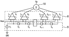
図2は、本発明の実施の形態1に係るバイアス回路を示す図である。複数のリミッタ増幅器8はそれぞれ差動入力端子を有する。複数のリミッタ増幅器8の差動入力端子の一方の端子にモニタ電圧Vmon(電源電圧)が入力される。複数の参照電圧源9が複数の差動入力端子の他方の端子にそれぞれ参照電圧V1,・・・,Vnを供給する。加算器10が複数のリミッタ増幅器8の出力を加算する。ここではn個のリミッタ増幅器を用いている。複数のリミッタ増幅器8は複数の参照電圧源9の参照電圧V1,・・・,Vnとモニタ電圧Vmonの差電圧により制御され、0からリミッティングレベルL1,・・・,Lnまでのレベルを出力する。
FIG. 2 is a diagram showing a bias circuit according to
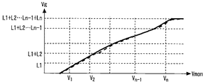
図3は、図2のバイアス回路の出力特性を示す図である。複数のリミッタ増幅器8の段数、参照電圧V1,・・・,Vn、リミッティングレベルL1,・・・,Ln、及び複数のリミッタ増幅器8の利得G1・・・Gnを適当に設定することで、モニタ電圧Vmonに対して任意の関数の出力特性を得ることができる。 FIG. 3 is a diagram showing output characteristics of the bias circuit of FIG. By appropriately setting the number of stages of the plurality of limiter amplifiers 8, reference voltages V1,..., Vn, limiting levels L1,..., Ln, and gains G1. An output characteristic of an arbitrary function can be obtained with respect to the monitor voltage Vmon.
なお、図3の出力特性は折れ線形状であるが、実際の回路では複数のリミッタ増幅器8の立ち上がり及びリミッティング特性は滑らかに立ち上がり、リミッティングされる。このため、加算器10の出力特性も折れ線ではなく滑らかになる。
Although the output characteristic of FIG. 3 is a polygonal line shape, the rising and limiting characteristics of the plurality of limiter amplifiers 8 rise smoothly and are limited in an actual circuit. For this reason, the output characteristic of the
本実施の形態ではDC−DCコンバータ5から供給される電源電圧の関数で表現される電圧をトランジスタ3のゲートに供給するバイアス回路6を用いることで、電源電圧制御範囲を大きくしつつ、電力付加効率の劣化を抑えることができる。また、電源電圧をモニタしてトランジスタ1のゲートに適切な電圧を供給するバイアス回路7を用いることで更に電力付加効率を改善することができる。なお、外部から入力した動作モード信号に応じてバイアス回路6の関数が切り替わるようにしてもよい。
In the present embodiment, by using the
実施の形態2.
図4は、本発明の実施の形態2に係るカスコード増幅器を示す図である。低域通過フィルタ11がバイアス回路6の入力とトランジスタ3のドレインの間に接続されている。また、バイアス回路7は、バイアス回路6の出力電圧の関数で表現される電圧をトランジスタ1のゲートに供給する。
FIG. 4 is a diagram showing a cascode amplifier according to
カスコード増幅器とDC−DCコンバータ5は同一チップ上に集積化することが困難なため、別チップに形成される。従って、実施の形態1では電源電圧をモニタする独立した端子が必要なため、カスコード増幅器のチップサイズの増大や、DC−DCコンバータ5を組み合わせたときの実装面積の増大の原因になる。そこで、本実施の形態ではバイアス回路6の入力をトランジスタ3のドレインに接続している。このため、端子を追加する必要が無く、チップサイズと実装面積の増大を防ぐことができる。
Since it is difficult to integrate the cascode amplifier and the DC-
また、バイアス回路7は、バイアス回路6の出力電圧の関数で表現される電圧をトランジスタ1のゲートに供給することで、バイアス回路6が複雑な関数を供給した場合でもバイアス回路7は比較的簡単なバイアス回路で構成することができる。
In addition, the
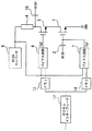
実施の形態3.
図5は、本発明の実施の形態3に係るカスコード増幅器を示す図である。デジタルインターフェース12が外部からデジタル信号を受信してデコードする。外部から入力されたデジタル情報をメモリ13,14が記憶する。バイアス回路6,7の関数はメモリ13,14に記憶されたデジタル情報に応じて設定される。これにより、変調方式の違いなどにより異なるDC−DCコンバータ5の制御条件やカスコード増幅器のバイアス条件に対し最適な条件を設定することができ、さまざまな動作条件に対し良好な電力付加効率を得ることができる。
FIG. 5 is a diagram illustrating a cascode amplifier according to
図6は、本発明の実施の形態3に係るバイアス回路を示す図である。複数のリミッタ増幅器8と複数の参照電圧源9の参照電圧Vi(i=1…n)、利得Gi(i=1…n)、及びリミッティングレベルLi(i=1…n)は可変であり、それぞれデジタル情報に応じて設定される。従って、外部からのデジタル情報に応じて任意の出力特性を得ることができる。
FIG. 6 shows a bias circuit according to
1,3 トランジスタ、4 負荷、5 DC−DCコンバータ、6,7 バイアス回路、8 リミッタ増幅器、9 参照電圧源、10 加算器、11 低域通過フィルタ、13,14 メモリ 1, 3 transistor, 4 load, 5 DC-DC converter, 6, 7 bias circuit, 8 limiter amplifier, 9 reference voltage source, 10 adder, 11 low-pass filter, 13, 14 memory
Claims (10)
ゲートと、前記第1のトランジスタの前記ドレインに接続されたソースと、ドレインとを有する第2のトランジスタと、
前記第2のトランジスタの前記ドレインに接続された負荷と、
出力電力に応じて可変な電源電圧を前記負荷を介して前記第2のトランジスタの前記ドレインに供給するDC−DCコンバータと、
前記電源電圧の関数で表現される電圧を前記第2のトランジスタの前記ゲートに供給する第1のバイアス回路と、
前記電源電圧の関数で表現される電圧を前記第1のトランジスタの前記ゲートに供給する第2のバイアス回路とを備え、
前記電源電圧が高いほど前記第2のバイアス回路の出力電圧は低くなることを特徴とするカスコード増幅器。 A first transistor having a gate to which a signal is input, a grounded source and a drain;
A second transistor having a gate, a source connected to the drain of the first transistor, and a drain;
A load connected to the drain of the second transistor;
A DC-DC converter that supplies a power supply voltage variable according to output power to the drain of the second transistor via the load;
A first bias circuit for supplying a voltage expressed as a function of the power supply voltage to the gate of the second transistor;
A second bias circuit for supplying a voltage expressed as a function of the power supply voltage to the gate of the first transistor;
It said power supply voltage is higher the second bias circuit of the output voltage characteristics and to Luke Sukodo amplifier to become lower.
ゲートと、前記第1のトランジスタの前記ドレインに接続されたソースと、ドレインとを有する第2のトランジスタと、
前記第2のトランジスタの前記ドレインに接続された負荷と、
出力電力に応じて可変な電源電圧を前記負荷を介して前記第2のトランジスタの前記ドレインに供給するDC−DCコンバータと、
前記電源電圧の関数で表現される電圧を前記第2のトランジスタの前記ゲートに供給する第1のバイアス回路と、
前記第1のバイアス回路の出力電圧の関数で表現される電圧を前記第1のトランジスタの前記ゲートに供給する第2のバイアス回路とを備えることを特徴とするカスコード増幅器。 A first transistor having a gate to which a signal is input, a grounded source and a drain;
A second transistor having a gate, a source connected to the drain of the first transistor, and a drain;
A load connected to the drain of the second transistor;
A DC-DC converter that supplies a power supply voltage variable according to output power to the drain of the second transistor via the load;
A first bias circuit for supplying a voltage expressed as a function of the power supply voltage to the gate of the second transistor;
The first bias circuit second supplying function voltage represented by the output voltage to the gate of said first transistor of the bias circuit, features and to Luke Sukodo amplifier that comprises a.
ゲートと、前記第1のトランジスタの前記ドレインに接続されたソースと、ドレインとを有する第2のトランジスタと、
前記第2のトランジスタの前記ドレインに接続された負荷と、
出力電力に応じて可変な電源電圧を前記負荷を介して前記第2のトランジスタの前記ドレインに供給するDC−DCコンバータと、
前記電源電圧の関数で表現される電圧を前記第2のトランジスタの前記ゲートに供給する第1のバイアス回路とを備え、
前記第1のバイアス回路は、前記第1のトランジスタのドレイン電圧がある一定の電圧以上にならないよう制限することを特徴とするカスコード増幅器。 A first transistor having a gate to which a signal is input, a grounded source and a drain;
A second transistor having a gate, a source connected to the drain of the first transistor, and a drain;
A load connected to the drain of the second transistor;
A DC-DC converter that supplies a power supply voltage variable according to output power to the drain of the second transistor via the load;
A first bias circuit for supplying a voltage expressed as a function of the power supply voltage to the gate of the second transistor;
The first bias circuit, the first feature and to Luke Sukodo amplifier to limit so as not to more than a predetermined voltage that the drain voltage of the transistor.
ゲートと、前記第1のトランジスタの前記ドレインに接続されたソースと、ドレインとを有する第2のトランジスタと、
前記第2のトランジスタの前記ドレインに接続された負荷と、
出力電力に応じて可変な電源電圧を前記負荷を介して前記第2のトランジスタの前記ドレインに供給するDC−DCコンバータと、
前記電源電圧の関数で表現される電圧を前記第2のトランジスタの前記ゲートに供給する第1のバイアス回路とを備え、
前記第1のバイアス回路は、前記第1のトランジスタのドレイン電圧がある一定の電圧以下にならないよう制限することを特徴とするカスコード増幅器。 A first transistor having a gate to which a signal is input, a grounded source and a drain;
A second transistor having a gate, a source connected to the drain of the first transistor, and a drain;
A load connected to the drain of the second transistor;
A DC-DC converter that supplies a power supply voltage variable according to output power to the drain of the second transistor via the load;
A first bias circuit for supplying a voltage expressed as a function of the power supply voltage to the gate of the second transistor;
The first bias circuit, the first feature and to Luke Sukodo amplifier to limit so as not to below a predetermined voltage is the drain voltage of the transistor.
ゲートと、前記第1のトランジスタの前記ドレインに接続されたソースと、ドレインとを有する第2のトランジスタと、
前記第2のトランジスタの前記ドレインに接続された負荷と、
出力電力に応じて可変な電源電圧を前記負荷を介して前記第2のトランジスタの前記ドレインに供給するDC−DCコンバータと、
前記電源電圧の関数で表現される電圧を前記第2のトランジスタの前記ゲートに供給する第1のバイアス回路とを備え、
外部から入力した動作モード信号に応じて前記第1のバイアス回路の関数が切り替わることを特徴とするカスコード増幅器。 A first transistor having a gate to which a signal is input, a grounded source and a drain;
A second transistor having a gate, a source connected to the drain of the first transistor, and a drain;
A load connected to the drain of the second transistor;
A DC-DC converter that supplies a power supply voltage variable according to output power to the drain of the second transistor via the load;
A first bias circuit for supplying a voltage expressed as a function of the power supply voltage to the gate of the second transistor;
Wherein in response to an external operation mode input from the signal first characterized in that the switching function of the bias circuit and to Luke Sukodo amplifier.
ゲートと、前記第1のトランジスタの前記ドレインに接続されたソースと、ドレインとを有する第2のトランジスタと、
前記第2のトランジスタの前記ドレインに接続された負荷と、
出力電力に応じて可変な電源電圧を前記負荷を介して前記第2のトランジスタの前記ドレインに供給するDC−DCコンバータと、
前記電源電圧の関数で表現される電圧を前記第2のトランジスタの前記ゲートに供給する第1のバイアス回路とを備え、
前記第1のバイアス回路は、
差動入力端子を有し、前記差動入力端子の一方の端子に前記電源電圧が入力される複数のリミッタ増幅器と、
前記複数のリミッタ増幅器の前記差動入力端子の他方の端子にそれぞれ参照電圧を供給する複数の参照電圧源と、
前記複数のリミッタ増幅器の出力を加算する加算器とを有することを特徴とするカスコード増幅器。 A first transistor having a gate to which a signal is input, a grounded source and a drain;
A second transistor having a gate, a source connected to the drain of the first transistor, and a drain;
A load connected to the drain of the second transistor;
A DC-DC converter for supplying a power supply voltage variable according to output power to the drain of the second transistor via the load;
A first bias circuit for supplying a voltage expressed as a function of the power supply voltage to the gate of the second transistor;
The first bias circuit includes:
A plurality of limiter amplifiers having a differential input terminal, wherein the power supply voltage is input to one terminal of the differential input terminal;
A plurality of reference voltage sources each supplying a reference voltage to the other terminal of the differential input terminals of the plurality of limiter amplifiers;
Features and to Luke Sukodo amplifier to have an adder for adding outputs of the plurality of limiting amplifier.
ゲートと、前記第1のトランジスタの前記ドレインに接続されたソースと、ドレインとを有する第2のトランジスタと、
前記第2のトランジスタの前記ドレインに接続された負荷と、
出力電力に応じて可変な電源電圧を前記負荷を介して前記第2のトランジスタの前記ドレインに供給するDC−DCコンバータと、
前記電源電圧の関数で表現される電圧を前記第2のトランジスタの前記ゲートに供給する第1のバイアス回路と、
外部から入力されたデジタル情報を記憶するメモリとを備え、
前記第1のバイアス回路の関数は前記デジタル情報に応じて設定されることを特徴とするカスコード増幅器。 A first transistor having a gate to which a signal is input, a grounded source and a drain;
A second transistor having a gate, a source connected to the drain of the first transistor, and a drain;
A load connected to the drain of the second transistor;
A DC-DC converter that supplies a power supply voltage variable according to output power to the drain of the second transistor via the load;
A first bias circuit for supplying a voltage expressed as a function of the power supply voltage to the gate of the second transistor;
And a memory for storing the digital information inputted from outside,
The first bias circuit functions features and to Luke Sukodo amplifier that is set according to the digital information.
Priority Applications (4)
| Application Number | Priority Date | Filing Date | Title |
|---|---|---|---|
| JP2013259217A JP6410007B2 (en) | 2013-12-16 | 2013-12-16 | Cascode amplifier |
| US14/462,625 US9306500B2 (en) | 2013-12-16 | 2014-08-19 | Cascode amplifier |
| KR1020140175592A KR101691456B1 (en) | 2013-12-16 | 2014-12-09 | Cascode amplifier |
| CN201410782219.1A CN104716910B (en) | 2013-12-16 | 2014-12-16 | cascode amplifier |
Applications Claiming Priority (1)
| Application Number | Priority Date | Filing Date | Title |
|---|---|---|---|
| JP2013259217A JP6410007B2 (en) | 2013-12-16 | 2013-12-16 | Cascode amplifier |
Publications (3)
| Publication Number | Publication Date |
|---|---|
| JP2015115929A JP2015115929A (en) | 2015-06-22 |
| JP2015115929A5 JP2015115929A5 (en) | 2016-11-24 |
| JP6410007B2 true JP6410007B2 (en) | 2018-10-24 |
Family
ID=53369699
Family Applications (1)
| Application Number | Title | Priority Date | Filing Date |
|---|---|---|---|
| JP2013259217A Active JP6410007B2 (en) | 2013-12-16 | 2013-12-16 | Cascode amplifier |
Country Status (4)
| Country | Link |
|---|---|
| US (1) | US9306500B2 (en) |
| JP (1) | JP6410007B2 (en) |
| KR (1) | KR101691456B1 (en) |
| CN (1) | CN104716910B (en) |
Families Citing this family (6)
| Publication number | Priority date | Publication date | Assignee | Title |
|---|---|---|---|---|
| US9455755B2 (en) | 2014-10-06 | 2016-09-27 | Skyworks Solutions, Inc. | Aggregate signal amplification device and method |
| US9496207B1 (en) | 2015-06-19 | 2016-11-15 | Semiconductor Components Industries, Llc | Cascode semiconductor package and related methods |
| CN110247552A (en) * | 2016-12-29 | 2019-09-17 | 华为技术有限公司 | A kind of DC-DC converter |
| KR102075951B1 (en) | 2017-09-29 | 2020-02-11 | 가부시키가이샤 무라타 세이사쿠쇼 | Power amplifier circuit |
| JP2021090168A (en) * | 2019-12-05 | 2021-06-10 | 株式会社村田製作所 | Power amplifier circuit |
| CN111313671B (en) * | 2020-02-18 | 2021-07-20 | 广州慧智微电子有限公司 | Integrated overvoltage protection circuit |
Family Cites Families (18)
| Publication number | Priority date | Publication date | Assignee | Title |
|---|---|---|---|---|
| JPS59228475A (en) | 1983-06-09 | 1984-12-21 | Matsushita Electric Ind Co Ltd | Video output amplifier |
| US5079515A (en) * | 1989-05-31 | 1992-01-07 | Kabushiki Kaisha Toshiba | Linearized differential amplifier |
| JP2888923B2 (en) | 1989-05-31 | 1999-05-10 | 株式会社東芝 | Linearized differential amplifier |
| JPH03240306A (en) | 1990-02-19 | 1991-10-25 | Hitachi Ltd | Cascode amplifier |
| JP3711193B2 (en) * | 1998-01-16 | 2005-10-26 | 三菱電機株式会社 | Transmission / reception switching circuit |
| JP3474825B2 (en) * | 2000-03-13 | 2003-12-08 | 富士通カンタムデバイス株式会社 | High frequency power amplifier and communication device |
| JP2003347867A (en) | 2002-05-23 | 2003-12-05 | Nec Corp | Bias setting circuit for fet |
| JP4262545B2 (en) * | 2003-07-09 | 2009-05-13 | 三菱電機株式会社 | Cascode connection circuit and integrated circuit thereof |
| JP2006197227A (en) * | 2005-01-13 | 2006-07-27 | Renesas Technology Corp | Variable gain amplifier circuit, receiver, and transmitter |
| JP2007074121A (en) * | 2005-09-05 | 2007-03-22 | Fujitsu Ltd | Amplifier and mutual conductance control method |
| JP2010068261A (en) * | 2008-09-11 | 2010-03-25 | Mitsubishi Electric Corp | Cascode circuit |
| US8385854B2 (en) | 2009-05-21 | 2013-02-26 | Qualcomm Incorporated | Adaptive parametric power amplifier protection circuit |
| CN101924520B (en) * | 2009-06-17 | 2012-11-14 | 中兴通讯股份有限公司 | Base station power amplifier and method for enhancing efficiency of base station power amplifier |
| US8150343B2 (en) * | 2009-09-21 | 2012-04-03 | Broadcom Corporation | Dynamic stability, gain, efficiency and impedance control in a linear/non-linear CMOS power amplifier |
| US8106711B2 (en) | 2009-11-12 | 2012-01-31 | Peregrine Semiconductor Coporation | Stacked pre-driver amplifier |
| WO2012164794A1 (en) | 2011-06-01 | 2012-12-06 | パナソニック株式会社 | Low-noise amplifier with through mode |
| US8665016B2 (en) * | 2012-04-30 | 2014-03-04 | Broadcom Corporation | Supply tracking |
| US9413298B2 (en) * | 2012-12-28 | 2016-08-09 | Peregrine Semiconductor Corporation | Amplifier dynamic bias adjustment for envelope tracking |
-
2013
- 2013-12-16 JP JP2013259217A patent/JP6410007B2/en active Active
-
2014
- 2014-08-19 US US14/462,625 patent/US9306500B2/en active Active
- 2014-12-09 KR KR1020140175592A patent/KR101691456B1/en active IP Right Grant
- 2014-12-16 CN CN201410782219.1A patent/CN104716910B/en active Active
Also Published As
| Publication number | Publication date |
|---|---|
| CN104716910B (en) | 2018-10-16 |
| KR20150070011A (en) | 2015-06-24 |
| US20150171794A1 (en) | 2015-06-18 |
| CN104716910A (en) | 2015-06-17 |
| US9306500B2 (en) | 2016-04-05 |
| KR101691456B1 (en) | 2016-12-30 |
| JP2015115929A (en) | 2015-06-22 |
Similar Documents
| Publication | Publication Date | Title |
|---|---|---|
| JP6410007B2 (en) | Cascode amplifier | |
| JP4330549B2 (en) | High frequency power amplifier | |
| JP5939404B2 (en) | Radio frequency amplifier circuit and power amplifier module | |
| US9876501B2 (en) | Switching power amplifier and method for controlling the switching power amplifier | |
| US8896375B2 (en) | Efficiency improved envelope amplifier using dual switching amplifiers | |
| US11038469B2 (en) | Power amplification module | |
| JP2018198355A (en) | Power amplifier circuit | |
| JP2016208305A (en) | Power Amplifier Module | |
| JP5673361B2 (en) | Power amplifier | |
| JP2016213547A (en) | Power amplification module | |
| JP2011101405A (en) | High-frequency power amplifier | |
| JP2009225342A (en) | Variable-gain low noise amplifier | |
| US8736376B2 (en) | Power amplifier module having bias circuit | |
| JP2019205006A (en) | Power amplifier circuit | |
| US20160344357A1 (en) | Power control method of amplifying module | |
| CN109586674B (en) | Power amplifying circuit | |
| US10879847B2 (en) | Transmission unit | |
| JP2007281691A (en) | Power amplifier | |
| JP2010141695A (en) | High-frequency circuit | |
| JP2006033134A (en) | High frequency power amplifier | |
| JP5355648B2 (en) | High frequency amplifier | |
| JP2009077449A (en) | High frequency power amplification device | |
| JP2006262518A (en) | High frequency power amplifier module and wireless communication apparatus | |
| JP2013106252A (en) | Transmission amplifier |
Legal Events
| Date | Code | Title | Description |
|---|---|---|---|
| A521 | Written amendment |
Free format text: JAPANESE INTERMEDIATE CODE: A523 Effective date: 20160930 |
|
| A621 | Written request for application examination |
Free format text: JAPANESE INTERMEDIATE CODE: A621 Effective date: 20160930 |
|
| A977 | Report on retrieval |
Free format text: JAPANESE INTERMEDIATE CODE: A971007 Effective date: 20171017 |
|
| A131 | Notification of reasons for refusal |
Free format text: JAPANESE INTERMEDIATE CODE: A131 Effective date: 20171114 |
|
| A601 | Written request for extension of time |
Free format text: JAPANESE INTERMEDIATE CODE: A601 Effective date: 20171213 |
|
| A521 | Written amendment |
Free format text: JAPANESE INTERMEDIATE CODE: A523 Effective date: 20180307 |
|
| A711 | Notification of change in applicant |
Free format text: JAPANESE INTERMEDIATE CODE: A711 Effective date: 20180628 |
|
| A521 | Written amendment |
Free format text: JAPANESE INTERMEDIATE CODE: A821 Effective date: 20180628 |
|
| TRDD | Decision of grant or rejection written | ||
| A01 | Written decision to grant a patent or to grant a registration (utility model) |
Free format text: JAPANESE INTERMEDIATE CODE: A01 Effective date: 20180829 |
|
| A61 | First payment of annual fees (during grant procedure) |
Free format text: JAPANESE INTERMEDIATE CODE: A61 Effective date: 20180911 |
|
| R150 | Certificate of patent or registration of utility model |
Ref document number: 6410007 Country of ref document: JP Free format text: JAPANESE INTERMEDIATE CODE: R150 |