JP6364348B2 - 2-pore device - Google Patents
2-pore device Download PDFInfo
- Publication number
- JP6364348B2 JP6364348B2 JP2014521721A JP2014521721A JP6364348B2 JP 6364348 B2 JP6364348 B2 JP 6364348B2 JP 2014521721 A JP2014521721 A JP 2014521721A JP 2014521721 A JP2014521721 A JP 2014521721A JP 6364348 B2 JP6364348 B2 JP 6364348B2
- Authority
- JP
- Japan
- Prior art keywords
- voltage
- pore
- chamber
- pores
- polynucleotide
- Prior art date
- Legal status (The legal status is an assumption and is not a legal conclusion. Google has not performed a legal analysis and makes no representation as to the accuracy of the status listed.)
- Active
Links
Images

Classifications
-
- C—CHEMISTRY; METALLURGY
- C12—BIOCHEMISTRY; BEER; SPIRITS; WINE; VINEGAR; MICROBIOLOGY; ENZYMOLOGY; MUTATION OR GENETIC ENGINEERING
- C12M—APPARATUS FOR ENZYMOLOGY OR MICROBIOLOGY; APPARATUS FOR CULTURING MICROORGANISMS FOR PRODUCING BIOMASS, FOR GROWING CELLS OR FOR OBTAINING FERMENTATION OR METABOLIC PRODUCTS, i.e. BIOREACTORS OR FERMENTERS
- C12M41/00—Means for regulation, monitoring, measurement or control, e.g. flow regulation
- C12M41/48—Automatic or computerized control
-
- G—PHYSICS
- G01—MEASURING; TESTING
- G01N—INVESTIGATING OR ANALYSING MATERIALS BY DETERMINING THEIR CHEMICAL OR PHYSICAL PROPERTIES
- G01N27/00—Investigating or analysing materials by the use of electric, electrochemical, or magnetic means
- G01N27/26—Investigating or analysing materials by the use of electric, electrochemical, or magnetic means by investigating electrochemical variables; by using electrolysis or electrophoresis
- G01N27/416—Systems
- G01N27/447—Systems using electrophoresis
- G01N27/44756—Apparatus specially adapted therefor
- G01N27/44765—Apparatus specially adapted therefor of the counter-flow type
-
- G—PHYSICS
- G01—MEASURING; TESTING
- G01N—INVESTIGATING OR ANALYSING MATERIALS BY DETERMINING THEIR CHEMICAL OR PHYSICAL PROPERTIES
- G01N33/00—Investigating or analysing materials by specific methods not covered by groups G01N1/00 - G01N31/00
- G01N33/48—Biological material, e.g. blood, urine; Haemocytometers
- G01N33/483—Physical analysis of biological material
- G01N33/487—Physical analysis of biological material of liquid biological material
- G01N33/48707—Physical analysis of biological material of liquid biological material by electrical means
- G01N33/48721—Investigating individual macromolecules, e.g. by translocation through nanopores
-
- C—CHEMISTRY; METALLURGY
- C12—BIOCHEMISTRY; BEER; SPIRITS; WINE; VINEGAR; MICROBIOLOGY; ENZYMOLOGY; MUTATION OR GENETIC ENGINEERING
- C12M—APPARATUS FOR ENZYMOLOGY OR MICROBIOLOGY; APPARATUS FOR CULTURING MICROORGANISMS FOR PRODUCING BIOMASS, FOR GROWING CELLS OR FOR OBTAINING FERMENTATION OR METABOLIC PRODUCTS, i.e. BIOREACTORS OR FERMENTERS
- C12M41/00—Means for regulation, monitoring, measurement or control, e.g. flow regulation
- C12M41/46—Means for regulation, monitoring, measurement or control, e.g. flow regulation of cellular or enzymatic activity or functionality, e.g. cell viability
-
- C—CHEMISTRY; METALLURGY
- C12—BIOCHEMISTRY; BEER; SPIRITS; WINE; VINEGAR; MICROBIOLOGY; ENZYMOLOGY; MUTATION OR GENETIC ENGINEERING
- C12Q—MEASURING OR TESTING PROCESSES INVOLVING ENZYMES, NUCLEIC ACIDS OR MICROORGANISMS; COMPOSITIONS OR TEST PAPERS THEREFOR; PROCESSES OF PREPARING SUCH COMPOSITIONS; CONDITION-RESPONSIVE CONTROL IN MICROBIOLOGICAL OR ENZYMOLOGICAL PROCESSES
- C12Q1/00—Measuring or testing processes involving enzymes, nucleic acids or microorganisms; Compositions therefor; Processes of preparing such compositions
- C12Q1/68—Measuring or testing processes involving enzymes, nucleic acids or microorganisms; Compositions therefor; Processes of preparing such compositions involving nucleic acids
- C12Q1/6869—Methods for sequencing
-
- G—PHYSICS
- G01—MEASURING; TESTING
- G01N—INVESTIGATING OR ANALYSING MATERIALS BY DETERMINING THEIR CHEMICAL OR PHYSICAL PROPERTIES
- G01N27/00—Investigating or analysing materials by the use of electric, electrochemical, or magnetic means
- G01N27/26—Investigating or analysing materials by the use of electric, electrochemical, or magnetic means by investigating electrochemical variables; by using electrolysis or electrophoresis
- G01N27/416—Systems
- G01N27/447—Systems using electrophoresis
- G01N27/44704—Details; Accessories
- G01N27/44713—Particularly adapted electric power supply
-
- G—PHYSICS
- G01—MEASURING; TESTING
- G01N—INVESTIGATING OR ANALYSING MATERIALS BY DETERMINING THEIR CHEMICAL OR PHYSICAL PROPERTIES
- G01N27/00—Investigating or analysing materials by the use of electric, electrochemical, or magnetic means
- G01N27/26—Investigating or analysing materials by the use of electric, electrochemical, or magnetic means by investigating electrochemical variables; by using electrolysis or electrophoresis
- G01N27/416—Systems
- G01N27/447—Systems using electrophoresis
- G01N27/44704—Details; Accessories
- G01N27/44717—Arrangements for investigating the separated zones, e.g. localising zones
- G01N27/4473—Arrangements for investigating the separated zones, e.g. localising zones by electric means
-
- G—PHYSICS
- G01—MEASURING; TESTING
- G01N—INVESTIGATING OR ANALYSING MATERIALS BY DETERMINING THEIR CHEMICAL OR PHYSICAL PROPERTIES
- G01N27/00—Investigating or analysing materials by the use of electric, electrochemical, or magnetic means
- G01N27/26—Investigating or analysing materials by the use of electric, electrochemical, or magnetic means by investigating electrochemical variables; by using electrolysis or electrophoresis
- G01N27/416—Systems
- G01N27/447—Systems using electrophoresis
- G01N27/44704—Details; Accessories
- G01N27/44743—Introducing samples
-
- G—PHYSICS
- G01—MEASURING; TESTING
- G01N—INVESTIGATING OR ANALYSING MATERIALS BY DETERMINING THEIR CHEMICAL OR PHYSICAL PROPERTIES
- G01N27/00—Investigating or analysing materials by the use of electric, electrochemical, or magnetic means
- G01N27/26—Investigating or analysing materials by the use of electric, electrochemical, or magnetic means by investigating electrochemical variables; by using electrolysis or electrophoresis
- G01N27/416—Systems
- G01N27/447—Systems using electrophoresis
- G01N27/44756—Apparatus specially adapted therefor
- G01N27/44791—Microapparatus
-
- B—PERFORMING OPERATIONS; TRANSPORTING
- B82—NANOTECHNOLOGY
- B82Y—SPECIFIC USES OR APPLICATIONS OF NANOSTRUCTURES; MEASUREMENT OR ANALYSIS OF NANOSTRUCTURES; MANUFACTURE OR TREATMENT OF NANOSTRUCTURES
- B82Y30/00—Nanotechnology for materials or surface science, e.g. nanocomposites
Description
(関連出願のクロスリファレンス)
本願は、2011年7月20日に出願した米国仮特許出願番号第61/572,843号の米国特許法第119(e)条に基づく優先権を主張し、その内容は本願において援用する。
(Cross-reference of related applications)
This application claims priority under US Patent Act 119 (e) of US Provisional Patent Application No. 61 / 572,843, filed July 20, 2011, the contents of which are incorporated herein by reference.
ナノ細孔はナノスケールの開口部であり、脂質膜(生体細孔)におけるタンパクチャネルとして自然に形成し、あるいは固体の基板において開口部(固体の細孔)を穿孔またはエッチングすることによって作られる。係るナノ細孔がこのナノ細孔によって分離される2つのチャンバを備えるナノデバイス内に組み込まれると、高感度のパッチクランプ増幅器が、膜電圧を印加して細孔を通してイオン電流を測定するのに使用することができる。 Nanopores are nanoscale openings that are formed naturally as protein channels in lipid membranes (biological pores), or created by drilling or etching openings (solid pores) in a solid substrate. . When such a nanopore is incorporated into a nanodevice comprising two chambers separated by the nanopore, a highly sensitive patch clamp amplifier applies a membrane voltage to measure the ionic current through the pore. Can be used.
ナノ細孔は廉価な全ゲノムDNAシークエンシングに対して成功を約束するものである。この点に関し、個々のDNA分子は電気泳動によって細孔を通して捕捉され駆動されることができ、各捕捉事象はイオン電流において一時的な移動として検出される。次にDNA分子のシークエンスは、移動されたイオン電流の記録内のパターンから推測することができ、DNAが細孔チャネルを通過する際にナノ細孔内またはナノ細孔近くの他の補助的なセンサーから推測することができる。 Nanopores promise success for inexpensive whole-genome DNA sequencing. In this regard, individual DNA molecules can be captured and driven through the pores by electrophoresis, and each capture event is detected as a transient movement in the ionic current. The sequence of the DNA molecule can then be inferred from the pattern in the transferred ionic current record, and other ancillary in or near the nanopore as the DNA passes through the pore channel. Can be inferred from the sensor.
原理上としては、ナノ細孔シークエンサーはサンプル増幅の必要性をなくすことができ、シークエンシング動作中に触媒決定のために使用される酵素および試薬の使用をなくすことができ、シークエンシング進捗の検出のためのオプティクスをなくすことができ、これらのいくつかまたは全ては従来のシークエンシング・バイ・シンセシス(合成によるシークエンシング)法によって必要とされる。 In principle, nanopore sequencers can eliminate the need for sample amplification, can eliminate the use of enzymes and reagents used for catalyst determination during sequencing operations, and detect sequencing progress. Optics, and some or all of these are required by conventional sequencing-by-synthesis methods.
ナノ細孔センサーは純粋に電気的なものであり、血液または唾液試料から得られるものよりも大きくはない濃度/体積におけるDNAを検出することができる。更に、ナノ細孔はシークエンシングされたDNAの読み出し長さ(read−length)を450ベースから10,000ベース以上まで劇的に増加する。 Nanopore sensors are purely electrical and can detect DNA at concentrations / volumes not greater than those obtained from blood or saliva samples. Furthermore, nanopores dramatically increase the read-length of sequenced DNA from 450 bases to over 10,000 bases.
ナノ細孔シークエンシングに対する2つの主な障害があり、それは(1)デノボシークエンシングのための核酸における各ヌクレオチドの特定を正確に決定するのに十分な感度の欠如(単一ヌクレオチド感度の欠如),および(2)検出中にナノ細孔を通して各ヌクレオチドユニットの送出速度を制御する能力である。多くの研究グループが障害1に対処するためにナノ細孔を開発および改良しているが、酵素またはオプティクスの使用を伴わない障害2に対処する方法がなく、酵素またはオプティクスの使用は、特化されたナノ細孔技術においてのみ効果があり、純粋な電気的方法と比較してより複雑かつコストが高い。
There are two main obstacles to nanopore sequencing: (1) lack of sensitivity sufficient to accurately determine the identity of each nucleotide in the nucleic acid for de novo sequencing (lack of single nucleotide sensitivity) , And (2) the ability to control the delivery rate of each nucleotide unit through the nanopore during detection. Many research groups have developed and improved nanopores to address
一実施形態において、上部チャンバ、中間チャンバおよび下部チャンバを備える装置であって、前記上部チャンバは第1の細孔を通して前記中間チャンバと連通し、前記中間チャンバは第2の細孔を通して前記下部チャンバと連通し、前記第1の細孔および第2の細孔は直径約1nm〜約100nmであり、互いから約10nm〜約1000nm離れており、前記チャンバのそれぞれは、電源に接続するための電極を備える、装置が提供される。 In one embodiment, an apparatus comprising an upper chamber, an intermediate chamber, and a lower chamber, wherein the upper chamber communicates with the intermediate chamber through a first pore, and the intermediate chamber passes through a second pore. The first pore and the second pore are about 1 nm to about 100 nm in diameter and about 10 nm to about 1000 nm apart from each other, each of the chambers having an electrode for connection to a power source An apparatus is provided comprising:
一の態様において、第1のおよび第2の細孔は実質的に同軸である。 In one embodiment, the first and second pores are substantially coaxial.
一の態様において、この装置は、ケイ素,窒化ケイ素,二酸化ケイ素,グラフェン,カーボンナノチューブ,TiO2,HfO2,Al2O3,金属層,ガラス,生体ナノ細孔,生体細孔挿入物を備える膜,およびこれらの組み合わせからなる群から選択される材料を含む。 In one embodiment, the device comprises silicon, silicon nitride, silicon dioxide, graphene, carbon nanotubes, TiO 2 , HfO 2 , Al 2 O 3 , metal layer, glass, bio-nanopore, biopore insert. Including a material selected from the group consisting of a membrane, and combinations thereof.
一の態様において、前記第1の細孔および前記第2の細孔は深さ約0.3nm〜約100nmである。 In one embodiment, the first pore and the second pore are about 0.3 nm to about 100 nm in depth.
一の態様において、前記電源は、前記上部チャンバと前記中間チャンバとの間に第1の電圧と、前記中間チャンバと前記下部チャンバとの間に第2の電圧と、を提供するように構成され、前記第1の電圧および前記第2の電圧は独立して調節可能である。 In one aspect, the power source is configured to provide a first voltage between the upper chamber and the middle chamber and a second voltage between the middle chamber and the lower chamber. The first voltage and the second voltage can be adjusted independently.
一の態様において、この電源は、前記第1の電圧および第2の電圧のそれぞれを生成するために電圧クランプシステムまたはパッチクランプシステムを備える。一の態様において、この中間チャンバは前記2つの電圧に対して接地するように調節される。一の態様において、この中間チャンバは、この中間チャンバ内の前記細孔のそれぞれと前記電極との間に伝導性を提供するための媒体を備える。 In one aspect, the power supply includes a voltage clamp system or a patch clamp system to generate each of the first voltage and the second voltage. In one embodiment, the intermediate chamber is adjusted to ground for the two voltages. In one aspect, the intermediate chamber comprises a medium for providing conductivity between each of the pores in the intermediate chamber and the electrode.
いくつかの態様において、この電源(例えば電圧クランプシステムまたはパッチクランプシステム)は更に、前記細孔のそれぞれを通して前記イオン電流を測定するように構成される。 In some embodiments, the power source (eg, voltage clamp system or patch clamp system) is further configured to measure the ion current through each of the pores.
別の実施形態は、上部チャンバ、中間チャンバおよび下部チャンバを備える装置であって、前記上部チャンバは、第1の細孔を通して前記中間チャンバと連通し、前記中間チャンバは第2の細孔を通して前記下部チャンバと連通し、前記第1の細孔および第2の細孔は直径約1nm〜約100nmであり、互いから約10nm〜約1000nm離れており、前記細孔のそれぞれに電圧を印加するために電圧クランプまたはパッチクランプシステムに接続して前記細孔のそれぞれを通してイオンを測定するための前記チャンバのそれぞれにある電極を備え、前記中間チャンバ内の前記電極は前記2つの電圧クランプまたはパッチクランプシステムの共通するアースに接続される、装置を提供する。 Another embodiment is an apparatus comprising an upper chamber, an intermediate chamber, and a lower chamber, wherein the upper chamber communicates with the intermediate chamber through a first pore, and the intermediate chamber passes through a second pore. In communication with the lower chamber, the first and second pores are about 1 nm to about 100 nm in diameter and are about 10 nm to about 1000 nm away from each other to apply a voltage to each of the pores An electrode in each of the chambers for measuring ions through each of the pores connected to a voltage clamp or patch clamp system, the electrodes in the intermediate chamber comprising the two voltage clamp or patch clamp systems The device is connected to a common ground.
更に、一実施形態において、細孔を通る荷電ポリマーの移動を制御する方法であって、
(a)荷電ポリマーを含むサンプルを上記実施形態のいずれかに記載の装置の前記上部チャンバ、中間チャンバまたは下部チャンバの一つに装填するステップを備え、ここで、前記装置は前記上部チャンバと前記中間チャンバとの間の第1の電圧、ならびに前記中間チャンバと前記下部チャンバとの間の第2の電圧を提供するための電圧クランプまたはパッチクランプシステムに接続され、(b)前記ポリマーが前記チャンバ間を移動するように初期の第1の電圧および初期の第2の電圧を設定するステップを備え、これにより、前記第1の細孔および第2の細孔の両方に亘って前記ポリマーを配置し、(c)両方の電圧が前記荷電ポリマーを前記中間チャンバから引き離すための力を生成するように第1の電圧および第2の電圧を調節するステップを備え、ここで、前記荷電ポリマーが一方向にかつ制御された方法で両方の細孔に亘って移動するように前記2つの電圧は制御された条件下で強度が異なる、方法が提供される。
Furthermore, in one embodiment, a method for controlling the movement of a charged polymer through a pore comprising:
(A) loading a sample comprising a charged polymer into one of the upper, middle or lower chambers of the apparatus according to any of the preceding embodiments, wherein the apparatus comprises the upper chamber and the Connected to a voltage clamp or patch clamp system for providing a first voltage between the intermediate chamber and a second voltage between the intermediate chamber and the lower chamber; and (b) the polymer is in the chamber Setting an initial first voltage and an initial second voltage to move between, thereby disposing the polymer across both the first and second pores And (c) adjusting the first voltage and the second voltage such that both voltages generate a force to pull the charged polymer away from the intermediate chamber. A method is provided wherein the two voltages have different intensities under controlled conditions so that the charged polymer moves across both pores in one direction and in a controlled manner. The
一の態様において、送出の制御された方法は、第1のもしくは第2の電圧または両方の電圧のアクティブ制御またはフィードバック制御によって設定され、そのいずれかまたは両方が第1のもしくは第2のイオン電流測定または両方のイオン電流測定のフィードバック関数としてである。非限定的な実施例は、第2の電圧を一定に維持し、いずれかの方向に荷電ポリマーの設定されたコントロールド・デリバリーに対して第1の電圧のフィードバックまたはアクティブ制御のためのフィードバックとして第2のイオン電流を使用することを含む。従って、一の態様において、第1の電圧は第2の細孔にて測定されたイオン電流に基づき調節される。 In one aspect, the controlled method of delivery is set by active control or feedback control of the first or second voltage or both voltages, either or both of which is the first or second ion current. As a feedback function of the measurement or both ion current measurements. A non-limiting example is to keep the second voltage constant and as feedback for the first voltage or active control for the controlled delivery of the charged polymer in either direction. Using a second ionic current. Thus, in one aspect, the first voltage is adjusted based on the ionic current measured at the second pore.
一の態様において、このサンプルは前記上部チャンバ内に装填され、前記初期の第1の電圧は前記荷電ポリマーを前記上部チャンバから前記中間チャンバへ引っ張るように設定され、前記初期の第2の電圧は前記荷電ポリマーを前記中間チャンバから前記下部チャンバへ引っ張るように設定される。 In one embodiment, the sample is loaded into the upper chamber, the initial first voltage is set to pull the charged polymer from the upper chamber to the intermediate chamber, and the initial second voltage is It is set to pull the charged polymer from the intermediate chamber to the lower chamber.
別の態様において、前記サンプルは前記中間チャンバ内に装填され、前記初期の第1の電圧は前記荷電ポリマーを前記中間チャンバから前記上部チャンバへ引っ張るように設定され、前記初期の第2の電圧は前記荷電ポリマーを前記中間チャンバから前記下部チャンバへ引っ張るように設定される。 In another aspect, the sample is loaded into the intermediate chamber, the initial first voltage is set to pull the charged polymer from the intermediate chamber to the upper chamber, and the initial second voltage is It is set to pull the charged polymer from the intermediate chamber to the lower chamber.
一の態様において、この荷電ポリマーは、ポリヌクレオチドまたはポリペプチドである。一の態様において、この荷電ポリマーはポリヌクレオチドであり、例えば、ポリヌクレオチドは、二本鎖DNA,一本鎖DNA,二本鎖RNA,一本鎖RNA,およびDNA−RNA混成物である(これらに限定されない)。 In one embodiment, the charged polymer is a polynucleotide or polypeptide. In one embodiment, the charged polymer is a polynucleotide, eg, the polynucleotide is a double stranded DNA, a single stranded DNA, a double stranded RNA, a single stranded RNA, and a DNA-RNA hybrid (these Not limited to).
一の態様において、ステップ(c)における前記調節された第1の電圧および第2の電圧は、前記2つの電圧間の強度の相違よりも約10倍〜約10,000倍高い。 In one aspect, the adjusted first and second voltages in step (c) are about 10 to about 10,000 times higher than the intensity difference between the two voltages.
一の態様において、この方法は更に、前記ポリマーのモノマー単位を特定するステップを更に備え、これは前記モノマー単位が前記細孔の一つを通過するときに当該細孔に亘るイオン電流を測定することによってなされる。一の態様において、このモノマー単位はヌクレオチドである。別の態様において、このモノマー単位はヌクレオチド対である。いくつかの態様において、単一ヌクレオチドおよびヌクレオチド対は、一の分子において検出され得る。例えば、係る分子は、より長いポリヌクレオチドあるいは一本鎖ポリヌクレオチドにおいて二重部位を有することができ、この二重部位は、ワトソン・クリックの相補的塩基対合によって部分的または完全に形成される。 In one embodiment, the method further comprises identifying a monomer unit of the polymer, which measures an ionic current across the pore as the monomer unit passes through one of the pores. Is made by In one embodiment, the monomer unit is a nucleotide. In another embodiment, the monomer units are nucleotide pairs. In some embodiments, single nucleotides and nucleotide pairs can be detected in a single molecule. For example, such a molecule can have a double site in a longer or single stranded polynucleotide, which is partially or fully formed by Watson-Crick complementary base pairing. .
一の態様において、このモノマーは、DNA結合タンパクまたはナノ粒子といった分子に結合される。DNA結合タンパクの非限定的な例は、RecAおよび配列特異的なDNA結合タンパクを含む(例えば、ラムダファージ・リプレッサー、NF−κBおよびp53)。ナノ粒子の非限定的な例は、量子ドットおよび蛍光標識を含む。 In one embodiment, the monomer is bound to a molecule such as a DNA binding protein or nanoparticle. Non-limiting examples of DNA binding proteins include RecA and sequence specific DNA binding proteins (eg, lambda phage repressor, NF-κB and p53). Non-limiting examples of nanoparticles include quantum dots and fluorescent labels.
一の態様において、このポリマーはその一端部でビード(bead)といった固体支持体に接合される。 In one embodiment, the polymer is bonded at one end to a solid support such as a bead.
更に別の実施形態は、ポリヌクレオチドのシークエンスを決定するための方法であって、(a) ポリヌクレオチドを含むサンプルを上記実施形態のいずれかに記載の前記装置の前記上部チャンバ内に装填するステップを備え、前記装置は前記上部チャンバと前記中間チャンバとの間の第1の電圧、ならびに前記中間チャンバと前記下部チャンバとの間の第2の電圧を提供するための電圧クランプまたはパッチクランプシステムに接続され、前記ポリヌクレオチドは当該ポリヌクレオチドの一端にて固体支持体に任意に接着され、(b) 前記ポリヌクレオチドが前記上部チャンバから前記中間チャンバへおよび前記中間チャンバから前記下部チャンバへ移動するように初期の第1の電圧および初期の第2の電圧を設定するステップを備え、これにより、前記第1の細孔および第2の細孔の両方に亘って前記ポリマーを配置し、(c) 両方の電圧が前記ポリヌクレオチドを前記中間チャンバから引き離すための力を生成するように第1の電圧および第2の電圧を調節するステップを備え、ここで、前記ポリヌクレオチドが一方向にかつ制御された方法で両方の細孔に亘って移動するように前記2つの電圧は制御された条件下で強度が異なり、(d) 前記細孔の一方を通る前記ポリヌクレオチドの各ヌクレオチドを特定するステップを更に備え、これは前記ヌクレオチドが当該細孔を通過するときに当該細孔に亘るイオン電流を測定することによってなさる、方法を提供する。 Yet another embodiment is a method for determining a sequence of a polynucleotide, comprising: (a) loading a sample containing the polynucleotide into the upper chamber of the apparatus according to any of the previous embodiments. The apparatus includes: a voltage clamp or patch clamp system for providing a first voltage between the upper chamber and the middle chamber, and a second voltage between the middle chamber and the lower chamber; Connected, and the polynucleotide is optionally adhered to a solid support at one end of the polynucleotide, (b) such that the polynucleotide moves from the upper chamber to the intermediate chamber and from the intermediate chamber to the lower chamber. A step of setting an initial first voltage and an initial second voltage. This places the polymer across both the first and second pores, and (c) both voltages generate a force to pull the polynucleotide away from the intermediate chamber. Adjusting the first voltage and the second voltage, wherein the two voltages are controlled such that the polynucleotide moves across both pores in one direction and in a controlled manner. And (d) identifying each nucleotide of the polynucleotide that passes through one of the pores, which spans the pore as the nucleotide passes through the pore. A method is provided that is accomplished by measuring an ionic current.
添付の図面は例示のみを目的として実施形態を記載している。 The accompanying drawings describe embodiments for purposes of illustration only.
図のいくつかまたは全ては例示的な概略図であり、図示された要素の実際の相対的サイズまたは位置を表しているわけではない。これらの図は一または複数の実施形態を示す目的で表されており、後述の特許請求の範囲または請求項の意味を限定するために用いられるものではないことは容易に理解されよう。 Some or all of the figures are exemplary schematics and do not represent the actual relative sizes or positions of the illustrated elements. It should be readily understood that these drawings are presented for the purpose of illustrating one or more embodiments and are not intended to limit the meaning of the claims or the claims below.
本願全体を通して,その記載内容は本発明の装置および方法の様々な実施形態を参照する。説明する様々な実施形態は様々な説明上の例を提供するものとして意図し、種発明を記載するものとして理解されるべきではない。様々な実施形態の説明は本明細書においてその範囲が重複し得ることに留意されたい。本明細書において記載された実施形態は単に例示的なものであり、本発明の範囲を限定することを意図していない。 Throughout this application, the description refers to various embodiments of the apparatus and method of the present invention. The various described embodiments are intended to provide various illustrative examples and should not be understood as describing the seed invention. It should be noted that the description of the various embodiments can overlap in scope herein. The embodiments described herein are merely exemplary and are not intended to limit the scope of the invention.
更に、本明細書の全体を通して、様々な文献、特許および公開公報が引用によって参照される。これらの文献、特許および公開公報の開示内容は本発明に関する技術を完全に記載するために本明細書に参照により組み込まれる。 Further, throughout this specification, various documents, patents and publications are referenced by citation. The disclosures of these documents, patents and publications are incorporated herein by reference in order to fully describe the technology relating to the present invention.
明細書および特許請求の範囲に使用される、単数「a」,「an」および「the」は文脈から明確である場合を除き、複数も含む。例えば、用語「an 電極」は複数の電極も含む。 As used in the specification and claims, the singular forms “a”, “an”, and “the” include the plural unless the context clearly dictates otherwise. For example, the term “an electrode” includes a plurality of electrodes.
本明細書において使用される用語「備える・含む」は装置および方法が、記載された部品またはステップを含むが他のものを排除するものではない。「から実質的になる」は、装置および方法を特定するのに使用される場合、その組み合わせに対して本質的な意義を有する他の部品またはステップを排除することを意味する。「のみからなる」は、他の部品またはステップを排除することを意味する。これらの移行用語のそれぞれによって定義された実施形態は本発明の範囲内である。 As used herein, the term “comprising” includes, but does not exclude, the apparatus and methods including the described parts or steps. “Consisting essentially of” when used to identify devices and methods, means excluding other parts or steps that have a substantial significance to the combination. “Comprising only” means excluding other parts or steps. Embodiments defined by each of these transition terms are within the scope of this invention.
全ての数字表示、例えば、距離,サイズ,温度,時間,電圧および濃度(範囲を含む)は、0.1単位でプラスまたはマイナスに変化する近似値である。必ずしも明確には記載していないが、全ての数字表示は「約」という文言が前に付くと理解されたい。更に、必ずしも明確には記載していないが、本明細書において記載された部品は単に例であり、係る均等物も当該技術分野において知られている。
2細孔装置(Two−Pore Device)
All numerical representations, such as distance, size, temperature, time, voltage and concentration (including range) are approximate values that change positively or negatively by 0.1 units. Although not necessarily clearly described, it is to be understood that all numeric designations are preceded by the word “about”. Further, although not necessarily explicitly described, the components described herein are merely examples, and such equivalents are known in the art.
Two-pore device (Two-Pore Device)
本発明の一実施形態は、2細孔装置を提供する。この装置は、3つのチャンバと、これらのチャンバ間の流体連通を可能にする2つの細孔とを含む。更に、各チャンバは別個の電圧をチャンバ間の各細孔に設定することができるように電源に接続するための電極を含む。 One embodiment of the present invention provides a two-pore device. The device includes three chambers and two pores that allow fluid communication between the chambers. In addition, each chamber includes an electrode for connecting to a power source so that a separate voltage can be set for each pore between the chambers.
本発明の一実施形態によると、上部チャンバ,中間チャンバおよび下部チャンバを備える装置が提供され、上部チャンバは第1の細孔を通して中間チャンバと連通し、中間チャンバは第2の細孔を通して下部チャンバと連通し、第1の細孔および第2の細孔は直径約1nm〜約100nmであり、互いから約10nm〜約1000nm離れており、更に、各チャンバは電源に接続するための電極を備える。 According to one embodiment of the present invention, an apparatus is provided comprising an upper chamber, an intermediate chamber, and a lower chamber, the upper chamber communicating with the intermediate chamber through the first pore, the intermediate chamber passing through the second pore The first and second pores are about 1 nm to about 100 nm in diameter and are about 10 nm to about 1000 nm apart from each other, and each chamber further comprises an electrode for connection to a power source .
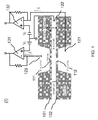
図1(1)を参照すると、この装置は上部チャンバ(チャンバA),中間チャンバ(チャンバB),および下部チャンバ(チャンバC)を含む。このチャンバは、別個の細孔(111および112)をそれぞれ有する2つの別個の層または膜(101および102)によって分離される。更に、各チャンバは電源に接続するために電極(121,122および123)を有する。上部,中間および下部チャンバの表示は相対的な文言であり、例えば、上部チャンバが地面に対して中間または下部チャンバの上にあることを意味し、その逆も然りであることは明らかである。 Referring to FIG. 1 (1), the apparatus includes an upper chamber (chamber A), an intermediate chamber (chamber B), and a lower chamber (chamber C). This chamber is separated by two separate layers or membranes (101 and 102), each having separate pores (111 and 112). In addition, each chamber has electrodes (121, 122 and 123) for connection to a power source. The upper, middle and lower chamber designations are relative terms, for example, meaning that the upper chamber is above the middle or lower chamber with respect to the ground, and vice versa .
各細孔(111および112)は大小の分子または微生物が通過できるサイズを独立して有する。一の態様において、各細孔は少なくとも直径約1nmである。あるいは、各細孔は少なくとも直径約2nm,3nm,4nm,5nm,6nm,7nm,8nm,9nm,10nm,11nm,12nm,13nm,14nm,15nm,16nm,17nm,18nm,19nm,20nm,25nm,30nm,35nm,40nm,45nm,50nm,60nm,70nm,80nm,90nmまたは100nmである。 Each pore (111 and 112) has an independent size through which large and small molecules or microorganisms can pass. In one embodiment, each pore is at least about 1 nm in diameter. Alternatively, each pore has a diameter of at least about 2 nm, 3 nm, 4 nm, 5 nm, 6 nm, 7 nm, 8 nm, 9 nm, 10 nm, 11 nm, 12 nm, 13 nm, 14 nm, 15 nm, 16 nm, 17 nm, 18 nm, 19 nm, 20 nm, 25 nm, 30 nm. , 35 nm, 40 nm, 45 nm, 50 nm, 60 nm, 70 nm, 80 nm, 90 nm or 100 nm.
一の態様において、この細孔は直径約100nm以下である。あるいは、この細孔は直径約95nm,90nm,85nm,80nm,75nm,70nm,65nm,60nm,55nm,50nm,45nm,40nm,35nm,30nm,25nm,20nm,15または10nm以下である。 In one embodiment, the pore is about 100 nm or less in diameter. Alternatively, the pore has a diameter of about 95 nm, 90 nm, 85 nm, 80 nm, 75 nm, 70 nm, 65 nm, 60 nm, 55 nm, 50 nm, 45 nm, 40 nm, 35 nm, 30 nm, 25 nm, 20 nm, 15 or 10 nm or less.
一の態様において、この細孔は直径が約1nm〜約100nmの間、または約2nm〜約80nmの間、または約3nm〜約70nmの間、または約4nm〜約60nmの間、または約5nm〜約50nmの間、または約10nm〜約40nmの間、または約15nm〜約30nmの間である。 In one embodiment, the pore has a diameter between about 1 nm and about 100 nm, or between about 2 nm and about 80 nm, or between about 3 nm and about 70 nm, or between about 4 nm and about 60 nm, or between about 5 nm and Between about 50 nm, or between about 10 nm and about 40 nm, or between about 15 nm and about 30 nm.
いくつかの態様において、細孔は実質的に円形を有する。本明細書において使用される「実質的に円形」は少なくとも約80または90%の円筒形を指す。いくつかの実施形態において、細孔は方形、矩形、三角形、楕円または六角形である。 In some embodiments, the pores have a substantially circular shape. As used herein, “substantially circular” refers to a cylindrical shape of at least about 80 or 90%. In some embodiments, the pores are square, rectangular, triangular, elliptical or hexagonal.
各細孔(111および112)はある深さを独立して有する。一の態様において、各細孔は深さが少なくとも約0.3nmである。あるいは、各細孔は深さが少なくとも約0.6nm,1nm,2nm,3nm,4nm,5nm,6nm,7nm,8nm,9nm,10nm,11nm,12nm,13nm,14nm,15nm,16nm,17nm,18nm,19nm,20nm,25nm,30nm,35nm,40nm,45nm,50nm,60nm,70nm,80nm,または90nmである。 Each pore (111 and 112) has a certain depth independently. In one embodiment, each pore is at least about 0.3 nm deep. Alternatively, each pore has a depth of at least about 0.6 nm, 1 nm, 2 nm, 3 nm, 4 nm, 5 nm, 6 nm, 7 nm, 8 nm, 9 nm, 10 nm, 11 nm, 12 nm, 13 nm, 14 nm, 15 nm, 16 nm, 17 nm, 18 nm. , 19 nm, 20 nm, 25 nm, 30 nm, 35 nm, 40 nm, 45 nm, 50 nm, 60 nm, 70 nm, 80 nm, or 90 nm.
一の態様において、各細孔は深さが約100nm以下である。あるいは、深さは約95nm,90nm,85nm,80nm,75nm,70nm,25nm,65nm,60nm,55nm,50nm,45nm,40nm,35nm,30nm,25nm,20nm,15または10nm以下である。 In one embodiment, each pore is about 100 nm or less in depth. Alternatively, the depth is about 95 nm, 90 nm, 85 nm, 80 nm, 75 nm, 70 nm, 25 nm, 65 nm, 60 nm, 55 nm, 50 nm, 45 nm, 40 nm, 35 nm, 30 nm, 25 nm, 20 nm, 15 or 10 nm or less.
一の態様において、この細孔は深さが約1nm〜約100nmの間であり、または約2nm〜約80nmの間であり、約3nm〜約70nmの間であり、または約4nm〜約60nmの間であり、約5nm〜約50nmの間であり、または約10nm〜約40nmの間であり、または約15nm〜約30nmの間である。 In one embodiment, the pore is between about 1 nm and about 100 nm in depth, or between about 2 nm and about 80 nm, between about 3 nm and about 70 nm, or between about 4 nm and about 60 nm. Between about 5 nm and about 50 nm, or between about 10 nm and about 40 nm, or between about 15 nm and about 30 nm.
一の態様において、この細孔は距離が約10nm〜約1000nmの間の分だけ離れている。一の態様において、この距離は少なくとも約10nm,または少なくとも約20nm,30nm,40nm,50nm,60nm,70nm,80nm,90nm,100nm,150nm,200nm,250nm,または300nmである。別の態様において、この距離は約1000nm,900nm,800nm,700nm,600nm,500nm,400nm,300nm,250nm,200nm,150nm,または100nm以下である。更に別の態様において、この距離は、約20nm〜約800nmの間か、約30nm〜約700nmの間か、約40nm〜約500nmの間か、約50nm〜約300nmの間である。 In one embodiment, the pores are separated by a distance between about 10 nm and about 1000 nm. In one embodiment, the distance is at least about 10 nm, or at least about 20 nm, 30 nm, 40 nm, 50 nm, 60 nm, 70 nm, 80 nm, 90 nm, 100 nm, 150 nm, 200 nm, 250 nm, or 300 nm. In another embodiment, the distance is about 1000 nm, 900 nm, 800 nm, 700 nm, 600 nm, 500 nm, 400 nm, 300 nm, 250 nm, 200 nm, 150 nm, or 100 nm or less. In yet another aspect, the distance is between about 20 nm to about 800 nm, between about 30 nm to about 700 nm, between about 40 nm to about 500 nm, or between about 50 nm to about 300 nm.
これら2つの細孔はチャンバ間の流体連通を可能にする限り任意の位置に配置されることができ、所定の大きさを有し、かつそれらの間に所定の距離を有する。一の態様において、この細孔は、それらの間に直接障害物がないように配置される。更に、一の態様において、これらの細孔は実質的は図1(1)に示されるように同軸である。 These two pores can be placed anywhere as long as they allow fluid communication between the chambers, have a predetermined size, and have a predetermined distance between them. In one embodiment, the pores are positioned so that there are no obstructions directly between them. Further, in one embodiment, these pores are substantially coaxial as shown in FIG. 1 (1).
一の態様において、この装置はチャンバ内の電極を通して一または複数の電源に接続される。いくつかの態様において、この電源は各細孔に電圧を供給するための電圧クランプまたはパッチクランプを備え、これは各細孔を通して電流を独立して測定することもできる。この点に関して、この電源は中間チャンバを両方の電圧源のための共通の接地(アース)に設定する。一の態様において、この電源は、上部チャンバ(例えば、図1(1)におけるチャンバA)と中間チャンバ(例えば、図1(1)におけるチャンバB)の間の第1の電圧を提供し、かつ中間チャンバと下部チャンバ(例えば、図1(1)におけるチャンバC)との間の第2の電圧を提供するように構成される。 In one embodiment, the device is connected to one or more power sources through electrodes in the chamber. In some embodiments, the power supply includes a voltage clamp or patch clamp for supplying a voltage to each pore, which can also measure current independently through each pore. In this regard, this power supply sets the intermediate chamber to a common ground for both voltage sources. In one aspect, the power source provides a first voltage between an upper chamber (eg, chamber A in FIG. 1 (1)) and an intermediate chamber (eg, chamber B in FIG. 1 (1)), and It is configured to provide a second voltage between the intermediate chamber and the lower chamber (eg, chamber C in FIG. 1 (1)).
いくつかの態様において、第1の電圧および第2の電圧は独立して調節可能である。一の態様において、中間チャンバは2つの電圧に関して接地されるように調節される(図1(I〜III)に図示される)。一の態様において、中間チャンバは、各細孔と中間チャンバ内の電極との間に導電性を提供するための媒体を備える。一の態様において、中間チャンバは、各細孔と中間チャンバ内の電極との間に抵抗を提供するための媒体を備える。係る抵抗をナノ細孔抵抗に対して十分に小さく保つことは細孔において2つの電圧および電流を減結合するのに有用であり、このことは電圧の独立した調節にとって有用である。 In some embodiments, the first voltage and the second voltage are independently adjustable. In one embodiment, the intermediate chamber is adjusted to be grounded for two voltages (illustrated in FIGS. 1 (I-III)). In one aspect, the intermediate chamber comprises a medium for providing electrical conductivity between each pore and the electrode in the intermediate chamber. In one aspect, the intermediate chamber comprises a medium for providing a resistance between each pore and the electrode in the intermediate chamber. Keeping such resistance sufficiently small relative to the nanopore resistance is useful for decoupling the two voltages and currents in the pore, which is useful for independent adjustment of the voltage.
電圧の調節は、チャンバ内の荷電された粒子の移動を制御するために使用されることができる。例えば、両方の電圧が同じ方向に設定された場合、適切に荷電された粒子が上部チャンバから中間チャンバおよび下部チャンバに移動され、または逆方向に順に移動されることができる。そうでなければ、荷電された粒子は、上部チャンバまたは下部チャンバのいずれかから中間チャンバに移動されることができ、そこに保持される。 Voltage regulation can be used to control the movement of charged particles in the chamber. For example, if both voltages are set in the same direction, appropriately charged particles can be moved from the upper chamber to the middle and lower chambers or sequentially in the opposite direction. Otherwise, the charged particles can be moved from either the upper chamber or the lower chamber to the intermediate chamber and held there.
この装置内の電圧の調節は、同時に両方の細孔をまたぐのに十分な長さの巨大分子(例えば荷電ポリマー)の動きを制御するのに特に有用である。係る態様において、分子の動きおよび分子の動きの速度が電圧の相対強度および方向によって制御されることができ、これは更に後述する。 Regulation of the voltage in this device is particularly useful for controlling the movement of macromolecules (eg, charged polymers) long enough to span both pores at the same time. In such an embodiment, the movement of the molecule and the speed of the movement of the molecule can be controlled by the relative strength and direction of the voltage, as will be described further below.
この装置は、液体サンプル(特に生体サンプル)を保持するために適切な材料を保持し、および/またはナノファブリケーションのために適切な材料を保持することができる。一の態様において、係る材料は誘電材料(例えば、ケイ素,窒化ケイ素,二酸化ケイ素,グラフェン,カーボンナノチューブ,TiO2,HfO2,Al2O3,または他の金属層,またはこれらの材料の任意の組み合わせ(しかしこれらに限定されない)を含む。グラフェンの単一シートは、厚さ0.3nmの膜を形成し、例えば細孔を有する膜として使用されることができる。 The device can hold a suitable material for holding a liquid sample (especially a biological sample) and / or hold a suitable material for nanofabrication. In one embodiment, such materials are dielectric materials (eg, silicon, silicon nitride, silicon dioxide, graphene, carbon nanotubes, TiO 2 , HfO 2 , Al 2 O 3 , or other metal layers, or any of these materials Including but not limited to: A single sheet of graphene forms a 0.3 nm thick film and can be used, for example, as a film with pores.
マイクロ流体に関し、かつ2細孔マイクロ流体チップの構成を有する装置は、様々な手段および方法によって作られることができる。2つの平行する膜を備えるマイクロ流体チップにとって、両方の膜は単一のビームによって同時に穿孔されることができ、2つの同心の細孔を形成する(但し、この膜の各側部に異なるビームを用いることも任意の適切な配置技術と共に可能である)。大まかにいえば、ハウジングはチャンバA〜Cの密封した分離状態を確実にする。一の態様において、このハウジングは、電圧電極(2源および1接地)とナノ細孔との間の抵抗に最小限のアクセスを提供し、各電圧は各細孔に主に印加されることを確実にする。 Devices relating to microfluidics and having the configuration of a two-pore microfluidic chip can be made by various means and methods. For a microfluidic chip with two parallel membranes, both membranes can be drilled simultaneously by a single beam, forming two concentric pores (with different beams on each side of the membrane) Can be used with any suitable placement technique). Broadly speaking, the housing ensures a sealed separation of chambers A-C. In one aspect, the housing provides minimal access to the resistance between the voltage electrodes (2 sources and 1 ground) and the nanopore, with each voltage being applied primarily to each pore. to be certain.
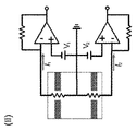
一の態様において、図2は、別の実施形態の装置の外観を示す。図2において,この装置は、スペーサーによって接続される2つの平行な膜からなるマイクロ流体チップ(「2核チップ(dual−core chip)」と称される)を含む。各膜は、この膜の中心を通る単一ビームによって穿孔された細孔(図示せず)を含む。更に、この装置はこのチップのためのテフロン(登録商標)ハウジングを好ましくは有する。このハウジングはチャンバA〜Cの密封された分離状態を確実にし、電解質のための抵抗への最小限のアクセスを提供し、各電圧が各細孔に主に印加されることを確実にする。 In one aspect, FIG. 2 shows the appearance of another embodiment device. In FIG. 2, the device includes a microfluidic chip (referred to as a “dual-core chip”) consisting of two parallel membranes connected by a spacer. Each membrane includes pores (not shown) drilled by a single beam through the center of the membrane. Furthermore, the device preferably has a Teflon housing for the chip. This housing ensures a sealed isolation of chambers A-C, provides minimal access to resistance for the electrolyte, and ensures that each voltage is applied primarily to each pore.
より具体的には、細孔を有する膜は、厚さ5〜100nmのケイ素、窒化ケイ素,または二酸化ケイ素ウィンドウを備えるTEM(透過電子顕微鏡法)グリッドで作られることができる。スペーサーはこの膜を分離するために使用されることができ、これは、絶縁体(SU−8,フォトレジスト,PECVD酸化物,ALD酸化物,ALDアルミナ)または蒸着金属(Ag,Au,Pt)材料を用い、かつ、これらの膜間のチャンバBの他の含水部分内の小さい体積を占領することによってなされる。ホルダーは、チャンバBの最も大きい体積部分を備える水性槽に着座される。チャンバAおよびCは、(低アクセス抵抗のための)膜シールに導くより大きなチャネルによってアクセス可能である。 More specifically, the membrane with pores can be made of a TEM (Transmission Electron Microscopy) grid with a 5-100 nm thick silicon, silicon nitride or silicon dioxide window. Spacers can be used to separate this film, which can be an insulator (SU-8, photoresist, PECVD oxide, ALD oxide, ALD alumina) or vapor deposited metal (Ag, Au, Pt). This is done by using materials and occupying a small volume in the other hydrous part of chamber B between these membranes. The holder is seated in an aqueous bath with the largest volume of chamber B. Chambers A and C are accessible by larger channels leading to a membrane seal (for low access resistance).
集中された電子またはイオンビームは膜を通して細孔を穿孔し、それらを自然に整合させるために使用されることができる。これらの細孔は正確なビーム焦点を各層に印加することによってより小さなサイズに形成(縮小)することもできる。任意の単体のナノ細孔穿孔方法は2つの膜内に1対の細孔を穿孔するために使用されることもでき、所定の方法にとって可能な穿孔深さおよび膜の厚さを考慮に入れる。膜厚を更に洗練するために、マイクロ細孔を所定の深さに予備穿孔し、膜の残りを貫通するナノ細孔を作ることも可能である。 A focused electron or ion beam can be used to drill pores through the membrane and align them naturally. These pores can also be formed (reduced) to a smaller size by applying a precise beam focus to each layer. Any single nanopore drilling method can also be used to drill a pair of pores in two membranes, taking into account the possible drilling depth and membrane thickness for a given method . To further refine the film thickness, it is also possible to pre-drill micropores to a predetermined depth to create nanopores that penetrate the rest of the film.
別の態様において、ハイブリッド細孔を形成するために個体のナノ細孔内に生体ナノ細孔を挿入することを、2細孔方法において片方のナノ細孔または両方のナノ細孔において用いることができる(ホール他、Nat. Nanotech., 5(12):874−7,2010)。生体細孔はイオン電流測定の感度を増し、一本鎖ポリヌクレオチドが(例えばシークエンシングのために)2細孔装置(デバイス)において捕捉され制御されるべき場合に有用である。 In another aspect, inserting bio-nanopores within individual nanopores to form hybrid pores can be used in one or both nanopores in a two-pore method. (Hall et al., Nat. Nanotech., 5 (12): 874-7, 2010). Biopores increase the sensitivity of ionic current measurements and are useful when single-stranded polynucleotides are to be captured and controlled in a two-pore device (device) (eg, for sequencing).
2細孔装置での分子の動きの制御
この装置の細孔に存在する電圧により、荷電された分子をチャンバ間の細孔を通して移動することができる。移動の速度および方向は、電圧の強度および方向によって制御することができる。更に、2つの電圧のそれぞれを独立して調節することができるため、荷電された分子の移動および速度を各チャンバにおいて細かく制御することができる。
Controlling the movement of molecules in a two-pore device The voltage present in the pores of this device allows charged molecules to move through the pores between the chambers. The speed and direction of movement can be controlled by the strength and direction of the voltage. Furthermore, since each of the two voltages can be adjusted independently, the movement and speed of the charged molecules can be finely controlled in each chamber.
例えば、この装置は、制御された状態で2つの正に荷電された分子を混ぜるために使用されることができる。このために,第1の分子が上部チャンバに最初に装填され、第2の分子が下部チャンバに装填される。第1のポートにおける第1の電圧は、上部チャンバから中間チャンバ内に第1の分子の移動を誘発する。同様に、第1の電圧の方向とは反対の方向への第2の電圧は,下部チャンバから中間チャンバ内への第2の分子の移動を誘発することができる。電圧が反対方向であることによって、両方の分子が互いに反応するように中間チャンバ内に保持される。更に、電圧の相対強度を調節することによって、各分子の流入速度が微調整され、制御反応に導く。 For example, the device can be used to mix two positively charged molecules in a controlled manner. For this purpose, a first molecule is first loaded into the upper chamber and a second molecule is loaded into the lower chamber. The first voltage at the first port induces movement of the first molecule from the upper chamber into the intermediate chamber. Similarly, a second voltage in a direction opposite to the direction of the first voltage can induce movement of the second molecule from the lower chamber into the intermediate chamber. By having the voltage in the opposite direction, both molecules are held in the intermediate chamber so that they react with each other. Furthermore, by adjusting the relative strength of the voltage, the inflow rate of each molecule is finely adjusted, leading to a control reaction.
別の例は、両方の細孔の深さにこれら2つの細孔間の距離を加算して組み合わせた距離よりも長い長さを有する荷電ポリマー(例えばポリヌクレオチド)に関する。例えば、1000bp(塩基対)dsDNA(二本鎖DNA)は、長さ340nmであり、20nmだけ離れた長さ10nmの2つの細孔によって及ぶ40nmよりも実質的に長い。第1のステップにおいて,ポリヌクレオチドは上部チャンバまたは下部チャンバのいずれかに装填される。生理的条件(〜pH7.4)の下でその負電荷によって、電圧が印加された細孔をまたいでポリヌクレオチドを移動することができる。従って、第2のステップにおいて、同じ方向および同じもしくは類似する強度の2つの電圧が細孔に印加され、両方の細孔に亘るポリヌクレオチドの移動を順に誘発する。 Another example relates to charged polymers (eg, polynucleotides) having a length that is longer than the combined distance of the depth of both pores plus the distance between these two pores. For example, 1000 bp (base pair) dsDNA (double stranded DNA) is 340 nm in length and is substantially longer than 40 nm spanned by two 10 nm long pores separated by 20 nm. In the first step, the polynucleotide is loaded into either the upper chamber or the lower chamber. Due to its negative charge under physiological conditions (˜pH 7.4), the polynucleotide can be moved across the pores to which the voltage is applied. Thus, in the second step, two voltages of the same direction and of the same or similar strength are applied to the pores, in order to induce polynucleotide movement across both pores.
ポリヌクレオチドが第2の細孔に到達する頃、これらの電圧のうち一または両方を変化することができる。このポリヌクレオチドは両方の細孔をカバーする距離よりも長いため、このポリヌクレオチドが第2の細孔に到達するときには第1の細孔内にもある。従って、第1の細孔での電圧の方向の急速な変化は、ポリヌクレオチドを引っ張り第2の細孔から離す力を生成する(図1(III))。 One or both of these voltages can be changed when the polynucleotide reaches the second pore. Since this polynucleotide is longer than the distance covering both pores, it is also in the first pore when it reaches the second pore. Thus, a rapid change in the direction of the voltage in the first pore generates a force that pulls the polynucleotide away from the second pore (FIG. 1 (III)).
この時点で、第1の細孔での電圧誘起による力が第2の細孔での電圧誘起による力よりも小さい場合、このポリヌクレオチドは第2の細孔に向かって両方の細孔にまたがることを続けるが、より低速にである。これに関し、ポリヌクレオチドの移動の速度および方向は両方の電圧の方向および強度によって制御されることができる。更に後述するように、係る移動の微調整は幅広い用途を有すると理解されたい。 At this point, if the voltage induced force in the first pore is less than the voltage induced force in the second pore, the polynucleotide will span both pores toward the second pore. Keep going, but slower. In this regard, the speed and direction of movement of the polynucleotide can be controlled by the direction and intensity of both voltages. As will be further described below, it should be understood that such fine adjustment of movement has a wide range of applications.
従って、一の態様において、細孔を通しての荷電ポリマーの移動を制御する方法が提供される。この方法は(a)上記実施形態のいずれかの上部チャンバ,中間チャンバまたは下部チャンバのうち一つにおいて荷電ポリマーを備えるサンプルを装填するステップを備え、ここで、この装置は上部チャンバと中間チャンバとの間の第1の電圧、および中間チャンバと部チャンバとの間の第2の電圧を供給するための電源に接続され、(b)ポリマーがチャンバ間を移動するように初期の第1の電圧および初期の第2の電圧を設定するステップを備え、これにより第1のおよび第2の細孔に亘ってポリマーを所在させ、(c)両方の電圧がこの荷電されたポリマーを引っ張り、中間チャンバから離す力を生成するように(電圧−競合モード),第1の電圧および第2の電圧を調節するステップを備え、ここで、荷電ポリマーがいずれかの方向および制御された状態にて両方の細孔に亘って移動するようにこれら2つの電圧は制御状態の下、異なる強度である。 Thus, in one aspect, a method for controlling the movement of a charged polymer through a pore is provided. The method comprises (a) loading a sample comprising a charged polymer in one of the upper chamber, middle chamber or lower chamber of any of the above embodiments, wherein the apparatus comprises an upper chamber, an intermediate chamber, Connected to a power source for supplying a first voltage between the first chamber and a second voltage between the intermediate chamber and the second chamber, and (b) an initial first voltage so that the polymer moves between the chambers. And setting an initial second voltage, thereby locating the polymer across the first and second pores, (c) both voltages pulling the charged polymer, and the intermediate chamber Adjusting the first voltage and the second voltage to generate a force away from (voltage-competitive mode), wherein the charged polymer is in either direction These two voltages so as to move across both pores in the preliminary control state under the control conditions are different intensities.
ステップ(c)における電圧−競合モードを設定する目的のために、各細孔における各電圧によって生じる相対力は、使用される各2細孔装置のために決定されるべきであり、これはキャリブレーション実験を伴うことで、ポリヌクレオチドの動きに対する異なる電圧値の影響を観察することによってなされる(移動はポリヌクレオチドにおける位置が分かった検出可能(detectable)な特徴を検知(sensing)することによって測定されることができ、係る特徴の例は後述する)。力が各共通の電圧に等しい場合、例えば、(接地された中間チャンバに比して上部および下部チャンバ内の共通する極性を備える)各細孔での同じ電圧値を使用することで、熱運動なしにゼロ・ネット移動が生じる(ブラウン運動の存在および影響は後述する)。この力が各共通電圧にて等しくない場合、等しい力を達成することは、共通の電圧にてより小さい力を受ける細孔でのより大きな電圧の特定および使用を必要とする。電圧−競合モードのためのキャリブレーションが各2細孔装置のために必要とされ、かつ特定の荷電ポリマーまたは分子(各細孔を通る特徴が力に影響するもの)のために必要とされる。 For the purpose of setting the voltage-competition mode in step (c), the relative force produced by each voltage in each pore should be determined for each two-pore device used, which is In conjunction with the experiment, the effect of different voltage values on the movement of the polynucleotide is observed (movement is measured by sensing a detectable feature whose position in the polynucleotide is known. Examples of such features are described below). If the force is equal to each common voltage, for example, using the same voltage value at each pore (with a common polarity in the upper and lower chambers compared to the grounded middle chamber), the thermal motion Without zero net movement (the existence and impact of Brownian motion will be discussed later). If this force is not equal at each common voltage, achieving equal force requires the identification and use of a larger voltage at the pores that receive less force at the common voltage. Calibration for voltage-competitive mode is required for each two-pore device and for a specific charged polymer or molecule (the feature through each pore affects the force) .
一の態様において、サンプル(試料)が上部チャンバ内に装填され、初期の第1の電圧が荷電ポリマーを上部チャンバから中間チャンバに引っ張るように設定され、初期の第2の電圧はポリマーを中間チャンバから下部チャンバに引っ張るように設定される。同様に、サンプルは最初に下部チャンバ内に装填されることができる。 In one embodiment, a sample is loaded into the upper chamber, the initial first voltage is set to pull the charged polymer from the upper chamber to the intermediate chamber, and the initial second voltage is set to pull the polymer to the intermediate chamber. To pull to the lower chamber. Similarly, the sample can be initially loaded into the lower chamber.
別の態様において、サンプルは中間チャンバ内に装填され、最初の第1の電圧は荷電ポリマーを中間チャンバから上部チャンバに引っ張るように設定され、最初の第2の電圧は荷電ポリマーを中間チャンバから下部チャンバに引っ張るように設定される。 In another aspect, the sample is loaded into the intermediate chamber, the first first voltage is set to pull the charged polymer from the intermediate chamber to the upper chamber, and the first second voltage is charged from the intermediate chamber to the lower chamber. Set to pull into chamber.
いくつかの態様において、荷電ポリマーはポリヌクレオチドまたはポリペプチドである。特定の態様において、荷電ポリマーはポリヌクレオチドである。非限定的なポリヌクレオチドの例は、二本鎖DNA,一本鎖DNA,二本鎖RNA,一本鎖RNA,およびDNA−RNAハイブリッドを含む。 In some embodiments, the charged polymer is a polynucleotide or polypeptide. In certain embodiments, the charged polymer is a polynucleotide. Non-limiting examples of polynucleotides include double stranded DNA, single stranded DNA, double stranded RNA, single stranded RNA, and DNA-RNA hybrids.
一の態様において、ステップ(c)にて調節された第1の電圧および第2の電圧は、これら2つの電圧間の差と同程度に強度が高い約10倍〜約10,000倍である。例えば、これらの2つの電圧はそれぞれ90mVおよび100mVである。電圧の強度(〜100mV)はそれら(10mV)の間の差の約10倍である。いくつかの態様において、電圧の強度はそれらの間の差と同程度に高く少なくとも約15倍,20倍,25倍,30倍,35倍,40倍,50倍,100倍,150倍,200倍,250倍,300倍,400倍,500倍,1000倍,2000倍,3000倍,4000倍,5000倍,6000倍,7000倍,8000倍または9000倍である。いくつかの態様において、電圧の強度は、電圧の強度はそれらの間の差と同程度に約10000倍,9000倍,8000倍,7000倍,6000倍,5000倍,4000倍,3000倍,2000倍,1000倍,500倍,400倍,300倍,200倍,または100倍以下である。 In one aspect, the first voltage and the second voltage adjusted in step (c) are about 10 times to about 10,000 times as strong as the difference between the two voltages. . For example, these two voltages are 90 mV and 100 mV, respectively. The intensity of the voltage (˜100 mV) is about 10 times the difference between them (10 mV). In some embodiments, the strength of the voltage is as high as the difference between them, at least about 15, 20, 25, 30, 35, 40, 50, 100, 150, 200 They are double, 250 times, 300 times, 400 times, 500 times, 1000 times, 2000 times, 3000 times, 4000 times, 5000 times, 6000 times, 7000 times, 8000 times or 9000 times. In some embodiments, the strength of the voltage is about 10,000 times, 9000 times, 8000 times, 7000 times, 6000 times, 5000 times, 4000 times, 3000 times, 2000 times that of the voltage is as much as the difference between them. It is less than 1000 times, 1000 times, 500 times, 400 times, 300 times, 200 times, or 100 times.
一の態様において、ステップ(c)にて第1の電圧および第2の電圧のリアルタイム調節またはオンライン調節が行われ、これは、専用ハードウェアおよびソフトウェアを用いて数百メガヘルツまでのクロックレートにてアクティブ制御またはフィードバック制御によって行われる。第1の電圧もしくは第2の電圧または両方の電圧の自動化された制御は第1のイオン電流もしくは第2のイオン電流または両方のイオン電流測定のフィードバックに基づく。
2細孔装置を使用した分子の分析
In one aspect, a real time or online adjustment of the first voltage and the second voltage is made in step (c), using dedicated hardware and software at clock rates up to several hundred megahertz. Performed by active control or feedback control. Automated control of the first voltage or the second voltage or both voltages is based on feedback of the first or second ion current or both ion current measurements.
Molecular analysis using a two-pore device
本願の2細孔装置は、細孔に印加された制御電圧によってこの装置内を動くかこの装置内に保持される分子または粒子の分析を行うために用いられることができる。一の態様において、この分析は細孔のいずれかまたは両方にて行われる。各電圧クランプまたはパッチクランプシステムは各細孔を通るイオン電流を測定し、この測定された電流は、通過する荷電された粒子または分子の存在を検出するのに使用され、または通過する荷電された粒子または分子に関連する特徴を検出するのに使用される。 The two-pore device of the present application can be used to analyze molecules or particles that move through or are held in the device by a control voltage applied to the pores. In one embodiment, this analysis is performed on either or both of the pores. Each voltage clamp or patch clamp system measures the ionic current through each pore, and this measured current is used to detect the presence of charged particles or molecules passing through or charged through. Used to detect features associated with particles or molecules.
上記の様に、ポリヌクレオチドは同じ方向を有する2つの電圧によって両方の細孔内に装填されることができる。この例において、一旦、第1の細孔に印加された電圧の方向が反転され、新たな電圧誘起による力の強度が第2の細孔に印加された電圧誘起による力よりも僅かに小さくなると、ポリヌクレオチドは同じ方向への移動を継続するが、著しく低い速度にてである。これに関し、第2の細孔に電圧を供給する増幅器も第2の細孔を通過する電流を測定し、次にイオン電流は、各異なるヌクレオチドの通過が(例えば、イオン電流振幅における移行に基づく)異なる電流界シグナチャーを引き起こすため、細孔を通過するヌクレオチドの特定をする。従って、ポリヌクレオチドにおける各ヌクレオチドの特定はポリヌクレオチドのシークエンスを明らかにする。 As described above, a polynucleotide can be loaded into both pores by two voltages having the same direction. In this example, once the direction of the voltage applied to the first pore is reversed, the strength of the new voltage-induced force is slightly smaller than the voltage-induced force applied to the second pore. The polynucleotide continues to move in the same direction, but at a significantly lower rate. In this regard, an amplifier that supplies a voltage to the second pore also measures the current passing through the second pore, and then the ionic current is determined by the passage of each different nucleotide (eg, based on a transition in ionic current amplitude). ) Identify the nucleotides that pass through the pores to trigger different current field signatures. Thus, the identification of each nucleotide in the polynucleotide reveals the sequence of the polynucleotide.
いくつかの態様において、ポリヌクレオチドを再シークエンシングするための繰り返しのコントロールド・デリバリーはシークエンシングの質を更に改善する。各電圧は、各方向においてコントロールド・デリバリーのためにより大きくなりながら極性が反転される。更に、2つの細孔を通る2つの電流が、正確性の改善に関係づけられると考えられる。ブラウン運動は分子の動きに変動を与えることができ、分子のコントロールド・デリバリーに影響を与えることが考えられる。しかしながら、係る影響は、例えば、DNAシークエンシング中に、DNAの繰り返しのコントロールド・デリバリーによって、およびシークエンシング測定値を平均化することによって最小限にするか、または避けることができる。更に、巨大分子(例えばポリヌクレオチドおよびポリペプチド)の制御された動きへのブラウン運動のインパクトは、特に競合力が巨大分子を引っぱりこの分子内に張力を生成するときには取るに足らないと考えられる。 In some embodiments, repeated controlled delivery for resequencing a polynucleotide further improves the quality of the sequencing. Each voltage while seeking polarity Do large due for Controlled Delivery in each direction is reversed. Furthermore, it is believed that the two currents through the two pores are related to improved accuracy . Brownian motion is given example can Rukoto a change in the movement of molecules, it is considered that affect the control de delivery of the molecule. However, such effects can be minimized or avoided , for example, by repeated controlled delivery of DNA during DNA sequencing and by averaging sequencing measurements. Furthermore, the impact of the Brownian motion of the controlled movement of the macromolecules (e.g. polynucleotides and polypeptides), consider a trivial when the particular competitive generates tension in the molecule pull macromolecules It is done.
係る方法は、先行技術において解決されていない問題への解決策を提供する。 Such a method provides a solution to problems not solved in the prior art.
例えば、ナノ細孔シークエンシングに必要なコントロールド・デリバリーおよび正確な検知を達成するためには2つの矛盾する障害があることが知られている。一方は、十分なシークエンシング感度を提供するために細孔にて比較的高電圧が必要とされることである。他方において,高電圧によってポリヌクレオチドが細孔を速く通過することになり、各ヌクレオチドの特定のために十分な時間がなくなる。 For example, it is known that there are two conflicting failure to achieve the controlled-delivery and accurate detection required nanopore sequencing. One is that a relatively high voltage is required at the pores to provide sufficient sequencing sensitivity. On the other hand, the high voltage will cause the polynucleotide to rapidly pass through the pore, leaving no time for identification of each nucleotide.
より具体的には、ナノ細孔シークエンシングのプラットフォームは、細孔を通過するポリヌクレオチドの速度が1ms/ヌクレオチド(nt)またはそれ以下に制御されることを要求する一方、なおシークエンス感応性電流を生成することを要求する。このことは電流シグナチャーを検出するために十分な高信号対雑音(高電圧がよい)を必要とするが、測定値が確実に記録帯域幅内にあるようにするために細孔を通る分子の動きが十分に遅いこと(低電圧がよい)を必要とする。単一細孔の態様において、ポリヌクレオチド速度は、電圧に比例し、よって電圧が高いほど、検知のために良いが、ポリヌクレオチド速度を低下させるためにはより悪くなる:速度はポリヌクレオチド捕捉を促進する電圧にて1μs/ntおよびこれより速い(>1000倍は速すぎる)。一方、電圧が低くなると検知性能を減じ、読み出しの正確性を害するブラウン運動によって引き起こされる速度変動の相対的な寄与度も増す。 More specifically, the nanopore sequencing platform, while the speed of the polynucleotide through a pore requests Rukoto is controlled to 1 ms / nucleotides (nt) or less, still a sequence sensitive current Request to generate. Although this requires a sufficiently high signal-to-noise (high voltage good) to detect the current signature over, molecules through the pores to the measured value to be within reliably record bandwidth movement requires a sufficiently slow (low voltage good). In a single pore embodiment, the polynucleotide rate is proportional to the voltage, so the higher the voltage, the better for detection, but worse for decreasing the polynucleotide rate: the rate is greater for polynucleotide capture. 1 μs / nt and faster at accelerating voltages (> 1000 times too fast). On the other hand , lowering the voltage reduces the detection performance and also increases the relative contribution of speed fluctuations caused by Brownian motion, which impairs read accuracy.
これらの障害に対処する方法のうち、特化したナノ細孔技術においてのみ作用する酵素または光学機器の使用を伴わない方法は、本明細書に記載したもの以外に現在存在しない。 Of the methods that address these obstacles, there are currently no methods other than those described herein that do not involve the use of enzymes or optical instruments that only work in specialized nanopore technology.
いくつかのアプローチが検出能力の欠如および低電圧に関する問題に対処するために提案されている。一つは、生体ナノ細孔の感度を向上させるためにこれらの生体ナノ細孔を作りかえることである。別のものは、グラフェン膜を使用するものであり、これは、単一シートとしてssDNA(単鎖DNA)においてヌクレオチド間の距離よりも薄い。更に別のものは、ナノ細孔に近接して測定された補助電流の使用である(例えば、トンネル電流)。 Several approaches have been proposed to address the problems with lack of detection capability and low voltage. One is to recreate these biological nanopores in order to improve the sensitivity of the biological nanopores. Another is to use a graphene film, which is thinner than the distance between nucleotides in ssDNA (single-stranded DNA) as a single sheet. Yet another is the use of an auxiliary current measured in proximity to the nanopore (eg, tunneling current).
生体ナノ細孔は、第1のアプローチにおいてテストされた。α溶血素ナノ細孔は、研究において最も一般に使用される生体細孔である。研究結果は、α溶血素が、ホモポリマー内の単一ヌクレオチド置換を解像し、あるいはさもなければ全てが核酸塩基であるDNAのなかの脱塩基(1’,2’−ジデオキシ)残基を解像可能であることを示した。しかしながら、単一ヌクレオチド感度は、(イオン電流がチャネルにおいて〜10ヌクレオチドによって影響を受ける)野生形(WT)α溶血素を用いた異種DNAにおいては可能ではない。α溶血素のタンパク質工学はDNA分析およびシークエンシングに対するその感度を向上させるために使用されている。係る突然変異の細孔の1つは、4つのヌクレオシド5’−一リン酸塩分子を高精度で識別することができる、共有結合された分子アダプター(クラーク他、Nat. Nanotech, 4(4):265−70,2009)を備えるα溶血素を使用する。しかしながら、この突然変異の細孔は、細孔を通過する完全な異種ssDNAをシークエンシングするための感度を有しないと思われる。 Biological nanopores were tested in the first approach. Alpha hemolysin nanopores are the most commonly used biological pores in research. Findings, alpha hemolysin, abasic of among resolved single nucleotide substitution within homopolymers, or otherwise all of the DNA is a nucleic acid base (1 ', 2'-dideoxy) residues It was shown that it can be resolved . However, single nucleotide sensitivity (ion current is influenced by the 10 nucleotides in the channel) is not possible in a heterologous DNA with wild-type (WT) alpha-hemolysin. Protein engineering of α-hemolysin is used to improve the sensitivity to DNA analysis and sequencing. Engaging Ru One of the pores of the mutation can be identified four nucleoside 5'-phosphate molecular accurately, covalently bound molecular adapter (Clark other, Nat. Nanotech, 4 ( 4): α-hemolysin with 265-70, 2009) is used. However, this mutant pore does not appear to have the sensitivity to sequence the complete heterologous ssDNA passing through the pore.
別の例示的な生体細孔はMspAであり、これは、イオン電流の感度をチャネルの底に集中させる漏斗状の形状を有する。更に、MspAおよびα溶血素を通過するDNAの速度の減少は、酵素を用いることによって達成することができる。(マンラノ他、Nature Biotechnology,30:349−53,2012)の図1に示されるように、DNAの速度の減少はMspAナノ細孔上に位置する酵素によって達成される。しかしながら、このことは、非決定性の検知期間、引き返しによって引き起こされる繰り返しの読み出し、およびホモポリマー領域を検出することができないといった結果となる。phi29(ファイ29)ポリメラーゼ媒介性DNA変位の機構は、α溶血素について(チャーフ他、 Nat.Biotech., 30(4):344−8,2012)で開発され、より感度の高いMspAナノ細孔(マンラオ他、Nature Biotechnology,30:349−53,2012)上で実施された。重合触媒された変位の段階的速度は2.5〜40nt/sであり、DNA速度低下のための要件に合う。しかしながら、生体細孔上の酵素が変位の速度を低下させることができる一方、各ヌクレオチドの滞留時間の制御を欠き、このことは繰り返しのブラインドトラッキングを非常に困難なものにするだろうし、単一ヌクレオチド読み出しの長い中止時間と区別することを困難にするだろう。感度に関し,(Manrao他、Nature Biotechnology,30:349−53,2012)の図3に示されるように、繰り返しのDNAテンプレートを読み出すことは、MspA上のファイ29によって達成することができる。図(3a)は、繰り返しのCATトリヌクレオチドからなるDNAテンプレートに対する追跡例を示し、このシークエンスの中間には1つのCAGトリプレットという例外がある。*は、2つのレベル間の繰り返しの遷移(これは酵素に基づく制御方法に本来備わっており、読み出しエラーを引き起こす)として(人の分析によって)検出された「トグル(toggles)」を表す。図(3b)は(3a)の理想化も示し、公知のDNAシークエンスと合致するレベルの平均電流を備え、(3a)に示された測定された期間の差異を除く。理想化は、単一dG置換によって妨害された3つのレベルの繰り返しパターンを示す。4つのレベルは、置換の最も近くで最も大きな偏差を備えるように単一dGによって影響され、これは残留電流が〜4ヌクレオチド程度で主に影響を受けることを示唆している。MspAを流れるイオン電流が開口に最も近接する〜4ヌクレオチドによる影響をうけることは、シークエンスを特定するのに相当な複雑性を加える。当該技術において示唆されるように44=256の組み合わせのそれぞれをマッピングする明確な電流振幅のライブラリを作ることが理想的であるが、係るライブラリは実現が困難である。その理由は、チャネル電流の記録における特定ステップの遷移は、片振幅法を伴う少なくとも2の信号対雑音比(SNR)を必要とするからである(マルコフに基づく方法ではSNR≧1.5)。記録帯域幅にて0.5pAのRMS雑音を伴うと、振幅シフトは必要とされるSNRを有するために少なくとも1pAでなければならず、MspAを用いて40pAの振幅レンジ内で〜40段の検出可能レベルのみ(またはSNR1.5にて最大でも53段のレベル)という結果になる。更に、このレンジは一様には利用されないだろうから、観察されるレベルは40段より少なくなり、更なるフィルタリングが雑音を減少して振幅弁別を加えることができるけれども、それは既に存在するより速いssDNA運動遷移をより多く失うという結果にもなる。 Another exemplary biopore is MspA, which has a funnel shape that concentrates the sensitivity of the ionic current to the bottom of the channel. Furthermore, a decrease in the rate of DNA passing through MspA and α-hemolysin can be achieved by using enzymes. As shown in FIG. 1 of (Manlano et al., Nature Biotechnology, 30: 349-53, 2012), a decrease in the rate of DNA is achieved by enzymes located on MspA nanopores. However, this results in a non-deterministic sensing period, repeated readout caused by pullback, and inability to detect the homopolymer region. phi29 mechanism (phi 29) polymerase mediated DNA displacement, the α-hemolysin (Chafu other, Nat.Biotech, 30 (4): . 344-8,2012) developed by, more sensitive MspA nanopore (Manrao other, Nature Biotechnology, 30: 349-53,2012) was performed on. The step rate of polymerization catalyzed displacement is 2.5-40 nt / s, meeting the requirements for DNA rate reduction. However, while enzymes on biological pores can reduce the rate of displacement , they lack control over the residence time of each nucleotide, which would make repeated blind tracking very difficult and single It will be difficult to distinguish from long stoppage times for nucleotide reads. With regard to sensitivity, reading the repetitive DNA template can be accomplished by Phi 29 on MspA, as shown in FIG. 3 (Manrao et al., Nature Biotechnology, 30: 349-53, 2012). Figure (3a) shows a tracking example for a DNA template consisting of repetitive CAT trinucleotides, with the exception of one CAG triplet in the middle of this sequence. * Repeats transitions between two levels (which is inherent in the control method based on the enzyme, causing read errors) as (by human analysis) representative of the detected "toggle (toggles)". Figure (3b) also shows the idealization of (3a), with a level of average current consistent with the known DNA sequence, and excluding the measured time difference shown in (3a). The idealization shows a three level repeating pattern that is disturbed by a single dG substitution. The four levels are affected by a single dG with the largest deviation closest to the substitution, suggesting that the residual current is mainly affected by ~ 4 nucleotides. The ionic current flowing through MspA is affected by the ~ 4 nucleotides closest to the opening, adding considerable complexity to specifying the sequence. While it is ideal to create a library of distinct current amplitudes that maps each of the 4 4 = 256 combinations as suggested in the art, such a library is difficult to implement. The reason is that a specific step transition in the recording of the channel current requires a signal-to-noise ratio (SNR) of at least 2 with a single amplitude method (SNR ≧ 1.5 for Markov based methods). When accompanied by RMS noise of 0.5pA by the recording bandwidth must be at least 1pA to have a SNR that is amplitude shift required, the detection of the 40 stages in the amplitude range of the 40pA with MspA As a result, only possible levels (or 53 levels at maximum at SNR 1.5) are obtained. Furthermore, since this range will not be used uniformly, the observed level will be less than 40 stages , and although further filtering can reduce noise and add amplitude discrimination, it is faster than already exists. It also results in losing more ssDNA movement transitions.
現在、核酸シークエンシングに対してイオン電流検出が単一ヌクレオチド感度を提供することができるナノ細孔はない。依然として、生体細孔および固体の細孔(グラフェン)の感度の改善は活発であり、継続中の研究分野である。問題の一つは、イオン電流検出が、ホモポリマー領域(塩基反復)の進行を直接的に追跡できないことである。なぜなら、細孔を通ってホモポリマーssDNAが移動する際のヌクレオチド毎の信号が区別できないからである。反復を追跡することは必要不可欠である。というのも例えば、ヒトミトコンドリアDNA内の特定のモノヌクレオチド反復(7,9nt)の削除および挿入がいくつかの種類の癌に関与しているからである(サンチェス−セスペデス,他、 Cancer Research, 61(19):7015−7019,2001)。生体細孔上の酵素は、変位の速度を低下させることができる一方、各ヌクレオチドの滞留時間の制御を欠く。他方では、2細孔制御による一定の送出速度を用いることで、偶発的な中断がなくなり、リピート長さ(反復長)の正確な推定をなしうる。何度もリピートセクションを再読み出しすることで推定誤りも向上し、誤り限界をも特定することができ、このことは酵素によってもたらされる重合化学を逆行させる必要なくなされうる。 Currently, there are no nanopores where ion current detection can provide single nucleotide sensitivity for nucleic acid sequencing. Still, the improvement in sensitivity of biopores and solid pores (graphene) remains an active and ongoing research area. One problem is that ionic current detection cannot directly track the progress of the homopolymer region (base repeats). This is because the signal for each nucleotide when the homopolymer ssDNA moves through the pore cannot be distinguished. It is essential to keep track of iterations. This is because, for example, deletion and insertion of specific mononucleotide repeats (7,9 nt) in human mitochondrial DNA are involved in several types of cancer (Sanchez-Cespedes, et al., Cancer Research, 61 (19): 7015-7019, 2001). While enzymes on biological pores can reduce the rate of displacement , they lack control over the residence time of each nucleotide. On the other hand, by using a constant delivery speed by two-pore control, there is no accidental interruption, and an accurate estimation of the repeat length (repetition length) can be made. Rereading the repeat section over and over again improves the estimation error and can also identify error limits, which can be done without having to reverse the polymerization chemistry provided by the enzyme.
最近の研究が示したことは、単一ナノ細孔では、速度の低下は単に電圧の低下のみによっては実現することができないということである(ルー他、 Biophysical Journal,101(1):70−9,2011)。代わりに、電圧が減少されると、一本鎖DNA(ssDNA)の速度はよりランダムになる(引き返しを含む)。なぜなら、ブラウン運動の速度変動への寄与が大きくなるからである。研究はまた、ブラウン運動によって引き起こされる速度変動(この速度変動はさもなければシークエンシング測定を失敗させる)を抑制するために高電圧力が必要とされることも示し、これは理想化された単一ヌクレオチド感応性ナノ細孔センサーを用いた場合でさえもである。 Recent studies have shown that in single nanopores, a decrease in velocity cannot be achieved simply by a decrease in voltage (Lu et al., Biophysical Journal, 101 (1): 70- 9, 2011). Alternatively, when the voltage is reduced, the speed of the single-stranded DNA (ssDNA) is ing more random (including turn-back). This is because the contribution to the speed fluctuation of the Brownian motion becomes large. The study also is Ru speed fluctuation caused by the Brownian motion (this speed change is otherwise sequencing fail the measurement) are shown also to be a high voltage power necessary for suppressing, which was idealized Even when using single nucleotide sensitive nanopore sensors.
本願において提供される、2細孔装置に基づくこのシークエンシング方法は、これらの問題への解決策を提供し、既存の方法に対する付加的な利点を提供する。シークエンシングのために十分な感度を有する1つまたは2つの細孔と連携して、高電圧または低電圧におけるこの2細孔制御は、単一ナノ細孔態様のシークエンシング速度制御の問題を解決する。係る細孔には固体の基板に内蔵された生体細孔、固体の基板全体に形成された膜における生体細孔、または固体の細孔(例えば、グラフェン,ケイ素,または他の基板において)が含まれる。一の態様において、MspAといった生体細孔上のファイ29といった酵素を一または両方の細孔にて使用することができ、これには、シークエンシングのための大信号を生成するのに使用される高電圧、および、各細孔上の適所に酵素を保持し重合触媒されたDNA移動を可能にするのに十分な、各酵素に力を生成する作動電圧(但しその酵素を失速させるか解離させるほど大きくはない)を伴う。係る構成は、測定信号を著しく増大させ、2細孔が同時にDNAの1ストランドを読み出すことを可能にすることによって、チャーフ他(Nat. Biotech.,30(4):344−8,2012およびマンラオ他、Nature Biotechnology,30:349−53,2012)における方法を改善することができる。 This sequencing method based on the two-pore device provided in this application provides a solution to these problems and provides additional advantages over existing methods. In conjunction with one or two pores having sufficient sensitivity for sequencing, definitive this 2 pore control the high or low voltage, the sequencing speed control of a single nanopore aspect problem Solve. Biological pores incorporated in the substrate of the solid in the pores, the biological pores in film formed on the entire substrate of a solid or solid pore (e.g., graphene, silicon or the other substrate), is free of Ru rare. In one embodiment, the enzyme such as phi 29 on biological pores such MspA can be used in one or both of the pores, the this is used to generate a large signal for sequencing A high voltage and an operating voltage that produces a force on each enzyme that is sufficient to hold the enzyme in place on each pore and allow polymerization-catalyzed DNA movement (but to stall or dissociate that enzyme) Not as large). Configuration of significantly increase the measurement signal by 2 pore to allow the simultaneous reading one scan tiger command of DNA, Chafu other (Nat Biotech, 30 (4) :.. 344-8,2012 And Manlao et al., Nature Biotechnology, 30: 349-53, 2012).
更に、本願に開示された方法は、イオン電流検出を用いた細孔における検出感度を保証するために十分高い電圧を細孔にて生成することができる。高電圧は、各細孔を一定速度で通過することを保証するのに十分なほど、ブラウン運動を抑制し、各細孔の外側のDNAの構成がどちらかの方向へのDNAの移動のエネルギー特性に影響すると考えられる。更に、この方法(図1(III))において用いられる電圧競合は、分子が分析に十分な時間を細孔にて過ごすように調節されることができる。更に、本方法は、酵素,光学部品,またはDNAのアタッチメントの必要性がない。従って、この方法は、分子送出速度を規制しつつ、ナノ細孔を通る高SN比の検出電流を提供し、これは単一ナノ細孔態様では不可能な能力である。 Furthermore, the method disclosed herein can generate a sufficiently high voltage at the pores in order to ensure detection sensitivity definitive in pores with ion current detection. High voltage, enough to ensure that through each pore at a fixed rate, to suppress the Brownian motion, the movement of the DNA in the direction configuration either outside the DNA of each pore It is thought to affect the energy characteristics. Furthermore, the voltage competition used in this method (FIG. 1 (III)) can be adjusted so that the molecule spends sufficient time in the pore for analysis . Furthermore, the method does not require the attachment of enzymes, optical components, or DNA. Therefore, this method, while regulating the molecular delivery rates, providing a sensing current of a high SN ratio Ru through the nanopore, which is the ability not possible with a single nanopore manner.
この方法は荷電ポリマーにおけるモノマーの組成を特定するのに使用されることができる。一の態様において、モノマー単位はポリマーが単一鎖のDNAまたはRNAである場合にヌクレオチドである。別の態様において、モノマーユニットはポリマーが二重鎖である場合にヌクレオチド対であり得る。 This method can be used to identify the composition of monomers in a charged polymer. In one embodiment, the monomer unit is a nucleotide when the polymer is single stranded DNA or RNA. In another embodiment, the monomer unit may be a nucleotide pair when the polymer is double stranded.
一の態様において、この方法は、特に結合した分子が荷電される場合に、ポリマーへの修飾(例えばモノマーへの分子結合)を特定するのに使用されることができる。結合分子は電荷されなくてもよいが、中性分子はそのサイズによってイオン電流を変化させることができる。 In one embodiment, this method can be used to identify modifications to a polymer (eg, molecular attachment to a monomer), particularly when the attached molecule is charged. The binding molecule may not be charged, but the neutral molecule can change the ionic current depending on its size.
別の態様において、この修飾はポリマーに対する分子の結合を含む。例えば、DNA分子のために、結合分子はDNA結合タンパク(例えばRecA,NF−κΒおよびp53)であり得る。更に別の態様において、この修飾は特定のモノマーまたはフラグメントに結合する粒子である。例えば、遺伝子型決定またはDNAマッピングの目的のために特定のDNA箇所に結合された量子ドットまたは蛍光標識がこの装置によって検出されることができる。従って、本願に開示された装置は、遺伝子型決定およびDNAマッピングの廉価な方法も提供する(これらに限定されない)。 In another embodiment, the modification involves the attachment of a molecule to the polymer. For example, for a DNA molecule, the binding molecule can be a DNA binding protein (eg, RecA, NF-κΒ and p53). In yet another embodiment, the modification is a particle that binds to a particular monomer or fragment. For example, quantum dots or fluorescent labels attached to specific DNA sites for genotyping or DNA mapping purposes can be detected by this device. Thus, the devices disclosed herein also provide (but are not limited to) inexpensive methods of genotyping and DNA mapping.
一の態様において、ポリマーがその一端部でビード(bead)といった固体支持体に接合される。 In one embodiment, the polymer is bonded at one end to a solid support such as a bead.
一実施形態において、ポリヌクレオチドのシークエンスを決定する方法を提供し、この方法は、(a)上記実施形態のいずれかの装置の上部チャンバにおいてポリヌクレオチドを含むサンプルを装填するステップを含み、ここで、この装置は上部チャンバと中間チャンバとの間の第1の電圧と、中間チャンバと下部チャンバとの間の第2の電圧とを提供する電源に接続され、このポリヌクレオチドはポリヌクレオチドの一端で固体支持体に任意に接合され、(b)ポリヌクレオチドが上部チャンバから中間チャンバおよび中間チャンバから下部チャンバに移動するように、初期の第1の電圧および初期の第2の電圧を設定するステップを備え、これにより、前記第1の細孔および第2の細孔の両方に亘って前記ポリマーを配置し、(c)両方の電圧が前記荷電ポリマーを前記中間チャンバから引き離すための力を生成するように第1の電圧および第2の電圧を調節するステップを備え、前記ポリヌクレオチドが一方向にかつ制御された方法で両方の細孔に亘って移動するように前記2つの電圧は制御された条件下で強度が異なり、(d)前記ヌクレオチドが細孔を通過するときに前記細孔のうちいずれかのイオン電流を測定することによって、当該細孔を通過するポリヌクレオチドの各ヌクレオチドを特定するステップを備える。
実施例
In one embodiment, a method for determining a sequence of a polynucleotide is provided, the method comprising: (a) loading a sample comprising the polynucleotide in the upper chamber of the apparatus of any of the above embodiments, wherein The device is connected to a power source providing a first voltage between the upper chamber and the middle chamber and a second voltage between the middle chamber and the lower chamber, the polynucleotide at one end of the polynucleotide. Optionally joining to a solid support; (b) setting an initial first voltage and an initial second voltage such that the polynucleotide moves from the upper chamber to the intermediate chamber and from the intermediate chamber to the lower chamber; Comprises placing the polymer across both the first and second pores, and (c) both Adjusting a first voltage and a second voltage such that a voltage generates a force to pull the charged polymer away from the intermediate chamber, wherein the polynucleotide is both in a unidirectional and controlled manner. The two voltages have different intensities under controlled conditions to move across the pore, and (d) measure the ionic current of one of the pores as the nucleotide passes through the pore. In particular, the method includes the step of identifying each nucleotide of the polynucleotide that passes through the pore.
Example
本技術は、以下の実施例を参照して更に定義される。糸および方法に対する多くの変更が本発明の範囲を逸脱せずに行われ得ることは当業者には明らかであろう。 The technology is further defined with reference to the following examples. It will be apparent to those skilled in the art that many modifications to the yarn and method can be made without departing from the scope of the invention.
実施例1.細孔内の個別のdsDNA分子の捕捉および制御
この実施例は、2細孔装置において各細孔内へのDNAの捕捉が、測定された各独立したイオン細孔電流の変化として容易に検出されることを示す。
Example 1. Capture and control of individual dsDNA molecules within the pore This example shows that in a two-pore device, the capture of DNA into each pore is easily detected as a change in each measured independent ionic pore current. Indicates that
この実施例は、一端に接着されたビードを伴うdsDNAおよびこれを伴わないdsDNAを用いてデュアル細孔捕捉を実証する。ビードに連結されたssDNAを用いた実験も詳しく探り得る。 This example demonstrates dual pore capture using dsDNA with and without a bead attached to one end. Experiments with linked ssDNA to beads also Ru detail explore obtained.
DNAの捕捉および失速の際、ビードに最も近い細孔電圧(V1,図1(I)(チャンバAからの捕捉の場合))は、当該DNAに働く競合力がこれをチャンバAに向かって引き戻すまで反転され、増大されうる。いずれかの細孔のイオン電流は、実験の間、当該DNAの捕捉および退出を容易に検出しうる。 During acquisition and stall of DNA, nearest the pore voltage to the bead (V1, when the acquisition of Figures 1 (I) (chamber A)) is pulled back competing forces acting on the DNA is this toward the chamber A to be reversed, Ru cormorant is increased. Ion current in one of the pores during the experiment, Ru easily detected Siu capture and exit of the DNA.
ビードが使用される際、このビードは細孔のいずれかまたは両方を通過することができない適切なサイズを有する。ビード対DNAが1対1であることを確実にする方法は、当該技術分野にて開発されてきた。例えば、ビオチン化DNA重複部位(またはssDNA)に共役する一価のストレプトアビジン被覆された量子ドット(QDs;QD655,インビトロゲン)は、直径が20〜30nmのビードを提供することができ、金粒子またはラテックスを使用することによってより大きなビード(30〜100nm)も可能である。流体力学および荷電へのビードの影響は、これが捕捉速度に関係することから、実験を設計する際に検討され得る。 When a bead is used, the bead has an appropriate size that cannot pass through either or both of the pores. Methods to ensure that bead-to-DNA is 1: 1 have been developed in the art. For example, monovalent streptavidin-coated quantum dots (QDs; QD655, Invitrogen) conjugated to biotinylated DNA overlap sites (or ssDNA) can provide beads with diameters of 20-30 nm, and gold particles or more large beads (30 to 100 nm) is also possible by using latex. The effect of the bead on hydrodynamics and charge can be considered when designing the experiment since this is related to the capture rate.
ビードなしでは、dsDNAは〜0.1ms/kbpにて細孔を通過する。長さ500bpおよび4kbpのDNA,およびλファージdsDNA分子(〜48kbp)が使用される。DNAサンプルは、チャンバAからの捕捉とチャンバBを通じたチャンバCへの通過とを促進するために各細孔に対して共通の電圧極性を用いてチャンバAから両方の細孔内に配送されうる(図1(I))。dsDNAの持続長が長ければ(1クーン(Kuhn)長は100nm)、各細孔内部のDNAセグメントがおそらく完全に伸びて棒状になることが確実になる。電圧およびイオン濃度は適切な捕捉速度を特定するために変えることができる。様々な緩衝されたイオン濃度が、捕捉速度と、各細孔においてDNAの存在を示すコンダクタンスシフト値とを高めるか変化させるために各チャンバにおいて使用されうる。
Without the bead, dsDNA passes through the pores at ˜0.1 ms / kbp. 500 bp and 4 kbp DNA in length and λ phage dsDNA molecules (˜48 kbp) are used. DNA samples will be delivered from the chamber A by using a common voltage polarity for each pore to facilitate the passage to the chamber C through the acquisition and chamber B from chamber A to both pores (FIG. 1 (I)). The longer the persistence length of dsDNA (1 Kuhn (Kuhn)
直径が10nm以上のナノ細孔を用いることで、dsDNAとナノ細孔壁との間の干渉(例えば、摩擦および固着)は最小限になる。細孔が大きくなると、dsDNAが、折り畳まれた構造および折り畳まれていない構造で捕捉されうるが、一列縦列の(折り畳まれていない)構造は、より高電圧かつより短い(≦3kbp)dsDNAにてより生じ易い。500nm以下の細孔内の距離に対して、(チャンバAとBとの間にある)第1の細孔での捕捉に引き続いてデュアル細孔捕捉が起きる可能性は、1M KCl中、200mV以上の電圧において非常に高い。 By diameter using nanopores least 10 nm, interference between the dsDNA and the nano pore walls (e.g., friction and sticking) is ing to a minimum. When the pore is increased, in-dsDNA, but may be captured in a folded structure and unfolded structure, a row column (unfolded) structure is less than the higher voltage and (≦ 3 kbp) dsDNA More likely to occur. With respect to the distance 500nm within the following pores, (located between the chambers A and B) possibly dual pore capture occurs subsequent to the acquisition of the first pores in 1M KC l, 200 mV very high in the above voltage.
電圧の影響が熱拡散より優位でかつ高い確率で捕捉をもたらす半径距離は、一定の細孔サイズ範囲(直径6〜15nm)、電圧(120〜500mV)に対して、少なくとも4kbpの長さのdsDNAについて、少なくとも900nm(細孔内の距離よりも大きい)であると推定されている(ガーショーおよびゴロブチェンコ, Nature Nanotechnology,2:775−779,2007)。これらの発見は、dsDNAの単一(第1の)細孔捕捉に引き続いて、高い確率でdsDNAの迅速なデュアル細孔捕捉があることを裏付ける。 Radial distance the influence of the voltage results in capture by the superiority and high probability than the thermal diffusion constant pore size range (diameter 6~15Nm), for the voltage (120~500MV), at least 4kbp length of dsDNA for, it is estimated that at least 900 nm (greater than the distance in the pores) (Gasho and Gorobuchenko, Nature Nanotechnology, 2: 775-779,2007) . These findings confirm that there is a high probability of rapid dual pore capture of dsDNA following a single (first) pore capture of dsDNA.
2細孔によるDNAの捕捉および制御は、アクティブ制御ハードウェアおよび実時間アルゴリズムから利益を得ることができる。発明者らは、DNA制御のためのアクティブ制御ハードウェア/ソフトウェアを開発した。例えば、ギアーファス,Biophys.J.,100:1509−16,2011);ウィルソン他、ACS Nano.,3(4):995−1003,2009;およびベンナー他、Nat. Nanotech.,2(11):718−24,2007を参照。有用なソフトウェアはFPGA(フィールド・プログラマブル・ゲート・アレイ)システム(PCI−7831R,National Instruments))において実装されたLabVIEWソフトウェア(Version 8,National Instruments,Austin,TX)である。参照したFPGAは4つの増幅器まで同時に制御することができる。更に、PC上でデータをデジタル化して記録(ログ)するために使用されるAxon Digidata1440Aデータ収集システム(Data Acquisition System)は、並列の8つの増幅器までの電圧および電流を記録するのに十分な16個の入力チャネルを有する。実時間制御および測定のためのハードウェア/ソフトウェアに合う他の実時間オペレーティングシステムは、増幅器を制御し、データをデジタル化して記録するために使用されることもできる。 DNA capture and control by two pores can benefit from active control hardware and real-time algorithms. The inventors have developed active control hardware / software for DNA control. See, for example, Gearface, Biophys. J. et al. , 100: 1509-16, 2011); Wilson et al., ACS Nano. , 3 (4): 995-1003, 2009; and Benner et al., Nat. Nanotech. , 2 (11): 718-24, 2007. A useful software is LabVIEW software (Version 8, National Instruments, Austin, TX) implemented in an FPGA (Field Programmable Gate Array) system (PCI-7831R, National Instruments). The referenced FPGA can control up to four amplifiers simultaneously. Furthermore, the Axon Digidata 1440A data acquisition system (Data Acquisition System) used to digitize and log data on a PC is sufficient to record the voltage and current up to eight amplifiers in parallel. Has input channels. Other real-time operating systems that fit hardware / software for real-time control and measurement can also be used to control the amplifier and digitize and record the data.
発明者らは、省スペースおよびマルチチャネル装置における一または複数のナノ細孔の使用を機能化および最適化するために、「ナノクランプ」と称する低雑音電圧クランプ増幅器(キム他、IEEE Trans. On Biom.Circ.And Syst.In press,May 2012;キム他、Elec.Lette.,47(15):844−6,July,2011;およびキム他、Proceedings of the IEEE International SoC Design Conference (ISOCC),November,2010)も開発した。任意の他の商業的卓上電圧クランプまたはパッチクランプ増幅器,または一体型電圧クランプまたはパッチクランプ増幅器は、2つの細孔制御および測定のために使用されることができる。 The inventors have developed a low noise voltage clamp amplifier called “Nano Clamp” (Kim et al., IEEE Trans. On) to functionalize and optimize the use of one or more nanopores in space saving and multi-channel devices. Biom.Circ.And Syst.In press, May 2012; Kim et al., Elec.Lette., 47 (15): 844-6, July, 2011; and Kim et al., Proceedings of the IEEE International SoC Design (CCC). November, 2010) was also developed. Any other commercial desktop voltage clamp or patch clamp amplifier, or integrated voltage clamp or patch clamp amplifier can be used for the two pore controls and measurements.
様々な固体細孔材料および直径に対し、0.1〜10kbpが変位するのに〜1msかかる。FPGAで制御された増幅器によって、0.020ms(ミリ秒)以内に捕捉を検出し競合電圧制御を開始することができ、これは1kbp DNAの合計通過速度1msよりもかなり速く、よって、(ビードアタッチメントを有しない)DNAが逃げる前に制御方法を動作させる可能性も高い。制御の実証として、分子が細孔から退出するまでの時間および退出方向を、競合電圧間の強度および差異の関数として実証することができる(図1(III))。単一の細孔実験において、長い(≧1kbp)dsDNAが細孔を通る速度は、大きく変動することが実験的に観察され、これらの変動は拡散ブラウン運動に帰するには大きすぎる。(ルー他,Biophysical Journal,101(1):70−79,2011)において、正味速度変動(すなわち、合計通過時間で除したDNA長さ)の主要源は、誘引する電圧領域が延びている、細孔に入ったDNAの部分に加えて、細孔にまだ入っていないDNAのうち、電圧に影響を受ける部分によって誘発される粘性抵抗によるものとしてモデリングされた。このモデルは実験データと妥当に適合した。注目すべきは、dsDNAの質量中心が捕捉の際に細孔と同一線上にある場合、正味速度は速くなるが、もし細孔の中心から外れた場合には、正味速度は遅くなる。競合電圧が2細孔装置内で使用されるとき、dsDNA速度は、電圧差が十分に高くないのであれば、この粘性抵抗によってもたらされる摂動によって影響を受けない。この理由は、細孔および競合電圧の両方によるdsDNA捕捉がなされた後に、細孔間のdsDNAは完全に延びて棒状となっており、したがっていずれの細孔入口付近でも構造体を作ることに関与できないからである。一方、細孔の外側上のdsDNA構造体は各局所細孔電圧によって常に中間チャネルから離れるように強制されることから、細孔入口動力学を複雑化する可能性はより低い。斯かる構造体は、コントロールド・デリバリー動力学に影響を与えることができ、動力学への影響を定量化するためにキャリブレーション実験を使用することができる。
For various solid pore materials and diameters, it takes ˜1 ms to displace 0.1-10 kbp. By a controlled amplifier in FPGA, it is possible to start detecting conflict voltage control capture within 0.020Ms (milliseconds), which is much faster than the total passing speed of
ランダムな横方向のDNA運動によってもたらされる力の不確実性はおそらく最小限である。更に、電圧力は、DNA運動の逆方向に電気浸透流(EOF)を起こし、対イオン流がない場合よりも低速でDNAを移動させる。分子の半径位置が様々に異なることで、ナノ細孔に様々なEOFフィールドを生じることから、問題の一つは、実効電荷密度そして正味駆動力が、速度変動をもたらすDNA半径位置の変動の間に十分変化するかどうかである。1M KClにおけるDNAの実効電荷密度は細孔壁とDNAとの間の1nm以上の距離に対して安定していると考えられる。 Uncertainty force exerted by the DNA motion random lateral is probably minimal. Moreover, the voltage power, electroosmotic flow in the direction opposite to the DNA movement cause (EOF), if there is no counter ion flow low speed to move the DNA than. The radial position of the molecule is different for different, since it results in a variety of EOF field nanopores, is one problem, the effective charge density and a net driving force, while the variation of the DNA radial position results in speed variations Whether it changes enough. The effective charge density of DNA in 1M KC l is considered to be stable with respect to 1nm or more of the distance between the pore walls and DNA.
更に、SiNナノ細孔は、本来DNAを排除する負の表面電荷を有する。それゆえに、分子は半径位置変動を受けるけれども、数ナノメートルよりも大きい直径を備えるSiN細孔を用いることによって、各一定電圧値が2細孔のそれぞれにて一定の実効的な力をもたらし易く、したがって2細孔設定において2つの競合電圧を使用するときにより大きな力の方向において一定速度をもたらし易い。他の細孔材料表面を処理することにより、SiNに匹敵する効果を生じ得る。 Furthermore, SiN nanopores have a negative surface charge that essentially excludes DNA. Therefore, although the molecules are subject to radial position variations, by using SiN pores with a diameter greater than a few nanometers, each constant voltage value is likely to yield a constant effective force in each of the two pores. Thus, when using two competing voltages in a two-pore setting, it is likely to provide a constant speed in the direction of larger forces. By treating other porous material surfaces , effects comparable to SiN can be produced .
ブラウン運動によってもたらされるランダムなDNAの並進運動によって引き起こされる速度の不確実性は、競合電圧を高めることによって減少し得る。そのような減少が起こるか否かを決定するために、実験が行われうる。単一ナノ細孔の研究は(ルー他、Biophysical Journal,101(1):70−79,2011)競合力を高めることでブラウン運動によって生じる不確実性を減少することができることを裏付ける。研究は、ブラウン運動(速い(ナノセカンド)タイムスケールにおいて生じる)によってもたらされる速度変動およびかかる変動に起因するシークエンシングエラーを分析した。仮想的かつ理想化された単一ヌクレオチドセンサー(>22MHz帯域幅にてノイズフリーの検出)を前提とすると、ブラウン運動だけで75%読み出しエラーになる。エラーを予測するための関連パラメータは、k B T/F*(0.34nm)と表され、熱エネルギーとDNAを変位するためになされる仕事との比率であり、その距離はヌクレオチド間の距離a(0.34nm)である。この比率において力F=Vλは電荷密度λ(dsDNAについて0.2e−/bp)を備えるDNAを駆動する電圧Vである。当該制御方法については、電圧を50倍に高めることで5%読み出しエラーになり、より高電圧は更にエラーを改善する。しかしながら、単一細孔について、平均速度ν(−)(注:νの上にハイフン。以下同じ)は、拡散定数をdとしてF*d/(k B T)と表されることから、DNA速度もFにつれて高まり、シークエンシング帯域幅により非現実的な要求をする。 Uncertainty rate caused by translational movement of the random DNA caused by Brownian motion may be reduced by increasing the contention voltage. To determine whether such reduction occurs, Ru cormorants is performed experiments. Studies single nanopore (router, Biophysical Journal, 101 (1) : 70-79,2011) Ru confirmed that by increasing the competitiveness can reduce uncertainty caused by Brownian motion. The study analyzed the speed fluctuations caused by Brownian motion, which occurs on the fast (nanosecond) time scale, and sequencing errors due to such fluctuations . Assuming a virtual and idealized single nucleotide sensor (noise-free detection at> 22 MHz bandwidth), only Brownian motion results in a 75% read error. Related parameters for predicting the error is expressed as k B T / F * (0.34nm ), is the ratio of the work done to displace the thermal energy and DNA, the distance between the distance nucleotides a (0.34 nm). Force F = Vlambda in this ratio is the charge density lambda (for dsDNA 0.2e - / bp) is a voltage V for driving the DNA comprising a. For this control method, Ri Do 5% reading error by increasing the voltage to 50 times, to improve the higher voltage is further errors. However, for a single pore, the average velocity ν (-) (Note:. Hyphen same on the [nu), since it is expressed as F * d / a diffusion constant as d (k B T), DNA The speed also increases with F , making unrealistic demands on the sequencing bandwidth.
22MHz帯域幅を維持するために、単一ナノ細孔についての力が50倍に増加すると、同じν(−)を維持するために溶液粘度を50倍に増加しならなければならないであろう。しかしながら、実際には、22MHz帯域幅は、単一ヌクレオチドシークエンシングについて任意の実験的ナノ細孔プラットフォームが実証したか実証することを約束するレベルよりも既にはるかに高い。更に、粘度を増加させることによっては、単一ナノ細孔で10倍までしかDNAを遅くすることができない(フォロゲア,他、Nano Lett.,5(9):1734−7,2005)。2細孔プラットフォームを用いれば、各電圧を十分に高く維持することができ、これによりブラウン運動によって生じる変動を抑制することができ、一方、正味DNA速度を決定する差動電圧は、制御速度が確実に実際のシークエンシング帯域幅(名目上1kHz)以内となるように調節されうる。ブラウン運動によってもたらされる速度変動を抑制する別の方法は、帰還制御を用いることである。一の態様において、10kHz帯域幅での第1の細孔電圧の作動に10kHz帯域幅の第2の細孔電流をフィードバックすると、ブラウン運動は、DNAにある検出可能な特徴をこれらのkHz閉ループ帯域幅で第2の細孔内およびこの付近に留めるように制御するよう相殺され得る。この能力は、Hz閉ループ帯域幅における分子に取り付けられたビードの光学的強制により、2つの空間次元および仕事においてブラウン運動を抑制した反ブラウン動電学的(ABEL)トラップの一次元アナログである(ワングおよびモエナー,ACS Nano,5:5792−9,2011)。 To maintain the 22MHz bandwidth, result increased 50 times the force for a single nanopore, the same [nu (-) would have become the solution viscosity increased 50-fold to maintain. In practice, however, the 22 MHz bandwidth is already much higher than the level that any experimental nanopore platform has demonstrated or promises to demonstrate for single nucleotide sequencing. Furthermore, by increasing the viscosity, it is not possible to slow down the DNA only up to 10 times in a single nanopore (Forogea other, Nano Lett, 5 (9) :. 1734-7,2005). Lever with 2 pore platform, the voltages can be kept sufficiently high, This ensures it is possible to suppress fluctuations arising by Brownian motion, whereas the differential voltage to determine the net DNA rate, control rate Ru adjusted Sareu to ensure that the less actual sequencing bandwidth (nominally 1 kHz). Another method for suppressing speed fluctuation Ru caused by Brownian motion is the use of feedback control. In one embodiment, when feeding back the second pore current 10kHz bandwidth to the operation of the first pores voltage at 10kHz bandwidth, Brownian motion, these kHz closed loop band detectable features in DNA The width can be offset to control to remain in and near the second pore . This ability, by optical forcing the bead attached to the molecule in Hz closed-loop bandwidth, which is one-dimensional analog of the two spatial dimensions and counterclockwise Brown electrokinetic (ABEL) inhibited Brownian motion in the work trap ( Wang and Moener, ACS Nano, 5: 5792-9, 2011).
実施例2. DNAに結合したRecAフィラメントの検出および局所化
この実施例は、2細孔装置が特知惠のシークエンスを有するかこれに結合しないタンパク質のために、dsDNAへのDNA結合タンパクの結合をマッピングするために使用することができることを示す。
Example 2 Detection and Localization of RecA Filaments Bound to DNA This example is to map the binding of DNA binding proteins to dsDNA for proteins for which the two-pore device has a known sequence or does not bind to it. Indicates that it can be used.
実施例1において実証されるように、DNAサンプルはチャンバAから捕捉することができる。RecAタンパクは、壊れたDNAを損傷を受けていないDNAの相補領域とペアにするATP依存DNA鎖交換反応を触媒する。不十分に加水分解するATP類似体ATPγSを用いて、dsDNAに結合されたRecAフィラメントは、第1に生理食塩水内で組み立てられる際に高い塩において非常に安定している(例えば、1M KCl)。ゆっくり加水分解されるATPγSに対する代替として、この実施例はADP−AlF4(四フッ化アルミニウム)も使用することができ、これは全く入れ替わることがなく、RecAをより強固にDNAに結合させる。 As demonstrated in Example 1, a DNA sample can be captured from chamber A. RecA protein catalyzes an ATP-dependent DNA strand exchange reaction that pairs broken DNA with the complementary region of undamaged DNA. Poorly using hydrolyzes ATP analogs ATPyS, RecA filaments coupled to dsDNA is very stable at high salt when assembled in saline first (e.g., 1M KC l ). As an alternative to ATPγS is slowly hydrolyzed, this embodiment ADP-A l F4 (aluminum tetrafluoride) may also be used, which without completely interchanged, Ru to bind the RecA more firmly DNA .
20〜30nmナノ細孔を通してλ−DNAに結合されたRecAフィラメントの検出は、実証されているが(コワルクジク他、Nano Lett.,10(1):324−8,2010;スミーツ他、Nano Lett.9(9):3089−95,2009;およびホール他、Nano Lett.9(12):4441−5,2009)、長さ<20bpのフィラメント(6個以下のRecAタンパク)は、単一ナノ細孔を用いても、変位速度と測定SNRとの間の結合によって解決することができない。 Although the detection of RecA filaments bound to λ-DNA through 20-30 nm nanopores has been demonstrated (Kowakujik et al., Nano Lett., 10 (1): 324-8, 2010; Sumets et al., Nano Lett. 9 (9): 3089-95, 2009; and Hall et al., Nano Lett. 9 (12): 4441-5, 2009), filaments <20 bp in length (less than 6 RecA proteins) The use of holes cannot be solved by the coupling between the displacement rate and the measured SNR.
この実施例の初期実験は、ほぼ被覆されていない、部分的に被覆されている、および完全に被覆されているDNAを生成するために、RecAの変化する濃度にされているビード結合および非結合λ−DNAを用いる。各細孔電流の実時間監視は、コントロールド・デリバリーの進歩状況を計るために使用することができ、フィラメントの位置マッピングのために相関される。各DNAの繰り返し測定はRecAマッピングの正確性を向上させる。 Initial experiments in this example show that bead binding and non-binding at varying concentrations of RecA to produce DNA that is nearly uncoated, partially coated, and fully coated. λ-DNA is used. Real-time monitoring of each pore current can be used to measure the progress of controlled delivery and is correlated for filament position mapping. Repeated measurement of each DNA improves the accuracy of RecA mapping.
RecAがDNAに結合されるときに、加えられた電荷およびバルク、ならびに高濃度の塩における安定性は、提案された器具を伴うコントロールド・デリバリーの間に検出および位置マッピングを試みるために理想的な候補となる。 When RecA is bound to DNA, the added charge and bulk, and stability in high concentrations of salt, is ideal for attempting detection and location mapping during controlled delivery with the proposed instrument. A good candidate.
更に、RecA結合されたDNAの制御は、変位を止めるためにビードを取り付けることなく試みることができる。実施例1のdsDNA実験と同様に、能動的電圧制御は、DNAがナノ細孔を出る前に競合電圧制御を迅速に開始するために使用することができる。AsDNAに結合する荷電された種(species)がDNAの正味荷電および剛性を変えることによって電場におけるDNAの機動性に影響するため、移動制御調整実験は、dsDNAの移動を制御するために使用される力平衡への、dsDNAに結合するRecAの影響を試験することができる。 Furthermore, control of RecA-bound DNA can be attempted without attaching a bead to stop displacement . Similar to the dsDNA experiment of Example 1, active voltage control can be used to quickly initiate competitive voltage control before the DNA exits the nanopore. Migration control coordination experiments are used to control the movement of dsDNA because charged species that bind to AsDNA affect the mobility of the DNA in the electric field by altering the net charge and stiffness of the DNA. The effect of RecA binding to dsDNA on force balance can be tested.
この実施例は、低いRecA濃度で観察された最も短いフィラメント長さを高いSNRかつ十分に遅い制御された速度にて測定することができ、分離して結合された任意のRecAタンパクが存在しているかを検出することができる。 This example can measure the shortest filament length observed at low RecA concentrations with high SNR and a sufficiently slow controlled rate, and there is any RecA protein bound separately. It can be detected.
従って、2細孔装置は基本的な調査のために全く新しい単一分子の器具を提供し、なぜなら付加的なタンパクがRecA−DNAフィラメントに結合するのを検出する能力を試験することができるからであり、このことはフィラメント幅を広くし、よって観察された電流の減少によって検出される。例えば、RecA−DNAフィラメントに結合するタンパクは、LexAおよびバクテリアフォージラムダリプレッサーを含み、これらは細胞の状態を検出して下流の調節事象をオンまたはオフに切り替えるためにRecAを使用する。 Thus, the two-pore device provides an entirely new single molecule instrument for basic investigations because it can test the ability to detect additional protein binding to RecA-DNA filaments. This is detected by increasing the filament width and thus the observed decrease in current. For example, proteins that bind to RecA-DNA filaments include LexA and a bacterial forge lambda repressor, which use RecA to detect cellular status and turn downstream regulatory events on or off.
キャリブレーション実験はDNAの特定のシークエンス(位置)に結合するタンパクを検出することを含み、タンパクによってもたらされた電流シフトが細孔を通してDNAの速度および速度制御性能の推定を可能にする。dsDNAの特定の箇所に結合する例示的なタンパクは、Lacリプレッサー(21bpセグメントに結合する)、ラムダファージ・リプレッサー(λ−DNAの複数のオペレーター部位を有する),および他のタンパクを含む。 Calibration experiments involve detecting proteins that bind to specific sequences (positions) of DNA, and the current shift introduced by the proteins allows estimation of DNA velocity and rate control performance through the pores. Exemplary proteins that bind to specific sites in dsDNA include the Lac repressor (which binds to the 21 bp segment), the lambda phage repressor (which has multiple lambda-DNA operator sites), and other proteins.
実施例3.一本鎖DNA内の二本鎖セグメントの検出および局所化
この実施例は、可変長の二本鎖セグメントを備える10kbまでのssDNAの生成を実証する。
Example 3 Detection and localization of double stranded segments within single stranded DNA This example demonstrates the generation of up to 10 kb of ssDNA with variable length double stranded segments.
第1のステップにおいて、10kbpのdsDNAはロングレンジPCRによって作ることができる。鎖の一端はビードアタッチメントのためのビオチン化であり、この鎖は化学変性によって分離される。その後、ビードのない10kb ssDNAは2細孔実験において測定された鎖として機能する。所望のサイズを備える相補的一本鎖セグメントは、PCRによって作られ、ビード捕捉および鎖状分離(strand separation)が続く。 In the first step, 10 kbp dsDNA can be made by long range PCR. One end of the chain is biotinylated for bead attachment and this chain is separated by chemical denaturation. The 10 kb ssDNA without beads then functions as the strand measured in the two-pore experiment. Complementary single stranded segments with the desired size are made by PCR followed by bead capture and strand separation.
測定された10kb ssDNA内の複数の箇所にて可変長のssDNAセグメントを使用することができ、1セットの100ntセグメントで始まる。単一固体細孔を通るイオン電流は、dsDNAをssDNAホモポリマーならびにプリンおよびピリミジンホモポリマーから識別するために使用された(スキナー他、Nano Lett.,9(8):2953−60,Jan 2009)。よって、DNAの単一鎖セグメントを二本鎖セグメントから識別する可能性は2細孔装置を用いて十分な高電圧にて高いものとなる。ssDNAセグメント対dsDNAセグメントをマッピングすることで、ハイブリダイゼーションでアシストされた方法(hybridization−assisted process)(提案されたこの方法は高価なハイブリダイゼーションでアシストされた処理に依存する)を用いてナノ細孔シークエンシングを可能にし、長距離において目標DNAシークエンスの位置および特定を明らかにするために使用することができる(目標とされたシークエンシング)。単一鎖DNA結合(SSB)タンパクの使用の可能性を探ることもできる(ssDNAに結合することによってイオン電流においてssDNA対dsDNAの差異を更に拡大し、dsDNAよりも大きなインピーダンスを作るビードとして)。
実施例4.長いssDNAの捕捉および制御ならびにRecAの局所化
Variable length ssDNA segments can be used at multiple locations within the measured 10 kb ssDNA, starting with a set of 100 nt segments. Ionic current through a single solid pore was used to distinguish dsDNA from ssDNA homopolymers and purine and pyrimidine homopolymers (Skinner et al., Nano Lett., 9 (8): 2953-60, Jan 2009). . Thus, the possibility of discriminating single-stranded segments of DNA from double-stranded segments is high at a sufficiently high voltage using a two-pore device. By mapping the ssDNA segment to the dsDNA segment, a nanopore using a hybridization-assisted process (the proposed method relies on expensive hybridization-assisted treatment). Allows sequencing and can be used to reveal the location and identification of target DNA sequences over long distances (targeted sequencing). The possibility of using single stranded DNA binding (SSB) proteins can also be explored (as a bead that further expands the ssDNA vs. dsDNA difference in ionic current by binding to ssDNA, creating a larger impedance than dsDNA).
Example 4 Long ssDNA capture and control and RecA localization
この実施例は長いssDNAの捕捉および制御ならびにRecAの検出および局所化を実証する。更に、この2細孔装置はssDNA内のプリン対ピリミジンホモポリマーセグメントを検出することができる。 This example demonstrates long ssDNA capture and control and RecA detection and localization. Furthermore, this two-pore device can detect purine versus pyrimidine homopolymer segments in ssDNA.
20nmのSiN膜における10nmの細孔を通しての7kbのssDNAの確率論的なもつれは、ステファン他、 Nano Lett.,10:1414−20,2010に示されるように行うことができる。ステファン他2010における単一ナノ細孔方法が、もつれたssDNAと細孔/膜表面との間の機械的接触力によってssDNAをほぐす一方、2細孔の競合電圧セットアップは、各細孔に最も近いDNA骨格への各電圧力の作用によって、ssDNAを十分に高い競合電圧にて細孔の近くかつ細孔の間でもつれを電気泳動的力的にほぐさせることができると考えられる。 Stochastic tangles of 7 kb ssDNA through 10 nm pores in 20 nm SiN films are described by Stefan et al., Nano Lett. , 10: 1414-20, 2010. The single nanopore method in Stefan et al. 2010 unravels ssDNA by mechanical contact forces between the entangled ssDNA and the pore / membrane surface, while the two-pore competitive voltage setup is closest to each pore By the action of each voltage force on the DNA backbone, it is considered that ssDNA can be electrophoretically loosened near and between the pores at a sufficiently high competitive voltage.
ほぐしおよびこれに続く2細孔セットアップによるssDNAの速度の正確な制御は、長いssDNA分子の最終的なシークエンシングのために重要である。十分に高い電圧(〜400mV)にて、ss−DNA内のプリンおよびピリミジンホモポリマーセグメントを区別することが可能であり、(スキナー他、Nano Lett.,9(8):2953−60,Jan 2009),このことは診断用途および癌の研究のために有用である。 Accurate control of the ssDNA rate by unwinding and subsequent two-pore setup is important for the final sequencing of long ssDNA molecules. With sufficiently high voltage (˜400 mV) it is possible to distinguish purine and pyrimidine homopolymer segments within ss-DNA (Skinner et al., Nano Lett., 9 (8): 2953-60, Jan 2009). ), Which is useful for diagnostic applications and cancer research.
この実施例は、ssDNAに結合してより大きなインピーダンスを作ることによってssDNAイオン電流から区別可能な検出可能な「速度−bumps」として、RecAあるいはおそらく他の一鎖およびDNA 結合(SSB) タンパクの使用の可能性も探る。これらの速度抑止物(speed bump)は、制御されたssDNA速度の直接定量化を可能にし、そして必要とされる1ms/ntが達成可能であることを実証する。RecAは特定のトリヌクレオチドシークエンス箇所に結合する必要はないが、好ましくはTGG繰り返しシークエンスに結合し、RecAフィラメントが既に形成されたところに結合する傾向もあるため、キャリブレーション実験は、特定の既知のシークエンス箇所に結合する他のssDNA結合分子の使用を必要とする。結合箇所が各細孔を通過するときに検出可能な結合箇所を知っていることは、競合電圧値の関数として分子の速度を決定するために必要である。非限定的な実施例は、一または複数の既知の箇所に融合する二重鎖(あるいはビードで拘束された二重鎖)を使用することであり、これから電流のシフトが各細孔を通して各重複部位の経路を検出するために使用することができ、そして選択された電圧値のための通過する鎖速度を推定する。続いて、RecAフィラメントが形成され、係る分子において検出され、ベンチマーク検出点として重複部位の特徴を維持し、これに関連してRecAフィラメントが検出され、それらの位置が推定される。 This example uses RecA or possibly other single strand and DNA binding (SSB) protein as a detectable “rate-bumps” that can be distinguished from ssDNA ionic currents by binding to ssDNA and creating greater impedance. Also explore the possibilities. These speed bumps allow direct quantification of the controlled ssDNA rate and demonstrate that the required 1 ms / nt is achievable. Since RecA does not need to bind to a specific trinucleotide sequence, but preferably it binds to a TGG repeat sequence and also tends to bind where the RecA filament has already formed, Requires the use of other ssDNA binding molecules that bind to the sequence site. Knowing the binding site that can be detected as the binding site passes through each pore is necessary to determine the velocity of the molecule as a function of the competitive voltage value. A non-limiting example is to use a duplex (or a bead constrained duplex) that fuses to one or more known locations, from which each current shift is duplicated through each pore. Can be used to detect the site path and estimate the passing chain velocity for the selected voltage value. Subsequently, RecA filaments are formed and detected in such molecules, maintaining the features of the overlapping sites as benchmark detection points, in association with which RecA filaments are detected and their positions are estimated.
遺伝的なハプロタイプを決定する方法および蛍光標識をdsDNA内に組み込むことによるDNAマッピングの方法(シヤオ他、米国特許第7771944号B2,2010)も、2細孔装置を使用することができ、なぜなら、ビードラベル(例えば、量子ドット,または任意の蛍光標識)はよりバルキーであり、ちょうどdsDNA上の結合タンパクがなすように電流においてシフトを生じさせるからである。更に、2細孔方法はより単純で、ラベル位置を検出してマッピングするために、高分解能撮像方法(すなわち、完全内部反射蛍光顕微鏡法)を使用するよりも非常に廉価である。コントロールド・デリバリー中のブラウン運動によって生じる速度変動は、小さな特徴を検出するためよりも大きな特徴(タンパク,重複部位セグメント,ビードアタッチメント)を検出するための害がより少ない。 Methods of determining genetic haplotypes and DNA mapping by incorporating fluorescent labels into dsDNA (Shiao et al., US Pat. No. 7,771,944 B2,2010) can also use a two-pore device, because This is because bead labels (eg, quantum dots, or any fluorescent label) are more bulky and cause a shift in current just as the binding protein on the dsDNA does. Furthermore, the two-pore method is simpler and is much cheaper than using high-resolution imaging methods (ie, total internal reflection fluorescence microscopy) to detect and map label positions. Velocity fluctuations caused by Brownian motion during controlled delivery are less harmful to detect large features (proteins, overlapping site segments, bead attachments) than to detect small features.
本発明は上記実施形態とともに記載したが、上記記載および例は本発明を説明するためのものであり本発明の範囲を限定するものではないと理解されよう。本発明の範囲内の他の態様、利点および変更は当業者には自明であろう。
Although the present invention has been described with the above embodiment, it will be understood that the above description and examples are intended to illustrate the present invention and not to limit the scope of the invention. Other embodiments, advantages and modifications within the scope of the invention will be apparent to those skilled in the art.
Claims (25)
前記上部チャンバは第1の細孔を通して前記中間チャンバと連通し、前記中間チャンバは第2の細孔を通して前記下部チャンバと連通し、
前記第1の細孔および第2の細孔は各々が独立して深さを有し、直径約1nm〜約100nmであり、
前記チャンバのそれぞれは、電源に接続するための電極を備え、前記電源は、前記上部チャンバと前記中間チャンバとの間に第1の電圧と、前記中間チャンバと前記下部チャンバとの間に第2の電圧と、を提供するように構成され、前記第1の電圧または前記第2の電圧は独立して調節可能であり、
前記第1の細孔および前記第2の細孔の両方に亘って荷電ポリマーを配置したのち、前記第1の細孔および前記第2の細孔に競合電圧を印加するための前記第1の電圧または前記第2の電圧を調節する専用ハードウェアおよびソフトウェアを備えた装置。 An apparatus comprising an upper chamber, an intermediate chamber and a lower chamber,
The upper chamber communicates with the middle chamber through a first pore; the middle chamber communicates with the lower chamber through a second pore;
Each of the first and second pores independently has a depth and has a diameter of about 1 nm to about 100 nm;
Each of the chambers includes an electrode for connection to a power source, the power source having a first voltage between the upper chamber and the intermediate chamber and a second voltage between the intermediate chamber and the lower chamber. And wherein the first voltage or the second voltage is independently adjustable;
After placing a charged polymer across both the first pore and the second pore, the first for applying a competitive voltage to the first pore and the second pore A device with dedicated hardware and software for adjusting the voltage or the second voltage.
前記上部チャンバは、第1の細孔を通して前記中間チャンバと連通し、前記中間チャンバは第2の細孔を通して前記下部チャンバと連通し、前記第1の細孔および第2の細孔は各々が独立して深さを有し、直径約1nm〜約100nmであり、
前記細孔のそれぞれに電圧を印加して前記細孔のそれぞれを通るイオン電流を測定するために電圧クランプまたはパッチクランプシステムに接続するための、前記チャンバのそれぞれにある電極であって、前記中間チャンバ内の前記電極は前記2つの電圧クランプまたはパッチクランプシステムの共通するアースに接続されている電極と、
前記第1の細孔および前記第2の細孔の両方に亘って荷電ポリマーを配置したのち、前記第1の細孔および前記第2の細孔に競合電圧を印加するための前記第1の電圧または前記第2の電圧を調節する専用ハードウェアおよびソフトウェアとを備えた、装置。 An apparatus comprising an upper chamber, an intermediate chamber and a lower chamber,
The upper chamber communicates with the middle chamber through a first pore, the middle chamber communicates with the lower chamber through a second pore, and the first pore and the second pore are each Independently having a depth of about 1 nm to about 100 nm in diameter;
An electrode in each of said chambers for applying a voltage to each of said pores and connecting to a voltage clamp or patch clamp system to measure ion current through each of said pores, said intermediate The electrode in the chamber is connected to a common ground of the two voltage clamp or patch clamp systems;
After placing a charged polymer across both the first pore and the second pore, the first for applying a competitive voltage to the first pore and the second pore A device comprising dedicated hardware and software for adjusting a voltage or said second voltage.
(a)荷電ポリマーを含むサンプルを請求項10に記載の装置の前記上部チャンバ、中間チャンバまたは下部チャンバの一つに装填するステップを備え、
(b)前記ポリマーが前記チャンバ間を移動するように初期の第1の電圧および初期の第2の電圧を設定するステップを備え、これにより、前記第1の細孔および第2の細孔の両方に亘って前記ポリマーを配置し、
(c)前記第1の電圧および前記第2の電圧の両方が前記荷電ポリマーを前記中間チャンバから引き離すための力を生成するように前記第1の電圧または前記第2の電圧を調節するステップを備え、ここで、前記荷電ポリマーが一方向にかつ制御された方法で両方の細孔を横切って移動するように前記2つの電圧は制御された条件下で強度が異なる、方法。 A method for controlling the movement of a charged polymer through a pore, comprising:
Loading a sample comprising a charged polymer into one of the upper, middle or lower chambers of the apparatus of claim 10;
(B) setting an initial first voltage and an initial second voltage such that the polymer moves between the chambers, whereby the first pore and the second pore Placing the polymer across both,
(C) adjusting the first voltage or the second voltage such that both the first voltage and the second voltage generate a force to pull the charged polymer away from the intermediate chamber; Wherein the two voltages have different intensities under controlled conditions such that the charged polymer moves across both pores in one direction and in a controlled manner.
(a) ポリヌクレオチドを含むサンプルを請求項10に記載の前記装置の前記上部チャンバ内に装填するステップを備え、前記ポリヌクレオチドは当該ポリヌクレオチドの一端にて固体支持体に任意に接着され、
(b) 前記ポリヌクレオチドが前記上部チャンバから前記中間チャンバへおよび前記中間チャンバから前記下部チャンバへ移動するように初期の第1の電圧および初期の第2の電圧を設定するステップを備え、これにより、前記第1の細孔および第2の細孔の両方に亘って前記ポリマーを配置し、
(c) 両方の電圧が前記ポリヌクレオチドを前記中間チャンバから引き離すための力を生成するように第1の電圧または第2の電圧を調節するステップを備え、ここで、前記ポリヌクレオチドが一方向にかつ制御された方法で両方の細孔を横切って移動するように前記2つの電圧は制御された条件下で強度が異なり、
(d) 前記細孔の一方を通る前記ポリヌクレオチドの各ヌクレオチドを特定するステップを更に備え、これは前記ヌクレオチドが当該細孔を通過するときに当該細孔に亘るイオン電流を測定することによってなされる、方法。
A method for determining the sequence of a polynucleotide comprising:
And (a) loading a sample comprising a polynucleotide into the upper chamber of the apparatus of claim 10, wherein the polynucleotide is optionally adhered to a solid support at one end of the polynucleotide;
(B) setting an initial first voltage and an initial second voltage such that the polynucleotide moves from the upper chamber to the intermediate chamber and from the intermediate chamber to the lower chamber, thereby Disposing the polymer across both the first and second pores;
(C) adjusting the first voltage or the second voltage such that both voltages generate a force to pull the polynucleotide away from the intermediate chamber, wherein the polynucleotide is unidirectional And the two voltages differ in intensity under controlled conditions so that they move across both pores in a controlled manner,
(D) further comprising identifying each nucleotide of the polynucleotide that passes through one of the pores, by measuring an ionic current across the pore as the nucleotide passes through the pore. The way.
Applications Claiming Priority (3)
| Application Number | Priority Date | Filing Date | Title |
|---|---|---|---|
| US201161572843P | 2011-07-20 | 2011-07-20 | |
| US61/572,843 | 2011-07-20 | ||
| PCT/US2012/047107 WO2013012881A2 (en) | 2011-07-20 | 2012-07-18 | Dual-pore device |
Publications (2)
| Publication Number | Publication Date |
|---|---|
| JP2014529296A JP2014529296A (en) | 2014-11-06 |
| JP6364348B2 true JP6364348B2 (en) | 2018-07-25 |
Family
ID=47558702
Family Applications (1)
| Application Number | Title | Priority Date | Filing Date |
|---|---|---|---|
| JP2014521721A Active JP6364348B2 (en) | 2011-07-20 | 2012-07-18 | 2-pore device |
Country Status (11)
| Country | Link |
|---|---|
| US (2) | US8961763B2 (en) |
| EP (3) | EP2734840B3 (en) |
| JP (1) | JP6364348B2 (en) |
| KR (2) | KR101661297B1 (en) |
| CN (2) | CN104774757B (en) |
| AU (1) | AU2012284137C1 (en) |
| CA (2) | CA2944478A1 (en) |
| ES (2) | ES2659343T3 (en) |
| IL (1) | IL228337A (en) |
| MX (1) | MX342569B (en) |
| WO (1) | WO2013012881A2 (en) |
Families Citing this family (58)
| Publication number | Priority date | Publication date | Assignee | Title |
|---|---|---|---|---|
| CN104774757B (en) | 2011-07-20 | 2017-03-01 | 加利福尼亚大学董事会 | Dual-pore device |
| JP6063693B2 (en) * | 2012-10-03 | 2017-01-18 | 株式会社日立ハイテクノロジーズ | Analysis apparatus and analysis method |
| US20140099726A1 (en) * | 2012-10-10 | 2014-04-10 | Two Pore Guys, Inc. | Device for characterizing polymers |
| JP6510984B2 (en) * | 2013-02-28 | 2019-05-08 | ザ ユニバーシティ オブ ノース カロライナ アット チャペル ヒルThe University Of North Carolina At Chapel Hill | Nanofluidic device with integrated components for controlled capture, capture and transport of macromolecules, and related analysis methods |
| KR102245192B1 (en) * | 2013-05-06 | 2021-04-29 | 온테라 인크. | Target detection with nanopore |
| US20140329225A1 (en) * | 2013-05-06 | 2014-11-06 | Two Pore Guys, Inc. | Target detection with nanopore |
| WO2014210219A1 (en) | 2013-06-25 | 2014-12-31 | Two Pore Guys, Inc. | Multiplexed biomarker quantitation by nanopore analysis of biomarker-polymer complexes |
| US10597702B2 (en) | 2013-08-26 | 2020-03-24 | Ontera Inc. | Molecule detection using boronic acid substituted probes |
| US10253362B2 (en) | 2013-11-08 | 2019-04-09 | Hitachi High-Technologies Corporation | DNA transport control device and method for producing same, as well as DNA sequencing device |
| US9765326B2 (en) * | 2014-04-03 | 2017-09-19 | Stmicroelectronics S.R.L. | Apparatus and method for nucleic acid sequencing based on nanochannels |
| US10190161B2 (en) * | 2014-04-03 | 2019-01-29 | Stmicroelectronics S.R.L. | Apparatus and method for nucleic acid sequencing based on nanowire detectors |
| EP3143398A1 (en) | 2014-05-13 | 2017-03-22 | Wake Forest University Health Sciences | Selective analysis of modified biological molecules with solid-state nanopores |
| US20170074855A1 (en) * | 2014-05-15 | 2017-03-16 | Two Pore Guys, Inc. | Scaffold Data Storage and Target Detection in a Sample Using a Nanopore |
| AU2015319825A1 (en) * | 2014-09-26 | 2017-04-27 | Nooma Bio, Inc. | Target sequence detection by nanopore sensing of synthetic probes |
| JP6472208B2 (en) * | 2014-10-24 | 2019-02-20 | 株式会社日立ハイテクノロジーズ | Nucleic acid transport control device, manufacturing method thereof, and nucleic acid sequencing apparatus |
| KR20170106487A (en) | 2015-02-02 | 2017-09-20 | 투 포어 가이즈, 인코포레이티드 | Detection of nanopore of target polynucleotide from sample background |
| WO2016145415A1 (en) | 2015-03-11 | 2016-09-15 | Two Pore Guys, Inc. | Nanopore detection of small molecules through competition assays |
| US9983191B2 (en) | 2015-03-11 | 2018-05-29 | Two Pore Guys, Inc. | Nanopore detection of small molecules through competition assays |
| IN2015CH01270A (en) * | 2015-03-13 | 2015-04-10 | Wipro Ltd | |
| US10640822B2 (en) | 2016-02-29 | 2020-05-05 | Iridia, Inc. | Systems and methods for writing, reading, and controlling data stored in a polymer |
| US10859562B2 (en) | 2016-02-29 | 2020-12-08 | Iridia, Inc. | Methods, compositions, and devices for information storage |
| US10438662B2 (en) | 2016-02-29 | 2019-10-08 | Iridia, Inc. | Methods, compositions, and devices for information storage |
| EP3936863A1 (en) * | 2016-03-21 | 2022-01-12 | Nooma Bio, Inc. | Wafer-scale assembly of insulator-membrane-insulator devices for nanopore sensing |
| US11486873B2 (en) | 2016-03-31 | 2022-11-01 | Ontera Inc. | Multipore determination of fractional abundance of polynucleotide sequences in a sample |
| JP2017187443A (en) * | 2016-04-08 | 2017-10-12 | Towa株式会社 | Polymer film for analyzer, substrate for analyzer, method of manufacturing polymer film for analyzer, and method of manufacturing substrate for analyzer |
| US11333655B2 (en) | 2016-09-07 | 2022-05-17 | The Board Of Trustees Of The University Of Illinois | Nanopore-based system for trapping, controlled displacement, and sequencing of (bio)macromolecules |
| KR101895123B1 (en) * | 2016-10-24 | 2018-09-04 | 고려대학교 산학협력단 | Double nano-pore device and method of manufacturing the same |
| CN112213372A (en) | 2016-10-24 | 2021-01-12 | 奥特拉公司 | Fractional abundance of polynucleotide sequences in a sample |
| US10650312B2 (en) | 2016-11-16 | 2020-05-12 | Catalog Technologies, Inc. | Nucleic acid-based data storage |
| WO2018094115A1 (en) | 2016-11-16 | 2018-05-24 | Catalog Technologies, Inc. | Systems for nucleic acid-based data storage |
| EP3602052A4 (en) * | 2017-03-28 | 2020-12-30 | Ontera Inc. | Target polynucleotide detection and sequencing by incorporation of modified nucleotides for nanopore analysis |
| KR101903723B1 (en) | 2017-04-27 | 2018-10-02 | 주식회사라이브셀인스트루먼트 | clarity including nanoporus membrane cross structure and magnetic sample rotation structure |
| KR102076592B1 (en) * | 2017-05-25 | 2020-02-13 | 가천대학교 산학협력단 | Apparatus and method for dna concentration measurement using a nanopore sensor |
| KR102315815B1 (en) * | 2017-06-21 | 2021-10-25 | 온테라 인크. | Dual Pore - Control and Sensing Device |
| WO2019000158A1 (en) * | 2017-06-26 | 2019-01-03 | 武汉科技大学 | Tunnel identification technology-based nano detection device and method |
| CN107402199B (en) * | 2017-07-31 | 2019-09-10 | 京东方科技集团股份有限公司 | Gene sequencing chip and its sequencing approach and gene sequencing device |
| JP6831521B2 (en) * | 2018-02-15 | 2021-02-17 | アイポア株式会社 | Analytical element and analyzer |
| NZ759671A (en) | 2018-02-16 | 2022-07-01 | Illumina Inc | Device for sequencing |
| WO2019178551A1 (en) | 2018-03-16 | 2019-09-19 | Catalog Technologies, Inc. | Chemical methods for nucleic acid-based data storage |
| EP3794598A1 (en) | 2018-05-16 | 2021-03-24 | Catalog Technologies, Inc. | Compositions and methods for nucleic acid-based data storage |
| US10976233B2 (en) * | 2018-08-15 | 2021-04-13 | Taiwan Semiconductor Manufacturing Company, Ltd. | Particle detector |
| JP7082020B2 (en) | 2018-09-28 | 2022-06-07 | 株式会社アドバンテスト | Pore chip case and fine particle measurement system |
| US11249067B2 (en) | 2018-10-29 | 2022-02-15 | Applied Materials, Inc. | Nanopore flow cells and methods of fabrication |
| CN109612890B (en) * | 2018-12-28 | 2021-02-02 | 瑞芯智造(深圳)科技有限公司 | Particle counting system, application of particle counting system and method for detecting metal ions and particles |
| EP3906322A1 (en) * | 2019-01-04 | 2021-11-10 | Lab79 Technologies, Inc. | Force based sequencing of biopolymers |
| KR20220017409A (en) | 2019-05-09 | 2022-02-11 | 카탈로그 테크놀로지스, 인크. | Data structures and behaviors for searching, computing, and indexing in DNA-based data stores. |
| CN114144255A (en) * | 2019-05-23 | 2022-03-04 | 寿控股有限公司 | Filter unit, fluid separation device, and separation method |
| KR20220004792A (en) * | 2019-06-07 | 2022-01-11 | 어플라이드 머티어리얼스, 인코포레이티드 | double pore sensors |
| JP7250962B2 (en) * | 2019-06-07 | 2023-04-03 | アプライド マテリアルズ インコーポレイテッド | Manufacturing method of dual pore sensor |
| WO2021026382A1 (en) * | 2019-08-06 | 2021-02-11 | Nooma Bio, Inc. | Logic driven polynucleotide scanning for mapping features in a nanopore device |
| AU2020364250A1 (en) | 2019-10-11 | 2022-04-28 | Catalog Technologies, Inc. | Nucleic acid security and authentication |
| CN112746006B (en) * | 2019-10-31 | 2022-04-22 | 中国科学院物理研究所 | Apparatus and method for controlling movement of biomolecules in nanopores |
| US20210172929A1 (en) * | 2019-12-05 | 2021-06-10 | Nooma Bio, Inc. | Multi-Pore Device with Material Sorting Applications |
| US11536708B2 (en) * | 2020-01-09 | 2022-12-27 | Applied Materials, Inc. | Methods to fabricate dual pore devices |
| CN113493735B (en) * | 2020-04-02 | 2023-06-16 | 成都今是科技有限公司 | Gene sequencing array structure and gene sequencing device |
| AU2021271639A1 (en) | 2020-05-11 | 2022-12-08 | Catalog Technologies, Inc. | Programs and functions in DNA-based data storage |
| AU2021299182A1 (en) | 2020-07-02 | 2023-01-05 | Illumina, Inc. | Devices with field effect transistors |
| US11837302B1 (en) | 2020-08-07 | 2023-12-05 | Iridia, Inc. | Systems and methods for writing and reading data stored in a polymer using nano-channels |
Family Cites Families (25)
| Publication number | Priority date | Publication date | Assignee | Title |
|---|---|---|---|---|
| US6267872B1 (en) * | 1998-11-06 | 2001-07-31 | The Regents Of The University Of California | Miniature support for thin films containing single channels or nanopores and methods for using same |
| US7410564B2 (en) * | 2003-01-27 | 2008-08-12 | Agilent Technologies, Inc. | Apparatus and method for biopolymer identification during translocation through a nanopore |
| AU2004223493A1 (en) * | 2003-02-28 | 2004-10-07 | Brown University | Nanopores, methods for using same, methods for making same and methods for characterizing biomolecules using same |
| WO2005005421A1 (en) | 2003-07-08 | 2005-01-20 | Novartis Ag | Benzenesulfonylamino compounds and pharmaceutical compositions containing these compounds |
| US20050020446A1 (en) | 2003-07-23 | 2005-01-27 | Choudhary Tushar V. | Desulfurization and novel process for same |
| US20050227239A1 (en) | 2004-04-08 | 2005-10-13 | Joyce Timothy H | Microarray based affinity purification and analysis device coupled with solid state nanopore electrodes |
| US8563237B2 (en) * | 2004-09-30 | 2013-10-22 | Agilent Technologies, Inc. | Biopolymer resonant tunneling with a gate voltage source |
| US20060073489A1 (en) * | 2004-10-05 | 2006-04-06 | Gangqiang Li | Nanopore separation devices and methods of using same |
| US20060086626A1 (en) | 2004-10-22 | 2006-04-27 | Joyce Timothy H | Nanostructure resonant tunneling with a gate voltage source |
| US20060275911A1 (en) | 2005-06-03 | 2006-12-07 | Shih-Yuan Wang | Method and apparatus for moleclular analysis using nanostructure-enhanced Raman spectroscopy |
| GB0523282D0 (en) * | 2005-11-15 | 2005-12-21 | Isis Innovation | Methods using pores |
| CN100445397C (en) * | 2006-12-14 | 2008-12-24 | 上海交通大学 | Electromagnetic method and device for controlling single-chain nucleic acid perforating speed |
| EP2205765B1 (en) * | 2007-10-02 | 2012-09-12 | President and Fellows of Harvard College | Capture, recapture, and trapping of molecules with a nanopore |
| US7771944B2 (en) | 2007-12-14 | 2010-08-10 | The Board Of Trustees Of The University Of Illinois | Methods for determining genetic haplotypes and DNA mapping |
| US20100122907A1 (en) * | 2008-05-06 | 2010-05-20 | Government of the United States of America, | Single molecule mass or size spectrometry in solution using a solitary nanopore |
| ATE544063T1 (en) * | 2008-07-17 | 2012-02-15 | Koninkl Philips Electronics Nv | NANOPORO DEVICE AND METHOD FOR NUCLEIC ACID ANALYSIS |
| WO2010082860A1 (en) * | 2009-01-19 | 2010-07-22 | Instituto De Biologia Experimental E Tecnologia (Ibet) | Method and device for nanopore based single-molecule protein/ protein interaction detection |
| US8294092B2 (en) * | 2009-03-23 | 2012-10-23 | Yale University | System and method for trapping and measuring a charged particle in a liquid |
| US20100243449A1 (en) * | 2009-03-27 | 2010-09-30 | Oliver John S | Devices and methods for analyzing biomolecules and probes bound thereto |
| EP2311975A1 (en) * | 2009-10-13 | 2011-04-20 | Iee International Electronics & Engineering S.A. | Electrophoretic biomolecules separation device |
| US8748091B2 (en) * | 2009-12-18 | 2014-06-10 | The Board Of Trustees Of The University Of Illinois | Characterizing stretched polynucleotides in a synthetic nanopassage |
| EP2517028B1 (en) | 2010-02-02 | 2017-12-13 | Arizona Board Of Regents | Controlled tunnel gap device for sequencing polymers |
| JP5427722B2 (en) * | 2010-07-28 | 2014-02-26 | 株式会社日立ハイテクノロジーズ | Nanopore analyzer and sample analysis chamber |
| CN102095768B (en) * | 2010-11-16 | 2014-07-09 | 浙江大学 | Subnano-thickness nano hole sensor |
| CN104774757B (en) | 2011-07-20 | 2017-03-01 | 加利福尼亚大学董事会 | Dual-pore device |
-
2012
- 2012-07-18 CN CN201510199107.8A patent/CN104774757B/en active Active
- 2012-07-18 MX MX2013008539A patent/MX342569B/en active IP Right Grant
- 2012-07-18 ES ES15190021.4T patent/ES2659343T3/en active Active
- 2012-07-18 ES ES12815570.2T patent/ES2565634T7/en active Active
- 2012-07-18 CA CA2944478A patent/CA2944478A1/en not_active Abandoned
- 2012-07-18 KR KR1020137023965A patent/KR101661297B1/en active IP Right Grant
- 2012-07-18 EP EP12815570.2A patent/EP2734840B3/en active Active
- 2012-07-18 US US13/882,191 patent/US8961763B2/en active Active
- 2012-07-18 CA CA2823787A patent/CA2823787C/en active Active
- 2012-07-18 KR KR1020167005366A patent/KR101820834B1/en active IP Right Grant
- 2012-07-18 CN CN201280005639.8A patent/CN103328973B/en active Active
- 2012-07-18 WO PCT/US2012/047107 patent/WO2013012881A2/en active Application Filing
- 2012-07-18 EP EP17208398.2A patent/EP3318872A1/en not_active Withdrawn
- 2012-07-18 EP EP15190021.4A patent/EP2988128B1/en active Active
- 2012-07-18 JP JP2014521721A patent/JP6364348B2/en active Active
- 2012-07-18 AU AU2012284137A patent/AU2012284137C1/en active Active
-
2013
- 2013-09-10 IL IL228337A patent/IL228337A/en active IP Right Grant
-
2014
- 2014-11-29 US US14/556,134 patent/US9863912B2/en active Active
Also Published As
Similar Documents
| Publication | Publication Date | Title |
|---|---|---|
| JP6364348B2 (en) | 2-pore device | |
| US11054390B2 (en) | Two-chamber dual-pore device | |
| US20140099726A1 (en) | Device for characterizing polymers | |
| JP6617167B2 (en) | Method for making a bilayer for use with a nanopore sensor |
Legal Events
| Date | Code | Title | Description |
|---|---|---|---|
| A621 | Written request for application examination |
Free format text: JAPANESE INTERMEDIATE CODE: A621 Effective date: 20150714 |
|
| A131 | Notification of reasons for refusal |
Free format text: JAPANESE INTERMEDIATE CODE: A131 Effective date: 20160222 |
|
| A977 | Report on retrieval |
Free format text: JAPANESE INTERMEDIATE CODE: A971007 Effective date: 20160224 |
|
| A601 | Written request for extension of time |
Free format text: JAPANESE INTERMEDIATE CODE: A601 Effective date: 20160520 |
|
| A521 | Request for written amendment filed |
Free format text: JAPANESE INTERMEDIATE CODE: A523 Effective date: 20160721 |
|
| A131 | Notification of reasons for refusal |
Free format text: JAPANESE INTERMEDIATE CODE: A131 Effective date: 20161121 |
|
| A601 | Written request for extension of time |
Free format text: JAPANESE INTERMEDIATE CODE: A601 Effective date: 20170214 |
|
| A601 | Written request for extension of time |
Free format text: JAPANESE INTERMEDIATE CODE: A601 Effective date: 20170419 |
|
| A521 | Request for written amendment filed |
Free format text: JAPANESE INTERMEDIATE CODE: A523 Effective date: 20170515 |
|
| A131 | Notification of reasons for refusal |
Free format text: JAPANESE INTERMEDIATE CODE: A131 Effective date: 20170630 |
|
| A02 | Decision of refusal |
Free format text: JAPANESE INTERMEDIATE CODE: A02 Effective date: 20180201 |
|
| A521 | Request for written amendment filed |
Free format text: JAPANESE INTERMEDIATE CODE: A523 Effective date: 20180501 |
|
| A521 | Request for written amendment filed |
Free format text: JAPANESE INTERMEDIATE CODE: A821 Effective date: 20180501 |
|
| A911 | Transfer to examiner for re-examination before appeal (zenchi) |
Free format text: JAPANESE INTERMEDIATE CODE: A911 Effective date: 20180522 |
|
| TRDD | Decision of grant or rejection written | ||
| A01 | Written decision to grant a patent or to grant a registration (utility model) |
Free format text: JAPANESE INTERMEDIATE CODE: A01 Effective date: 20180612 |
|
| A61 | First payment of annual fees (during grant procedure) |
Free format text: JAPANESE INTERMEDIATE CODE: A61 Effective date: 20180702 |
|
| R150 | Certificate of patent or registration of utility model |
Ref document number: 6364348 Country of ref document: JP Free format text: JAPANESE INTERMEDIATE CODE: R150 |
|
| R250 | Receipt of annual fees |
Free format text: JAPANESE INTERMEDIATE CODE: R250 |
|
| R250 | Receipt of annual fees |
Free format text: JAPANESE INTERMEDIATE CODE: R250 |
|
| R250 | Receipt of annual fees |
Free format text: JAPANESE INTERMEDIATE CODE: R250 |