JP6341852B2 - Semiconductor device and semiconductor system including the same - Google Patents
Semiconductor device and semiconductor system including the same Download PDFInfo
- Publication number
- JP6341852B2 JP6341852B2 JP2014266206A JP2014266206A JP6341852B2 JP 6341852 B2 JP6341852 B2 JP 6341852B2 JP 2014266206 A JP2014266206 A JP 2014266206A JP 2014266206 A JP2014266206 A JP 2014266206A JP 6341852 B2 JP6341852 B2 JP 6341852B2
- Authority
- JP
- Japan
- Prior art keywords
- level
- voltage
- module
- signal
- circuit
- Prior art date
- Legal status (The legal status is an assumption and is not a legal conclusion. Google has not performed a legal analysis and makes no representation as to the accuracy of the status listed.)
- Active
Links
Images


Classifications
-
- H—ELECTRICITY
- H04—ELECTRIC COMMUNICATION TECHNIQUE
- H04L—TRANSMISSION OF DIGITAL INFORMATION, e.g. TELEGRAPHIC COMMUNICATION
- H04L25/00—Baseband systems
- H04L25/02—Details ; arrangements for supplying electrical power along data transmission lines
- H04L25/0264—Arrangements for coupling to transmission lines
- H04L25/0272—Arrangements for coupling to multiple lines, e.g. for differential transmission
Description
本発明は、半導体装置、それを備えた半導体システム及び半導体装置の制御方法に関し、例えば正しい通信規格で通信が行われるのに適した半導体装置、それを備えた半導体システム及び半導体装置の制御方法に関する。 The present invention relates to a semiconductor device, a semiconductor system including the semiconductor device, and a method for controlling the semiconductor device. For example, the present invention relates to a semiconductor device suitable for performing communication with a correct communication standard, a semiconductor system including the semiconductor device, and a method for controlling the semiconductor device. .
コントローラとモジュールとの間のデータ通信には、通信方式としてI2C(Inter-Integrated Circuit)方式が広く用いられている。I2C通信では、コントローラと複数のモジュールとが共通バスを介して接続できるため、信号配線数の低減が可能である。 For data communication between a controller and a module, an I2C (Inter-Integrated Circuit) method is widely used as a communication method. In I2C communication, since the controller and a plurality of modules can be connected via a common bus, the number of signal wires can be reduced.
モジュールは、例えば、センサや液晶ディスプレイ等である。ここで、モジュールには駆動電圧(動作電圧)の異なるものが存在する。したがって、コントローラは、通信規格で規定され、かつ、通信対象モジュールがサポートする駆動電圧を供給するとともに、そのモジュールがサポートする駆動電圧(信号振幅)にて通信を行う必要がある。 The module is, for example, a sensor or a liquid crystal display. Here, modules having different driving voltages (operating voltages) exist. Therefore, the controller is required to supply the drive voltage that is defined by the communication standard and supported by the communication target module, and to perform communication at the drive voltage (signal amplitude) supported by the module.
この要求を満たすため、例えばモジュールの駆動電圧を事前に調べておき、コントローラからモジュールに供給される駆動電圧を手動で設定する方法がある。 In order to satisfy this requirement, for example, there is a method in which the drive voltage of the module is checked in advance and the drive voltage supplied from the controller to the module is manually set.
しかしながら、駆動電圧を手動で設定する方法では、設定ミスが発生する可能性がある。設定ミスが発生した場合、正常なデータ通信ができなくなってしまう。さらに、モジュールに定格電圧以上の駆動電圧がされた場合には、当該モジュールが破壊してしまう可能性がある。 However, in the method of setting the drive voltage manually, a setting error may occur. If a setting error occurs, normal data communication will not be possible. Furthermore, when a driving voltage higher than the rated voltage is applied to the module, the module may be destroyed.
この問題に対する解決策が、特許文献1に開示されている。特許文献1に開示された電源電圧供給システムでは、機器(モジュール)が、機器の受電部にて保持される電源情報に応じて複数の抵抗素子間の接続を切り替えるパターン回路を備え、電源電圧供給部(制御装置)が、制御信号線を介して機器側から読み取った複数の抵抗素子の合成抵抗に基づいて、機器に供給する電源電圧を制御する。それにより、機器には、正しい電源電圧が供給される。
A solution to this problem is disclosed in
上述したように、駆動電圧を手動で設定する方法では、設定ミスが発生する可能性がある。設定ミスが発生した場合、正常なデータ通信ができなくなってしまう。さらに、モジュールに定格電圧以上の駆動電圧がされた場合には、当該モジュールが破壊してしまう可能性がある。特許文献1には、電源電圧供給部(制御装置)から機器(モジュール)に対して、機器に適した電源電圧を供給する構成の一例が開示されているが、引き続き、制御装置とモジュールとの間の通信規格を正しく設定する技術が求められている。
As described above, a setting error may occur in the method of manually setting the drive voltage. If a setting error occurs, normal data communication will not be possible. Furthermore, when a driving voltage higher than the rated voltage is applied to the module, the module may be destroyed.
その他の課題と新規な特徴は、本明細書の記述および添付図面から明らかになるであろう。 Other problems and novel features will become apparent from the description of the specification and the accompanying drawings.
一実施の形態によれば、半導体装置は、内部回路と、外部に設けられた制御装置から供給される電圧と、前記内部回路の通信規格に基づいて定められた閾値電圧と、の比較結果を、前記内部回路の通信規格の情報として当該制御装置に送信する、規格情報送信部と、を備える。 According to one embodiment, the semiconductor device has a comparison result between an internal circuit, a voltage supplied from an external control device, and a threshold voltage determined based on a communication standard of the internal circuit. A standard information transmitting unit that transmits the information to the control device as communication standard information of the internal circuit.
また、一実施の形態によれば、半導体装置の制御方法は、外部に設けられた制御装置から電圧を受け取り、受け取った前記電圧と、前記内部回路の通信規格に基づいて定められた閾値電圧と、の比較結果を、内部回路の通信規格の情報として前記制御装置に送信する。 According to one embodiment, a method of controlling a semiconductor device receives a voltage from a control device provided outside, the received voltage, and a threshold voltage determined based on a communication standard of the internal circuit The comparison result is transmitted to the control device as information on the communication standard of the internal circuit.
前記一実施の形態によれば、制御装置からの要求に応じて通信規格の情報を送信することにより、正しい通信規格で通信が行われることが可能な半導体装置、それを備えた半導体システム、及び、半導体装置の制御方法を提供することができる。 According to the embodiment, a semiconductor device capable of performing communication with a correct communication standard by transmitting communication standard information in response to a request from the control device, a semiconductor system including the semiconductor device, and A method for controlling a semiconductor device can be provided.
以下、図面を参照しつつ、実施の形態について説明する。なお、図面は簡略的なものであるから、この図面の記載を根拠として実施の形態の技術的範囲を狭く解釈してはならない。また、同一の要素には、同一の符号を付し、重複する説明は省略する。 Hereinafter, embodiments will be described with reference to the drawings. Since the drawings are simple, the technical scope of the embodiments should not be narrowly interpreted based on the description of the drawings. Moreover, the same code | symbol is attached | subjected to the same element and the overlapping description is abbreviate | omitted.
以下の実施の形態においては便宜上その必要があるときは、複数のセクションまたは実施の形態に分割して説明するが、特に明示した場合を除き、それらはお互いに無関係なものではなく、一方は他方の一部または全部の変形例、応用例、詳細説明、補足説明等の関係にある。また、以下の実施の形態において、要素の数等(個数、数値、量、範囲等を含む)に言及する場合、特に明示した場合および原理的に明らかに特定の数に限定される場合等を除き、その特定の数に限定されるものではなく、特定の数以上でも以下でもよい。 In the following embodiments, when it is necessary for the sake of convenience, the description will be divided into a plurality of sections or embodiments. However, unless otherwise specified, they are not irrelevant to each other. Are partly or entirely modified, application examples, detailed explanations, supplementary explanations, and the like. Further, in the following embodiments, when referring to the number of elements (including the number, numerical value, quantity, range, etc.), especially when clearly indicated and when clearly limited to a specific number in principle, etc. Except, it is not limited to the specific number, and may be more or less than the specific number.
さらに、以下の実施の形態において、その構成要素(動作ステップ等も含む)は、特に明示した場合および原理的に明らかに必須であると考えられる場合等を除き、必ずしも必須のものではない。同様に、以下の実施の形態において、構成要素等の形状、位置関係等に言及するときは、特に明示した場合および原理的に明らかにそうでないと考えられる場合等を除き、実質的にその形状等に近似または類似するもの等を含むものとする。このことは、上記数等(個数、数値、量、範囲等を含む)についても同様である。 Further, in the following embodiments, the constituent elements (including operation steps and the like) are not necessarily essential except when clearly indicated and clearly considered essential in principle. Similarly, in the following embodiments, when referring to the shapes, positional relationships, etc. of the components, etc., the shapes are substantially the same unless otherwise specified, or otherwise apparent in principle. And the like are included. The same applies to the above numbers and the like (including the number, numerical value, quantity, range, etc.).
<実施の形態1>
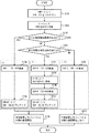
図1は、実施の形態1にかかる半導体システムSYS1の構成を示すブロック図である。本実施の形態にかかる半導体システムSYS1では、制御装置によるモジュールの通信規格情報の取得時、モジュールが、制御装置から通信バスを介して供給される電圧と、モジュールの通信規格に基づいて定められた閾値電圧と、の比較結果を、モジュールの通信規格の情報として制御装置に送信する。それにより、制御装置は、モジュールから取得した通信規格の情報に基づいて、制御装置とモジュールとの間の通信規格を正しく設定することができる。その結果、制御装置とモジュールとの間で正常なデータ通信を行うことができる。以下、具体的に説明する。
<
FIG. 1 is a block diagram of the configuration of the semiconductor system SYS1 according to the first embodiment. In the semiconductor system SYS1 according to the present embodiment, when the communication standard information of the module is acquired by the control device, the module is determined based on the voltage supplied from the control device via the communication bus and the communication standard of the module. The comparison result with the threshold voltage is transmitted to the control device as information on the communication standard of the module. Accordingly, the control device can correctly set the communication standard between the control device and the module based on the communication standard information acquired from the module. As a result, normal data communication can be performed between the control device and the module. This will be specifically described below.
図1に示すように、半導体システムSYS1は、制御装置1と、モジュール(半導体装置)M1と、制御装置1とモジュールM1とを接続する通信バスB1と、を備える。本実施の形態では、制御装置1とモジュールM1とのデータ通信方式として、I2C方式が採用されている場合を例に説明する。したがって、通信バスB1は、少なくとも電源線VDD、接地線GND、クロックの信号線SCL及びデータの信号線SDAにより構成されている。
As illustrated in FIG. 1, the semiconductor system SYS1 includes a
(制御装置1)
制御装置1は、一つ又は複数のチップからなり、制御回路11と、供給電圧切替回路12と、信号電圧設定回路13と、を備える。制御回路11は、例えばマイコンである。
(Control device 1)
The
制御回路11と信号電圧設定回路13とは、通信バスB1に含まれる信号線SDA,SCLを介して接続されている。
The control circuit 11 and the signal
(制御回路11)
制御回路11は、通信バスB1を介して、モジュールM1とデータ通信を行う回路である。なお、制御回路11は、モジュールM1が対応する通信速度で通信する機能を有する。
(Control circuit 11)
The control circuit 11 is a circuit that performs data communication with the module M1 via the communication bus B1. Note that the control circuit 11 has a function of communicating at a communication speed corresponding to the module M1.
また、制御回路11は、供給電圧切替回路12に電圧制御信号S1を出力し、信号電圧設定回路13にイネーブル信号ENBを出力することで、供給電圧切替回路12及び信号電圧設定回路13を制御する。
Further, the control circuit 11 outputs the voltage control signal S1 to the supply
ここで、制御回路11は、通常動作前に、モジュールM1の内部回路の通信規格の情報(以下、単にモジュールM1の通信規格の情報とも称す)を取得したうえで、その通信規格でモジュールM1とデータ通信を行う。なお、本実施の形態では、制御回路11がモジュールM1の通信規格の情報として駆動電圧の情報を取得したうえで、その駆動電圧をモジュールに供給したうえでモジュールM1とデータ通信を行う場合を例に説明する。制御回路11によるモジュールM1の通信規格の情報(ここでは駆動電圧の情報)の取得方法については、後述する。 Here, the control circuit 11 acquires information on the communication standard of the internal circuit of the module M1 (hereinafter, also simply referred to as information on the communication standard of the module M1) before normal operation, and then uses the communication standard as the module M1. Perform data communication. In this embodiment, the control circuit 11 obtains drive voltage information as communication standard information of the module M1, supplies the drive voltage to the module, and performs data communication with the module M1. Explained. A method for acquiring the communication standard information (here, drive voltage information) of the module M1 by the control circuit 11 will be described later.
(供給電圧切替回路12)
供給電圧切替回路12は、電源線VDDに供給する電源電圧を切り替える回路である。例えば、供給電圧切替回路12は、電源VDD1から供給される3.3Vの電源電圧(以下、電源電圧VDD1と称す)、及び、電源VDD2から供給される5Vの電源電圧(以下、電源電圧VDD2と称す)の何れかを、制御回路11からの電圧制御信号S1に基づいて選択し、電源線VDDに対して出力する。
(Supply voltage switching circuit 12)
The supply
図2は、供給電圧切替回路12の構成例を示す回路図である。
図2に示すように、供給電圧切替回路12は、PチャネルMOSトランジスタ(以下、単にトランジスタと称す)MP1,MP2と、インバータINV1と、を有する。
FIG. 2 is a circuit diagram illustrating a configuration example of the supply
As shown in FIG. 2, the supply
トランジスタMP1は、電源VDD2と、電源線VDDと、の間に設けられ、制御回路11からの電圧制御信号S1に応じてオン/オフを制御する。トランジスタMP2は、電源VDD1と、電源線VDDと、の間に設けられ、トランジスタMP1と相補的にオン/オフを制御する。 The transistor MP1 is provided between the power supply VDD2 and the power supply line VDD, and controls on / off according to the voltage control signal S1 from the control circuit 11. The transistor MP2 is provided between the power supply VDD1 and the power supply line VDD, and controls on / off complementarily with the transistor MP1.
例えば、制御回路11からの電圧制御信号S1がHレベルの場合、トランジスタMP1がオフし、トランジスタMP2がオンするため、電源線VDDには、3.3Vの電源電圧VDD1が供給される。他方、制御回路11からの電圧制御信号S1がLレベルの場合、トランジスタMP1がオンし、トランジスタMP2がオフするため、電源線VDDには、5Vの電源電圧VDD2が供給される。 For example, when the voltage control signal S1 from the control circuit 11 is at the H level, the transistor MP1 is turned off and the transistor MP2 is turned on, so that the power supply voltage VDD1 of 3.3 V is supplied to the power supply line VDD. On the other hand, when the voltage control signal S1 from the control circuit 11 is at L level, the transistor MP1 is turned on and the transistor MP2 is turned off, so that the power supply voltage VDD2 of 5V is supplied to the power supply line VDD.
なお、本実施の形態では、供給電圧切替回路12が、2つの電源電圧VDD1,VDD2の何れかを選択的に電源線VDDに供給する場合を例に説明しているが、これに限られない。供給電圧切替回路12は、3つ以上の電源電圧の何れかを選択的に電源線VDDに供給する構成に適宜変更可能である。
In the present embodiment, the case where the supply
(信号電圧設定回路13)
信号電圧設定回路13は、モジュールM1の通信規格情報の取得時、信号線SDA,SCLの電圧レベルを所定の電圧に設定する回路である。例えば、信号電圧設定回路13は、モジュールM1の通信規格情報の取得時、信号線SDA,SCLを何れもLレベルにプルダウンする。
(Signal voltage setting circuit 13)
The signal
図3は、信号電圧設定回路13の構成例を示す回路図である。
図3に示すように、信号電圧設定回路13は、PチャネルMOSトランジスタ(以下、単にトランジスタと称す)MP3,MP4と、抵抗素子R1〜R4と、を有する。なお、プルダウン用の抵抗素子R3,R4の抵抗値は、プルアップ用の抵抗素子R1,R2の抵抗値よりも十分に大きい。
FIG. 3 is a circuit diagram showing a configuration example of the signal
As shown in FIG. 3, the signal
トランジスタMP3は、電源線VDDと、抵抗素子R1の一端と、の間に設けられ、制御回路11からのイネーブル信号ENBに応じてオン/オフを制御する。トランジスタMP4は、電源線VDDと、抵抗素子R2の一端と、の間に設けられ、制御回路11からのイネーブル信号ENBに応じてオン/オフを制御する。抵抗素子R1の他端は、信号線SCLに接続され、抵抗素子R2の他端は、信号線SDAに接続される。抵抗素子R3は、信号線SCLと接地線GNDとの間に設けられている。抵抗素子R4は、信号線SDAと接地線GNDとの間に設けられている。 The transistor MP3 is provided between the power supply line VDD and one end of the resistance element R1, and controls on / off according to the enable signal ENB from the control circuit 11. The transistor MP4 is provided between the power supply line VDD and one end of the resistance element R2, and controls on / off according to the enable signal ENB from the control circuit 11. The other end of the resistance element R1 is connected to the signal line SCL, and the other end of the resistance element R2 is connected to the signal line SDA. The resistance element R3 is provided between the signal line SCL and the ground line GND. The resistance element R4 is provided between the signal line SDA and the ground line GND.
例えば、制御回路11とモジュールM1との間でデータ通信が行われる通常動作時(以下、通常動作モードとも称す)、制御回路11は、Lレベルのイネーブル信号ENBを出力する。それにより、トランジスタMP3,MP4が何れもオンするため、信号線SCL,SDAは何れもHレベルにプルアップされる。他方、制御回路11によるモジュールM1の通信規格情報の取得時(以下、通信規格取得モードとも称す)、制御回路11は、Hレベルのイネーブル信号ENBを出力する。それにより、トランジスタMP3,MP4が何れもオフするため、信号線SCL,SDAはそれぞれ抵抗素子R3,R4によって、Lレベルにプルダウンされる。 For example, during a normal operation in which data communication is performed between the control circuit 11 and the module M1 (hereinafter also referred to as a normal operation mode), the control circuit 11 outputs an L level enable signal ENB. As a result, the transistors MP3 and MP4 are both turned on, so that the signal lines SCL and SDA are both pulled up to the H level. On the other hand, when the control circuit 11 acquires the communication standard information of the module M1 (hereinafter also referred to as a communication standard acquisition mode), the control circuit 11 outputs an H level enable signal ENB. Thereby, the transistors MP3 and MP4 are both turned off, and the signal lines SCL and SDA are pulled down to the L level by the resistance elements R3 and R4, respectively.
通常動作時の制御回路11とモジュールM1とのデータの受け渡し方法を説明する。
通常動作時において、制御回路11からモジュールM1に向けてHレベルの信号SDA(信号線SDAの信号)を送信する場合、制御回路11は、信号電圧設定回路13によってHレベルにプルアップされた信号線SDAの状態を保持する。それにより、モジュールM1には、Hレベルの信号SDAが供給される。また、制御回路11からモジュールM1に向けてLレベルの信号SDAを送信する場合、制御回路11は、信号電圧設定回路13によってHレベルにプルアップされた信号線SDAの電荷を引き抜くことでLレベルにする。それにより、モジュールM1には、Lレベルの信号SDAが供給される。これは、信号SCL(信号線SCLの信号)についても同様のことが言える。
A method of transferring data between the control circuit 11 and the module M1 during normal operation will be described.
During normal operation, when transmitting an H level signal SDA (signal of the signal line SDA) from the control circuit 11 to the module M1, the control circuit 11 is a signal pulled up to the H level by the signal
逆に、通常動作時において、モジュールM1から制御回路11に向けてHレベルの信号SDAを送信する場合、モジュールM1は、信号電圧設定回路13によってHレベルにプルアップされた信号線SDAの状態を保持する。それにより、制御回路11には、Hレベルの信号SDAが供給される。また、モジュールM1から制御回路11に向けてLレベルの信号SDAを送信する場合、モジュールM1は、信号電圧設定回路13によってHレベルにプルアップされた信号線SDAの電荷を引き抜くことでLレベルにする。それにより、制御回路11には、Lレベルの信号SDAが供給される。これは、信号SCLについても同様のことが言える。
On the contrary, in the normal operation, when transmitting the H level signal SDA from the module M1 to the control circuit 11, the module M1 changes the state of the signal line SDA pulled up to the H level by the signal
それに対し、通信規格情報の取得時には、制御回路11は、信号電圧設定回路13によってLレベルにプルダウンされた信号線SDA,SCLの状態を保持する。それにより、モジュールM1には、Lレベルの信号SDA,SCLが供給される。換言すると、(SDA,SCL)=(0,0)となる。
On the other hand, when acquiring the communication standard information, the control circuit 11 holds the state of the signal lines SDA and SCL pulled down to the L level by the signal
なお、本実施の形態では、制御装置1によるモジュールM1の通信規格情報の取得時、信号線SDA,SCLがLレベルにプルダウンされる場合を例に説明しているが、これに限られない。モジュールM1の通信規格の情報を1ビットで表現できるならば、信号線SDA,SCLの何れか1本のみがLレベルにプルダウンされる構成であってもよい。例えば、信号線SDAのみがLレベルにプルダウンされる構成である場合、信号電圧設定回路13は、トランジスタMP4及び抵抗素子R2,R4のみを備えていればよい。
In the present embodiment, the case where the signal lines SDA and SCL are pulled down to the L level when the
(モジュールM1)
モジュールM1は、内部回路14と、規格情報送信部15と、を備える。なお、規格情報送信部15は、モジュールM1の外部に設けられてもよい。即ち、規格情報送信部15は、モジュールM1に対して後付けされたものであってもよい。
(Module M1)
The module M1 includes an
(規格情報送信部15)
規格情報送信部15は、制御装置1によるモジュールM1の通信規格情報取得時、制御装置1から電源線VDDを介して供給される電圧と、閾値電圧と、を比較して、その比較結果を、モジュールM1の通信規格の情報(ここでは駆動電圧の情報)として、通信バスB1を介して制御装置1に送信する。
(Standard information transmitter 15)
The standard
より詳細には、規格情報送信部15は、電圧検知回路16と、規格情報出力回路17と、により構成されている。
More specifically, the standard
(電圧検知回路16)
電圧検知回路16は、制御装置1によるモジュールM1の通信規格情報取得時、制御装置1から電源線VDDを介して供給される電圧が、モジュールM1の通信規格(ここでは駆動電圧)に基づいて定められた閾値電圧より高ければ、検知信号RSTBをアクティブにする(即ち、Hレベルを出力する)。また、制御装置1から電源線VDDを介して供給される電圧が、モジュールM1の通信規格(ここでは駆動電圧)に基づいて定められた閾値電圧より低ければ、検知信号RSTBをインアクティブにする(即ち、Lレベルを出力する)。
(Voltage detection circuit 16)
The
例えば、モジュールM1の駆動電圧が3.3Vの場合、モジュールM1に設けられた電圧検知回路16の閾値電圧は3V程度に設定される。この電圧検知回路16は、制御装置1から電源線VDDを介して3.3Vの電圧VDD1が供給されると、検知信号RSTBをアクティブにする。
For example, when the drive voltage of the module M1 is 3.3V, the threshold voltage of the
また、例えば、モジュールM1の駆動電圧が5Vの場合、モジュールM1に設けられた電圧検知回路16の閾値電圧は4V程度に設定される。この電圧検知回路16は、制御装置1から電源線VDDを介して5Vの電圧VDD2が供給されると、検知信号RSTBをアクティブにする。
For example, when the drive voltage of the module M1 is 5V, the threshold voltage of the
図4は、電圧検知回路16の構成例を示すブロック図である。
図4に示すように、電圧検知回路16は、リセット回路161を有する。リセット回路161は、電源線VDDと接地線GNDとの間に設けられ、電源線VDDの電圧が閾値電圧より高くなると、リセット信号、即ち、検知信号RSTBをLレベルからHレベルに切り替える。
FIG. 4 is a block diagram illustrating a configuration example of the
As shown in FIG. 4, the
(規格情報出力回路17)
規格情報出力回路17は、電圧検知回路16の検知結果から明らかになったモジュールM1の通信規格情報を、通信バスB1に含まれる信号線SDA,SCLを介して、制御装置1に出力する。換言すると、規格情報出力回路17は、電圧検知回路16から出力された検知信号RSTBの状態に応じて通信バスB1に含まれる信号線SDA,SCLの電圧レベルを設定する。
(Standard information output circuit 17)
The standard
図5は、規格情報出力回路17の構成例を示す回路図である。
図5に示すように、規格情報出力回路17は、PチャネルMOSトランジスタ(以下、単にトランジスタと称す)MP5,MP6と、インバータINV2と、抵抗素子R5,R6と、を有する。なお、プルアップ用の抵抗素子R5,R6の抵抗値は、信号電圧設定回路13に設けられたプルアップ用の抵抗素子R1,R2の抵抗値と同等程度であって、信号電圧設定回路13に設けられたプルダウン用の抵抗素子R3,R4の抵抗値よりも十分に小さい。
FIG. 5 is a circuit diagram showing a configuration example of the standard
As shown in FIG. 5, the standard
トランジスタMP5は、電源線VDDと、抵抗素子R5の一端と、の間に設けられ、電圧検知回路16からの検知信号RSTBに応じてオン/オフを制御する。トランジスタMP6は、電源線VDDと、抵抗素子R6の一端と、の間に設けられ、トランジスタMP5と相補的にオン/オフを制御する。抵抗素子R5の他端は、信号線SCLに接続され、抵抗素子R6の他端は、信号線SDAの他端に接続される。
The transistor MP5 is provided between the power supply line VDD and one end of the resistance element R5, and controls on / off according to the detection signal RSTB from the
例えば、電圧検知回路16からの検知信号RSTBがLレベルの場合、トランジスタMP5がオンし、トランジスタMP6がオフするため、信号線SCLはLレベルからHレベルにプルアップされ、信号線SDAはLレベルに保持される。換言すると、(SDA,SCL)=(0,1)となる。
For example, when the detection signal RSTB from the
他方、電圧検知回路16からの検知信号RSTBがHレベルの場合、トランジスタMP5がオフし、トランジスタMP6がオンするため、信号線SCLはLベルに保持され、信号線SDAはLレベルからHレベルにプルアップされる。換言すると、(SDA,SCL)=(1,0)となる。
On the other hand, when the detection signal RSTB from the
要するに、モジュールM1の駆動電圧が3.3Vの場合、規格情報送信部15は、制御装置1から電源線VDDを介して3.3Vの電圧VDD1が供給されると、(SDA,SCL)=(1,0)に設定する。また、モジュールM1の駆動電圧が5Vの場合、規格情報送信部15は、制御装置1から電源線VDDを介して3.3Vの電圧VDD1が供給されると、(SDA,SCL)=(0,1)に設定し、制御装置1から電源線VDDを介して5Vの電圧VDD2が供給されると、(SDA,SCL)=(1,0)に設定する。
In short, when the driving voltage of the module M1 is 3.3V, the standard
(半導体システムSYS1の動作)
続いて、半導体システムSYS1の通信規格設定動作について説明する。
図6は、半導体システムSYS1の通信規格設定動作を示すフローチャートである。
(Operation of the semiconductor system SYS1)
Next, the communication standard setting operation of the semiconductor system SYS1 will be described.
FIG. 6 is a flowchart showing the communication standard setting operation of the semiconductor system SYS1.
図6に示すように、まず、制御回路11は、イネーブル信号ENBをHレベル(ENB=1)にして、動作モードを通信規格取得モードに切り替える。それにより、信号電圧設定回路13に設けられたトランジスタMP3,MP4が何れもオフするため、信号線SDA,SCLは何れもLレベルにプルダウンされる(ステップS101)。それにより、モジュールM1には、Lレベルの信号SDA,SCLが供給される。
As shown in FIG. 6, first, the control circuit 11 sets the enable signal ENB to the H level (ENB = 1) and switches the operation mode to the communication standard acquisition mode. As a result, the transistors MP3 and MP4 provided in the signal
また、制御回路11は、電圧制御信号S1をHレベル(S1=1)にする。それにより、供給電圧切替回路12に設けられたトランジスタMP1がオフし、トランジスタMP2がオンするため、電源線VDDには3.3Vの電源電圧VDD1が供給される(ステップS102)。
Further, the control circuit 11 sets the voltage control signal S1 to the H level (S1 = 1). As a result, the transistor MP1 provided in the supply
(i)モジュールM1の駆動電圧が3.3Vの場合
モジュールM1の駆動電圧が3.3Vの場合、電源線VDDに3.3Vの電源電圧VDD1が供給されると、モジュールM1に設けられた電圧検知回路16は、検知信号RSTBをLレベルからHレベルに切り替える。つまり、RSTB=1となる(ステップS103のYES)。
(i) When the driving voltage of the module M1 is 3.3V When the driving voltage of the module M1 is 3.3V, when the power supply voltage VDD1 of 3.3V is supplied to the power supply line VDD, the voltage provided in the module M1 The
それにより、規格情報出力回路17に設けられたトランジスタMP5がオフし、トランジスタMP6がオンするため、信号線SCLはLレベルに保持され、信号線SDAはLレベルからHレベルにプルアップされる。それにより、制御回路11には、Hレベルの信号SDA及びLレベルの信号SCLが供給される。換言すると、(SDA,SCL)=(1,0)となる(ステップS104)。これにより、制御回路11は、モジュールM1の駆動電圧が3.3Vであると判定する。
As a result, the transistor MP5 provided in the standard
その後、制御回路11は、イネーブル信号ENBをLレベル(ENB=0)にして、動作モードを通常動作モードに切り替える。それにより、信号電圧設定回路13に設けられたトランジスタMP3,MP4が何れもオンするため、信号線SDA,SCLは何れもHレベルにプルアップされる(ステップS105)。
Thereafter, the control circuit 11 sets the enable signal ENB to L level (ENB = 0) and switches the operation mode to the normal operation mode. As a result, the transistors MP3 and MP4 provided in the signal
その後、制御装置1とモジュールM1とは通常動作を開始する(ステップS106)。つまり、制御装置1とモジュールM1との間でデータ通信が開始される。
Thereafter, the
(ii)モジュールM1の駆動電圧が5Vの場合
モジュールM1の駆動電圧が5Vの場合、、電源線VDDに3.3Vの電源電圧VDD1が供給されるとモジュールM1に設けられた電圧検知回路16は、検知信号RSTBをLレベルに保持する。つまり、RSTB=0となる(ステップS103のNO)。
(ii) When the drive voltage of the module M1 is 5V When the drive voltage of the module M1 is 5V, when the power supply voltage VDD1 of 3.3V is supplied to the power supply line VDD, the
それにより、規格情報出力回路17に設けられたトランジスタMP5がオンし、トランジスタMP6がオフするため、信号線SCLはLレベルからHレベルにプルアップされ、信号線SDAはLレベルに保持される。それにより、制御回路11には、Lレベルの信号SDA及びHレベルの信号SCLが供給される。換言すると、(SDA,SCL)=(0,1)となる(ステップS107)。これにより、制御回路11は、モジュールM1の駆動電圧が3.3Vより高いと判定する。
Accordingly, the transistor MP5 provided in the standard
その後、制御回路11は、電圧制御信号S1をLレベル(S1=0)にする。それにより、供給電圧切替回路12に設けられたトランジスタMP1がオンし、トランジスタMP2がオフするため、電源線VDDには5Vの電源電圧VDD2が供給される(ステップS108)。
Thereafter, the control circuit 11 sets the voltage control signal S1 to the L level (S1 = 0). Accordingly, the transistor MP1 provided in the supply
電源線VDDに5Vの電源電圧VDD2が供給されると、モジュールM1に設けられた電圧検知回路16は、検知信号RSTBをLレベルからHレベルに切り替える。つまり、RSTB=1となる。それにより、規格情報出力回路17に設けられたトランジスタMP5がオフし、トランジスタMP6がオンするため、信号線SCLはLレベルに保持され、信号線SDAはLレベルからHレベルにプルアップされる。それにより、制御回路11には、Hレベルの信号SDA及びLレベルの信号SCLが供給される。換言すると、(SDA,SCL)=(1,0)となる(ステップS109)。これにより、制御回路11は、モジュールM1の駆動電圧が5Vであると判定する。
When the power supply voltage VDD2 of 5V is supplied to the power supply line VDD, the
その後、制御回路11は、イネーブル信号ENBをLレベル(ENB=0)にして、動作モードを通常動作モードに切り替える。それにより、信号電圧設定回路13に設けられたトランジスタMP3,MP4が何れもオンするため、信号線SDA,SCLは何れもHレベルにプルアップされる(ステップS110)。
Thereafter, the control circuit 11 sets the enable signal ENB to L level (ENB = 0) and switches the operation mode to the normal operation mode. As a result, the transistors MP3 and MP4 provided in the signal
その後、制御装置1とモジュールM1とは通常動作を開始する(ステップS106)。つまり、制御装置1とモジュールM1との間でデータ通信が開始される。
Thereafter, the
本実施の形態では、モジュールM1が、通信規格情報の一つである駆動電圧の情報を送信し、制御装置1が、その情報に基づいてモジュールM1に供給する駆動電圧を設定する場合を例に説明したが、これに限られない。例えば、モジュールM1が、通信速度等の他の通信規格の情報を送信し、制御装置1が、その情報に基づいて制御装置1とモジュールM1との間の通信規格を設定する構成であってもよい。
In the present embodiment, the case where the module M1 transmits drive voltage information, which is one of the communication standard information, and the
このように、半導体システムSYS1では、制御装置1によるモジュールM1の通信規格情報取得時、モジュールM1が、制御装置1から通信バスB1を介して供給される電圧と、モジュールM1の通信規格に基づいて定められた閾値電圧と、の比較結果を、モジュールM1の通信規格の情報として制御装置1に送信する。それにより、制御装置1は、モジュールM1から取得した通信規格の情報に基づいて、制御装置1とモジュールM1との間の通信規格を正しく設定することができる。その結果、制御装置1とモジュールM1との間で正常なデータ通信を行うことができる。
Thus, in the semiconductor system SYS1, when the communication standard information of the module M1 is acquired by the
<実施の形態2>
図7は、実施の形態2にかかる半導体システムSYS2の構成を示すブロック図である。半導体システムSYS1では、単体のモジュールM1が設けられていたのに対し、半導体システムSYS2では、複数のモジュールM1〜Mn(nは2以上の整数)が設けられている。
<
FIG. 7 is a block diagram of the configuration of the semiconductor system SYS2 according to the second embodiment. The semiconductor system SYS1 is provided with a single module M1, whereas the semiconductor system SYS2 is provided with a plurality of modules M1 to Mn (n is an integer of 2 or more).
モジュールM1〜Mnは何れも同一の通信バスB1に接続されている。半導体システムSYS2のその他の構成については、半導体システムSYS1と同様であるため、その説明を省略する。 The modules M1 to Mn are all connected to the same communication bus B1. Since the other configuration of the semiconductor system SYS2 is the same as that of the semiconductor system SYS1, description thereof is omitted.
(半導体システムSYS2の動作)
続いて、半導体システムSYS2の通信規格設定動作について説明する。
図8は、半導体システムSYS2の通信規格設定動作を示すフローチャートである。
(Operation of the semiconductor system SYS2)
Next, the communication standard setting operation of the semiconductor system SYS2 will be described.
FIG. 8 is a flowchart showing the communication standard setting operation of the semiconductor system SYS2.
図8に示すように、まず、制御回路11は、イネーブル信号ENBをHレベル(ENB=1)にして、動作モードを通信規格取得モードに切り替える。それにより、信号電圧設定回路13に設けられたトランジスタMP3,MP4が何れもオフするため、信号線SDA,SCLは何れもLレベルにプルダウンされる(ステップS101)。それにより、モジュールM1には、Lレベルの信号SDA,SCLが供給される。
As shown in FIG. 8, first, the control circuit 11 sets the enable signal ENB to the H level (ENB = 1) and switches the operation mode to the communication standard acquisition mode. As a result, the transistors MP3 and MP4 provided in the signal
また、制御回路11は、電圧制御信号S1をHレベル(S1=1)にする。それにより、供給電圧切替回路12に設けられたトランジスタMP1がオフし、トランジスタMP2がオンするため、電源線VDDには3.3Vの電源電圧VDD1が供給される(ステップS102)。
Further, the control circuit 11 sets the voltage control signal S1 to the H level (S1 = 1). As a result, the transistor MP1 provided in the supply
(i)全てのモジュールM1〜Mnの駆動電圧が3.3Vの場合
全てのモジュールM1〜Mnの駆動電圧が3.3Vの場合、電源線VDDに3.3Vの電源電圧VDD1が供給されると、各モジュールM1〜Mnに設けられた電圧検知回路16は、検知信号RSTBをLレベルからHレベルに切り替える(RSTB=1)(ステップS103のYES)。
(i) When drive voltages of all modules M1 to Mn are 3.3V When drive voltages of all modules M1 to Mn are 3.3V, when a power supply voltage VDD1 of 3.3V is supplied to the power supply line VDD The
それにより、各モジュールM1〜Mnの規格情報出力回路17に設けられたトランジスタMP5がオフし、トランジスタMP6がオンするため、信号線SCLはLレベルに保持され、信号線SDAはLレベルからHレベルにプルアップされる。それにより、制御回路11には、Hレベルの信号SDA及びLレベルの信号SCLが供給される。換言すると、(SDA,SCL)=(1,0)となる(ステップS104)。これにより、制御回路11は、全てのモジュールM1〜Mnの駆動電圧が3.3Vであると判定する。
As a result, the transistor MP5 provided in the standard
その後、制御回路11は、イネーブル信号ENBをLレベル(ENB=0)にして、動作モードを通常動作モードに切り替える。それにより、信号電圧設定回路13に設けられたトランジスタMP3,MP4が何れもオンするため、信号線SDA,SCLは何れもHレベルにプルアップされる(ステップS105)。
Thereafter, the control circuit 11 sets the enable signal ENB to L level (ENB = 0) and switches the operation mode to the normal operation mode. As a result, the transistors MP3 and MP4 provided in the signal
その後、制御装置1とモジュールM1〜Mnとは通常動作を開始する(ステップS106)。つまり、制御装置1とモジュールM1〜Mnとの間でデータ通信が開始される。なお、各モジュールM1〜Mnは固有のアドレスを持っており、制御装置1がアドレスを指定することで、制御装置1と指定されたアドレスのモジュールとの間でデータ通信が行われる。
Thereafter, the
(ii)全てのモジュールM1〜Mnの駆動電圧が5Vの場合
全てのモジュールM1〜Mnの駆動電圧が5Vの場合、電源線VDDに3.3Vの電源電圧VDD1が供給されると、各モジュールM1〜Mnに設けられた電圧検知回路16は、検知信号RSTBをLレベルに保持する(RSTB=0)(ステップS103のNO→ステップS201のYES)。
(ii) When drive voltages of all modules M1 to Mn are 5V When drive voltages of all modules M1 to Mn are 5V, when a power supply voltage VDD1 of 3.3V is supplied to the power supply line VDD, each module M1 The
それにより、各モジュールM1〜Mnの規格情報出力回路17に設けられたトランジスタMP5がオンし、トランジスタMP6がオフするため、信号線SCLはLレベルからHレベルにプルアップされ、信号線SDAはLレベルに保持される。それにより、制御回路11には、Lレベルの信号SDA及びHレベルの信号SCLが供給される。換言すると、(SDA,SCL)=(0,1)となる(ステップS107)。これにより、制御回路11は、全てのモジュールM1〜Mnの駆動電圧が3.3Vより大きいと判定する。
As a result, the transistor MP5 provided in the standard
その後、制御回路11は、電圧制御信号S1をLレベル(S1=0)にする。それにより、供給電圧切替回路12に設けられたトランジスタMP1がオンし、トランジスタMP2がオフするため、電源線VDDには5Vの電源電圧VDD2が供給される(ステップS108)。
Thereafter, the control circuit 11 sets the voltage control signal S1 to the L level (S1 = 0). Accordingly, the transistor MP1 provided in the supply
電源線VDDに5Vの電源電圧VDD2が供給されると、各モジュールM1〜Mnに設けられた電圧検知回路16は、検知信号RSTBをLレベルからHレベルに切り替える。つまり、RSTB=1となる。それにより、各モジュールM1〜Mnの規格情報出力回路17に設けられたトランジスタMP5がオフし、トランジスタMP6がオンするため、信号線SDAはLレベルからHレベルにプルアップされ、信号線SCLはLレベルに保持される。それにより、制御回路11には、Hレベルの信号SDA及びLレベルの信号SCLが供給される。換言すると、(SDA,SCL)=(1,0)となる(ステップS109)。これにより、制御回路11は、全てのモジュールM1〜Mnの駆動電圧が5Vであると判定する。
When the power supply voltage VDD2 of 5V is supplied to the power supply line VDD, the
その後、制御回路11は、イネーブル信号ENBをLレベル(ENB=0)にして、動作モードを通常動作モードに切り替える。それにより、信号電圧設定回路13に設けられたトランジスタMP3,MP4が何れもオンするため、信号線SDA,SCLは何れもHレベルにプルアップされる(ステップS110)。
Thereafter, the control circuit 11 sets the enable signal ENB to L level (ENB = 0) and switches the operation mode to the normal operation mode. As a result, the transistors MP3 and MP4 provided in the signal
その後、制御装置1とモジュールM1〜Mnとは通常動作を開始する(ステップS106)。つまり、制御装置1とモジュールM1〜Mnとの間でデータ通信が開始される。なお、各モジュールM1〜Mnは固有のアドレスを持っており、制御装置1がアドレスを指定することで、制御装置1と指定されたアドレスのモジュールとの間でデータ通信が行われる。
Thereafter, the
(iii)モジュールM1〜Mnの一部の駆動電圧が3.3V、残りが5Vの場合
モジュールM1〜Mnの一部の駆動電圧が3.3V、モジュールM1〜Mnの残りの駆動電圧が5Vの場合、3.3Vの駆動電圧のモジュールでは検知信号RSTBがHレベルになり、5Vの駆動電圧のモジュールでは検知信号RSTBがLレベルに保持される(ステップS103のNO→ステップS201のNO)。
(iii) When a part of the driving voltages of the modules M1 to Mn is 3.3V and the remaining is 5V, a part of the driving voltages of the modules M1 to Mn is 3.3V, and the remaining driving voltage of the modules M1 to Mn is 5V In this case, the detection signal RSTB is at the H level in the 3.3V drive voltage module, and the detection signal RSTB is held at the L level in the 5V drive voltage module (NO in step S103 → NO in step S201).
そのため、3.3Vの駆動電圧のモジュールでは、ステップS104での処理と同様に、信号線SDAがHレベルにプルアップされ、5Vの駆動電圧のモジュールでは、ステップS107での処理と同様に、信号線SCLがHレベルにプルアップされる。それにより、制御回路11には、Hレベルの信号SDA,SCLが供給される。換言すると、(SDA,SCL)=(1,1)となる(ステップS202)。これにより、制御回路11は、モジュールM1〜Mnの駆動電圧が同じでないと判定する。 Therefore, in the 3.3V drive voltage module, the signal line SDA is pulled up to the H level in the same manner as in step S104, and in the 5V drive voltage module, the signal is output in the same manner as in step S107. Line SCL is pulled up to the H level. As a result, H level signals SDA and SCL are supplied to the control circuit 11. In other words, (SDA, SCL) = (1, 1) (step S202). Thereby, the control circuit 11 determines that the drive voltages of the modules M1 to Mn are not the same.
この場合、制御装置1とモジュールM1の間でデータ通信は行われない(ステップS203)。
In this case, data communication is not performed between the
本実施の形態では、各モジュールM1〜Mnが、通信規格情報の一つである駆動電圧の情報を送信し、制御装置1が、その情報に基づいて各モジュールM1〜Mnに供給する駆動電圧を設定する場合を例に説明したが、これに限られない。例えば、各モジュールM1〜Mnが、通信速度等の他の通信規格の情報を送信し、制御装置1が、その情報に基づいて各モジュールM1〜Mnとの間の通信規格を設定する構成であってもよい。
In the present embodiment, each module M1 to Mn transmits drive voltage information which is one of the communication standard information, and the
このように、半導体システムSYS2では、制御装置1によるモジュールM1〜Mnの通信規格情報取得時、各モジュールM1〜Mnが、制御装置1から通信バスB1を介して供給される電圧と閾値電圧との比較結果を、通信規格の情報として制御装置1に送信する。それにより、制御装置1は、モジュールM1〜Mnから取得した通信規格の情報に基づいて、モジュールM1〜Mnとの間の通信規格を正しく設定することができる。その結果、制御装置1とモジュールM1〜Mnとの間で正常なデータ通信を行うことができる。
Thus, in the semiconductor system SYS2, when the communication standard information of the modules M1 to Mn is acquired by the
また、半導体システムSYS2では、モジュールM1〜Mnに通信規格の異なるモジュールが存在する場合、制御装置1と各モジュールM1〜Mnとの間のデータ通信を行わない。それにより、データ通信の誤動作、及び、定格電圧以上の駆動電圧が供給されることによるモジュールの破壊を防ぐことができる。
Further, in the semiconductor system SYS2, when the modules M1 to Mn include modules having different communication standards, the data communication between the
さらに、半導体システムSYS2では、各モジュールM1〜Mnの通信規格の情報が、追加の信号線を用いずに、既存の通信バスB1を介して制御装置1に伝達される。そのため、配線数の増大を防ぐことができる。
Further, in the semiconductor system SYS2, information on the communication standards of the modules M1 to Mn is transmitted to the
(関連技術との差異)
なお、特許文献1の構成では、電源電圧供給部から複数の機器のそれぞれに対して電源電圧を供給しようとした場合、電源電圧供給部と、複数の機器のそれぞれと、を接続する複数の制御信号線が必要になるため、配線数が増大してしまう。他方、複数の機器を一つの制御信号線に接続しようとすると、複数の機器のそれぞれの合成抵抗が合成されてしまうため、電源電圧供給部が各モジュールM1〜Mnの合成抵抗(電源電圧情報)を正しく読み取ることができなくなってしまう。それに対し、半導体システムSYS2は、上記したように、配線数を増大させることなく、制御装置1と各モジュールM1〜Mnの通信規格を正しく設定することができる。
(Differences from related technologies)
In the configuration of
<実施の形態3>
図9は、実施の形態3にかかる半導体システムSYS3の構成を示すブロック図である。半導体システムSYS2では、3.3Vの駆動電圧のモジュールと、5Vの駆動電圧のモジュールと、が通信バスB1に接続されている場合、制御装置1は何れのモジュールともデータ通信を行わなかった。それに対し、半導体システムSYS3では、制御装置1は、一方の駆動電圧(第1通信規格)のモジュールへの電圧供給を停止することで、他方の駆動電圧(第2通信規格)のモジュールとのデータ通信を可能にしている。以下、具体的に説明する。
<
FIG. 9 is a block diagram of a configuration of the semiconductor system SYS3 according to the third embodiment. In the semiconductor system SYS2, when the 3.3V drive voltage module and the 5V drive voltage module are connected to the communication bus B1, the
半導体システムSYS3では、半導体システムSYS2と比較して、各モジュールM1〜Mnが、待機状態設定回路18及び電源接続スイッチ(電源スイッチ)19をさらに備える。
In the semiconductor system SYS3, each module M1 to Mn further includes a standby
以下、各モジュールM1〜Mnを代表してモジュールM1に設けられた待機状態設定回路18及び電源接続スイッチ19について説明するが、モジュールM2〜Mnについても同様である。
Hereinafter, the standby
待機状態設定回路18は、制御回路11からの要求に応じてモジュールM1に対して駆動電圧を供給するか否かを制御する回路である。電源接続スイッチ19は、待機状態設定回路18からの制御信号により電源線VDDと自己の電源電圧端子との導通/非導通を切り替える回路である。
The standby
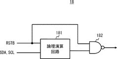
図10は、待機状態設定回路18の構成例を示すブロック図である。
図10に示すように、待機状態設定回路18は、論理演算回路181及び否定論理積回路(以下、単にNAND回路と称す)182と、を有する。
FIG. 10 is a block diagram illustrating a configuration example of the standby
As shown in FIG. 10, the standby
論理演算回路181は、検知信号RSTB及び信号SDA,SCLの値を論理演算した結果を出力する。NAND回路182は、論理演算回路181の出力と、検知信号RSTBと、の否定論理積を、待機状態設定回路18の制御信号として出力する。
The
例えば、待機状態設定回路18は、以下に示す(a),(b),(c)の処理を行う。
(a)検知信号RSTBがLレベルの場合、待機状態設定回路18はHレベルの制御信号を出力する。(b)電源投入時の初期状態において検知信号RSTBがHレベル、信号SDAがHレベル、信号SCLがHレベルの場合に、信号SCLがLレベルに切り替わると、電源が再投入されるまで、論理演算回路181の出力がHレベルに固定されるため、待機状態設定回路18は制御信号をLレベルに固定する。(c)電源投入時の初期状態において検知信号RSTBがHレベル、信号SDAがHレベル、信号SCLがHレベルの場合に、信号SDAがLレベルに切り替わると、電源が再投入されるまで、論理演算回路181の出力がLレベルに固定されるため、待機状態設定回路18は制御信号をHレベルに固定する。
For example, the standby
(A) When the detection signal RSTB is at L level, the standby
図11は、電源接続スイッチ19の構成例を示す回路図である。
図11に示すように、電源接続スイッチ19は、PチャネルMOSトランジスタ(以下、単にトランジスタと称す)MP7を有する。
FIG. 11 is a circuit diagram showing a configuration example of the
As shown in FIG. 11, the
トランジスタMP7は、電源線VDDと、モジュールM1の電源電圧端子と、の間に設けられ、待機状態設定回路18からの制御信号に応じてオン/オフを切り替える。例えば、待機状態設定回路18からの制御信号がLレベルの場合、トランジスタMP7がオンするため、電源線VDDと、モジュールM1の電源電圧端子と、が導通する。他方、待機状態設定回路18からの制御信号がHレベルの場合、トランジスタMP7がオフするため、電源線VDDと、モジュールM1の電源電圧端子と、は導通しない。
The transistor MP7 is provided between the power supply line VDD and the power supply voltage terminal of the module M1, and switches on / off according to a control signal from the standby
なお、本実施の形態では、電源接続スイッチ19が電源線VDDにのみ設けられた場合について説明しているが、これに限られない。電源接続スイッチ19は、信号線SDA,SCLに設けられてもよい。
In the present embodiment, the case where the power
(半導体システムSYS3の動作)
続いて、半導体システムSYS3の通信規格設定動作について説明する。
図12、図13及び図14は、半導体システムSYS3の通信規格設定動作を示すフローチャートである。
(Operation of the semiconductor system SYS3)
Next, the communication standard setting operation of the semiconductor system SYS3 will be described.
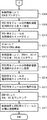
12, 13 and 14 are flowcharts showing the communication standard setting operation of the semiconductor system SYS3.
まず、制御回路11は、イネーブル信号ENBをHレベル(ENB=1)にして、動作モードを通信規格取得モードに切り替える。それにより、信号電圧設定回路13に設けられたトランジスタMP3,MP4が何れもオフするため、信号線SDA,SCLは何れもLレベルにプルダウンされる(図12のステップS101)。それにより、モジュールM1には、Lレベルの信号SDA,SCLが供給される。
First, the control circuit 11 sets the enable signal ENB to the H level (ENB = 1) and switches the operation mode to the communication standard acquisition mode. As a result, the transistors MP3 and MP4 provided in the signal
また、制御回路11は、電圧制御信号S1をHレベル(S1=1)にする。それにより、供給電圧切替回路12に設けられたトランジスタMP1がオフし、トランジスタMP2がオンするため、電源線VDDには3.3Vの電源電圧VDD1が供給される(図12のステップS102)。
Further, the control circuit 11 sets the voltage control signal S1 to the H level (S1 = 1). Accordingly, the transistor MP1 provided in the supply
(i)全てのモジュールM1〜Mnの駆動電圧が3.3Vの場合
全てのモジュールM1〜Mnの駆動電圧が3.3Vの場合、電源線VDDに3.3Vの電源電圧VDD1が供給されると、各モジュールM1〜Mnに設けられた電圧検知回路16は、検知信号RSTBをLレベルからHレベルに切り替える(RSTB=1)(図12のステップS103のYES)。
(i) When drive voltages of all modules M1 to Mn are 3.3V When drive voltages of all modules M1 to Mn are 3.3V, when a power supply voltage VDD1 of 3.3V is supplied to the power supply line VDD The
それにより、各モジュールM1〜Mnの規格情報出力回路17に設けられたトランジスタMP5がオフし、トランジスタMP6がオンするため、信号線SCLはLレベルに保持され、信号線SDAはLレベルからHレベルにプルアップされる。それにより、制御回路11には、Hレベルの信号SDA及びLレベルの信号SCLが供給される。換言すると、(SDA,SCL)=(1,0)となる(図13のステップS104)。これにより、制御回路11は、全てのモジュールM1〜Mnの駆動電圧が3.3Vであると判定する。
As a result, the transistor MP5 provided in the standard
その後、制御回路11は、信号SDA,SCLをHレベルに設定後、信号SCLをHレベルからLレベルにプルダウンする(図13のステップS401)。それにより、各モジュールM1〜Mnの待機状態設定回路18は、上記(b)の処理を行うため、制御信号をLレベルに固定する(図13のステップS402)。それにより、各モジュールM1〜Mnの電源接続スイッチ19がオンするため(図13のステップS403)、全てのモジュールM1〜Mnの内部回路14には、電源線VDDを介して3.3Vの電源電圧VDD1が供給される。
Thereafter, the control circuit 11 sets the signals SDA and SCL to the H level, and then pulls down the signal SCL from the H level to the L level (step S401 in FIG. 13). Accordingly, the standby
その後、制御回路11は、イネーブル信号ENBをLレベル(ENB=0)にして、動作モードを通常動作モードに切り替える。それにより、信号電圧設定回路13に設けられたトランジスタMP3,MP4が何れもオンするため、信号線SDA,SCLは何れもHレベルにプルアップされる(図13のステップS105)。
Thereafter, the control circuit 11 sets the enable signal ENB to L level (ENB = 0) and switches the operation mode to the normal operation mode. As a result, the transistors MP3 and MP4 provided in the signal
その後、制御装置1とモジュールM1〜Mnとは通常動作を開始する(図13のステップS106)。つまり、制御装置1とモジュールM1〜Mnとの間でデータ通信が開始される。
Thereafter, the
(ii)全てのモジュールM1〜Mnの駆動電圧が5Vの場合
全てのモジュールM1〜Mnの駆動電圧が5Vの場合、電源線VDDに3.3Vの電源電圧VDD1が供給されると、各モジュールM1〜Mnに設けられた電圧検知回路16は、検知信号RSTBをLレベルに保持する(RSTB=0)(図12のステップS103のNO→ステップS201のYES)。
(ii) When drive voltages of all modules M1 to Mn are 5V When drive voltages of all modules M1 to Mn are 5V, when a power supply voltage VDD1 of 3.3V is supplied to the power supply line VDD, each module M1 The
それにより、各モジュールM1〜Mnの規格情報出力回路17に設けられたトランジスタMP5がオンし、トランジスタMP6がオフするため、信号線SCLはLレベルからHレベルにプルアップされ、信号線SDAはLレベルに保持される。それにより、制御回路11には、Lレベルの信号SDA及びHレベルの信号SCLが供給される。換言すると、(SDA,SCL)=(0,1)となる(図13のステップS107)。これにより、制御回路11は、全てのモジュールM1〜Mnの駆動電圧が3.3Vより大きいと判定する。
As a result, the transistor MP5 provided in the standard
その後、制御回路11は、電圧制御信号S1をLレベル(S1=0)にする。それにより、供給電圧切替回路12に設けられたトランジスタMP1がオンし、トランジスタMP2がオフするため、電源線VDDには5Vの電源電圧VDD2が供給される(図13のステップS108)。
Thereafter, the control circuit 11 sets the voltage control signal S1 to the L level (S1 = 0). Accordingly, the transistor MP1 provided in the supply
電源線VDDに5Vの電源電圧VDD2が供給されると、各モジュールM1〜Mnに設けられた電圧検知回路16は、検知信号RSTBをLレベルからHレベルに切り替える。つまり、RSTB=1となる。それにより、各モジュールM1〜Mnの規格情報出力回路17に設けられたトランジスタMP5がオフし、トランジスタMP6がオンするため、信号線SDAはLレベルからHレベルにプルアップされ、信号線SCLはLレベルに保持される。それにより、制御回路11には、Hレベルの信号SDA及びLレベルの信号SCLが供給される。換言すると、(SDA,SCL)=(1,0)となる(図13のステップS109)。これにより、制御回路11は、全てのモジュールM1〜Mnの駆動電圧が5Vであると判定する。
When the power supply voltage VDD2 of 5V is supplied to the power supply line VDD, the
その後、制御回路11は、信号SDA,SCLをHレベルに設定後、信号SCLをHレベルからLレベルにプルダウンする(図13のステップS404)。それにより、各モジュールM1〜Mnの待機状態設定回路18は、上記(b)の処理を行うため、制御信号をLレベルに固定する(図13のステップS405)。それにより、各モジュールM1〜Mnの電源接続スイッチ19がオンするため(図13のステップS406)、全てのモジュールM1〜Mnの内部回路14には、電源線VDDを介して5Vの電源電圧VDD2が供給される。
Thereafter, the control circuit 11 sets the signals SDA and SCL to the H level, and then pulls down the signal SCL from the H level to the L level (step S404 in FIG. 13). Thereby, the standby
その後、制御回路11は、イネーブル信号ENBをLレベル(ENB=0)にして、動作モードを通常動作モードに切り替える。それにより、信号電圧設定回路13に設けられたトランジスタMP3,MP4が何れもオンするため、信号線SDA,SCLは何れもHレベルにプルアップされる(図13のステップS110)。
Thereafter, the control circuit 11 sets the enable signal ENB to L level (ENB = 0) and switches the operation mode to the normal operation mode. As a result, the transistors MP3 and MP4 provided in the signal
その後、制御回路11とモジュールM1とは通常動作を開始する(図13のステップS106)。つまり、制御回路11とモジュールM1との間でデータ通信が開始される。 Thereafter, the control circuit 11 and the module M1 start normal operation (step S106 in FIG. 13). That is, data communication is started between the control circuit 11 and the module M1.
(iii)モジュールM1〜Mnの一部の駆動電圧が3.3V、残りが5Vの場合
モジュールM1〜Mnの一部の駆動電圧が3.3V、モジュールM1〜Mnの残りの駆動電圧が5Vの場合、3.3Vの駆動電圧のモジュールでは検知信号RSTBがHレベルになり、5Vの駆動電圧のモジュールでは検知信号RSTBがLレベルに保持される(図12のステップS103のNO→ステップS201のNO)。
(iii) When a part of the driving voltages of the modules M1 to Mn is 3.3V and the remaining is 5V, a part of the driving voltages of the modules M1 to Mn is 3.3V, and the remaining driving voltage of the modules M1 to Mn is 5V In this case, the detection signal RSTB is at the H level in the 3.3V drive voltage module, and the detection signal RSTB is held at the L level in the 5V drive voltage module (NO in step S103 in FIG. 12 → NO in step S201). ).
そのため、3.3Vの駆動電圧のモジュールでは、ステップS104での処理と同様に、信号線SDAがHレベルにプルアップされ、5Vの駆動電圧のモジュールでは、ステップS107での処理と同様に、信号線SCLがHレベルにプルアップされる。それにより、制御回路11には、Hレベルの信号SDA,SCLが供給される。換言すると、(SDA,SCL)=(1,1)となる(図12のステップS202)。これにより、制御回路11は、モジュールM1〜Mnの駆動電圧が同じでないと判定する。 Therefore, in the 3.3V drive voltage module, the signal line SDA is pulled up to the H level in the same manner as in step S104, and in the 5V drive voltage module, the signal is output in the same manner as in step S107. Line SCL is pulled up to the H level. As a result, H level signals SDA and SCL are supplied to the control circuit 11. In other words, (SDA, SCL) = (1, 1) (step S202 in FIG. 12). Thereby, the control circuit 11 determines that the drive voltages of the modules M1 to Mn are not the same.
ここで、モジュールM1〜Mnのうち何れの駆動電圧のモジュールを使用するかを決定する(図12のステップS301)。 Here, it is determined which of the modules M1 to Mn is to be used with which drive voltage (step S301 in FIG. 12).
例えば、3.3Vの駆動電圧のモジュールを使用する場合(図12のステップS301のYES)、制御回路11は、信号SCLをHレベルからLレベルにプルダウンする(図12のステップS302)。それにより、3.3Vの駆動電圧の各モジュールに設けられた待機状態設定回路18は、上記(b)の処理を行うため、制御信号をLレベルに固定する(図12のステップS303)。それにより、3.3Vの駆動電圧の各モジュールに設けられた電源接続スイッチ19がオンするため(図12のステップS304)、3.3Vの駆動電圧の各モジュールには、電源線VDDを介して3.3Vの電源電圧VDD1が供給される。
For example, when a module having a drive voltage of 3.3 V is used (YES in step S301 in FIG. 12), the control circuit 11 pulls down the signal SCL from the H level to the L level (step S302 in FIG. 12). Thereby, the standby
なお、このとき、5Vの駆動電圧の各モジュールでは、検知信号RSTBがLレベルに保持されている。したがって、5Vの駆動電圧の各モジュールに設けられた待機状態設定回路18は、上記(a)の処理を行うため、Hレベルの制御信号を出力している。それにより、5Vの駆動電圧の各モジュールに設けられた電源接続スイッチ19がオフするため、5Vの駆動電圧の各モジュールに電源電圧は供給されない。
At this time, the detection signal RSTB is held at the L level in each module of the drive voltage of 5V. Therefore, the standby
つまり、モジュールM1〜Mnのうち3.3Vの駆動電圧のモジュールのみ動作可能な状態となる(図12のステップS305)。 That is, only the module having a drive voltage of 3.3 V among the modules M1 to Mn can be operated (step S305 in FIG. 12).
その後、制御回路11は、イネーブル信号ENBをLレベル(ENB=0)にして、動作モードを通常動作モードに切り替える。それにより、信号電圧設定回路13に設けられたトランジスタMP3,MP4が何れもオンするため、信号線SDA,SCLは何れもHレベルにプルアップされる(図12のステップS306)。
Thereafter, the control circuit 11 sets the enable signal ENB to L level (ENB = 0) and switches the operation mode to the normal operation mode. As a result, the transistors MP3 and MP4 provided in the signal
その後、制御装置1と3.3Vの駆動電圧のモジュールとは通常動作を開始する(図12のステップS307)。つまり、制御装置1と3.3Vの駆動電圧のモジュールとの間でデータ通信が開始される。
Thereafter, the
一方、5Vの駆動電圧のモジュールを使用する場合(図12のステップS301のNO)、制御回路11は、信号SDAをHレベルからLレベルにプルダウンする(図14のステップS308)。それにより、3.3Vの駆動電圧の各モジュールに設けられた待機状態設定回路18は、上記(c)の処理を行うため、制御信号をHレベルに固定する(図14のステップS309)。それにより、3.3Vの駆動電圧の各モジュールに設けられた電源接続スイッチ19がオフするため(図14のステップS310)、3.3Vの駆動電圧の各モジュールに電源電圧は供給されない。
On the other hand, when a module with a driving voltage of 5 V is used (NO in step S301 in FIG. 12), the control circuit 11 pulls down the signal SDA from the H level to the L level (step S308 in FIG. 14). Thereby, the standby
その後、制御回路11は、電圧制御信号S1をLレベル(S1=0)にする。それにより、供給電圧切替回路12に設けられたトランジスタMP1がオンし、トランジスタMP2がオフするため、電源線VDDには5Vの電源電圧VDD2が供給される(図14のステップS311)。また、それにより、5Vの駆動電圧の各モジュールでは、検知信号RSTBがHレベルになる。
Thereafter, the control circuit 11 sets the voltage control signal S1 to the L level (S1 = 0). As a result, the transistor MP1 provided in the supply
その後、制御回路11は、信号SDA,SCLをHレベルに設定後、信号SCLをHレベルからLレベルにプルダウンする(図14のステップS312)。それにより、5Vの駆動電圧の各モジュールに設けられた待機状態設定回路18は、上記(b)の処理を行うため、制御信号をLレベルに固定する(図14のステップS313)。それにより、5Vの駆動電圧の各モジュールに設けられた電源接続スイッチ19がオンするため(図14のステップS314)、5Vの駆動電圧の各モジュールには、電源線VDDを介して5Vの電源電圧VDD2が供給される。
Thereafter, the control circuit 11 sets the signals SDA and SCL to H level, and then pulls down the signal SCL from H level to L level (step S312 in FIG. 14). As a result, the standby
つまり、モジュールM1〜Mnのうち5Vの駆動電圧のモジュールのみ動作可能な状態となる(図14のステップS315)。 That is, only the module having a driving voltage of 5 V among the modules M1 to Mn can be operated (step S315 in FIG. 14).
その後、制御回路11は、イネーブル信号ENBをLレベル(ENB=0)にして、動作モードを通常動作モードに切り替える。それにより、信号電圧設定回路13に設けられたトランジスタMP3,MP4が何れもオンするため、信号線SDA,SCLは何れもHレベルにプルアップされる(図14のステップS316)。
Thereafter, the control circuit 11 sets the enable signal ENB to L level (ENB = 0) and switches the operation mode to the normal operation mode. As a result, the transistors MP3 and MP4 provided in the signal
その後、制御装置1と5Vの駆動電圧のモジュールとは通常動作を開始する(図14のステップS317)。つまり、制御装置1と5Vの駆動電圧のモジュールとの間でデータ通信が開始される。
Thereafter, the
このように、半導体システムSYS3では、制御装置1によるモジュールM1〜Mnの通信規格情報取得時、各モジュールM1〜Mnが、制御装置1から通信バスB1を介して供給される電圧と閾値電圧との比較結果を、通信規格の情報として制御装置1に送信する。それにより、制御装置1は、モジュールM1〜Mnから取得した通信規格の情報に基づいて、モジュールM1〜Mnとの間の通信規格を正しく設定することができる。その結果、制御装置1とモジュールM1〜Mnとの間で正常なデータ通信を行うことができる。
As described above, in the semiconductor system SYS3, when the communication standard information of the modules M1 to Mn is acquired by the
また、半導体システムSYS3では、モジュールM1〜Mnに通信規格の異なるモジュールが存在する場合でも、制御装置1と、何れか一種類の通信規格のモジュールのみと、の間でデータ通信を行うことができる。
Further, in the semiconductor system SYS3, even when modules having different communication standards exist among the modules M1 to Mn, data communication can be performed between the
さらに、半導体システムSYS2では、各モジュールM1〜Mnの通信規格の情報が、追加の信号線を用いずに、既存の通信バスB1を介して制御装置1に伝達される。そのため、配線数の増大を防ぐことができる。
Further, in the semiconductor system SYS2, information on the communication standards of the modules M1 to Mn is transmitted to the
以上のように、上記実施の形態1〜3にかかる半導体システムでは、制御装置によるモジュールの通信規格情報取得時、モジュールが、制御装置から通信バスを介して供給される電圧と閾値電圧との比較結果を、通信規格の情報として制御装置に送信する。それにより、制御装置は、モジュールから取得した通信規格の情報に基づいて、モジュールとの間の通信規格を正しく設定することができる。その結果、制御装置とモジュールとの間で正常なデータ通信を行うことができる。 As described above, in the semiconductor system according to the first to third embodiments, when the communication standard information of the module is acquired by the control device, the module compares the voltage supplied from the control device via the communication bus with the threshold voltage. The result is transmitted to the control device as communication standard information. Accordingly, the control device can correctly set the communication standard with the module based on the communication standard information acquired from the module. As a result, normal data communication can be performed between the control device and the module.
また、上記実施の形態2,3にかかる半導体システムでは、モジュールが複数存在する場合でも、追加の信号線が不要であるため、配線数の増大を防ぐことができる。 Further, in the semiconductor system according to the second and third embodiments, even when there are a plurality of modules, an additional signal line is not necessary, so that an increase in the number of wirings can be prevented.
以上、本発明者によってなされた発明を実施の形態に基づき具体的に説明したが、本発明は既に述べた実施の形態に限定されるものではなく、その要旨を逸脱しない範囲において種々の変更が可能であることはいうまでもない。 As mentioned above, the invention made by the present inventor has been specifically described based on the embodiments. However, the present invention is not limited to the embodiments already described, and various modifications can be made without departing from the scope of the invention. It goes without saying that it is possible.
例えば、上記の実施の形態に係る半導体装置では、半導体基板、半導体層、拡散層(拡散領域)などの導電型(p型もしくはn型)を反転させた構成としてもよい。そのため、n型、及びp型の一方の導電型を第1の導電型とし、他方の導電型を第2の導電型とした場合、第1の導電型をp型、第2の導電型をn型とすることもできるし、反対に第1の導電型をn型、第2の導電型をp型とすることもできる。 For example, the semiconductor device according to the above embodiment may have a configuration in which conductivity types (p-type or n-type) such as a semiconductor substrate, a semiconductor layer, and a diffusion layer (diffusion region) are inverted. Therefore, when one of n-type and p-type conductivity is the first conductivity type and the other conductivity type is the second conductivity type, the first conductivity type is p-type and the second conductivity type is The first conductivity type may be n-type and the second conductivity type may be p-type.
1 制御装置
11 制御回路
12 供給電圧切替回路
13 信号電圧設定回路
14 内部回路
15 規格情報送信部
16 電圧検知回路
17 規格情報出力回路
18 待機状態設定回路
19 電源接続スイッチ
161 リセット回路
181 論理演算回路
182 否定論理積回路
INV1 インバータ
INV2 インバータ
M1〜Mn モジュール
MP1〜MP7 トランジスタ
R1〜R6 抵抗素子
SYS1 半導体システム
SYS2 半導体システム
SYS3 半導体システム
DESCRIPTION OF
Claims (6)
外部に設けられた制御装置から供給される電圧と、内部回路の通信規格に基づいて定められた閾値電圧と、の比較結果を、前記内部回路の通信規格の情報として当該制御装置に送信する、規格情報送信部と、を備え、
前記通信規格の情報は、前記内部回路の駆動電圧の情報である、半導体装置。 Internal circuitry,
A comparison result between the voltage supplied from the control device provided outside and the threshold voltage determined based on the communication standard of the internal circuit is transmitted to the control device as information on the communication standard of the internal circuit. A standard information transmission unit ,
The information of the communication standard is a semiconductor device , which is information of a driving voltage of the internal circuit .
前記制御装置から供給される電圧が前記閾値電圧より高くなると検知信号をアクティブに切り替える電圧検知回路と、
前記検知信号の状態に応じて、前記内部回路と前記制御装置との間に設けられた信号線の電圧レベルを、前記比較結果に設定する規格情報出力回路と、を有する、請求項1に記載の半導体装置。 The standard information transmission unit
A voltage detection circuit that switches a detection signal to active when a voltage supplied from the control device becomes higher than the threshold voltage;
2. A standard information output circuit that sets a voltage level of a signal line provided between the internal circuit and the control device in the comparison result according to a state of the detection signal. Semiconductor device.
前記制御装置と、
前記制御装置と前記一又は複数の半導体装置夫々とを接続する信号線と、
を備えた半導体システム。 One or more semiconductor devices according to claim 1;
The control device;
A signal line connecting the control device and each of the one or more semiconductor devices;
A semiconductor system with
前記制御装置と、
前記制御装置と、前記第1及び前記第2通信規格の半導体装置と、を接続する信号線と、を備え、
前記第1及び前記第2通信規格の半導体装置の一方に設けられた前記電源スイッチはオンに制御され、前記第1及び前記第2通信規格の半導体装置の他方に設けられた前記電源スイッチはオフに制御される、半導体システム。 A semiconductor device of the first communication standard according to claim 3 and a semiconductor device of a second communication standard different from the first communication standard,
The control device;
A signal line for connecting the control device and the semiconductor devices of the first and second communication standards;
The power switch provided in one of the first and second communication standard semiconductor devices is controlled to be on, and the power switch provided in the other of the first and second communication standard semiconductor devices is off. Controlled by a semiconductor system.
Priority Applications (2)
| Application Number | Priority Date | Filing Date | Title |
|---|---|---|---|
| JP2014266206A JP6341852B2 (en) | 2014-12-26 | 2014-12-26 | Semiconductor device and semiconductor system including the same |
| US14/925,366 US9819518B2 (en) | 2014-12-26 | 2015-10-28 | Semiconductor device, semiconductor system including the same, and control method of semiconductor device |
Applications Claiming Priority (1)
| Application Number | Priority Date | Filing Date | Title |
|---|---|---|---|
| JP2014266206A JP6341852B2 (en) | 2014-12-26 | 2014-12-26 | Semiconductor device and semiconductor system including the same |
Publications (3)
| Publication Number | Publication Date |
|---|---|
| JP2016126488A JP2016126488A (en) | 2016-07-11 |
| JP2016126488A5 JP2016126488A5 (en) | 2017-07-06 |
| JP6341852B2 true JP6341852B2 (en) | 2018-06-13 |
Family
ID=56165500
Family Applications (1)
| Application Number | Title | Priority Date | Filing Date |
|---|---|---|---|
| JP2014266206A Active JP6341852B2 (en) | 2014-12-26 | 2014-12-26 | Semiconductor device and semiconductor system including the same |
Country Status (2)
| Country | Link |
|---|---|
| US (1) | US9819518B2 (en) |
| JP (1) | JP6341852B2 (en) |
Cited By (1)
| Publication number | Priority date | Publication date | Assignee | Title |
|---|---|---|---|---|
| US10839730B2 (en) | 2018-10-18 | 2020-11-17 | Samsung Display Co., Ltd. | Communication device, display device test system using the same, and display device test method using the communication device |
Families Citing this family (4)
| Publication number | Priority date | Publication date | Assignee | Title |
|---|---|---|---|---|
| JP6205505B2 (en) * | 2014-11-14 | 2017-09-27 | ルネサスエレクトロニクス株式会社 | Semiconductor device and control method thereof |
| JP6341852B2 (en) * | 2014-12-26 | 2018-06-13 | ルネサスエレクトロニクス株式会社 | Semiconductor device and semiconductor system including the same |
| JPWO2022224815A1 (en) * | 2021-04-19 | 2022-10-27 | ||
| US11824534B2 (en) * | 2021-11-16 | 2023-11-21 | Xilinx, Inc. | Transmit driver architecture with a jtag configuration mode, extended equalization range, and multiple power supply domains |
Family Cites Families (9)
| Publication number | Priority date | Publication date | Assignee | Title |
|---|---|---|---|---|
| JP2010055472A (en) * | 2008-08-29 | 2010-03-11 | Internatl Business Mach Corp <Ibm> | Serial bus system, hung slave specification method, and hung slave specification program |
| JP2010154615A (en) | 2008-12-24 | 2010-07-08 | Toshiba Lighting & Technology Corp | Power supply voltage feed system |
| JP2010183533A (en) * | 2009-02-09 | 2010-08-19 | Toshiba Corp | Semiconductor integrated device |
| US9000675B2 (en) * | 2010-09-21 | 2015-04-07 | Avago Technologies General Ip (Singapore) Pte. Ltd. | Transmitting and receiving digital and analog signals across an isolator |
| GB2497967B (en) * | 2011-12-23 | 2018-02-21 | Reinhausen Maschf Scheubeck | Fault-tolerant control systems |
| JP5912808B2 (en) * | 2012-04-25 | 2016-04-27 | ルネサスエレクトロニクス株式会社 | Semiconductor device |
| KR20130132169A (en) * | 2012-05-25 | 2013-12-04 | 페어차일드코리아반도체 주식회사 | Switch control device, power supply device comprising the same, and driving method of power supply device |
| WO2014113727A1 (en) * | 2013-01-17 | 2014-07-24 | Kandou Labs, S.A. | Methods and systems for chip-to-chip communication with reduced simultaneous switching noise |
| JP6341852B2 (en) * | 2014-12-26 | 2018-06-13 | ルネサスエレクトロニクス株式会社 | Semiconductor device and semiconductor system including the same |
-
2014
- 2014-12-26 JP JP2014266206A patent/JP6341852B2/en active Active
-
2015
- 2015-10-28 US US14/925,366 patent/US9819518B2/en active Active
Cited By (1)
| Publication number | Priority date | Publication date | Assignee | Title |
|---|---|---|---|---|
| US10839730B2 (en) | 2018-10-18 | 2020-11-17 | Samsung Display Co., Ltd. | Communication device, display device test system using the same, and display device test method using the communication device |
Also Published As
| Publication number | Publication date |
|---|---|
| JP2016126488A (en) | 2016-07-11 |
| US9819518B2 (en) | 2017-11-14 |
| US20160191044A1 (en) | 2016-06-30 |
Similar Documents
| Publication | Publication Date | Title |
|---|---|---|
| JP6341852B2 (en) | Semiconductor device and semiconductor system including the same | |
| US6809546B2 (en) | On-chip termination apparatus in semiconductor integrated circuit, and method for controlling the same | |
| US11368332B2 (en) | Circuit device, electronic device, and cable harness | |
| US8212429B2 (en) | Interface device for host device, interface device for slave device, host device, slave device, communication system and interface voltage switching method | |
| JP4988671B2 (en) | Serial bus system and hang-up slave reset method | |
| US10747360B2 (en) | Display device and driver thereof | |
| JP6205505B2 (en) | Semiconductor device and control method thereof | |
| US20210294504A1 (en) | Memory system | |
| US20220345132A1 (en) | Memory system | |
| US9859869B1 (en) | Output circuit using calibration circuit, and semiconductor device and system including the same | |
| JP6426031B2 (en) | Semiconductor device and control method thereof | |
| US7915930B2 (en) | Dual power-up signal generator for stabilizing an internal voltage generator | |
| TW201308058A (en) | Computer motherboard and voltage adjustment circuit | |
| US7091744B2 (en) | Input termination circuits and methods for terminating inputs | |
| JP2003124798A (en) | Semiconductor device | |
| US20160254931A1 (en) | Termination circuit, and interface circuit and system including the same | |
| JP6900780B2 (en) | Circuit equipment, electronic devices and cable harnesses | |
| US20150061734A1 (en) | Interface circuit | |
| US9507361B2 (en) | Initialization signal generation circuits and semiconductor devices including the same | |
| US10025743B2 (en) | Semiconductor device, semiconductor system including same, and semiconductor device control method | |
| US20080265827A1 (en) | Step motor driving circuits | |
| CN219436662U (en) | Power supply monitoring circuit, power supply management system and storage main control chip | |
| JP4421791B2 (en) | Level shift circuit | |
| TWI398778B (en) | Data communication system | |
| US20080265941A1 (en) | Driving circuits |
Legal Events
| Date | Code | Title | Description |
|---|---|---|---|
| A521 | Written amendment |
Free format text: JAPANESE INTERMEDIATE CODE: A523 Effective date: 20170526 |
|
| A621 | Written request for application examination |
Free format text: JAPANESE INTERMEDIATE CODE: A621 Effective date: 20170526 |
|
| A131 | Notification of reasons for refusal |
Free format text: JAPANESE INTERMEDIATE CODE: A131 Effective date: 20180403 |
|
| A521 | Written amendment |
Free format text: JAPANESE INTERMEDIATE CODE: A523 Effective date: 20180419 |
|
| TRDD | Decision of grant or rejection written | ||
| A01 | Written decision to grant a patent or to grant a registration (utility model) |
Free format text: JAPANESE INTERMEDIATE CODE: A01 Effective date: 20180508 |
|
| A61 | First payment of annual fees (during grant procedure) |
Free format text: JAPANESE INTERMEDIATE CODE: A61 Effective date: 20180515 |
|
| R150 | Certificate of patent or registration of utility model |
Ref document number: 6341852 Country of ref document: JP Free format text: JAPANESE INTERMEDIATE CODE: R150 |