JP6340207B2 - Nonlinear distortion detector and distortion compensation power amplifier - Google Patents
Nonlinear distortion detector and distortion compensation power amplifier Download PDFInfo
- Publication number
- JP6340207B2 JP6340207B2 JP2014033041A JP2014033041A JP6340207B2 JP 6340207 B2 JP6340207 B2 JP 6340207B2 JP 2014033041 A JP2014033041 A JP 2014033041A JP 2014033041 A JP2014033041 A JP 2014033041A JP 6340207 B2 JP6340207 B2 JP 6340207B2
- Authority
- JP
- Japan
- Prior art keywords
- signal
- power amplifier
- distortion
- unit
- amplitude
- Prior art date
- Legal status (The legal status is an assumption and is not a legal conclusion. Google has not performed a legal analysis and makes no representation as to the accuracy of the status listed.)
- Expired - Fee Related
Links
Images


Classifications
-
- G—PHYSICS
- G01—MEASURING; TESTING
- G01R—MEASURING ELECTRIC VARIABLES; MEASURING MAGNETIC VARIABLES
- G01R31/00—Arrangements for testing electric properties; Arrangements for locating electric faults; Arrangements for electrical testing characterised by what is being tested not provided for elsewhere
- G01R31/28—Testing of electronic circuits, e.g. by signal tracer
- G01R31/2832—Specific tests of electronic circuits not provided for elsewhere
- G01R31/2836—Fault-finding or characterising
- G01R31/2837—Characterising or performance testing, e.g. of frequency response
-
- H—ELECTRICITY
- H03—ELECTRONIC CIRCUITRY
- H03F—AMPLIFIERS
- H03F1/00—Details of amplifiers with only discharge tubes, only semiconductor devices or only unspecified devices as amplifying elements
- H03F1/32—Modifications of amplifiers to reduce non-linear distortion
- H03F1/3241—Modifications of amplifiers to reduce non-linear distortion using predistortion circuits
- H03F1/3247—Modifications of amplifiers to reduce non-linear distortion using predistortion circuits using feedback acting on predistortion circuits
-
- H—ELECTRICITY
- H03—ELECTRONIC CIRCUITRY
- H03F—AMPLIFIERS
- H03F1/00—Details of amplifiers with only discharge tubes, only semiconductor devices or only unspecified devices as amplifying elements
- H03F1/32—Modifications of amplifiers to reduce non-linear distortion
- H03F1/3241—Modifications of amplifiers to reduce non-linear distortion using predistortion circuits
- H03F1/3294—Acting on the real and imaginary components of the input signal
-
- G—PHYSICS
- G01—MEASURING; TESTING
- G01R—MEASURING ELECTRIC VARIABLES; MEASURING MAGNETIC VARIABLES
- G01R31/00—Arrangements for testing electric properties; Arrangements for locating electric faults; Arrangements for electrical testing characterised by what is being tested not provided for elsewhere
- G01R31/28—Testing of electronic circuits, e.g. by signal tracer
- G01R31/2832—Specific tests of electronic circuits not provided for elsewhere
- G01R31/2836—Fault-finding or characterising
- G01R31/2839—Fault-finding or characterising using signal generators, power supplies or circuit analysers
- G01R31/2841—Signal generators
Description
本開示は、無線通信装置などに使用される電力増幅器によって発生する非線形歪みを検出する非線形歪み検出装置及び該非線形歪み検出装置を備えた歪み補償電力増幅器に関する。 The present disclosure relates to a non-linear distortion detection device that detects non-linear distortion generated by a power amplifier used in a wireless communication device and the like, and a distortion compensation power amplifier including the non-linear distortion detection device.
近年、携帯電話やノートパソコン等の無線通信機能が搭載されたモバイル機器の普及が進んでいる。これらの機器に搭載される無線通信装置では、電力増幅器の非線形な入出力特性に起因する隣接チャネル漏洩電力の増加を抑えるため、高い線形性が要求されている。しかし、高い線形性を保ちながら、高出力化、高効率化することは困難であることから、非線形歪み補償技術の適用が重要となっている。 In recent years, mobile devices equipped with a wireless communication function such as a mobile phone and a notebook computer have been widely used. Wireless communication devices mounted on these devices are required to have high linearity in order to suppress an increase in adjacent channel leakage power caused by nonlinear input / output characteristics of the power amplifier. However, since it is difficult to achieve high output and high efficiency while maintaining high linearity, application of nonlinear distortion compensation technology is important.
電力増幅器の非線形特性を補償する方式として、近年、プリディストーション方式が注目されている。プリディストーション方式は、電力増幅器で発生する歪み特性と逆の特性をあらかじめ入力信号に与えてから電力増幅器に入力する方法である。プリディストーション方式を用いた歪み補償電力増幅器として、例えば特許文献1に記載されているものがある。 In recent years, a predistortion method has attracted attention as a method for compensating for the nonlinear characteristics of a power amplifier. The predistortion method is a method in which a characteristic opposite to a distortion characteristic generated in a power amplifier is given to an input signal in advance and then input to the power amplifier. As a distortion compensation power amplifier using a predistortion system, for example, there is one described in Patent Document 1.
しかしながら、特許文献1に記載された歪み補償電力増幅器においては、電力増幅器の非線形特性を表わす歪み係数を求めるための演算量が多いため、回路規模が大きくなる、もしくは演算時間が長くなるという課題がある。 However, the distortion-compensated power amplifier described in Patent Document 1 has a problem that the circuit scale becomes large or the computation time becomes long because the amount of computation for obtaining the distortion coefficient representing the nonlinear characteristic of the power amplifier is large. is there.
本開示は、係る事情に鑑みてなされたものであり、電力増幅器の非線形特性を表わす歪み係数を求めるための演算を簡略化できる非線形歪み検出装置及び歪み補償電力増幅器を提供する。 The present disclosure has been made in view of such circumstances, and provides a nonlinear distortion detection device and a distortion compensation power amplifier that can simplify a calculation for obtaining a distortion coefficient representing a nonlinear characteristic of a power amplifier.
本開示の非線形歪み検出装置は、電力増幅器で発生する非線形歪みを検出する非線形歪み検出装置であって、テスト信号を生成し前記電力増幅器に出力するテスト信号生成部と、前記電力増幅器の出力信号を周波数領域の信号に変換するフーリエ変換部と、前記フーリエ変換部から得られる振幅情報および位相情報に基づいて前記電力増幅器の歪み係数を演算する歪み係数演算部と、相殺信号を生成し、前記相殺信号の振幅、位相、遅延を調整する相殺信号生成部と、前記相殺信号と前記電力増幅器の出力信号を合成する合成部と、前記合成部の出力信号の振幅を調整する振幅調整部と、前記振幅調整部の出力信号をデジタル信号に変換するADCと、を備え、前記フーリエ変換部は前記ADCの出力信号を周波数領域の信号に変換し、前記歪み係数演算部は、前記電力増幅器の出力信号に前記相殺信号を合成しない状態で前記フーリエ変換部から得られる振幅情報および位相情報を第1の振幅位相情報として取得し、前記電力増幅器の出力信号に前記相殺信号を合成した状態で前記フーリエ変換部から得られる振幅情報および位相情報を第2の振幅位相情報として取得し、前記第1の振幅位相情報と前記第2の振幅位相情報とに基づいて歪み係数を演算する。 A nonlinear distortion detection device of the present disclosure is a nonlinear distortion detection device that detects nonlinear distortion generated in a power amplifier, and generates a test signal and outputs the test signal to the power amplifier, and an output signal of the power amplifier A Fourier transform unit that transforms the signal into a frequency domain signal, a distortion coefficient computation unit that computes a distortion coefficient of the power amplifier based on amplitude information and phase information obtained from the Fourier transform unit, and generating a cancellation signal, A canceling signal generating unit that adjusts the amplitude, phase, and delay of the canceling signal; a combining unit that combines the canceling signal and the output signal of the power amplifier; and an amplitude adjusting unit that adjusts the amplitude of the output signal of the combining unit; An ADC that converts the output signal of the amplitude adjustment unit into a digital signal, and the Fourier transform unit converts the output signal of the ADC into a frequency domain signal, The coefficient calculation unit obtains amplitude information and phase information obtained from the Fourier transform unit without combining the cancellation signal with the output signal of the power amplifier as first amplitude phase information, and outputs the output signal of the power amplifier Amplitude information and phase information obtained from the Fourier transform unit in a state where the cancellation signal is combined with the second amplitude phase information is obtained as the second amplitude phase information, and based on the first amplitude phase information and the second amplitude phase information To calculate the distortion coefficient .
本開示によれば、電力増幅器の非線形特性を表わす歪み係数を求めるための演算を簡略化できる。 According to the present disclosure, it is possible to simplify the calculation for obtaining the distortion coefficient representing the nonlinear characteristic of the power amplifier.
以下、本開示の実施の形態について、図面を参照して説明する。 Hereinafter, embodiments of the present disclosure will be described with reference to the drawings.
(本開示の一形態を得るに至った経緯)
図15は、特許文献1に記載されているプリディストーション方式の歪み補償電力増幅器の概略構成を示すブロック図である。同図に示す歪み補償電力増幅器49は、プリディストーション部50、電力増幅器51、歪み係数演算部52、補償係数演算部53、評価関数計算部54及びバックオフ制御部55で構成されている。プリディストーション部50に入力された信号(入力信号)xは、電力増幅器51の非線形歪みと逆特性の歪みが与えられた後、信号(出力信号)yとして出力される。プリディストーション部50からの出力信号yは電力増幅器51に入力され、電力増幅器51の非線形歪み特性と打ち消しあって歪み補償された信号(出力信号)zとして出力される。
(Background to obtaining one form of the present disclosure)
FIG. 15 is a block diagram showing a schematic configuration of a predistortion type distortion compensation power amplifier described in Patent Document 1. In FIG. The distortion
ここで、電力増幅器51の出力信号zと、プリディストーション部50の出力信号yの関係は、複素べき級数を用いて式(1)のように表わされる。
Here, the relationship between the output signal z of the

ここで、Akは、電力増幅器51の非線形歪み特性を表わす係数であり、以下歪み係数と呼ぶ。同様に、プリディストーション部50の入力信号xと出力信号yの関係も複素べき級数を用いて式(2)のように表わされる。
Here, A k is a coefficient representing the nonlinear distortion characteristic of the
ここで、Bkは、プリディストーション部50で与える逆歪み特性を表わす係数であり、以下補償係数と呼ぶ。式(2)を式(1)へ代入すると、歪み補償電力増幅器49の入出力関係は式(3)のように表わされる。
Here, B k is a coefficient representing the inverse distortion characteristic given by the
ここで、係数Ckは、係数AkおよびBkを用いて式(4)のように表わされる。 Here, the coefficient C k is expressed as in Expression (4) using the coefficients A k and B k .
歪み係数演算部52は、式(5)で表わされる連立方程式を解くことにより係数Akを求める。
Distortion coefficient
ここで、行列Dは式(6)で表わされる。 Here, the matrix D is expressed by Equation (6).
次に、補償係数演算部53は、式(7)に基づいてBkを計算する。なお、式(7)は、式(4)においてC3、C5、…をゼロとすることにより求められる。
Next, the compensation
評価関数計算部54とバックオフ制御部55は、隣接チャネル漏洩電力比が所定のしきい値以下になるようにB1を決定する。プリディストーション部50は、補償係数演算部53で求められたBk(k=3、5、…)とバックオフ制御部55で求められたB1とから、式(2)に基づく歪み補償を行い、出力信号yを電力増幅器51に出力する。
The evaluation
ところで、上述した特許文献1に記載の技術では次のような課題がある。すなわち、電力増幅器51の歪み係数Akを求めるためには式(5)の連立方程式を解く、または、式(6)で表わされる行列Dの逆行列を解く必要がある。連立方程式として解く場合には消去法などの方法が用いられる。逆行列として解く場合には行列Dの行列式を計算して逆行列が存在するかどうかを判定し、逆行列の各成分を演算する必要がある。より大きな歪み補償効果を得ようとすると行列Dの次数を増やす必要があり、演算量が急激に増大する。結果として、回路規模が大きくなる、もしくは、演算時間が長くなる。
By the way, the technique described in Patent Document 1 described above has the following problems. That is, in order to obtain a distortion coefficient A k of the
また、式(5)において、電力増幅器51の出力信号zを取り込んで演算する際には、ADCを用いて出力信号zをデジタル信号に変換するが、主波成分に比べて信号レベルの小さい歪み成分を含めて精度良く変換するには、ADCの有効ビット数を十分確保する必要がある。しかし、有効ビット数の増加は回路規模や消費電力の増加に直結するため、特にサンプリングレートが非常に高速な場合には、有効ビット数を抑えざるを得ない。つまり、ADCのビット数が十分確保できない場合には、量子化誤差の影響により歪み係数Akを精度良く求められない。
In Expression (5), when the output signal z of the
以下、電力増幅器の歪み係数を求めるための演算を簡略化でき、またADCのビット数が十分確保できない場合にも精度良く歪み係数を求めることができる非線形歪み検出装置及び歪み補償電力増幅器について説明する。 Hereinafter, a nonlinear distortion detection apparatus and a distortion compensation power amplifier that can simplify the calculation for obtaining the distortion coefficient of the power amplifier and can obtain the distortion coefficient accurately even when the number of bits of the ADC cannot be sufficiently secured will be described. .
(実施の形態1)
図1は、実施の形態1に係る非線形歪み検出装置の概略構成を示すブロック図である。同図において、実施の形態1に係る非線形歪み検出装置1は、電力増幅器11で発生する非線形歪みを検出するものであり、テスト信号生成部10と、フーリエ変換部12と、歪み係数演算部13と、を備える。テスト信号生成部10は、歪み係数Akを求めるためのテスト信号xtを生成し電力増幅器11に出力する。フーリエ変換部12は、電力増幅器11の出力信号zをフーリエ変換して周波数領域の信号に変換する。歪み係数演算部13は、フーリエ変換部12から得られる振幅情報及び位相情報に基づいて電力増幅器11の歪み係数Akを演算する。電力増幅器11は、テスト信号生成部10で生成されたテスト信号xtを入力して増幅した信号(出力信号)zを出力する。
(Embodiment 1)
FIG. 1 is a block diagram showing a schematic configuration of the nonlinear distortion detection apparatus according to the first embodiment. In the figure, a nonlinear distortion detection apparatus 1 according to Embodiment 1 detects nonlinear distortion generated in a
上述したテスト信号生成部10は、テスト信号xtとして式(8)に示す2波正弦波を出力する。
The test
![]()
![]()
ここで、aはテスト信号xtの振幅である。
電力増幅器11の出力信号zは、式(9)で表わされる。
Here, a is the amplitude of the test signal xt.
The output signal z of the
式(8)を式(9)へ代入すると、出力信号zは式(10)で表わされる。 When Expression (8) is substituted into Expression (9), the output signal z is expressed by Expression (10).
式(10)から、出力信号zにはテスト信号xtに含まれる周波数成分(ω1、ω2)の他、電力増幅器11の非線形性によって発生した歪み成分(2ω1−ω2、2ω2−ω1、3ω1−2ω2、3ω2−2ω1、…)が含まれることがわかる。
式(10)の出力信号zをフーリエ変換した時のフーリエ係数をZkとすると、Zkは式(11)で表わされる。
From Expression (10), in addition to the frequency components (ω 1 , ω 2 ) included in the test signal xt, the output signal z includes distortion components (2ω 1 −ω 2 , 2ω 2 − generated by the nonlinearity of the
If the Fourier coefficient when the output signal z of Expression (10) is Fourier transformed is Z k , Z k is expressed by Expression (11).
ここで、Z1はω1、ω2の周波数に対応したフーリエ係数、Z3は2ω1−ω2、2ω2−ω1の周波数に対応したフーリエ係数、Z5は3ω1−2ω2、3ω2−2ω1の周波数に対応したフーリエ係数である。
行列Eは式(12)で表わされる。
Here, Z 1 is a Fourier coefficient corresponding to the frequencies of ω 1 and ω 2 , Z 3 is a Fourier coefficient corresponding to the frequency of 2ω 1 −ω 2 , 2ω 2 −ω 1 , and Z 5 is 3ω 1 −2ω 2 , It is a Fourier coefficient corresponding to a frequency of 3ω 2 −2ω 1 .
The matrix E is expressed by Expression (12).
式(11)を解くことで歪み係数Akを求めることができるが、式(12)を見ると行列Eは、上三角行列であることがわかる。上三角行列は、対角成分から左下の成分が全てゼロであるような正方行列のことである。行列の次数をnとした時、一般的な逆行列演算はO(n3)の計算量が必要なのに対し、上三角行列の逆行列演算はO(n2)の計算量で済むことが知られている。つまり、従来技術では式(6)の一般的な逆行列の演算が必要なのに対し、本開示では式(12)の上三角行列の逆行列の演算で済み、計算量を削減することができる。 Although it is possible to obtain the distortion coefficient A k by solving the equation (11), and the matrix E See equation (12) is found to be an upper triangular matrix. The upper triangular matrix is a square matrix in which components from the diagonal component to the lower left are all zero. It is known that when the matrix order is n, a general inverse matrix operation requires a calculation amount of O (n 3 ), whereas an inverse matrix operation of an upper triangular matrix requires only a calculation amount of O (n 2 ). It has been. That is, while the conventional technique requires a general inverse matrix operation of Equation (6), the present disclosure only requires the operation of the inverse matrix of the upper triangular matrix of Equation (12), thereby reducing the amount of calculation.
このように、実施の形態1に係る非線形歪み検出装置1よれば、フーリエ変換後の信号を用いて上三角行列の逆行列演算で電力増幅器の非線形特性を表わす歪み係数を求めるので、従来技術に比べて、歪み係数Akを求める演算の簡略化が図れる。 As described above, according to the nonlinear distortion detection apparatus 1 according to the first embodiment, the distortion coefficient representing the nonlinear characteristic of the power amplifier is obtained by the inverse matrix operation of the upper triangular matrix using the signal after the Fourier transform. compared to, simplification of calculation for obtaining the distortion coefficient a k can be achieved.
(実施の形態2)
次に、実施の形態1の非線形歪み検出装置1を歪み補償電力増幅器に適用した場合の実施の形態について、図面を参照しながら説明する。
図2は、実施の形態2に係る歪み補償電力増幅器の概略構成を示すブロック図である。なお、同図において前述した図1と共通する部分には同一の符号を付けている。同図に示す歪み補償電力増幅器2は、テスト信号生成部10と、プリディストーション部14と、DAC(Digital-to-Analog Converter)15と、周波数変換部16と、電力増幅器11と、周波数変換部17と、ADC(Analog-to-Digital Converter)18と、フーリエ変換部12と、歪み係数演算部13と、補償係数演算部19と、を備える。
(Embodiment 2)
Next, an embodiment in which the nonlinear distortion detection apparatus 1 according to the first embodiment is applied to a distortion compensation power amplifier will be described with reference to the drawings.
FIG. 2 is a block diagram showing a schematic configuration of the distortion compensating power amplifier according to the second embodiment. In the figure, the same reference numerals are given to the portions common to FIG. 1 described above. The distortion
テスト信号生成部10は、歪み係数Akを求めるためのテスト信号xtを生成しプリディストーション部14に出力する。プリディストーション部14は、歪み係数Akを求めるときはテスト信号xtをそのまま出力し、歪み係数Akを求めた後に通信するときは入力信号xに式(2)に応じた歪み補償を行い、DAC15へ出力する。DAC15は、プリディストーション部14から出力された信号をアナログ信号に変換する。周波数変換部16は、DAC15から出力された信号をベースバンド帯から搬送波周波数へアップコンバートする。例えば、DAC15から出力される信号がI、Qの複素信号で表わされる場合には、周波数変換部16は直交変調器として構成される。
The
電力増幅器11は、周波数変換部16から出力された信号を所定の電力に増幅する。電力増幅器11の入出力特性は式(1)で表わされる。周波数変換部17は、電力増幅器11から出力された信号zの周波数を搬送波周波数からベースバンド帯へダウンコンバートする。例えば、ADC18に入力される信号がI、Qの複素信号で表わされる場合には、周波数変換部17は直交復調器として構成される。ADC18は、周波数変換部17でダウンコンバートされた信号を所定のサンプリング周波数で取り込み、デジタル信号へ変換する。フーリエ変換部12は、ADC18から出力される信号にフーリエ変換を行い、周波数領域の信号に変換する。歪み係数演算部13は、フーリエ変換部12から出力される信号を用いて、電力増幅器11の歪み係数Akを演算する。補償係数演算部19は、式(7)に従って歪み係数Akから補償係数Bkを演算する。歪み係数演算部13は、式(11)を解くことで、歪み係数Akを演算する。前述のように、式(11)中の行列Eは上三角行列となるので、従来の歪み補償電力増幅器に比べて、歪み係数Akを求めるための演算を簡略化できる。
The
図3は、実施の形態2に係る歪み補償電力増幅器2における歪み係数Akを求める処理を説明するためのフローチャートである。図3において、まずテスト信号生成部10が、テスト信号xtを出力する(ステップS100)。テスト信号xtは、プリディストーション部14、DAC15、周波数変換部16、電力増幅器11、周波数変換部17、ADC18を経由してフーリエ変換部12へ入力される。この時、フーリエ変換部12に入力される信号には元のテスト信号xtのほかに、電力増幅器11の非線形性によって発生した歪み成分も含まれる。
FIG. 3 is a flowchart for explaining processing for obtaining the distortion coefficient Ak in the distortion compensating
フーリエ変換部12がフーリエ変換を行い、ADC18から出力される信号を周波数領域の信号に変換し、式(11)のZkに対応したフーリエ係数を取得する(ステップS200)。フーリエ変換部12がZkに対応したフーリエ係数を取得した後、歪み係数演算部13が式(11)を解いてZkから歪み係数Akを求める。そして、補償係数演算部19が式(7)に基づいて歪み係数Akから補償係数Bkを求める(ステップS300)。
The
補償係数演算部19は、補償係数Bkを求めた後、それをプリディストーション部14に出力する。そして、プリディストーション部14が、補償係数Bkに基づいて逆特性の歪みを入力信号に与え、電力増幅器11に出力する。そして、電力増幅器11から歪み補償された信号が送信される。
The compensation
このように、実施の形態2に係る歪み補償電力増幅器2よれば、フーリエ変換後の信号を用いて上三角行列の逆行列演算で電力増幅器の非線形特性を表わす歪み係数を求めるので、従来技術に比べて歪み係数Akの演算を簡略化できる。そして、歪み係数Akから求めた補償係数Bkを用いて電力増幅器の歪み補償を行うことができる。
As described above, according to the distortion compensating
(実施の形態3)
図4は、実施の形態3に係る歪み補償電力増幅器の概略構成を示すブロック図である。なお、同図において前述した図1及び図2と共通する部分には同一の符号を付けている。同図に示す歪み補償電力増幅器3において、図2に示した実施の形態2に係る歪み補償電力増幅器2との違いは、タイミング調整部20を備えている点である。実施の形態2に係る歪み補償電力増幅器2では、テスト信号生成部10から出力されたテスト信号xtが電力増幅器11を経由してフーリエ変換部12に入力されるまでの時間が十分小さい場合を想定していた。つまり、フーリエ変換部12に入力される信号が式(10)で表わされる場合を想定していた。しかし、実際、フーリエ変換部12に入力される信号は、回路の応答時間等のために遅延され、フーリエ変換を行うタイミングにタイミングずれを生じることがある。タイミングずれを生じたままフーリエ変換を行うと、フーリエ係数Zkに位相回転を生じ、正しく歪み係数Akを求めることができない。そこで、実施の形態3に係る歪み補償電力増幅器3では、タイミング調整部20にて、フーリエ変換部12でフーリエ変換を行うタイミングを適切なタイミングに調整するようにしている。
(Embodiment 3)
FIG. 4 is a block diagram showing a schematic configuration of the distortion compensating power amplifier according to the third embodiment. In the figure, the same reference numerals are given to the portions common to FIGS. 1 and 2 described above. The distortion compensating
以下、タイミング調整部20の動作について説明する。
タイミング調整部20は、フーリエ変換部12に入力される信号の振幅値に基づいて、フーリエ変換を行うタイミングを決定する。具体的には、信号の振幅値が最大となるタイミングを検出し、それに基づいてフーリエ変換を行うタイミングを決定する。テスト信号xtは2波正弦波で構成されており、2波の周波数で決まる周期を持つ周期関数となる。タイミング調整部20は、テスト信号xtの周期の1周期以上観測することで、信号の振幅値が最大となるタイミングを検出する。
Hereinafter, the operation of the
The
電力増幅器11を経由してフーリエ変換部12に入力される信号は電力増幅器11の非線形歪みを受けるが、歪み成分は元のテスト信号xtの成分に比べると低いレベルになるので、タイミング調整部20の動作には大きく影響することはない。タイミング調整部20にはADC18でサンプリングされた信号が入力されるので、フーリエ変換を行うタイミングは、ADC18のサンプリング周期単位で調整することが可能となる。
The signal input to the
図5は、実施の形態3に係る歪み補償電力増幅器3における歪み係数Akを求める処理を説明するためのフローチャートである。図5において前述した図3のフローチャートと同じ動作をするステップには、同じ番号を付与して説明を省略する。ステップS110で、タイミング調整部20が、フーリエ変換を行うタイミングを調整する。そして、ステップS200で、フーリエ変換部12が、タイミング調整部20で調整されたタイミングに基づいてフーリエ変換を行う。
FIG. 5 is a flowchart for explaining processing for obtaining the distortion coefficient Ak in the distortion compensating
このように、実施の形態3に係る歪み補償電力増幅器3によれば、タイミング調整部20を備え、フーリエ変換を行うタイミングを適切に調整するので、精度良く歪み係数Akを求めることができる。
As described above, according to the distortion compensating
(実施の形態4)
図6は、実施の形態4に係る歪み補償電力増幅器の概略構成を示すブロック図である。なお、同図において前述した図1及び図2と共通する部分には同一の符号を付けている。同図に示す歪み補償電力増幅器4は、実施の形態3に係る歪み補償電力増幅器3と同様に、フーリエ変換を行うタイミングにタイミングずれがある場合でも正しく歪み係数Akを求めることができるものである。特に、図2に示す実施の形態2に係る歪み補償電力増幅器2との違いは、位相調整部21を備えている点である。位相調整部21においてテスト信号xtの位相を調整することで、フーリエ変換を行うタイミングのタイミングずれの影響をキャンセルする。
(Embodiment 4)
FIG. 6 is a block diagram showing a schematic configuration of a distortion compensating power amplifier according to the fourth embodiment. In the figure, the same reference numerals are given to the portions common to FIGS. 1 and 2 described above. Distortion compensating power amplifier 4 shown in the figure, similarly to the distortion
以下、位相調整部21の動作原理を説明する。簡単化のため、式(10)を書き換えて、式(13)で表わす。式(13)はフーリエ変換を行うタイミングにタイミングずれが無い場合を表わす。
Hereinafter, the operation principle of the
フーリエ変換を行うタイミングにタイミングずれΔtを生じた場合、zは式(14)で表わされる。 When a timing shift Δt occurs at the timing of performing Fourier transform, z is expressed by Expression (14).
式(14)より、周波数成分毎に異なる位相回転を生じることがわかる。例えば、ω1成分はω1Δtの位相回転を生じ、(2ω1−ω2)成分は(2ω1−ω2)Δtの位相回転を生じる。ここで、タイミングずれΔtをキャンセルするため、元のテスト信号に位相回転を与える。ω1成分に与える位相回転をθ1、ω2成分に与える位相回転をθ2とすると、式(14)は式(15)のように表わされる。 From equation (14), it can be seen that a different phase rotation occurs for each frequency component. For example, the ω 1 component causes a phase rotation of ω 1 Δt, and the (2ω 1 −ω 2 ) component causes a phase rotation of (2ω 1 −ω 2 ) Δt. Here, in order to cancel the timing shift Δt, a phase rotation is given to the original test signal. When the phase rotation given to the ω 1 component is θ 1 and the phase rotation given to the ω 2 component is θ 2 , Expression (14) is expressed as Expression (15).
式(13)からタイミングずれの無い場合はω1成分とω2成分は同じ位相になることがわかる。これを利用して、位相調整部21は、ω1成分とω2成分の位相差からタイミングずれΔtを検出する。ω1成分とω2成分の位相差をΔθとすると、Δθは式(16)で表わされる。ω1成分の位相とω2成分の位相はフーリエ変換部12から得られる。
From equation (13), it can be seen that the ω 1 component and the ω 2 component have the same phase when there is no timing shift. Using this, the
式(16)を変形して、式(17)が得られる。 By transforming equation (16), equation (17) is obtained.
式(17)で得られたタイミングずれΔtを使って、θ1、θ2を式(18)で与える。 Using the timing shift Δt obtained by Expression (17), θ 1 and θ 2 are given by Expression (18).
式(18)を式(15)へ代入すると式(13)が得られることがわかる。つまり、位相調整部21において、式(18)で求められる位相回転をテスト信号xtに与えることで、フーリエ変換するタイミングのタイミングずれΔtをキャンセルすることが可能となる。実施の形態4に係る歪み補償電力増幅器4では、実施の形態3に係る歪み補償電力増幅器3のように調整精度がADC18のサンプリング周期で制限されることはなく、任意の位相回転を与えて調整することが可能である。
It can be seen that substituting equation (18) into equation (15) yields equation (13). That is, the
図7は、実施の形態4に係る歪み補償電力増幅器4における歪み係数Akを求める処理を説明するためのフローチャートである。図7において前述した図5のフローチャートと同じ動作をするステップには、同じ番号を付与して説明を省略する。ステップS120で、フーリエ変換部12が、あらかじめ決められたタイミングでフーリエ変換を行い、ω1成分の位相情報とω2成分の位相情報を取得する。次いで、ステップS130で、位相調整部21が、ω1成分の位相情報とω2成分の位相情報に応じて、テスト信号xtの位相を調整する。次いで、ステップS200で、フーリエ変換部12が、フーリエ変換を行い、フーリエ係数Zkを取得する。
FIG. 7 is a flowchart for explaining processing for obtaining the distortion coefficient Ak in the distortion compensating power amplifier 4 according to the fourth embodiment. In FIG. 7, steps that perform the same operations as those in the flowchart of FIG. In step S120, the
このように、実施の形態4に係る歪み補償電力増幅器4によれば、位相調整部21により、フーリエ変換するタイミングのタイミングずれをキャンセルするので、精度良く歪み係数Akを求めることができる。
As described above, according to the distortion compensation power amplifier 4 according to the fourth embodiment, the
(実施の形態5)
図8は、実施の形態5に係る歪み補償電力増幅器の概略構成を示すブロック図である。同図に示す実施の形態5に係る歪み補償電力増幅器5は、実施の形態3に係る歪み補償電力増幅器3、実施の形態4に係る歪み補償電力増幅器4と同様に、フーリエ変換を行うタイミングにタイミングずれがある場合でも正しく歪み係数Akを求めることができるものである。図2に示す実施の形態2に係る歪み補償電力増幅器2との違いは、タイミング調整部20と位相調整部21を備えている点である。タイミング調整部20は、ADC18のサンプリング周期単位でフーリエ変換を行うタイミングのタイミングずれを調整する。位相調整部21は、ADC18のサンプリング周期以下のフーリエ変換を行うタイミングのタイミングずれをキャンセルする。つまり、タイミング調整部20は粗い調整を行い、位相調整部21は細かい調整を行う。
(Embodiment 5)
FIG. 8 is a block diagram showing a schematic configuration of a distortion compensating power amplifier according to the fifth embodiment. The distortion compensation power amplifier 5 according to the fifth embodiment shown in the figure is similar to the distortion
図9は、実施の形態5に係る歪み補償電力増幅器5における歪み係数Akを求める処理を説明するためのフローチャートである。図9において前述した図7のフローチャートと同じ動作をするステップには、同じ番号を付与して説明を省略する。ステップS110で、タイミング調整部20が、ADC18のサンプリング周期単位で、フーリエ変換を行うタイミングのタイミングずれを調整する。そして、ステップS120とステップS130で、位相調整部21が、テスト信号の位相を調整することで、ADC18のサンプリング周期以下の精度でフーリエ変換を行うタイミングのタイミングずれを調整する。
FIG. 9 is a flowchart for explaining processing for obtaining the distortion coefficient Ak in the distortion compensating power amplifier 5 according to the fifth embodiment. In FIG. 9, steps that perform the same operations as those in the flowchart of FIG. In step S <b> 110, the
このように、実施の形態5に係る歪み補償電力増幅器5によれば、ADC18のサンプリング周期単位でのタイミング調整を行った後、ADC18のサンプリング周期以下の精度でタイミングを微調整するので、精度良くフーリエ変換を行うタイミングを調整することができる。
As described above, according to the distortion compensating power amplifier 5 according to the fifth embodiment, the timing is finely adjusted with the accuracy equal to or lower than the sampling cycle of the
(実施の形態6)
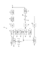
図10は、実施の形態6に係る歪み補償電力増幅器の概略構成を示すブロック図である。同図に示す実施の形態6に係る歪み補償電力増幅器6は、ADC18のビット数が十分確保できない場合にも歪み係数Akを精度良く求めることができるものである。前述した図8に示す実施の形態5に係る歪み補償電力増幅器5との違いは、相殺信号生成部22、DAC23、合成部24及び振幅調整部25を備えている点である。相殺信号生成部22は、テスト信号xtと同じ2波正弦波を相殺信号として生成するとともに、相殺信号の振幅、位相、遅延を調整する。DAC23は、相殺信号をアナログ信号に変換する。合成部24は、DAC23から出力される信号と、周波数変換部17から出力される信号とを合成する。振幅調整部25は、ADC18の入力レンジに合うように、合成部24から出力される信号の振幅を調整する。
(Embodiment 6)
FIG. 10 is a block diagram showing a schematic configuration of a distortion compensating power amplifier according to the sixth embodiment. Distortion compensating power amplifier 6 according to the sixth embodiment shown in the drawing, in which can be found in high accuracy distortion coefficients A k even when the number of bits of the ADC18 can not be sufficiently ensured. A difference from the distortion compensation power amplifier 5 according to the fifth embodiment shown in FIG. 8 described above is that a cancellation
図11は、実施の形態6に係る歪み補償電力増幅器6における歪み係数Akを求める処理を説明するためのフローチャートである。図11において前述した図9のフローチャートと同じ動作をするステップには、同じ番号を付与して説明を省略する。ステップS100からステップS200までは、相殺信号生成部22から何も出力しない状態で実行される。ステップS200で、フーリエ変換部12がフーリエ変換を実行し、ω1成分とω2成分のフーリエ係数であるZ1を取得する。次いで、ステップS210で、相殺信号生成部22が相殺信号を出力する。次いで、ステップS220で、相殺信号生成部22が、フーリエ変換部12の出力を観測しながら、フーリエ変換部12に入力される信号のうち相殺信号に含まれる周波数成分と同じ成分が小さくなるように、相殺信号の振幅、位相、遅延を調整する。次いで、ステップS230で、振幅調整部25が、ADC18に入力される信号のレベルがADCの入力レンジに近くなるようにゲインを調整する。次いで、ステップS240で、フーリエ変換部12が、フーリエ変換を実行し、フーリエ係数Z3、Z5、…を取得する。次いで、ステップS300で、補償係数演算部19が、ステップS200で取得されたZ1と、ステップS240で取得されたZ3、Z5、…と、振幅調整部25のゲインを元に歪み係数Akを求め、式(7)に基づいて歪み係数Akから補償係数Bkを求める。ここで、歪み係数Akを求める際には、フーリエ係数Z1を求める際の振幅調整部25のゲインと、フーリエ係数Z3、Z5、…を求める際の振幅調整部25のゲインが異なるので、そのゲイン差を補正する必要がある。ステップS200でフーリエ係数Z1を求める際の振幅調整部25のゲインに対する、ステップS240でフーリエ係数Z3、Z5、…を求める際の振幅調整部25のゲインをGとすると、歪み係数Akを求めるための式(11)は式(19)のように書きかえられる。式(19)を解くことでフーリエ係数を求める際の振幅調整部25のゲイン差を補正できるので、歪み係数Akを正しく求めることができる。
図12は、実施の形態6に係る歪み補償電力増幅器6における主要な信号を表わす図である。図12(a)は、テスト信号生成部10から出力されるテスト信号である。テスト信号として、ω1,ω2の周波数成分を持つ2波正弦波が出力される。図12(b)は、周波数変換部17から出力される信号である。例として、電力増幅器11での非線形歪みにより、2ω1−ω2、2ω2−ω1、3ω1−2ω2、3ω2−2ω1の周波数成分が発生している場合を示す。図12(c)は、相殺信号生成部22から出力される相殺信号である。図12(c)に示す相殺信号は、電力増幅器11から出力される信号の周波数成分のうち、ω1、ω2の周波数成分から構成される。電力増幅器11から出力される信号の周波数成分のうち、相殺信号と同じ周波数成分を抑圧できるように振幅、位相、遅延を調整されている。
FIG. 12 is a diagram illustrating main signals in distortion compensation power amplifier 6 according to the sixth embodiment. FIG. 12A shows a test signal output from the test
図12(d)は、合成部24から出力される信号である。図12(d)では、図12(b)の信号と図12(c)の信号が合成された結果、ω1、ω2の周波数成分が抑圧されている。図12(e)は、振幅調整部25から出力される信号である。図12(e)では、図12(d)の信号がADC18の入力レンジまで増幅されている。図12(e)において、ω1、ω2の周波数成分が抑圧されているので、2ω1−ω2、2ω2−ω1、3ω1−2ω2、3ω2−2ω1の周波数成分は歪み無く増幅され、ADCの量子化誤差の影響を受けずに歪み係数を求めることができる。
FIG. 12D shows a signal output from the combining
このように、実施の形態6に係る歪み補償電力増幅器6によれば、電力増幅器11から出力される信号から信号レベルの大きな周波数成分を抑圧した後、ADC18の入力レンジまで増幅してから歪み係数Akを求めるので、ADCのビット数が十分確保できない場合にも精度良く歪み係数Akを求めることができる。
As described above, according to the distortion compensating power amplifier 6 according to the sixth embodiment, after suppressing a frequency component having a large signal level from the signal output from the
なお、上述した実施の形態1〜6では、テスト信号として2波正弦波を用いる場合を例として説明したが、3波以上の正弦波を用いてもよい。 In the first to sixth embodiments described above, the case where two sine waves are used as the test signal has been described as an example, but three or more sine waves may be used.
また、上述した実施の形態1〜6では、フーリエ変換部12の動作として、フーリエ変換を行うものとして説明したが、FFT(Fast Fourier Transform:高速フーリエ変換)を行うものとしても構わない。または、複数のバンドパスフィルタとしても構わない。原理的に、特定の周波数成分を抽出することが可能であればよい。
In the first to sixth embodiments described above, the operation of the
また、上述した実施の形態3及び5において、タイミング調整部20における信号の振幅値を観測する期間をテスト信号の1周期としても構わないし、2周期以上としてもよい。2周期以上観測して複数回最大値を検出することでノイズ等の外乱の影響を軽減でき、精度良くフーリエ変換するタイミングを決定することができる。
In the third and fifth embodiments described above, the period for observing the amplitude value of the signal in the
また、上述した実施の形態3及び5では、タイミング調整部20を、フーリエ変換部12に入力される信号の振幅値が最大となるタイミングを検出するものとして説明したが、周期関数であるテスト信号の基準となるタイミングを検出できれば他の方法でも構わないし、振幅値が最小となるタイミングを検出するようにしてもよい。また、振幅値の絶対値が最大となるタイミング、振幅値の絶対値が最小となるタイミングを検出してもよい。さらに、ADC18から出力される信号がI、Qの複素信号である場合には、複素信号の絶対値、または、電力値が最大となるタイミングや最小となるタイミングを検出してもよい。
In the third and fifth embodiments described above, the
また、上述した実施の形態1〜6において、プリディストーション部14における式(2)の演算が、入力信号xに対して出力信号yとなるLUT(Look-up Table)として実現してもよい。
In Embodiments 1 to 6 described above, the calculation of Expression (2) in the
また、上述した実施の形態6では、相殺信号が2波正弦波である場合を例として説明したが、それ以上の数の正弦波を用いてもよい。ここで、図13を用いて、4波の正弦波を相殺信号として用いる場合を説明する。図13(a)、図13(b)は、それぞれ、図12(a)、図12(b)と同じである。図13(c)は、相殺信号生成部22から出力される相殺信号である。図13(c)に示す相殺信号は、電力増幅器11から出力される信号の周波数成分のうち、ω1、ω2、2ω1−ω2、2ω2−ω1の周波数成分から構成される。電力増幅器11から出力される信号の周波数成分のうち、相殺信号と同じ周波数成分を抑圧できるように振幅、位相、遅延を調整されている。
Further, in the above-described sixth embodiment, the case where the cancellation signal is a two-wave sine wave has been described as an example, but a larger number of sine waves may be used. Here, the case where four sine waves are used as the cancellation signal will be described with reference to FIG. 13 (a) and 13 (b) are the same as FIGS. 12 (a) and 12 (b), respectively. FIG. 13C shows a cancellation signal output from the cancellation
図13(d)は、合成部24から出力される信号である。図13(d)では、図13(b)の信号と図13(c)の信号が合成された結果、ω1、ω2、2ω1−ω2、2ω2−ω1の周波数成分が抑圧されている。図13(e)は、振幅調整部25から出力される信号である。図13(e)では、図13(d)の信号がADC18の入力レンジまで増幅されている。図13(e)において、ω1、ω2、2ω1−ω2、2ω2−ω1の周波数成分が抑圧されているので、3ω1−2ω2、3ω2−2ω1の周波数成分は歪み無く増幅され、ADC18の量子化誤差の影響を受けずに歪み係数を求めることができる。
FIG. 13D shows a signal output from the
(実施の形態6の変形例)
図14は、実施の形態6に係る歪み補償電力増幅器6の変形例における歪み係数Akを求める処理を説明するためのフローチャートである。実施の形態6に係る歪み補償電力増幅器6の変形例では、図12(c)に示す2波の相殺信号と、図13(c)に示す4波の相殺信号を用いる。図14において前述した図11のフローチャートと同じ動作をするステップには、同じ番号を付与して説明を省略する。ステップS100からステップS230までは、図11のフローチャートと同じである。但し、ステップS200で取得されるフーリエ係数Z1は、第1のフーリエ係数に対応する。ステップS230で、振幅調整部25が図12(e)に示す信号を出力する。次いで、ステップS250で、フーリエ変換部12がフーリエ変換を行い、2ω1−ω2、2ω2−ω1の成分のフーリエ係数であるZ3(第2のフーリエ係数に対応)を求める。次いで、ステップS260で、相殺信号生成部22が図13(c)に示す4波の相殺信号を出力する。次いで、ステップS270で、相殺信号生成部22がフーリエ変換部12の出力を観測しながら、フーリエ変換部12に入力される信号のうち相殺信号に含まれる周波数成分と同じ成分が小さくなるように、相殺信号の振幅、位相、遅延を調整する。
(Modification of Embodiment 6)
FIG. 14 is a flowchart for explaining processing for obtaining the distortion coefficient Ak in the modification of the distortion compensating power amplifier 6 according to the sixth embodiment. In the modification of the distortion compensating power amplifier 6 according to the sixth embodiment, a two-wave cancellation signal shown in FIG. 12C and a four-wave cancellation signal shown in FIG. 13C are used. In FIG. 14, steps that perform the same operations as those in the flowchart of FIG. Steps S100 to S230 are the same as those in the flowchart of FIG. However, the Fourier coefficients Z 1 acquired in step S200 corresponds to the first Fourier coefficient. In step S230, the
次いで、ステップS280で、振幅調整部25が、ADC18に入力される信号のレベルがADCの入力レンジに近くなるようにゲインを調整する。この時、振幅調整部25から出力される信号は図13(e)のようになっている。次いで、ステップS290で、フーリエ変換部12がフーリエ変換を実行し、フーリエ係数Z5、Z7、…(第3のフーリエ係数以降)を取得する。次いで、ステップS300で、歪み係数演算部13が、ステップS200で取得されたZ1と、ステップS250で取得されたZ3と、ステップS290で取得されたZ5、Z7、…と、振幅調整部25のゲインを元に歪み係数Akを求める。そして、補償係数演算部19が、式(7)に基づいて歪み係数Akから補償係数Bkを求める。ここで、ステップS200でフーリエ係数Z1を求める際の振幅調整部25のゲインに対する、ステップS250でフーリエ係数Z3を求める際の振幅調整部25のゲインをG2とする。また、ステップS200でフーリエ係数Z1を求める際の振幅調整部25のゲインに対する、ステップS290でフーリエ係数Z5、Z7、…を求める際の振幅調整部25のゲインをG3とする。G2、G3を用いて、歪み係数Akを求めるための式(11)は式(20)のように書きかえられる。式(20)を解くことでフーリエ係数を求める際の振幅調整部25のゲイン差を補正できるので、歪み係数Akを正しく求めることができる。
図11のフローチャートでは、まずフーリエ係数Z1を求めた後、相殺信号を出力してフーリエ係数Z3、Z5、…を求めていたのに対し、図14のフローチャートでは、まずフーリエ係数Z1を求めた後、2波の相殺信号を出力してフーリエ係数Z3を求め、さらにその後、4波の相殺信号を出力してフーリエ係数Z5、Z7、…を求めている。このように段階的にフーリエ係数を求めることで、ADC18の量子化誤差の影響を軽減し、歪み係数Akを精度良く求めることができる。
In the flowchart of FIG. 11, after firstly calculated Fourier coefficients Z 1, Fourier coefficients Z 3, Z 5 and outputs the cancellation signal, whereas had sought ..., in the flowchart of FIG. 14, the Fourier coefficients Z 1 , The two-wave cancellation signal is output to determine the Fourier coefficient Z 3 , and then the four-wave cancellation signal is output to determine the Fourier coefficients Z 5 , Z 7 ,. By obtaining the Fourier coefficient step by step in this way, the influence of the quantization error of the
(本開示の一態様の概要)
本開示の第1の非線形歪み検出装置は、電力増幅器で発生する非線形歪みを検出する非線形歪み検出装置であって、テスト信号を生成し前記電力増幅器に出力するテスト信号生成部と、前記電力増幅器の出力信号を周波数領域の信号に変換するフーリエ変換部と、前記フーリエ変換部から得られる振幅情報および位相情報に基づいて前記電力増幅器の歪み係数を演算する歪み係数演算部と、を備える。
(Overview of one aspect of the present disclosure)
A first nonlinear distortion detection device of the present disclosure is a nonlinear distortion detection device that detects nonlinear distortion generated in a power amplifier, and generates a test signal and outputs the test signal to the power amplifier, and the power amplifier A Fourier transform unit that converts the output signal into a frequency domain signal, and a distortion coefficient computation unit that computes a distortion coefficient of the power amplifier based on amplitude information and phase information obtained from the Fourier transform unit.
また、本開示の第2の非線形歪み検出装置は、第1の非線形歪み検出装置であって、前記テスト信号は2波正弦波である。 The second nonlinear distortion detection apparatus of the present disclosure is the first nonlinear distortion detection apparatus, and the test signal is a two-wave sine wave.
また、本開示の第3の非線形歪み検出装置は、第1又は第2の非線形歪み検出装置であって、さらに、前記フーリエ変換部が周波数領域の信号に変換するためのタイミングを調整するタイミング調整部を備え、前記タイミング調整部は、前記フーリエ変換部に入力される信号の振幅値を元に周波数領域の信号に変換するためのタイミングを調整する。 Further, the third nonlinear distortion detection device of the present disclosure is the first or second nonlinear distortion detection device, and further, timing adjustment for adjusting timing for the Fourier transform unit to convert the signal into a frequency domain signal. The timing adjustment unit adjusts the timing for conversion to a frequency domain signal based on the amplitude value of the signal input to the Fourier transform unit.
また、本開示の第4の非線形歪み検出装置は、第1ないし第3のいずれか1つの非線形歪み検出装置であって、さらに、前記テスト信号の位相を調整する位相調整部を備え、前記位相調整部は、前記フーリエ変換部から得られる位相情報を元に前記テスト信号に位相回転を与える。 The fourth nonlinear distortion detection device of the present disclosure is any one of the first to third nonlinear distortion detection devices, further including a phase adjustment unit that adjusts the phase of the test signal, and the phase The adjustment unit gives a phase rotation to the test signal based on the phase information obtained from the Fourier transform unit.
また、本開示の第5の非線形歪み検出装置は、第1ないし第4のいずれか1つの非線形歪み検出装置であって、さらに、相殺信号を生成し、前記相殺信号の振幅、位相、遅延を調整する相殺信号生成部と、前記相殺信号と前記電力増幅器の出力信号を合成する合成部と、前記合成部の出力信号の振幅を調整する振幅調整部と、前記振幅調整部の出力信号をデジタル信号に変換するADCと、を備え、前記フーリエ変換部は前記ADCの出力信号を周波数領域の信号に変換し、前記歪み係数演算部は、前記電力増幅器の出力信号に前記相殺信号を合成しない状態で前記フーリエ変換部から得られる振幅情報および位相情報を第1の振幅位相情報として取得し、前記電力増幅器の出力信号に前記相殺信号を合成した状態で前記フーリエ変換部から得られる振幅情報および位相情報を第2の振幅位相情報として取得し、前記第1の振幅位相情報と前記第2の振幅位相情報とに基づいて歪み係数を演算する。 The fifth nonlinear distortion detection device of the present disclosure is any one of the first to fourth nonlinear distortion detection devices, further generates a cancellation signal, and calculates the amplitude, phase, and delay of the cancellation signal. An offset signal generation unit to adjust, a synthesis unit that synthesizes the cancellation signal and the output signal of the power amplifier, an amplitude adjustment unit that adjusts the amplitude of the output signal of the synthesis unit, and an output signal of the amplitude adjustment unit that is digital An ADC that converts the signal into a signal, the Fourier transform unit converts the output signal of the ADC into a frequency domain signal, and the distortion coefficient calculation unit does not synthesize the cancellation signal with the output signal of the power amplifier. And obtaining the amplitude information and phase information obtained from the Fourier transform unit as first amplitude phase information, and combining the cancellation signal with the output signal of the power amplifier from the Fourier transform unit. It is to get the amplitude information and phase information as a second amplitude phase information, and calculates the distortion coefficient based on the said first amplitude and phase information the second amplitude phase information.
また、本開示の第6の非線形歪み検出装置は、第5の非線形歪み検出装置であって、前記相殺信号は2波正弦波である。 The sixth nonlinear distortion detection apparatus of the present disclosure is a fifth nonlinear distortion detection apparatus, and the cancellation signal is a two-wave sine wave.
また、本開示の第7の非線形歪み検出装置は、第5の非線形歪み検出装置であって、前記相殺信号は4波正弦波である。 The seventh nonlinear distortion detection device of the present disclosure is a fifth nonlinear distortion detection device, and the cancellation signal is a four-wave sine wave.
また、本開示の第8の非線形歪み検出装置は、第5の非線形歪み検出装置であって、前記相殺信号は2波正弦波および4波正弦波であり、前記フーリエ変換部は、第1のフーリエ係数を求めた後、前記相殺信号生成部から2波正弦波の相殺信号が出力され第2のフーリエ係数を求め、さらにその後、前記相殺信号生成部から4波正弦波の相殺信号が出力され第3のフーリエ係数以降を求める。 The eighth nonlinear distortion detection device of the present disclosure is a fifth nonlinear distortion detection device, wherein the canceling signal is a two-wave sine wave and a four-wave sine wave, and the Fourier transform unit is After obtaining the Fourier coefficient, a cancellation signal with a two-wave sine wave is output from the cancellation signal generation unit to obtain a second Fourier coefficient, and then a cancellation signal with a four-wave sine wave is output from the cancellation signal generation unit. After the third Fourier coefficient is obtained.
また、本開示の歪み補償電力増幅器は、電力増幅器のプリディストーションを行う歪み補償電力増幅器であって、テスト信号を生成し出力するテスト信号生成部と、前記テスト信号を入力とする電力増幅器と、前記電力増幅器の出力信号を周波数領域の信号に変換するフーリエ変換部と、前記フーリエ変換部から得られる振幅情報および位相情報に基づいて前記電力増幅器の歪み係数を演算する歪み係数演算部と、前記歪み係数からプリディストーションを行うための補償係数を演算する補償係数演算部と、前記補償係数を用いてプリディストーションを行うプリディストーション部と、を備え、前記歪み係数を演算する時は前記テスト信号が前記電力増幅器に入力され、入力信号を送信する時は前記補償係数を用いてプリディストーションした信号が前記電力増幅器に入力される。 Further, the distortion compensation power amplifier of the present disclosure is a distortion compensation power amplifier that performs predistortion of the power amplifier, a test signal generation unit that generates and outputs a test signal, a power amplifier that receives the test signal, and A Fourier transform unit that converts an output signal of the power amplifier into a signal in a frequency domain; a distortion coefficient computation unit that computes a distortion coefficient of the power amplifier based on amplitude information and phase information obtained from the Fourier transform unit; A compensation coefficient calculation unit that calculates a compensation coefficient for performing predistortion from a distortion coefficient, and a predistortion unit that performs predistortion using the compensation coefficient, and when the distortion coefficient is calculated, the test signal is Predistortion using the compensation coefficient when transmitting the input signal input to the power amplifier Signal is input to the power amplifier.
以上、図面を参照しながら各種の実施の形態について説明したが、本開示はかかる例に限定されないことは言うまでもない。当業者であれば、特許請求の範囲に記載された範疇内において、各種の変更例または修正例に想到し得ることは明らかであり、それらについても当然に本発明の技術的範囲に属するものと了解される。 While various embodiments have been described above with reference to the drawings, it goes without saying that the present disclosure is not limited to such examples. It will be apparent to those skilled in the art that various changes and modifications can be made within the scope of the claims, and these are naturally within the technical scope of the present invention. Understood.
本開示は、無線LANやZigBee(登録商標)、Bluetooth(登録商標)等の各種無線通信装置に適用できる。特に、FFT回路を持つ無線通信装置、例えば、変復調方式にOFDM(Orthogonal Frequency Division Multiplex)方式を用いる無線通信装置や、等化器にFDE(Frequency Domain Equalizer)方式を用いる無線通信装置などに有用である。 The present disclosure can be applied to various wireless communication devices such as a wireless LAN, ZigBee (registered trademark), and Bluetooth (registered trademark). In particular, it is useful for a wireless communication device having an FFT circuit, for example, a wireless communication device using an OFDM (Orthogonal Frequency Division Multiplex) method as a modulation / demodulation method, or a wireless communication device using an FDE (Frequency Domain Equalizer) method as an equalizer. is there.
1 非線形歪み検出装置
2〜6 歪み補償電力増幅器
10 テスト信号生成部
11 電力増幅器
12 フーリエ変換部
13 歪み係数演算部
14 プリディストーション部
15、23 DAC
16、17 周波数変換部
18 ADC
19 補償係数演算部
20 タイミング調整部
21 位相調整部
22 相殺信号生成部
24 合成部
25 振幅調整部
DESCRIPTION OF SYMBOLS 1 Nonlinear distortion detection apparatus 2-6 Distortion
16, 17
DESCRIPTION OF
Claims (8)
テスト信号を生成し前記電力増幅器に出力するテスト信号生成部と、
前記電力増幅器の出力信号を周波数領域の信号に変換するフーリエ変換部と、
前記フーリエ変換部から得られる振幅情報および位相情報に基づいて前記電力増幅器の歪み係数を演算する歪み係数演算部と、
相殺信号を生成し、前記相殺信号の振幅、位相、遅延を調整する相殺信号生成部と、
前記相殺信号と前記電力増幅器の出力信号を合成する合成部と、
前記合成部の出力信号の振幅を調整する振幅調整部と、
前記振幅調整部の出力信号をデジタル信号に変換するADCと、を備え、
前記フーリエ変換部は前記ADCの出力信号を周波数領域の信号に変換し、
前記歪み係数演算部は、前記電力増幅器の出力信号に前記相殺信号を合成しない状態で前記フーリエ変換部から得られる振幅情報および位相情報を第1の振幅位相情報として取得し、前記電力増幅器の出力信号に前記相殺信号を合成した状態で前記フーリエ変換部から得られる振幅情報および位相情報を第2の振幅位相情報として取得し、前記第1の振幅位相情報と前記第2の振幅位相情報とに基づいて歪み係数を演算することを特徴とする非線形歪み検出装置。 A non-linear distortion detecting device for detecting non-linear distortion generated in a power amplifier,
A test signal generator that generates a test signal and outputs the test signal to the power amplifier;
A Fourier transform unit for converting the output signal of the power amplifier into a signal in the frequency domain;
A distortion coefficient calculation unit that calculates a distortion coefficient of the power amplifier based on amplitude information and phase information obtained from the Fourier transform unit;
A cancellation signal generating unit that generates a cancellation signal and adjusts the amplitude, phase, and delay of the cancellation signal;
A combining unit that combines the cancellation signal and the output signal of the power amplifier;
An amplitude adjusting unit for adjusting the amplitude of the output signal of the combining unit;
An ADC that converts the output signal of the amplitude adjustment unit into a digital signal,
The Fourier transform unit converts the output signal of the ADC into a frequency domain signal,
The distortion coefficient calculation unit obtains amplitude information and phase information obtained from the Fourier transform unit without combining the cancellation signal with the output signal of the power amplifier as first amplitude phase information, and outputs the power amplifier Amplitude information and phase information obtained from the Fourier transform unit in a state in which the cancellation signal is combined with a signal is acquired as second amplitude phase information, and the first amplitude phase information and the second amplitude phase information are obtained. A non-linear distortion detecting apparatus, wherein a distortion coefficient is calculated based on the distortion coefficient .
前記タイミング調整部は、前記フーリエ変換部に入力される信号の振幅値を元に周波数領域の信号に変換するためのタイミングを調整することを特徴とする請求項1または請求項2に記載の非線形歪み検出装置。 Furthermore, a timing adjustment unit that adjusts timing for the Fourier transform unit to convert the signal into a frequency domain signal,
3. The non-linearity according to claim 1, wherein the timing adjustment unit adjusts a timing for conversion to a frequency domain signal based on an amplitude value of a signal input to the Fourier transform unit. 4. Strain detector.
前記位相調整部は、前記フーリエ変換部から得られる位相情報を元に前記テスト信号に位相回転を与えることを特徴とする請求項1から請求項3のいずれか一項に記載の非線形歪み検出装置。 Furthermore, a phase adjustment unit for adjusting the phase of the test signal is provided,
4. The nonlinear distortion detection apparatus according to claim 1, wherein the phase adjustment unit applies phase rotation to the test signal based on phase information obtained from the Fourier transform unit. 5. .
前記フーリエ変換部は、第1のフーリエ係数を求めた後、前記相殺信号生成部から2波正弦波の相殺信号が出力され第2のフーリエ係数を求め、さらにその後、前記相殺信号生成部から4波正弦波の相殺信号が出力され第3のフーリエ係数以降を求めることを特徴とする請求項1に記載の非線形歪み検出装置。 The cancellation signal is a two-wave sine wave and a four-wave sine wave,
The Fourier transform unit obtains a first Fourier coefficient, obtains a second Fourier coefficient by outputting a two-wave sine wave cancellation signal from the cancellation signal generation unit, and then obtains a second Fourier coefficient from the cancellation signal generation unit. The nonlinear distortion detection device according to claim 1 , wherein a cancellation signal of a wave sine wave is output to obtain the third Fourier coefficient and the subsequent ones.
テスト信号を生成し出力するテスト信号生成部と、
前記テスト信号を入力とする電力増幅器と、
前記電力増幅器の出力信号を周波数領域の信号に変換するフーリエ変換部と、
前記フーリエ変換部から得られる振幅情報および位相情報に基づいて前記電力増幅器の歪み係数を演算する歪み係数演算部と、
前記歪み係数からプリディストーションを行うための補償係数を演算する補償係数演算部と、
前記補償係数を用いてプリディストーションを行うプリディストーション部と、を備え、
前記歪み係数を演算する時は前記テスト信号が前記電力増幅器に入力され、
入力信号を送信する時は前記補償係数を用いてプリディストーションした信号が前記電力増幅器に入力され、
さらに、相殺信号を生成し、前記相殺信号の振幅、位相、遅延を調整する相殺信号生成部と、
前記相殺信号と前記電力増幅器の出力信号を合成する合成部と、
前記合成部の出力信号の振幅を調整する振幅調整部と、
前記振幅調整部の出力信号をデジタル信号に変換するADCと、を備え、
前記フーリエ変換部は前記ADCの出力信号を周波数領域の信号に変換し、
前記歪み係数演算部は、前記電力増幅器の出力信号に前記相殺信号を合成しない状態で前記フーリエ変換部から得られる振幅情報および位相情報を第1の振幅位相情報として取得し、前記電力増幅器の出力信号に前記相殺信号を合成した状態で前記フーリエ変換部から得られる振幅情報および位相情報を第2の振幅位相情報として取得し、前記第1の振幅位相情報と前記第2の振幅位相情報とに基づいて歪み係数を演算することを特徴とする歪み補償電力増幅器。 A distortion compensated power amplifier for predistorting the power amplifier,
A test signal generator for generating and outputting a test signal;
A power amplifier receiving the test signal;
A Fourier transform unit for converting the output signal of the power amplifier into a signal in the frequency domain;
A distortion coefficient calculation unit that calculates a distortion coefficient of the power amplifier based on amplitude information and phase information obtained from the Fourier transform unit;
A compensation coefficient calculator for calculating a compensation coefficient for predistortion from the distortion coefficient;
A predistortion unit that performs predistortion using the compensation coefficient,
When calculating the distortion coefficient, the test signal is input to the power amplifier,
When transmitting the input signal, the predistorted signal using the compensation coefficient is input to the power amplifier ,
Further, a cancellation signal is generated, and a cancellation signal generator for adjusting the amplitude, phase, and delay of the cancellation signal;
A combining unit that combines the cancellation signal and the output signal of the power amplifier;
An amplitude adjusting unit for adjusting the amplitude of the output signal of the combining unit;
An ADC that converts the output signal of the amplitude adjustment unit into a digital signal,
The Fourier transform unit converts the output signal of the ADC into a frequency domain signal,
The distortion coefficient calculation unit obtains amplitude information and phase information obtained from the Fourier transform unit without combining the cancellation signal with the output signal of the power amplifier as first amplitude phase information, and outputs the power amplifier Amplitude information and phase information obtained from the Fourier transform unit in a state in which the cancellation signal is combined with a signal is acquired as second amplitude phase information, and the first amplitude phase information and the second amplitude phase information are obtained. A distortion compensation power amplifier characterized by calculating a distortion coefficient based on the distortion coefficient .
Priority Applications (2)
| Application Number | Priority Date | Filing Date | Title |
|---|---|---|---|
| JP2014033041A JP6340207B2 (en) | 2014-02-24 | 2014-02-24 | Nonlinear distortion detector and distortion compensation power amplifier |
| US14/623,239 US9903908B2 (en) | 2014-02-24 | 2015-02-16 | Nonlinear distortion detection device and distortion compensation power amplifier |
Applications Claiming Priority (1)
| Application Number | Priority Date | Filing Date | Title |
|---|---|---|---|
| JP2014033041A JP6340207B2 (en) | 2014-02-24 | 2014-02-24 | Nonlinear distortion detector and distortion compensation power amplifier |
Publications (2)
| Publication Number | Publication Date |
|---|---|
| JP2015159420A JP2015159420A (en) | 2015-09-03 |
| JP6340207B2 true JP6340207B2 (en) | 2018-06-06 |
Family
ID=53881979
Family Applications (1)
| Application Number | Title | Priority Date | Filing Date |
|---|---|---|---|
| JP2014033041A Expired - Fee Related JP6340207B2 (en) | 2014-02-24 | 2014-02-24 | Nonlinear distortion detector and distortion compensation power amplifier |
Country Status (2)
| Country | Link |
|---|---|
| US (1) | US9903908B2 (en) |
| JP (1) | JP6340207B2 (en) |
Families Citing this family (5)
| Publication number | Priority date | Publication date | Assignee | Title |
|---|---|---|---|---|
| US10057020B2 (en) * | 2015-11-19 | 2018-08-21 | Tektronix, Inc. | Joint estimation of coefficients for skew, gain imbalance and channel response for signal sources |
| EP3470862B1 (en) | 2017-10-10 | 2022-03-02 | Melexis Bulgaria Ltd. | Sensor defect diagnostic circuit |
| CN109507517B (en) * | 2018-12-07 | 2020-10-27 | 国网辽宁省电力有限公司鞍山供电公司 | Distribution transformer operation state analysis method based on double-side power big data comparison |
| EP4024892A4 (en) * | 2019-08-27 | 2022-10-12 | Panasonic Intellectual Property Management Co., Ltd. | Signal processing device and adjustment method |
| US11467151B1 (en) * | 2021-12-23 | 2022-10-11 | United Arab Emirates University | Phosphorescence oxygen analyzer and uses thereof |
Family Cites Families (9)
| Publication number | Priority date | Publication date | Assignee | Title |
|---|---|---|---|---|
| US4672565A (en) * | 1981-03-10 | 1987-06-09 | Nippon Soken, Inc. | Direction detecting system for vehicles |
| JPH05121958A (en) * | 1991-10-29 | 1993-05-18 | Saitama Nippon Denki Kk | Distortion compensation control system for linear amplifier |
| JP3166321B2 (en) * | 1992-07-01 | 2001-05-14 | 日本電気株式会社 | Modulated signal transmission system |
| EP0707767B1 (en) * | 1993-07-09 | 1997-05-14 | Edmunde Eugene Newhall | Systems with increased information rates using embedded sample modulation and predistortion equalization |
| JP2005079935A (en) | 2003-09-01 | 2005-03-24 | Rikogaku Shinkokai | Adaptive predistortion type distortion compensation power amplifier |
| JP4619402B2 (en) | 2005-02-01 | 2011-01-26 | 株式会社日立国際電気 | Spectral analysis method, distortion detection apparatus, distortion compensation amplification apparatus |
| JP2010154459A (en) | 2008-12-26 | 2010-07-08 | Hitachi Kokusai Electric Inc | High-frequency amplifying device |
| JP5113871B2 (en) * | 2009-05-21 | 2013-01-09 | 株式会社エヌ・ティ・ティ・ドコモ | Power series digital predistorter and control method thereof |
| JP5682382B2 (en) * | 2011-03-09 | 2015-03-11 | 富士通セミコンダクター株式会社 | Receiving device, transmitting device, and correction method related to discrete sample timing thereof |
-
2014
- 2014-02-24 JP JP2014033041A patent/JP6340207B2/en not_active Expired - Fee Related
-
2015
- 2015-02-16 US US14/623,239 patent/US9903908B2/en not_active Expired - Fee Related
Also Published As
| Publication number | Publication date |
|---|---|
| JP2015159420A (en) | 2015-09-03 |
| US20150241494A1 (en) | 2015-08-27 |
| US9903908B2 (en) | 2018-02-27 |
Similar Documents
| Publication | Publication Date | Title |
|---|---|---|
| JP3875707B2 (en) | Distortion compensation device | |
| KR101077349B1 (en) | Linearization of rf power amplifiers using an adaptive subband predistorter | |
| JP4555702B2 (en) | Distortion compensation device | |
| JP6340207B2 (en) | Nonlinear distortion detector and distortion compensation power amplifier | |
| US20100074367A1 (en) | Adaptive combiner error calibration algorithms in all-digital outphasing transmitter | |
| US8442157B2 (en) | Wireless apparatus and signal processing method | |
| US8588711B2 (en) | Transmission apparatus and distortion compensation method | |
| JP4619827B2 (en) | Distortion compensation device | |
| JPWO2009090825A1 (en) | Predistorter | |
| JP4951074B2 (en) | Power series digital predistorter and its distortion compensation control method | |
| JP2007221245A (en) | Distortion compensation device and method | |
| CN107251420B (en) | Method, apparatus and non-transitory computer readable medium for vector signal alignment | |
| EP1345319A2 (en) | Method and system for reducing non-linearities | |
| US20170126261A1 (en) | Analog rf pre-distorter and non-linear splitter | |
| JP2014103540A (en) | Distortion compensation device, transmission device, distortion compensation method and transfer function calculation method | |
| JP2010258597A (en) | Apparatus for distortion compensation of power amplifier, and method of detecting failure in the same | |
| US8712345B2 (en) | Distortion compensation device, distortion compensation method, and radio transmitter | |
| CN107005527B (en) | Signal transmission device and signal transmission method | |
| US9225577B2 (en) | Exciter and quadrature error correction method | |
| JPWO2011086752A1 (en) | Amplifying device and signal processing device | |
| JP2017046122A (en) | Distortion compensation device | |
| JP5673238B2 (en) | Power amplification device, transmitter, and power amplification device control method | |
| JP5509455B2 (en) | Distortion compensation device | |
| US7816984B2 (en) | Lookup table generation method and related device for a predistorter | |
| JP2007288492A (en) | Distortion compensating device and distortion compensation method |
Legal Events
| Date | Code | Title | Description |
|---|---|---|---|
| A621 | Written request for application examination |
Free format text: JAPANESE INTERMEDIATE CODE: A621 Effective date: 20160829 |
|
| A977 | Report on retrieval |
Free format text: JAPANESE INTERMEDIATE CODE: A971007 Effective date: 20170830 |
|
| A131 | Notification of reasons for refusal |
Free format text: JAPANESE INTERMEDIATE CODE: A131 Effective date: 20170905 |
|
| A521 | Written amendment |
Free format text: JAPANESE INTERMEDIATE CODE: A523 Effective date: 20171006 |
|
| TRDD | Decision of grant or rejection written | ||
| A01 | Written decision to grant a patent or to grant a registration (utility model) |
Free format text: JAPANESE INTERMEDIATE CODE: A01 Effective date: 20180417 |
|
| A61 | First payment of annual fees (during grant procedure) |
Free format text: JAPANESE INTERMEDIATE CODE: A61 Effective date: 20180514 |
|
| R151 | Written notification of patent or utility model registration |
Ref document number: 6340207 Country of ref document: JP Free format text: JAPANESE INTERMEDIATE CODE: R151 |
|
| LAPS | Cancellation because of no payment of annual fees |